Embed Size (px)
Citation preview
Confidential
Market Watch Panel 5: PIC vs. Si Photonics: Hype or Reality?
1
Review Light Sources for PIC and Si-Photonics
Norman Kwong BinOptics Corporation
2014-3-13

Confidential
Motivation of PIC and Si Photonics Technologies
2
• Lower Cost
• Lower Power Consumption
• Smaller size, high density
• Device uniformity, higher yield
• Automated manufacturing
• Higher reliability and Long service life
Confidential
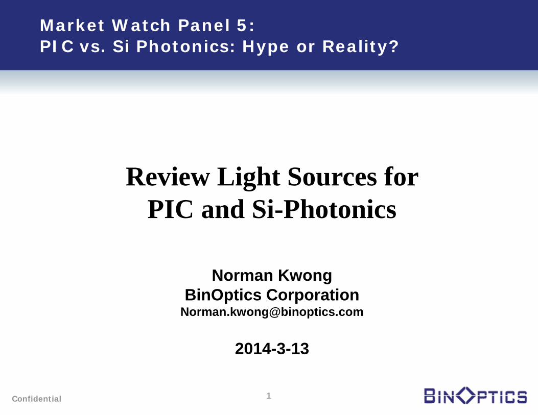
Comparing InP PIC and Silicon Photonics
3
InP base PIC Silicon Photonics
Light source Good light source material Need InP light source
Process complexity and maturity Less mature Very mature
Scale, wafer size Smaller size Large scale
Confidential
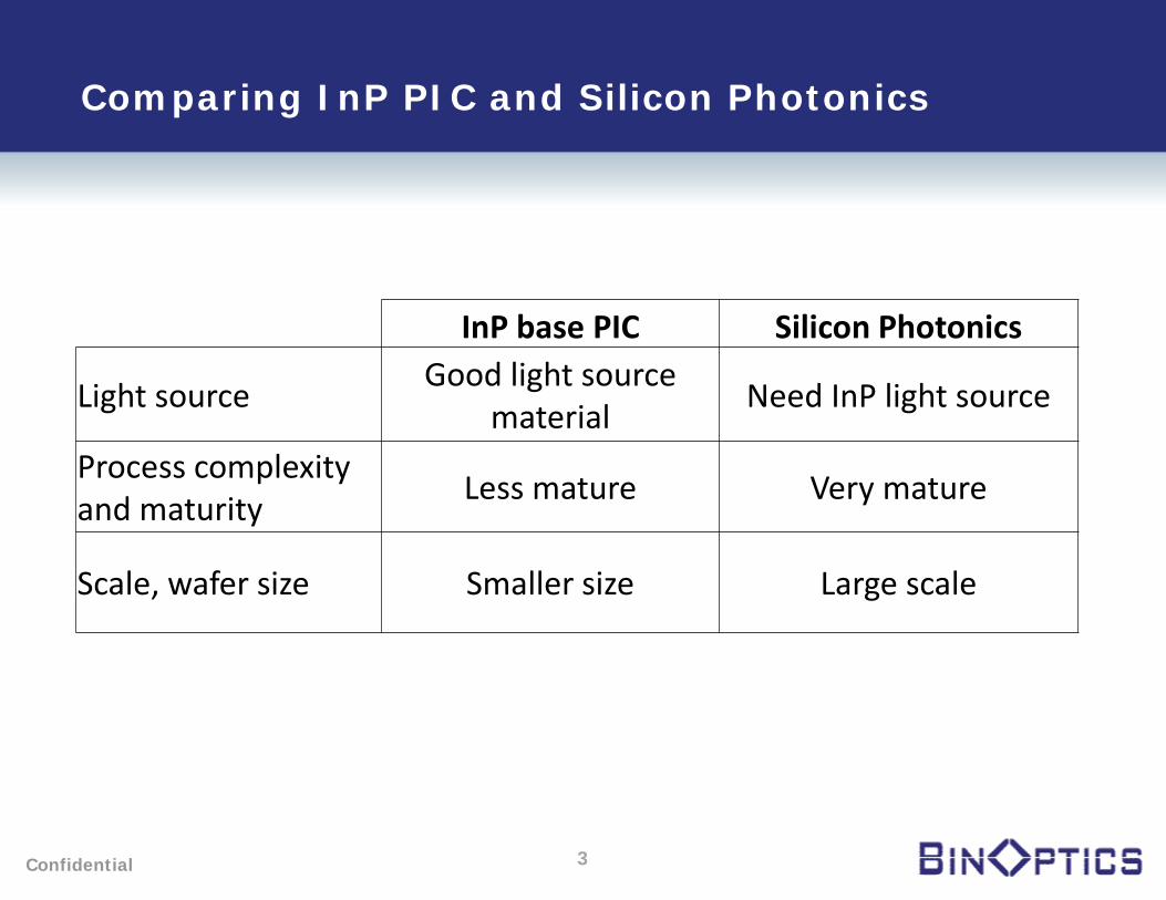
Summary of level of Integration in InP and Hybrid Silicon
4 Source: Martijn J. R. Heck (UCSB)
Confidential
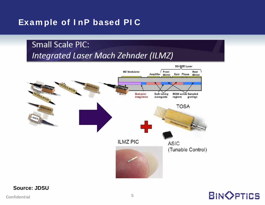
Example of InP based PIC
5
Source: JDSU
Confidential 6
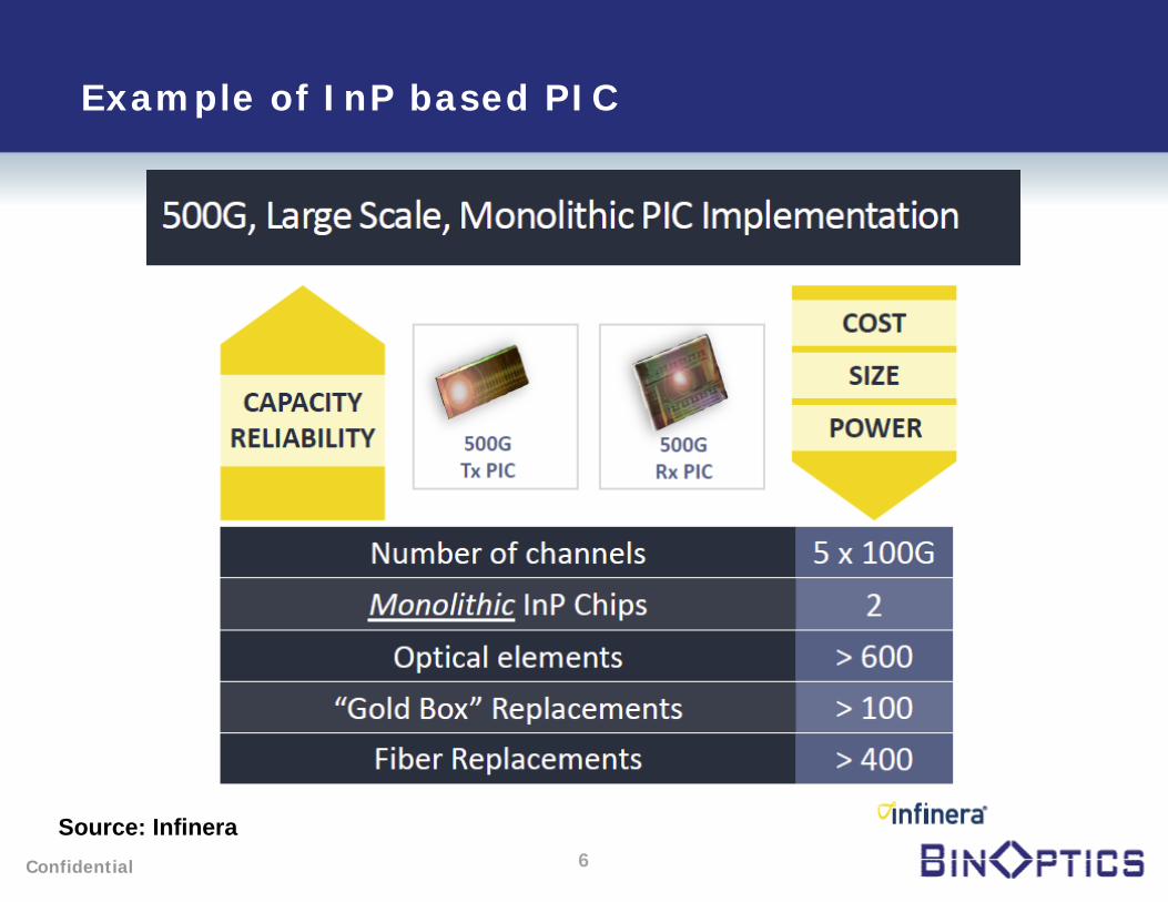
Example of InP based PIC
Source: Infinera
Confidential 7
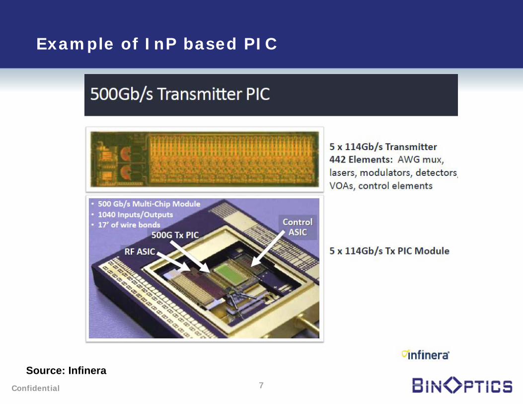
Example of InP based PIC
Source: Infinera
Confidential 8
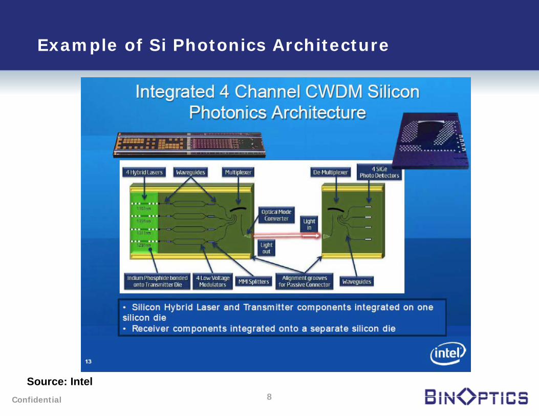
Source: Intel
Example of Si Photonics Architecture
Confidential
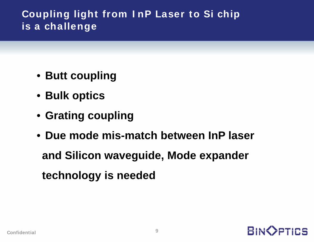
Coupling light from InP Laser to Si chip is a challenge
9
• Butt coupling
• Bulk optics
• Grating coupling
• Due mode mis-match between InP laser
and Silicon waveguide, Mode expander
technology is needed
Confidential 10
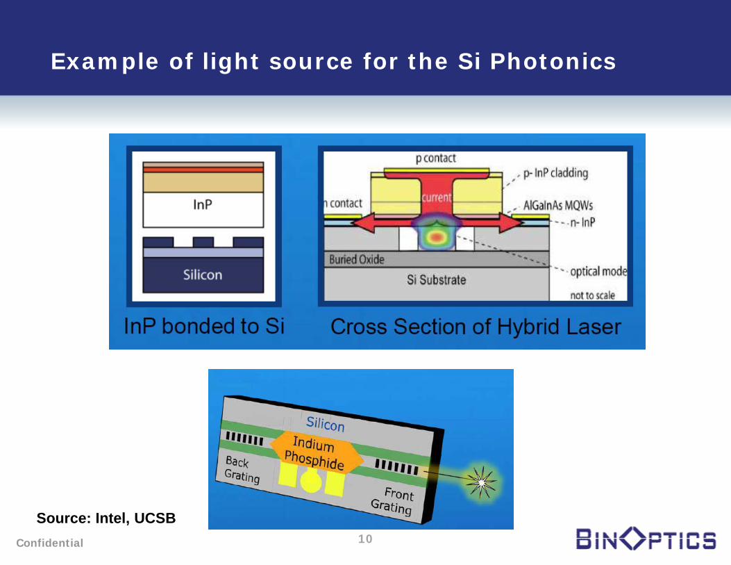
Example of light source for the Si Photonics
Source: Intel, UCSB

Confidential 11
Source: Luxtera
Example of light source for the Si Photonics

Confidential 12
New Device Technologies that enabling the PIC
and Si Photonics Devices
New Technologies

Confidential 13
Conventional Cleaved Facet Process Etched Facet Technology Process
Conventional vs. Etched Facet Technology
Waveguide Formation Contacts
Cleave to Form Mirrors
Stack & Coat Mirrors
Test
Package
Singulate
Singulate
Package
Test
Waveguide Formation
Contacts Etch Mirrors
Wafer Level Coatings
1
2
3
4
5
6
1
2
3
4
Over 50 million of laser sold using the EFT technology

Confidential 14
EFT provides extremely precise control of dimensions and allows designers to put two laser cavities on one chip
Designed so that one of two cavities operates with the correct phase
Up to a doubling of chip yield for DFB lasers
Dual Laser Cavity
Confidential
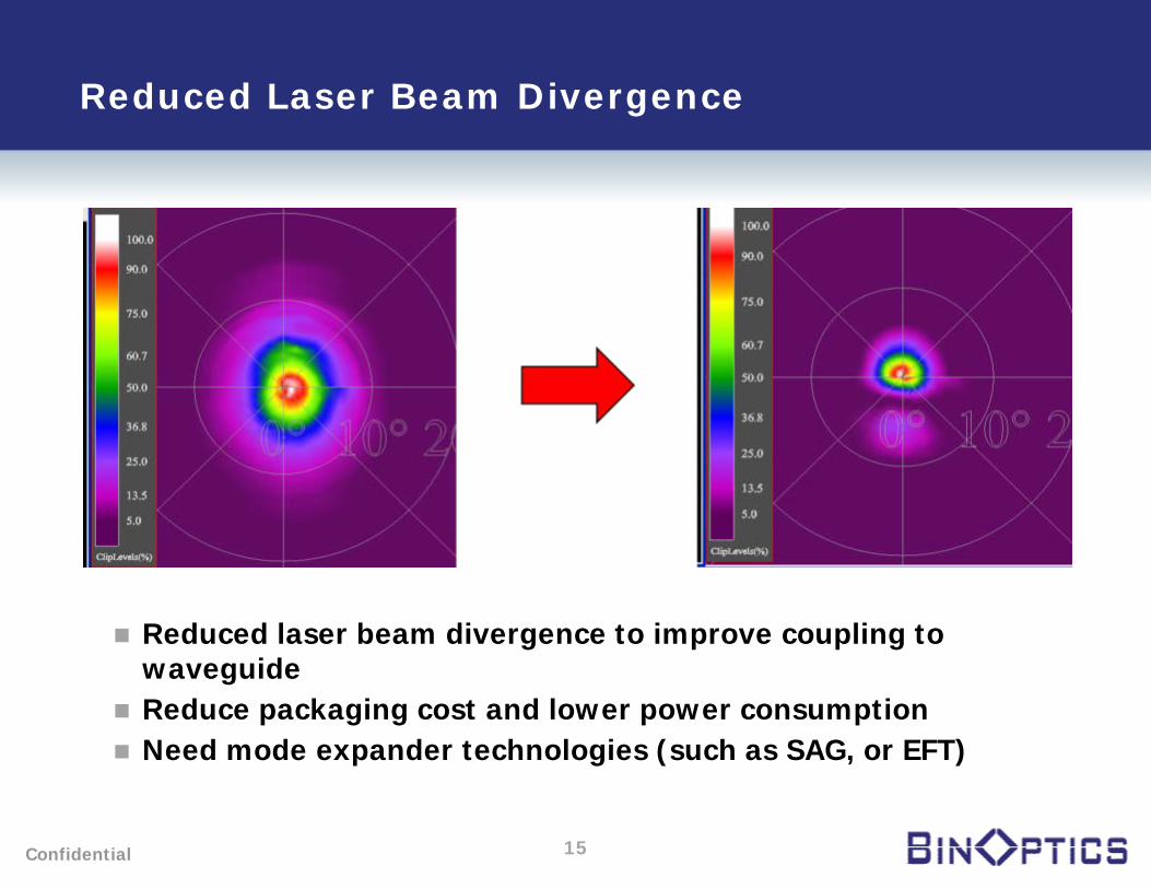
Reduced Laser Beam Divergence
15
Reduced laser beam divergence to improve coupling to waveguide
Reduce packaging cost and lower power consumption Need mode expander technologies (such as SAG, or EFT)
Confidential 16
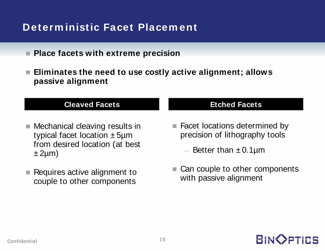
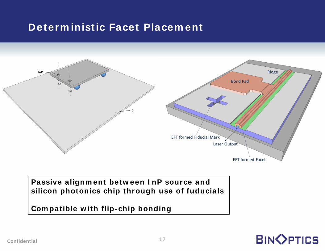
Deterministic Facet Placement
Mechanical cleaving results in typical facet location ±5µm from desired location (at best ±2µm)
Requires active alignment to couple to other components
Facet locations determined by precision of lithography tools
– Better than ±0.1µm
Can couple to other components with passive alignment
Cleaved Facets Etched Facets
Place facets with extreme precision
Eliminates the need to use costly active alignment; allows passive alignment
Confidential 17
Deterministic Facet Placement
Passive alignment between InP source and silicon photonics chip through use of fuducials Compatible with flip-chip bonding
Confidential 18
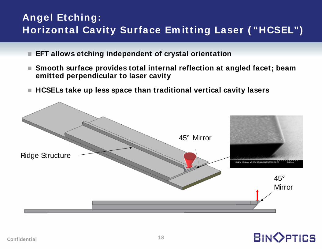
Angel Etching: Horizontal Cavity Surface Emitting Laser (“HCSEL”)
EFT allows etching independent of crystal orientation
Smooth surface provides total internal reflection at angled facet; beam emitted perpendicular to laser cavity
HCSELs take up less space than traditional vertical cavity lasers
45° Mirror
45° Mirror
Ridge Structure

Confidential 19
Low Reflectivity Facets
Etched-facets allow low reflectivity values by using angled facets
A
A = facet tilt angle
ridge
Normal to facet
facet coated with single layer of dielectric coating to give 6% reflectivity at zero facet tilt angle
Simulation
measurements
Low cost RSOA InP sources for silicon photonics
Confidential
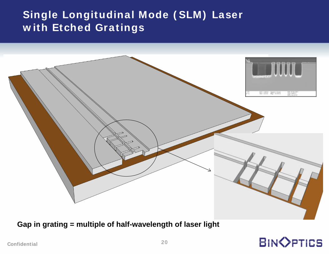
Single Longitudinal Mode (SLM) Laser with Etched Gratings
20
Gap in grating = multiple of half-wavelength of laser light
Confidential
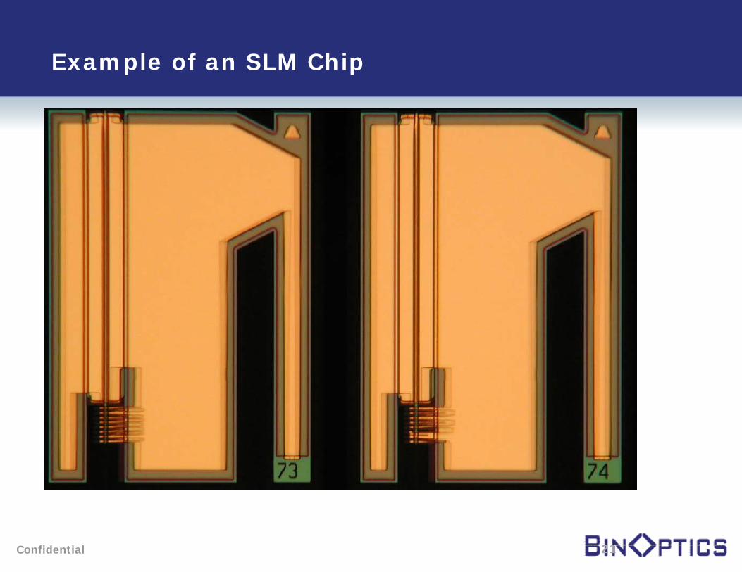
Example of an SLM Chip
21
Confidential
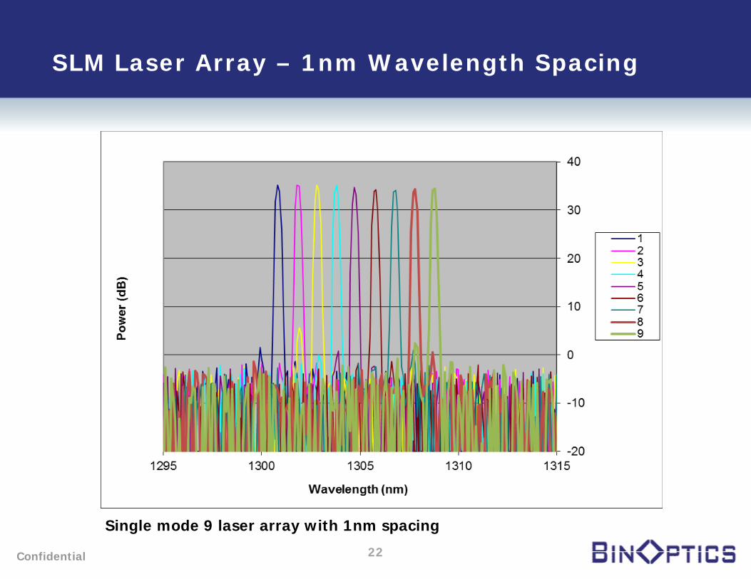
SLM Laser Array – 1nm Wavelength Spacing
22
Single mode 9 laser array with 1nm spacing

Confidential
Operation in Non-Hermetic Environments
Etched Facet Laser Cleaved Facet Laser
23
Etched-facet lasers can operate in non-hermetic environments (direct exposure to temperature and humidity) since there are no exposed semiconductor surfaces to degrade
Passivation on etched facet devices
– Eliminates cost of bulky hermetic packages
– Enables use in new applications
Possibility of delamination in non-hermetic environments
Confidential
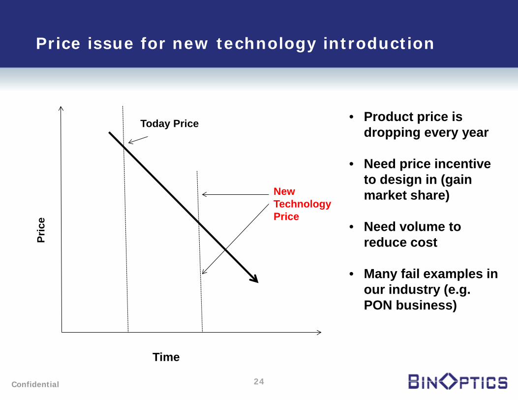
Price issue for new technology introduction
24
Time
Pric
e
Today Price
New Technology Price
• Product price is dropping every year
• Need price incentive to design in (gain market share)
• Need volume to reduce cost
• Many fail examples in our industry (e.g. PON business)
Confidential
New Challenge Ahead
25
• Can we find efficient ways to couple light to Silicon chips
• Can we improve the wall plug efficiency • Can we improve the yield to demonstrate
cost-effectiveness over the old technologies
Confidential
Conclusion
26
PIC vs Si Photonics; Hype or Reality? I believe both the InP base PIC and the Silicon Photonics technologies are real and they are happening Each technology will find their places in theTelecom and Datacom Industries. It depends on the applications