Embed Size (px)
Citation preview

MASTER THESIS
Bc. Marián Betušiak
Effect of the laser pulse illumination on charge collection
efficiency in radiation detectors
Institute of Physics of Charles University
Supervisor of the master thesis: Doc. Ing. Eduard Belas, CSc.
Study programme: Physics
Specialization: Optics and Optoelectronics
Prague 2020

I declare that I carried out this master thesis independently, and only with the cited
sources, literature and other professional sources.
I understand that my work relates to the rights and obligations under the Act No.
121/2000 Coll., the Copyright Act, as amended, in particular the fact that the Charles
University has the right to conclude a license agreement on the use of this work as a
school work pursuant to Section 60 paragraph 1 of the Copyright Act.
In Prague 30.7.2020 signature

2
I would like to thank all employees and students from the Department of
Optoelectronics and Magneto-Optics at the Institute of Physics of Charles University.
Above all, I would like to thank my supervisor doc. Ing. Eduard Belas CSc. for his
guidance and his countless advices during the measurement and writing of this thesis.
I would also like to thank prof. RNDr. Roman Grill CSc.for the tremendous amount
of his time spent discussing the measured data and possible detector models. Lastly
but not least, I want to thank Mgr. Jindřich Pipek for advices how to use the
experimental setup and for the automation of all measurements since doing them
manually would take an ungodly amount of time.

Title: Effect of the laser pulse illumination on charge collection efficiency in
radiation detectors
Author: Bc. Marián Betušiak
Institute: Institute of Physics of Charles University
Supervisor of the master thesis: doc. Ing. Eduard Belas, CSc.
Abstract:
The main focus of this thesis is the characterization of the charge transport in CdZnTe
radiation detectors and the study of the effect of the detector illumination on charge
transport. The transport properties are evaluated using Laser-induced Transient
Current Technique and the Monte Carlo simulation is used for fitting the measured
current waveforms. The properties of the detector prepared from semi-insulating
CdZnTe single crystal with a platinum Schottky contacts were measured in the dark in
the unpolarized and polarized state and under the anode and cathode continuous LED
above-bandgap illumination.
Keywords: Charge generation, Charge collection, Radiation detectors

2
Contents
Introduction .................................................................................................................. 3
1 Theory .................................................................................................................. 5
1.1 Transport equations ....................................................................................... 5
1.2 Charge transport in a planar detector ............................................................ 6
1.2.1 Constant electric field ............................................................................ 8
1.2.2 Linear electric field ................................................................................ 9
1.3 Effects of charge trapping and detrapping................................................... 12
1.3.1 Approximation beyond transit time ..................................................... 15
1.3.2 Trap controlled mobility ...................................................................... 18
1.4 Surface recombination ................................................................................. 18
1.5 Charge collection efficiency ........................................................................ 20
2 Laser-induced Transient Current Technique ...................................................... 21
2.1 Monte Carlo simulation ............................................................................... 24
3 Results and discussion ....................................................................................... 26
3.1 Detector preparation .................................................................................... 26
3.2 I-V characteristics measurement ................................................................. 26
3.3 L-TCT measurement in the dark ................................................................. 27
3.3.1 Measurement in the unpolarized detector ............................................ 28
3.3.2 Measurement in the polarized detector ................................................ 31
3.3.3 Dynamics of the space charge formation in the dark ........................... 33
3.3.4 The CCE in the dark ............................................................................. 36
3.4 Continuous anode illumination ................................................................... 38
3.5 Continuous cathode illumination ................................................................. 42
4 Conclusion ......................................................................................................... 45
5 Bibliography ....................................................................................................... 47
6 List of Figures .................................................................................................... 49
7 List of Tables...................................................................................................... 51
8 List of Symbols and Abbreviations .................................................................... 52

3
Introduction Radiation detectors are used for detection of electromagnetic radiation starting
with infrared through visible and continuing deep in the X-ray and gamma-ray region
or for the detection of ionizing particles. There are many different types of detectors,
but the most common are semiconductor detectors. They directly convert incident
radiation to an electric signal, unlike scintillators that convert incident radiation to
lower energy electromagnetic radiation (UV, visible) and thus require the connection
with photomultipliers. Application of semiconductor detectors is ranging from
astronomy and particle physics to more “everyday” uses like nuclear power plant
inspection, medical imaging or X-ray quality inspection.
In order to create a high-quality X-ray and gamma-ray detector, one must first
choose suitable material in the first place. The main requirements for semiconductor
detectors are resistivity, bandgap, high mobility-lifetime products of charge carriers
and high absorption in a used part of the spectra and with that associated density and
average atomic number.
To obtain a great signal-to-noise ratio the leakage current needs to be as low as
possible. One way to achieve this is the “right kind” of high resistivity - more precisely
high resistivity caused by the low concentration of free carriers. This type of resistivity
is closely tied with the width of the bandgap – the higher the bandgap the lower the
concentration of free carriers and as a bonus the lower the thermal noise. The ideal
bandgap is somewhere between 1.4 -3 eV [1]. Another way of obtaining low leakage
current is achieved in the reverse direction of a p-n junction often used for silicon and
germanium diode detectors.
The best energy resolution is achieved only when all of the photogenerated
carriers are collected at the electrodes before the carriers either recombine or they are
trapped. Therefore, high carrier mobility and carrier lifetime are required.
Lastly, the higher the absorption, the smaller the detectors can get but still retain
the same signal as their less absorptive counterparts. High absorption is also useful
because in some cases the preparation of larger detectors is rather difficult.

4
Table 0.1: Selected properties of Si, Ge, CdZnTe and GaAs [1], [2]
Material Si Ge CdZnTe GaAs
Atomic number 14 32 48, 30, 52 31, 33
Density (g.cm-3) 2.33 5.32 5.78-6.2 5.32
Bandgap (eV) 1.12 0.67 1.5 1.43
Electron mobility 𝜇𝑒 (cm2.V-1.s-1) 1400 3900 1000-1100 8000
Hole mobility 𝜇ℎ (cm2.V-1.s-1) 450 1900 50-80 400
Electron-hole pair generation
energy (eV) 3.6 2.96 4.64 4.2
As can be seen in Table 0.1, germanium has excellent properties (mobility,
density, atomic number) for detector fabrication except for the small bandgap and its
need to be cooled down to the cryogenic temperatures preventing germanium to
become room-temperature detector. In terms of bandgap, silicon is a better candidate
than germanium, with roughly third of the germanium mobility, it is still perfect
material for visible and light X-ray detection, but as the photon energy gets higher the
ability of silicon to absorb incident radiation lowers due to silicon’s low density and
atomic number. While GaAs has high mobility, moderate bandgap and higher density
than silicon, the detector performance is significantly debased by the presence of EL2
centre, that limits the electron lifetime [3].
Since the 1960s the cadmium telluride (CdTe) and cadmium-zinc telluride
(CdZnTe) are regarded as a promising material for room-temperature X-ray and
gamma-ray detectors. Great effort was taken to perfect the crystals growth process,
passivation of the surface and contact preparation but detector polarization still
remains an immense problem. Detector polarization can be induced either by intense
X-ray and 𝛾-ray irradiation [4] or simply by applying a bias to the detector [5].
This thesis aims to characterize charge transport in CdZnTe detectors and to
study the effect of the above-bandgap illumination utilizing a Laser-induced transient
current technique. It can also determine how the additional carrier injection affects the
detector polarization and associated charge collection efficiency.

5
1 Theory
1.1 Transport equations
One of the ways to describe the charge transport in a semiconductor is using
continuity equation
𝜕𝑛
𝜕𝑡=
1
𝑒𝛻 ∙ 𝒋𝒆 + 𝐺𝑅𝑒 , (1.1)
where 𝑛 is the concentration of electrons in a conduction band, 𝑒 is the elementary
charge, 𝐣𝐞 is the electron current density and 𝐺𝑅𝑒 describes the generation and
recombination of the electrons. Current density is defined by drift-diffusion equation
[6]
𝒋𝒆 = 𝑒𝑛𝜇𝑒𝑬 + 𝑒𝐷𝑒𝛻𝑛 + 𝑒𝑆𝑒𝛻𝑇, (1.2)
where 𝜇𝑒 is electron mobility, 𝑬 is the intensity of the applied electric field, T is
absolute thermodynamic temperature, 𝐷𝑒 is the diffusion coefficient given by equation
(1.3) and Se is the Soret coefficient given by equation (1.4).
𝐷𝑒 =𝑘𝐵𝑇
𝑒𝜇𝑒 (1.3)
𝑆𝑒 =𝑘𝐵
𝑒𝑛𝜇𝑒 (1.4)
The first term of equation (1.2) corresponds to the drift in electric field 𝐄, while second
term is the result of diffusion. The third term describes electron transport due to the
gradient of temperature in the material.
Combining equations (1.1) and (1.2) and assuming constant temperature and
carrier mobility we get transport equation for electrons
𝜕𝑛
𝜕𝑡= 𝜇𝑒𝑬. 𝛻𝑛 + 𝜇𝑒𝑛
𝜌
휀+ 𝐷𝑒𝛻2𝑛 + 𝐺𝑅𝑒 , (1.5)
where the differential form of Gauss law [7] was used, ρ is the space charge density in
the detector and 휀 is the permittivity of the material. Similarly, transport equation for
holes can be obtained by switching 𝑒 → −𝑒 and 𝜇𝑒 → −𝜇ℎ.

6
1.2 Charge transport in a planar detector The geometry of the planar detector is shown in Fig. 1.1. Assuming that the
lateral dimensions of the detector are much larger than its width 𝐿, calculations can be
reduced from three spatial dimensions to only one. The detector is illuminated at the
centre of the electrode and laser spot with area 𝑆 is small enough that the
inhomogeneity of the electric field near the edges of the detector can be neglected. We
also assume that the applied electric field 𝐸0 is constant with respect to time or at least
that its change during the charge carrier transit is negligible and that the
photogenerated charge does not affect the local electric field. In case of strong
absorption, irradiation generates electron-hole pairs just under the cathode and they
are immediately separated by the electric field. Electrons are drifting towards the
anode in the positive direction of the z-axis, and holes are almost immediately
collected at the cathode. Some detectors may have a guard ring structure (GR in Fig.
1.1) separated by the resistive layer from the central electrode, to suppress the surface
leakage current.
Fig. 1.1: Simplified geometry of the detector.
Internal electric field 𝑬(𝒓, 𝑡) consisting of the applied electric field 𝑬𝟎(𝑡) and
the electric field induced by space charge 𝑬𝝆(𝒓, 𝑡), can be rewritten as
𝑬(𝒓, 𝑡) = 𝑬𝟎(𝑡) + 𝑬𝝆(𝒓, 𝑡) =𝑈
𝐿𝒛 + 𝐸𝜌(𝑧)𝒛, (1.6)
where 𝑈 is applied bias and 𝒛 is a unit vector in the z-direction. Subsequently, the
equation (1.5) transforms to
𝜕𝑛(𝑧, 𝑡)
𝜕𝑡= 𝜇𝑒 (
𝑈
𝐿+ 𝐸𝜌(𝑧))
𝜕𝑛(𝑧, 𝑡)
𝜕𝑧+
+𝜌(𝑧)
𝜀𝑛(𝑧, 𝑡) + 𝐷𝑒
𝜕2𝑛(𝑧,𝑡)
𝜕𝑧2 + 𝐺𝑅(𝑧, 𝑡).
(1.7)

7
Knowing the concentration of the electrons, the Shockley-Ramo theorem [8] is
used to obtain the shape of the current waveform. In the case of two planar electrodes,
the current induced by the charge 𝑞 moving with the drift velocity 𝑣 is simply given
by
𝐼𝑞(𝑡) =𝑞𝑣(𝑡)
𝐿. (1.8)
The electric current induced by the electron distribution 𝑛(𝑧, 𝑡) is then described by
𝐼𝑛(𝑡) = −𝑒𝑆
𝐿∫ 𝑛(𝑧, 𝑡)𝑣𝑒(𝑧)𝑑𝑧
𝐿
0
=𝜇𝑒𝑒
𝐿∫ 𝑛(𝑧, 𝑡)𝐸(𝑧)𝑑𝑧
𝐿
0
, (1.9)
which in the case of sharply localized electron cloud or constant electric field can be
simplified to
𝐼𝑛(𝑡) = 𝑄0(𝑡)𝑣𝑒(𝑡)
𝐿, (1.10)
where Q0 is the overall moving charge and 𝑣𝑒 is the electron drift velocity.
Photogeneration of the carriers provided by a laser pulse is defined by the
generation recombination term 𝐺𝑅 in equation (1.7). Assuming the attenuation of the
square laser pulse is described by the Lambert-Beer law, the generation term is then
𝐺𝑅(𝑧, 𝑡) =𝑁0
𝑆
𝛼
1 − 𝑒𝑥𝑝(−𝛼𝐿)𝑒𝑥𝑝(−𝛼𝑧)
1
𝑡𝑙𝑎𝑠𝑒𝑟𝜒(𝑡, 0, 𝑡𝑙𝑎𝑠𝑒𝑟), (1.11)
where 𝑁0 is the overall number of photogenerated carriers, 𝑆 is illuminated area, 𝛼 is
the absorption coefficient and 𝑡𝑙𝑎𝑠𝑒𝑟 is the duration of the laser pulse and 𝜒(𝑡, 0, 𝑡𝑙𝑎𝑠𝑒𝑟)
is the boxcar function, that is equal to 1 if 0 ≤ 𝑡 ≤ 𝑡𝑙𝑎𝑠𝑒𝑟 and in all other cases is equal
to 0. Both fractions in the formula (1.11) are just normalizing terms of the respective
distribution. However, using the 𝐺𝑅 in the computation leads to quite complicated and
intricate solutions, that is why in the text below the sharply localized electron cloud
𝑛(𝑧, 0) =𝑁0
𝑆𝛿(𝑧) will often be used as an initial condition instead. This simplification
is, in fact, correct since the laser pulse width has to be short enough (significantly
shorter than current waveform) not to distort the current waveform, essentially
becoming the Dirac delta function in time 𝛿(𝑡). Therefore, the term 𝐺𝑅 can be
excluded and the initial condition
𝑛(𝑧, 0) =𝑁0
𝑆
𝛼
1 − 𝑒𝑥𝑝(−𝛼𝐿)𝑒𝑥𝑝(−𝛼𝑧) (1.12)
can be used. For high absorption coefficient (above bandgap illumination) incident
light is absorbed in the thin region beneath the surface (~1
𝛼), thereupon the spatial

8
dependence of initial carrier distribution can be disregarded and again Dirac delta-
function 𝛿(𝑧) can be used.
1.2.1 Constant electric field
Assuming a constant electric field (𝜌 = 0), no diffusion (𝐷𝑒 = 0) and no
generation or recombination of the carries, equation (1.7) takes on a simple form
𝜕𝑛(𝑧, 𝑡)
𝜕𝑡= 𝜇𝑒𝐸0
𝜕𝑛(𝑧, 𝑡)
𝜕𝑧 (1.13)
The solution of the transport equation (1.13) with initial condition 𝑛(𝑥, 0) = 𝑛0(𝑥) is
𝑛(𝑧, 𝑡) = 𝑛0(𝑧 − 𝑣0𝑡), (1.14)
where 𝑣0 denotes drift velocity of electrons 𝑣0 = −𝜇𝑒𝐸0. Since the finite width of the
detector is introduced only by the Schockley-Ramo theorem (equations (1.9) and
(1.10)), solution (1.14) represents the initial electron distribution drifting endlessly
with the velocity 𝑣.
The shape of the current waveform given by (1.10) is not affected by initial
carrier distribution (assuming all carriers are generated at the same time) until the time
the first electron reaches the anode and overall moving charge in the detector 𝑄0 starts
to decrease. The time it takes charge carrier to pass the width of the detector 𝐿 is called
the default transit time 𝑡𝑟0 and is defined as
𝑡𝑟0 =𝐿
|𝑣0|=
𝐿2
𝜇𝑒|𝑈| (1.15)
For simplification let’s assume initial spatial distribution of electrons to be
Dirac delta function 𝑛0(𝑥) = −𝑄0
𝑒𝑆𝛿(𝑥), the current waveform is then described by
𝐼(𝑡) =𝑄0𝑣0
𝐿𝜒(𝑡, 0, 𝑡𝑟0) =
𝑄0
𝑡𝑟0𝜒(𝑡, 0, 𝑡𝑟0). (1.16)
The boxcar function has appeared due to the electron collection at the anode. The
current waveforms for different drift velocities (different biases) are shown in Fig. 1.2.

9
Fig. 1.2: Normalized current waveforms for different biases. Waveforms are
normalized with respect to the current 𝐼0 and trasit time 𝑡𝑟0 of the 𝑈0 waveform.
1.2.2 Linear electric field
Let’s assume a homogeneously charged detector. The electric field exerted by
the constant space charge 𝜌 can be easily calculated using Gauss law and is given by
𝐸𝜌(𝑧) =𝜌
𝜀𝑧 −
𝜌𝐿
2𝜀. (1.17)
In some cases this electric field Eρ can completely screen out the applied electric field
E0 and the inactive layer is formed and space charge in this region then dissipates [9].
Assuming that the electric field in the inactive layer is zero, the electric field in the
detector is then
𝐸(𝑧) = 𝐸0 𝑚𝑎𝑥 (1 + 𝜌
𝜌𝑚(2
𝑧
𝐿− 1) , 0). (1.18)
where 𝜌𝑚 =2𝜀𝐸0
𝐿 is the space charge density for which the electric field beneath the
cathode 𝐸(0) is equal to zero. Formula (1.18) is also valid for the opposite electrode
configuration. As can be seen in Fig. 1.3a) electric field is nonzero in the whole
detector for −|𝜌𝑚| < 𝜌 < |𝜌𝑚|, in all other cases an inactive layer with the width of
𝑤 = 𝐿
2(1 −
𝜌𝑚
𝜌) is formed. Corresponding space charge is shown Fig. 1.3b). Since
the electric field in the inactive layer is zero, electron-hole pairs generated in this layer
cannot drift and recombine.

10
Fig. 1.3: a) Normalized electric field profile for different values of charge density 𝜌
and b) corresponding profile of the normalized charge density.
The equation (1.7) can be rewritten for the case of the linear electric field by
disregarding the diffusion and generation (recombination) of the charge carriers and
substituting the formula (1.18) for the electric field 𝐸𝜌. Obtained equation is then
given by
𝜕𝑛(𝑧, 𝑡)
𝜕𝑡= 𝜇𝑒 (𝐸0 +
𝜌
휀𝑧 −
𝜌𝐿
2휀)
𝜕𝑛(𝑧, 𝑡)
𝜕𝑧+ 𝜇𝑒
𝜌
휀𝑛(𝑧, 𝑡) (1.19)
Assuming initial condition 𝑛(𝑧, 0) = 𝑛0(𝑧), the solution of (1.19) is
𝑛(𝑧, 𝑡) = 𝑒𝑥𝑝 (𝑡𝜇𝜌
𝜖) 𝑛0 (𝑒𝑥𝑝 (
𝑡𝜇𝜌
𝜖) 𝑧
−𝐿
2[𝑒𝑥𝑝 (
𝑡𝜇𝜌
𝜖) − 1] (1 −
𝜌𝑚
𝜌))
(1.20)
As can be seen from the solution (1.20) the electron distribution changes its
shape in time. The first exponential (in product with initial condition 𝑛0) changes the
“height” of the distribution, while the second exponential (multiplying 𝑧) causes the
broadening or shortening of the initial distribution. This may not be apparent, but if
we choose the initial distribution to be Gaussian, the second exponential can be joined
with variance 𝜎 as can be seen below.
𝑛0(𝑧) =1
𝑆√𝜋𝜎𝑒𝑥𝑝 (−
𝑥2
𝜎2) (1.21)

11
𝑛(𝑧, 𝑡) =1
𝑆√𝜋𝜎𝑒𝑥𝑝 (
𝑡𝜇𝜌
𝜖) 𝑒𝑥𝑝 (−
(𝑧 − 𝛾)2
(𝜎 𝑒𝑥𝑝 (−𝑡𝜇𝜌
𝜖 ))2)
𝛾 =𝐿
2(1 − 𝑒𝑥𝑝 (−
𝑡𝜇𝜌
𝜖)) (1 −
𝜌𝑚
𝜌)
(1.22)
Now we can see that the variance 𝜎′ = σ 𝑒𝑥𝑝 (−𝑡𝜇𝜌
𝜖), changes with time and
therefore, the distribution of electrons is broadening (ρ < 0), shortening (ρ > 0) or
stays the same (ρ = 0). Change of the electron distribution shape is shown in Fig. 1.4.
The 𝑡𝑟 1/2 in Fig. 1.4 represents the time the charge carriers require to get to the half
of the sample.
Fig. 1.4: a) Broadening (ρ < 0) and b) shortening (ρ > 0) of the carrier distribution
due to the non-constant electric field. Distributions are normalized with respect to the
maximum of initial distribution n(0,0) = n0max.
In order to obtain the shape of the current waveform, a sharply localized
electron cloud is assumed and equation (1.10) is used. The final current waveform is
then
𝐼(𝑡) = 𝑄0𝜇𝑒𝐸0 (1 −𝜌
𝜌𝑚) 𝑒𝑥𝑝 (−
𝜇𝑒𝜌
𝜖𝑡) 𝜒(𝑡, 0, 𝑡𝑟), (1.23)
where transit time 𝑡𝑟 is given by
𝑡𝑟 =𝑡𝑟0
2
𝜌𝑚
𝜌𝑙𝑛 (
𝜌𝑚 + 𝜌
𝜌𝑚 − 𝜌), (1.24)
If the charge density is equal to ±ρm then transit time goes to infinity. In both
cases, electrons cannot reach the anode either because they recombine at the anode
(𝜌 ≥ 𝜌𝑚) and no signal is detected or they are stopped in the inactive layer (𝜌 ≤ −𝜌𝑚).
Infinite transit time represents itself as the vanishing of the sharp decrease of the

12
waveform as can be seen in Fig. 1.5. Another effect of space charge is the prolongation
of the transit time – transit time is the shortest in the presence of no space charge and
with the increase of charge density ρ transit time prolongs regardless the sign of the
space charge 𝜌.
Fig. 1.5: Normalized current waveforms calculated for different space charge
distributions 𝜌(𝑧).
1.3 Effects of charge trapping and detrapping The charge collection is significantly influenced by the presence of crystal
defects e.g. impurities or point defects. These defects are often described by the
Shockley-Read-Hall model [10], which is schematically shown in Fig. 1.6.
Disregarding the band-to-band recombination and photo-excitation there are four
processes that can occur – a) capture of the free electron from conduction band by a
defect, b) thermal emission of electron back to the conduction band, c) capture of the
free hole from the valence band by a defect and d) thermal emission a hole back to the
valence band. Rates of processes a)-d) are given by formulas [9],[11]
𝑝𝑎 = 𝑣𝑡ℎ𝑛 𝜎𝑛(𝑁𝑡0 − 𝑁𝑡)𝑛 =
𝑛
𝜏𝑡𝑛, (1.25)
𝑝𝑏 = 𝑣𝑡ℎ𝑛 𝜎𝑛𝑁𝐶 𝑒𝑥𝑝 (−
𝐸𝑡
𝑘𝐵𝑇) 𝑁𝑡 =
𝑁𝑡
𝜏𝑑𝑒 , (1.26)
𝑝𝑐 = 𝑣𝑡ℎ𝑝 𝜎𝑝𝑁𝑡𝑝 =
𝑝
𝜏𝑡ℎ, (1.27)
𝑝𝑑 = 𝑣𝑡ℎ𝑝 𝜎𝑝𝑁𝑉𝑒𝑥𝑝 (−
𝐸𝑔−𝐸𝑡
𝑘𝐵𝑇) (𝑁𝑡0 − 𝑁𝑡) =
𝑁𝑡0−𝑁𝑡
𝜏𝑑ℎ , (1.28)

13
where 𝑣𝑡ℎ𝑛 , 𝜎𝑛 (𝑣𝑡ℎ
𝑝, 𝜎𝑝) are thermal velocity and capture cross-section of electrons
(holes), 𝑁𝑡0 is the concentration of all states of level 𝐸𝑡, 𝑁𝑡 is the concentration of all
occupied states of level 𝐸𝑡, 𝑁𝐶 (𝑁𝑣) is the effective density of states in the conduction
(valence) band, 𝑘𝐵 is Boltzmann constant, 𝑇 is the absolute temperature of the crystal
and 𝐸𝑔 is the bandgap of the semiconductor.
Fig. 1.6: Band diagram of the possible defect described by the Shockley-Read-Hall
model, where 𝐸𝑡 is the energy of trapping center and 𝐸𝑐 (𝐸𝑣) represents conduction
(valence) band and 𝐸𝑔 is the width of the bandgap of the semiconductor.
If the rate of thermal emission of an electron from level 𝐸𝑡 back to the
conduction band (1.26) is much higher than the rate of recombining with a hole (the
rate of hole capture by the defect 𝐸𝑡) (1.27) then the defect 𝐸𝑡 is usually identified as
the trapping centre and processes a) and b) as electron trapping and detrapping,
respectively. Similarly, hole trapping and detrapping are introduced. On the other
hand, if the rate (1.26) is smaller than the rate (1.28) the level 𝐸𝑡 is considered to be
recombination centre. Another classification of trapping centers depends on the rate of
detrapping – if the detrapping time is significantly faster than transit time the trapping
centre is called shallow (due to its distance from conduction or valence band) or deep
trapping centre in the opposite case.
Let’s begin with one shallow trap described by trapping time 𝜏𝑡 (1.25) and
detrapping time 𝜏𝑑 (1.26) and also assume that both trapping and detrapping times are
spatially independent and that their temporal change during the flight of probing
carriers is negligible. The evolution of the trapped 𝑛1 and “free” electrons in the
conduction band 𝑛0 in constant electric field can then be described by differential
equations

14
𝜕𝑛0(𝑧, 𝑡)
𝜕𝑡= −𝑣0
𝜕𝑛0(𝑧, 𝑡)
𝜕𝑧−
𝑛0(𝑧, 𝑡)
𝜏𝑡+
𝑛1(𝑧, 𝑡)
𝜏𝑑 (1.29)
𝜕𝑛1(𝑧, 𝑡)
𝜕𝑡=
𝑛0(𝑧, 𝑡)
𝜏𝑡−
𝑛1(𝑧, 𝑡)
𝜏𝑑 (1.30)
Both equations were obtained from equation (1.7) by disregarding diffusion and
assuming that trapped electrons cannot move. Nevertheless, finding the solution to this
system is difficult, so some discussion is needed. In order to simplify the equation
(1.29) spatial dependence (the first term in equation (1.29)) is neglected. However, the
solution will be valid only for the time smaller than 𝑡𝑟0 (for sharply localized electron
distribution), because until 𝑡𝑟0 all the charge carriers are moving with constant drift
velocity 𝑣0 and after the 𝑡𝑟0 the never-trapped charge carries exit the detector. The
dynamics until this point can be imagined as the two-level system that is slowly
reaching its equilibrium distribution of carries. With this in mind, the equations (1.29)
and (1.30) transform to
𝜕𝑛0(𝑡)
𝜕𝑡= −
𝑛0(𝑡)
𝜏𝑡+
𝑛1(𝑡)
𝜏𝑑, (1.31)
𝜕𝑛1(𝑡)
𝜕𝑡=
𝑛0(𝑡)
𝜏𝑡−
𝑛1(𝑡)
𝜏𝑑, (1.32)
with initial condition 𝑛0(0) = 𝑁0 and 𝑛1(0) = 0. The solution of this system is then
𝑛0(𝑡) =𝑁0
(𝜏𝑡 + 𝜏𝑑)[𝜏𝑡 + 𝜏𝑑 𝑒𝑥𝑝 (−𝑡 (
1
𝜏𝑡+
1
𝜏𝑑))] 𝑡 < 𝑡𝑟0 (1.33)
𝑛1(𝑡) =𝑁0𝜏𝑑
(𝜏𝑡 + 𝜏𝑑)[𝑒𝑥𝑝 (−𝑡 (
1
𝜏𝑡+
1
𝜏𝑑)) − 1] 𝑡 < 𝑡𝑟0 (1.34)
After the application of the Shockley-Ramo theorem (1.10) the shape of the current
waveform is obtained
𝐼(𝑡) = 𝑄0𝑣0
(𝜏𝑡 + 𝜏𝑑)𝐿[𝜏𝑡 + 𝜏𝑑 𝑒𝑥𝑝 (−𝑡 (
1
𝜏𝑡+
1
𝜏𝑑))] 𝑡 < 𝑡𝑟0 (1.35)
For the case of deep trap (𝜏𝑑 → ∞) this waveform can be simplified to purely
exponential form and since no detrapping is taking place, the waveform for 𝑡 > 𝑡𝑟0 is
equal to zero
𝐼(𝑡) = 𝑄0𝑣0
𝐿𝑒𝑥𝑝 (−
𝑡
𝜏𝑡) 𝜒(𝑡, 0, 𝑡𝑟0). (1.36)

15
Current waveforms for different trapping and detrapping times are shown in Fig. 1.7.
Fig. 1.7: Normalized current waveforms a) for different trapping times 𝜏𝑡 and no
detrapping (deep trap) and b) for 𝜏𝑡 = 𝑡𝑟 and different de-trapping times 𝜏𝑑 (shallow
trap).
1.3.1 Approximation beyond transit time
The carrier trapping and subsequent detrapping changes the initial distribution
of charge carriers. Due to this current tail induced by detrapped carriers should be
observed beyond the transit time. As was discussed earlier the analytical solution of
system (1.29), (1.30) beyond transit time does not exist so approximative solution
must be found.
Let’s start again with equations (1.37), but this time we dismiss detrapping and
try to calculate the distribution of trapped carriers 𝑛11(𝑧, 𝑡). The detrapping term in
equation (1.29) is basically an interaction term and ties both equations together, by
eliminating it is possible to solve both gradually.
𝜕𝑛00(𝑧, 𝑡)
𝜕𝑡= −𝑣0
𝜕𝑛00(𝑧, 𝑡)
𝜕𝑧−
𝑛00(𝑧, 𝑡)
𝜏𝑡
𝜕𝑛11(𝑧, 𝑡)
𝜕𝑡=
𝑛00(𝑧, 𝑡)
𝜏𝑡−
𝑛11(𝑧, 𝑡)
𝜏𝑑
(1.37)
Solutions of the system (1.37) are given by
𝑛00(𝑧, 𝑡) =
𝑁0
𝑆𝑒𝑥𝑝 (−
𝑡
𝜏𝑡) 𝛿(𝑧 − 𝑡𝑣0)𝜒(𝑧, 0, 𝐿)𝜃(𝑡) (1.38)
𝑛1
1(𝑧, 𝑡) =𝑁0
𝑆𝑣0𝜏𝑡𝑒𝑥𝑝 (−
𝑧
𝜏𝑡𝑣0) 𝑒𝑥𝑝 (−
𝑡 −𝑧
𝑣0
𝜏𝑑) ×
× 𝜒(𝑧, 0, 𝐿)𝜃(𝑡𝑣0 − 𝑧),
(1.39)

16
where 𝜃(tv0 − z) is Heaviside theta. In the 𝑘-th iteration the distribution of the
(𝑘 − 1)-times trapped carriers is used as detrapping or generation term, as can be seen
in the system below.
𝜕𝑛0𝑘(𝑧, 𝑡)
𝜕𝑡= −𝑣0
𝜕𝑛0𝑘(𝑧, 𝑡)
𝜕𝑧−
𝑛0𝑘(𝑧, 𝑡)
𝜏𝑡+
𝑛1𝑘−1(𝑧, 𝑡)
𝜏𝑑
𝜕𝑛1𝑘+1(𝑧, 𝑡)
𝜕𝑡=
𝑛0𝑘(𝑧, 𝑡)
𝜏𝑡−
𝑛1𝑘+1(𝑧, 𝑡)
𝜏𝑑
(1.40)
The first iteration solution of once detrapped carries n01(z, t) using the equation (1.39)
and the system (1.40) is given by
𝑛01(𝑧, 𝑡) =
𝑧
𝑣0𝜏𝑑𝑛1
1(𝑧, 𝑡) (1.41)
The process of evaluation of the current waveform is the same as before except this
time it is necessary to add all the contributions up (never trapped carriers, once
detrapped, …)
𝐼0(𝑡) = 𝑄0𝑣0
𝐿𝑒𝑥𝑝 (−
𝑡
𝜏𝑡) 𝜒(𝑡, 0, 𝑡𝑟) (1.42)
𝐼1(𝑡) = 𝑄0𝑣0
𝐿
𝜏𝑑𝜏𝑡
(𝜏𝑡 − 𝜏𝑑)2𝑒𝑥𝑝 (−
𝑡
𝜏𝑑) [𝛽(𝑡)𝜒(𝑡, 0, 𝑡𝑟)
+ 𝛽 (𝐿
𝑣0) 𝜃(𝑡 − 𝑡𝑟)]
β(t) = 1 − [1 + 𝑡 (1
τt−
1
τ𝑑)] 𝑒𝑥𝑝 [−𝑡 (
1
τt−
1
τ𝑑)]
(1.43)
As can be seen from (1.43) the tail in the first approximation is exponentially damped
as 𝑒𝑥𝑝 (−𝑡
𝜏𝑑). The first approximation is valid only if the charge carrier is on average
trapped half-times since we are only counting never trapped and once trapped carriers.
With the same logic, the 𝑘-th order approximation is valid if carriers are on average
trapped 𝑘
2-times (
0+1+2+⋯+𝑘
𝑘+1=
𝑘
2). Trapping time can be also defined as an average
time carrier is drifting before it is trapped and de-trapping time as an average time
carrier spends in the trap. Now we can calculate how many times on average carrier is
trapped during flight through the detector 𝑁(𝑡) (until the time 𝑡)
𝑁(𝑡) = 𝑡
𝜏𝑡 + 𝜏𝑑 (1.44)
Knowing this, the 𝑘-th order approximation is valid until the time
𝑡𝑙𝑖𝑚 = 𝑘
2(𝜏𝑡 + 𝜏𝑑). Beyond this time higher-order approximations have to be used.

17
Given the used approach the approximated current waveform will always be lower
than the precise solution, as it can be clearly seen in Fig. 1.8. However, for the case of
the constant electric field, distributions of 𝑘-times detrapped carriers 𝑛0𝑘 can be
summed up and precise solution of the system (1.29) and (1.30) with initial condition
𝑛(𝑧, 0) =𝑁0
𝑆𝛿(𝑧) can be obtained. The result of the summation (computed in Wolfram
Mathematica) is given by
𝑛0(𝑧, 𝑡) = 𝑛00(𝑧, 𝑡) + 𝑛0′(𝑧, 𝑡)
𝑛0′(𝑧, 𝑡) = ∑ 𝑛0𝑘(𝑧, 𝑡)
∞
𝑘=1
𝑛0′(𝑧, 𝑡) =𝑁0
𝑆
√𝑧
𝑣0√𝜏𝑡𝜏𝑑(𝑡𝑣0 − 𝑧)𝑒𝑥𝑝 (−
𝑡
𝜏𝑑−
𝑧
𝑣0(
1
𝜏𝑡−
1
𝜏𝑑))
× 𝐽1 (2√(𝑡𝑣0 − 𝑧)𝑧
𝑣0√𝜏𝑡𝜏𝑑
) 𝜃(𝑡𝑣0 − 𝑧 )𝜒(𝑧, 0, 𝐿)
(1.45)
where J1is the modified Bessel function of the first kind of order one. A similar result
obtained by a different method (probability calculations) was obtained by Tefft [12].
The same approach as above can be used for multiple trapping centres and even for
the non-constant electric field.
Fig. 1.8: a) Comparison of the first-order approximation with the precise analytical
solution (dashed) (1.45) for different average trapping (𝜏𝑡 =1
2𝜏𝑑) and b) convergence
of the higher-order approximations (𝜏𝑡 =1
2𝜏𝑑 =
1
6𝑡𝑟0).

18
1.3.2 Trap controlled mobility As can be seen in Fig. 1.8 b) the presence of a shallow trap can impede the
mobility evaluation since carriers reach the opposite electrode much later than the
default transit time 𝑡𝑟0. In this case, the effective mobility that accounts for trapping
and detrapping phenomena that slow down the carriers is introduced [12], [13]. The
lower limit of the effective mobility can be calculated as the fraction of the time carrier
spends drifting during one trapping cycle (𝜏𝑡 + 𝜏𝑑)
𝜇𝑒𝑓𝑓 = 𝜇0
𝜏𝑡
𝜏𝑡 + 𝜏𝑑 (1.46)
The formula (1.46) is valid only in the case when the density of the free carriers is in
equilibrium with the respective trap. This condition represents the situation when the
number of trapping events 𝑁(𝑡𝑟) ≫ 1. As can clearly be seen in Fig. 1.9a) the effective
mobility is double the drift mobility when trapping and detrapping times are equal, but
only after the steady concentration of free carriers was reached (the flat part of the
waveforms). In Fig. 1.9b) waveforms for different detrapping times are shown clearly
demonstrating formula (1.46).
Fig. 1.9: a) Normalized current waveform with different (de-) trapping (𝜏 = 𝜏𝑡 = 𝜏𝑑)
and b) increase of the transit time 𝑡𝑟 due to the effective mobility (𝜏𝑡 =1
20𝑡𝑟0).
1.4 Surface recombination The photogenerated charge can recombine in the surface layer due to the presence of
surface states. The rate of this recombination is often different than the rate of the
recombination in the bulk material. The effect of the surface can be described by the
velocity of the surface recombination 𝑠. Let’s assume that all carriers are
photogenerated in the thin surface layer and let 𝑝𝑏 be the probability of their transition
into the bulk material. Levi et al. [14] assumed that the ratio of the “bulk” carriers to

19
recombined carriers is equal to the ratio of drift velocity v and the velocity of the
surface recombination [15]
𝑝𝑏
1 − 𝑝𝑏=
𝑣
𝑠. (1.47)
The probability of the carrier entering bulk is then
𝑝𝑏 =1
1 +𝑠𝑣
(1.48)
Since the carrier recombination is taking place in the very thin region, its effect on the
shape of the current waveform can be neglected and only the decrease of the collected
charge 𝑄0 (assuming no trapping) described by the equation (1.49) is observed.
𝑄0(𝐸) =
𝑄00
1 +𝑠
𝜇 𝐸(0)
(1.49)
The Q00 is the photogenerated charge and drift velocity 𝑣 = 𝜇 𝐸(0) was substituted
(assuming that the charge is generated at 𝑧 = 0). Because of this, surface
recombination cannot be recognized from one waveform but bias dependence has to
be measured.
The bias-normalized current waveforms for a constant electric field are shown in Fig.
1.10. Bias-normalization was done to visualize the effect of surface recombination,
since the current is normally linear in bias, as can be seen in equations (1.15) and
(1.16).
Fig. 1.10: Current waveforms normalized by bias for the model a) without surface
recombination and b) with surface recombination
20
1.5 Charge collection efficiency Charge collection efficiency (CCE) is one of the most important parameters for
evaluation of the detector quality, defined as a fraction of collected charge to the
generated charge. For deep-level trapping od the carriers the CCE can be described by
the single carrier Hecht equation (assuming strong absorption and constant electric
field) [16]
𝐶𝐶𝐸 =𝜏
𝑡𝑟[1 − 𝑒𝑥𝑝 (−
𝑡𝑟
𝜏)] , (1.50)
where 𝜏 is the carrier lifetime, or by modified Hecht equation that involves surface
recombination [15]
𝐶𝐶𝐸 =𝜏
𝑡𝑟
1
1 +𝑠𝑣
[1 − 𝑒𝑥𝑝 (−𝑡𝑟
𝜏)] . (1.51)

21
2 Laser-induced Transient Current Technique
The laser-induced transient current technique (L-TCT) belongs to the family of
the Time-of-Flight measurements and is commonly used to evaluate detector
properties e.g. carrier mobility, lifetime, electric field profile in the detector, etc. [17]–
[19]. This method is based on measuring the current response generated by short laser
pulses. Laser pulses create electron-hole pairs, that drifts in an applied electric field to
corresponding electrodes. Due to Shockley-Ramo theorem [8], photogenerated
carriers induce electric current on the electrodes, which is subsequently measured by
an oscilloscope. Using this technique, it is possible to trigger oscilloscope directly to
the laser pulse itself rather than the rising edge of the current pulse as it is in the case
of untriggered sources (alfa, gamma). This allows for faster and easier data acquisition
and as a result higher signal-to-noise ratio. Our experimental setup is shown in Fig.
2.1. Above-bandgap laser pulses (2ns FWHM) are provided by SuperK Compact
Supercontinuum white laser combined with 670nm bandpass filter. The optical part of
the setup is completed with a neutral density filter, which attenuates laser intensity.
High laser intensity leads to more effects, one of which is a plasma effect that
significantly complicates the data processing.
Fig. 2.1: Scheme of our L-TCT setup

22
We are also using masks, placed in front of the detector, to avoid illuminating
edges of the detector. Masks presented in Fig. 2.2, are also used to avoid unintentional
illumination of the area near the guard ring. Guard ring is surrounded by the non-
conducting region that separates the guard ring electrode and central pixel which
effectively minimizes the effect of surface leakage current. The laser is focused at the
centre of the detector forming a 1mm2 spot. For the continuous above-bandgap LED
(660nm) illumination a square mask with roughly 25mm2 was used.
Fig. 2.2: Masking of the detector
As a source of a high voltage source, the Sorensen XG 6001.4 is used combined
with custom-made bias switching unit capable operating at maximal frequency 500Hz
and maximal bias of ±1500V. Both the switching unit and the continuum laser are
controlled by arbitrary function generator Tektronix AFG 3252. By applying pulsed
bias with a sharp rising edge (80μs) and sufficient depolarization time, it is possible to
suppress the effect of dark current polarization and by varying the relative position of
the laser pulse and the rising edge it is possible to observe space charge formation with
great time resolution. Schematics of the relative position of the laser and the bias pulse
are shown in Fig. 2.3. In addition, the shutter is used to temporarily block the laser
beam for the measurement of the background (dark) current. Background can be then
conveniently subtracted from the waveform which eliminates triggered noise and
distortion by the dark current. Oscilloscope (LeCroy WaveRunner 640Zi), arbitrary
function generator, shutter and voltage source are all controlled by computer, allowing
full automation of the measurement.

23
Fig. 2.3: Relative position of bias and laser pulse [20]
Due to low laser intensities, the current response needs to be amplified and only
then it can be recorded by an oscilloscope. However, the use of the amplifier brings
out another problem – the measured data are distorted by the transfer function of the
electronic circuit. To obtain the original signal, the deconvolution method from [21] is
used.
Due to using a detector with a guard-ring contact structure in the anode, there
are four different configurations for L-TCT measurement shown in Fig. 2.4. To simplify
the following text we use abbreviations FSe for measurement of electron signal, while
the full/front side (FS) of the detector is illuminated; GRSh for measurement of hole
signal while guard-ring side (GRS) of the detector is illuminated. The evolution of the
space charge in both of these case is the same since the electric field has the same
direction. Similarly, FSh is the measurement of the hole signal while the FS is
illuminated and GRSe is the measurement of the electron signal while the GRS is
illuminated. L-TCT measured in both polarities can give insight into the properties of
the contacts.
For the transition from FSe to GRSh geometry, it is required to turn the detector
around and switch the bias polarity, due to the design of our electronics setup. If the
detector is also simultaneously LED illuminated, during the FSe to GRSh transition
the LED have to be also removed and plugged back in at the opposite side in order not
to change which electrode is LED illuminated.

24
Fig. 2.4: Experimental setup configuration of the measurement of the
electron (FSe, GRSe) and hole (GRSh, FSh) signals.
2.1 Monte Carlo simulation In many cases solving the transport equation (1.7) is difficult, if one would
assume a system with two trapping centres, the solution would become extremely
complex and beyond the transit time, the analytical solution would not exist at all.
Therefore, for the evaluation of transport properties, Monte Carlo (MC) simulation is
used [18],[22] or drift-diffusion and Poisson equation have to be solved numerically
[9]. We are using one dimensional MC simulation based on [18] with the addition of
arbitrary electric field, diffusion and variable laser pulse parameters (width,
absorption).
For the MC simulation, we use the following assumptions. Firstly, the 𝑁 charge
carriers are randomly generated with their initial position satisfying the Lambert-Beer
law. Probability of the carrier being generated at initial position 𝑧 is [20]
𝑝𝑧(𝑧) =𝛼
1 − 𝑒𝑥𝑝(−𝛼𝐿)𝑒𝑥𝑝(−𝛼𝑧)𝜒(𝑧, 0, 𝐿), (2.1)

25
where the fraction is just the normalization term and 𝜒(𝑧, 0, 𝐿) ensures that the carriers
are generated only inside the detector. Similarly, the probability of carrier generation
by a square laser pulse with the width of 𝑡𝑙𝑎𝑠𝑒𝑟 at the time 𝑡 is given by (2.2). However,
it is possible to use any arbitrary temporal distribution pt.
𝑝𝑡(𝑡) =1
𝑡𝑙𝑎𝑠𝑒𝑟𝜒(𝑡, 0, 𝑡𝑙𝑎𝑠𝑒𝑟). (2.2)
The photogenerated charge 𝑄0 is divided among 𝑁 carriers. The surface recombination
is included by introducing the bias (electric field 𝐸) dependence of 𝑄0(𝐸) described
by equation (1.49).
Each time step δt of the simulation, only the free carriers drifts the distance 𝛿𝑧
𝛿𝑧 = 𝜇𝐸(𝑧)𝛿𝑡 + 𝑢 , (2.3)
where 𝐸(𝑧) is the arbitrary electric field and 𝑢 is the contribution of the carrier
diffusion described by the diffusion coefficient 𝐷 and probability distribution [20]
𝑝𝑢 =1
√4𝜋𝐷𝛿𝑡 𝑒𝑥𝑝 (−
𝑢2
4𝐷𝛿𝑡). (2.4)
The MC current waveforms consist of the contributions of all the carriers, on which
the Shockley-Ramo theorem was applied.
Carrier traps are described by their respective trapping 𝜏𝑡𝑟𝑎𝑝𝑝𝑖𝑛𝑔 and
detrapping time 𝜏𝑑𝑒𝑡𝑟𝑎𝑝𝑝𝑖𝑛𝑔, that defines the probability of carrier (de)trapping in time
step 𝛿𝑡
𝑝(𝑑𝑒)𝑡𝑟𝑎𝑝𝑝𝑖𝑛𝑔 =𝛿𝑡
𝜏(𝑑𝑒)𝑡𝑟𝑎𝑝𝑝𝑖𝑛𝑔. (2.5)
Usually, two trap model (one deep and one shallow trap) is used to describe the
trapping and detrapping phenomena. A detailed description of our MC simulation can
be found in [20].

26
3 Results and discussion
3.1 Detector preparation The detectors for this thesis were provided by Redlen Technologies. The detectors
were prepared by from semi-insulating indium-doped CdZnTe single crystal with 10%
of Zn, which was grown by Traveling Heater Method. Scheme of the used detector
with its physical dimensions is shown in
Fig. 3.1. The planar detector has platinum electrical contacts with a guard ring structure
on one side. The uncontacted surface was coated by an epoxy passivation layer.
Fig. 3.1: Physical dimensions of the detector
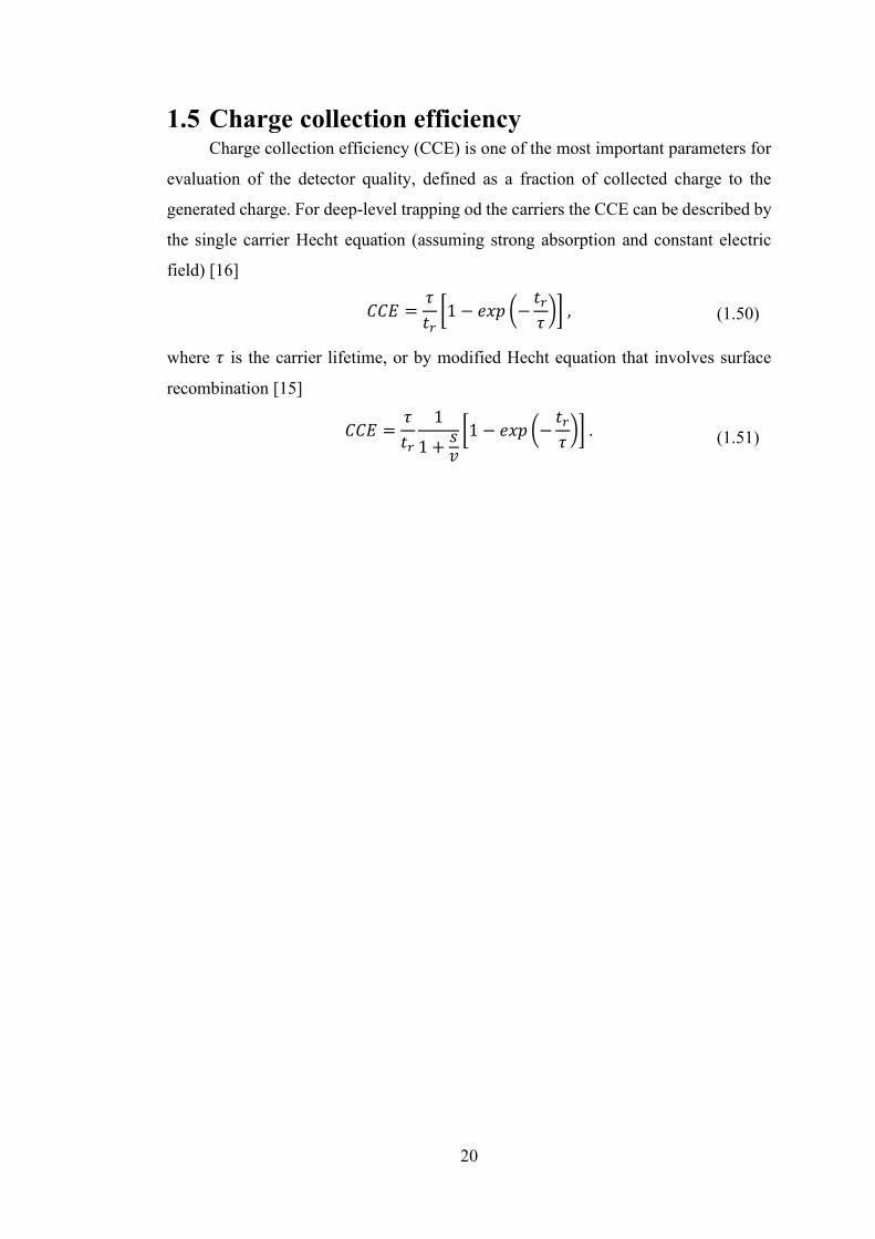
3.2 I-V characteristics measurement The I-V characteristic measurement of Redlen detector curve presented in Fig.
3.2 shows clear rectifying Schottky behaviour with reverse direction for negative bias
applied to the full electrode side (FS). This result was surprising for us because both
electrodes are prepared by the same method using platinum, as was declared by the
vendor. Probably a different (for us) unknown surface treatment was applied for each
side of the detector by Redlen.
27
Fig. 3.2: Current-voltage characteristic. Bias was applied to the full electrode
side (FS). Inset shows detail of the I-V characteristics with negative polarity
3.3 L-TCT measurement in the dark Current waveforms in this thesis were measured only in the FSe or GRSh
geometry (see Fig. 2.4). In both of these, the electric current flows in the negative
direction of 𝑧 axis resulting in negative current in the waveforms. In order to adhere
to the “upward waveform” convention and keep the correct sign of the current, the
waveforms are shown negative side up.
L-TCT was used in the dark (no continuous illumination) and under
continuous LED illumination. Before the L-TCT measurement was done, we had to
find the correct conditions for the measurement of the current waveforms. Firstly, if
we want to measure the unpolarized detector, the laser time delay – LPD (see Fig.
2.3) has to be short enough to acquire the data before the space charge is formed. We
found that for the LPD in the interval 80μs-150μs the current waveforms are the same,
it means that no significant space charge affecting the shape of the waveforms was
formed. For the measurement in the unpolarized detector, the LPD=80μs was chosen.
The second parameter is the depolarization time (DT), which is the bias-off
time in Fig. 2.3. The DT has to be long enough, for the complete depolarization of the
detector. The DT is most reliably measured in the polarized detector when the current

28
waveform is curved and the transit time is sensitive to small variations of charge
density. In the measurement itself 1s wide bias pulse (BPW) and 900ms laser pulse
delay (LPD) was used while a set of waveforms for different DT was measured.
Suitable DTs are the ones, for which the current waveforms are the same. For short
DT the detector does not depolarize completely, therefore the next measured waveform
is affected by the space charge formed during the previous bias pulse. This way the
depolarization time of 100ms was found, but for long-lasting measurements, 500ms
was used to eliminate a chance of a slow space charge build-up.
The third parameter - appropriate laser pulse intensity, was found similarly. A
set of current waveforms was measured for different intensities starting with lowest to
highest. After their comparison, we found the most suitable intensity for L-TCT
measurement. For lower intensities, the current waveforms were lost in the noise and
for higher intensities, they were significantly affected by the plasma effect [23].
3.3.1 Measurement in the unpolarized detector
The unpolarized current waveforms measured in the FSe geometry are
presented in Fig. 3.3. Black dashed lines represent the MC fit. The electric field profile
obtained by the MC simulation is shown in the inset of Fig 3.3. It was found, that
electron waveforms are completely flat in each used bias which points to the fact that
the detector is indeed unpolarized (see subsection 1.2.1). Therefore, an assumption that
for the LPD = 80μs detector is not polarized is correct. The measured electron
waveforms were flat even for -20V so only the lower limit of the electron lifetime was
estimated as 𝜏𝑒 ≫ 2μs (transit time of the -20V waveform).
The hole waveforms measured in the unpolarized detector in GRSh geometry
are shown in Fig. 3.4. The electric field profile obtained by the MC simulation is shown
in the inset in Fig. 3.4 and the fits themselves are displayed as black dashed lines. As
was discussed earlier the electric field in the GRSh geometry is the same as in the FSe,
therefore, the hole waveforms were also measured in the unpolarized detector. Because
of this, the curvature of the hole waveforms can be entirely ascribed to carrier trapping.
Since the hole tails are observed, the two-level model with one deep and one shallow
trap was used for MC fitting. The transport parameters obtained by the MC simulation
are shown in Table 3.1.

29
Fig. 3.3: Pulsed bias dependence of electron current waveforms in FSe geometry using
LPD = 80𝜇𝑠. Black dashed lines represent the fit by MC simulation. Electric field
profile obtained by MC simulation is shown in the inset.
Fig. 3.4: Pulsed bias dependence of the hole current waveforms in GRSh geometry
using LPD = 80𝜇𝑠. Black dashed lines represent the fit by MC simulation. Electric
field profile obtained by MC simulation is shown in the inset.

30
Table 3.1: Transport properties of the unpolarized detector obtained by MC
simulation
Electrons Holes
Carrier mobility
𝜇 (cm2. V−1. s−1) 950 50
Deep level trapping time
𝜏𝑡 𝑑𝑒𝑒𝑝 (μs) ≫ 2 20
Deep level detrapping time
𝜏𝑑 𝑑𝑒𝑒𝑝 (μs)
could not be
evaluated ≫ 10
Shallow level trapping time
𝜏𝑡 𝑠ℎ𝑎𝑙𝑙𝑜𝑤 (μs) ≫ 2 2.7
Shallow level detrapping time
𝜏 𝑑 𝑠ℎ𝑎𝑙𝑙𝑜𝑤 (μs)
could not be
evaluated 3
The bias-normalization of the electron Fig. 3.3 and hole Fig. 3.4 current
waveforms are shown in Fig. 3.5. The individual normalized waveforms have each
different height because some part of the photogenerated carriers recombined in the
surface layer. To evaluate the velocity of the surface recombination of electrons 𝑠𝑒, the
measured current waveforms were firstly integrated to obtain the collected charge.
Bias dependence of the collected charge was then fitted by the equation (1.49) while
the velocity of the surface recombination 𝑠𝑒 and photogenerated charge 𝑄00 were
evaluated.
The velocity of the hole surface recombination, however, could not be
evaluated from the collected charge, because it is also affected by the hole trapping.
The charge that entered bulk (obtained by MC) was used for fitting instead. Obtained
photogenerated charge and surface recombination velocity presented Table 3.2.

31
Fig. 3.5: Bias-normalized pulsed bias dependence of a) electron waveforms in FSe
geometry and b) hole waveforms in GRSh geometry.
Table 3.2: Surface recombination velocity
Electrons Holes
Photogenerated charge
𝑄00 (fC)
135 476
Velocity of the surface recombination
𝑠 (cm. s−1)
5.14
× 105 3.11 × 10⁴
3.3.2 Measurement in the polarized detector
Waveforms in the DC bias regime (polarized detector) were acquired 10
minutes after the biasing. It is necessary to wait until the stabilization of the waveforms
(DC steady-state) or until the waveform evolution is significantly slower than the data
acquisition time. If not, the data would be distorted, since several thousands of
consecutive current waveforms are averaged to increase signal-to-ratio. The electron
and hole waveforms measured in the polarized detector are shown in Fig. 3.6 and
Fig. 3.7, respectively. The MC fit is represented by the black dashed lines and
the electric field profile obtained by MC is shown in the inset. The previously flat
electron waveforms are now increasing in time (see Fig. 3.6 ) and hole waveforms in
Fig. 3.7 are now decreasing more rapidly (than in the unpolarized detector).
Below the -200V formation of the inactive layer beneath the cathode can be seen – in
the case of electrons (Fig. 3.6) no current waveforms can be seen and in the case of
holes (
Fig. 3.7) no apparent transit time is observed. The profile of the fitted electric
field according to the Gauss’s law corresponds to the negative space charge. Linear

32
electric field did not achieve the desired MC fit, so quadratic electric field was used as
a next order Taylor series expansion of the electric field instead. The MC simulation
below −200V could not be evaluated unambiguously – either because there was no
waveform or because there was no observable transit time, by which the effect of
electric field and charge trapping could be distinguished. Carrier mobilities and the
surface recombination velocities obtained in pulsed bias regime were used for DC
regime fitting and only the electric field and the carrier lifetime were fitted in DC. The
deep level trapping time fitted by MC simulation shows significant shortening
compared to the unpolarized detector. The fitted electron lifetime remains still
extremally high. The change of the hole trapping time will be later shown in laser pulse
delay measurement together with the evolution of the space charge.
Fig. 3.6: DC bias dependence of the electron current waveforms in FSe geometry.
Black dashed lines represent the fit by MC simulation. Electric field profile obtained
by MC simulation is shown in the inset.

33
Fig. 3.7: DC bias dependence of the hole current waveforms in GRSh geometry. Black
dashed lines represent the fit by MC simulation. Electric field profile obtained by MC
simulation is shown in the inset.
The formation of the negative space charge can be explained either by the
depletion of holes or injection of electrons. However, hole depletion is more probable
since the material is p-type and data are measured in the reverse direction of Schottky
contact. Another compliant argument is that the slope of the electric field is bigger
beneath the anode than the cathode, which corresponds to more electrons being trapped
beneath the anode 𝑧 = 𝐿 than the cathode 𝑧 = 0. If it was the effect of electron
injection, the charge density would be uniform in the whole detector since extremely
high electron lifetime was measured.
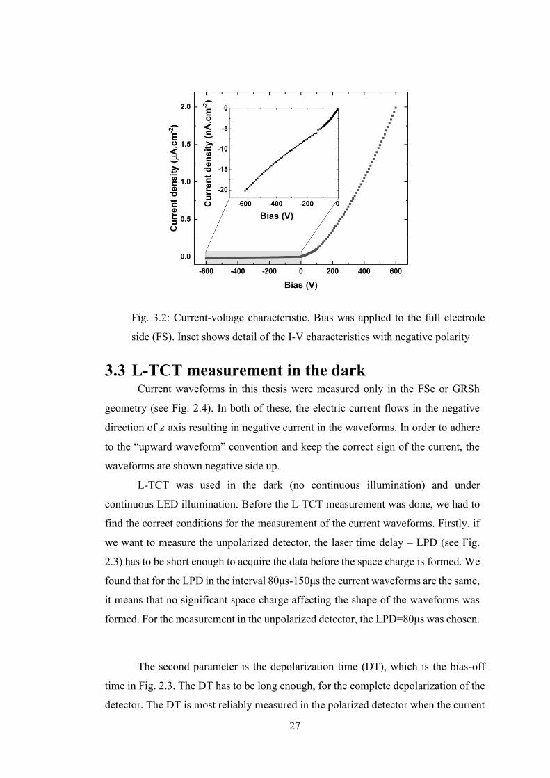
3.3.3 Dynamics of the space charge formation in the dark
Lastly, the temporal evolution of the detector polarization at -400V was
measured by changing the LPD. Waveforms until the LPD = 5s were acquired in the
pulsed bias regime, where one waveform per bias pulse was measured. Any larger
LPDs were measured in DC bias regime, where the mean time of data averaging
(𝑡𝑠𝑡𝑎𝑟𝑡+𝑡𝑒𝑛𝑑
2) was used as a LPD.
The time evolution of electron and hole current waveforms depending on the
laser pulse delay (LPD) are shown in Fig. 3.10 and Fig. 3.9, respectively. Black dashed

34
lines represent the fit by MC simulation and the electric field profile obtained by MC
simulation for each bias is shown in the inset.
The time evolution (LPD) of electron waveforms Fig. 3.8 shows gradual
twisting of the waveforms attributable to the negative space charge build-up. The same
goes for the hole waveforms in Fig. 3.9. The electric field profile in the insets is at first
linear but as the time progresses (LPD) the quadratic term appears. No noticeable
change of electric field was observed until LPD = 1ms and the evolution of the electric
field saturates at LPD = 1h.
Fig. 3.8: Temporal (LPD) evolution of the electron current waveforms measured at
𝑈 = −400𝑉. Black dashed lines represent the fit by MC simulation. Electric field
profile obtained by MC simulation (dashed) is shown in the inset.
35
Fig. 3.9: Temporal (LPD) evolution of the hole current waveforms measured at 𝑈 =
−400𝑉. Black dashed lines represent the fit by MC simulation. Electric field profile
obtained by MC simulation (dashed) is shown in the inset.
Using the MC simulation was found that the electron lifetime is not affected
by the space charge but the lifetime of holes changes significantly. The average charge
density dependence on the LPD is shown in Fig. 3.10 a). The dependence of the hole
deep-level trapping rate (inverse of trapping time) is shown in Fig. 3.10 b). The
trapping rate undoubtedly rises with increasing space charge and one can assume that
the trap responsible for the detector polarization is a hole recombination centre. If the
trap causing the detector polarization is the same as the trap responsible for hole
trapping, then the trapping rate is governed by the formula (1.27) and therefore the
hole trapping rate should be linearly dependent of space charge (concentration of the
occupied trap states). Since it is not the case, there must be another (deep hole) trap
with different capture cross-section – the trap with shorter trapping time will fill faster
than the trap with longer trapping time.

36
Fig. 3.10: a) Temporal (LPD) evolution of the average charge density. b) Dependence
of the trapping rate on the average charge density.
3.3.4 The CCE in the dark
Knowing the photogenerated 𝑄00 and collected charge of electrons and holes,
the charge collection efficiency was evaluated. The electron CCE is affected only by
carrier recombination and therefore was fitted by (1.49). The hole CCE was fitted by
the modified single carrier Hecht relation (1.51). Evaluated CCEs are shown in Fig.
3.11. The hole CCE in polarized DC bias regime is a result of a competition of the
lowering of the hole surface recombination and increasing deep-level trapping rate.
The electric field beneath the anode is increasing due to the negative space charge
thanks to what the hole surface recombination is suppressed on the other side the
presence of the negative space charge increases the deep-level trapping rate.
Eventually, both contributions to CCE partially cancel out.
Fig. 3.11: Dependence of the a) electron and b) hole collection efficiency on the
applied bias in pulsed and DC bias regime. Black lines represent fit by in a) equation
(1.49) and in b) by modified single carrier Hecht equation (1.51).

37
The temporal evolution of the charge collection efficiency is presented in Fig.
3.12. The CCE is decreasing in both cases with LPD. In the case of electrons, the
decrease of the CCE is tied with the decrease of the electric field beneath the cathode
and concurrently amplifying the surface recombination. Collection efficiency of holes
is mainly decreasing due to the measured degradation of the hole lifetime as the
negative space charge builds up. The overshoots in CCE are likely caused by the
decrease of the surface recombination but the exact process is not yet clear and will be
studied more thoroughly in further research.
Fig. 3.12: Temporal evolution (dark) of the a) electron and b) hole collection
efficiency. Dashed lines represent the limit values of CCE measured in pulsed and
DC bias regime with the same voltage applied.

38
3.4 Continuous anode illumination Firstly, the LED intensity dependence of waveforms was measured in DC bias
regime at -400V. Data averaging and detector illumination started only after the biased
detector reached quasi-steady-state (concluded by the current waveforms). After the
measurement was over the bias and LED was turned off allowing the detector to
depolarize and then measurement with different intensity started over. As a result the
electron Fig. 3.13 and hole Fig. 3.14 waveforms were obtained. The LED intensity is
in the figures below displayed as the density of the LED induced photocurrent. The
photocurrent was chosen due to the fact, that the LED and the sample detector had to
be removed in order to switch the measurement geometry (FSe, GRSh) or side of the
LED illumination. After the setup adjustment, the LED could not be aligned perfectly
with its previous position, therefore a slightly different photocurrent was measured for
the same LED intensity (more in section 2).
As seen in the insets of the electric field profile in Fig. 3.13 and Fig. 3.14, with
the increasing photocurrent, the electric field beneath the cathode also rises and
beneath anode decreases. This twisting of the electric field is a result of mitigating the
negative space charge, which for the photocurrent density above - 142nA. cm−2 even
changes sign. The completely flat electron waveform (also has shortest transit time)
shown green in Fig. 3.13 has the same transit time as the waveform measured at -400V
in the unpolarized detector. This suggests that the electric field is for this respective
photocurrent indeed constant. A similar effect was measured for holes at -336nA. cm−2
almost constant electric field and deep level trapping time (25μs) similar to that in the
unpolarized detector (20μs) was obtained by the MC simulation.
For higher photocurrent than -142nA. cm−2 (positive space charge) the
shortening of electron lifetime was observed in Fig. 3.15 b) (grey square). The lifetime
of holes beyond -336nA. cm−2 practically does not change as can be seen in Fig. 3.15
b) (red point). The dependence of the charge density on the density of the photocurrent
in Fig. 3.14 a) is roughly the same for both FSe and GRSh geometries, which suggests
that the LED was returned to a similar position relative to the detector and the mask.

39
Fig. 3.13: LED intensity dependence (illuminated anode) of the electron waveforms
measured in FSe geometry. Black dashed lines represent the fit by MC simulation.
Electric field profile obtained by MC simulation (dashed) is shown in the inset.
Fig. 3.14: LED intensity dependence (illuminated anode) of the hole waveforms
measured in GRSh geometry. Black dashed lines represent the fit by MC simulation.
Electric field profile obtained by MC simulation (dashed) is shown in the inset.

40
In Fig. 3.15 c) and d) the dependence of electron and hole trapping rate is
shown. The trapping rate of electrons is linearly dependent on average charge density
(for positive charge density). The disruption of linear behaviour is caused mostly by
the MC fitting. For negative charge densities, no trapping of electrons was assumed to
simplify the fitting process and for charge density close to zero, the transit time does
not strongly depend on charge density thus a relatively wide range of trapping times
satisfies the fit. Using the same thought process as in the dark measurement, the linear
increase of trapping rate with charge density means that one trap is responsible for
positive space charge build-up and the increase of trapping rate of electrons.
In the case of trapping rate of holes it is hard to describe the dependence since
in the area of interest the data are most affected by the fitting error. But if we look only
at negative charge densities, the dependence is not linear which corresponds to the
measurement in the dark.
Fig. 3.15: a) Dependence of the average charge density on the LED induced
photocurrent. b) Dependence of the trapping rate on the LED induced photocurrent. c)
Dependence of the electron trapping rate on the average charge density.
d) Dependence of the hole trapping rate on the average charge density.

41
The CCE for the measurements above is shown in Fig. 3.16. The electron CCE
rises together with electric field beneath the cathode until the point the surface
recombination is completely suppressed and then saturates. The effect of the
shortening of the electron lifetime is not seen, as it is hidden in the saturation of the
surface recombination. The CCE of holes starts from its (dark) DC bias regime limit,
then reaches a maximum and starts to decrease below the DC limit. We assume that
the maximum is formed by the competition of increasing hole surface recombination
and decreasing hole trapping rate. The maximum is located in the region, where the
trapping rate of holes becomes constant, from this point on the surface recombination
takes over and CCE starts to fall.
Fig. 3.16: Dependence of a) electron and b) hole CCE on the density of the LED
induced photocurrent (illuminated anode)
As was discussed in the previous section, the inactive layer is formed in the
DC bias regime and since anode illumination suppresses the detector polarization, the
flat-electric field bias dependence was also measured. After the DC biasing and the
waveform stabilizing, such LED intensity was set that the measured waveforms were
flat. Fig. 3.17 clearly demonstrates that the LED anode illumination is able to repress
the inactive layer after it is formed. The LED induced photocurrent density required to
flatten the electric field is in the inset compared to the dark current. On average the
photocurrent needs to be 6.6 times the dark current in order to obtain flat electron
waveforms.

42
Fig. 3.17: Flat electric field (continuous LED anode illumination) DC bias dependence
of the current waveforms. Black dashed lines represent the fit by MC simulation.
Corresponding photocurrent density is compared to the dark current density in the
inset.
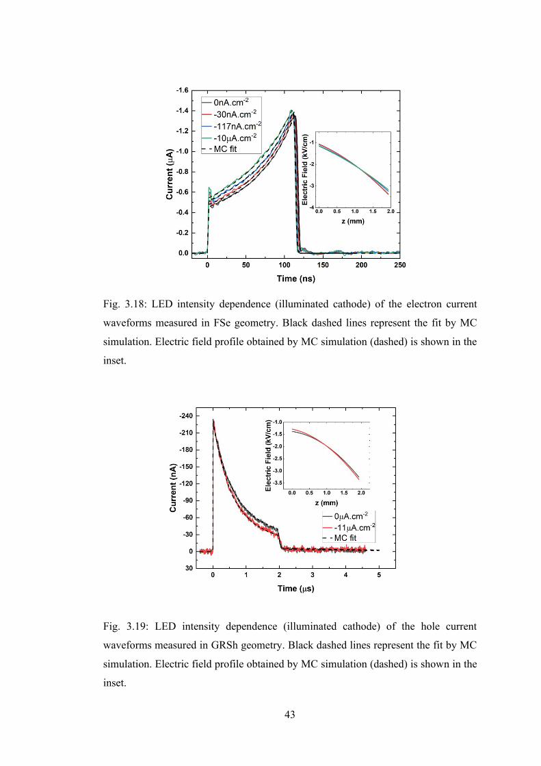
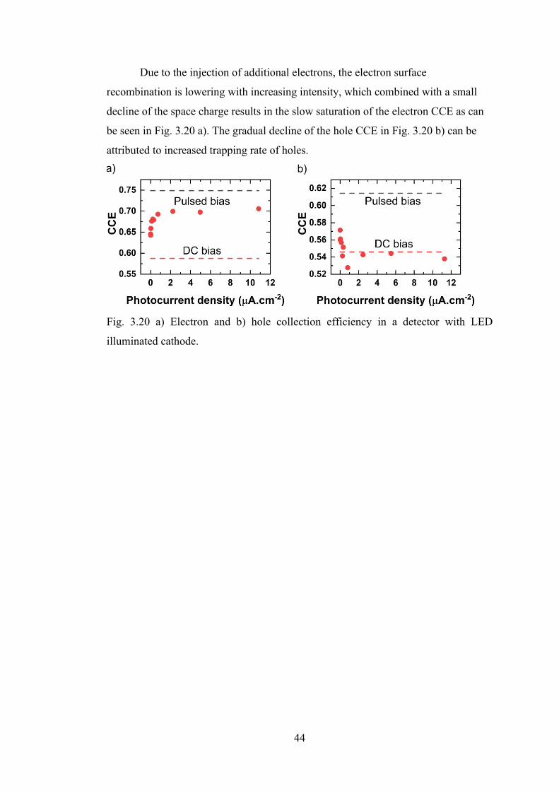
3.5 Continuous cathode illumination Lastly, the illumination of the cathode was studied. The dependence on LED intensity
(induced photocurrent) was measured the same way as for the case of the illuminated
anode. The measured electron and hole signals are shown in Fig. 3.18 and Fig. 3.19
respectively. For better clarity, only the waveforms with visible change are shown in
both figures. This time the illumination induced change was not as significant as for
the anode illumination even though the induced photocurrent was twice that high.
Right after the biased-detector illumination, the electron waveforms shortened and as
the measured dependence displays, the higher the LED intensity the more noticeable
the change. But for high intensities this effect saturates. The shortening of the
waveforms can only be explained by the partial suppression of the negative space
charge since the transit time in the depolarized detector was identical before and after
the illumination. The already built up negative space charge was probably
compensated by the holes that were sucked in from the anode. A decrease of the deep
hole trap was observed from 3μs in the dark to 2μs under the maximal illumination.
43
Fig. 3.18: LED intensity dependence (illuminated cathode) of the electron current
waveforms measured in FSe geometry. Black dashed lines represent the fit by MC
simulation. Electric field profile obtained by MC simulation (dashed) is shown in the
inset.
Fig. 3.19: LED intensity dependence (illuminated cathode) of the hole current
waveforms measured in GRSh geometry. Black dashed lines represent the fit by MC
simulation. Electric field profile obtained by MC simulation (dashed) is shown in the
inset.
44
Due to the injection of additional electrons, the electron surface
recombination is lowering with increasing intensity, which combined with a small
decline of the space charge results in the slow saturation of the electron CCE as can
be seen in Fig. 3.20 a). The gradual decline of the hole CCE in Fig. 3.20 b) can be
attributed to increased trapping rate of holes.
Fig. 3.20 a) Electron and b) hole collection efficiency in a detector with LED
illuminated cathode.

45
4 Conclusion
In this thesis, the detector transport properties were evaluated in the dark and under
continuous LED illumination using the Laser-induced Transient Current Technique
and in-house made Monte Carlo simulation for fitting the measured current
waveforms. In the dark, the electron and hole signals were measured in the unpolarized
and polarized detector. The electron and hole mobility of 𝜇𝑒 = 950 cm2. V−1. s−1 and
𝜇ℎ = 50cm2. V−1. s−1 respectively were determined from the unpolarized current
waveforms. The hole waveforms were fitted by a two-level system of one shallow and
one deep hole trap and the hole lifetime of 11μs was found. The electron lifetime,
however, could not be successfully evaluated as for the -20V no decay of the electron
current waveforms was observed. In the DC bias regime, the current waveforms were
strongly affected by the presence of the negative space charge in the detector. Presence
of this space charge visibly reduced the hole lifetime and corresponding charge
collection efficiency. The electron collection efficiency in the dark detector was only
affected by the surface recombination.
The continuous illumination of the anode led to an increase in charge collection
efficiency of both types of carries until the surface recombination took over and
decrease the CCE of holes. It was also found out that the anode illumination is able to
compensate built-up space charge, change its sign or even eliminate the already formed
inactive layer.
The effect of the illumination of the cathode was much less prominent. The
partial compensation of negative space charge by injected holes was observed. The
exact mechanism of holes injection is not yet understood and will be subjected to
follow-up research.
The negative space charge formation after the biasing, its compensating by the
anode illumination and almost no effect of cathode illumination all point to the fact,
that the detector biased in FSe and GRSh geometry polarizes due to the hole depletion.
Therefore, the anode illumination provides the holes that would otherwise be blocked
by the Schottky contact resulting in suppression of negative space charge formation.
The cathode illumination provides additional electrons but due to their exceptionally
high lifetime, their effect is negligible.

46
Since it was found out that the continuous illumination sufficiently suppresses
the detector polarization only the continuous LED illumination was measured. The
additional illumination by the LED pulses will be the object of our next study.

47
5 Bibliography [1] T. E. Schlesinger and R. B. James, Semiconductors for room temperature nuclear
detector applications. San Diego: Academic Press, 1995.
[2] P. Guerra, D. G. Darambara, D. Visvikis, and A. Santos, “Optimization of a pixellated
CdZnTe/CdTe detector for a multi-modality imaging system,” in 2007 IEEE Nuclear
Science Symposium Conference Record, Honolulu, HI, USA, 2007, pp. 2976–2979,
doi: 10.1109/NSSMIC.2007.4436759.
[3] A. I. Ayzenshtat et al., “GaAs as a material for particle detectors,” Nucl. Instrum.
Methods Phys. Res. Sect. Accel. Spectrometers Detect. Assoc. Equip., vol. 494, no. 1,
pp. 120–127, Nov. 2002, doi: 10.1016/S0168-9002(02)01455-9.
[4] D. Vartsky et al., “Radiation induced polarization in CdTe detectors,” Nucl. Instrum.
Methods Phys. Res. Sect. Accel. Spectrometers Detect. Assoc. Equip., vol. 263, no. 2,
pp. 457–462, Jan. 1988, doi: 10.1016/0168-9002(88)90986-2.
[5] A. Cola and I. Farella, “The polarization mechanism in CdTe Schottky detectors,”
Appl. Phys. Lett., vol. 94, no. 10, p. 102113, Mar. 2009, doi: 10.1063/1.3099051.
[6] J. Franc and P. Höschl, “Fyzika polovodičů pro Optoelektroniku I.” 2014.
[7] R. P. Feynman, R. B. Leighton, and M. Sands, “4-6 Gauss’ law; the divergence of E,”
in The Feynman Lectures on Physics Volume II, New Millenium Edition., Basic Books,
2011.
[8] W. Shockley, “Currents to Conductors Induced by a Moving Point Charge,” J. Appl.
Phys., vol. 9, no. 10, pp. 635–636, Oct. 1938, doi: 10.1063/1.1710367.
[9] R. Grill et al., “Polarization Study of Defect Structure of CdTe Radiation Detectors,”
IEEE Trans. Nucl. Sci., vol. 58, no. 6, pp. 3172–3181, Dec. 2011, doi:
10.1109/TNS.2011.2165730.
[10] W. Shockley and W. T. Read, “Statistics of the Recombinations of Holes and
Electrons,” Phys. Rev., vol. 87, no. 5, pp. 835–842, Sep. 1952, doi:
10.1103/PhysRev.87.835.
[11] L. Reggiani, Hot-Electron Transport in Semiconductors. Springer Berlin Heidelberg,
1985.
[12] W. E. Tefft, “Trapping Effects in Drift Mobility Experiments,” J. Appl. Phys., vol. 38,
no. 13, pp. 5265–5272, Dec. 1967, doi: 10.1063/1.1709312.
[13] K. Suzuki, M. Shorohov, T. Sawada, and S. Seto, “Time-of-Flight Measurements on
TlBr Detectors,” IEEE Trans. Nucl. Sci., vol. 62, no. 2, pp. 433–436, Apr. 2015, doi:
10.1109/TNS.2015.2403279.
[14] A. Levi, M. M. Schieber, and Z. Burshtein, “Carrier surface recombination in HgI 2
photon detectors,” J. Appl. Phys., vol. 54, no. 5, pp. 2472–2476, May 1983, doi:
10.1063/1.332363.
[15] K. Suzuki and H. Shiraki, “Evaluation of surface recombination velocity of CdTe
radiation detectors by time-of-flight measurements,” in 2008 IEEE Nuclear Science
Symposium Conference Record, Oct. 2008, pp. 213–216, doi:
10.1109/NSSMIC.2008.4775165.
[16] K. Hecht, “Zum Mechanismus des lichtelektrischen Primärstromes in isolierenden
Kristallen,” Z. Für Phys., vol. 77, no. 3, pp. 235–245, Mar. 1932, doi:
10.1007/BF01338917.
[17] Š. Uxa, E. Belas, R. Grill, P. Praus, and R. B. James, “Determination of Electric-Field
Profile in CdTe and CdZnTe Detectors Using Transient-Current Technique,” IEEE
Trans. Nucl. Sci., vol. 59, no. 5, pp. 2402–2408, Oct. 2012, doi:
10.1109/TNS.2012.2211615.
[18] K. Suzuki, T. Sawada, and K. Imai, “Effect of DC Bias Field on the Time-of-Flight
Current Waveforms of CdTe and CdZnTe Detectors,” IEEE Trans. Nucl. Sci., vol. 58,
no. 4, pp. 1958–1963, Aug. 2011, doi: 10.1109/TNS.2011.2138719.
[19] J. Fink, H. Krüger, P. Lodomez, and N. Wermes, “Characterization of charge
collection in CdTe and CZT using the transient current technique,” Nucl. Instrum.

48
Methods Phys. Res. Sect. Accel. Spectrometers Detect. Assoc. Equip., vol. 560, no. 2,
pp. 435–443, May 2006, doi: 10.1016/j.nima.2006.01.072.
[20] J. Pipek, “Charge transport in semiconducting radiation detectors,” Charles University,
2018.
[21] P. Praus, E. Belas, J. Bok, R. Grill, and J. Pekárek, “Laser Induced Transient Current
Pulse Shape Formation in (CdZn)Te Detectors,” IEEE Trans. Nucl. Sci., vol. 63, no. 1,
pp. 246–251, Feb. 2016, doi: 10.1109/TNS.2015.2503600.
[22] C. Jacoboni and L. Reggiani, “The Monte Carlo method for the solution of charge
transport in semiconductors with applications to covalent materials,” Rev. Mod. Phys.,
vol. 55, no. 3, pp. 645–705, Jul. 1983, doi: 10.1103/RevModPhys.55.645.
[23] A. V. Tyazhev, V. Novikov, O. Tolbanov, A. Zarubin, M. Fiederle, and E. Hamann,
“Investigation of the current-voltage characteristics, the electric field distribution and
the charge collection efficiency in X-ray sensors based on chromium compensated
gallium arsenide,” Sep. 2014, vol. 9213, p. 92130G, doi: 10.1117/12.2061302.

49
6 List of Figures Fig. 1.1: Simplified geometry of the detector. ............................................................. 6
Fig. 1.2: Normalized current waveforms for different biases. Waveforms are
normalized with respect to the current 𝐼0 and trasit time 𝑡𝑟0 of the 𝑈0 waveform. ..... 9
Fig. 1.3: a) Normalized electric field profile for different values of charge density 𝜌
and b) corresponding profile of the normalized charge density. ................................ 10
Fig. 1.4: a) Broadening ρ < 0 and b) shortening ρ > 0 of the carrier distribution due
to the non-constant electric field. ............................................................................... 11
Fig. 1.5: Normalized current waveforms calculated for different space charge
distributions 𝜌(𝑧). ...................................................................................................... 12
Fig. 1.6: Band diagram of the possible defect described by the Shockley-Read-Hall
model. ......................................................................................................................... 13
Fig. 1.7: Normalized current waveforms a) for different trapping times 𝜏𝑡 and no
detrapping (deep trap) and b) for 𝜏𝑡 = 𝑡𝑟 and different de-trapping times 𝜏𝑑 (shallow
trap). ........................................................................................................................... 15
Fig. 1.8: a) Comparison of the first-order approximation with the precise analytical
solution (1.45) for different average trapping and b) convergence of the higher-order
approximations. .......................................................................................................... 17
Fig. 1.9: a) Normalized current waveform with different (de-) trapping and b)
increase of the transit time 𝑡𝑟 due to the effective mobility ....................................... 18
Fig. 1.10: Current waveforms normalized by bias for the model a) without surface
recombination and b) with surface recombination ..................................................... 19
Fig. 2.1: Scheme of our L-TCT setup ........................................................................ 21
Fig. 2.2: Masking of the detector ............................................................................... 22
Fig. 2.3: Relative position of bias and laser pulse [20] .............................................. 23
Fig. 2.4: Experimental setup configuration of the measurement of the electron and
hole signals. ................................................................................................................ 24
Fig. 3.1: Physical dimensions of the detector ............................................................ 26
Fig. 3.2: Current-voltage characteristic. Bias was applied to the full electrode side
(FS). Inset shows detail of the I-V characteristics with negative polarity ................. 27
Fig. 3.3: Pulsed bias dependence of electron current waveforms in FSe geometry ... 29
Fig. 3.4: Pulsed bias dependence of the hole current waveforms in GRSh geometry 29

50
Fig. 3.5: Bias-normalized pulsed bias dependence of a) electron waveforms in FSe
geometry and b) hole waveforms in GRSh geometry. ............................................... 31
Fig. 3.6: DC bias dependence of the electron current waveforms. ............................ 32
Fig. 3.7: DC bias dependence of the hole current waveforms. .................................. 33
Fig. 3.8: Temporal evolution of the electron current waveforms .............................. 34
Fig. 3.9: Temporal evolution of the hole current waveforms .................................... 35
Fig. 3.10: a) Temporal evolution of the average charge density. b) Dependence of the
trapping rate on the average charge density. .............................................................. 36
Fig. 3.11: Dependence of the a) electron and b) hole collection efficiency on the
applied bias in pulsed and DC bias regime. ............................................................... 36
Fig. 3.12: Temporal evolution of the a) electron and b) hole collection efficiency. .. 37
Fig. 3.13: LED intensity dependence (illuminated anode) of the electron waveforms
measured in FSe geometry.. ....................................................................................... 39
Fig. 3.14: LED intensity dependence (illuminated anode) of the hole waveforms
measured in GRSh geometry. .................................................................................... 39
Fig. 3.15: a) Dependence of the average charge density on the LED induced
photocurrent. b) Dependence of the trapping rate on the LED induced photocurrent.
c) Dependence of the electron trapping rate on the average charge density.
d) Dependence of the hole trapping rate on the average charge density. ................... 40
Fig. 3.16: Dependence of a) electron and b) hole CCE on the density of the LED
induced photocurrent (illuminated anode) ................................................................. 41
Fig. 3.17: Flat electric field (continuous LED anode illumination) DC bias
dependence of the current waveforms........................................................................ 42
Fig. 3.18: LED intensity dependence (illuminated cathode) of the electron current
waveforms measured in FSe geometry. ..................................................................... 43
Fig. 3.19: LED intensity dependence (illuminated cathode) of the hole current
waveforms measured in GRSh geometry. .................................................................. 43
Fig. 3.20 a) Electron and b) hole collection efficiency in a detector with LED
illuminated cathode. ................................................................................................... 44

51
7 List of Tables Table 0.1: Selected properties of Si, Ge, CdZnTe and GaAs ..................................... 4
Table 3.1: Transport properties of the unpolarized detector obtained by MC
simulation ................................................................................................................... 30
Table 3.2: Surface recombination velocity ................................................................ 31

52
8 List of Symbols and Abbreviations 𝛼 absorption coefficient
𝐵𝑃𝑊 bias pulse width
𝛿(𝑧) Dirac delta function
𝐶𝐶𝐸 charge collection efficiency (definition in section 1.5)
𝐷𝑒 , 𝐷ℎ electron and hole diffusion coefficient
𝐷𝑇 depolarization time
𝑒 elementary charge
휀 permittivity of the material
𝐸(𝑧, 𝑡) electric field
𝐸0(𝑧, 𝑡) applied electric field
𝐸𝑔 with of the bandgap
𝐸𝜌(𝑧, 𝑡) electric field exerted by the charge density 𝜌
𝐸𝑡 the energy of the trapping centre in the bandgap
𝐹𝑆 full electrode side of the detector
𝐹𝑆𝑒, 𝐹𝑆ℎ measurement of electron and hole signal from 𝐹𝑆 (more in Fig. 2.4)
𝐺𝑅 guard ring
𝐺𝑅𝑆 guard ring side of the detector
𝐺𝑅𝑆𝑒, 𝐺𝑅𝑆ℎ measurement of electron and hole signal form 𝐺𝑅𝑆 (more in Fig. 2.4)
𝜒(𝑡, 𝑡1, 𝑡2) boxcar function, 𝜒(𝑡, 𝑡1, 𝑡2) = 1 for 𝑡1 ≤ 𝑡 ≤ 𝑡2 else 𝜒(𝑡, 𝑡1, 𝑡2) = 0
𝐼(𝑡) the electric current measured as a current waveform
𝐽1(𝑧) modified Bessel function of the first kind of order one
𝑗𝑒 , 𝑗ℎ electron and hole current density
𝑘𝐵 Boltzmann constant
𝐿 width of the detector
𝐿 − 𝑇𝐶𝑇 Laser-induced Transient Current Technique
𝐿𝑃𝐷 laser pulse delay (relative to the rising edge of the bias pulse)
𝑀𝐶 Monte Carlo simulation
𝜇𝑒 , 𝜇ℎ electron and hole mobility
𝜇𝑒𝑓𝑓 effective mobility
𝑛(𝑧, 𝑡) the density of free electrons in the conduction band
𝑛0, 𝑛00, 𝑛0
𝑘 the concentration of the free electrons, never trapped electrons and 𝑘-
times detrapped electrons
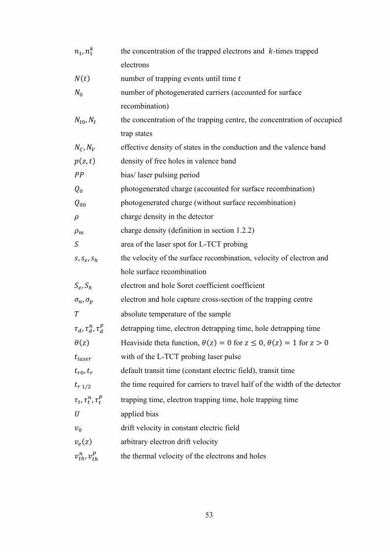
53
𝑛1, 𝑛1𝑘 the concentration of the trapped electrons and 𝑘-times trapped
electrons
𝑁(𝑡) number of trapping events until time 𝑡
𝑁0 number of photogenerated carriers (accounted for surface
recombination)
𝑁𝑡0, 𝑁𝑡 the concentration of the trapping centre, the concentration of occupied
trap states
𝑁𝐶 , 𝑁𝑉 effective density of states in the conduction and the valence band
𝑝(𝑧, 𝑡) density of free holes in valence band
𝑃𝑃 bias/ laser pulsing period
𝑄0 photogenerated charge (accounted for surface recombination)
𝑄00 photogenerated charge (without surface recombination)
𝜌 charge density in the detector
𝜌𝑚 charge density (definition in section 1.2.2)
𝑆 area of the laser spot for L-TCT probing
𝑠, 𝑠𝑒 , 𝑠ℎ the velocity of the surface recombination, velocity of electron and
hole surface recombination
𝑆𝑒 , 𝑆ℎ electron and hole Soret coefficient coefficient
𝜎𝑛, 𝜎𝑝 electron and hole capture cross-section of the trapping centre
𝑇 absolute temperature of the sample
𝜏𝑑 , 𝜏𝑑𝑛, 𝜏𝑑
𝑝 detrapping time, electron detrapping time, hole detrapping time
𝜃(𝑧) Heaviside theta function, 𝜃(𝑧) = 0 for 𝑧 ≤ 0, 𝜃(𝑧) = 1 for 𝑧 > 0
𝑡𝑙𝑎𝑠𝑒𝑟 with of the L-TCT probing laser pulse
𝑡𝑟0, 𝑡𝑟 default transit time (constant electric field), transit time
𝑡𝑟 1/2 the time required for carriers to travel half of the width of the detector
𝜏𝑡, 𝜏𝑡𝑛, 𝜏𝑡
𝑝 trapping time, electron trapping time, hole trapping time
𝑈 applied bias
𝑣0 drift velocity in constant electric field
𝑣𝑒(𝑧) arbitrary electron drift velocity
𝑣𝑡ℎ𝑛 , 𝑣𝑡ℎ
𝑝 the thermal velocity of the electrons and holes