Embed Size (px)
Citation preview
Electronics
An Ultra-Linear LNA for Basestations
Sanganagouda B Patil
Mas
tero
fScie
nce
Thes
is

An Ultra-Linear LNA for Base stations
MASTER OF SCIENCE THESIS
For the degree of Master of Science in Electrical Engineering atDelft University of Technology
Sanganagouda B Patil
November 28, 2013
Faculty of Electrical Engineering, Mathematics and Computer Science (EWI) · Delft Universityof Technology

Copyright c© (Electrical Engineering)All rights reserved.
DELFT UNIVERSITY OF TECHNOLOGY
DEPARTMENT OF
(ELECTRICAL ENGINEERING)
The undersigned hereby certify that they have read and recommend to theFaculty of Electrical Engineering, Mathematics and Computer Science (EWI)
for acceptance a thesis entitled
AN ULTRA-LINEAR LNA FOR BASE STATIONS
by
SANGANAGOUDA B PATIL
in partial fulfillment of the requirements for the degree of
MASTER OF SCIENCE ELECTRICAL ENGINEERING
Dated: November 28, 2013
Supervisor(s):dr. Leo de Vreede
prof. dr. Domine Leenaerts
Ir. Paul Mattheijssen
Reader(s):prof. dr. Kofi A.A. Makinwa

Abstract
In the commercial basestation market of today, LNAs are implemented using GaAs pHEMTtechnology. The popularity of GaAs pHEMT technology is based on its excellent low noise andhigh linearity properties. In this project, an LNA for basestation applications is designed usingSiGe technology, which can provide low noise performance, but requires more work to achievea competitive linearity when comparing with GaAs pHEMT technology. The main motivationof a LNA implementation in SiGe are the lower cost, higher integration possibilities than GaAs.As such, in this master project an ultra-linear LNA has been designed in QUBiC4Xi technologyfor base station applications in the 1710-1980 MHz band.
The requirement for a base station LNA are low noise, high gain, and high linearity. To achievethese goals simultaneously, a 2-stage topology is used where the first stage is optimized for low-noise and high-gain operation, whereas the second stage aims for high linearity and a high 1dBcompression point using negative feedback. The first stage is using a cascode topology, whichprovides high gain and excellent reverse isolation. Its noise figure has been optimized by properbiasing and noise matching.
The output stage is implemented using a differential structure, to enhance linearity and outputpower handling. The techniques used to improve the linearity of the output stage include overallfeedback, Implicit IM3 cancellation, 2nd harmonic termination at the output, and out-of-bandmatching at its output. The out-of-band matching technique has been also evaluated separatelyfor its linearity potential using a simplified Gummel Poon model to understand the impact ofindividual transistor parasitic (C je, τ f , C jc) on linearity.
Since the targeted LNA input and output are single-ended, balun have been used in the interstageconnection and at output convert from single-ended to differential. The 1 dB compression pointof the output stage, which is typically limited by the maximum voltage swing of the transistortechnology is in its configuration enhanced by applying impedance transformation in the outputbalun.
Master of Science Thesis i Sanganagouda B Patil
ii
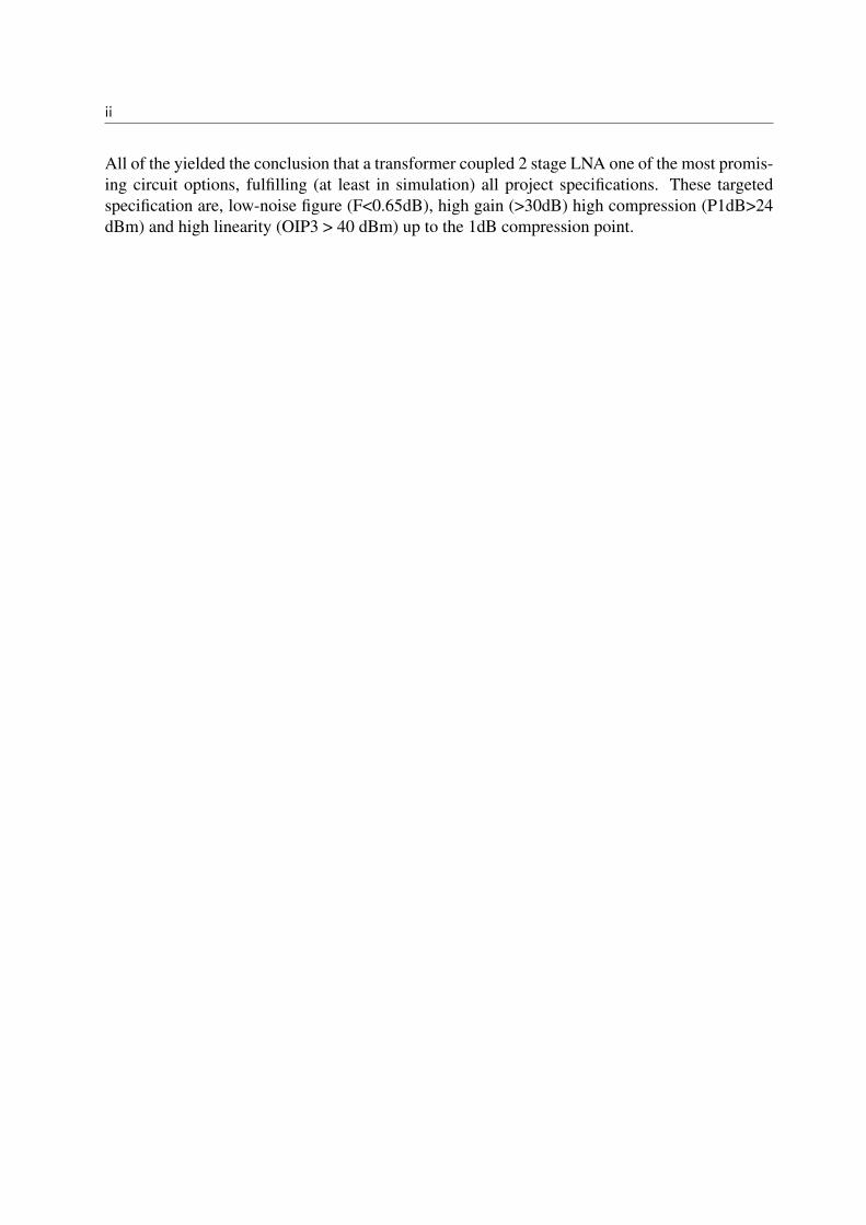
All of the yielded the conclusion that a transformer coupled 2 stage LNA one of the most promis-ing circuit options, fulfilling (at least in simulation) all project specifications. These targetedspecification are, low-noise figure (F<0.65dB), high gain (>30dB) high compression (P1dB>24dBm) and high linearity (OIP3 > 40 dBm) up to the 1dB compression point.

Table of Contents
1 Introduction 11-1 Receiver architecture . . . . . . . . . . . . . . . . . . . . . . . . . . . . . . . 11-2 Requirements for base station LNA . . . . . . . . . . . . . . . . . . . . . . . 21-3 Technologies for LNA . . . . . . . . . . . . . . . . . . . . . . . . . . . . . . 31-4 Motivation and objectives . . . . . . . . . . . . . . . . . . . . . . . . . . . . 41-5 Specifications . . . . . . . . . . . . . . . . . . . . . . . . . . . . . . . . . . 61-6 Thesis organization . . . . . . . . . . . . . . . . . . . . . . . . . . . . . . . 7
2 Low noise amplifier 92-1 Introduction . . . . . . . . . . . . . . . . . . . . . . . . . . . . . . . . . . . 92-2 Two stage approach . . . . . . . . . . . . . . . . . . . . . . . . . . . . . . . 92-3 Negative feedback . . . . . . . . . . . . . . . . . . . . . . . . . . . . . . . . 12
2-3-1 Local feedback . . . . . . . . . . . . . . . . . . . . . . . . . . . . . . 132-3-2 Stability . . . . . . . . . . . . . . . . . . . . . . . . . . . . . . . . . 14
2-4 Two stage design . . . . . . . . . . . . . . . . . . . . . . . . . . . . . . . . . 162-4-1 Differential output stage . . . . . . . . . . . . . . . . . . . . . . . . . 172-4-2 Transformer . . . . . . . . . . . . . . . . . . . . . . . . . . . . . . . 18
2-5 Conclusion . . . . . . . . . . . . . . . . . . . . . . . . . . . . . . . . . . . . 20
3 Linearity enhancement techniques 213-1 Introduction . . . . . . . . . . . . . . . . . . . . . . . . . . . . . . . . . . . 213-2 Device characteristics . . . . . . . . . . . . . . . . . . . . . . . . . . . . . . 21
3-2-1 DC characteristics . . . . . . . . . . . . . . . . . . . . . . . . . . . . 223-2-2 Small signal model . . . . . . . . . . . . . . . . . . . . . . . . . . . . 23
Master of Science Thesis iii Sanganagouda B Patil
iv Table of Contents
3-3 Dominant non-linearities . . . . . . . . . . . . . . . . . . . . . . . . . . . . . 253-4 Techniques to improve linearity . . . . . . . . . . . . . . . . . . . . . . . . . 27
3-4-1 Implicit IM3 cancellation . . . . . . . . . . . . . . . . . . . . . . . . . 27
3-4-2 Out of band linearization . . . . . . . . . . . . . . . . . . . . . . . . 29
3-4-3 2nd harmonic short . . . . . . . . . . . . . . . . . . . . . . . . . . . . 333-5 OP1dB consideration . . . . . . . . . . . . . . . . . . . . . . . . . . . . . . 353-6 Simulation results . . . . . . . . . . . . . . . . . . . . . . . . . . . . . . . . 36
3-6-1 Base tuning . . . . . . . . . . . . . . . . . . . . . . . . . . . . . . . 36
3-6-2 Emitter tuning . . . . . . . . . . . . . . . . . . . . . . . . . . . . . . 42
3-6-3 Discussion . . . . . . . . . . . . . . . . . . . . . . . . . . . . . . . . 453-7 Conclusion . . . . . . . . . . . . . . . . . . . . . . . . . . . . . . . . . . . . 47
4 A two stage low noise and highly linear LNA 494-1 Introduction . . . . . . . . . . . . . . . . . . . . . . . . . . . . . . . . . . . 494-2 Input stage . . . . . . . . . . . . . . . . . . . . . . . . . . . . . . . . . . . . 49
4-2-1 Input impedance and noise matching . . . . . . . . . . . . . . . . . . 50
4-3 Output stage . . . . . . . . . . . . . . . . . . . . . . . . . . . . . . . . . . . 54
4-3-1 Differential cascode stage . . . . . . . . . . . . . . . . . . . . . . . . 56
4-3-2 Differential CE stage . . . . . . . . . . . . . . . . . . . . . . . . . . . 59
4-4 First and second stage combined . . . . . . . . . . . . . . . . . . . . . . . . 63
4-4-1 LNA with differential cascode output stage . . . . . . . . . . . . . . . 63
4-4-2 LNA with differential CE stage output stage . . . . . . . . . . . . . . 66
4-5 Conclusions . . . . . . . . . . . . . . . . . . . . . . . . . . . . . . . . . . . . 68
5 Physical layout and post-layout results 715-1 Introduction . . . . . . . . . . . . . . . . . . . . . . . . . . . . . . . . . . . 715-2 Schematic . . . . . . . . . . . . . . . . . . . . . . . . . . . . . . . . . . . . 715-3 Metal stack . . . . . . . . . . . . . . . . . . . . . . . . . . . . . . . . . . . 725-4 Inductor and balun . . . . . . . . . . . . . . . . . . . . . . . . . . . . . . . . 735-5 Layout considerations . . . . . . . . . . . . . . . . . . . . . . . . . . . . . . 75
5-5-1 Momentum simulation . . . . . . . . . . . . . . . . . . . . . . . . . . 785-6 Post layout simulation results . . . . . . . . . . . . . . . . . . . . . . . . . . 78
5-7 Comparison and conclusion . . . . . . . . . . . . . . . . . . . . . . . . . . . 83
6 Conclusions and future work 856-1 Conclusion . . . . . . . . . . . . . . . . . . . . . . . . . . . . . . . . . . . . 856-2 Future work . . . . . . . . . . . . . . . . . . . . . . . . . . . . . . . . . . . 86

Table of Contents v
A Appendix A 89A-1 Single-ended output stage . . . . . . . . . . . . . . . . . . . . . . . . . . . . 89
A-1-1 An inductively degenerated CE stage . . . . . . . . . . . . . . . . . . 89A-1-2 An inductively degenerated cascode . . . . . . . . . . . . . . . . . . . 91A-1-3 An inductive degenerated cascode with feedback . . . . . . . . . . . . 93
Bibliography 97
Glossary 101List of Acronyms . . . . . . . . . . . . . . . . . . . . . . . . . . . . . . . . . 101

vi Table of Contents
List of Figures
1-1 Receiver Architecture . . . . . . . . . . . . . . . . . . . . . . . . . . . . . . 21-2 Base Station . . . . . . . . . . . . . . . . . . . . . . . . . . . . . . . . . . . 3
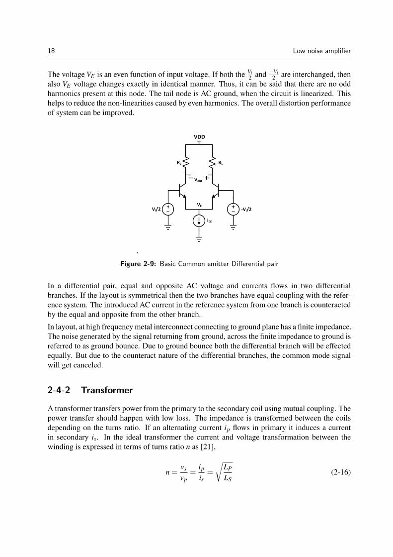
2-1 Two stage approach . . . . . . . . . . . . . . . . . . . . . . . . . . . . . . . 102-2 Noise figure of cascade system . . . . . . . . . . . . . . . . . . . . . . . . . . 102-3 Cascaded blocks . . . . . . . . . . . . . . . . . . . . . . . . . . . . . . . . . 112-4 Overall negative feedback . . . . . . . . . . . . . . . . . . . . . . . . . . . . 122-5 Local feedback . . . . . . . . . . . . . . . . . . . . . . . . . . . . . . . . . . 142-6 Root locus after applying phantom zero . . . . . . . . . . . . . . . . . . . . . 152-7 Dual loop feedback amplifier . . . . . . . . . . . . . . . . . . . . . . . . . . . 162-8 Two stage design . . . . . . . . . . . . . . . . . . . . . . . . . . . . . . . . . 172-9 Basic Common emitter Differential pair . . . . . . . . . . . . . . . . . . . . . 18
3-1 IC vs. VCE characteristic for constant values of VBE , for size 0.3 µm x 1 µm x1 QUBiC4Xi SiGe BNY BJT . . . . . . . . . . . . . . . . . . . . . . . . . . . 22
3-2 IC vs VCE characteristic for constant values of VBE , for size 0.4 µm x 1 µm x 1QUBiC4Xi SiGe BNA BJT . . . . . . . . . . . . . . . . . . . . . . . . . . . . 22
3-3 Small signal model of BJT . . . . . . . . . . . . . . . . . . . . . . . . . . . . 233-4 Simplified small signal model of BJT . . . . . . . . . . . . . . . . . . . . . . 233-5 ft and fmax is simulated for IC vs. VCE of 0 V, for size:0.3 µm x 1 µm x 1
QUBiC4Xi SiGe BNY BJT . . . . . . . . . . . . . . . . . . . . . . . . . . . . 243-6 ft and fmax is simulated for IC vs VCE of 0 V, for size:0.4 µm x 1 µm x 1
QUBiC4Xi SiGe BNA BJT . . . . . . . . . . . . . . . . . . . . . . . . . . . . 253-7 Reference circuit for distortion characterization . . . . . . . . . . . . . . . . 263-8 OIP3-contours in dBm on the IC(VCE) plane at 1.84 GHz of the 0.4µm x 20.7µm
x 1 QUBiC4Xi SiGe BNA transistor . . . . . . . . . . . . . . . . . . . . . . . 26
Master of Science Thesis vii Sanganagouda B Patil
viii List of Figures
3-9 Common emitter transconductance stage model . . . . . . . . . . . . . . . . 28
3-10 Inductive degenerative implicit IM3 cancellation [27] . . . . . . . . . . . . . . 29
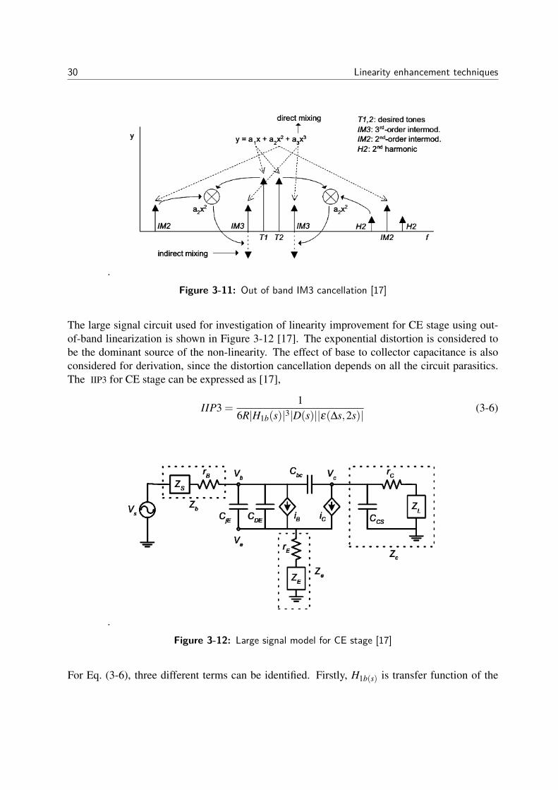
3-11 Out of band IM3 cancellation [17] . . . . . . . . . . . . . . . . . . . . . . . . 30
3-12 Large signal model for CE stage [17] . . . . . . . . . . . . . . . . . . . . . . 30
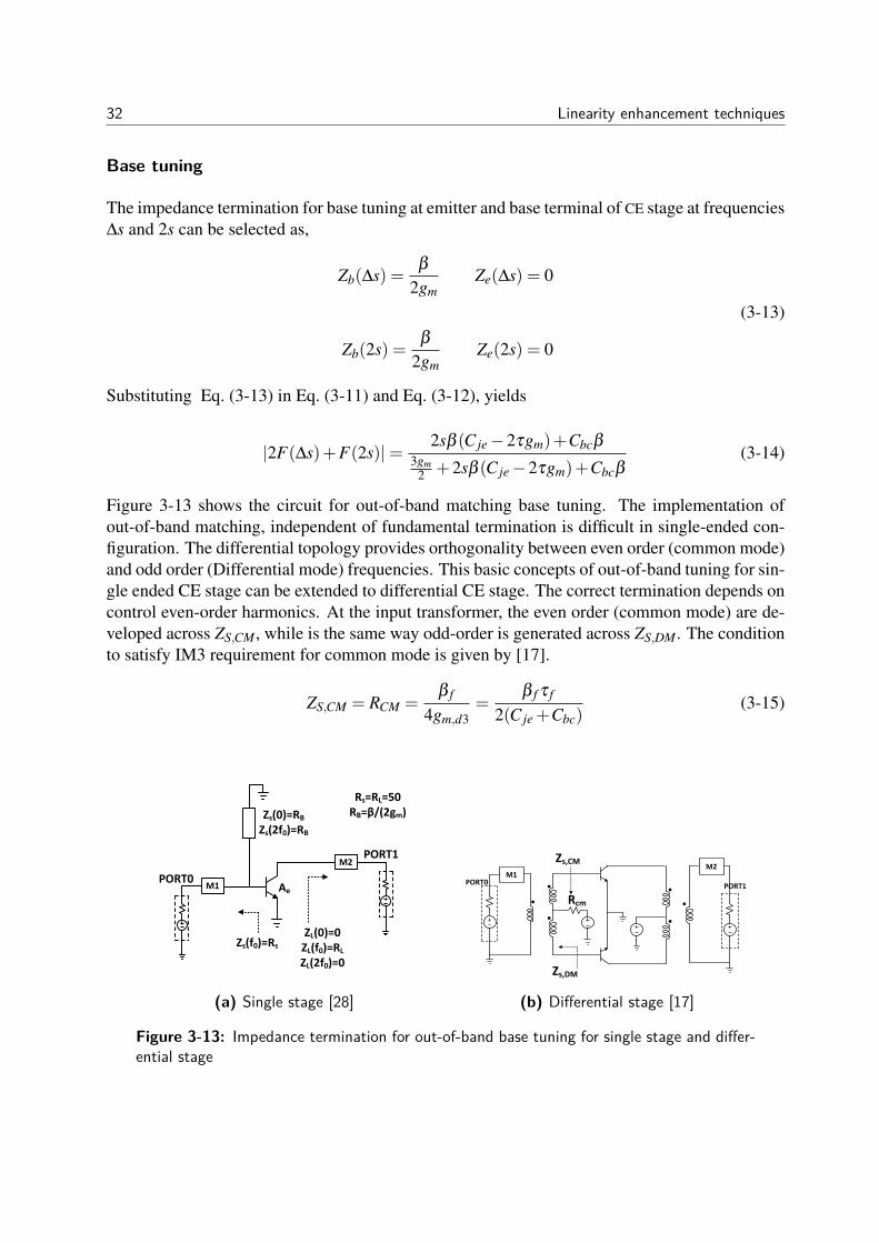
3-13 Impedance termination for out-of-band base tuning for single stage and differ-ential stage . . . . . . . . . . . . . . . . . . . . . . . . . . . . . . . . . . . . 32
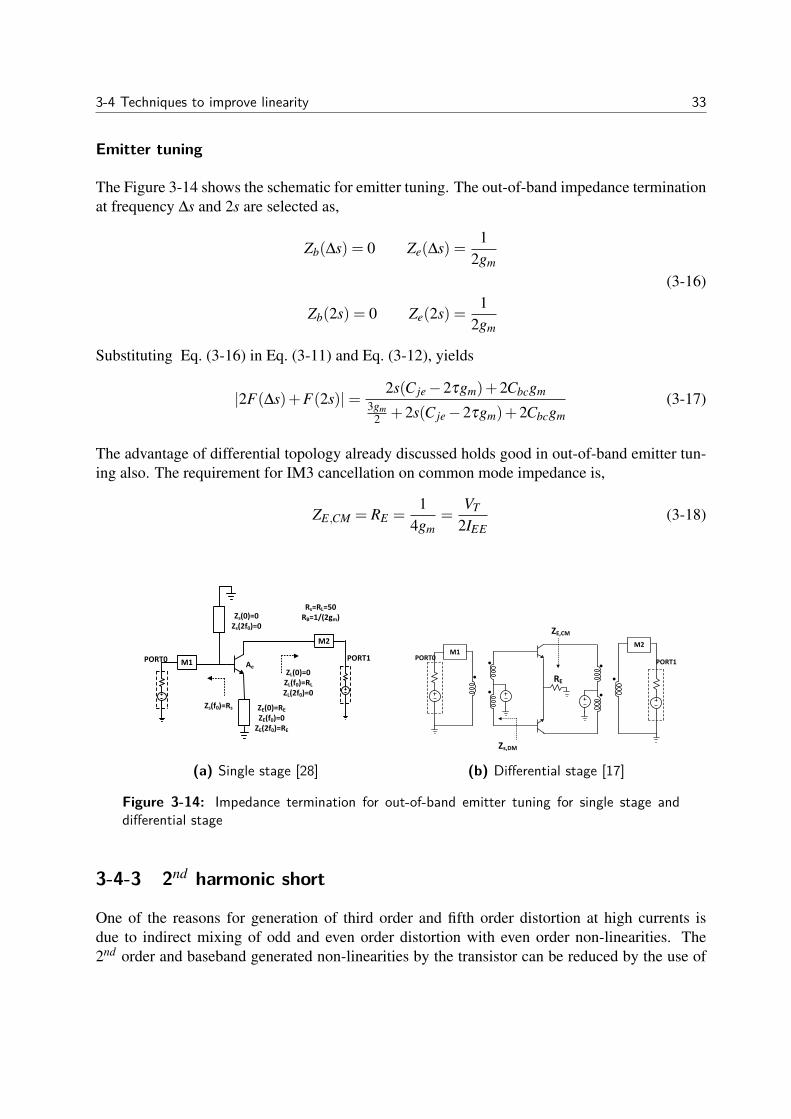
3-14 Impedance termination for out-of-band emitter tuning for single stage and dif-ferential stage . . . . . . . . . . . . . . . . . . . . . . . . . . . . . . . . . . 33
3-15 A 2nd harmonic termination is provided at input and output by series resonator [29] 34
3-16 Even and odd mode operation [29] . . . . . . . . . . . . . . . . . . . . . . . 34
3-17 Resonating out parasitic inductance . . . . . . . . . . . . . . . . . . . . . . . 353-18 Schematic circuits for differential configuration with out-of-band matching for
base tuning . . . . . . . . . . . . . . . . . . . . . . . . . . . . . . . . . . . . 373-19 Contour out-of-band matching for base tuning, for ideal Gummel Poon model . 393-20 Contour out-of-band matching for base tuning, for ideal Gummel Poon model
with C je and τ f . . . . . . . . . . . . . . . . . . . . . . . . . . . . . . . . . 40
3-21 Contour out-of-band matching for base tuning, for ideal Gummel Poon modelwith C je, τ f and C jc . . . . . . . . . . . . . . . . . . . . . . . . . . . . . . . 41
3-22 Schematic circuits for differential configuration with out-of-band matching foremitter tuning . . . . . . . . . . . . . . . . . . . . . . . . . . . . . . . . . . 42
3-23 Contour out-of-band matching for emitter tuning, for ideal Gummel Poon model 443-24 Contour out-of-band matching for emitter tuning, for ideal Gummel Poon model
with C je and τ f . . . . . . . . . . . . . . . . . . . . . . . . . . . . . . . . . 45
3-25 Contour out-of-band matching for emitter tuning, for ideal Gummel Poon modelwith C je, τ f and C jc . . . . . . . . . . . . . . . . . . . . . . . . . . . . . . . 46
4-1 Noise figure @ 2 GHz simulated versus IC, for size:0.3 µm x 1 µm x 1 QUBiC4XiSiGe BNY BJT . . . . . . . . . . . . . . . . . . . . . . . . . . . . . . . . . . 50
4-2 Input stage . . . . . . . . . . . . . . . . . . . . . . . . . . . . . . . . . . . . 514-3 Input matching and noise matching . . . . . . . . . . . . . . . . . . . . . . . 524-4 The variation of S11 and noise figure by C f . . . . . . . . . . . . . . . . . . . 53
4-5 Simulation results of input stage . . . . . . . . . . . . . . . . . . . . . . . . . 534-6 Compression point and linearity performance of the input stage . . . . . . . . 544-7 Common mode test . . . . . . . . . . . . . . . . . . . . . . . . . . . . . . . 554-8 Impedance at 2nd harmonic due to centertap capacitor C2 . . . . . . . . . . . 554-9 Differential Cascode stage . . . . . . . . . . . . . . . . . . . . . . . . . . . . 564-10 Impedance at baseband, fundamental and second harmonic . . . . . . . . . . 574-11 Simulation results of differential cascode stage . . . . . . . . . . . . . . . . . 58
List of Figures ix
4-12 Compression Point and Linearity performance of differential cascode . . . . . . 594-13 Differential CE stage . . . . . . . . . . . . . . . . . . . . . . . . . . . . . . . 604-14 OIP3 variation . . . . . . . . . . . . . . . . . . . . . . . . . . . . . . . . . . 604-15 Impedance at baseband, fundamental and second harmonic . . . . . . . . . . 614-16 Simulation results of differential CE stage . . . . . . . . . . . . . . . . . . . . 624-17 Compression Point and Linearity performance of differential cascode . . . . . . 624-18 LNA with differential Cascode stage . . . . . . . . . . . . . . . . . . . . . . . 634-19 Simulation results of LNA with differential cascode stage . . . . . . . . . . . . 644-20 Compression Point and Linearity performance of LNA with differential cascode 654-21 Monte Carlo simulation of schematic for LNA with differential cascode stage . 654-22 LNA with differential CE stage . . . . . . . . . . . . . . . . . . . . . . . . . 664-23 Simulation results of LNA with differential CE stage . . . . . . . . . . . . . . 674-24 Compression Point and Linearity performance of LNA with differential CE stage 674-25 Monte Carlo simulation of schematic for LNA with differential CE stage . . . . 68
5-1 Final schematic of the overall LNA with differential cascode output stage . . . 725-2 Metal stack . . . . . . . . . . . . . . . . . . . . . . . . . . . . . . . . . . . 725-3 Inductor layout used for various inductor in LNA . . . . . . . . . . . . . . . . 735-4 Balun Layout . . . . . . . . . . . . . . . . . . . . . . . . . . . . . . . . . . . 745-5 Performance of output balun . . . . . . . . . . . . . . . . . . . . . . . . . . 755-6 Guard ring and DTI layer for transistor . . . . . . . . . . . . . . . . . . . . . . 765-7 ESD protection . . . . . . . . . . . . . . . . . . . . . . . . . . . . . . . . . . 775-8 Final layout . . . . . . . . . . . . . . . . . . . . . . . . . . . . . . . . . . . . 775-9 Momentum view of top metal layer . . . . . . . . . . . . . . . . . . . . . . . 785-10 S-parameter . . . . . . . . . . . . . . . . . . . . . . . . . . . . . . . . . . . 795-11 Noise figure at different temperature . . . . . . . . . . . . . . . . . . . . . . 805-12 Stability analysis . . . . . . . . . . . . . . . . . . . . . . . . . . . . . . . . . 805-13 Output compression point for different temperatures . . . . . . . . . . . . . . 815-14 OIP3 for both sidebands . . . . . . . . . . . . . . . . . . . . . . . . . . . . . 815-15 OIP3 vs input tone power @ 1.84 GHz . . . . . . . . . . . . . . . . . . . . . 825-16 Plot of OIP3 due to supply and bias variation @ 1.84 GHz . . . . . . . . . . . 825-17 Histogram of OIP3 . . . . . . . . . . . . . . . . . . . . . . . . . . . . . . . . 83
6-1 Laterally compensated balun [40] . . . . . . . . . . . . . . . . . . . . . . . . 86
6-2 Cross coupled differential stage . . . . . . . . . . . . . . . . . . . . . . . . . 87
A-1 . . . . . . . . . . . . . . . . . . . . . . . . . . . . . . . . . . . . . . . . . . 90
x List of Figures
A-2 OIP3 Vs Input Power . . . . . . . . . . . . . . . . . . . . . . . . . . . . . . 91A-3 Cascode inductive degeneration . . . . . . . . . . . . . . . . . . . . . . . . . 92A-4 OIP3 vs. Le @ 1.84 GHz of the size:0.4 µm x 20.7 µm x 25 QUBiC4Xi SiGe
BNA transistor . . . . . . . . . . . . . . . . . . . . . . . . . . . . . . . . . . 92A-5 OIP3 Vs Input Power . . . . . . . . . . . . . . . . . . . . . . . . . . . . . . 93A-6 An inductive degenerated cascode with feedback . . . . . . . . . . . . . . . . 94A-7 OIP3 Vs Input Power . . . . . . . . . . . . . . . . . . . . . . . . . . . . . . 94
List of Tables
1-1 Comparison table of different fabrication technique [7] . . . . . . . . . . . . . 41-2 Comparison table of different technology w.r.t noise and cost [2] . . . . . . . . 41-3 Commercially available highly linear LNA for base station . . . . . . . . . . . 51-4 Comparison of two different 0.25 µm SiGe BICMOS processes . . . . . . . . . 51-5 Specification for ultra linear LNA . . . . . . . . . . . . . . . . . . . . . . . . . 7
2-1 Specification for two stage . . . . . . . . . . . . . . . . . . . . . . . . . . . . 12
3-1 Parameters used in ideal Gummel Poon model . . . . . . . . . . . . . . . . . 383-2 Parameters used for simplified Gummel Poon model . . . . . . . . . . . . . . 383-3 Parameter used for simplified Gummel Poon model . . . . . . . . . . . . . . . 403-4 Parameters used for simplified Gummel Poon model . . . . . . . . . . . . . . 433-5 Parameters used for simplified Gummel Poon model . . . . . . . . . . . . . . 433-6 Parameters used for simplified Gummel Poon model . . . . . . . . . . . . . . 443-7 Performance for out of band base tuning for all the configurations using Gummel
Poon model . . . . . . . . . . . . . . . . . . . . . . . . . . . . . . . . . . . 473-8 Performance for out of band emitter tuning for all the configurations using
Gummel Poon model . . . . . . . . . . . . . . . . . . . . . . . . . . . . . . . 47
5-1 Dimension and values of inductance used in layout . . . . . . . . . . . . . . . 735-2 Dimension and values of inductance of coils in balun used in layout . . . . . . 745-3 Biasing for different temperatures . . . . . . . . . . . . . . . . . . . . . . . . 795-4 Comparison with state-of-the-art . . . . . . . . . . . . . . . . . . . . . . . . 84
A-1 Design matrix achieved for an inductively degenerated CE stage . . . . . . . . 91A-2 Design Matrix of an inductively degenerated cascode . . . . . . . . . . . . . . 93A-3 Design Matrix of an inductive degenerated cascode with feedback . . . . . . . 95
Master of Science Thesis xi Sanganagouda B Patil

xii List of Tables
Chapter 1
Introduction
In wireless communication industry, cellular communication is a fast growing segment [1]. Thecellular systems are one of the most successful application of the wireless communication. Twomain building blocks of a cellular system are the cellular phone and the base station. Boththese blocks use a same receiver architecture, but differ in their required performance in termsof sensitivity, linearity and power consumption. The base station should provide large area ofcoverage while sharing the same site with many transmitters.
One of the most important functional blocks of a base station receiver is the low noise amplifier.An LNA senses the weak input signal from the antenna and amplifies it. The surrounding filtersreject out-of-band signals, since in practical situations many service providers are accommodatedon the same base station to reduce cost [2]. The basic requirements of an LNA are low noise, highgain, low return loss( IRL), high linearity and output return loss( ORL). Multiple technologiesare available for implementation of an LNA, such as GaAs, SiGe, and etc. An integrated solutionusing one single technology is desired to lower system and test costs. The main focus of thisproject is to implement an ultra-linear LNA for base station using SiGe technology.
1-1 Receiver architecture
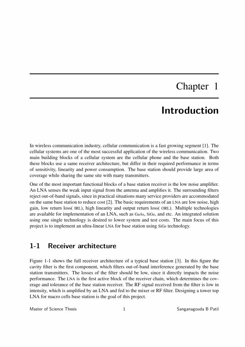
Figure 1-1 shows the full receiver architecture of a typical base station [3]. In this figure thecavity filter is the first component, which filters out-of-band interference generated by the basestation transmitters. The losses of the filter should be low, since it directly impacts the noiseperformance. The LNA is the first active block of the receiver chain, which determines the cov-erage and tolerance of the base station receiver. The RF signal received from the filter is low inintensity, which is amplified by an LNA and fed to the mixer or RF filter. Designing a tower topLNA for macro cells base station is the goal of this project.
Master of Science Thesis 1 Sanganagouda B Patil
2 Introduction
A co-axial cable is used for connecting to the top of the base station to the receiver at the bot-tom(see Figure 1-2). The typical length of this co-axial cable is around 20 m, which resultsapproximately 10 dB losses. To compensate the losses in the coaxial cable an additional groundlevel amplifier is used. The ground level amplifier provides high linearity at moderate noiselevel. The image rejection filter, filters out the noise in the image band before it reaches the downconverting mixer stage in base station receiver. The intermediate filter removes any frequencycomponent other than the desired intermediate frequency IF component. The filter may have lowpass or band pass response depending on the IF frequency.
.
Figure 1-1: Receiver Architecture
1-2 Requirements for base station LNA
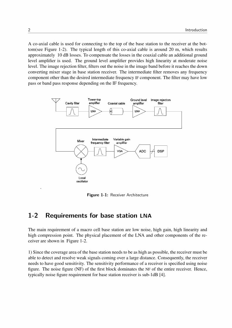
The main requirement of a macro cell base station are low noise, high gain, high linearity andhigh compression point. The physical placement of the LNA and other components of the re-ceiver are shown in Figure 1-2.
1) Since the coverage area of the base station needs to be as high as possible, the receiver must beable to detect and resolve weak signals coming over a large distance. Consequently, the receiverneeds to have good sensitivity. The sensitivity performance of a receiver is specified using noisefigure. The noise figure (NF) of the first block dominates the NF of the entire receiver. Hence,typically noise figure requirement for base station receiver is sub-1dB [4].
1-3 Technologies for LNA 3
2) As shown in Figure 1-2, usually the LNA is kept very close to the antenna for condition-ing the signal before transferring it to a ground unit over a cable [5]. The signal transfer overthe long cable, results in a few dB attenuation. Due to this attenuation in the cable, the gainrequirement of the base station LNA is high.
3) The multiple transceiver present in a typical base station interfere with each other. Conse-quently, the LNA in these receivers should have high linearity to reduce the effect of out-of-bandand in-band interference.
.
Figure 1-2: Base Station
1-3 Technologies for LNA
To achieve all the LNA requirements, different technologies are used. The present generationwireless systems are implemented based on considerations such as low cost, high performance,high integration and short time to market [6]. For high performance application, III-V processtechnologies such as InP and GaAs are available. III-V semiconductor technologies provide HEMTand HBT devices, that use a heterojunction mode of operation [7]. The heterojunction is formedby using different bandgap materials e.g GaAs, InP, SiGe. The device fabrication and propertiesare altered to get good performance at high frequency.

4 Introduction
Table 1-1 compares the performance of HBT and HEMT [7]. HEMT devices provide superiorelectron mobility and velocity compared to HBT. For high-frequency application technologiessuch as GaAs HEMT, GaAs MESFET and SiGe HBT are often used. Table 1-2 compares differenttechnologies with respect to noise figure and cost [2]. From both tables it can seen that byusing GaAs pHEMT the lowest noise figure can be achieved, but the process technology is about200 more times costlier than Silicon.
Table 1-1: Comparison table of different fabrication technique [7]
Merit Parameter HEMT HBT conclusionft M H HBT has highest speedfmax H L HEMT is highest frequencyNoise figure L H HEMT is best for LNAIP3/Pdc M H HBT is best at low frequency
Table 1-2: Comparison table of different technology w.r.t noise and cost [2]
Technology Noise rating Epitaxy cost/mm2
InP pHEMT Very good $10GaAs pHEMT Very good $2GaAs HBT Good $2Si CMOS Fair $0.01
1-4 Motivation and objectives
A low noise figure can be achieved by using optimum design technology and cooling arrange-ments. However, some of these techniques are not feasible for a base station receiver. Forinstance, by using helium cooling a low noise figure can be achieved but its maintenance is tooexpensive to be practically feasible [2]. The other way to achieve low noise is to use more exoticfabrication process and material.
To achieve high linearity the device needs to operate at higher ft . In GaAs pHEMT, the noise islow for a wide range of bias, which helps to achieve low noise and high linearity simultaneously.In SiGe, the noise figure is strongly dependent on the base and collector shot noise. Thus, theminimum noise figure after its sweet spot will increase with current. Hence, this limits a goodtrade-off between the minimum noise figure and linearity. Table 1-3 shows the performancecomparison of different, commercially available LNAs for base station applications.
1-4 Motivation and objectives 5
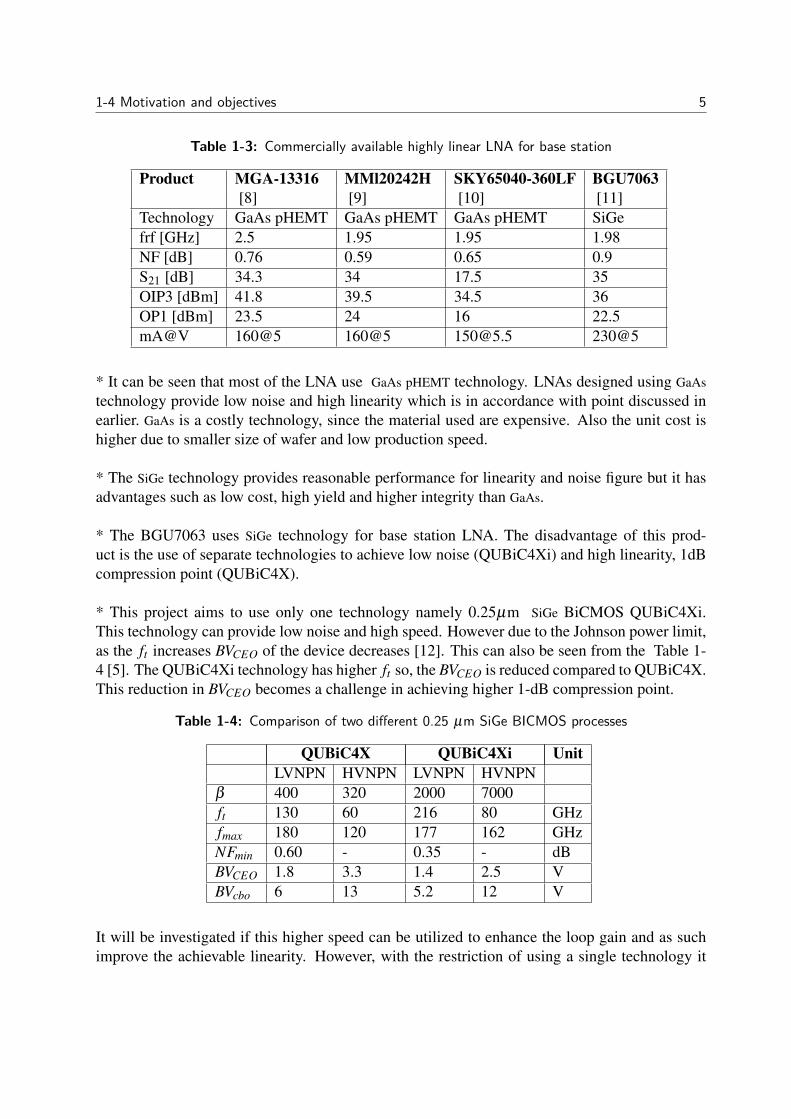
Table 1-3: Commercially available highly linear LNA for base station
Product MGA-13316 MMl20242H SKY65040-360LF BGU7063[8] [9] [10] [11]
Technology GaAs pHEMT GaAs pHEMT GaAs pHEMT SiGefrf [GHz] 2.5 1.95 1.95 1.98NF [dB] 0.76 0.59 0.65 0.9S21 [dB] 34.3 34 17.5 35OIP3 [dBm] 41.8 39.5 34.5 36OP1 [dBm] 23.5 24 16 22.5mA@V 160@5 160@5 [email protected] 230@5
* It can be seen that most of the LNA use GaAs pHEMT technology. LNAs designed using GaAstechnology provide low noise and high linearity which is in accordance with point discussed inearlier. GaAs is a costly technology, since the material used are expensive. Also the unit cost ishigher due to smaller size of wafer and low production speed.
* The SiGe technology provides reasonable performance for linearity and noise figure but it hasadvantages such as low cost, high yield and higher integrity than GaAs.
* The BGU7063 uses SiGe technology for base station LNA. The disadvantage of this prod-uct is the use of separate technologies to achieve low noise (QUBiC4Xi) and high linearity, 1dBcompression point (QUBiC4X).
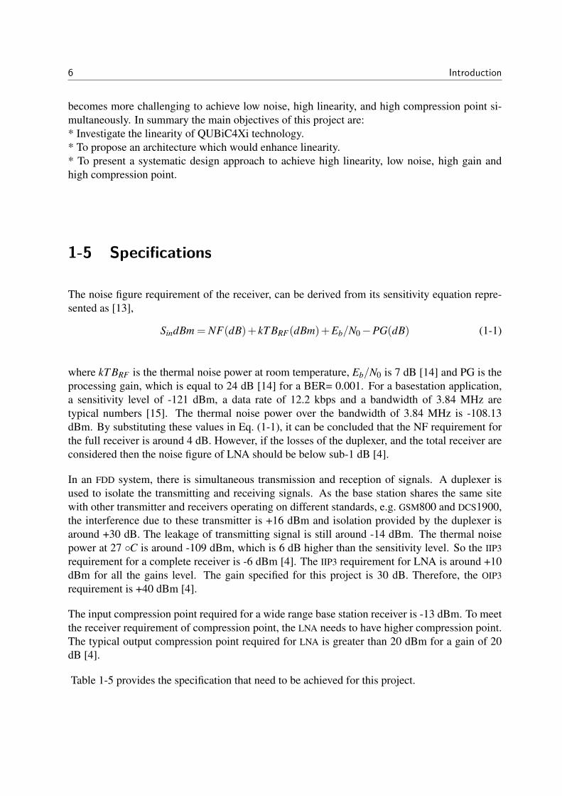
* This project aims to use only one technology namely 0.25µm SiGe BiCMOS QUBiC4Xi.This technology can provide low noise and high speed. However due to the Johnson power limit,as the ft increases BVCEO of the device decreases [12]. This can also be seen from the Table 1-4 [5]. The QUBiC4Xi technology has higher ft so, the BVCEO is reduced compared to QUBiC4X.This reduction in BVCEO becomes a challenge in achieving higher 1-dB compression point.
Table 1-4: Comparison of two different 0.25 µm SiGe BICMOS processes
QUBiC4X QUBiC4Xi UnitLVNPN HVNPN LVNPN HVNPN
β 400 320 2000 7000ft 130 60 216 80 GHzfmax 180 120 177 162 GHzNFmin 0.60 - 0.35 - dBBVCEO 1.8 3.3 1.4 2.5 VBVcbo 6 13 5.2 12 V
It will be investigated if this higher speed can be utilized to enhance the loop gain and as suchimprove the achievable linearity. However, with the restriction of using a single technology it
6 Introduction
becomes more challenging to achieve low noise, high linearity, and high compression point si-multaneously. In summary the main objectives of this project are:* Investigate the linearity of QUBiC4Xi technology.* To propose an architecture which would enhance linearity.* To present a systematic design approach to achieve high linearity, low noise, high gain andhigh compression point.
1-5 Specifications
The noise figure requirement of the receiver, can be derived from its sensitivity equation repre-sented as [13],
SindBm = NF(dB)+ kT BRF(dBm)+Eb/N0−PG(dB) (1-1)
where kT BRF is the thermal noise power at room temperature, Eb/N0 is 7 dB [14] and PG is theprocessing gain, which is equal to 24 dB [14] for a BER= 0.001. For a basestation application,a sensitivity level of -121 dBm, a data rate of 12.2 kbps and a bandwidth of 3.84 MHz aretypical numbers [15]. The thermal noise power over the bandwidth of 3.84 MHz is -108.13dBm. By substituting these values in Eq. (1-1), it can be concluded that the NF requirement forthe full receiver is around 4 dB. However, if the losses of the duplexer, and the total receiver areconsidered then the noise figure of LNA should be below sub-1 dB [4].
In an FDD system, there is simultaneous transmission and reception of signals. A duplexer isused to isolate the transmitting and receiving signals. As the base station shares the same sitewith other transmitter and receivers operating on different standards, e.g. GSM800 and DCS1900,the interference due to these transmitter is +16 dBm and isolation provided by the duplexer isaround +30 dB. The leakage of transmitting signal is still around -14 dBm. The thermal noisepower at 27 C is around -109 dBm, which is 6 dB higher than the sensitivity level. So the IIP3requirement for a complete receiver is -6 dBm [4]. The IIP3 requirement for LNA is around +10dBm for all the gains level. The gain specified for this project is 30 dB. Therefore, the OIP3requirement is +40 dBm [4].
The input compression point required for a wide range base station receiver is -13 dBm. To meetthe receiver requirement of compression point, the LNA needs to have higher compression point.The typical output compression point required for LNA is greater than 20 dBm for a gain of 20dB [4].
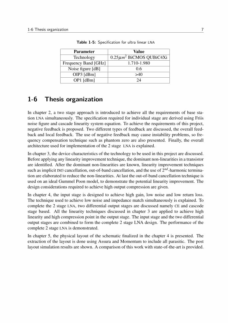
Table 1-5 provides the specification that need to be achieved for this project.
1-6 Thesis organization 7
Table 1-5: Specification for ultra linear LNA
Parameter ValueTechnology 0.25µm2 BiCMOS QUBiC4Xi
Frequency Band [GHz] 1.710-1.980Noise figure [dB] 0.6
OIP3 [dBm] >40OP1 [dBm] 24
1-6 Thesis organization
In chapter 2, a two stage approach is introduced to achieve all the requirements of base sta-tion LNA simultaneously. The specification required for individual stage are derived using Friisnoise figure and cascade linearity system equation. To achieve the requirements of this project,negative feedback is proposed. Two different types of feedback are discussed, the overall feed-back and local feedback. The use of negative feedback may cause instability problems, so fre-quency compensation technique such as phantom zero are also presented. Finally, the overallarchitecture used for implementation of the 2 stage LNA is explained.
In chapter 3, the device characteristics of the technology to be used in this project are discussed.Before applying any linearity improvement technique, the dominant non-linearities in a transistorare identified. After the dominant non-linearities are known, linearity improvement techniquessuch as implicit IM3 cancellation, out-of-band cancellation, and the use of 2nd-harmonic termina-tion are elaborated to reduce the non-linearities. At last the out-of-band cancellation technique isused on an ideal Gummel Poon model, to demonstrate the potential linearity improvement. Thedesign considerations required to achieve high output compression are given.
In chapter 4, the input stage is designed to achieve high gain, low noise and low return loss.The technique used to achieve low noise and impedance match simultaneously is explained. Tocomplete the 2 stage LNA, two differential output stages are discussed namely CE and cascodestage based. All the linearity techniques discussed in chapter 3 are applied to achieve highlinearity and high compression point in the output stage. The input stage and the two differentialoutput stages are combined to form the complete 2 stage LNA design. The performance of thecomplete 2 stage LNA is demonstrated.
In chapter 5, the physical layout of the schematic finalized in the chapter 4 is presented. Theextraction of the layout is done using Assura and Momentum to include all parasitic. The postlayout simulation results are shown. A comparison of this work with state-of-the-art is provided.

8 Introduction
Chapter 2
Low noise amplifier
2-1 Introduction
Basic requirements for wide range base station LNA are low noise, low return loss, high gain,high linearity, and high compression point. The LNA is noise and impedance matched to achievelow noise and low return losses. In order to achieve high gain at high frequency an amplifierchoice needs to be made. The high linearity requirements are satisfied by operating the device athigher ft and using special linearity improvement techniques. In this chapter, the approach usedto achieve linearity and noise simultaneously in SiGe technology is discussed. The related speci-fication required for design approach is derived using Friis and linearity of cascade system equa-tion. To achieve these requirements the negative feedback is used. The frequency compensationtechnique is discussed to improve the stability of the 2 stage system. Finally the implementationof the two stage system along with differential amplifier and transformer are discussed.
In Section 2-2, two stage approach used to to meet the LNA requirement is discussed, followedby in this section the equation and specification related to each stage is explained. In next Sec-tion 2-3, distortion reduction due to negative feedback and stability analysis is discussed. In lastSection 2-4, the two stage design used for implementation is shown.
2-2 Two stage approach
To achieve simultaneously low noise, high gain, high output power and, high linearity using asingle stage is very difficult, due to the conflicting operating conditions of the active device . Onesolution to achieve these requirements is to choose a two stage approach [5]. In the two stageapproach first stage targets low noise and high gain, second stage aims for high linearity and
Master of Science Thesis 9 Sanganagouda B Patil
10 Low noise amplifier
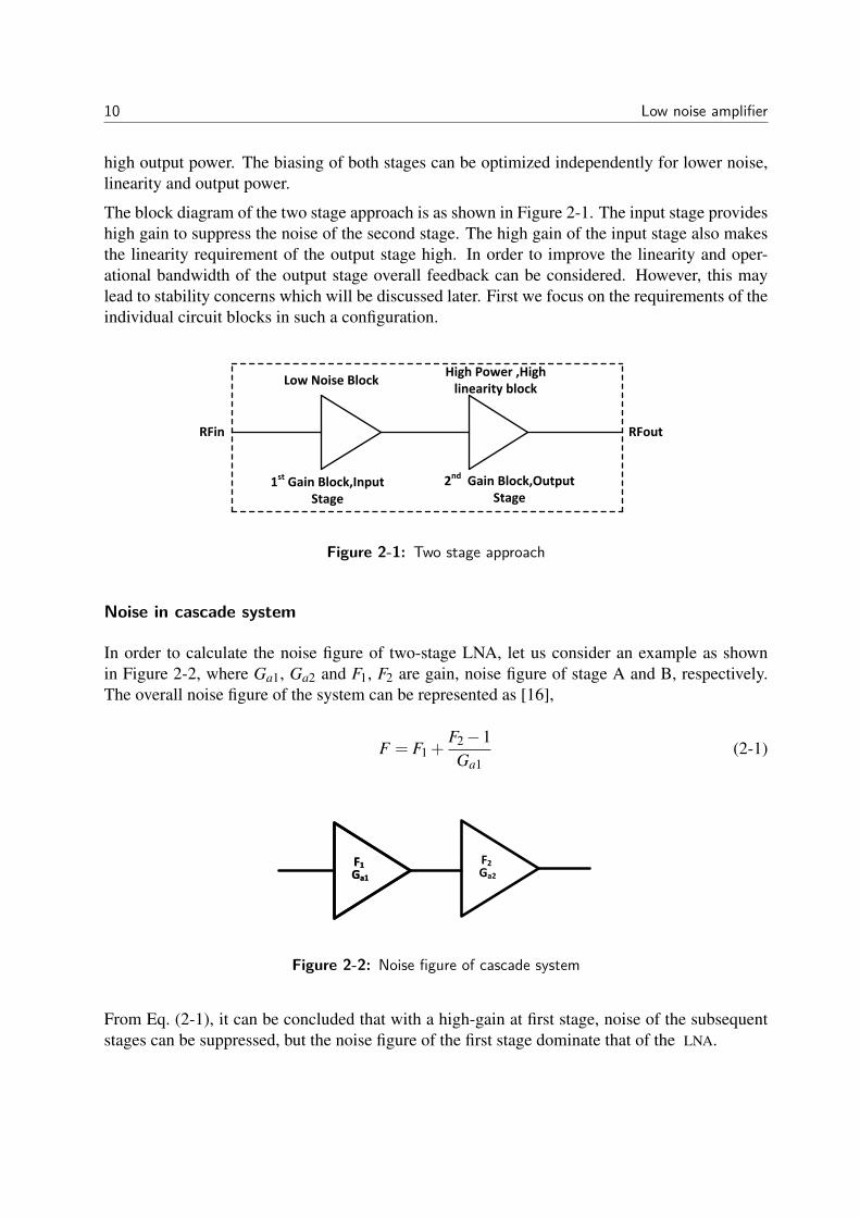
high output power. The biasing of both stages can be optimized independently for lower noise,linearity and output power.
The block diagram of the two stage approach is as shown in Figure 2-1. The input stage provideshigh gain to suppress the noise of the second stage. The high gain of the input stage also makesthe linearity requirement of the output stage high. In order to improve the linearity and oper-ational bandwidth of the output stage overall feedback can be considered. However, this maylead to stability concerns which will be discussed later. First we focus on the requirements of theindividual circuit blocks in such a configuration.
RFin RFout
1st Gain Block,Input Stage
2nd Gain Block,Output Stage
Low Noise BlockHigh Power ,High
linearity block
Figure 2-1: Two stage approach
Noise in cascade system
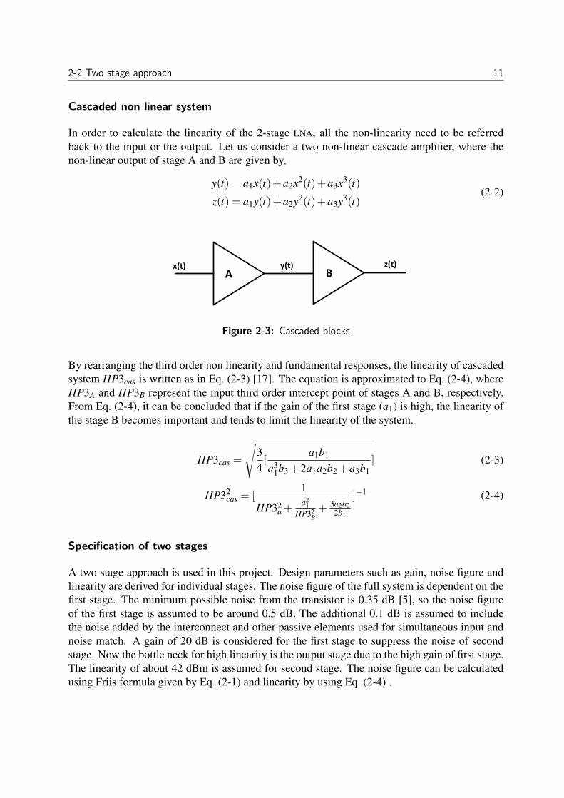
In order to calculate the noise figure of two-stage LNA, let us consider an example as shownin Figure 2-2, where Ga1, Ga2 and F1, F2 are gain, noise figure of stage A and B, respectively.The overall noise figure of the system can be represented as [16],
F = F1 +F2−1Ga1
(2-1)
F1Ga1
F1Ga1
F2Ga2
Figure 2-2: Noise figure of cascade system
From Eq. (2-1), it can be concluded that with a high-gain at first stage, noise of the subsequentstages can be suppressed, but the noise figure of the first stage dominate that of the LNA.
2-2 Two stage approach 11
Cascaded non linear system
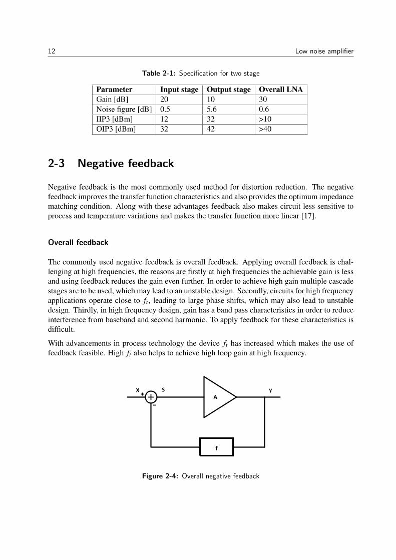
In order to calculate the linearity of the 2-stage LNA, all the non-linearity need to be referredback to the input or the output. Let us consider a two non-linear cascade amplifier, where thenon-linear output of stage A and B are given by,
y(t) = a1x(t)+a2x2(t)+a3x3(t)
z(t) = a1y(t)+a2y2(t)+a3y3(t)(2-2)
A Bx(t) y(t) z(t)
Figure 2-3: Cascaded blocks
By rearranging the third order non linearity and fundamental responses, the linearity of cascadedsystem IIP3cas is written as in Eq. (2-3) [17]. The equation is approximated to Eq. (2-4), whereIIP3A and IIP3B represent the input third order intercept point of stages A and B, respectively.From Eq. (2-4), it can be concluded that if the gain of the first stage (a1) is high, the linearity ofthe stage B becomes important and tends to limit the linearity of the system.
IIP3cas =
√34[
a1b1
a31b3 +2a1a2b2 +a3b1
] (2-3)
IIP32cas = [
1
IIP32a +
a21
IIP32B+ 3a2b2
2b1
]−1 (2-4)
Specification of two stages
A two stage approach is used in this project. Design parameters such as gain, noise figure andlinearity are derived for individual stages. The noise figure of the full system is dependent on thefirst stage. The minimum possible noise from the transistor is 0.35 dB [5], so the noise figureof the first stage is assumed to be around 0.5 dB. The additional 0.1 dB is assumed to includethe noise added by the interconnect and other passive elements used for simultaneous input andnoise match. A gain of 20 dB is considered for the first stage to suppress the noise of secondstage. Now the bottle neck for high linearity is the output stage due to the high gain of first stage.The linearity of about 42 dBm is assumed for second stage. The noise figure can be calculatedusing Friis formula given by Eq. (2-1) and linearity by using Eq. (2-4) .
12 Low noise amplifier
Table 2-1: Specification for two stage
Parameter Input stage Output stage Overall LNAGain [dB] 20 10 30Noise figure [dB] 0.5 5.6 0.6IIP3 [dBm] 12 32 >10OIP3 [dBm] 32 42 >40
2-3 Negative feedback
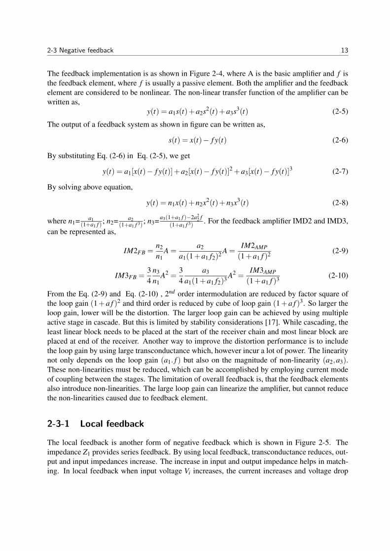
Negative feedback is the most commonly used method for distortion reduction. The negativefeedback improves the transfer function characteristics and also provides the optimum impedancematching condition. Along with these advantages feedback also makes circuit less sensitive toprocess and temperature variations and makes the transfer function more linear [17].
Overall feedback
The commonly used negative feedback is overall feedback. Applying overall feedback is chal-lenging at high frequencies, the reasons are firstly at high frequencies the achievable gain is lessand using feedback reduces the gain even further. In order to achieve high gain multiple cascadestages are to be used, which may lead to an unstable design. Secondly, circuits for high frequencyapplications operate close to ft , leading to large phase shifts, which may also lead to unstabledesign. Thirdly, in high frequency design, gain has a band pass characteristics in order to reduceinterference from baseband and second harmonic. To apply feedback for these characteristics isdifficult.
With advancements in process technology the device ft has increased which makes the use offeedback feasible. High ft also helps to achieve high loop gain at high frequency.
A
f
X S y
Figure 2-4: Overall negative feedback
2-3 Negative feedback 13
The feedback implementation is as shown in Figure 2-4, where A is the basic amplifier and f isthe feedback element, where f is usually a passive element. Both the amplifier and the feedbackelement are considered to be nonlinear. The non-linear transfer function of the amplifier can bewritten as,
y(t) = a1s(t)+a2s2(t)+a3s3(t) (2-5)
The output of a feedback system as shown in figure can be written as,
s(t) = x(t)− f y(t) (2-6)
By substituting Eq. (2-6) in Eq. (2-5), we get
y(t) = a1[x(t)− f y(t)]+a2[x(t)− f y(t)]2 +a3[x(t)− f y(t)]3 (2-7)
By solving above equation,
y(t) = n1x(t)+n2x2(t)+n3x3(t) (2-8)
where n1= a1(1+a1 f ) ; n2= a2
(1+a1 f 3); n3=a3(1+a1 f )−2a2
2 f(1+a1 f 3)
. For the feedback amplifier IMD2 and IMD3,can be represented as,
IM2FB =n2
n1A =
a2
a1(1+a1 f2)2 A =IM2AMP
(1+a1 f )2 (2-9)
IM3FB =34
n3
n1A2 =
34
a3
a1(1+a1 f2)3 A2 =IM3AMP
(1+a1 f )3 (2-10)
From the Eq. (2-9) and Eq. (2-10) , 2nd order intermodulation are reduced by factor square ofthe loop gain (1+a f )2 and third order is reduced by cube of loop gain (1+a f )3. So larger theloop gain, lower will be the distortion. The larger loop gain can be achieved by using multipleactive stage in cascade. But this is limited by stability considerations [17]. While cascading, theleast linear block needs to be placed at the start of the receiver chain and most linear block areplaced at end of the receiver. Another way to improve the distortion performance is to includethe loop gain by using large transconductance which, however incur a lot of power. The linearitynot only depends on the loop gain (a1. f ) but also on the magnitude of non-linearity (a2,a3).These non-linearities must be reduced, which can be accomplished by employing current modeof coupling between the stages. The limitation of overall feedback is, that the feedback elementsalso introduce non-linearities. The large loop gain can linearize the amplifier, but cannot reducethe non-linearities caused due to feedback element.
2-3-1 Local feedback
The local feedback is another form of negative feedback which is shown in Figure 2-5. Theimpedance Z1 provides series feedback. By using local feedback, transconductance reduces, out-put and input impedances increase. The increase in input and output impedance helps in match-ing. In local feedback when input voltage Vi increases, the current increases and voltage drop
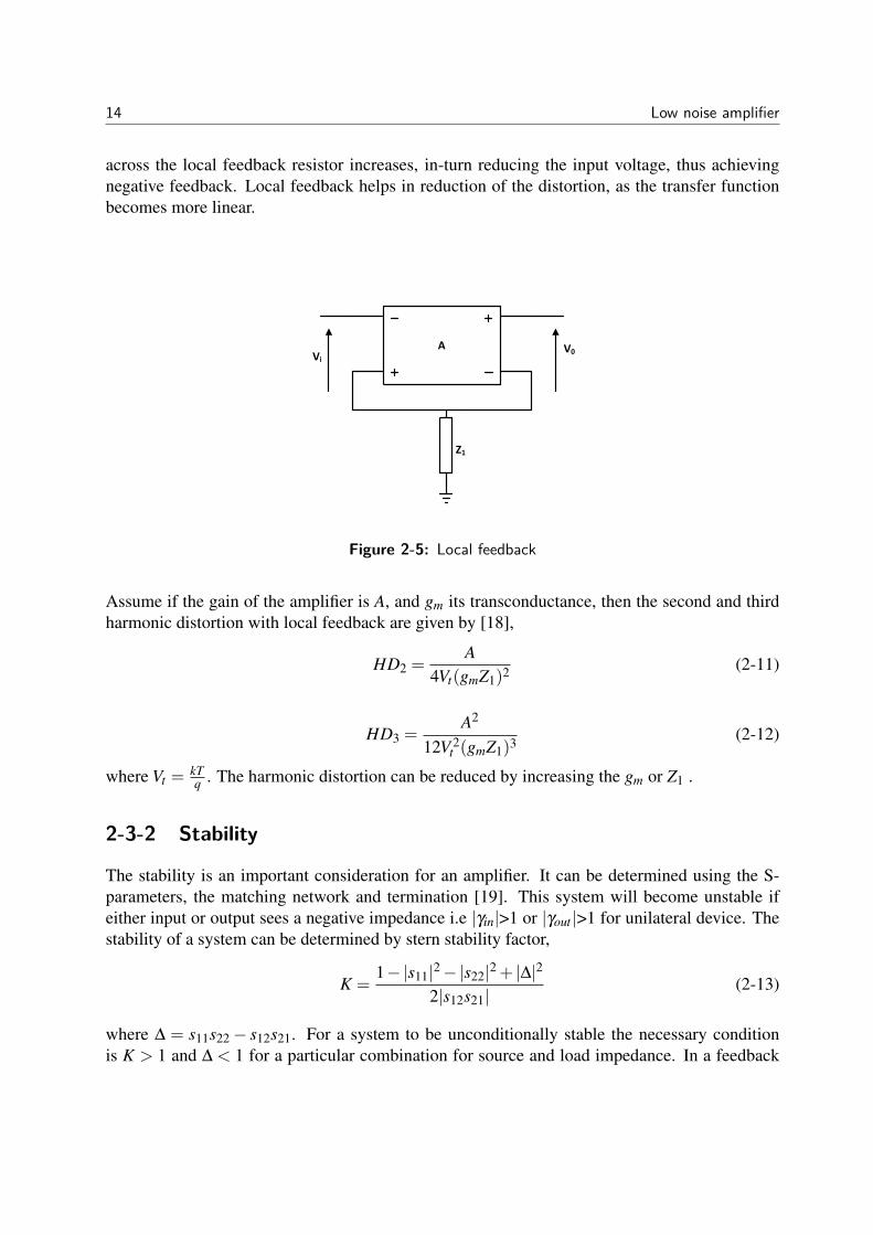
14 Low noise amplifier
across the local feedback resistor increases, in-turn reducing the input voltage, thus achievingnegative feedback. Local feedback helps in reduction of the distortion, as the transfer functionbecomes more linear.
A
Z1
ViV0
Figure 2-5: Local feedback
Assume if the gain of the amplifier is A, and gm its transconductance, then the second and thirdharmonic distortion with local feedback are given by [18],
HD2 =A
4Vt(gmZ1)2 (2-11)
HD3 =A2
12V 2t (gmZ1)3 (2-12)
where Vt =kTq . The harmonic distortion can be reduced by increasing the gm or Z1 .
2-3-2 Stability
The stability is an important consideration for an amplifier. It can be determined using the S-parameters, the matching network and termination [19]. This system will become unstable ifeither input or output sees a negative impedance i.e |γin|>1 or |γout |>1 for unilateral device. Thestability of a system can be determined by stern stability factor,
K =1−|s11|2−|s22|2 + |∆|2
2|s12s21|(2-13)
where ∆ = s11s22− s12s21. For a system to be unconditionally stable the necessary conditionis K > 1 and ∆ < 1 for a particular combination for source and load impedance. In a feedback
2-3 Negative feedback 15
system, for a certain combination of feedback network, source and load impedance, system mightbecome unstable.
Another way of analyzing stability is by pole-zero analysis. An amplifier with a low-pass re-sponse (one dominant pole) will never show instability behavior. If an amplifier has two dom-inant poles, where each pole provides a phase shift of −900, the phase shift will exceed -1800
at high frequencies. And if the loop gain is larger than unity, then the system will oscillate. Inhigh frequency circuit design, frequency response is usually bandpass. If the system is unstable,frequency compensation needs to be applied to make it stable.
Frequency compensation
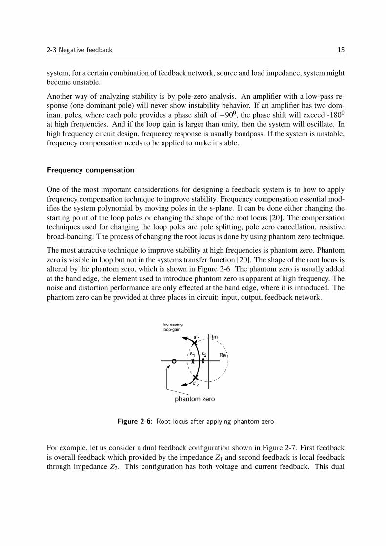
One of the most important considerations for designing a feedback system is to how to applyfrequency compensation technique to improve stability. Frequency compensation essential mod-ifies the system polynomial by moving poles in the s-plane. It can be done either changing thestarting point of the loop poles or changing the shape of the root locus [20]. The compensationtechniques used for changing the loop poles are pole splitting, pole zero cancellation, resistivebroad-banding. The process of changing the root locus is done by using phantom zero technique.
The most attractive technique to improve stability at high frequencies is phantom zero. Phantomzero is visible in loop but not in the systems transfer function [20]. The shape of the root locus isaltered by the phantom zero, which is shown in Figure 2-6. The phantom zero is usually addedat the band edge, the element used to introduce phantom zero is apparent at high frequency. Thenoise and distortion performance are only effected at the band edge, where it is introduced. Thephantom zero can be provided at three places in circuit: input, output, feedback network.
Figure 2-6: Root locus after applying phantom zero
For example, let us consider a dual feedback configuration shown in Figure 2-7. First feedbackis overall feedback which provided by the impedance Z1 and second feedback is local feedbackthrough impedance Z2. This configuration has both voltage and current feedback. This dual
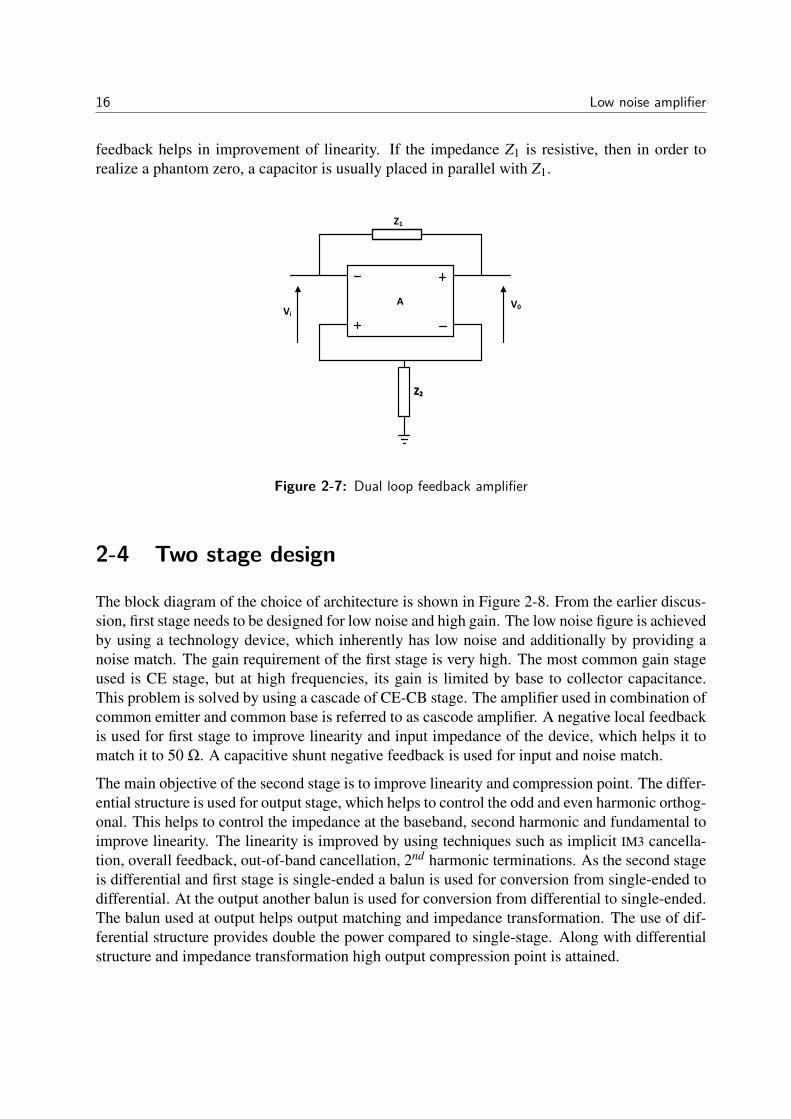
16 Low noise amplifier
feedback helps in improvement of linearity. If the impedance Z1 is resistive, then in order torealize a phantom zero, a capacitor is usually placed in parallel with Z1.
A
Z2Z2
Z1
ViV0
Figure 2-7: Dual loop feedback amplifier
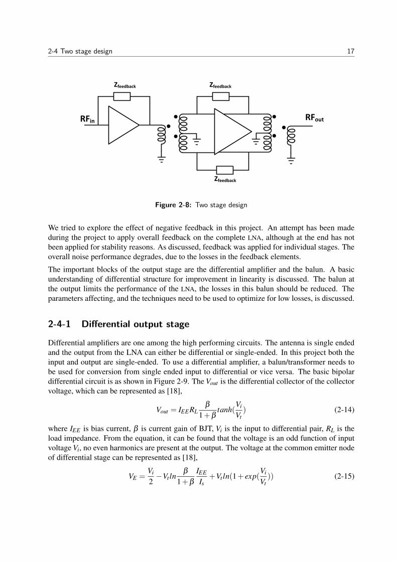
2-4 Two stage design
The block diagram of the choice of architecture is shown in Figure 2-8. From the earlier discus-sion, first stage needs to be designed for low noise and high gain. The low noise figure is achievedby using a technology device, which inherently has low noise and additionally by providing anoise match. The gain requirement of the first stage is very high. The most common gain stageused is CE stage, but at high frequencies, its gain is limited by base to collector capacitance.This problem is solved by using a cascade of CE-CB stage. The amplifier used in combination ofcommon emitter and common base is referred to as cascode amplifier. A negative local feedbackis used for first stage to improve linearity and input impedance of the device, which helps it tomatch it to 50 Ω. A capacitive shunt negative feedback is used for input and noise match.
The main objective of the second stage is to improve linearity and compression point. The differ-ential structure is used for output stage, which helps to control the odd and even harmonic orthog-onal. This helps to control the impedance at the baseband, second harmonic and fundamental toimprove linearity. The linearity is improved by using techniques such as implicit IM3 cancella-tion, overall feedback, out-of-band cancellation, 2nd harmonic terminations. As the second stageis differential and first stage is single-ended a balun is used for conversion from single-ended todifferential. At the output another balun is used for conversion from differential to single-ended.The balun used at output helps output matching and impedance transformation. The use of dif-ferential structure provides double the power compared to single-stage. Along with differentialstructure and impedance transformation high output compression point is attained.
2-4 Two stage design 17
RFin RFout
Zfeedback Zfeedback
Zfeedback
Figure 2-8: Two stage design
We tried to explore the effect of negative feedback in this project. An attempt has been madeduring the project to apply overall feedback on the complete LNA, although at the end has notbeen applied for stability reasons. As discussed, feedback was applied for individual stages. Theoverall noise performance degrades, due to the losses in the feedback elements.
The important blocks of the output stage are the differential amplifier and the balun. A basicunderstanding of differential structure for improvement in linearity is discussed. The balun atthe output limits the performance of the LNA, the losses in this balun should be reduced. Theparameters affecting, and the techniques need to be used to optimize for low losses, is discussed.
2-4-1 Differential output stage
Differential amplifiers are one among the high performing circuits. The antenna is single endedand the output from the LNA can either be differential or single-ended. In this project both theinput and output are single-ended. To use a differential amplifier, a balun/transformer needs tobe used for conversion from single ended input to differential or vice versa. The basic bipolardifferential circuit is as shown in Figure 2-9. The Vout is the differential collector of the collectorvoltage, which can be represented as [18],
Vout = IEERLβ
1+βtanh(
Vi
Vt) (2-14)
where IEE is bias current, β is current gain of BJT, Vi is the input to differential pair, RL is theload impedance. From the equation, it can be found that the voltage is an odd function of inputvoltage Vi, no even harmonics are present at the output. The voltage at the common emitter nodeof differential stage can be represented as [18],
VE =Vi
2−Vt ln
β
1+β
IEE
Is+Vt ln(1+ exp(
Vi
Vt)) (2-15)
18 Low noise amplifier
The voltage VE is an even function of input voltage. If both the Vi2 and −Vi
2 are interchanged, thenalso VE voltage changes exactly in identical manner. Thus, it can be said that there are no oddharmonics present at this node. The tail node is AC ground, when the circuit is linearized. Thishelps to reduce the non-linearities caused by even harmonics. The overall distortion performanceof system can be improved.
.
RLRL
Vout
IEE
VDD
Vi/2 -Vi/2VE
Figure 2-9: Basic Common emitter Differential pair
In a differential pair, equal and opposite AC voltage and currents flows in two differentialbranches. If the layout is symmetrical then the two branches have equal coupling with the refer-ence system. The introduced AC current in the reference system from one branch is counteractedby the equal and opposite from the other branch.
In layout, at high frequency metal interconnect connecting to ground plane has a finite impedance.The noise generated by the signal returning from ground, across the finite impedance to ground isreferred to as ground bounce. Due to ground bounce both the differential branch will be effectedequally. But due to the counteract nature of the differential branches, the common mode signalwill get canceled.
2-4-2 Transformer
A transformer transfers power from the primary to the secondary coil using mutual coupling. Thepower transfer should happen with low loss. The impedance is transformed between the coilsdepending on the turns ratio. If an alternating current ip flows in primary it induces a currentin secondary is. In the ideal transformer the current and voltage transformation between thewinding is expressed in terms of turns ratio n as [21],
n =vs
vp=
ip
is=
√LP
LS(2-16)
2-4 Two stage design 19
where (vp, vs), (ip, is) are voltages and currents in primary and secondary coils respectively. Lp,Ls are the self inductance of primary and secondary coils, respectively. The energy with whichpower is transferred between the coils depends on magnetic coupling which is given by Eq. (2-17), where M is mutual inductance.
km =M√LPLS
(2-17)
The quality of the transformer is evaluated by the maximum available gain. It can be expressedin terms of quality factor and mutual coupling of the primary and secondary coils. The maxi-mum gain is limited by mutual resistive coupling with silicon substrate and also quality factorof the primary and secondary coils [22]. For maximum power transfer the efficiency should behigh. The efficiency can be defined as the ratio of power delivered to load to input power. Themaximum gain is expressed in terms of S-parameters as [22],
Gmax = |s21
s12|(k−
√k2−1) (2-18)
k =1−|s11|2−|s22|2 + |∆|2
2|s12s21|(2-19)
∆ = s11s22− s12s21 (2-20)
The alternative expression for max gain is,
Gmax = 1+2(x−√
x2 + x) (2-21)
x =Re(z11)Re(z22)− [Re(z12)]
2
[Re(z12)]2 +[Re(z12)]2(2-22)
where zi j(i,j=1,2) are impedance matrix of transformer. The mutual reactive (kIm) and mutualresistive (kRe) coupling factor is represented by [22],
kIm =
√[Im(z12]2
Im(z11)Im(Z22)
kRe =
√[Re(z12]2
Re(z11)Re(Z22)
(2-23)
The kIm is mutual reactive coupling factor, equal to mutual magnetic coupling factor at lowfrequency but deviates at high frequency due to capacitance between the primary and secondary.The kRe is the mutual resistive coupling factor at high frequency and zero at low frequency dueto the coupling between the inductor is dominant. The x in the Eq. (2-22) can also be written interms of kRe, kIm, QP = jωLP
RP,QS =
jωLSRS
as [22],
x =1− k2
Re
k2ImQPQS + k2
Re(2-24)
20 Low noise amplifier
In order to obtain higher Gmax, the x should be lowered by increasing Qp, Qs, kRe and kIm. Thelosses in transformer can be reduced by maximizing for mutual coupling and optimizing forcoupling factor. The use of differential pair and transformer, helps to achieve two requirement,one is high linearity and other is high compression point.
2-5 Conclusion
In this chapter, the two stage approach which is used to achieve all the requirements simultane-ously for wide range LNA is discussed. The specification requirements for individual stages suchas gain, noise figure, and linearity were derived. Negative feedback is used for multiple purposessuch as for linearity improvements, noise and impedance match. The use of negative feedbackmay lead to stability issues, so the frequency compensation technique used to improve stabilityis discussed. The final architecture used for implementation of 2 stage LNA and its componentare explained.
Chapter 3
Linearity enhancement techniques
3-1 Introduction
In a two stage approach, the output stage has to provide high linearity and high compressionpoint. In this chapter, the techniques used to improve linearity and compression point are dis-cussed. Initially, the device characteristics such as DC characteristics, small signal model, andfigure of merit are shown. The dominant non-linearities present in the bipolar transistor are iden-tified and the techniques to mitigate them are discussed. These linearity improvement techniquesare applied on an “ideal” Gummel Poon transistor representation to better understand their indi-vidual impact on the overall linearity. (Note that the Gummel-Poon model allows a much morestraightforward simplification of the transistor than the more accurate Mextram model descrip-tion). Another important requirement of this project is the output 1 dB compression point , whichis limited by the technology. A circuit technique to improve the 1 dB compression point is alsodiscussed. For all the simulation in this chapter Cadence Spectre and ADS were used.
In Section 3-2 the device characteristics are discussed. In next Section 3-3, the reference circuitand the dominant non-linearities in a transistor are presented. The technique to improve linearityare discussed in Section 3-4. The limitation of technology and technique to improve compressionpoint is discussed in Section 3-5. In last Section 3-6, the out-of-band linearization technique isapplied on the ideal Gummel Poon model to see the impact of each parasitic on linearity.
3-2 Device characteristics
The technology used for this project is 0.25 µm SiGe BiCMOS QUBiC4Xi. In this section, theDC characteristics, small signal model, and figure of merit used to characterize the transistor arediscussed.
Master of Science Thesis 21 Sanganagouda B Patil
22 Linearity enhancement techniques
3-2-1 DC characteristics
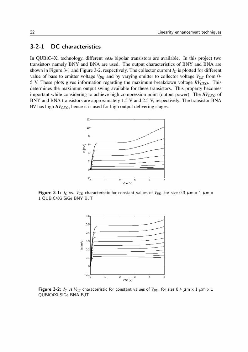
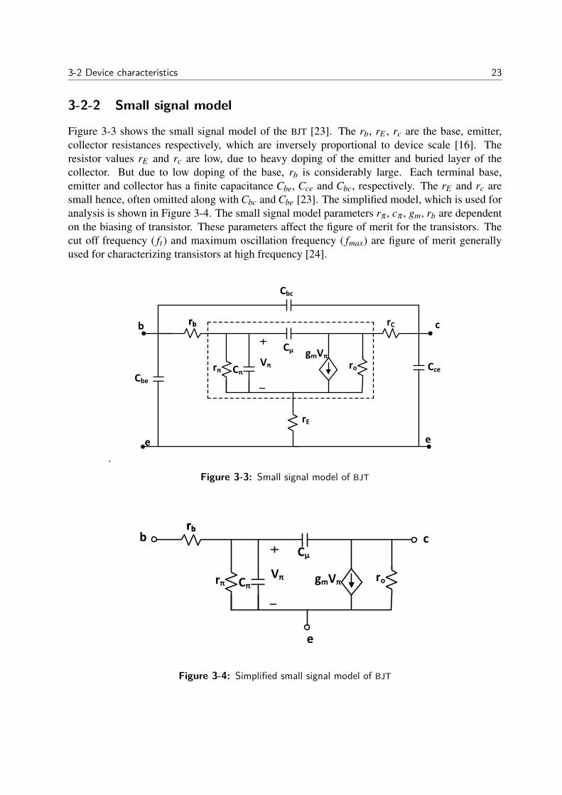
In QUBiC4Xi technology, different SiGe bipolar transistors are available. In this project twotransistors namely BNY and BNA are used. The output characteristics of BNY and BNA areshown in Figure 3-1 and Figure 3-2, respectively. The collector current IC is plotted for differentvalue of base to emitter voltage VBE and by varying emitter to collector voltage VCE from 0-5 V. These plots gives information regarding the maximum breakdown voltage BVCEO. Thisdetermines the maximum output swing available for these transistors. This property becomesimportant while considering to achieve high compression point (output power). The BVCEO ofBNY and BNA transistors are approximately 1.5 V and 2.5 V, respectively. The transistor BNAHV has high BVCEO, hence it is used for high output delivering stages.
0 1 2 3 4 5−2
0
2
4
6
8
10
12
Vce [V]
Ic [m
A]
Figure 3-1: IC vs. VCE characteristic for constant values of VBE , for size 0.3 µm x 1 µm x1 QUBiC4Xi SiGe BNY BJT
0 1 2 3 4 5−0.1
0
0.1
0.2
0.3
0.4
0.5
0.6
Vce [V]
Ic [m
A]
Figure 3-2: IC vs VCE characteristic for constant values of VBE , for size 0.4 µm x 1 µm x 1QUBiC4Xi SiGe BNA BJT
3-2 Device characteristics 23
3-2-2 Small signal model
Figure 3-3 shows the small signal model of the BJT [23]. The rb, rE , rc are the base, emitter,collector resistances respectively, which are inversely proportional to device scale [16]. Theresistor values rE and rc are low, due to heavy doping of the emitter and buried layer of thecollector. But due to low doping of the base, rb is considerably large. Each terminal base,emitter and collector has a finite capacitance Cbe, Cce and Cbc, respectively. The rE and rc aresmall hence, often omitted along with Cbc and Cbe [23]. The simplified model, which is used foranalysis is shown in Figure 3-4. The small signal model parameters rπ , cπ , gm, rb are dependenton the biasing of transistor. These parameters affect the figure of merit for the transistors. Thecut off frequency ( ft) and maximum oscillation frequency ( fmax) are figure of merit generallyused for characterizing transistors at high frequency [24].
.
Cbc
rb
rE
rC
Cbe
Cce
rb
rπ Cπ
gmVπ ro Vπ
b c
e
Cµ
e
Figure 3-3: Small signal model of BJT
rbrb
rπ Cπ gmVπ ro Vπ
Cµ b c
e
Figure 3-4: Simplified small signal model of BJT
24 Linearity enhancement techniques
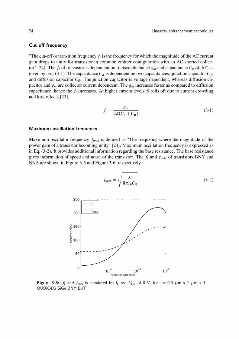
Cut off frequency
"The cut-off or transition frequency ft is the frequency for which the magnitude of the AC currentgain drops to unity for transistor in common emitter configuration with an AC-shorted collec-tor" [24]. The ft of transistor is dependent on transconductance gm and capacitance Cπ of BJT asgiven by Eq. (3-1). The capacitance Cπ is dependent on two capacitances: junction capacitor C jeand diffusion capacitor Cd . The junction capacitor is voltage dependent, whereas diffusion ca-pacitor and gm are collector current dependent. The gm increases faster as compared to diffusioncapacitance, hence the ft increases. At higher current levels ft rolls off due to current crowdingand kirk effects [23].
ft =gm
2π(Cπ +Cµ)(3-1)
Maximum oscillation frequency
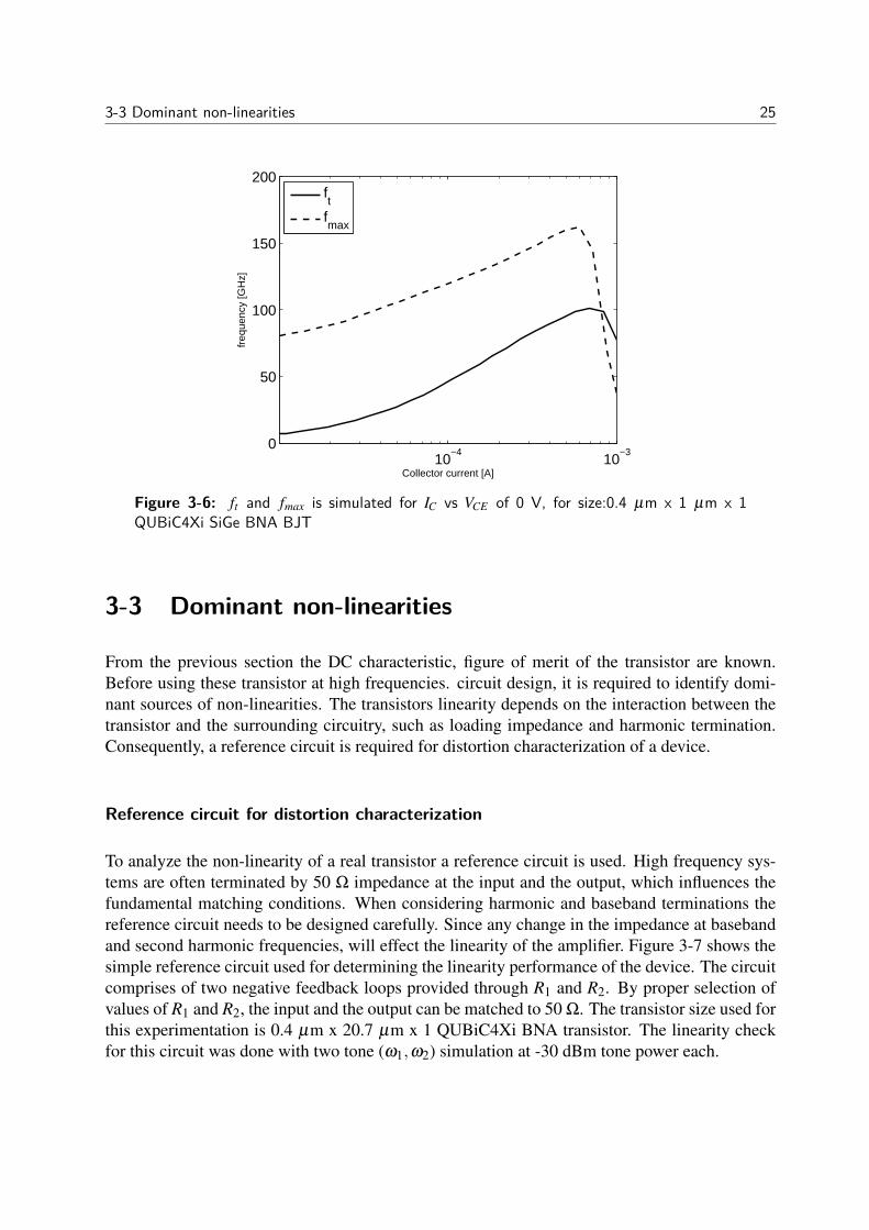
Maximum oscillator frequency fmax is defined as "The frequency where the magnitude of thepower gain of a transistor becoming unity" [24]. Maximum oscillation frequency is expressed asin Eq. (3-2). It provides additional information regarding the base resistance. The base resistancegives information of speed and noise of the transistor. The ft and fmax of transistors BNY andBNA are shown in Figure 3-5 and Figure 3-6, respectively.
fmax =
√ft
8πrbCπ
(3-2)
10−4
10−3
10−2
0
50
100
150
200
250
Collector current [A]
freq
uenc
y [G
Hz]
ft
fmax
Figure 3-5: ft and fmax is simulated for IC vs. VCE of 0 V, for size:0.3 µm x 1 µm x 1QUBiC4Xi SiGe BNY BJT
3-3 Dominant non-linearities 25
10−4
10−3
0
50
100
150
200
Collector current [A]
freq
uenc
y [G
Hz]
ft
fmax
Figure 3-6: ft and fmax is simulated for IC vs VCE of 0 V, for size:0.4 µm x 1 µm x 1QUBiC4Xi SiGe BNA BJT
3-3 Dominant non-linearities
From the previous section the DC characteristic, figure of merit of the transistor are known.Before using these transistor at high frequencies. circuit design, it is required to identify domi-nant sources of non-linearities. The transistors linearity depends on the interaction between thetransistor and the surrounding circuitry, such as loading impedance and harmonic termination.Consequently, a reference circuit is required for distortion characterization of a device.
Reference circuit for distortion characterization
To analyze the non-linearity of a real transistor a reference circuit is used. High frequency sys-tems are often terminated by 50 Ω impedance at the input and the output, which influences thefundamental matching conditions. When considering harmonic and baseband terminations thereference circuit needs to be designed carefully. Since any change in the impedance at basebandand second harmonic frequencies, will effect the linearity of the amplifier. Figure 3-7 shows thesimple reference circuit used for determining the linearity performance of the device. The circuitcomprises of two negative feedback loops provided through R1 and R2. By proper selection ofvalues of R1 and R2, the input and the output can be matched to 50 Ω. The transistor size used forthis experimentation is 0.4 µm x 20.7 µm x 1 QUBiC4Xi BNA transistor. The linearity checkfor this circuit was done with two tone (ω1,ω2) simulation at -30 dBm tone power each.
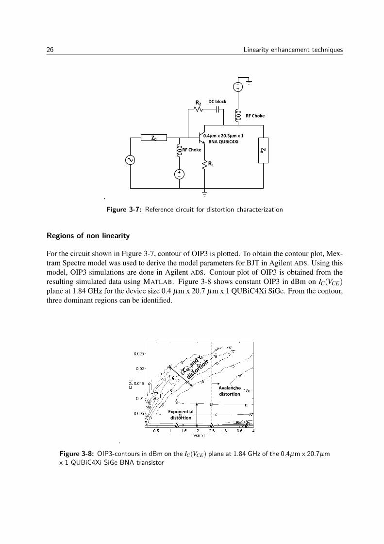
26 Linearity enhancement techniques
.
Z0
Z0
RF Choke
RF Choke
DC block
R1
R2
0.4µm x 20.3µm x 1 BNA QUBiC4Xi
Figure 3-7: Reference circuit for distortion characterization
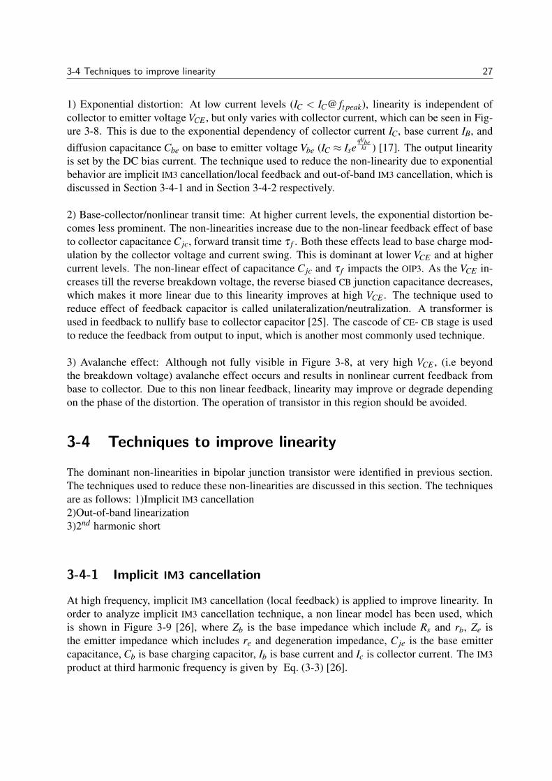
Regions of non linearity
For the circuit shown in Figure 3-7, contour of OIP3 is plotted. To obtain the contour plot, Mex-tram Spectre model was used to derive the model parameters for BJT in Agilent ADS. Using thismodel, OIP3 simulations are done in Agilent ADS. Contour plot of OIP3 is obtained from theresulting simulated data using MATLAB. Figure 3-8 shows constant OIP3 in dBm on IC(VCE)plane at 1.84 GHz for the device size 0.4 µm x 20.7 µm x 1 QUBiC4Xi SiGe. From the contour,three dominant regions can be identified.
.
Avalanche distortion
C bc and τ f
distorti
on
Exponential distortion
Figure 3-8: OIP3-contours in dBm on the IC(VCE) plane at 1.84 GHz of the 0.4µm x 20.7µmx 1 QUBiC4Xi SiGe BNA transistor
3-4 Techniques to improve linearity 27
1) Exponential distortion: At low current levels (IC < IC@ ft peak), linearity is independent ofcollector to emitter voltage VCE , but only varies with collector current, which can be seen in Fig-ure 3-8. This is due to the exponential dependency of collector current IC, base current IB, anddiffusion capacitance Cbe on base to emitter voltage Vbe (IC ≈ Ise
qVbekt ) [17]. The output linearity
is set by the DC bias current. The technique used to reduce the non-linearity due to exponentialbehavior are implicit IM3 cancellation/local feedback and out-of-band IM3 cancellation, which isdiscussed in Section 3-4-1 and in Section 3-4-2 respectively.
2) Base-collector/nonlinear transit time: At higher current levels, the exponential distortion be-comes less prominent. The non-linearities increase due to the non-linear feedback effect of baseto collector capacitance C jc, forward transit time τ f . Both these effects lead to base charge mod-ulation by the collector voltage and current swing. This is dominant at lower VCE and at highercurrent levels. The non-linear effect of capacitance C jc and τ f impacts the OIP3. As the VCE in-creases till the reverse breakdown voltage, the reverse biased CB junction capacitance decreases,which makes it more linear due to this linearity improves at high VCE . The technique used toreduce effect of feedback capacitor is called unilateralization/neutralization. A transformer isused in feedback to nullify base to collector capacitor [25]. The cascode of CE- CB stage is usedto reduce the feedback from output to input, which is another most commonly used technique.
3) Avalanche effect: Although not fully visible in Figure 3-8, at very high VCE , (i.e beyondthe breakdown voltage) avalanche effect occurs and results in nonlinear current feedback frombase to collector. Due to this non linear feedback, linearity may improve or degrade dependingon the phase of the distortion. The operation of transistor in this region should be avoided.
3-4 Techniques to improve linearity
The dominant non-linearities in bipolar junction transistor were identified in previous section.The techniques used to reduce these non-linearities are discussed in this section. The techniquesare as follows: 1)Implicit IM3 cancellation2)Out-of-band linearization3)2nd harmonic short
3-4-1 Implicit IM3 cancellation
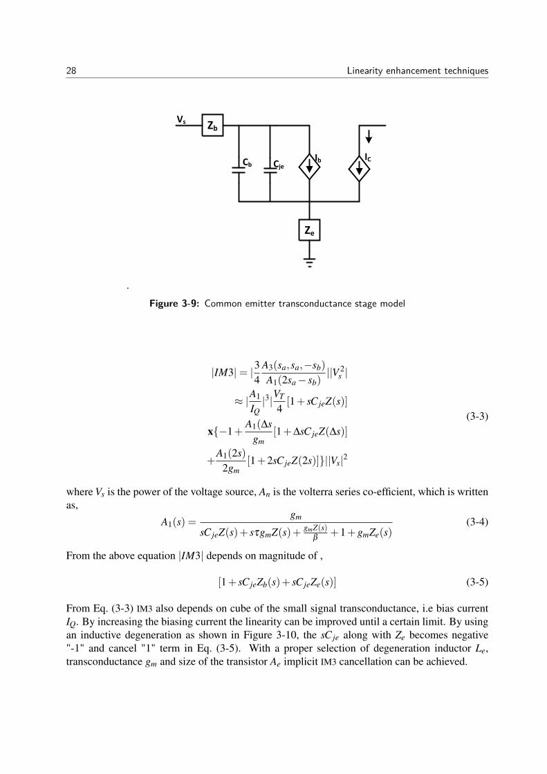
At high frequency, implicit IM3 cancellation (local feedback) is applied to improve linearity. Inorder to analyze implicit IM3 cancellation technique, a non linear model has been used, whichis shown in Figure 3-9 [26], where Zb is the base impedance which include Rs and rb, Ze isthe emitter impedance which includes re and degeneration impedance, C je is the base emittercapacitance, Cb is base charging capacitor, Ib is base current and Ic is collector current. The IM3product at third harmonic frequency is given by Eq. (3-3) [26].
28 Linearity enhancement techniques
.
Zb
ICIb
Ze
CjeCb
Vs
Figure 3-9: Common emitter transconductance stage model
|IM3|= |34
A3(sa,sa,−sb)
A1(2sa− sb)||V 2
s |
≈ |A1
IQ|3|VT
4[1+ sC jeZ(s)]
x−1+A1(∆s
gm[1+∆sC jeZ(∆s)]
+A1(2s)
2gm[1+2sC jeZ(2s)]||Vs|2
(3-3)
where Vs is the power of the voltage source, An is the volterra series co-efficient, which is writtenas,
A1(s) =gm
sC jeZ(s)+ sτgmZ(s)+ gmZ(s)β
+1+gmZe(s)(3-4)
From the above equation |IM3| depends on magnitude of ,
[1+ sC jeZb(s)+ sC jeZe(s)] (3-5)
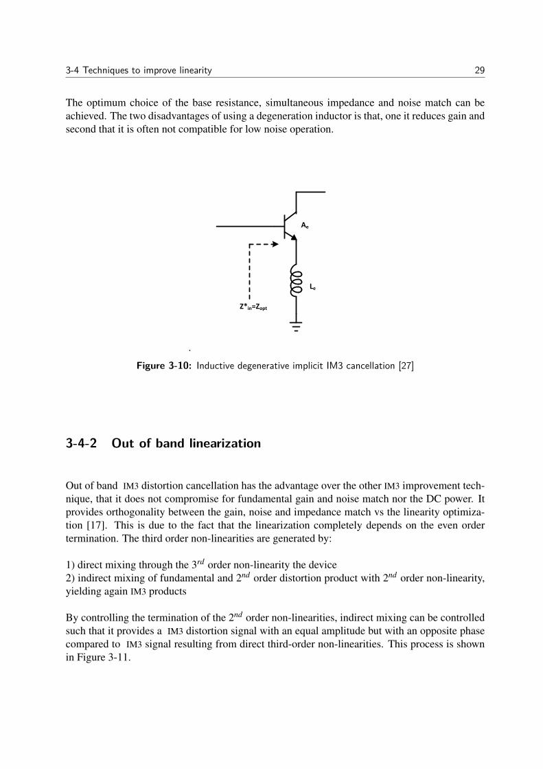
From Eq. (3-3) IM3 also depends on cube of the small signal transconductance, i.e bias currentIQ. By increasing the biasing current the linearity can be improved until a certain limit. By usingan inductive degeneration as shown in Figure 3-10, the sC je along with Ze becomes negative"-1" and cancel "1" term in Eq. (3-5). With a proper selection of degeneration inductor Le,transconductance gm and size of the transistor Ae implicit IM3 cancellation can be achieved.
3-4 Techniques to improve linearity 29
The optimum choice of the base resistance, simultaneous impedance and noise match can beachieved. The two disadvantages of using a degeneration inductor is that, one it reduces gain andsecond that it is often not compatible for low noise operation.
.
Z*in=Zopt
Le
Ae
Figure 3-10: Inductive degenerative implicit IM3 cancellation [27]
3-4-2 Out of band linearization
Out of band IM3 distortion cancellation has the advantage over the other IM3 improvement tech-nique, that it does not compromise for fundamental gain and noise match nor the DC power. Itprovides orthogonality between the gain, noise and impedance match vs the linearity optimiza-tion [17]. This is due to the fact that the linearization completely depends on the even ordertermination. The third order non-linearities are generated by:
1) direct mixing through the 3rd order non-linearity the device2) indirect mixing of fundamental and 2nd order distortion product with 2nd order non-linearity,yielding again IM3 products
By controlling the termination of the 2nd order non-linearities, indirect mixing can be controlledsuch that it provides a IM3 distortion signal with an equal amplitude but with an opposite phasecompared to IM3 signal resulting from direct third-order non-linearities. This process is shownin Figure 3-11.
30 Linearity enhancement techniques
.
Figure 3-11: Out of band IM3 cancellation [17]
The large signal circuit used for investigation of linearity improvement for CE stage using out-of-band linearization is shown in Figure 3-12 [17]. The exponential distortion is considered tobe the dominant source of the non-linearity. The effect of base to collector capacitance is alsoconsidered for derivation, since the distortion cancellation depends on all the circuit parasitics.The IIP3 for CE stage can be expressed as [17],
IIP3 =1
6R|H1b(s)|3|D(s)||ε(∆s,2s)|(3-6)
.
Figure 3-12: Large signal model for CE stage [17]
For Eq. (3-6), three different terms can be identified. Firstly, H1b(s) is transfer function of the
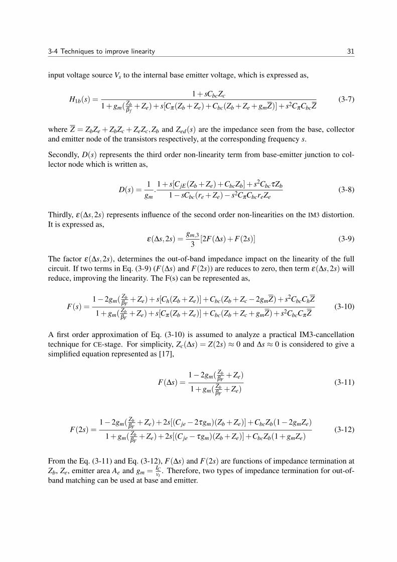
3-4 Techniques to improve linearity 31
input voltage source Vs to the internal base emitter voltage, which is expressed as,
H1b(s) =1+ sCbcZc
1+gm(Zbβ f
+Ze)+ s[Cπ(Zb +Ze)+Cbc(Zb +Ze +gmZ)]+ s2CπCbcZ(3-7)
where Z = ZbZe +ZbZc +ZeZc,Zb and Zed(s) are the impedance seen from the base, collectorand emitter node of the transistors respectively, at the corresponding frequency s.
Secondly, D(s) represents the third order non-linearity term from base-emitter junction to col-lector node which is written as,
D(s) =1
gm.1+ s[C jE(Zb +Ze)+CbcZb]+ s2CbcτZb
1− sCbc(re +Ze)− s2CπCbcreZe(3-8)
Thirdly, ε(∆s,2s) represents influence of the second order non-linearities on the IM3 distortion.It is expressed as,
ε(∆s,2s) =gm,3
3[2F(∆s)+F(2s)] (3-9)
The factor ε(∆s,2s), determines the out-of-band impedance impact on the linearity of the fullcircuit. If two terms in Eq. (3-9) (F(∆s) and F(2s)) are reduces to zero, then term ε(∆s,2s) willreduce, improving the linearity. The F(s) can be represented as,
F(s) =1−2gm(
ZbβF
+Ze)+ s[Ch(Zb +Ze)]+Cbc(Zb +Zc−2gmZ)+ s2CbcChZ
1+gm(ZbβF
+Ze)+ s[Cπ(Zb +Ze)]+Cbc(Zb +Zc +gmZ)+ s2CbcCπZ(3-10)
A first order approximation of Eq. (3-10) is assumed to analyze a practical IM3-cancellationtechnique for CE-stage. For simplicity, Zc(∆s) = Z(2s) ≈ 0 and ∆s ≈ 0 is considered to give asimplified equation represented as [17],
F(∆s) =1−2gm(
ZbβF
+Ze)
1+gm(ZbβF
+Ze)(3-11)
F(2s) =1−2gm(
ZbβF
+Ze)+2s[(C je−2τgm)(Zb +Ze)]+CbcZb(1−2gmZe)
1+gm(ZbβF
+Ze)+2s[(C je− τgm)(Zb +Ze)]+CbcZb(1+gmZe)(3-12)
From the Eq. (3-11) and Eq. (3-12), F(∆s) and F(2s) are functions of impedance termination atZb, Ze, emitter area Ae and gm = IC
vt. Therefore, two types of impedance termination for out-of-
band matching can be used at base and emitter.
32 Linearity enhancement techniques
Base tuning
The impedance termination for base tuning at emitter and base terminal of CE stage at frequencies∆s and 2s can be selected as,
Zb(∆s) =β
2gmZe(∆s) = 0
Zb(2s) =β
2gmZe(2s) = 0
(3-13)
Substituting Eq. (3-13) in Eq. (3-11) and Eq. (3-12), yields
|2F(∆s)+F(2s)|=2sβ (C je−2τgm)+Cbcβ
3gm2 +2sβ (C je−2τgm)+Cbcβ
(3-14)
Figure 3-13 shows the circuit for out-of-band matching base tuning. The implementation ofout-of-band matching, independent of fundamental termination is difficult in single-ended con-figuration. The differential topology provides orthogonality between even order (common mode)and odd order (Differential mode) frequencies. This basic concepts of out-of-band tuning for sin-gle ended CE stage can be extended to differential CE stage. The correct termination depends oncontrol even-order harmonics. At the input transformer, the even order (common mode) are de-veloped across ZS,CM, while is the same way odd-order is generated across ZS,DM. The conditionto satisfy IM3 requirement for common mode is given by [17].
ZS,CM = RCM =β f
4gm,d3=
β f τ f
2(C je +Cbc)(3-15)
Rs=RL=50RB=β/(2gm)Zs(0)=RB
Zs(2f0)=RB
ZL(0)=0ZL(f0)=RL
ZL(2f0)=0
Ae
Zs(f0)=Rs
M1
M2
PORT0
PORT1
(a) Single stage [28]
PORT1PORT0
Rcm
M1M2
Zs,CM
Zs,DM
(b) Differential stage [17]
Figure 3-13: Impedance termination for out-of-band base tuning for single stage and differ-ential stage
3-4 Techniques to improve linearity 33
Emitter tuning
The Figure 3-14 shows the schematic for emitter tuning. The out-of-band impedance terminationat frequency ∆s and 2s are selected as,
Zb(∆s) = 0 Ze(∆s) =1
2gm
Zb(2s) = 0 Ze(2s) =1
2gm
(3-16)
Substituting Eq. (3-16) in Eq. (3-11) and Eq. (3-12), yields
|2F(∆s)+F(2s)|=2s(C je−2τgm)+2Cbcgm
3gm2 +2s(C je−2τgm)+2Cbcgm
(3-17)
The advantage of differential topology already discussed holds good in out-of-band emitter tun-ing also. The requirement for IM3 cancellation on common mode impedance is,
ZE,CM = RE =1
4gm=
VT
2IEE(3-18)
Rs=RL=50RB=1/(2gm)Zs(0)=0
Zs(2f0)=0
Ae
ZE(0)=RE
ZE(f0)=0ZE(2f0)=RE
Zs(f0)=Rs
M1ZL(0)=0ZL(f0)=RL
ZL(2f0)=0
M2
PORT0 PORT1
(a) Single stage [28]
PORT1PORT0
RE
M1M2
ZE,CM
Zs,DM
(b) Differential stage [17]
Figure 3-14: Impedance termination for out-of-band emitter tuning for single stage anddifferential stage
3-4-3 2nd harmonic short
One of the reasons for generation of third order and fifth order distortion at high currents isdue to indirect mixing of odd and even order distortion with even order non-linearities. The2nd order and baseband generated non-linearities by the transistor can be reduced by the use of
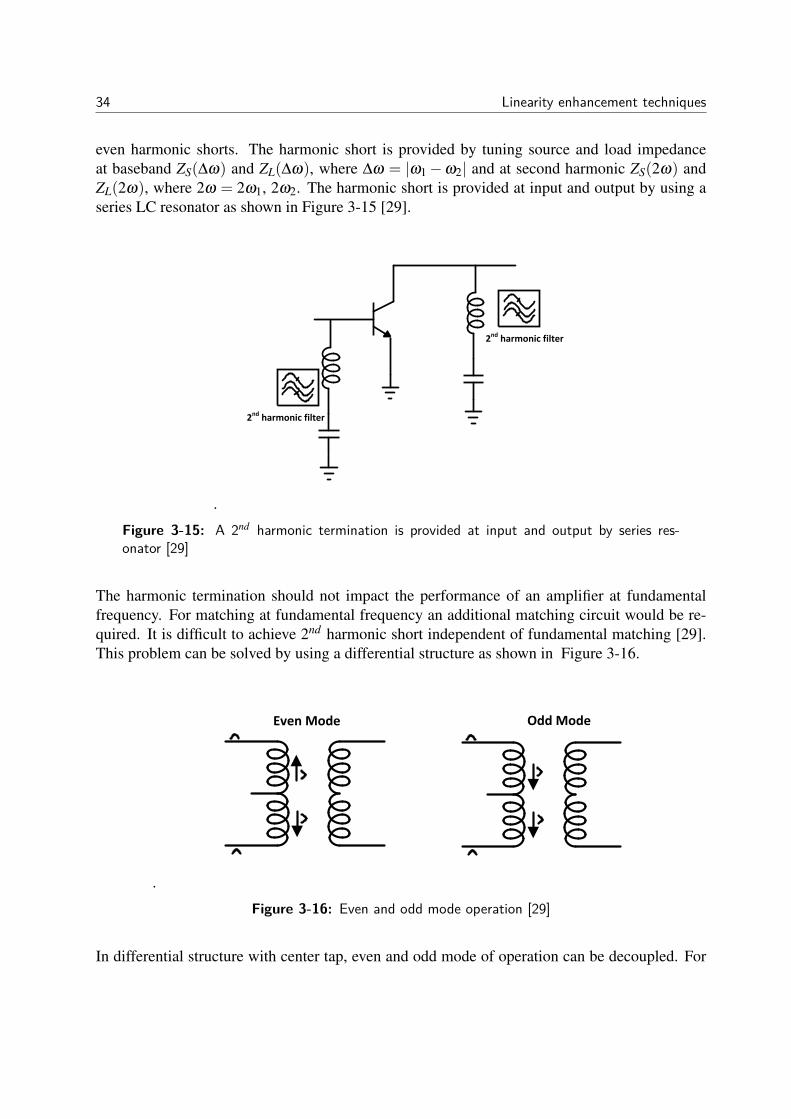
34 Linearity enhancement techniques
even harmonic shorts. The harmonic short is provided by tuning source and load impedanceat baseband ZS(∆ω) and ZL(∆ω), where ∆ω = |ω1−ω2| and at second harmonic ZS(2ω) andZL(2ω), where 2ω = 2ω1, 2ω2. The harmonic short is provided at input and output by using aseries LC resonator as shown in Figure 3-15 [29].
.
2nd harmonic filter
2nd harmonic filter
Figure 3-15: A 2nd harmonic termination is provided at input and output by series res-onator [29]
The harmonic termination should not impact the performance of an amplifier at fundamentalfrequency. For matching at fundamental frequency an additional matching circuit would be re-quired. It is difficult to achieve 2nd harmonic short independent of fundamental matching [29].This problem can be solved by using a differential structure as shown in Figure 3-16.
.
Even Mode Odd Mode
Figure 3-16: Even and odd mode operation [29]
In differential structure with center tap, even and odd mode of operation can be decoupled. For
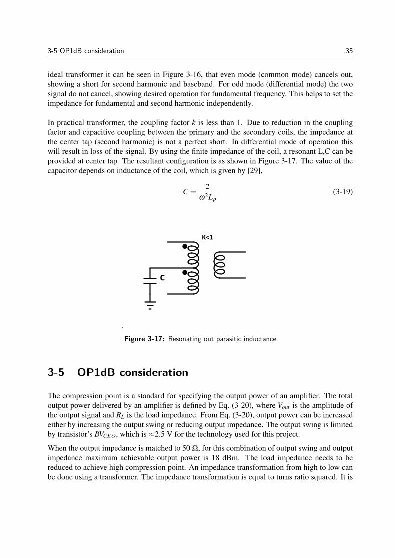
3-5 OP1dB consideration 35
ideal transformer it can be seen in Figure 3-16, that even mode (common mode) cancels out,showing a short for second harmonic and baseband. For odd mode (differential mode) the twosignal do not cancel, showing desired operation for fundamental frequency. This helps to set theimpedance for fundamental and second harmonic independently.
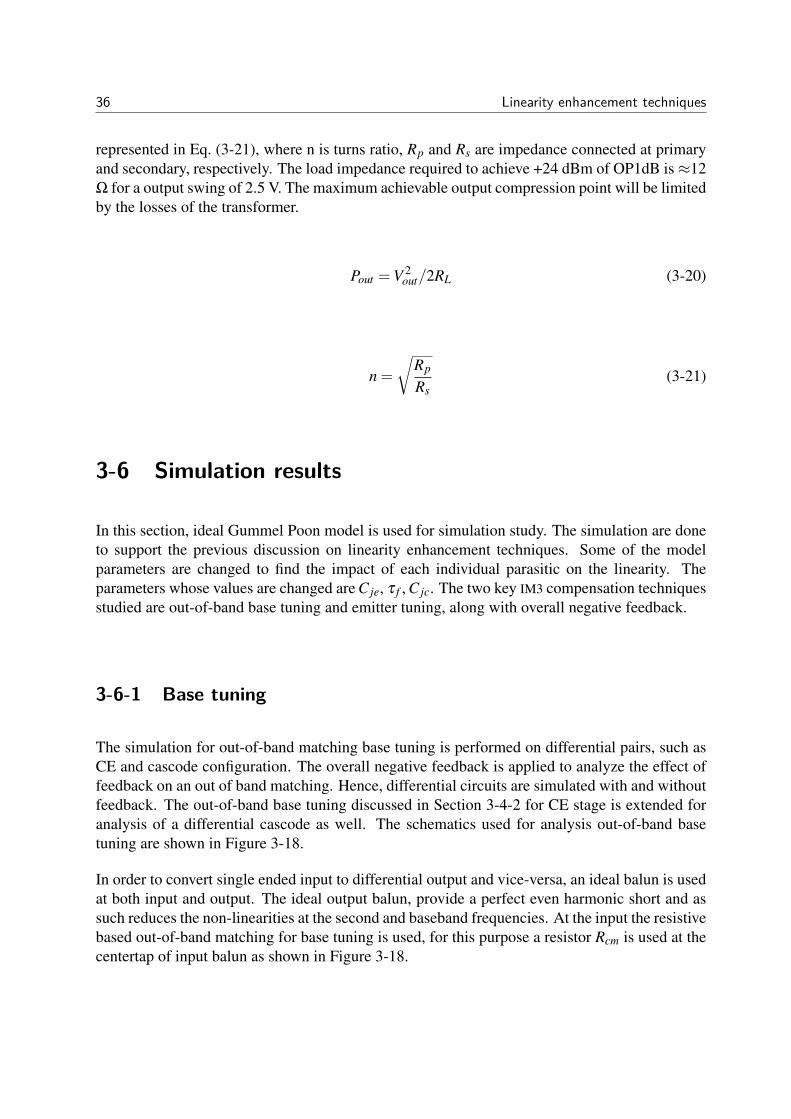
In practical transformer, the coupling factor k is less than 1. Due to reduction in the couplingfactor and capacitive coupling between the primary and the secondary coils, the impedance atthe center tap (second harmonic) is not a perfect short. In differential mode of operation thiswill result in loss of the signal. By using the finite impedance of the coil, a resonant L,C can beprovided at center tap. The resultant configuration is as shown in Figure 3-17. The value of thecapacitor depends on inductance of the coil, which is given by [29],
C =2
ω2Lp(3-19)
.
K<1
C
Figure 3-17: Resonating out parasitic inductance
3-5 OP1dB consideration
The compression point is a standard for specifying the output power of an amplifier. The totaloutput power delivered by an amplifier is defined by Eq. (3-20), where Vout is the amplitude ofthe output signal and RL is the load impedance. From Eq. (3-20), output power can be increasedeither by increasing the output swing or reducing output impedance. The output swing is limitedby transistor’s BVCEO, which is ≈2.5 V for the technology used for this project.
When the output impedance is matched to 50 Ω, for this combination of output swing and outputimpedance maximum achievable output power is 18 dBm. The load impedance needs to bereduced to achieve high compression point. An impedance transformation from high to low canbe done using a transformer. The impedance transformation is equal to turns ratio squared. It is
36 Linearity enhancement techniques
represented in Eq. (3-21), where n is turns ratio, Rp and Rs are impedance connected at primaryand secondary, respectively. The load impedance required to achieve +24 dBm of OP1dB is≈12Ω for a output swing of 2.5 V. The maximum achievable output compression point will be limitedby the losses of the transformer.
Pout =V 2out/2RL (3-20)
n =
√Rp
Rs(3-21)
3-6 Simulation results
In this section, ideal Gummel Poon model is used for simulation study. The simulation are doneto support the previous discussion on linearity enhancement techniques. Some of the modelparameters are changed to find the impact of each individual parasitic on the linearity. Theparameters whose values are changed are C je, τ f , C jc. The two key IM3 compensation techniquesstudied are out-of-band base tuning and emitter tuning, along with overall negative feedback.
3-6-1 Base tuning
The simulation for out-of-band matching base tuning is performed on differential pairs, such asCE and cascode configuration. The overall negative feedback is applied to analyze the effect offeedback on an out of band matching. Hence, differential circuits are simulated with and withoutfeedback. The out-of-band base tuning discussed in Section 3-4-2 for CE stage is extended foranalysis of a differential cascode as well. The schematics used for analysis out-of-band basetuning are shown in Figure 3-18.
In order to convert single ended input to differential output and vice-versa, an ideal balun is usedat both input and output. The ideal output balun, provide a perfect even harmonic short and assuch reduces the non-linearities at the second and baseband frequencies. At the input the resistivebased out-of-band matching for base tuning is used, for this purpose a resistor Rcm is used at thecentertap of input balun as shown in Figure 3-18.
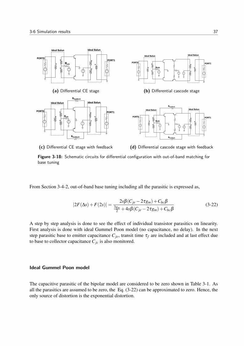
3-6 Simulation results 37
PORT1PORT0
Ideal Balun Ideal Balun
Rcm
(a) Differential CE stage
r
r
PORT1PORT0
Ideal Balun Ideal Balun
Rcm
(b) Differential cascode stage
PORT1PORT0
Ideal Balun Ideal Balun
RCM
Rfeedback
Rfeedback
(c) Differential CE stage with feedback
r
r
PORT1PORT0
Ideal Balun Ideal Balun
Rfeedback
Rfeedback
Rcm
(d) Differential cascode stage with feedback
Figure 3-18: Schematic circuits for differential configuration with out-of-band matching forbase tuning
From Section 3-4-2, out-of-band base tuning including all the parasitic is expressed as,
|2F(∆s)+F(2s)|=2sβ (C je−2τgm)+Cbcβ
3gm2 +4sβ (C je−2τgm)+Cbcβ
(3-22)
A step by step analysis is done to see the effect of individual transistor parasitics on linearity.First analysis is done with ideal Gummel Poon model (no capacitance, no delay). In the nextstep parasitic base to emitter capacitance C je, transit time τ f are included and at last effect dueto base to collector capacitance C jc is also monitored.
Ideal Gummel Poon model
The capacitive parasitic of the bipolar model are considered to be zero shown in Table 3-1. Asall the parasitics are assumed to be zero, the Eq. (3-22) can be approximated to zero. Hence, theonly source of distortion is the exponential distortion.
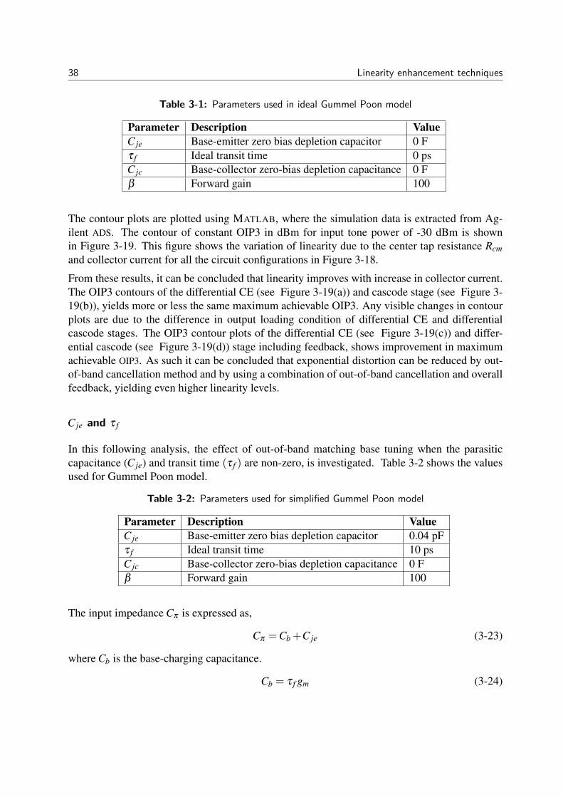
38 Linearity enhancement techniques
Table 3-1: Parameters used in ideal Gummel Poon model
Parameter Description ValueC je Base-emitter zero bias depletion capacitor 0 Fτ f Ideal transit time 0 psC jc Base-collector zero-bias depletion capacitance 0 Fβ Forward gain 100
The contour plots are plotted using MATLAB, where the simulation data is extracted from Ag-ilent ADS. The contour of constant OIP3 in dBm for input tone power of -30 dBm is shownin Figure 3-19. This figure shows the variation of linearity due to the center tap resistance Rcmand collector current for all the circuit configurations in Figure 3-18.
From these results, it can be concluded that linearity improves with increase in collector current.The OIP3 contours of the differential CE (see Figure 3-19(a)) and cascode stage (see Figure 3-19(b)), yields more or less the same maximum achievable OIP3. Any visible changes in contourplots are due to the difference in output loading condition of differential CE and differentialcascode stages. The OIP3 contour plots of the differential CE (see Figure 3-19(c)) and differ-ential cascode (see Figure 3-19(d)) stage including feedback, shows improvement in maximumachievable OIP3. As such it can be concluded that exponential distortion can be reduced by out-of-band cancellation method and by using a combination of out-of-band cancellation and overallfeedback, yielding even higher linearity levels.
C je and τ f
In this following analysis, the effect of out-of-band matching base tuning when the parasiticcapacitance (C je) and transit time (τ f ) are non-zero, is investigated. Table 3-2 shows the valuesused for Gummel Poon model.
Table 3-2: Parameters used for simplified Gummel Poon model
Parameter Description ValueC je Base-emitter zero bias depletion capacitor 0.04 pFτ f Ideal transit time 10 psC jc Base-collector zero-bias depletion capacitance 0 Fβ Forward gain 100
The input impedance Cπ is expressed as,
Cπ =Cb +C je (3-23)
where Cb is the base-charging capacitance.
Cb = τ f gm (3-24)
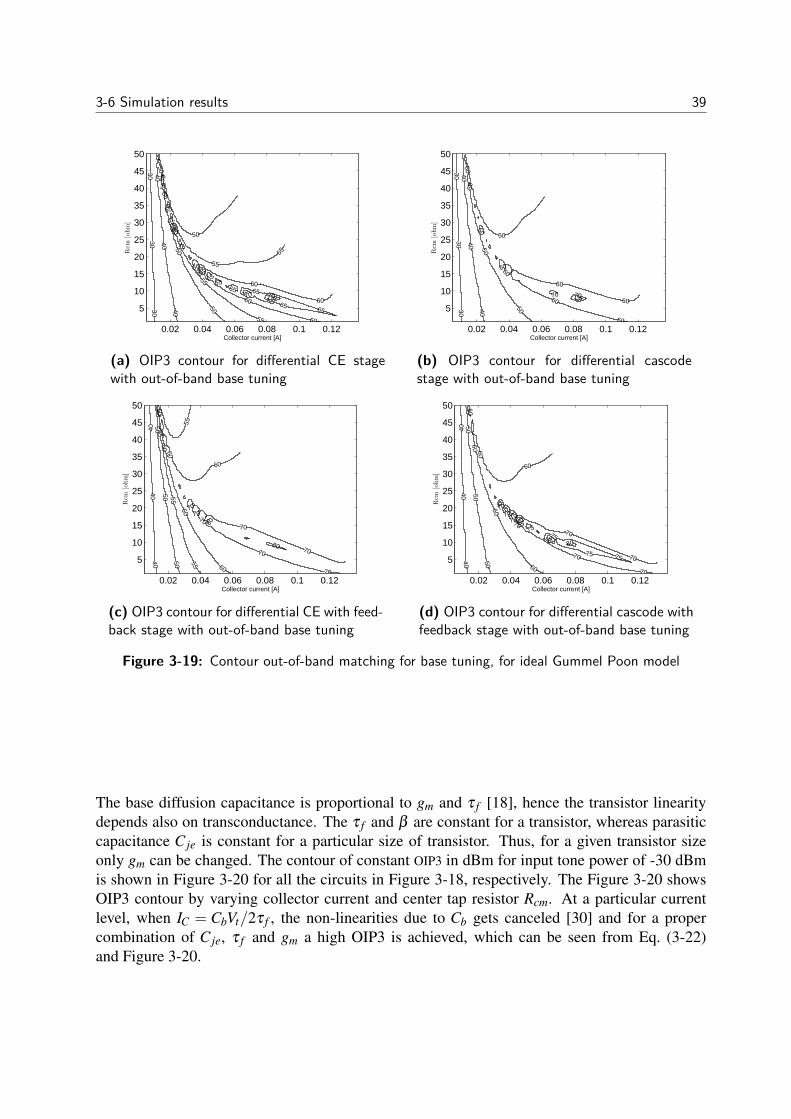
3-6 Simulation results 39
3030
3040
40
40
50
50
50
50
50
55
55
55
55
55
55
55
55
55
60
60
60
60
60
60
60
65
65
65
6565
6565
7070 75
Collector current [A]
Rcm
[ohm]
0.02 0.04 0.06 0.08 0.1 0.12
5
10
15
20
25
30
35
40
45
50
(a) OIP3 contour for differential CE stagewith out-of-band base tuning
3030
3040
40
40
50
50
50
50
50
60
6060
60
60
60
60
7070 75
Collector current [A]
Rcm
[ohm]
0.02 0.04 0.06 0.08 0.1 0.12
5
10
15
20
25
30
35
40
45
50
(b) OIP3 contour for differential cascodestage with out-of-band base tuning
40
4040
5050
50
55
55
55
55
60
6060
60
60
60
70
7070
70
70
7070
80
80
Collector current [A]
Rcm
[ohm]
0.02 0.04 0.06 0.08 0.1 0.12
5
10
15
20
25
30
35
40
45
50
(c) OIP3 contour for differential CE with feed-back stage with out-of-band base tuning
40
4040
5050
50
60
6060
60
60
60
70
70
70
70
70
7070
70
75
75
75
75
7575
80
8080
Collector current [A]
Rcm
[ohm]
0.02 0.04 0.06 0.08 0.1 0.12
5
10
15
20
25
30
35
40
45
50
(d) OIP3 contour for differential cascode withfeedback stage with out-of-band base tuning
Figure 3-19: Contour out-of-band matching for base tuning, for ideal Gummel Poon model
The base diffusion capacitance is proportional to gm and τ f [18], hence the transistor linearitydepends also on transconductance. The τ f and β are constant for a transistor, whereas parasiticcapacitance C je is constant for a particular size of transistor. Thus, for a given transistor sizeonly gm can be changed. The contour of constant OIP3 in dBm for input tone power of -30 dBmis shown in Figure 3-20 for all the circuits in Figure 3-18, respectively. The Figure 3-20 showsOIP3 contour by varying collector current and center tap resistor Rcm. At a particular currentlevel, when IC = CbVt/2τ f , the non-linearities due to Cb gets canceled [30] and for a propercombination of C je, τ f and gm a high OIP3 is achieved, which can be seen from Eq. (3-22)and Figure 3-20.
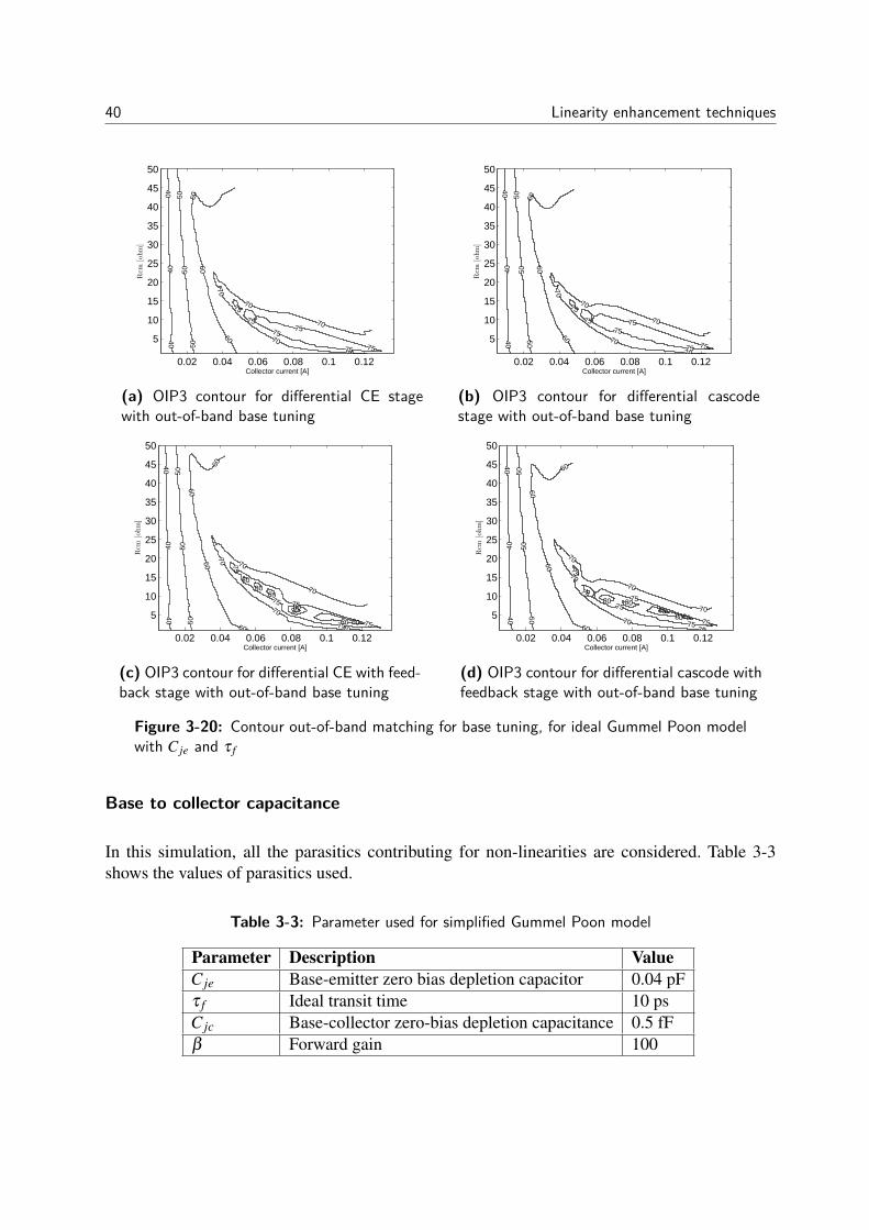
40 Linearity enhancement techniques
40
40
40
5050
5060
60
60
70
70
70
70
7075
7575
75
75
75
Collector current [A]
Rcm
[ohm]
0.02 0.04 0.06 0.08 0.1 0.12
5
10
15
20
25
30
35
40
45
50
(a) OIP3 contour for differential CE stagewith out-of-band base tuning
40
40
40
5050
50
60
60
60
70
7070
70
7075
7575
75
75
75
Collector current [A]
Rcm
[ohm]
0.02 0.04 0.06 0.08 0.1 0.12
5
10
15
20
25
30
35
40
45
50
(b) OIP3 contour for differential cascodestage with out-of-band base tuning
40
40
40
5050
50
60
60
60
60
70
70
70
70
7075
75
75
75
7580 80
80
8080
80
85
Collector current [A]
Rcm
[ohm]
0.02 0.04 0.06 0.08 0.1 0.12
5
10
15
20
25
30
35
40
45
50
(c) OIP3 contour for differential CE with feed-back stage with out-of-band base tuning
40
40
40
5050
50
60
60
60
60
70
70
70
70
7070
75
7575
75
7575
8080
808085
Collector current [A]
Rcm
[ohm]
0.02 0.04 0.06 0.08 0.1 0.12
5
10
15
20
25
30
35
40
45
50
(d) OIP3 contour for differential cascode withfeedback stage with out-of-band base tuning
Figure 3-20: Contour out-of-band matching for base tuning, for ideal Gummel Poon modelwith C je and τ f
Base to collector capacitance
In this simulation, all the parasitics contributing for non-linearities are considered. Table 3-3shows the values of parasitics used.
Table 3-3: Parameter used for simplified Gummel Poon model
Parameter Description ValueC je Base-emitter zero bias depletion capacitor 0.04 pFτ f Ideal transit time 10 psC jc Base-collector zero-bias depletion capacitance 0.5 fFβ Forward gain 100
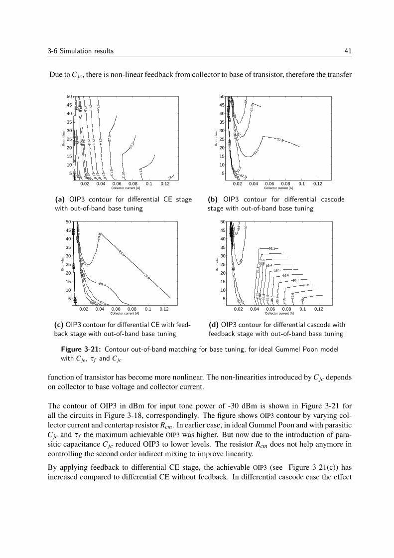
3-6 Simulation results 41
Due to C jc, there is non-linear feedback from collector to base of transistor, therefore the transfer
27
27.1
27.2
27.2
27.3
27.3
27.427.4
27.4
27.527.5
27.5
27.627.6
27.6
27.827.8
27.8
27.927.9
27.9
2828
28
2929
2929
3030
30
3030
34
3434
Collector current [A]
Rcm
[ohm]
0.02 0.04 0.06 0.08 0.1 0.12
5
10
15
20
25
30
35
40
45
50
(a) OIP3 contour for differential CE stagewith out-of-band base tuning
32
32
3232
32
32.1
32.1
32.1
32.1
32.1
32.1
32.2
32.2
32.2
32.232.2
32.2
32.2
32.3
32.3
32.3
32.332.334
34
35
Collector current [A]
Rcm
[ohm]
0.02 0.04 0.06 0.08 0.1 0.12
5
10
15
20
25
30
35
40
45
50
(b) OIP3 contour for differential cascodestage with out-of-band base tuning
2828
28
29.6
29.6
29.6
29.6
29.6
29.629.6
29.629.7
29.729.7
29.729.7
29.7
29.829.8
29.829.8
29.8
29.8
29.929.9
29.929.9
29.9
29.9
3030
3030
30
30
Collector current [A]
Rcm
[ohm]
0.02 0.04 0.06 0.08 0.1 0.12
5
10
15
20
25
30
35
40
45
50
(c) OIP3 contour for differential CE with feed-back stage with out-of-band base tuning
3434
34
34
3535
35
35
35
3536.1
36.1
36.136.1
36.2
36.2
36.236.2
36.3
36.3
36.336.3
36.436
.4
36.436.4
36.536
.5
36.5
36.636
.6
36.6
36.736
.7
36.7
36.8
36.8
36.8
36.9
36.9
37
37
Collector current [A]
Rcm
[ohm]
0.02 0.04 0.06 0.08 0.1 0.12
5
10
15
20
25
30
35
40
45
50
(d) OIP3 contour for differential cascode withfeedback stage with out-of-band base tuning
Figure 3-21: Contour out-of-band matching for base tuning, for ideal Gummel Poon modelwith C je, τ f and C jc
function of transistor has become more nonlinear. The non-linearities introduced by C jc dependson collector to base voltage and collector current.
The contour of OIP3 in dBm for input tone power of -30 dBm is shown in Figure 3-21 forall the circuits in Figure 3-18, correspondingly. The figure shows OIP3 contour by varying col-lector current and centertap resistor Rcm. In earlier case, in ideal Gummel Poon and with parasiticC je and τ f the maximum achievable OIP3 was higher. But now due to the introduction of para-sitic capacitance C jc reduced OIP3 to lower levels. The resistor Rcm does not help anymore incontrolling the second order indirect mixing to improve linearity.
By applying feedback to differential CE stage, the achievable OIP3 (see Figure 3-21(c)) hasincreased compared to differential CE without feedback. In differential cascode case the effect
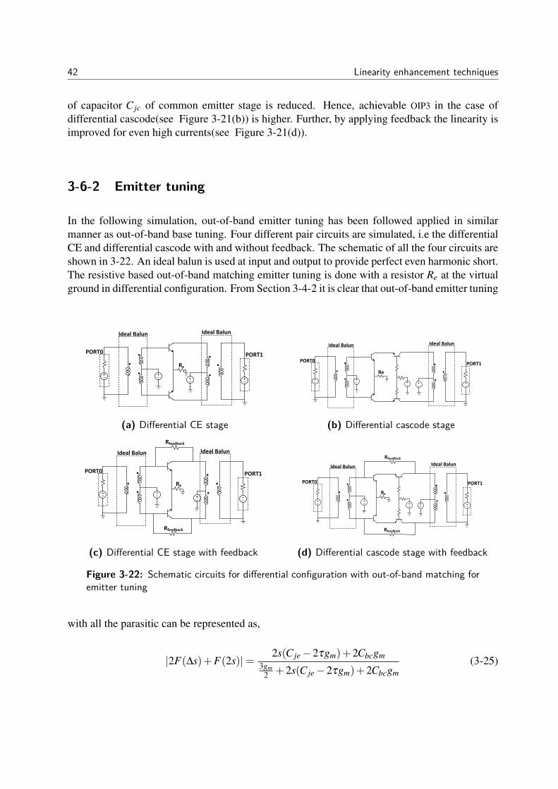
42 Linearity enhancement techniques
of capacitor C jc of common emitter stage is reduced. Hence, achievable OIP3 in the case ofdifferential cascode(see Figure 3-21(b)) is higher. Further, by applying feedback the linearity isimproved for even high currents(see Figure 3-21(d)).
3-6-2 Emitter tuning
In the following simulation, out-of-band emitter tuning has been followed applied in similarmanner as out-of-band base tuning. Four different pair circuits are simulated, i.e the differentialCE and differential cascode with and without feedback. The schematic of all the four circuits areshown in 3-22. An ideal balun is used at input and output to provide perfect even harmonic short.The resistive based out-of-band matching emitter tuning is done with a resistor Re at the virtualground in differential configuration. From Section 3-4-2 it is clear that out-of-band emitter tuning
PORT1PORT0
Ideal Balun Ideal Balun
Re
(a) Differential CE stage
r
r
PORT1PORT0
Ideal Balun Ideal Balun
Re
(b) Differential cascode stage
PORT1PORT0
Ideal Balun Ideal Balun
Re
Rfeedback
Rfeedback
(c) Differential CE stage with feedback
r
r
PORT1PORT0
Ideal Balun Ideal Balun
Rfeedback
Rfeedback
Re
(d) Differential cascode stage with feedback
Figure 3-22: Schematic circuits for differential configuration with out-of-band matching foremitter tuning
with all the parasitic can be represented as,
|2F(∆s)+F(2s)|=2s(C je−2τgm)+2Cbcgm
3gm2 +2s(C je−2τgm)+2Cbcgm
(3-25)
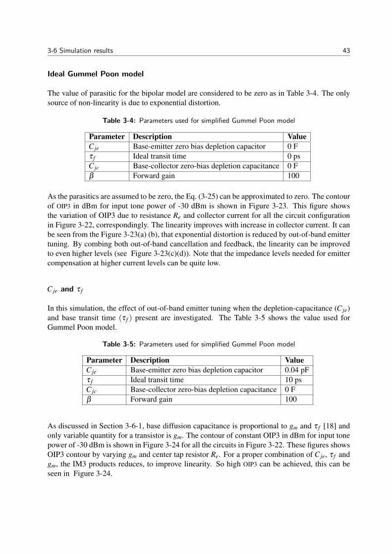
3-6 Simulation results 43
Ideal Gummel Poon model
The value of parasitic for the bipolar model are considered to be zero as in Table 3-4. The onlysource of non-linearity is due to exponential distortion.
Table 3-4: Parameters used for simplified Gummel Poon model
Parameter Description ValueC je Base-emitter zero bias depletion capacitor 0 Fτ f Ideal transit time 0 psC jc Base-collector zero-bias depletion capacitance 0 Fβ Forward gain 100
As the parasitics are assumed to be zero, the Eq. (3-25) can be approximated to zero. The contourof OIP3 in dBm for input tone power of -30 dBm is shown in Figure 3-23. This figure showsthe variation of OIP3 due to resistance Re and collector current for all the circuit configurationin Figure 3-22, correspondingly. The linearity improves with increase in collector current. It canbe seen from the Figure 3-23(a) (b), that exponential distortion is reduced by out-of-band emittertuning. By combing both out-of-band cancellation and feedback, the linearity can be improvedto even higher levels (see Figure 3-23(c)(d)). Note that the impedance levels needed for emittercompensation at higher current levels can be quite low.
C je and τ f
In this simulation, the effect of out-of-band emitter tuning when the depletion-capacitance (C je)and base transit time (τ f ) present are investigated. The Table 3-5 shows the value used forGummel Poon model.
Table 3-5: Parameters used for simplified Gummel Poon model
Parameter Description ValueC je Base-emitter zero bias depletion capacitor 0.04 pFτ f Ideal transit time 10 psC jc Base-collector zero-bias depletion capacitance 0 Fβ Forward gain 100
As discussed in Section 3-6-1, base diffusion capacitance is proportional to gm and τ f [18] andonly variable quantity for a transistor is gm. The contour of constant OIP3 in dBm for input tonepower of -30 dBm is shown in Figure 3-24 for all the circuits in Figure 3-22. These figures showsOIP3 contour by varying gm and center tap resistor Re. For a proper combination of C je, τ f andgm, the IM3 products reduces, to improve linearity. So high OIP3 can be achieved, this can beseen in Figure 3-24.
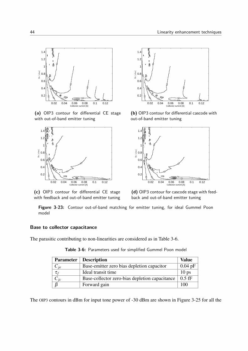
44 Linearity enhancement techniques
3030
40
40
4040
40
40
4040
50
50
50
50 60
6060
60
606565 70 75
Collector current [A]
Re[ohm]
0.02 0.04 0.06 0.08 0.1 0.12
0.2
0.4
0.6
0.8
1
1.2
1.4
(a) OIP3 contour for differential CE stagewith out-of-band emitter tuning
3030
40
40
4040
4040
4040
50
50
50
50 60
6060
6060
70 75
Collector current [A]
Re[ohm]
0.02 0.04 0.06 0.08 0.1 0.12
0.2
0.4
0.6
0.8
1
1.2
1.4
(b) OIP3 contour for differential cascode without-of-band emitter tuning
4040
4040
4040
50
50
5050
5050
50
60
6060
60
60
60
7070
70 70
7080
Collector current [A]
Re[ohm]
0.02 0.04 0.06 0.08 0.1 0.12
0.2
0.4
0.6
0.8
1
1.2
1.4
(c) OIP3 contour for differential CE stagewith feedback and out-of-band emitter tuning
4040
40
40
4040
50
50
5050
5050
50
50
60
6060
60
60
60
7070
70 70
707580
Collector current [A]
Re[ohm]
0.02 0.04 0.06 0.08 0.1 0.12
0.2
0.4
0.6
0.8
1
1.2
1.4
(d) OIP3 contour for cascode stage with feed-back and out-of-band emitter tuning
Figure 3-23: Contour out-of-band matching for emitter tuning, for ideal Gummel Poonmodel
Base to collector capacitance
The parasitic contributing to non-linearities are considered as in Table 3-6.
Table 3-6: Parameters used for simplified Gummel Poon model
Parameter Description ValueC je Base-emitter zero bias depletion capacitor 0.04 pFτ f Ideal transit time 10 psC jc Base-collector zero-bias depletion capacitance 0.5 fFβ Forward gain 100
The OIP3 contours in dBm for input tone power of -30 dBm are shown in Figure 3-25 for all the
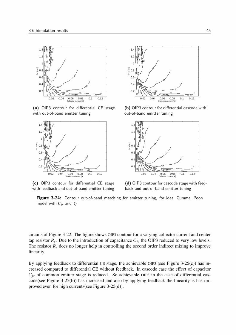
3-6 Simulation results 45
25
30
3030
30
35
35
35
35
35
35
35
35
35
35
35
35
35
40
40
40
40
40
45
45
45
45
50
5050
505555
55 55
5560
Collector current [A]
Re[ohm]
0.02 0.04 0.06 0.08 0.1 0.12
0.2
0.4
0.6
0.8
1
1.2
1.4
(a) OIP3 contour for differential CE stagewith out-of-band emitter tuning
2525
25
30
3030
30
30
30
35
35
35
35
35
35
35
3535
40
40
40
40
40
45
45
45
45
505050
5055
5555 55
5560
Collector current [A]
Re[ohm]
0.02 0.04 0.06 0.08 0.1 0.12
0.2
0.4
0.6
0.8
1
1.2
1.4
(b) OIP3 contour for differential cascode without-of-band emitter tuning
2525
3030
30
3030
35
35
35
35
3535
35
35
35
3535
40
40
40
40
40
45
45
45
45
50
5050
50
555555
55606060
Collector current [A]
Re[ohm]
0.02 0.04 0.06 0.08 0.1 0.12
0.2
0.4
0.6
0.8
1
1.2
1.4
(c) OIP3 contour for differential CE stagewith feedback and out-of-band emitter tuning
20
2020
2525
2530
30
3030
3030
30
35
35
3535
3535
3535
40
40
40
40
45
45
45
50
5050
50
50
5555 55
5560
Collector current [A]
Re[ohm]
0.02 0.04 0.06 0.08 0.1 0.12
0.2
0.4
0.6
0.8
1
1.2
1.4
(d) OIP3 contour for cascode stage with feed-back and out-of-band emitter tuning
Figure 3-24: Contour out-of-band matching for emitter tuning, for ideal Gummel Poonmodel with C je and τ f
circuits of Figure 3-22. The figure shows OIP3 contour for a varying collector current and centertap resistor Re. Due to the introduction of capacitance C jc the OIP3 reduced to very low levels.The resistor Re does no longer help in controlling the second order indirect mixing to improvelinearity.
By applying feedback to differential CE stage, the achievable OIP3 (see Figure 3-25(c)) has in-creased compared to differential CE without feedback. In cascode case the effect of capacitorC jc of common emitter stage is reduced. So achievable OIP3 in the case of differential cas-code(see Figure 3-25(b)) has increased and also by applying feedback the linearity is has im-proved even for high currents(see Figure 3-25(d)).
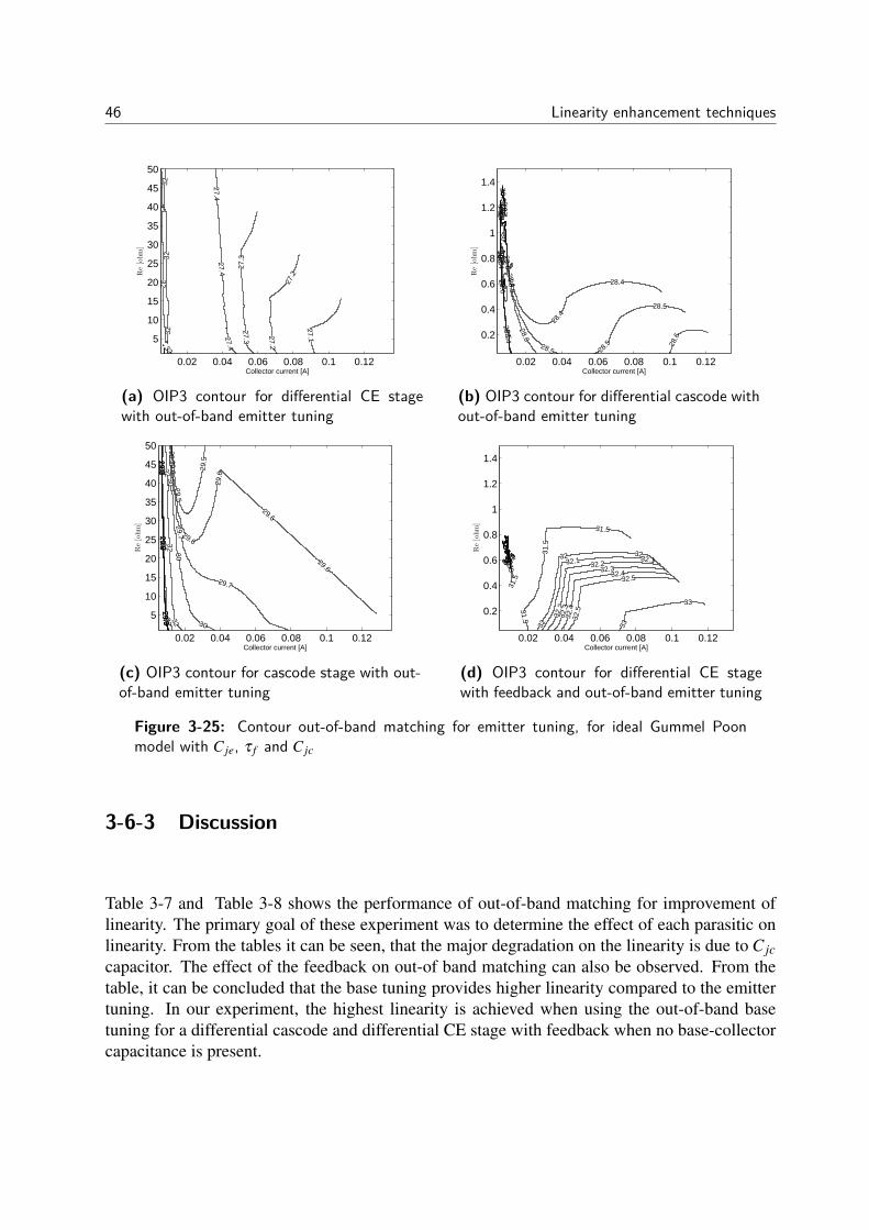
46 Linearity enhancement techniques
27.1
27.2
27.2
27.3
27.3
27.427.4
27.4
3232
3232
32
32
Collector current [A]
Re[ohm]
0.02 0.04 0.06 0.08 0.1 0.12
5
10
15
20
25
30
35
40
45
50
(a) OIP3 contour for differential CE stagewith out-of-band emitter tuning
28.4
28.4
28.4
28.428.4
28.428.4
28.5
28.5
28.528.5
28.528.5
28.5
28.5
28.6
28.6
28.6
28.6
28.6
28.630
3030
31Collector current [A]
Re[ohm]
0.02 0.04 0.06 0.08 0.1 0.12
0.2
0.4
0.6
0.8
1
1.2
1.4
(b) OIP3 contour for differential cascode without-of-band emitter tuning
29.529.5
29.5
29.5
29.5
29.6
29.6
29.6
29.6
29.6
29.629.6
29.629.7
29.729.7
29.729.7
29.7
3030
3030
30
30
3232
3232
3232
Collector current [A]
Re[ohm]
0.02 0.04 0.06 0.08 0.1 0.12
5
10
15
20
25
30
35
40
45
50
(c) OIP3 contour for cascode stage with out-of-band emitter tuning
31.5
31.5
31.5
31.531.5
31.5
3232
32
32
32 32.132.1
32.132.1 32.2
32.2
32.2
32.2
32.332
.3
32.3
32.3
32.432
.4
32.4
32.4
32.532
.5
32.5
32.5
33
33
33
33
Collector current [A]
Re[ohm]
0.02 0.04 0.06 0.08 0.1 0.12
0.2
0.4
0.6
0.8
1
1.2
1.4
(d) OIP3 contour for differential CE stagewith feedback and out-of-band emitter tuning
Figure 3-25: Contour out-of-band matching for emitter tuning, for ideal Gummel Poonmodel with C je, τ f and C jc
3-6-3 Discussion
Table 3-7 and Table 3-8 shows the performance of out-of-band matching for improvement oflinearity. The primary goal of these experiment was to determine the effect of each parasitic onlinearity. From the tables it can be seen, that the major degradation on the linearity is due to C jccapacitor. The effect of the feedback on out-of band matching can also be observed. From thetable, it can be concluded that the base tuning provides higher linearity compared to the emittertuning. In our experiment, the highest linearity is achieved when using the out-of-band basetuning for a differential cascode and differential CE stage with feedback when no base-collectorcapacitance is present.
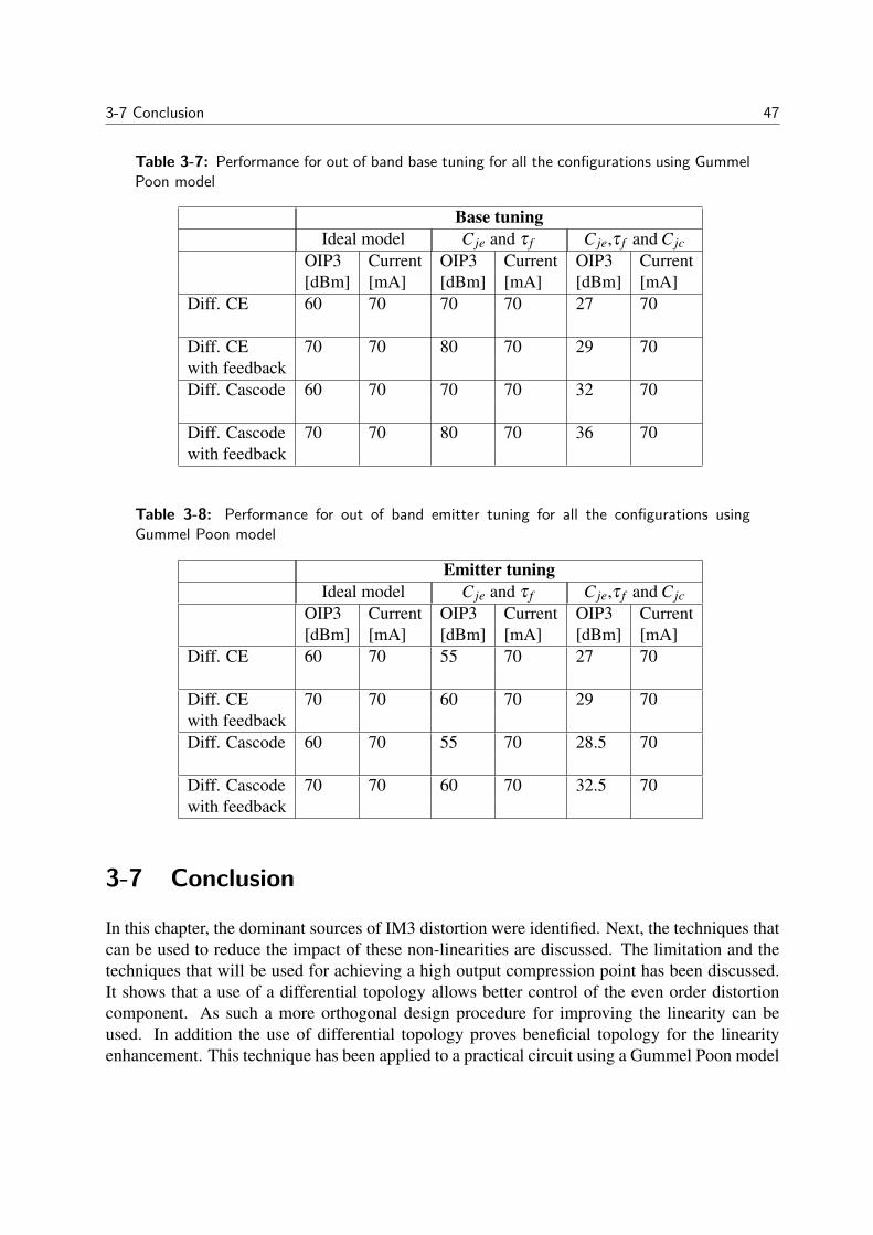
3-7 Conclusion 47
Table 3-7: Performance for out of band base tuning for all the configurations using GummelPoon model
Base tuningIdeal model C je and τ f C je,τ f and C jc
OIP3 Current OIP3 Current OIP3 Current[dBm] [mA] [dBm] [mA] [dBm] [mA]
Diff. CE 60 70 70 70 27 70
Diff. CE 70 70 80 70 29 70with feedbackDiff. Cascode 60 70 70 70 32 70
Diff. Cascode 70 70 80 70 36 70with feedback
Table 3-8: Performance for out of band emitter tuning for all the configurations usingGummel Poon model
Emitter tuningIdeal model C je and τ f C je,τ f and C jc
OIP3 Current OIP3 Current OIP3 Current[dBm] [mA] [dBm] [mA] [dBm] [mA]
Diff. CE 60 70 55 70 27 70
Diff. CE 70 70 60 70 29 70with feedbackDiff. Cascode 60 70 55 70 28.5 70
Diff. Cascode 70 70 60 70 32.5 70with feedback
3-7 Conclusion
In this chapter, the dominant sources of IM3 distortion were identified. Next, the techniques thatcan be used to reduce the impact of these non-linearities are discussed. The limitation and thetechniques that will be used for achieving a high output compression point has been discussed.It shows that a use of a differential topology allows better control of the even order distortioncomponent. As such a more orthogonal design procedure for improving the linearity can beused. In addition the use of differential topology proves beneficial topology for the linearityenhancement. This technique has been applied to a practical circuit using a Gummel Poon model

48 Linearity enhancement techniques
for the active device. From the results, it can be concluded that the base collector capacitance isthe major constrain in achieving high linearity
Chapter 4
A two stage low noise and highly linearLNA
4-1 Introduction
In a two stage design, the input stage should have low noise, high gain, and low return loss whilethe output stage should have high linearity and high compression point. In this chapter the im-plementation details of both the input and output stages designed in this work are presented. Thelinearity and compression point enhancement techniques discussed in chapter 3 are employedand the schematic level simulation results are presented.
The design and implementations of the input stage is discussed in Section 4-2. In next Section 4-3, two differential implementation of the output stage using linearity enhancement technique arepresented. In last Section 4-4, both the input stage and the output stage are combined to form acomplete two stage LNA .
4-2 Input stage
As discussed in Chapter 2, the input stage of the LNA is targeted for high gain, low noise andlinearity requirements. The high gain is achieved by using a cascade of CE-CB stage, whichis normally referred as cascode. This also improves reverse isolation. A low noise figure isachieved by selecting proper transistor biasing and noise matching. The linearity is improvedto some extent by using inductive degeneration. The other important requirement is low returnloss, because the duplexer filter preceding the LNA is sensitive to load matching. The filterbetween antenna and LNA is designed as high frequency device with a load termination of 50Ω. If the load termination deviates from 50 Ω, the filter may have losses and show ripple effect
Master of Science Thesis 49 Sanganagouda B Patil
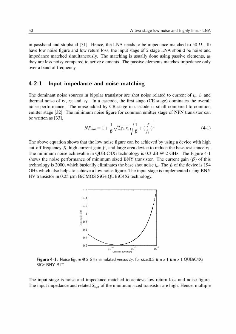
50 A two stage low noise and highly linear LNA
in passband and stopband [31]. Hence, the LNA needs to be impedance matched to 50 Ω. Tohave low noise figure and low return loss, the input stage of 2 stage LNA should be noise andimpedance matched simultaneously. The matching is usually done using passive elements, asthey are less noisy compared to active elements. The passive elements matches impedance onlyover a band of frequency.
4-2-1 Input impedance and noise matching
The dominant noise sources in bipolar transistor are shot noise related to current of ib, ic andthermal noise of rb, rE and, rC. In a cascode, the first stage (CE stage) dominates the overallnoise performance. The noise added by CB stage in cascode is small compared to commonemitter stage [32]. The minimum noise figure for common emitter stage of NPN transistor canbe written as [33],
NFmin = 1+1β
√2gmrb
√1β+(
ffT)2 (4-1)
The above equation shows that the low noise figure can be achieved by using a device with highcut-off frequency ft , high current gain β , and large area device to reduce the base resistance rb.The minimum noise achievable in QUBiC4Xi technology is 0.3 dB @ 2 GHz. The Figure 4-1shows the noise performance of minimum sized BNY transistor. The current gain (β ) of thistechnology is 2000, which basically eliminates the base shot noise ib. The ft of the device is 194GHz which also helps to achieve a low noise figure. The input stage is implemented using BNYHV transistor in 0.25 µm BiCMOS SiGe QUBiC4Xi technology.
10−4
10−3
10−2
0.2
0.4
0.6
0.8
1
1.2
1.4
1.6
Noisefigure
[dB]
Collector current [A]
Figure 4-1: Noise figure @ 2 GHz simulated versus IC, for size:0.3 µm x 1 µm x 1 QUBiC4XiSiGe BNY BJT
The input stage is noise and impedance matched to achieve low return loss and noise figure.The input impedance and related Sopt of the minimum sized transistor are high. Hence, multiple
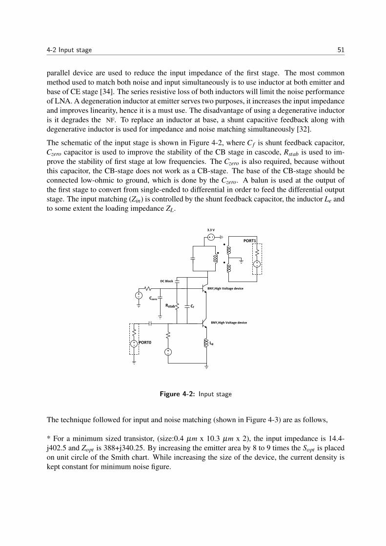
4-2 Input stage 51
parallel device are used to reduce the input impedance of the first stage. The most commonmethod used to match both noise and input simultaneously is to use inductor at both emitter andbase of CE stage [34]. The series resistive loss of both inductors will limit the noise performanceof LNA. A degeneration inductor at emitter serves two purposes, it increases the input impedanceand improves linearity, hence it is a must use. The disadvantage of using a degenerative inductoris it degrades the NF. To replace an inductor at base, a shunt capacitive feedback along withdegenerative inductor is used for impedance and noise matching simultaneously [32].
The schematic of the input stage is shown in Figure 4-2, where C f is shunt feedback capacitor,Czero capacitor is used to improve the stability of the CB stage in cascode, Rstab is used to im-prove the stability of first stage at low frequencies. The Czero is also required, because withoutthis capacitor, the CB-stage does not work as a CB-stage. The base of the CB-stage should beconnected low-ohmic to ground, which is done by the Czero. A balun is used at the output ofthe first stage to convert from single-ended to differential in order to feed the differential outputstage. The input matching (Zin) is controlled by the shunt feedback capacitor, the inductor Le andto some extent the loading impedance ZL.
BNY,High Voltage device
PORT0
PORT1
BNY,High Voltage device
3.3 V
Cf
Le
Rstab
DC Block
Czero
Figure 4-2: Input stage
The technique followed for input and noise matching (shown in Figure 4-3) are as follows,
* For a minimum sized transistor, (size:0.4 µm x 10.3 µm x 2), the input impedance is 14.4-j402.5 and Zopt is 388+j340.25. By increasing the emitter area by 8 to 9 times the Sopt is placedon unit circle of the Smith chart. While increasing the size of the device, the current density iskept constant for minimum noise figure.
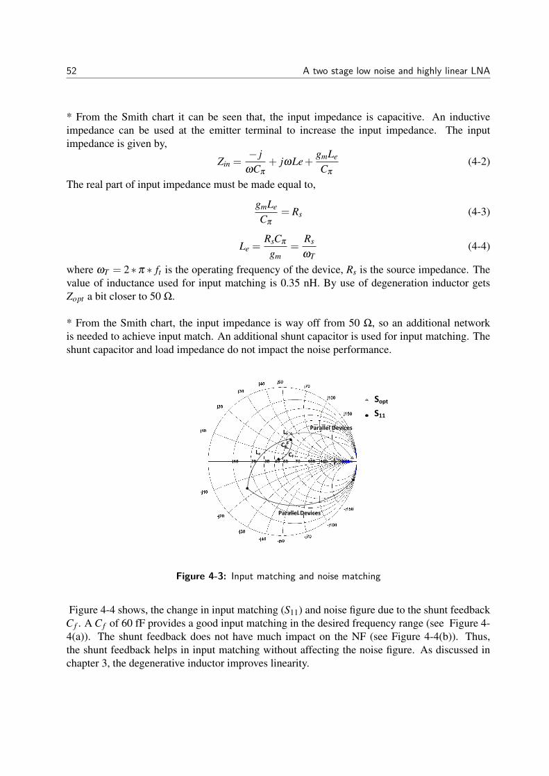
52 A two stage low noise and highly linear LNA
* From the Smith chart it can be seen that, the input impedance is capacitive. An inductiveimpedance can be used at the emitter terminal to increase the input impedance. The inputimpedance is given by,
Zin =− j
ωCπ
+ jωLe+gmLe
Cπ
(4-2)
The real part of input impedance must be made equal to,
gmLe
Cπ
= Rs (4-3)
Le =RsCπ
gm=
Rs
ωT(4-4)
where ωT = 2∗π ∗ ft is the operating frequency of the device, Rs is the source impedance. Thevalue of inductance used for input matching is 0.35 nH. By use of degeneration inductor getsZopt a bit closer to 50 Ω.
* From the Smith chart, the input impedance is way off from 50 Ω, so an additional networkis needed to achieve input match. An additional shunt capacitor is used for input matching. Theshunt capacitor and load impedance do not impact the noise performance.
Sopt
S11
Parallel Devices
Parallel Devices
Le
Le
Cf
Cf
Figure 4-3: Input matching and noise matching
Figure 4-4 shows, the change in input matching (S11) and noise figure due to the shunt feedbackC f . A C f of 60 fF provides a good input matching in the desired frequency range (see Figure 4-4(a)). The shunt feedback does not have much impact on the NF (see Figure 4-4(b)). Thus,the shunt feedback helps in input matching without affecting the noise figure. As discussed inchapter 3, the degenerative inductor improves linearity.
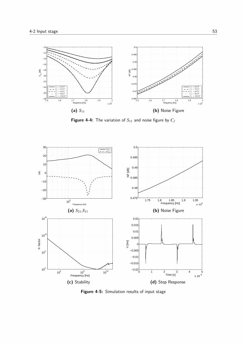
4-2 Input stage 53
1.5 1.6 1.7 1.8 1.9 2
x 109
−28
−26
−24
−22
−20
−18
−16
−14
−12
−10
frequency [Hz]
S11
[dB
]
Cf = 60fFCf = 70fFCf = 80fFCf = 90fFCf = 100fF
(a) S11
1.5 1.6 1.7 1.8 1.9 2
x 109
0.465
0.47
0.475
0.48
0.485
0.49
0.495
0.5
frequency [Hz]
NF
[dB
]
Cf = 60fFCf = 70fFCf = 80fFCf = 90fFCf = 100fF
(b) Noise Figure
Figure 4-4: The variation of S11 and noise figure by C f
109
−30
−20
−10
0
10
20
30
Frequency [Hz]
[dB
]
s21s11
(a) S21,S11
1.75 1.8 1.85 1.9 1.95
x 109
0.475
0.48
0.485
0.49
0.495
0.5
Frequency [Hz]
NF
[dB
]
(b) Noise Figure
106
108
1010
100
105
1010
1015
Frequency [Hz]
K−
fact
or
(c) Stability
0 1 2 3 4 5
x 10−8
−0.02
−0.015
−0.01
−0.005
0
0.005
0.01
0.015
0.02
Time [s]
V [m
v]
(d) Step Response
Figure 4-5: Simulation results of input stage
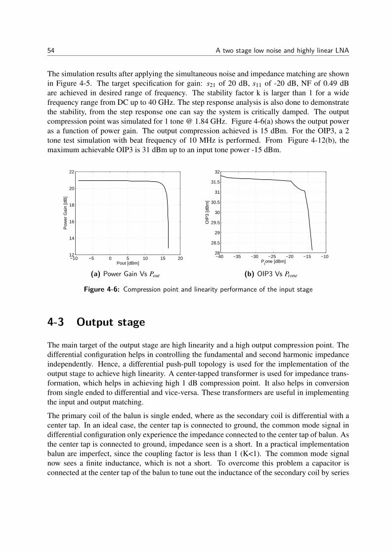
54 A two stage low noise and highly linear LNA
The simulation results after applying the simultaneous noise and impedance matching are shownin Figure 4-5. The target specification for gain: s21 of 20 dB, s11 of -20 dB, NF of 0.49 dBare achieved in desired range of frequency. The stability factor k is larger than 1 for a widefrequency range from DC up to 40 GHz. The step response analysis is also done to demonstratethe stability, from the step response one can say the system is critically damped. The outputcompression point was simulated for 1 tone @ 1.84 GHz. Figure 4-6(a) shows the output poweras a function of power gain. The output compression achieved is 15 dBm. For the OIP3, a 2tone test simulation with beat frequency of 10 MHz is performed. From Figure 4-12(b), themaximum achievable OIP3 is 31 dBm up to an input tone power -15 dBm.
−10 −5 0 5 10 15 2012
14
16
18
20
22
Pout [dBm]
Pow
er G
ain
[dB
]
(a) Power Gain Vs Pout
−40 −35 −30 −25 −20 −15 −1028
28.5
29
29.5
30
30.5
31
31.5
32
Ptone [dBm]
OIP
3 [d
Bm
]
(b) OIP3 Vs Ptone
Figure 4-6: Compression point and linearity performance of the input stage
4-3 Output stage
The main target of the output stage are high linearity and a high output compression point. Thedifferential configuration helps in controlling the fundamental and second harmonic impedanceindependently. Hence, a differential push-pull topology is used for the implementation of theoutput stage to achieve high linearity. A center-tapped transformer is used for impedance trans-formation, which helps in achieving high 1 dB compression point. It also helps in conversionfrom single ended to differential and vice-versa. These transformers are useful in implementingthe input and output matching.
The primary coil of the balun is single ended, where as the secondary coil is differential with acenter tap. In an ideal case, the center tap is connected to ground, the common mode signal indifferential configuration only experience the impedance connected to the center tap of balun. Asthe center tap is connected to ground, impedance seen is a short. In a practical implementationbalun are imperfect, since the coupling factor is less than 1 (K<1). The common mode signalnow sees a finite inductance, which is not a short. To overcome this problem a capacitor isconnected at the center tap of the balun to tune out the inductance of the secondary coil by series
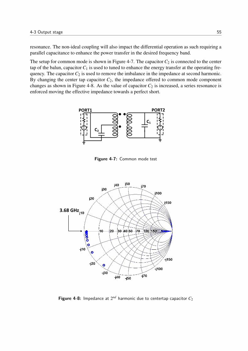
4-3 Output stage 55
resonance. The non-ideal coupling will also impact the differential operation as such requiring aparallel capacitance to enhance the power transfer in the desired frequency band.
The setup for common mode is shown in Figure 4-7. The capacitor C2 is connected to the centertap of the balun, capacitor C1 is used to tuned to enhance the energy transfer at the operating fre-quency. The capacitor C2 is used to remove the imbalance in the impedance at second harmonic.By changing the center tap capacitor C2, the impedance offered to common mode componentchanges as shown in Figure 4-8. As the value of capacitor C2 is increased, a series resonance isenforced moving the effective impedance towards a perfect short.
PORT2
C1
C2
PORT1
Figure 4-7: Common mode test
3.68 GHz
Figure 4-8: Impedance at 2nd harmonic due to centertap capacitor C2
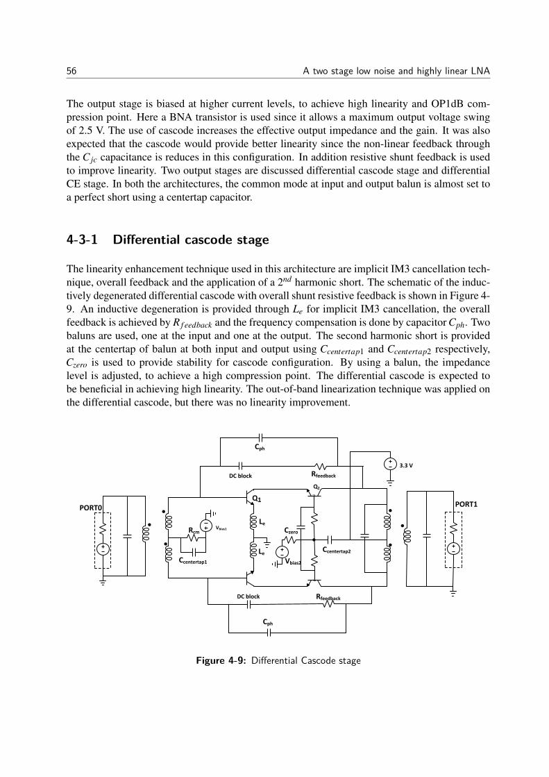
56 A two stage low noise and highly linear LNA
The output stage is biased at higher current levels, to achieve high linearity and OP1dB com-pression point. Here a BNA transistor is used since it allows a maximum output voltage swingof 2.5 V. The use of cascode increases the effective output impedance and the gain. It was alsoexpected that the cascode would provide better linearity since the non-linear feedback throughthe C jc capacitance is reduces in this configuration. In addition resistive shunt feedback is usedto improve linearity. Two output stages are discussed differential cascode stage and differentialCE stage. In both the architectures, the common mode at input and output balun is almost set toa perfect short using a centertap capacitor.
4-3-1 Differential cascode stage
The linearity enhancement technique used in this architecture are implicit IM3 cancellation tech-nique, overall feedback and the application of a 2nd harmonic short. The schematic of the induc-tively degenerated differential cascode with overall shunt resistive feedback is shown in Figure 4-9. An inductive degeneration is provided through Le for implicit IM3 cancellation, the overallfeedback is achieved by R f eedback and the frequency compensation is done by capacitor Cph. Twobaluns are used, one at the input and one at the output. The second harmonic short is providedat the centertap of balun at both input and output using Ccentertap1 and Ccentertap2 respectively,Czero is used to provide stability for cascode configuration. By using a balun, the impedancelevel is adjusted, to achieve a high compression point. The differential cascode is expected tobe beneficial in achieving high linearity. The out-of-band linearization technique was applied onthe differential cascode, but there was no linearity improvement.
r
r
3.3 V
PORT1PORT0
Ccentertap2
Ccentertap1
CzeroVbias1
Vbias2
Le
Le
Rcm
Cph
Cph
DC block
DC block Rfeedback
Rfeedback
Q1
Q2
Figure 4-9: Differential Cascode stage
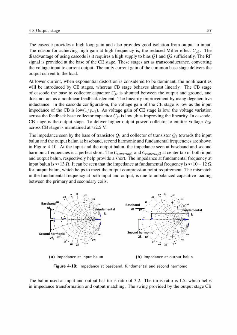
4-3 Output stage 57
The cascode provides a high loop gain and also provides good isolation from output to input.The reason for achieving high gain at high frequency is, the reduced Miller effect Cµ1. Thedisadvantage of using cascode is it requires a high supply to bias Q1 and Q2 sufficiently. The RFsignal is provided at the base of the CE stage. These stages act as transconductance, convertingthe voltage input to current output. The unity current gain of the common base stage delivers theoutput current to the load.
At lower current, when exponential distortion is considered to be dominant, the nonlinearitieswill be introduced by CE stages, whereas CB stage behaves almost linearly. The CB stageof cascode the base to collector capacitor C jc is shunted between the output and ground, anddoes not act as a nonlinear feedback element. The linearity improvement by using degenerativeinductance. In the cascode configuration, the voltage gain of the CE stage is low as the inputimpedance of the CB is low(1/gm2). As voltage gain of CE stage is low, the voltage variationacross the feedback base collector capacitor C jc is low ,thus improving the linearity. In cascode,CB stage is the output stage. To deliver higher output power, collector to emitter voltage VCEacross CB stage is maintained at ≈2.5 V.
The impedance seen by the base of transistor Q1 and collector of transistor Q2 towards the inputbalun and the output balun at baseband, second harmonic and fundamental frequencies are shownin Figure 4-10. At the input and the output balun, the impedance seen at baseband and secondharmonic frequencies is a perfect short. The Ccentertap1 and Ccentertap2 at center tap of both inputand output balun, respectively help provide a short. The impedance at fundamental frequency atinput balun is≈ 13 Ω. It can be seen that the impedance at fundamental frequency is≈ 10−12 Ω
for output balun, which helps to meet the output compression point requirement. The mismatchin the fundamental frequency at both input and output, is due to unbalanced capacitive loadingbetween the primary and secondary coils.
Baseband Δf
Second harmonic 2f0
Fundamental f0
(a) Impedance at input balun
Baseband Δf
Second harmonic 2f0
Fundamental f0
(b) Impedance at output balun
Figure 4-10: Impedance at baseband, fundamental and second harmonic
The balun used at input and output has turns ratio of 3:2. The turns ratio is 1.5, which helpsin impedance transformation and output matching. The swing provided by the output stage CB
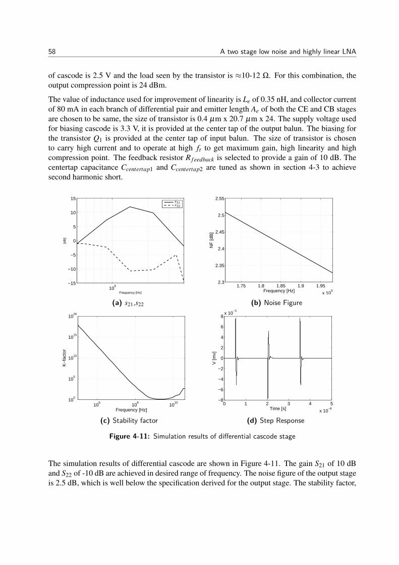
58 A two stage low noise and highly linear LNA
of cascode is 2.5 V and the load seen by the transistor is ≈10-12 Ω. For this combination, theoutput compression point is 24 dBm.
The value of inductance used for improvement of linearity is Le of 0.35 nH, and collector currentof 80 mA in each branch of differential pair and emitter length Ae of both the CE and CB stagesare chosen to be same, the size of transistor is 0.4 µm x 20.7 µm x 24. The supply voltage usedfor biasing cascode is 3.3 V, it is provided at the center tap of the output balun. The biasing forthe transistor Q1 is provided at the center tap of input balun. The size of transistor is chosento carry high current and to operate at high ft to get maximum gain, high linearity and highcompression point. The feedback resistor R f eedback is selected to provide a gain of 10 dB. Thecentertap capacitance Ccentertap1 and Ccentertap2 are tuned as shown in section 4-3 to achievesecond harmonic short.
109
−15
−10
−5
0
5
10
15
Frequency [Hz]
[dB
]
s21s22
(a) s21,s22
1.75 1.8 1.85 1.9 1.95
x 109
2.3
2.35
2.4
2.45
2.5
2.55
Frequency [Hz]
NF
[dB
]
(b) Noise Figure
106
108
1010
100
105
1010
1015
1020
Frequency [Hz]
K−
fact
or
(c) Stability factor
0 1 2 3 4 5
x 10−8
−8
−6
−4
−2
0
2
4
6
8x 10
−3
Time [s]
V [m
v]
(d) Step Response
Figure 4-11: Simulation results of differential cascode stage
The simulation results of differential cascode are shown in Figure 4-11. The gain S21 of 10 dBand S22 of -10 dB are achieved in desired range of frequency. The noise figure of the output stageis 2.5 dB, which is well below the specification derived for the output stage. The stability factor,
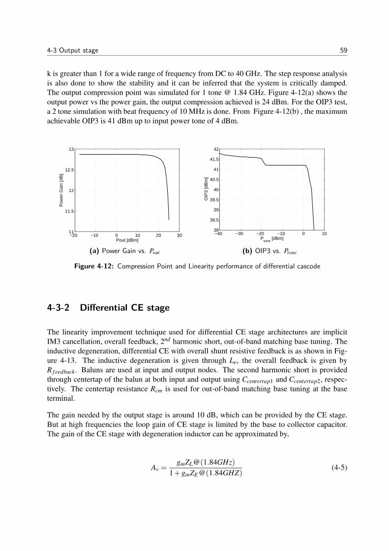
4-3 Output stage 59
k is greater than 1 for a wide range of frequency from DC to 40 GHz. The step response analysisis also done to show the stability and it can be inferred that the system is critically damped.The output compression point was simulated for 1 tone @ 1.84 GHz. Figure 4-12(a) shows theoutput power vs the power gain, the output compression achieved is 24 dBm. For the OIP3 test,a 2 tone simulation with beat frequency of 10 MHz is done. From Figure 4-12(b) , the maximumachievable OIP3 is 41 dBm up to input power tone of 4 dBm.
−20 −10 0 10 20 3011
11.5
12
12.5
13
Pout [dBm]
Pow
er G
ain
[dB
]
(a) Power Gain vs. Pout
−40 −30 −20 −10 0 1038
38.5
39
39.5
40
40.5
41
41.5
42
Ptone
[dBm]
OIP
3 [d
Bm
]
(b) OIP3 vs. Ptone
Figure 4-12: Compression Point and Linearity performance of differential cascode
4-3-2 Differential CE stage
The linearity improvement technique used for differential CE stage architectures are implicitIM3 cancellation, overall feedback, 2nd harmonic short, out-of-band matching base tuning. Theinductive degeneration, differential CE with overall shunt resistive feedback is as shown in Fig-ure 4-13. The inductive degeneration is given through Le, the overall feedback is given byR f eedback. Baluns are used at input and output nodes. The second harmonic short is providedthrough centertap of the balun at both input and output using Ccentertap1 and Ccentertap2, respec-tively. The centertap resistance Rcm is used for out-of-band matching base tuning at the baseterminal.
The gain needed by the output stage is around 10 dB, which can be provided by the CE stage.But at high frequencies the loop gain of CE stage is limited by the base to collector capacitor.The gain of the CE stage with degeneration inductor can be approximated by,
Av =gmZL@(1.84GHz)
1+gmZE@(1.84GHZ)(4-5)
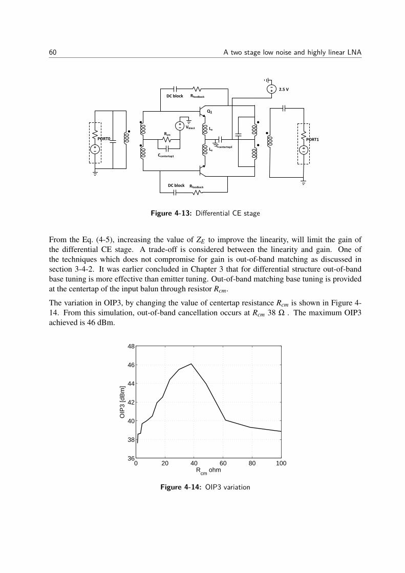
60 A two stage low noise and highly linear LNA
2.5 V
PORT1PORT0Rcm
Ccentertap1
Ccentertap2
Le
Le
Q1
Rfeedback
Rfeedback
DC block
DC block
Vbias1
Figure 4-13: Differential CE stage
From the Eq. (4-5), increasing the value of ZE to improve the linearity, will limit the gain ofthe differential CE stage. A trade-off is considered between the linearity and gain. One ofthe techniques which does not compromise for gain is out-of-band matching as discussed insection 3-4-2. It was earlier concluded in Chapter 3 that for differential structure out-of-bandbase tuning is more effective than emitter tuning. Out-of-band matching base tuning is providedat the centertap of the input balun through resistor Rcm.
The variation in OIP3, by changing the value of centertap resistance Rcm is shown in Figure 4-14. From this simulation, out-of-band cancellation occurs at Rcm 38 Ω . The maximum OIP3achieved is 46 dBm.
0 20 40 60 80 10036
38
40
42
44
46
48
Rcm
ohm
OIP
3 [d
Bm
]
Figure 4-14: OIP3 variation
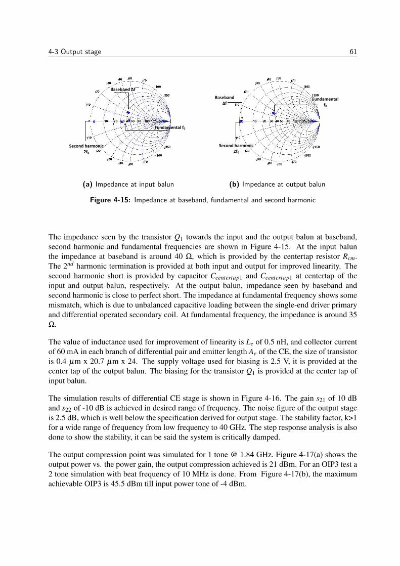
4-3 Output stage 61
Baseband Δf
Second harmonic 2f0
Fundamental f0
(a) Impedance at input balun
Baseband Δf
Second harmonic 2f0
Fundamental f0
(b) Impedance at output balun
Figure 4-15: Impedance at baseband, fundamental and second harmonic
The impedance seen by the transistor Q1 towards the input and the output balun at baseband,second harmonic and fundamental frequencies are shown in Figure 4-15. At the input balunthe impedance at baseband is around 40 Ω, which is provided by the centertap resistor Rcm.The 2nd harmonic termination is provided at both input and output for improved linearity. Thesecond harmonic short is provided by capacitor Ccentertap1 and Ccentertap1 at centertap of theinput and output balun, respectively. At the output balun, impedance seen by baseband andsecond harmonic is close to perfect short. The impedance at fundamental frequency shows somemismatch, which is due to unbalanced capacitive loading between the single-end driver primaryand differential operated secondary coil. At fundamental frequency, the impedance is around 35Ω.
The value of inductance used for improvement of linearity is Le of 0.5 nH, and collector currentof 60 mA in each branch of differential pair and emitter length Ae of the CE, the size of transistoris 0.4 µm x 20.7 µm x 24. The supply voltage used for biasing is 2.5 V, it is provided at thecenter tap of the output balun. The biasing for the transistor Q1 is provided at the center tap ofinput balun.
The simulation results of differential CE stage is shown in Figure 4-16. The gain s21 of 10 dBand s22 of -10 dB is achieved in desired range of frequency. The noise figure of the output stageis 2.5 dB, which is well below the specification derived for output stage. The stability factor, k>1for a wide range of frequency from low frequency to 40 GHz. The step response analysis is alsodone to show the stability, it can be said the system is critically damped.
The output compression point was simulated for 1 tone @ 1.84 GHz. Figure 4-17(a) shows theoutput power vs. the power gain, the output compression achieved is 21 dBm. For an OIP3 test a2 tone simulation with beat frequency of 10 MHz is done. From Figure 4-17(b), the maximumachievable OIP3 is 45.5 dBm till input power tone of -4 dBm.
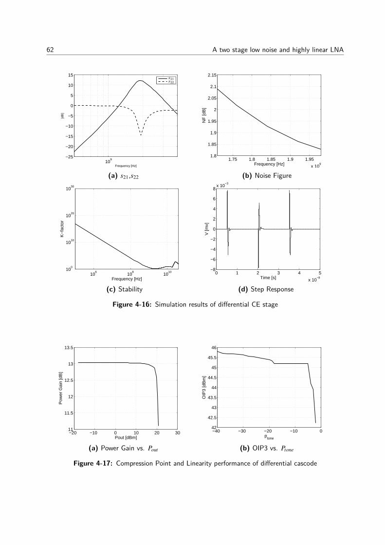
62 A two stage low noise and highly linear LNA
109
−25
−20
−15
−10
−5
0
5
10
15
Frequency [Hz]
[dB
]
s21s22
(a) s21,s22
1.75 1.8 1.85 1.9 1.95
x 109
1.8
1.85
1.9
1.95
2
2.05
2.1
2.15
Frequency [Hz]
NF
[dB
]
(b) Noise Figure
106
108
1010
100
1010
1020
1030
Frequency [Hz]
K−
fact
or
(c) Stability
0 1 2 3 4 5
x 10−8
−8
−6
−4
−2
0
2
4
6
8x 10
−3
Time [s]
V [m
v]
(d) Step Response
Figure 4-16: Simulation results of differential CE stage
−20 −10 0 10 20 3011
11.5
12
12.5
13
13.5
Pout [dBm]
Pow
er G
ain
[dB
]
(a) Power Gain vs. Pout
−40 −30 −20 −10 042
42.5
43
43.5
44
44.5
45
45.5
46
ptone
OIP
3 [d
Bm
]
(b) OIP3 vs. Ptone
Figure 4-17: Compression Point and Linearity performance of differential cascode
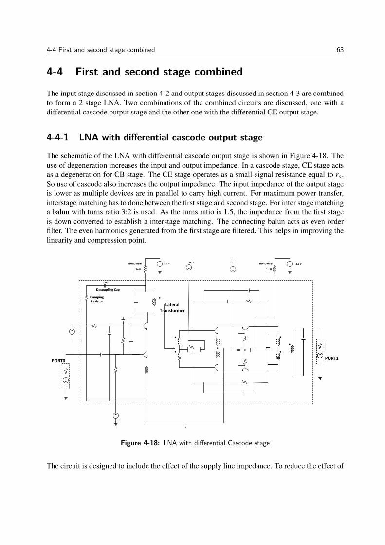
4-4 First and second stage combined 63
4-4 First and second stage combined
The input stage discussed in section 4-2 and output stages discussed in section 4-3 are combinedto form a 2 stage LNA. Two combinations of the combined circuits are discussed, one with adifferential cascode output stage and the other one with the differential CE output stage.
4-4-1 LNA with differential cascode output stage
The schematic of the LNA with differential cascode output stage is shown in Figure 4-18. Theuse of degeneration increases the input and output impedance. In a cascode stage, CE stage actsas a degeneration for CB stage. The CE stage operates as a small-signal resistance equal to ro.So use of cascode also increases the output impedance. The input impedance of the output stageis lower as multiple devices are in parallel to carry high current. For maximum power transfer,interstage matching has to done between the first stage and second stage. For inter stage matchinga balun with turns ratio 3:2 is used. As the turns ratio is 1.5, the impedance from the first stageis down converted to establish a interstage matching. The connecting balun acts as even orderfilter. The even harmonics generated from the first stage are filtered. This helps in improving thelinearity and compression point.
r
r
Lateral Transformer
PORT0PORT1
3.3 V3.3 V
1n H1n H
BondwireBondwire
Decoupling Cap
Damping Resistor
100p
Figure 4-18: LNA with differential Cascode stage
The circuit is designed to include the effect of the supply line impedance. To reduce the effect of
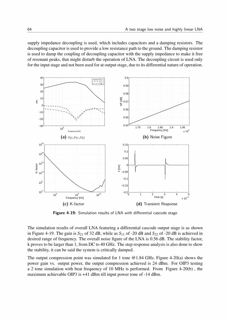
64 A two stage low noise and highly linear LNA
supply impedance decoupling is used, which includes capacitors and a damping resistors. Thedecoupling capacitor is used to provide a low resistance path to the ground. The damping resistoris used to damp the coupling of decoupling capacitor with the supply impedance to make it freeof resonant peaks, that might disturb the operation of LNA. The decoupling circuit is used onlyfor the input stage and not been used for at output stage, due to its differential nature of operation.
109
−30
−20
−10
0
10
20
30
40
Frequency [Hz]
[dB
]
s21s11s22
(a) s21,s11,s22
1.75 1.8 1.85 1.9 1.95
x 109
0.54
0.55
0.56
0.57
0.58
0.59
0.6
Frequency [Hz]
NF
[dB
]
(b) Noise Figure
106
108
1010
100
105
1010
1015
1020
1025
Frequency [Hz]
K−
fact
or
(c) K-factor
0 1 2 3 4 5
x 10−8
−0.2
−0.15
−0.1
−0.05
0
0.05
0.1
0.15
Time [s]
V [m
v]
(d) Transient Response
Figure 4-19: Simulation results of LNA with differential cascode stage
The simulation results of overall LNA featuring a differential cascode output stage is as shownin Figure 4-19. The gain is S21 of 32 dB, while as S11 of -20 dB and S22 of -20 dB is achieved indesired range of frequency. The overall noise figure of the LNA is 0.56 dB. The stability factor,k proves to be larger than 1, from DC to 40 GHz. The step response analysis is also done to showthe stability, it can be said the system is critically damped.
The output compression point was simulated for 1 tone @1.84 GHz. Figure 4-20(a) shows thepower gain vs. output power, the output compression achieved is 24 dBm. For OIP3 testinga 2 tone simulation with beat frequency of 10 MHz is performed. From Figure 4-20(b) , themaximum achievable OIP3 is +41 dBm till input power tone of -14 dBm.
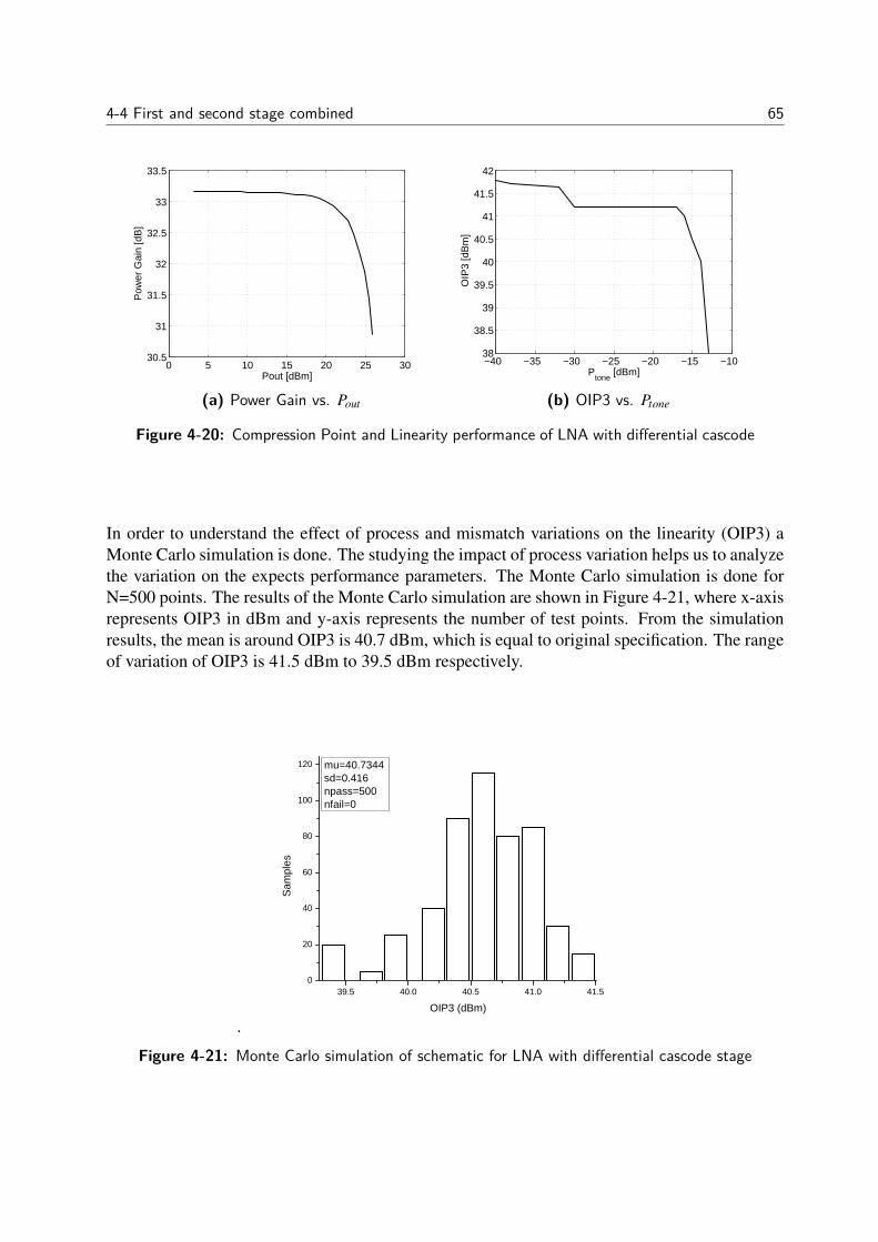
4-4 First and second stage combined 65
0 5 10 15 20 25 3030.5
31
31.5
32
32.5
33
33.5
Pow
er G
ain
[dB
]
Pout [dBm]
(a) Power Gain vs. Pout
−40 −35 −30 −25 −20 −15 −1038
38.5
39
39.5
40
40.5
41
41.5
42
Ptone
[dBm]
OIP
3 [d
Bm
]
(b) OIP3 vs. Ptone
Figure 4-20: Compression Point and Linearity performance of LNA with differential cascode
In order to understand the effect of process and mismatch variations on the linearity (OIP3) aMonte Carlo simulation is done. The studying the impact of process variation helps us to analyzethe variation on the expects performance parameters. The Monte Carlo simulation is done forN=500 points. The results of the Monte Carlo simulation are shown in Figure 4-21, where x-axisrepresents OIP3 in dBm and y-axis represents the number of test points. From the simulationresults, the mean is around OIP3 is 40.7 dBm, which is equal to original specification. The rangeof variation of OIP3 is 41.5 dBm to 39.5 dBm respectively.
.
3 9 . 5 4 0 . 0 4 0 . 5 4 1 . 0 4 1 . 50
2 0
4 0
6 0
8 0
1 0 0
1 2 0
Samp
les
O I P 3 ( d B m )
m u = 4 0 . 7 3 4 4s d = 0 . 4 1 6n p a s s = 5 0 0n f a i l = 0
Figure 4-21: Monte Carlo simulation of schematic for LNA with differential cascode stage
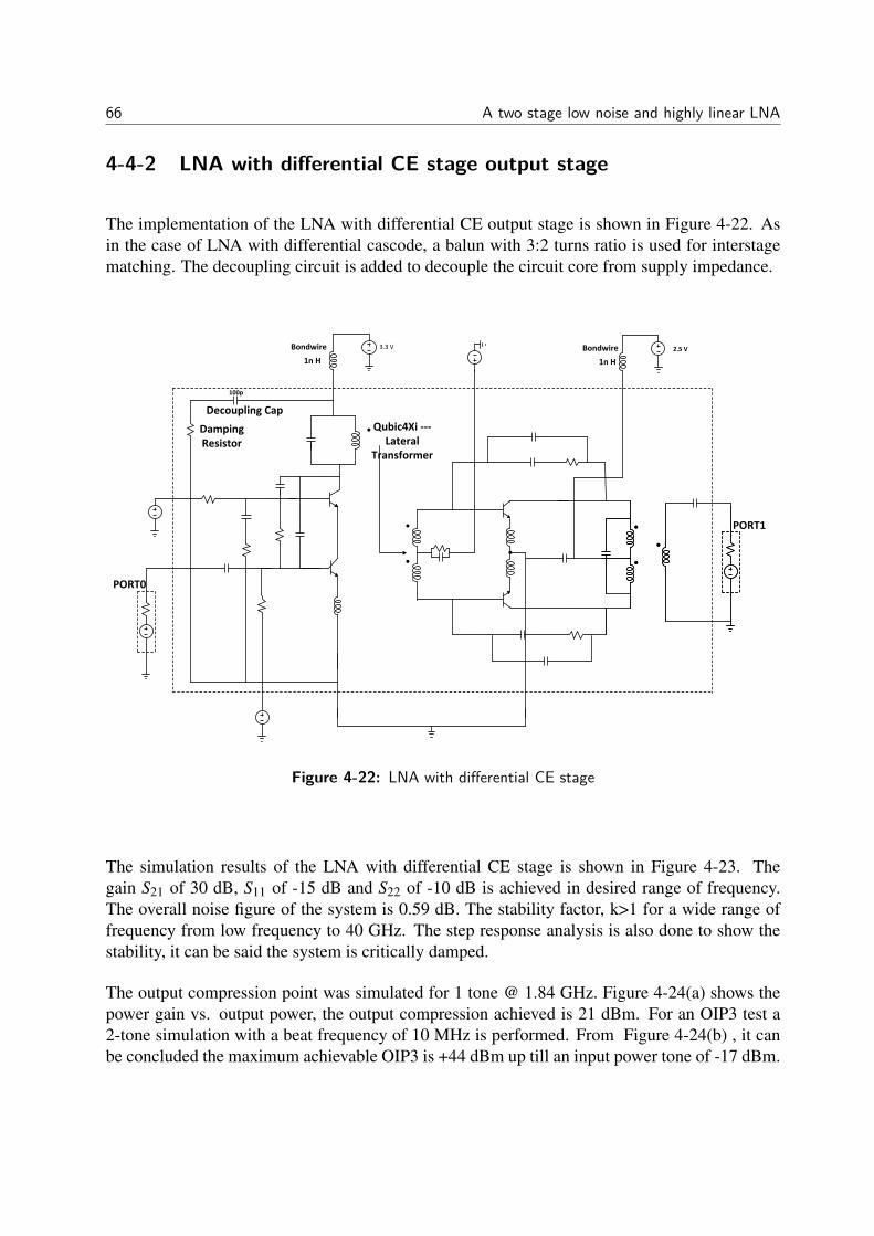
66 A two stage low noise and highly linear LNA
4-4-2 LNA with differential CE stage output stage
The implementation of the LNA with differential CE output stage is shown in Figure 4-22. Asin the case of LNA with differential cascode, a balun with 3:2 turns ratio is used for interstagematching. The decoupling circuit is added to decouple the circuit core from supply impedance.
Qubic4Xi ---Lateral
Transformer
PORT0
2.5 V3.3 V
1n H1n H
BondwireBondwire
Decoupling Cap
Damping Resistor
100p
PORT1
Figure 4-22: LNA with differential CE stage
The simulation results of the LNA with differential CE stage is shown in Figure 4-23. Thegain S21 of 30 dB, S11 of -15 dB and S22 of -10 dB is achieved in desired range of frequency.The overall noise figure of the system is 0.59 dB. The stability factor, k>1 for a wide range offrequency from low frequency to 40 GHz. The step response analysis is also done to show thestability, it can be said the system is critically damped.
The output compression point was simulated for 1 tone @ 1.84 GHz. Figure 4-24(a) shows thepower gain vs. output power, the output compression achieved is 21 dBm. For an OIP3 test a2-tone simulation with a beat frequency of 10 MHz is performed. From Figure 4-24(b) , it canbe concluded the maximum achievable OIP3 is +44 dBm up till an input power tone of -17 dBm.
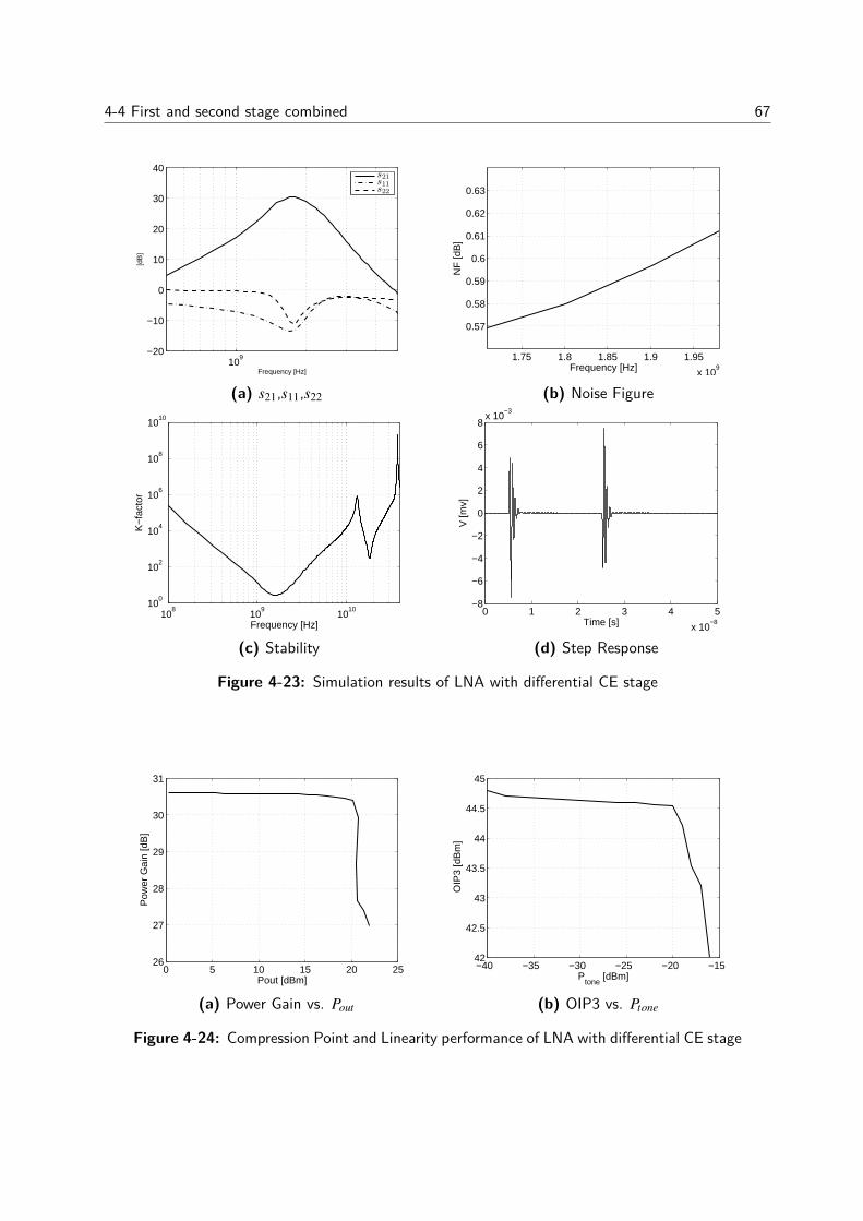
4-4 First and second stage combined 67
109
−20
−10
0
10
20
30
40
Frequency [Hz]
[dB
]
s21s11s22
(a) s21,s11,s22
1.75 1.8 1.85 1.9 1.95
x 109
0.57
0.58
0.59
0.6
0.61
0.62
0.63
Frequency [Hz]
NF
[dB
]
(b) Noise Figure
108
109
1010
100
102
104
106
108
1010
Frequency [Hz]
K−
fact
or
(c) Stability
0 1 2 3 4 5
x 10−8
−8
−6
−4
−2
0
2
4
6
8x 10
−3
Time [s]
V [m
v]
(d) Step Response
Figure 4-23: Simulation results of LNA with differential CE stage
0 5 10 15 20 2526
27
28
29
30
31
Pow
er G
ain
[dB
]
Pout [dBm]
(a) Power Gain vs. Pout
−40 −35 −30 −25 −20 −1542
42.5
43
43.5
44
44.5
45
Ptone
[dBm]
OIP
3 [d
Bm
]
(b) OIP3 vs. Ptone
Figure 4-24: Compression Point and Linearity performance of LNA with differential CE stage
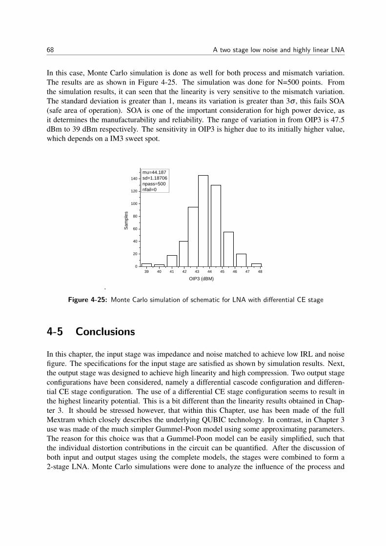
68 A two stage low noise and highly linear LNA
In this case, Monte Carlo simulation is done as well for both process and mismatch variation.The results are as shown in Figure 4-25. The simulation was done for N=500 points. Fromthe simulation results, it can seen that the linearity is very sensitive to the mismatch variation.The standard deviation is greater than 1, means its variation is greater than 3σ , this fails SOA(safe area of operation). SOA is one of the important consideration for high power device, asit determines the manufacturability and reliability. The range of variation in from OIP3 is 47.5dBm to 39 dBm respectively. The sensitivity in OIP3 is higher due to its initially higher value,which depends on a IM3 sweet spot.
.
3 9 4 0 4 1 4 2 4 3 4 4 4 5 4 6 4 7 4 80
2 0
4 0
6 0
8 0
1 0 0
1 2 0
1 4 0
Samp
les
O I P 3 ( d B M )
m u = 4 4 . 1 8 7s d = 1 . 1 8 7 0 6n p a s s = 5 0 0n f a i l = 0
Figure 4-25: Monte Carlo simulation of schematic for LNA with differential CE stage
4-5 Conclusions
In this chapter, the input stage was impedance and noise matched to achieve low IRL and noisefigure. The specifications for the input stage are satisfied as shown by simulation results. Next,the output stage was designed to achieve high linearity and high compression. Two output stageconfigurations have been considered, namely a differential cascode configuration and differen-tial CE stage configuration. The use of a differential CE stage configuration seems to result inthe highest linearity potential. This is a bit different than the linearity results obtained in Chap-ter 3. It should be stressed however, that within this Chapter, use has been made of the fullMextram which closely describes the underlying QUBIC technology. In contrast, in Chapter 3use was made of the much simpler Gummel-Poon model using some approximating parameters.The reason for this choice was that a Gummel-Poon model can be easily simplified, such thatthe individual distortion contributions in the circuit can be quantified. After the discussion ofboth input and output stages using the complete models, the stages were combined to form a2-stage LNA. Monte Carlo simulations were done to analyze the influence of the process and

4-5 Conclusions 69
device mismatch variations. This analysis indicated that, the cascode seems to be less affectedby component spread than the CE output stage, but that the CE stage seems to have the capabilityto provide the highest linearity. Simulations indicate that this is due to interactions due to theseconder terminations at the output and the feedback circuitry.

70 A two stage low noise and highly linear LNA
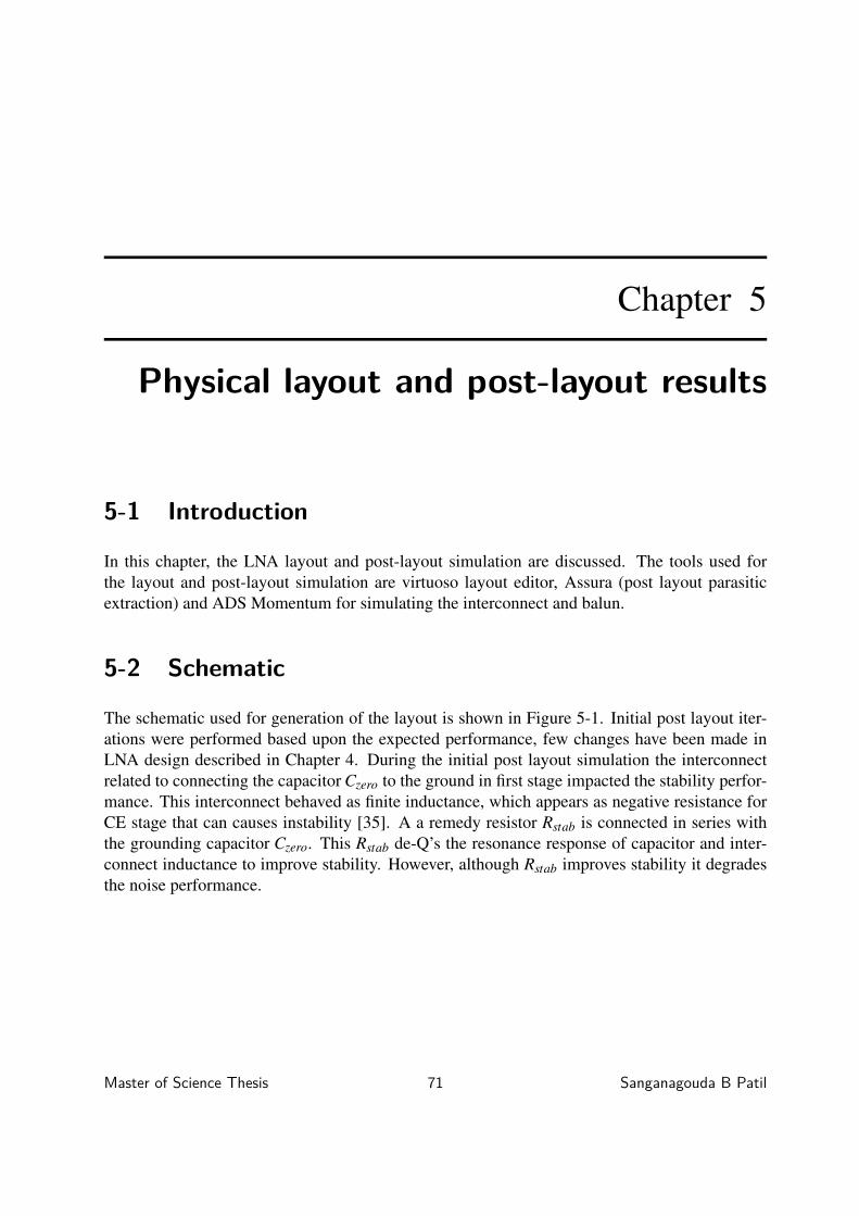
Chapter 5
Physical layout and post-layout results
5-1 Introduction
In this chapter, the LNA layout and post-layout simulation are discussed. The tools used forthe layout and post-layout simulation are virtuoso layout editor, Assura (post layout parasiticextraction) and ADS Momentum for simulating the interconnect and balun.
5-2 Schematic
The schematic used for generation of the layout is shown in Figure 5-1. Initial post layout iter-ations were performed based upon the expected performance, few changes have been made inLNA design described in Chapter 4. During the initial post layout simulation the interconnectrelated to connecting the capacitor Czero to the ground in first stage impacted the stability perfor-mance. This interconnect behaved as finite inductance, which appears as negative resistance forCE stage that can causes instability [35]. A a remedy resistor Rstab is connected in series withthe grounding capacitor Czero. This Rstab de-Q’s the resonance response of capacitor and inter-connect inductance to improve stability. However, although Rstab improves stability it degradesthe noise performance.
Master of Science Thesis 71 Sanganagouda B Patil
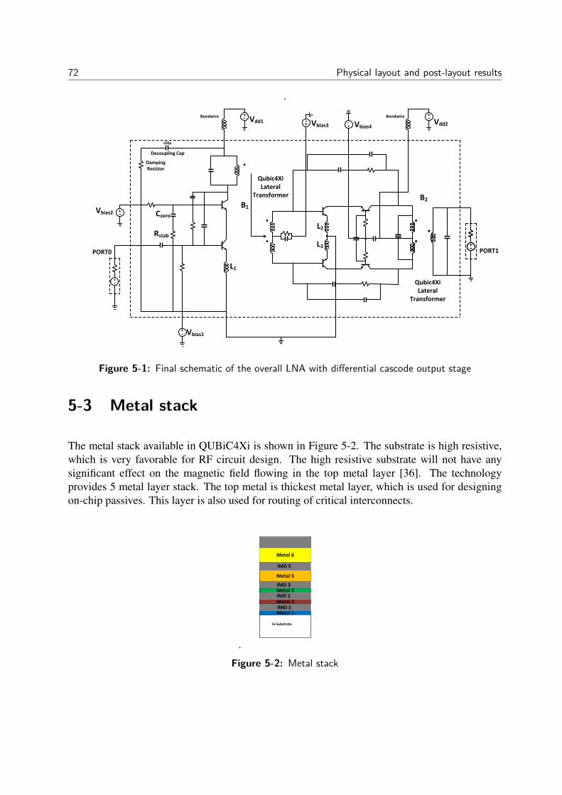
72 Physical layout and post-layout results
.
r
r
Qubic4Xi Lateral
Transformer
PORT0
BondwireBondwire
Decoupling Cap
Damping Resistor
100p
PORT1
Czero
Rstab
Vbias1
Vbias2
Vbias3 Vbias4Vdd1 Vdd2
L1
L2
L3
B1
B2
Qubic4Xi Lateral
Transformer
Figure 5-1: Final schematic of the overall LNA with differential cascode output stage
5-3 Metal stack
The metal stack available in QUBiC4Xi is shown in Figure 5-2. The substrate is high resistive,which is very favorable for RF circuit design. The high resistive substrate will not have anysignificant effect on the magnetic field flowing in the top metal layer [36]. The technologyprovides 5 metal layer stack. The top metal is thickest metal layer, which is used for designingon-chip passives. This layer is also used for routing of critical interconnects.
.
Metal 1
Metal 2
Metal 3
Metal 5
Metal 6
Si-Substrate
IMD 1
IMD 3
IMD 5
IMD 2
Figure 5-2: Metal stack
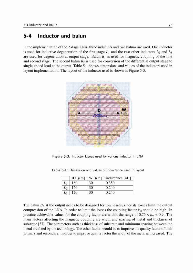
5-4 Inductor and balun 73
5-4 Inductor and balun
In the implementation of the 2 stage LNA, three inductors and two baluns are used. One inductoris used for inductive degeneration of the first stage L1 and the two other inductors L2 and L3are used for degeneration at output stage. Balun B1 is used for magnetic coupling of the firstand second stage. The second balun B2 is used for conversion of the differential output stage tosingle-ended load at the output. Table 5-1 shows dimensions and values of the inductors used inlayout implementation. The layout of the inductor used is shown in Figure 5-3.
.
ID W
Figure 5-3: Inductor layout used for various inductor in LNA
Table 5-1: Dimension and values of inductance used in layout
ID [µm] W [µm] inductance [nH]L1 180 30 0.350L2 120 30 0.240L3 120 30 0.240
The balun B2 at the output needs to be designed for low losses, since its losses limit the outputcompression of the LNA. In order to limit the losses the coupling factor km should be high. Inpractice achievable values for the coupling factor are within the range of 0.75 < km < 0.9. Themain factors affecting the magnetic coupling are width and spacing of metal and thickness ofsubstrate [37]. The parameters such as thickness of substrate and minimum spacing between themetal are fixed by the technology. The other factor, would be to improve the quality factor of bothprimary and secondary. In order to improve quality factor the width of the metal is increased. The
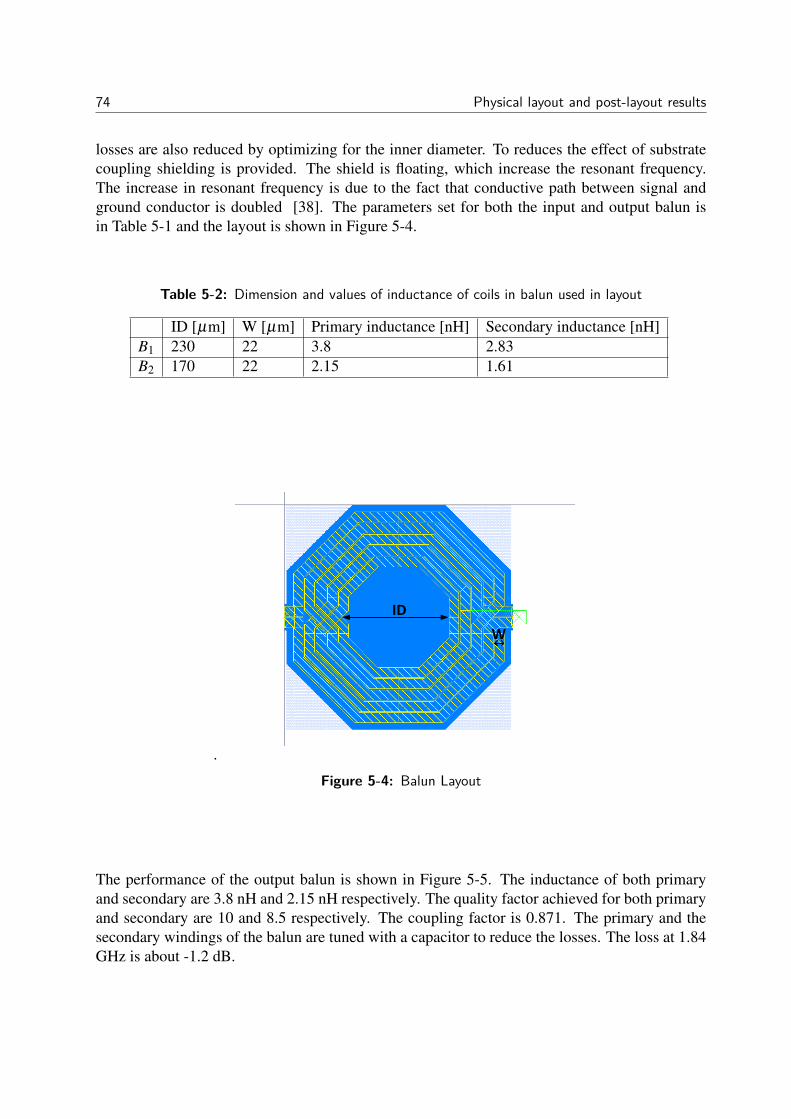
74 Physical layout and post-layout results
losses are also reduced by optimizing for the inner diameter. To reduces the effect of substratecoupling shielding is provided. The shield is floating, which increase the resonant frequency.The increase in resonant frequency is due to the fact that conductive path between signal andground conductor is doubled [38]. The parameters set for both the input and output balun isin Table 5-1 and the layout is shown in Figure 5-4.
Table 5-2: Dimension and values of inductance of coils in balun used in layout
ID [µm] W [µm] Primary inductance [nH] Secondary inductance [nH]B1 230 22 3.8 2.83B2 170 22 2.15 1.61
.
ID
W
Figure 5-4: Balun Layout
The performance of the output balun is shown in Figure 5-5. The inductance of both primaryand secondary are 3.8 nH and 2.15 nH respectively. The quality factor achieved for both primaryand secondary are 10 and 8.5 respectively. The coupling factor is 0.871. The primary and thesecondary windings of the balun are tuned with a capacitor to reduce the losses. The loss at 1.84GHz is about -1.2 dB.
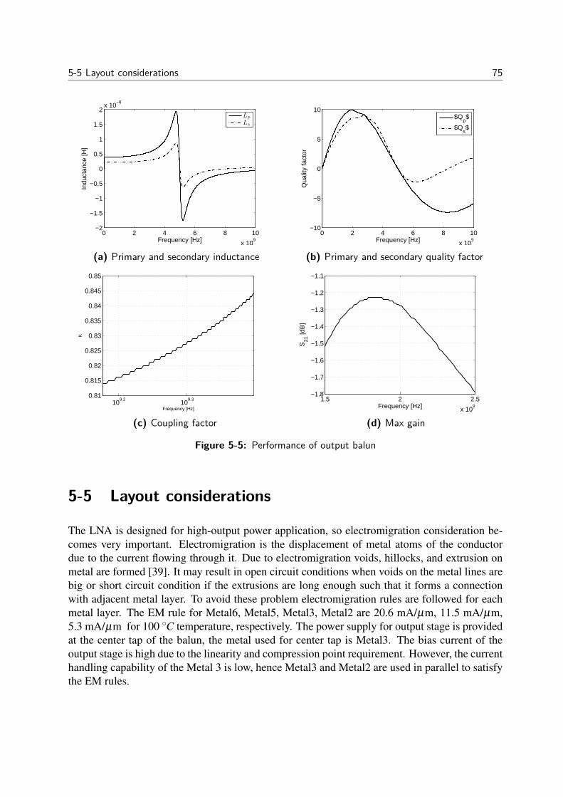
5-5 Layout considerations 75
0 2 4 6 8 10
x 109
−2
−1.5
−1
−0.5
0
0.5
1
1.5
2x 10
−8
Frequency [Hz]
Indu
ctan
ce [H
]
Lp
Ls
(a) Primary and secondary inductance
0 2 4 6 8 10
x 109
−10
−5
0
5
10
Frequency [Hz]
Qua
lity
fact
or
$Qp$
$Qs$
(b) Primary and secondary quality factor
109.2
109.3
0.81
0.815
0.82
0.825
0.83
0.835
0.84
0.845
0.85
Frequency [Hz]
K
(c) Coupling factor
1.5 2 2.5
x 109
−1.8
−1.7
−1.6
−1.5
−1.4
−1.3
−1.2
−1.1
Frequency [Hz]
S21
[dB
]
(d) Max gain
Figure 5-5: Performance of output balun
5-5 Layout considerations
The LNA is designed for high-output power application, so electromigration consideration be-comes very important. Electromigration is the displacement of metal atoms of the conductordue to the current flowing through it. Due to electromigration voids, hillocks, and extrusion onmetal are formed [39]. It may result in open circuit conditions when voids on the metal lines arebig or short circuit condition if the extrusions are long enough such that it forms a connectionwith adjacent metal layer. To avoid these problem electromigration rules are followed for eachmetal layer. The EM rule for Metal6, Metal5, Metal3, Metal2 are 20.6 mA/µm, 11.5 mA/µm,5.3 mA/µm for 100 C temperature, respectively. The power supply for output stage is providedat the center tap of the balun, the metal used for center tap is Metal3. The bias current of theoutput stage is high due to the linearity and compression point requirement. However, the currenthandling capability of the Metal 3 is low, hence Metal3 and Metal2 are used in parallel to satisfythe EM rules.
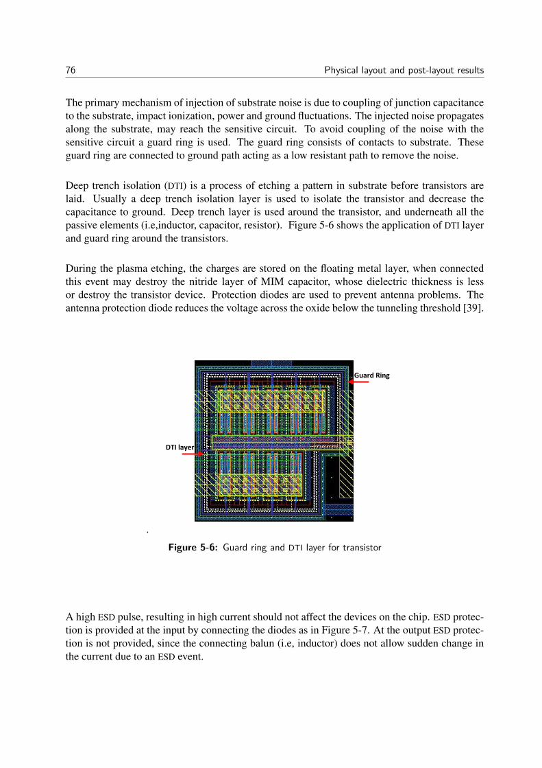
76 Physical layout and post-layout results
The primary mechanism of injection of substrate noise is due to coupling of junction capacitanceto the substrate, impact ionization, power and ground fluctuations. The injected noise propagatesalong the substrate, may reach the sensitive circuit. To avoid coupling of the noise with thesensitive circuit a guard ring is used. The guard ring consists of contacts to substrate. Theseguard ring are connected to ground path acting as a low resistant path to remove the noise.
Deep trench isolation (DTI) is a process of etching a pattern in substrate before transistors arelaid. Usually a deep trench isolation layer is used to isolate the transistor and decrease thecapacitance to ground. Deep trench layer is used around the transistor, and underneath all thepassive elements (i.e,inductor, capacitor, resistor). Figure 5-6 shows the application of DTI layerand guard ring around the transistors.
During the plasma etching, the charges are stored on the floating metal layer, when connectedthis event may destroy the nitride layer of MIM capacitor, whose dielectric thickness is lessor destroy the transistor device. Protection diodes are used to prevent antenna problems. Theantenna protection diode reduces the voltage across the oxide below the tunneling threshold [39].
.
Guard Ring
DTI layer
Figure 5-6: Guard ring and DTI layer for transistor
A high ESD pulse, resulting in high current should not affect the devices on the chip. ESD protec-tion is provided at the input by connecting the diodes as in Figure 5-7. At the output ESD protec-tion is not provided, since the connecting balun (i.e, inductor) does not allow sudden change inthe current due to an ESD event.
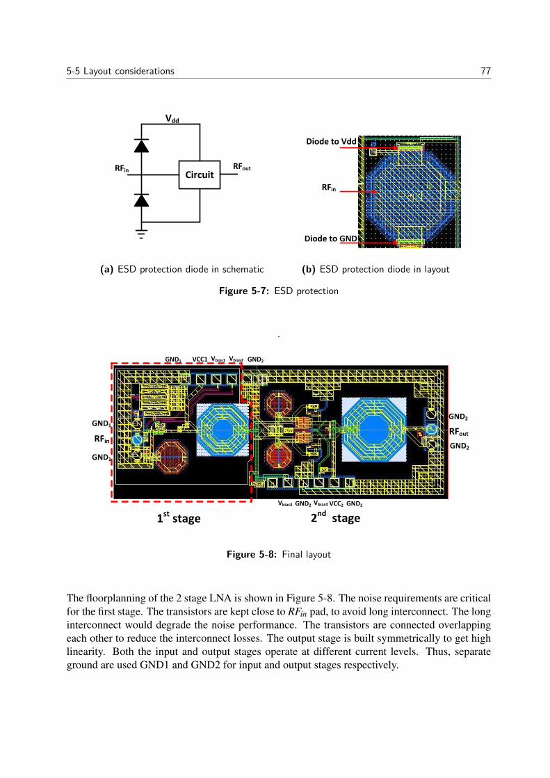
5-5 Layout considerations 77
CircuitRFin RFout
Vdd
(a) ESD protection diode in schematic
Diode to Vdd
Diode to GND
RFin
(b) ESD protection diode in layout
Figure 5-7: ESD protection
.
GND1 VCC1 Vbias1 Vbias2 GND2
RFin
GND1
GND1
GND2
GND2
RFout
GND2GND2 VCC2
1st stage 2nd stage
Vbias3 Vbias4
Figure 5-8: Final layout
The floorplanning of the 2 stage LNA is shown in Figure 5-8. The noise requirements are criticalfor the first stage. The transistors are kept close to RFin pad, to avoid long interconnect. The longinterconnect would degrade the noise performance. The transistors are connected overlappingeach other to reduce the interconnect losses. The output stage is built symmetrically to get highlinearity. Both the input and output stages operate at different current levels. Thus, separateground are used GND1 and GND2 for input and output stages respectively.
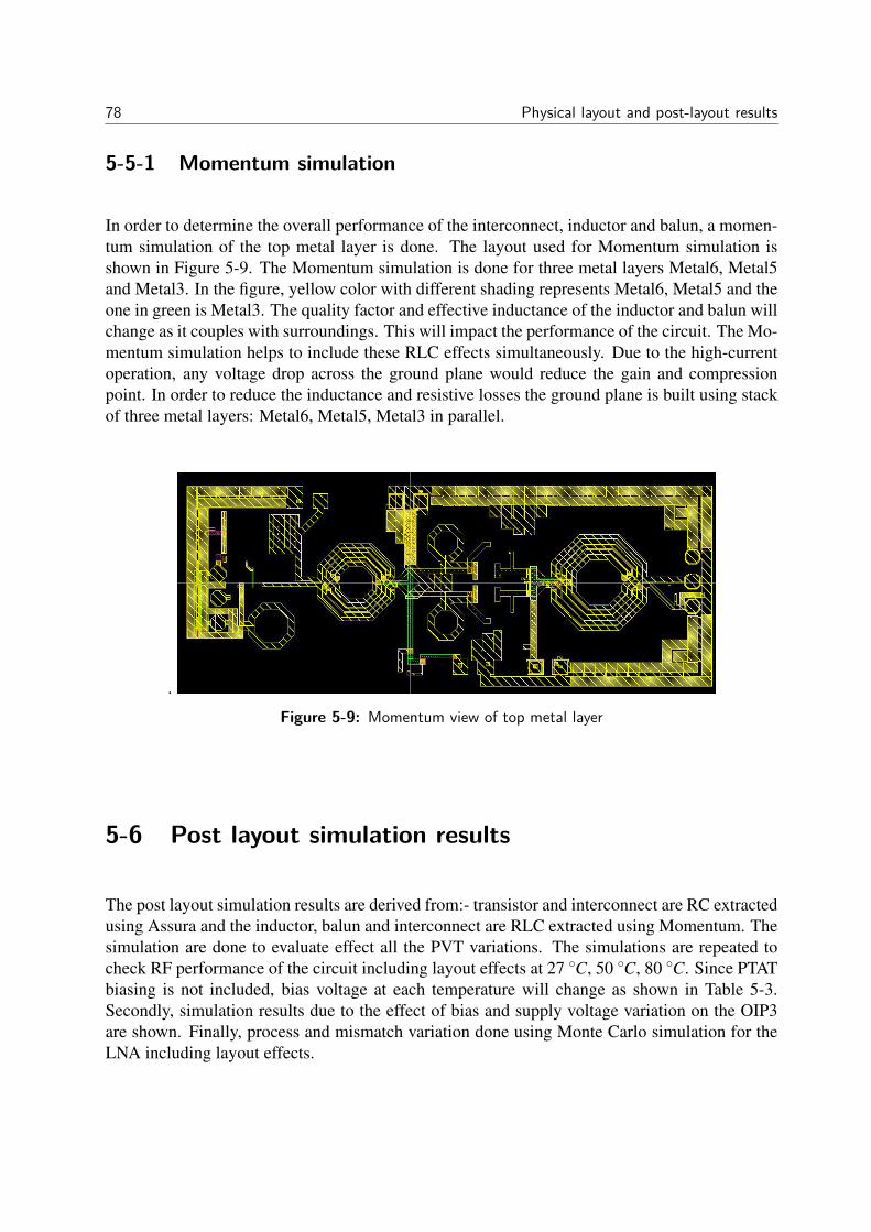
78 Physical layout and post-layout results
5-5-1 Momentum simulation
In order to determine the overall performance of the interconnect, inductor and balun, a momen-tum simulation of the top metal layer is done. The layout used for Momentum simulation isshown in Figure 5-9. The Momentum simulation is done for three metal layers Metal6, Metal5and Metal3. In the figure, yellow color with different shading represents Metal6, Metal5 and theone in green is Metal3. The quality factor and effective inductance of the inductor and balun willchange as it couples with surroundings. This will impact the performance of the circuit. The Mo-mentum simulation helps to include these RLC effects simultaneously. Due to the high-currentoperation, any voltage drop across the ground plane would reduce the gain and compressionpoint. In order to reduce the inductance and resistive losses the ground plane is built using stackof three metal layers: Metal6, Metal5, Metal3 in parallel.
.
Figure 5-9: Momentum view of top metal layer
5-6 Post layout simulation results
The post layout simulation results are derived from:- transistor and interconnect are RC extractedusing Assura and the inductor, balun and interconnect are RLC extracted using Momentum. Thesimulation are done to evaluate effect all the PVT variations. The simulations are repeated tocheck RF performance of the circuit including layout effects at 27 C, 50 C, 80 C. Since PTATbiasing is not included, bias voltage at each temperature will change as shown in Table 5-3.Secondly, simulation results due to the effect of bias and supply voltage variation on the OIP3are shown. Finally, process and mismatch variation done using Monte Carlo simulation for theLNA including layout effects.
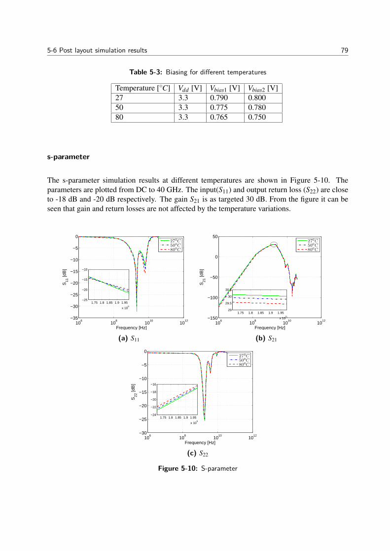
5-6 Post layout simulation results 79
Table 5-3: Biasing for different temperatures
Temperature [C] Vdd [V] Vbias1 [V] Vbias2 [V]27 3.3 0.790 0.80050 3.3 0.775 0.78080 3.3 0.765 0.750
s-parameter
The s-parameter simulation results at different temperatures are shown in Figure 5-10. Theparameters are plotted from DC to 40 GHz. The input(S11) and output return loss (S22) are closeto -18 dB and -20 dB respectively. The gain S21 is as targeted 30 dB. From the figure it can beseen that gain and return losses are not affected by the temperature variations.
106
108
1010
1012
−35
−30
−25
−20
−15
−10
−5
0
Frequency [Hz]
S11
[dB
]
270C500C800C
1.75 1.8 1.85 1.9 1.95
x 109
−25
−20
−15
−10
(a) S11
106
108
1010
1012
−150
−100
−50
0
50
Frequency [Hz]
S21
[dB
]
270C500C800C
1.75 1.8 1.85 1.9 1.95
x 109
29
29.5
30
30.5
(b) S21
106
108
1010
1012
−30
−25
−20
−15
−10
−5
0
Frequency [Hz]
S22
[dB
]
270C500C800C
1.75 1.8 1.85 1.9 1.95
x 109
−24
−22
−20
−18
−16
(c) S22
Figure 5-10: S-parameter
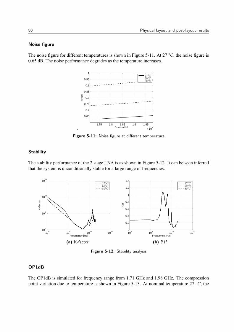
80 Physical layout and post-layout results
Noise figure
The noise figure for different temperatures is shown in Figure 5-11. At 27 C, the noise figure is0.65 dB. The noise performance degrades as the temperature increases.
.1.75 1.8 1.85 1.9 1.95
x 109
0.65
0.7
0.75
0.8
0.85
0.9
0.95
1
Frequency [Hz]
NF
[dB
]
270C500C800C
Figure 5-11: Noise figure at different temperature
Stability
The stability performance of the 2 stage LNA is as shown in Figure 5-12. It can be seen inferredthat the system is unconditionally stable for a large range of frequencies.
106
108
1010
1012
100
105
1010
1015
Frequency [Hz]
K−
fact
or
270C500C800C
(a) K-factor
106
108
1010
1012
0
0.2
0.4
0.6
0.8
1
1.2
1.4
Frequency [Hz]
B1f
270C500C800C
(b) B1f
Figure 5-12: Stability analysis
OP1dB
The OP1dB is simulated for frequency range from 1.71 GHz and 1.98 GHz. The compressionpoint variation due to temperature is shown in Figure 5-13. At nominal temperature 27 C, the
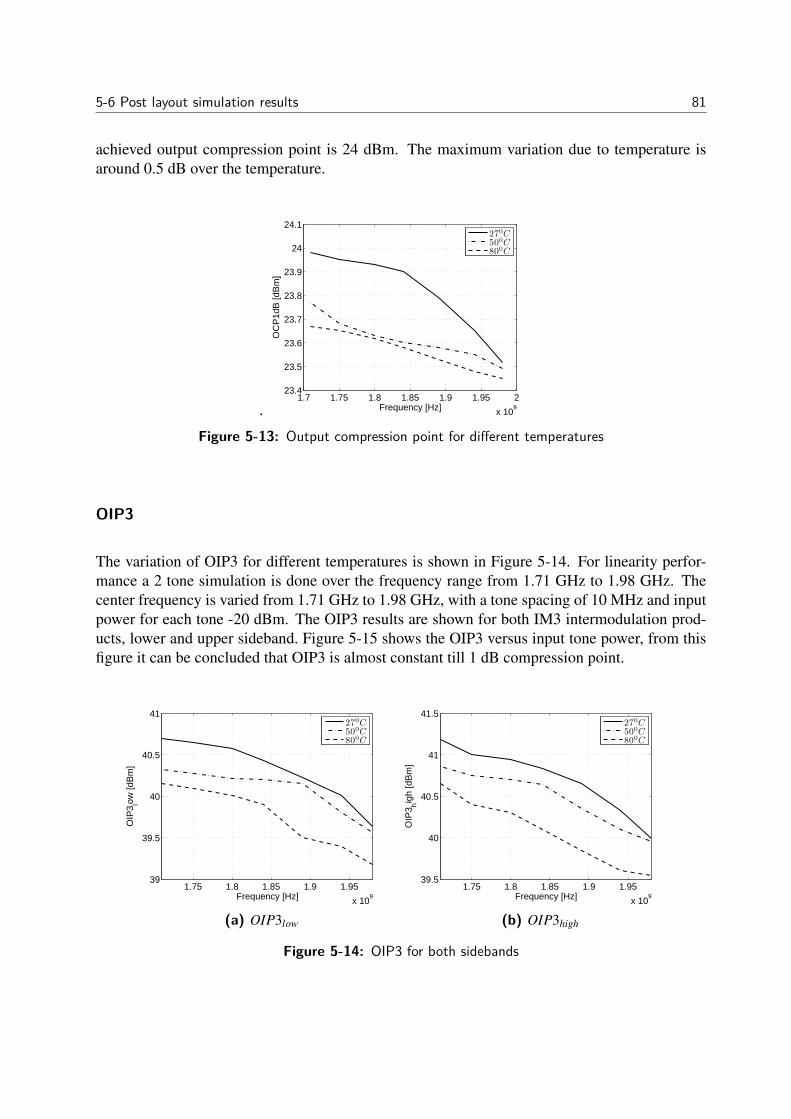
5-6 Post layout simulation results 81
achieved output compression point is 24 dBm. The maximum variation due to temperature isaround 0.5 dB over the temperature.
.1.7 1.75 1.8 1.85 1.9 1.95 2
x 109
23.4
23.5
23.6
23.7
23.8
23.9
24
24.1
Frequency [Hz]
OC
P1d
B [d
Bm
]
270C500C800C
Figure 5-13: Output compression point for different temperatures
OIP3
The variation of OIP3 for different temperatures is shown in Figure 5-14. For linearity perfor-mance a 2 tone simulation is done over the frequency range from 1.71 GHz to 1.98 GHz. Thecenter frequency is varied from 1.71 GHz to 1.98 GHz, with a tone spacing of 10 MHz and inputpower for each tone -20 dBm. The OIP3 results are shown for both IM3 intermodulation prod-ucts, lower and upper sideband. Figure 5-15 shows the OIP3 versus input tone power, from thisfigure it can be concluded that OIP3 is almost constant till 1 dB compression point.
1.75 1.8 1.85 1.9 1.95
x 109
39
39.5
40
40.5
41
Frequency [Hz]
OIP
3 low [d
Bm
]
270C500C800C
(a) OIP3low
1.75 1.8 1.85 1.9 1.95
x 109
39.5
40
40.5
41
41.5
Frequency [Hz]
OIP
3 high
[dB
m]
270C500C800C
(b) OIP3high
Figure 5-14: OIP3 for both sidebands
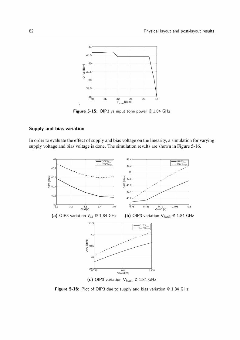
82 Physical layout and post-layout results
.−40 −35 −30 −25 −20 −1538
38.5
39
39.5
40
40.5
41
Ptone
[dBm]
OIP
3 [d
Bm
]
Figure 5-15: OIP3 vs input tone power @ 1.84 GHz
Supply and bias variation
In order to evaluate the effect of supply and bias voltage on the linearity, a simulation for varyingsupply voltage and bias voltage is done. The simulation results are shown in Figure 5-16.
3.1 3.2 3.3 3.4 3.540
40.2
40.4
40.6
40.8
41
Vdd [V]
OIP
3 [d
Bm
]
OIP3lowOIP3high
(a) OIP3 variation Vdd @ 1.84 GHz
0.78 0.785 0.79 0.795 0.840
40.2
40.4
40.6
40.8
41
41.2
41.4
Vbais1 [V]
OIP
3 [d
Bm
]
OIP3lowOIP3high
(b) OIP3 variation Vbias3 @ 1.84 GHz
0.795 0.8 0.80539.5
40
40.5
41
41.5
Vbais3 [V]
OIP
3 [d
Bm
]
OIP3lowOIP3high
(c) OIP3 variation Vbias1 @ 1.84 GHz
Figure 5-16: Plot of OIP3 due to supply and bias variation @ 1.84 GHz
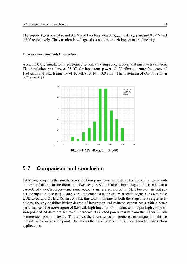
5-7 Comparison and conclusion 83
The supply Vdd is varied round 3.3 V and two bias voltage Vbias3 and Vbias1 around 0.79 V and0.8 V respectively. The variation in voltages does not have much impact on the linearity.
Process and mismatch variation
A Monte Carlo simulation is performed to verify the impact of process and mismatch variation.The simulation was done at 27 C, for input tone power of -20 dBm at center frequency of1.84 GHz and beat frequency of 10 MHz for N = 100 runs. The histogram of OIP3 is shownin Figure 5-17.
.
5.0
25.0
10.0
15.0
20.0
0.0
41.538.5 41.039.0 40.0 40.539.5
mu = 40.3385sd = 441.98mnpass = 100nfail = 0
Figure 5-17: Histogram of OIP3
5-7 Comparison and conclusion
Table 5-4, compares the simulated results form post-layout parasitic extraction of this work withthe state-of-the-art in the literature. Two designs with different input stages—a cascade and acascode of two CE stages—and same output stage are presented in [5]. However, in that pa-per the input and the output stages are implemented using different technologies 0.25 µm SiGeQUBiC4Xi and QUBiC4X. In contrast, this work implements both the stages in a single tech-nology, thereby enabling higher degree of integration and reduced system costs with a betterperformance. The noise figure of 0.65 dB, high linearity of 40 dBm, and output high compres-sion point of 24 dBm are achieved. Increased dissipated power results from the higher OP1dbcompression point achieved. This shows the effectiveness of proposed techniques to enhancelinearity and compression point. This allows the use of low cost ultra linear LNA for base stationapplications.
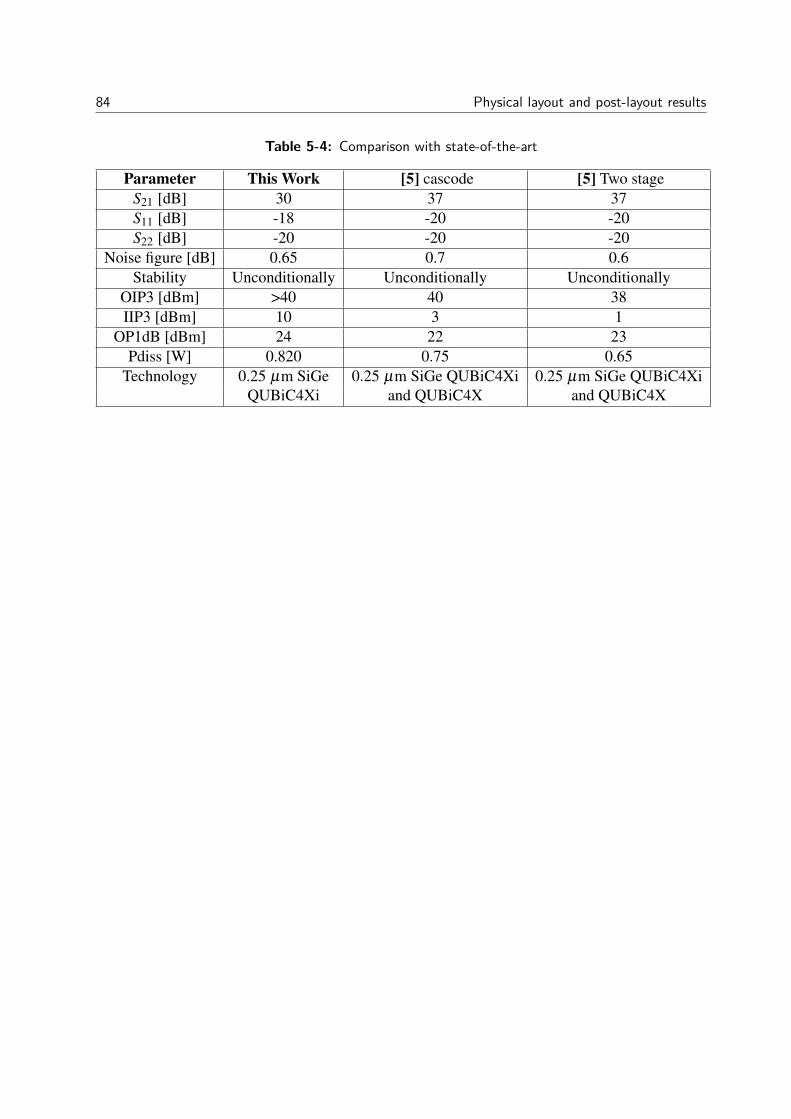
84 Physical layout and post-layout results
Table 5-4: Comparison with state-of-the-art
Parameter This Work [5] cascode [5] Two stageS21 [dB] 30 37 37S11 [dB] -18 -20 -20S22 [dB] -20 -20 -20
Noise figure [dB] 0.65 0.7 0.6Stability Unconditionally Unconditionally Unconditionally
OIP3 [dBm] >40 40 38IIP3 [dBm] 10 3 1
OP1dB [dBm] 24 22 23Pdiss [W] 0.820 0.75 0.65
Technology 0.25 µm SiGe 0.25 µm SiGe QUBiC4Xi 0.25 µm SiGe QUBiC4XiQUBiC4Xi and QUBiC4X and QUBiC4X
Chapter 6
Conclusions and future work
6-1 Conclusion
The main aim of this project was to investigate and to propose an architecture which is capableto achieve simultaneously high gain, low noise, high linearity, and high compression point usingQUBiC4Xi 0.25 µm SiGe BiCMOS technology. As such, an ultra-linear LNA for base stationwas designed, following a two stage approach. In this two-stage design, the first stage wasoptimized to achieve high gain and low noise, whereas the output stage was targeted to achievehigh linearity and high compression.
A cascode/CE-CB stage was used for the first stage, which achieves high gain (20 dB) and goodreverse isolation. The input return loss is -18 dB, which was achieved by matching using adegenerative inductor, a shunt-feedback capacitor. By optimum biasing and noise matching, anoise figure of 0.5 dB for the first stage was obtained. The linearity requirement for first stagewas satisfied using implicit IM3 cancellation.
Two differential output-stages implementations were investigated namely, a differential cascodeand a differential CE stage. The advantage of using a differential structure is that the fundamentaland the second harmonics can be controlled orthogonally, which helps in improving the linearity.Before applying any linearity improvement technique the dominant non-linearities of the transis-tor were analyzed. Techniques used to improve linearity in this report are: implicit IM3, overallnegative feedback, 2nd harmonic termination at the output and out-of-band linearization at theinput of the output stage. The implicit IM3 cancellation was done using degeneration inductor.The out-of-band cancellation was implemented as base tuning in the differential output stage.The external load is single-ended, so a balun is used at the output differential stage to convertto single-ended. A LC series resonant circuit was provided at the center tap of the transformeroutput balun to provide a 2nd harmonic trap. The maximum linearity (OIP3) achieved for thedifferential cascode and differential CE output stage are 41 dBm and 46 dBm, receptively. The
Master of Science Thesis 85 Sanganagouda B Patil
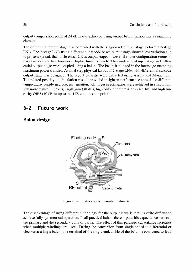
86 Conclusions and future work
output compression point of 24 dBm was achieved using output balun transformer as matchingelement.
The differential output stage was combined with the single-ended input stage to form a 2-stageLNA. The 2-stage LNA using differential cascode based output stage showed less variation dueto process spread, than differential CE as output stage, however the later configuration seems tohave the potential to achieve even higher linearity levels. The single-ended input stage and differ-ential output-stage were coupled using a balun. The balun facilitated in the interstage matchingmaximum power transfer. As final step physical layout of 2-stage LNA with differential cascodeoutput stage was designed. The layout parasitic were extracted using Assura and Momentum.The related post layout simulation results provided insight in performance spread for differenttemperature, supply and process variation. All target specification were achieved in simulation:low noise figure (0.65 dB), high gain (30 dB), high output compression (24 dBm) and high lin-earity OIP3 (40 dBm) up to the 1dB compression point.
6-2 Future work
Balun design
.
Figure 6-1: Laterally compensated balun [40]
The disadvantage of using differential topology for the output stage is that it’s quite difficult toachieve fully symmetrical operation. In all practical baluns there is parasitic capacitance betweenthe primary and the secondary coils of balun. The effect of this parasitic capacitance increaseswhen multiple windings are used. During the conversion from single-ended to differential orvice versa using a balun, one terminal of the single ended side of the balun is connected to load
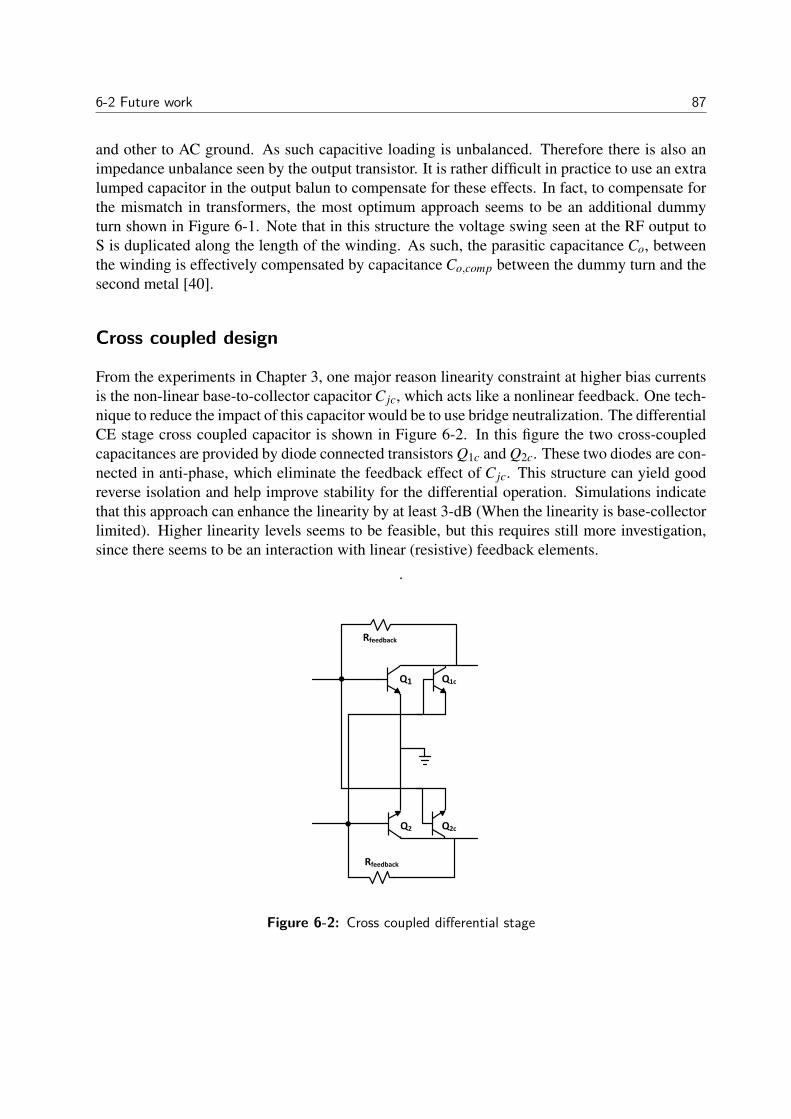
6-2 Future work 87
and other to AC ground. As such capacitive loading is unbalanced. Therefore there is also animpedance unbalance seen by the output transistor. It is rather difficult in practice to use an extralumped capacitor in the output balun to compensate for these effects. In fact, to compensate forthe mismatch in transformers, the most optimum approach seems to be an additional dummyturn shown in Figure 6-1. Note that in this structure the voltage swing seen at the RF output toS is duplicated along the length of the winding. As such, the parasitic capacitance Co, betweenthe winding is effectively compensated by capacitance Co,comp between the dummy turn and thesecond metal [40].
Cross coupled design
From the experiments in Chapter 3, one major reason linearity constraint at higher bias currentsis the non-linear base-to-collector capacitor C jc, which acts like a nonlinear feedback. One tech-nique to reduce the impact of this capacitor would be to use bridge neutralization. The differentialCE stage cross coupled capacitor is shown in Figure 6-2. In this figure the two cross-coupledcapacitances are provided by diode connected transistors Q1c and Q2c. These two diodes are con-nected in anti-phase, which eliminate the feedback effect of C jc. This structure can yield goodreverse isolation and help improve stability for the differential operation. Simulations indicatethat this approach can enhance the linearity by at least 3-dB (When the linearity is base-collectorlimited). Higher linearity levels seems to be feasible, but this requires still more investigation,since there seems to be an interaction with linear (resistive) feedback elements.
.
Q1
Rfeedback
Rfeedback
Q2 Q2c
Q1c
Figure 6-2: Cross coupled differential stage

88 Conclusions and future work
Appendix A
Appendix A
A-1 Single-ended output stage
In this appendix, the implicit IM3 cancellation and overall feedback are applied to single stageamplifier, to investigate the linearity of QUBiC4Xi technology.
A-1-1 An inductively degenerated CE stage
An inductive degenerative CE is shown in Figure A-1 (a), where Le is the degenerative inductor,Ae is emitter area and IC collector current. As discussed in section 3-3 the implicit IM3 dependson the value the of the degeneration inductor and bias current. The Figure A-1 (b) shows thevariation of OIP3 versus the degeneration inductor Le. Final simulated OIP3 may be differentbut, this plot provides a direction for optimization of the design. From figure it can be seen thatlinearity improves for increasing Le. At lower current levels the exponential distortion dominates.
Design example
When the approximate values of collector current and degenerative inductance are known, thesevalues can be used for further optimizing of the design. From the specification, the gain requiredfor second stage is 10 dB. The gain of the degenerative CE can be calculated from Eq. (A-1), butat high frequency the Miller effect needs to be considered. The Miller capacitor along with Cπ
provides a low impedance at the input for high frequencies, so the gain reduces at high frequency.
Master of Science Thesis 89 Sanganagouda B Patil
90 Appendix A
PORT1
RF_Choke
RF_Choke
DC_Block
DC_Block
PORT0
50Ω
50Ω
Le
Ae
IC
(a) Inductively degenerated CE stage
0 0.5 1 1.5 2 2.5 324
25
26
27
28
29
30
31
Le [nH]
OIP
3 [d
Bm
]
(b) OIP3 vs. Le @ 1.84 GHz of the size:0.4µm x 20.7 µm x 25 QUBiC4Xi SiGe BNAtransistor
Figure A-1
The transconductance required to achieve high gain depends on the collector current (gm = ICVT
).For sustaining high collector current the emitter length needs to be chosen to be larger. A tran-sistor size of 0.4 µm x 20.7 µm x 25 is considered for design. For this size of device C je value is5.824 pF. The optimum value of inductor required to improve the linearity is given by Eq. (A-2).By substituting the value of C je and operating frequency of 1.84 GHz, the value of the inductorrequired is 1.4 nH. The value of load impedance required to achieve the required gain is cal-culated. The biasing network are optimized for out of band IM3 cancellation to improve thelinearity further. The supply voltage used is 2.5 V and collector current is 51 mA. The OIP3versus input power tone is as shown in Figure A-2. The results obtained by this architecture isgiven by the table A-1.
Av =−gm ∗[email protected]
1+gm ∗Ze(A-1)
Le,opt =50
C jeω2t
(A-2)
A-1 Single-ended output stage 91
.−40 −35 −30 −25 −20 −15 −10 −5 030
30.5
31
31.5
32
32.5
33
Ptone [mA]
OIP
3 [d
Bm
]
Figure A-2: OIP3 Vs Input Power
Table A-1: Design matrix achieved for an inductively degenerated CE stage
Parameter ValueGain [email protected] Hz [dB] 10OCP1 [dBm] 18.53ICP1 [dBm] 8.53OIP3 [dBm] 32.5Stability unconditionally stable
The gain requirement can be easily achieved with the CE stage, but it is limited for its OIP3.The main limiting factor for inductive degenerated CE stage in achieving high linearity is base-collector capacitance and base-charge modulation. A cascode stage can be used to reduce thefeedback of base collector capacitor.
A-1-2 An inductively degenerated cascode
The configuration of an inductive degenerative cascode is shown in Figure A-3, where Q1 isCE stage, Q2 is CB stage, Le is degenerative inductor, Ae is the emitter area and, IC collec-tor current. Figure A-4 at lower current levels the linearity is improved using to implicit IM3cancellation through degeneration inductor.
92 Appendix A
.
PORT1
RF_Choke
RF_Choke
DC_Block
DC_Block
PORT0
AC_Grounding
30 pF
50Ω
50Ω Le
Ae
IC
Q2
Q1
Figure A-3: Cascode inductive degeneration
.0 0.5 1 1.5 2
22
24
26
28
30
32
34
36
Le [nH]
OIP
3 [d
Bm
]
Figure A-4: OIP3 vs. Le @ 1.84 GHz of the size:0.4 µm x 20.7 µm x 25 QUBiC4Xi SiGeBNA transistor
Design example
A-1 Single-ended output stage 93
From Figure A-4 the optimum value for degenerative inductor is obtained. The supply voltagerequired for the biasing of cascode stage is 3.3 V. The collector to base voltage VCB is kept low toreduce the non-linearities introduced by base to collector capacitor of CE stage (≈10 mV). TheOIP3 versus the input power tone is plotted as shown in Figure A-5. The achieved specificationfrom inductive degenerated cascode is as given by table A-2.
.−40 −35 −30 −25 −20 −15 −10 −533
33.5
34
34.5
35
35.5
Ptone [mA]
OIP
3 [d
Bm
]
Figure A-5: OIP3 Vs Input Power
Table A-2: Design Matrix of an inductively degenerated cascode
Parameter ValueGain [email protected] Hz [dB] 22OCP1 [dBm] 19.5ICP1 [dBm] -2.5OIP3 [dBm] 35Stability unconditionally stable
From the design, it can be concluded that the even after using a cascode configuration requiredspecification of linearity (OIP3)are not achieved. The advantage of using cascode is high loopgain. The gain achieved from cascode is 22 dB which is high when compared to the specificationof the output stage. This high gain can be reduced by using a negative feedback. An inductivedegenerative feedback cascode with feedback is discussed in next section.
A-1-3 An inductive degenerated cascode with feedback
An inductive degenerated cascode with feedback is shown in Figure A-6. The feedback is appliedthrough resistor R f eedback. Due to overall feedback the linearity is improved, which is shown in
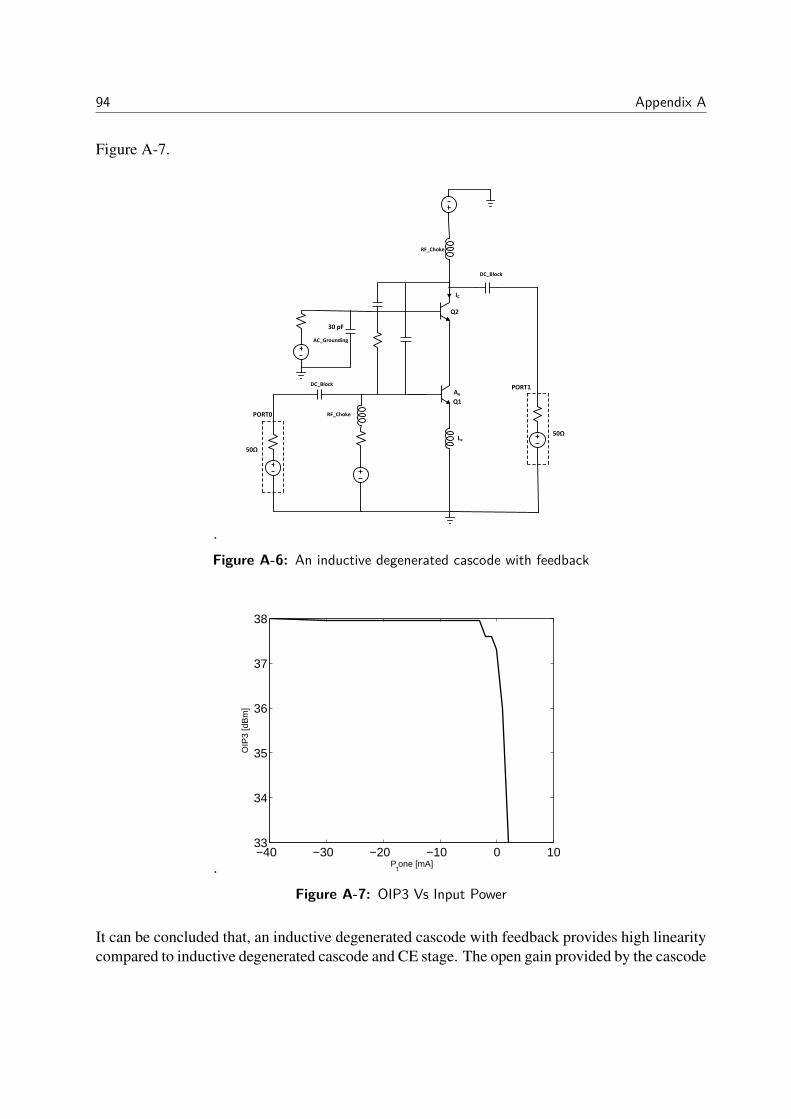
94 Appendix A
Figure A-7.
.
PORT1
RF_Choke
RF_Choke
DC_Block
DC_Block
PORT0
AC_Grounding
30 pF
50Ω
50Ω Le
Ae
IC
Q2
Q1
Figure A-6: An inductive degenerated cascode with feedback
.−40 −30 −20 −10 0 1033
34
35
36
37
38
Ptone [mA]
OIP
3 [d
Bm
]
Figure A-7: OIP3 Vs Input Power
It can be concluded that, an inductive degenerated cascode with feedback provides high linearitycompared to inductive degenerated cascode and CE stage. The open gain provided by the cascode
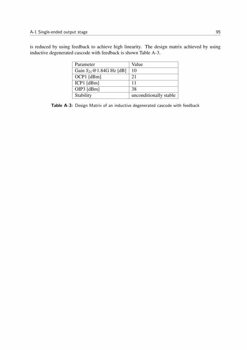
A-1 Single-ended output stage 95
is reduced by using feedback to achieve high linearity. The design matrix achieved by usinginductive degenerated cascode with feedback is shown Table A-3.
Parameter ValueGain [email protected] Hz [dB] 10OCP1 [dBm] 21ICP1 [dBm] 11OIP3 [dBm] 38Stability unconditionally stable
Table A-3: Design Matrix of an inductive degenerated cascode with feedback

96 Appendix A
Bibliography
[1] A. Goldsmith, Wireless Communications. Cambridge University Press, 2005.
[2] C.-L. Lim, “Integrated LNA Serves Base Station Needs,” tech. rep., Avago Technologies,09 2011.
[3] S. Motoroiu, “Multi-band/Multi-Mode RF Front-end Receiver for Basestation Applications.” TU Delft library repository, August 2011.
[4] D. L. Gabriele Manganaro, Advances in Analog and RF IC Design for Wireless Communi-cation Systems. Elsevier, 2013.
[5] J. Bergervoet, D. Leenaerts, G. de Jong, E. van der Heijden, J. W. Lobeek, and A. Simin,“A 1.95 GHz Sub-1 dB NF, +40 dBm OIP3 WCDMA LNA Module,” Solid-State Circuits,IEEE Journal of, vol. 47, no. 7, pp. 1672–1680, 2012.
[6] J. Yuan, SiGe, GaAs, and InP heterojunction biopolar transistors. Wiley, 1999.
[7] F. Ali and A. Gupta, HEMTs and HBTs: devices, fabrication, and circuits. Artech Housemicrowave library, Artech House, 1991.
[8] MGA-13316, “High Gain, High Linearity Low Noise Amplifier,” 12 2011.
[9] MML20242H, “Enhancement Mode pHEMT Technology EpHEMT Low noise amlifier,” 42013.
[10] SKY65040-360LF, “Low Noise Amplifier1.5 2.4 GHz ,” 3 2009.
[11] BGU7063, “Analog controlled high linearity low noise variable gain amplifier,” 12 2012.
[12] E. Johnson, “Physical limitations on frequency and power parameters of transistors,” in IREInternational Convention Record, vol. 13, pp. 27–34, 1965.
Master of Science Thesis 97 Sanganagouda B Patil
98 Bibliography
[13] D. Terlep, “Receiver Sensitivity Equation for Spread Spectrum Systemss,” tech. rep.,Maxim Integarted, 06 2002.
[14] A. Richardson, WCDMA Design Handbook. Cambridge University Press, 2005.
[15] G. TS, “3rd Generation Partnership Project; Technical Specification Group Radio AccessNetwork; Base Station (BS) radio transmission and reception (FDD).”
[16] L. de Vreede, “Bipolar / CMOS RF Devices.” Chapter 2, ET4294 Microwave Circuit De-sign, 2011.
[17] M. van der Heijden, RF Amplifier Design Techniques for Linearity and Dynamic Range.PhD thesis, Delft university of technology, may 2005.
[18] P. Wambacq and W. Sansen, Distortion Analysis of Analog Integrated Circuits. TheSpringer International Series in Engineering and Computer Science, Springer, 1998.
[19] G. Gonzlez, Microwave transistor amplifiers: analysis and design. Prentice Hall, 1997.
[20] C. Verhoeven and G. Monna, Structured Electronic Design: Negative-Feedback Amplifiers.Springer, 2003.
[21] J. Long, “Monolithic transformers for silicon RF IC design,” Solid-State Circuits, IEEEJournal of, vol. 35, no. 9, pp. 1368–1382, 2000.
[22] K. T. Ng, B. Rejaei, and J. Burghartz, “Substrate effects in monolithic RF transformers onsilicon,” Microwave Theory and Techniques, IEEE Transactions on, vol. 50, no. 1, pp. 377–383, 2002.
[23] J. Rogers and C. Plett, Radio Frequency Integrated Circuit Design. Artech House mi-crowave library, Artech House, 2003.
[24] L. de Vreede, HF silicon ICs for wideband communication systems. PhD thesis, Delftuniversity of technology, June 1996.
[25] M. van der Heijden, L. de Vreede, and J. Burghartz, “On the design of unilateral dual-loop feedback low-noise amplifiers with simultaneous noise, impedance, and IIP3 match,”Solid-State Circuits, IEEE Journal of, vol. 39, no. 10, pp. 1727–1736, 2004.
[26] K. L. Fong and R. Meyer, “High-frequency nonlinearity analysis of common-emitter anddifferential-pair transconductance stages,” Solid-State Circuits, IEEE Journal of, vol. 33,no. 4, pp. 548–555, 1998.
[27] L. de Vreede, “Low Noise Techniques.” Chapter 3, ET4294 Microwave Circuit Design,2011.
[28] L. de Vreede, “ Large Signal Operation.” Chapter 4, ET4294 Microwave Circuit Design,2011.
99
[29] M. Spirito, L. de Vreede, L. Nanver, S. Weber, and J. Burghartz, “Power amplifier PAE andruggedness optimization by second-harmonic control,” Solid-State Circuits, IEEE Journalof, vol. 38, no. 9, pp. 1575–1583, 2003.
[30] K. Buisman, Device Realization,Characterization and Modeling for Linear RF Applica-tions. PhD thesis, Delft university of technology, November 2011.
[31] B. Razavi, RF Microelectronics. Prentice Hall International Series in the Physical andChemical Engineering Sciences, Pearson Education, 2011.
[32] B. Kang, J. Yu, H. Shin, S. Ko, W. Ko, S.-G. Yang, W. Choo, and B.-H. Park, “Design andAnalysis of a Cascode Bipolar Low-Noise Amplifier With Capacitive Shunt Feedback Un-der Power-Constraint,” Microwave Theory and Techniques, IEEE Transactions on, vol. 59,no. 6, pp. 1539–1551, 2011.
[33] D. Leenaerts, J. Bergervoet, J. W. Lobeek, and M. Schmidt-Szalowski,“900MHz/1800MHz GSM base station LNA with sub-1dB noise figure and +36dBmOIP3,” in Radio Frequency Integrated Circuits Symposium (RFIC), 2010 IEEE, pp. 513–516, 2010.
[34] S. Voinigescu, M. Maliepaard, J. Showell, G. Babcock, D. Marchesan, M. Schroter,P. Schvan, and D. Harame, “A scalable high-frequency noise model for bipolar transistorswith application to optimal transistor sizing for low-noise amplifier design,” Solid-StateCircuits, IEEE Journal of, vol. 32, no. 9, pp. 1430–1439, 1997.
[35] J. R. Long, “Small-signal RF and MMIC Amplifier.” ET4254, RF Integrated circuit design,2012.
[36] J. R. Long, “Passive components and RFIC design.” ET4254, RF Integrated circuit design,2012.
[37] H. Greenhouse, “Design of Planar Rectangular Microelectronic Inductors,” Parts, Hybrids,and Packaging, IEEE Transactions on, vol. 10, no. 2, pp. 101–109, 1974.
[38] T. Cheung and J. Long, “Shielded passive devices for silicon-based monolithic microwaveand millimeter-wave integrated circuits,” Solid-State Circuits, IEEE Journal of, vol. 41,no. 5, pp. 1183–1200, 2006.
[39] “QUBiC4 PlatformDesign Manual,” tech. rep., NXP semiconductor, 12 2012.
[40] Y. Zhao and J. Long, “A Wideband, Dual-Path, Millimeter-Wave Power Amplifier With 20dBm Output Power and PAE Above 15% in 130 nm SiGe-BiCMOS,” Solid-State Circuits,IEEE Journal of, vol. 47, no. 9, pp. 1981–1997, 2012.

100 Bibliography

Glossary
List of Acronyms
IRL Low return loss
ORL Output return loss
LNA Low noise amplifier
HEMT High electron mobility transistor
HBT Heterjunction bipolar transistor
GaAs Gallium arsenide
InP Indium phosphide
SiGe Silicon germanium
BJT Bipolar junction transistor
NF Noise figure
IF Intermediate frequency
pHEMT Pseudomorphic High electron mobility transistor
MESFET MetalâASsemiconductor field effect transistor
IM3 3rd order intermodulation component
IIP3 Input third order intercept
OIP3 Output third order intercept
Master of Science Thesis 101 Sanganagouda B Patil
102 Glossary
FDD Frequency division duplex
GSM Global system for mobile communications
CE Common emitter
CB Common base
HV High voltage
NF Noise figure
IF Intermediate frequency
DCS Digital Cellular System
ESD Electrostatic discharge
DTI Deep trench isolation
ADS Advanced Design System