Embed Size (px)
Citation preview
Materials, Devices, and Circuit Architectures for Future Electronics
Thomas N. Theis
Department of Electrical Engineering
Columbia University
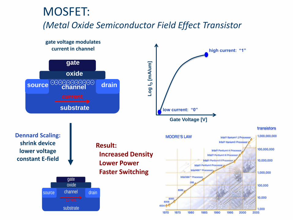
MOSFET: (Metal Oxide Semiconductor Field Effect Transistor
current
substrate
source drain
oxide
gate
channel
gate voltage modulates current in channel
current
substrate
source drain
oxide gate
channel
Lo
g I
D[m
A/u
m]
Gate Voltage [V]
low current: “0”
Dennard Scaling:shrink devicelower voltage
constant E-field
Result:Increased DensityLower PowerFaster Switching
high current: “1”
- - - - - - - - - - -
3
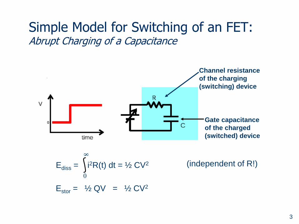
Simple Model for Switching of an FET:Abrupt Charging of a Capacitance
Ediss = i2R(t) dt = ½ CV2
0
8
Estor = ½ QV = ½ CV2
(independent of R!)
Channel resistance
of the charging
(switching) device
Gate capacitance
of the charged
(switched) device

4
Adiabatic SwitchingThe stored energy need not be dissipated
( T >> RC)
Topics
Post-CMOS Device Research – the Need and the Vast Opportunity
Growing Research Investment
Two Broad Classes of Emerging Devices
“Steep Slope” Devices (TFETs and More)
Nanomagnetic Devices (Spintronics)
Device Performance Benchmarking:Comparing and Evaluating Emerging Devices
Conclusion: Devices and Architectures –the Unexplored Research Landscape
5
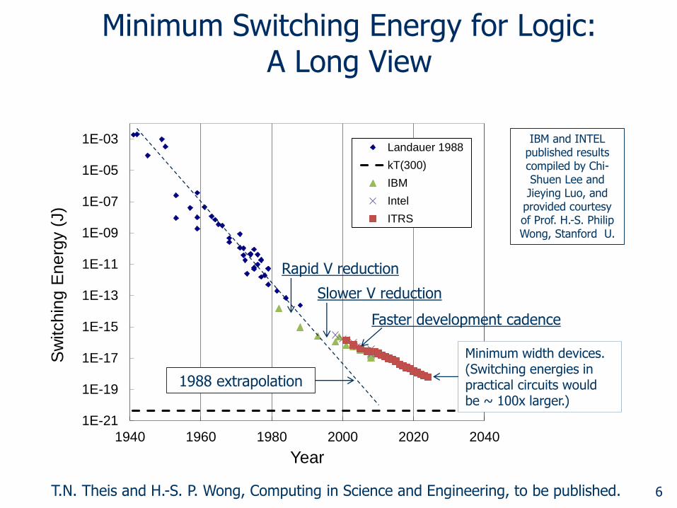
Minimum Switching Energy for Logic: A Long View
6
IBM and INTEL published results compiled by Chi-Shuen Lee and Jieying Luo, and
provided courtesy of Prof. H.-S. Philip Wong, Stanford U.
1E-21
1E-19
1E-17
1E-15
1E-13
1E-11
1E-09
1E-07
1E-05
1E-03
1940 1960 1980 2000 2020 2040
Sw
itchin
g E
nerg
y (
J)
Year
Chart Title
Landauer 1988
kT(300)
IBM
Intel
ITRS
1988 extrapolation
Rapid V reduction
Slower V reduction
Faster development cadence
Minimum width devices.(Switching energies in practical circuits would be ~ 100x larger.)
T.N. Theis and H.-S. P. Wong, Computing in Science and Engineering, to be published.
7
0.01
0.1
1
0.01
0.1
1
10
100
1990 1995 2000 2005 2010 2015 2020
CG
P/M
1 P
itch
(m
m)
SR
AM
Are
a(m
m2)
Year
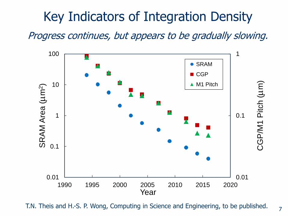
SRAM
CGP
M1 Pitch
Key Indicators of Integration Density
Progress continues, but appears to be gradually slowing.
T.N. Theis and H.-S. P. Wong, Computing in Science and Engineering, to be published.
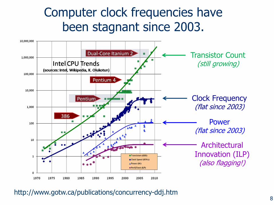
Computer clock frequencies have been stagnant since 2003.
8http://www.gotw.ca/publications/concurrency-ddj.htm
Clock Frequency(flat since 2003)
Transistor Count(still growing)
Architectural Innovation (ILP)
(also flagging!)
Power(flat since 2003)
En
erg
y
9
Log Current
Voltage
Sub-thresholdSlope
Ion
Ioff
Vdd0
distance
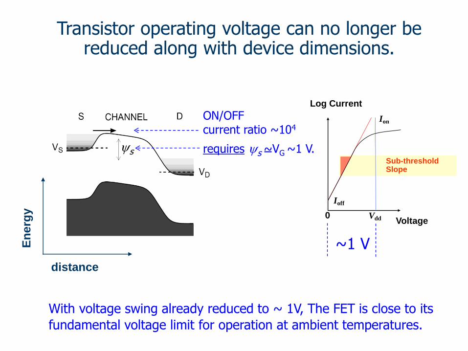
With voltage swing already reduced to ~ 1V, The FET is close to its
fundamental voltage limit for operation at ambient temperatures.
Transistor operating voltage can no longer be reduced along with device dimensions.
~1 V
ys
ON/OFF current ratio ~104
requires ys ~VG ~1 V.
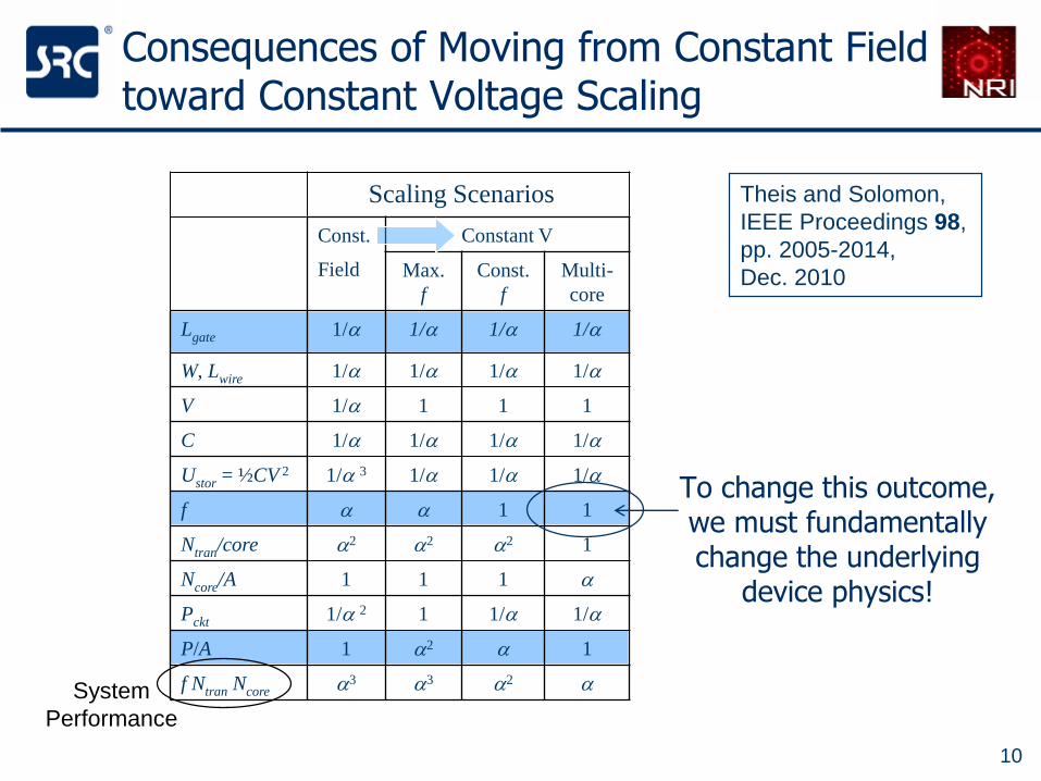
Consequences of Moving from Constant Field toward Constant Voltage Scaling
Scaling Scenarios
Const.
Field
Constant V
Max.
f
Const.
f
Multi-
core
Lgate 1/a 1/a 1/a 1/a
W, Lwire 1/a 1/a 1/a 1/a
V 1/a 1 1 1
C 1/a 1/a 1/a 1/a
Ustor = ½CV 2 1/a 3 1/a 1/a 1/a
f a a 1 1
Ntran/core a2 a2 a2 1
Ncore/A 1 1 1 a
Pckt 1/a 2 1 1/a 1/a
P/A 1 a2 a 1
f Ntran Ncore a3 a3 a2 a
10
Theis and Solomon,
IEEE Proceedings 98,
pp. 2005-2014,
Dec. 2010
To change this outcome, we must fundamentally change the underlying
device physics!
System
Performance
Briefly summarizing the last 10 years…
To keep areal power density and total power within economically acceptable limits, industry froze clock speed and slowed the deployment of multiple cores.(See the simple constant voltage scaling argument by T.N. Theis and P.M. Solomon, “In Quest of the ‘Next Switch’: Prospects for Greatly Reduced Power Dissipation in a Successor to the Silicon Field-Effect Transistor,” IEEE Proc. 98, 2005–2014, Dec. 2010.)
To escape this new status quo, we’ve begun to explore devices with switching mechanisms that are fundamentally different from that of the conventional FET, and architectures than are fundamentally different from the von Neumann architecture.
11

The Unexplored Research Landscape
12
1E-21
1E-19
1E-17
1E-15
1E-13
1E-11
1E-09
1E-07
1E-05
1E-03
1940 1960 1980 2000 2020 2040
Sw
itchin
g E
nerg
y (
J)
Year
Chart Title
Landauer 1988
ITRS
IBM
Intel
kT(300)
Rough limit for abrupt switching (i.e. nearly all current device research) set by tolerable error rate due to thermal upsets.
NO lower limit for adiabatic switching in energy-conserving circuits.
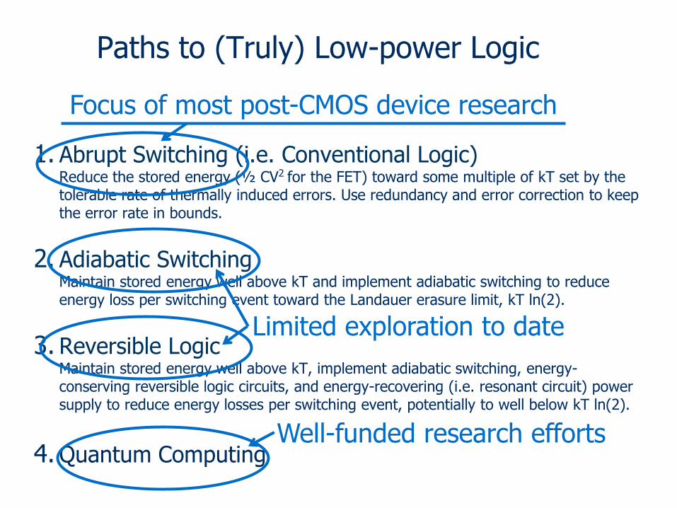
Paths to (Truly) Low-power Logic
1. Abrupt Switching (i.e. Conventional Logic)Reduce the stored energy (½ CV2 for the FET) toward some multiple of kT set by the tolerable rate of thermally induced errors. Use redundancy and error correction to keep the error rate in bounds.
2. Adiabatic SwitchingMaintain stored energy well above kT and implement adiabatic switching to reduce energy loss per switching event toward the Landauer erasure limit, kT ln(2).
3. Reversible LogicMaintain stored energy well above kT, implement adiabatic switching, energy-conserving reversible logic circuits, and energy-recovering (i.e. resonant circuit) power supply to reduce energy losses per switching event, potentially to well below kT ln(2).
4. Quantum Computing
Focus of most post-CMOS device research
Limited exploration to date
Well-funded research efforts
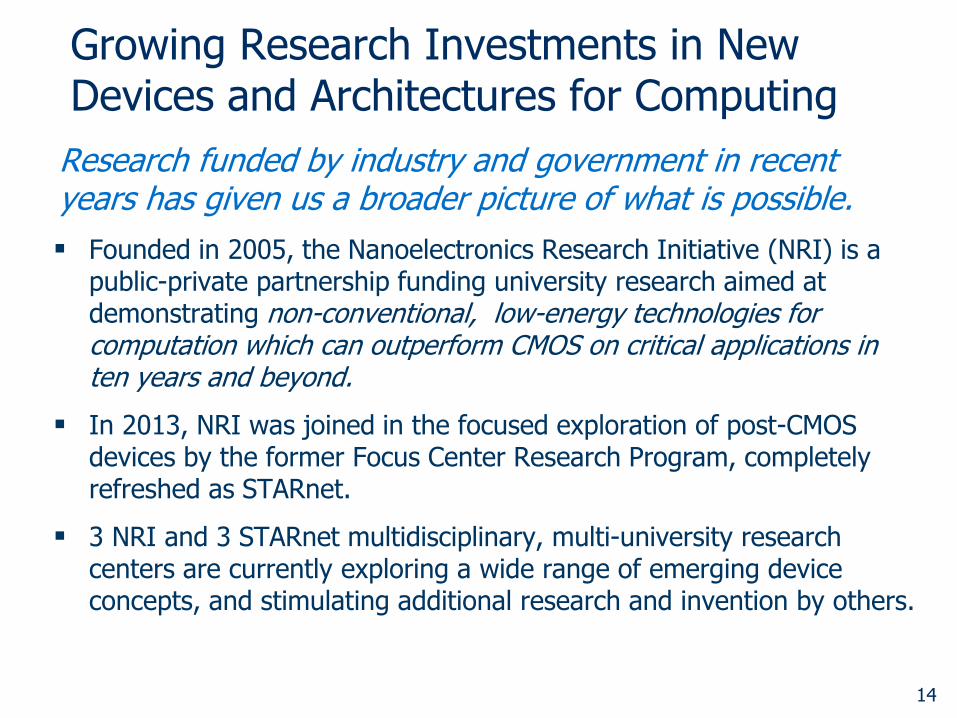
Growing Research Investments in New Devices and Architectures for Computing
Research funded by industry and government in recent years has given us a broader picture of what is possible.
Founded in 2005, the Nanoelectronics Research Initiative (NRI) is a public-private partnership funding university research aimed at demonstrating non-conventional, low-energy technologies for computation which can outperform CMOS on critical applications in ten years and beyond.
In 2013, NRI was joined in the focused exploration of post-CMOS devices by the former Focus Center Research Program, completely refreshed as STARnet.
3 NRI and 3 STARnet multidisciplinary, multi-university research centers are currently exploring a wide range of emerging device concepts, and stimulating additional research and invention by others.
14
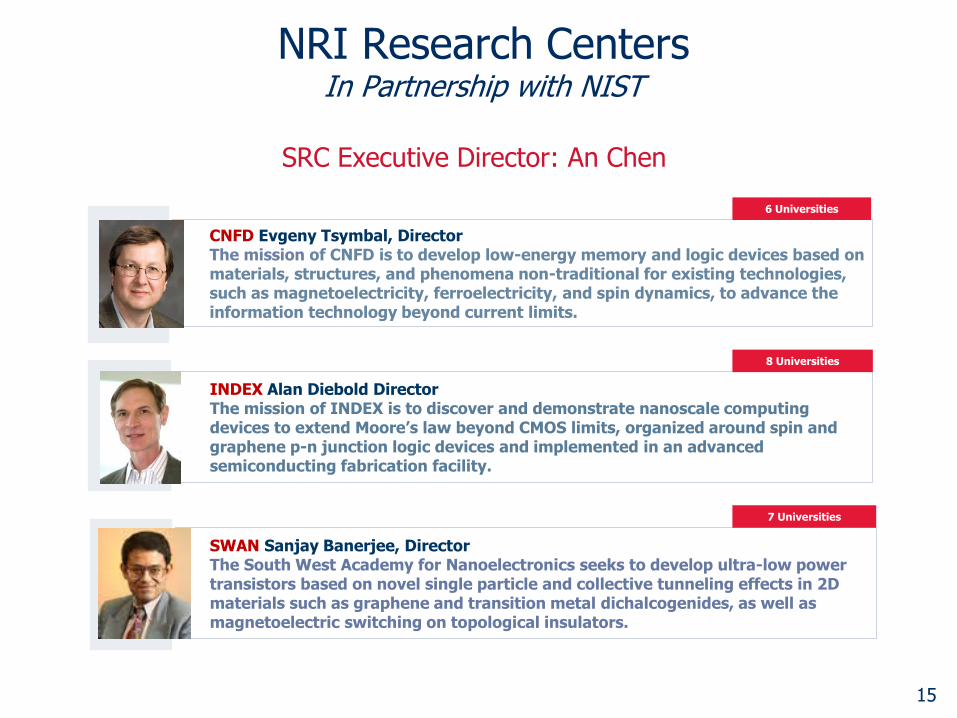
NRI Research CentersIn Partnership with NIST
15
INDEX Alan Diebold DirectorThe mission of INDEX is to discover and demonstrate nanoscale computing devices to extend Moore’s law beyond CMOS limits, organized around spin and graphene p-n junction logic devices and implemented in an advanced semiconducting fabrication facility.
8 Universities
SWAN Sanjay Banerjee, DirectorThe South West Academy for Nanoelectronics seeks to develop ultra-low power transistors based on novel single particle and collective tunneling effects in 2D materials such as graphene and transition metal dichalcogenides, as well as magnetoelectric switching on topological insulators.
7 Universities
SRC Executive Director: An Chen
CNFD Evgeny Tsymbal, Director The mission of CNFD is to develop low-energy memory and logic devices based on materials, structures, and phenomena non-traditional for existing technologies, such as magnetoelectricity, ferroelectricity, and spin dynamics, to advance the information technology beyond current limits.
6 Universities

STARnet Research CentersIn Partnership with DARPA
16
Applied Materials
Novellus
FAME Jane Pei-Chen Chang, Director The mission of FAME is to create and investigate new nonconventional atomic scale engineered materials and structures of multi-function oxides, metals and semiconductors to accelerate innovations in analog, logic and memory devices for revolutionary impact on the semiconductor and defense industries.
TerraSwarm Edward A. Lee, Director
The TerraSwarm Research Center aims to enable the simple, reliable, and secure deployment of a multiplicity of advanced distributed sense control-actuate applications on shared, massively distributed, heterogeneous, and mostly uncoordinated swarm platforms through an open and universal systems architecture.
C-SPIN Jian-Ping Wang, DirectorThe Center for Spintronic Materials, Interfaces and Novel Architectures (C-SPIN) seeks to overcome barriers to realizing practical spin-based memory and logic technology by assembling experts in magnetic materials, spin transport, novel spin-transport materials, spintronic devices, circuits, and novel architectures.
SONIC Naresh Shanbhag, DirectorSONIC will be guided by the following mission: To enable equivalent scaling in beyond-CMOS nanoscalefabrics by embracing their statistical attributes within statistical-inference-based applications, architectures, and circuits, to achieve unprecedented levels of robustness and energy efficiency.
LEAST Alan Seabaugh, Director
The Center for Low Energy Systems Technology (LEAST) explores the physics of new materials and devices to enable more energy-efficient integrated circuits and systems.
C-FAR Todd Austin, Director
The center's research agenda is guided by three initial technical vectors, whose intersections will help realize non-conventional architectures that address these pressing challenges: data-centric architectures, novel architectures based on emerging technologies, and beyond homogenous parallelism.
16 Universities 10 Universities
15 Universities
8 Universities14 Universities
10 Universities
SRC Executive Director: Gilroy Vandentop
Beyond-CMOS Devices
NewArchitectures
“Steep Slope” Devices
17
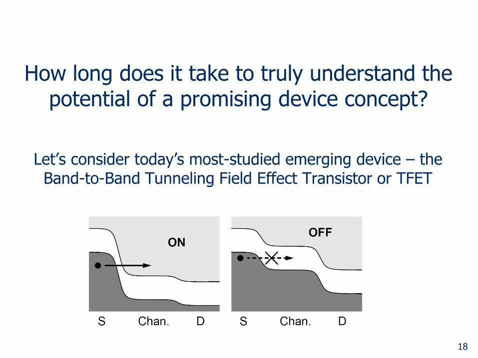
How long does it take to truly understand the potential of a promising device concept?
18
Let’s consider today’s most-studied emerging device – the Band-to-Band Tunneling Field Effect Transistor or TFET

A Very Brief History of TFET Research
1989: First report of gated tunnelingS. Banerjee et al., IEEE Electron Device Lett. EDL-8, pp. 347–349, Aug. 1987.
2005: SS less than 60 mV/decade in CNT TFETAppenzeller, et al., Phys. Rev. Lett. 93, art. 196805, Nov. 2004.
2007: DARPA STEEP program focuses on Si and Si-Ge TFETs
2009: III-V broken-gap heterojunction TFET proposedS. O. Koswatta et al., IEDM 2009.
2013: Prediction of new ultra-low power design space opened by TFETs U. Avci and I. Young, IEDM 2013.
Current:
New TFET variants continue to emerge (i.e. graded composition nitrides; P. Fay et al., Notre Dame)
But subthreshold slope in high-current (i.e. fast switching) devices continues to disappoint, and the fundamental leakage mechanisms that may explain this are still poorly understood.
19
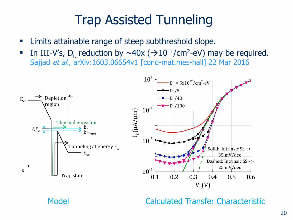
Trap Assisted Tunneling
Limits attainable range of steep subthreshold slope.
In III-V’s, Dit reduction by ~40x (1011/cm2-eV) may be required. Sajjad et al., arXiv:1603.06654v1 [cond-mat.mes-hall] 22 Mar 2016
20
Model Calculated Transfer Characteristic

1
1’
2
2’
Δ𝐸
1
1’
2
2’
Γ-band
heavy-holeband
initialstates
recombination
CHCCgeneration
𝐸
𝑘𝑥, 𝑘𝑦
1
1’
2
2’
1
1’
2
2’
initialstates
recombination
HCHHgeneration
inverse processes
initialstates
initialstates
dominant in p-TFETs dominant in n-TFETs
Generation/RecombinationA fundamental leakage mechanism
J. J. Teherani, et al., J. Appl. Phys. 120, 084507 (2016)

Newer steep slope device concepts continue to emerge.
Negative Capacitance FETSalahuddin and Datta, Nano Lett., 2008, 8 (2), pp 405–410.
Graphene p-n Junction (GPNJ) DeviceNRI INDEX center R.N. Sajjad and A. W. Gosh, arXiv:1305.7171, May 2013
Piezoelectronic Transistor (PET; solid-state relay)D.M. Newns, B.G. Elmegreen, X.-H. Liu and G.J. Martyna, J. Appl. Phys., vol. 111, art. 084509, 2012
PiezoFETSTARnet LEAST centerR. K. Jana, G. L. Snider, and D. Jena, physica status solidi (c), vol. 10, no. 11, pp. 1469-1472, November 2013
and more …
22

Electrostrictive Field Effect TransistorSaptarshi Das, Scientific Reports, 2016; 6: 34811.
voltage pressure transduction enables steep slope
Predicted high ON current
23

Nanomagnetic Devices
24
25IEDM Short Course; Beyond CMOS: Emerging Materials and Devices, R. Allenspach
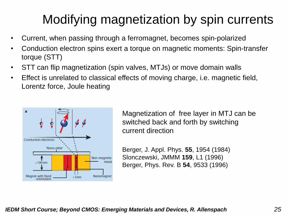
Berger, J. Appl. Phys. 55, 1954 (1984)
Slonczewski, JMMM 159, L1 (1996)
Berger, Phys. Rev. B 54, 9533 (1996)
Modifying magnetization by spin currents
• Current, when passing through a ferromagnet, becomes spin-polarized
• Conduction electron spins exert a torque on magnetic moments: Spin-transfer
torque (STT)
• STT can flip magnetization (spin valves, MTJs) or move domain walls
• Effect is unrelated to classical effects of moving charge, i.e. magnetic field,
Lorentz force, Joule heating
Magnetization of free layer in MTJ can be
switched back and forth by switching
current direction
26IEDM Short Course; Beyond CMOS: Emerging Materials and Devices, R. Allenspach
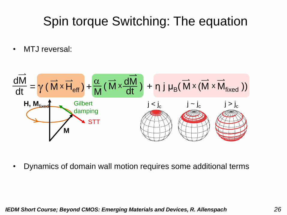
Spin torque Switching: The equation
• MTJ reversal:
M
H, MfixedGilbert
damping
STT
( M x )dM
= ( M x Heff ) +g dtdMdt
a
M+ η j μB( M x (M x Mfixed ))
• Dynamics of domain wall motion requires some additional terms
j < jc j ~ jc j > jc
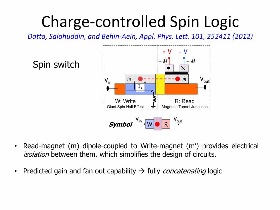
• Read-magnet (m) dipole-coupled to Write-magnet (m’) provides electricalisolation between them, which simplifies the design of circuits.
• Predicted gain and fan out capability fully concatenating logic
Spin switch
Symbol
Charge-controlled Spin LogicDatta, Salahuddin, and Behin-Aein, Appl. Phys. Lett. 101, 252411 (2012)
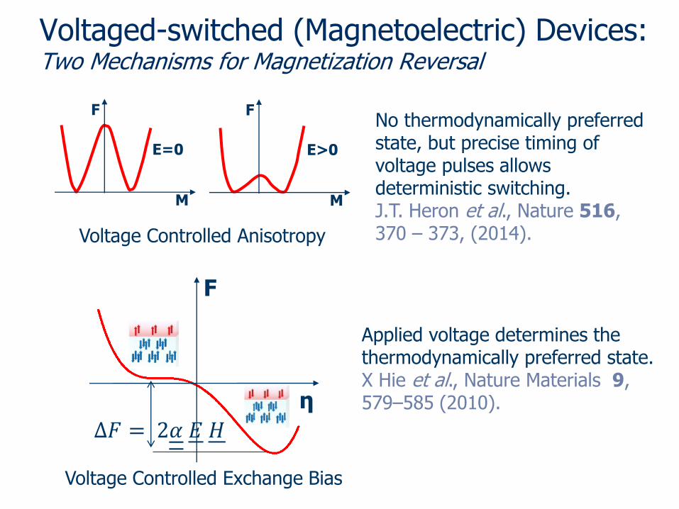
Voltaged-switched (Magnetoelectric) Devices:Two Mechanisms for Magnetization Reversal
F
M
E=0
F
M
E>0
F
η
Δ𝐹 = 2𝛼 𝐸 𝐻
Voltage Controlled Exchange Bias
Voltage Controlled Anisotropy
No thermodynamically preferred state, but precise timing of voltage pulses allows deterministic switching.J.T. Heron et al., Nature 516, 370 – 373, (2014).
Applied voltage determines the thermodynamically preferred state. X Hie et al., Nature Materials 9, 579–585 (2010).
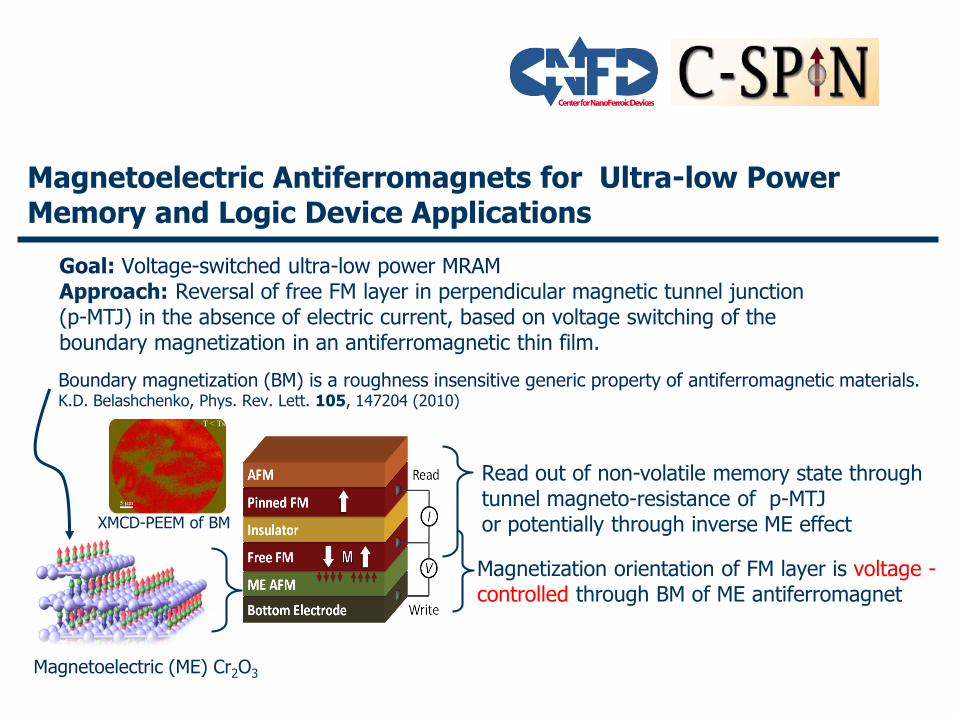
Magnetoelectric Antiferromagnets for Ultra-low Power Memory and Logic Device Applications
Goal: Voltage-switched ultra-low power MRAMApproach: Reversal of free FM layer in perpendicular magnetic tunnel junction (p-MTJ) in the absence of electric current, based on voltage switching of the boundary magnetization in an antiferromagnetic thin film.
Magnetoelectric (ME) Cr2O3
Magnetization orientation of FM layer is voltage -controlled through BM of ME antiferromagnet
Boundary magnetization (BM) is a roughness insensitive generic property of antiferromagnetic materials.K.D. Belashchenko, Phys. Rev. Lett. 105, 147204 (2010)
XMCD-PEEM of BM
Read out of non-volatile memory state through tunnel magneto-resistance of p-MTJor potentially through inverse ME effect
30
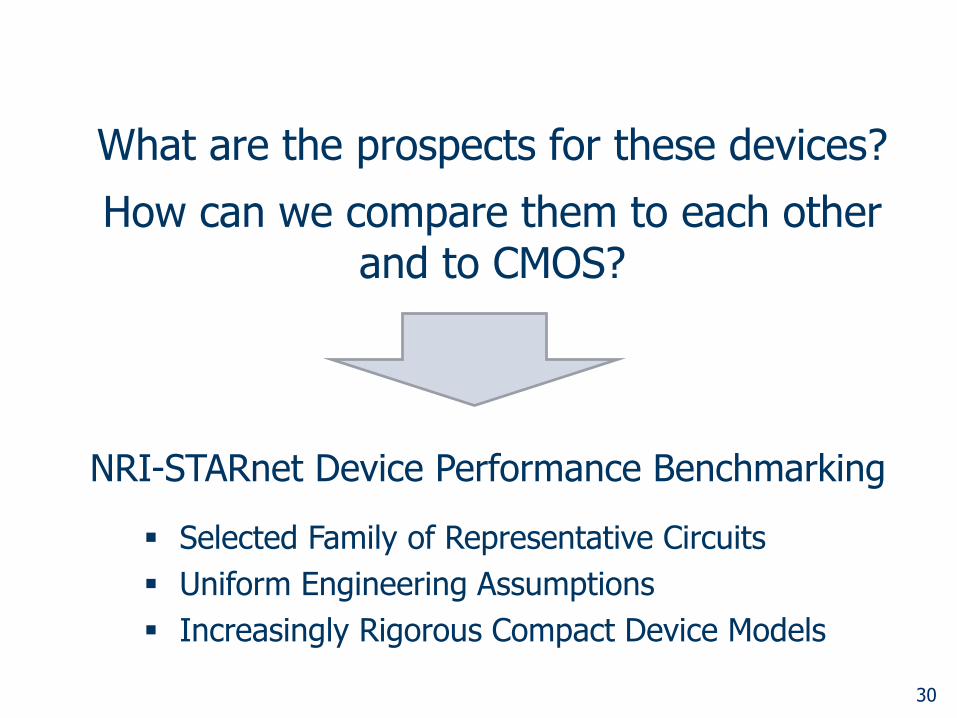
What are the prospects for these devices?
How can we compare them to each other and to CMOS?
NRI-STARnet Device Performance Benchmarking
Selected Family of Representative Circuits
Uniform Engineering Assumptions
Increasingly Rigorous Compact Device Models
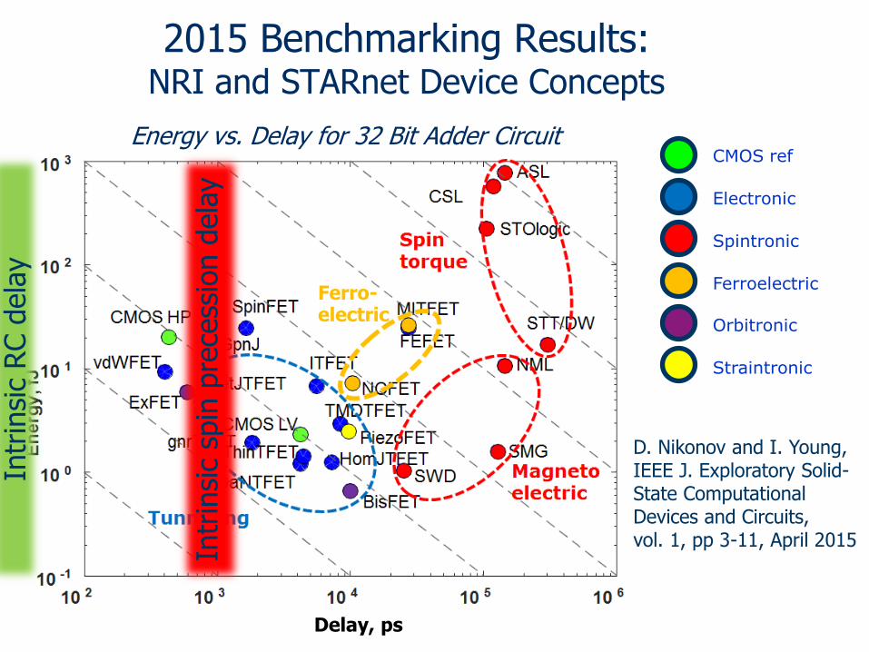
Delay, ps
D. Nikonov and I. Young, IEEE J. Exploratory Solid-State Computational Devices and Circuits,vol. 1, pp 3-11, April 2015
2015 Benchmarking Results:NRI and STARnet Device Concepts
CMOS ref
Electronic
Spintronic
Ferroelectric
Orbitronic
Straintronic
Energy vs. Delay for 32 Bit Adder Circuit
Ferro-electric
Intr
insi
c RC d
ela
y
Intr
insi
c sp
in p
rece
ssio
n d
ela
y
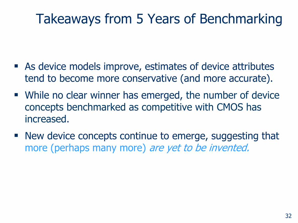
Takeaways from 5 Years of Benchmarking
As device models improve, estimates of device attributes tend to become more conservative (and more accurate).
While no clear winner has emerged, the number of device concepts benchmarked as competitive with CMOS has increased.
New device concepts continue to emerge, suggesting that more (perhaps many more) are yet to be invented.
32
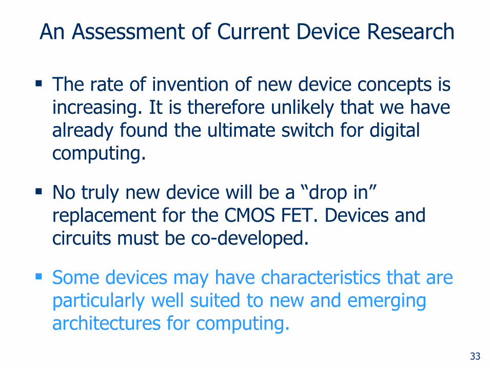
An Assessment of Current Device Research
The rate of invention of new device concepts is increasing. It is therefore unlikely that we have already found the ultimate switch for digital computing.
No truly new device will be a “drop in” replacement for the CMOS FET. Devices and circuits must be co-developed.
Some devices may have characteristics that are particularly well suited to new and emerging architectures for computing.
33

34
As one example of a broad class increasingly important architectures,
consider a Feed–forward Neural Network.
The computation in each node is simple.
Can it be done by a single device?

35
Spin-Neuron Based Feed-Forward Neural NetworkSharad, Fan, Roy et al. DAC 2013/ TNANO 2014/ JAP 1014
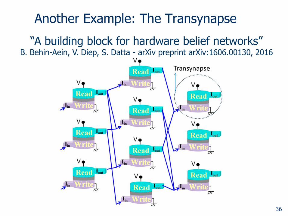
Another Example: The Transynapse
36
“A building block for hardware belief networks”B. Behin-Aein, V. Diep, S. Datta - arXiv preprint arXiv:1606.00130, 2016
The Unexplored Research Landscape:
New Devices and New Architectures
37

E2CDA Energy Efficient Computing: from Devices to ArchitecturesFunding 15 Universities in 10 States
Electronic-Photonic Integration Using the Transistor Laser for Energy-Efficient ComputingU. Illinois/Urbana-Champaign, U. Chicago
EXtremely Energy Efficient Collective ELectronics (EXCEL)Notre DamePenn State, U. ChicagoGeorgia Tech, UC-San Diego
2D Electrostrictive FETs for Ultra-Low Power Circuits and ArchitecturesPenn State
Memory, Logic, and Logic in Memory Using Three Terminal Magnetic Tunnel JunctionsMIT
Center forExcitonic DevicesUC-San DiegoMIT UC-Santa BarbaraPrinceton
Energy Efficient Learning Machines (ENIGMA)UC-Berkeley Stanford A Fast 70mV Transistor
Technology for Ultra-Low-Energy ComputingUC-Santa BarbaraU. VirginiaPurdue
Energy Efficient Computing with Chip-Based PhotonicsColumbiaMITStanfordUC-San Diego
Self-Adaptive Reservoir Computing with Spiking Neurons: Learning Algorithms and Processor ArchitecturesTexas A&M
Conclusion
Looking beyond conventional FETsand the von-Neumann architecture,
there is a lot to explore!
Exploration of new devices and architectures for computing will drive
materials research for many more years.
39

Thanks!
40