Embed Size (px)
Citation preview
Electronic and optical properties of the LiCdX (X=N, P, As and Sb)filled-tetrahedral compounds with the Tran–Blaha modifiedBecke–Johnson density functional
A. Bouhemadou a,*, S. Bin-Omran b,c, D. Allali a, S.M. Al-Otaibi b, R. Khenata d,Y. Al-Douri e, M. Chegaar f, A.H. Reshak g,h
a Laboratory for Developing New Materials and their Characterization, University of Setif 1, Setif 19000, AlgeriabDepartment of Physics and Astronomy, College of Science, King Saud University, P.O. Box 2455, Riyadh 11451, Saudi ArabiacDepartment of Physics, Faculty of Science & Humanitarian Studies, Salman Bin Abdalaziz University, Alkharj 11942, Saudi Arabiad Laboratoire de Physique Quantique et de Modélisation Mathématique (LPQ3M), Département de Technologie, Université de Mascara, Mascara 29000, Algeriae Institute of Nano Electronic Engineering, Universiti Malaysia Perlis, Kangar, Perlis 01000, MalaysiafDepartment of Physics, Faculty of Science, University of Setif 1, Setif 19000, AlgeriagNew Technologies-Research Center, University of West Bohemia, Univerzitni 8, Pilson 306 14, Czech RepublichCenter of Excellence Geopolymer and Green Technology, School of Material Engineering, University Malaysia Perlis, Kangar, Perlis 01007, Malaysia
A R T I C L E I N F O
Article history:Received 5 April 2014Received in revised form 26 August 2014Accepted 3 January 2015Available online 5 January 2015
Keywords:A. SemiconductorsD. Electronic structureD. Optical properties
A B S T R A C T
The structural, electronic and optical properties of the LiCdN, LiCdP, LiCdAs and LiCdSb filled-tetrahedralcompounds have been explored fromfirst-principles. The calculated structural parameters are consistentwith the available experimental results. Since DFT with the common LDA and GGA underestimates theband gap, we use a new developed functional able to accurately describe the electronic structure ofsemiconductors, namely the Tran–Blaha-modified Becke–Johnson potential. The four investigatedcompounds demonstrate semiconducting behavior with direct band gap ranging from about 0.32 to1.65 eV. The charge-carrier effective masses are evaluated at the topmost valence band and at thebottommost conduction band. The evolution of the value and nature of the energy band gap underpressure effect is also investigated. The frequency-dependent complex dielectric function and somemacroscopic optical constants are estimated. The microscopic origins of the structures in the opticalspectra are determined in terms of the calculated energy band structures.
ã 2015 Elsevier Ltd. All rights reserved.
1. Introduction
The development and optimization of optoelectronic devicescrucially depend on the availability of suitable semiconductormaterials. The ternary and higher multinary semiconductorcompounds provide a wide range of electronic and opticalproperties to choose for the respective technological applications.A particular interesting class of ternary materials are the eightvalence electrons I–II–V type, such as the Nowotny–Juza AIBIICV
compounds [1,2] (where the Roman numerals indicate theappropriate column of the periodic table, i.e., AI = Li, Na, Cu, Ag;BII =Mg, Zn, Cd and CV =N, P, As, Sb and Bi). The Nowotny–JuzaAIBIICV compounds are also called “filled zinc-blende structure” or“filled-tetrahedral compounds” (FTC). The filled-tetrahedral
compounds AIBIICV (e.g., LiCdP) constitute an interesting class ofgenerally direct gap semiconductors closely related to the morefamiliar III–V compounds (e.g., InP is the binary analogous toLiCdP) [3–7]. A number of these materials were synthesized andstructurally characterized by Nowotny [1] and Juza [2] a long timeago. Interest in this family compounds has been renewed since theprediction of Wood et al. [3], and Carlson et al. [4] that thefilled-tetrahedral compounds LiZnP and LiZnN exhibit semicon-ducting character with a direct energy band gap, and hence theyare very prominent materials for photovoltaic and some othertechnological applications. This prediction has stimulatednumerous experimental and theoretical works; consequentlyseveral compounds of this class have been synthesized andcharacterized [5–38].
Most of the filled-tetrahedral compounds AIBIICV (e.g., LiCdP)usually crystallize in a cubic structure which can be obtained fromthe zinc-blende DIIICV (e.g., InP) by transmuting the DIII (e.g., Inatom) to the isovalent AI + BII (Li + Cd) atom pair. The familiar
* Corresponding author. Tel.: +213 553163456; fax: +213 36620136.E-mail address: [email protected] (A. Bouhemadou).
http://dx.doi.org/10.1016/j.materresbull.2015.01.0030025-5408/ã 2015 Elsevier Ltd. All rights reserved.
Materials Research Bulletin 64 (2015) 337–346
Contents lists available at ScienceDirect
Materials Research Bulletin
journal homepage: www.elsevier .com/ locate /matresbu
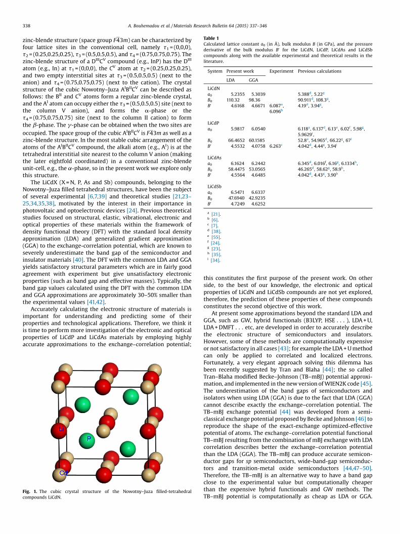
zinc-blende structure (space group F43m) can be characterized byfour lattice sites in the conventional cell, namely t1 = (0,0,0),t2 = (0.25,0.25,0.25), t3 = (0.5,0.5,0.5), and t4 = (0.75,0.75,0.75). Thezinc-blende structure of a DIIICV compound (e.g., InP) has the DIII
atom (e.g., In) at t1 = (0,0,0), the CV atom at t2 = (0.25,0.25,0.25),and two empty interstitial sites at t3 = (0.5,0.5,0.5) (next to theanion) and t4 = (0.75,0.75,0.75) (next to the cation). The crystalstructure of the cubic Nowotny–Juza AIBIICV can be described asfollows: the BII and CV atoms form a regular zinc-blende crystal,and the AI atom can occupy either the t3 = (0.5,0.5,0.5) site (next tothe column V anion), and forms the a-phase or thet4 = (0.75,0.75,0.75) site (next to the column II cation) to formthe b-phase. The g-phase can be obtained when the two sites areoccupied. The space group of the cubic AIBIICV is F43m as well as azinc-blende structure. In the most stable cubic arrangement of theatoms of the AIBIICV compound, the alkali atom (e.g., AI) is at thetetrahedral interstitial site nearest to the column V anion (makingthe later eightfold coordinated) in a conventional zinc-blendeunit-cell, e.g., the a-phase, so in the present work we explore onlythis structure.
The LiCdX (X=N, P, As and Sb) compounds, belonging to theNowotny–Juza filled tetrahedral structures, have been the subjectof several experimental [6,7,39] and theoretical studies [21,23–25,34,35,38], motivated by the interest in their importance inphotovoltaic and optoelectronic devices [24]. Previous theoreticalstudies focused on structural, elastic, vibrational, electronic andoptical properties of these materials within the framework ofdensity functional theory (DFT) with the standard local densityapproximation (LDA) and generalized gradient approximation(GGA) to the exchange-correlation potential, which are known toseverely underestimate the band gap of the semiconductor andinsulator materials [40]. The DFT with the common LDA and GGAyields satisfactory structural parameters which are in fairly goodagreement with experiment but give unsatisfactory electronicproperties (such as band gap and effective masses). Typically, theband gap values calculated using the DFT with the common LDAand GGA approximations are approximately 30–50% smaller thanthe experimental values [41,42].
Accurately calculating the electronic structure of materials isimportant for understanding and predicting some of theirproperties and technological applications. Therefore, we think itis time to perform more investigation of the electronic and opticalproperties of LiCdP and LiCdAs materials by employing highlyaccurate approximations to the exchange–correlation potential;
this constitutes the first purpose of the present work. On otherside, to the best of our knowledge, the electronic and opticalproperties of LiCdN and LiCdSb compounds are not yet explored,therefore, the prediction of these properties of these compoundsconstitutes the second objective of this work.
At present some approximations beyond the standard LDA andGGA, such as GW, hybrid functionals (B3LYP, HSE . . . ), LDA+U,LDA+DMFT . . . etc, are developed in order to accurately describethe electronic structure of semiconductors and insulators.However, some of these methods are computationally expensiveor not satisfactory in all cases [43]; for example the LDA+Umethodcan only be applied to correlated and localized electrons.Fortunately, a very elegant approach solving this dilemma hasbeen recently suggested by Tran and Blaha [44]; the so calledTran–Blaha modified Becke–Johnson (TB–mBJ) potential approxi-mation, and implemented in the newversion ofWIEN2K code [45].The underestimation of the band gaps of semiconductors andisolators when using LDA (GGA) is due to the fact that LDA (GGA)cannot describe exactly the exchange–correlation potential. TheTB–mBJ exchange potential [44] was developed from a semi-classical exchange potential proposed byBecke and Johnson [46] toreproduce the shape of the exact-exchange optimized-effectivepotential of atoms. The exchange–correlation potential functionalTB–mBJ resulting from the combination of mBJ exchangewith LDAcorrelation describes better the exchange–correlation potentialthan the LDA (GGA). The TB–mBJ can produce accurate semicon-ductor gaps for sp semiconductors, wide-band-gap semiconduc-tors and transition-metal oxide semiconductors [44,47–50].Therefore, the TB–mBJ is an alternative way to have a band gapclose to the experimental value but computationally cheaperthan the expensive hybrid functionals and GW methods. TheTB–mBJ potential is computationally as cheap as LDA or GGA.
[(Fig._1)TD$FIG]
Fig. 1. The cubic crystal structure of the Nowotny–Juza filled-tetrahedralcompounds LiCdN.
Table 1Calculated lattice constant a0 (in Å), bulk modulus B (in GPa), and the pressurederivative of the bulk modulus B0 for the LiCdN, LiCdP, LiCdAs and LiCdSbcompounds along with the available experimental and theoretical results in theliterature.
System Present work Experiment Previous calculations
LDA GGA
LiCdNa0 5.2355 5.3039 5.388d, 5.22g
B0 110.32 98.36 90.911d, 108.3g,B0 4.6168 4.6671 6.087a,
6.096b4.19d, 3.94g,
LiCdPa0 5.9817 6.0540 6.118a, 6.137d, 6.13e, 6.02f, 5.98g,
5.9629i,B0 66.4652 60.1585 52.8a, 54.965d, 66.22g, 67i
B0 4.5532 4.0758 6.263c 4.042d, 4.44g, 3.94i
LiCdAsa0 6.1624 6.2442 6.345d, 6.016f, 6.16g, 6.1334h,B0 58.4475 53.0565 46.265d, 58.62g, 58.9h,B0 4.5564 4.6485 4.042d, 4.43g, 3.90h
LiCdSba0 6.5471 6.6337B0 47.6940 42.9235B0 4.7249 4.6252
a [21].b [6].c [7].d [38].e [55].f [24].g [23].h [35].i [34].
338 A. Bouhemadou et al. /Materials Research Bulletin 64 (2015) 337–346
Therewith, one can obtain accurate band gaps. Detailed descriptionof the TB–mBJ and its merits and limits can be found in Refs.[44–50]. Tran and Blaha [44] have demonstrated that the TB–mBJpotential yields band gaps which are in good agreement withexperiment, leading to typical errors of less than 10% for somesemiconductors and insulators. In the present work, we aim tocalculate the electronic and optical properties of the LiCdN, LiCdP,LiCdAs, and LiCdSb materials, using the LDA [51], GGA–PBEsol [52]and Engel–Vosko scheme of the GGA (GGA–EV) [53] functionalsand to compare that to the obtained results using the TB–mBJfunctional [44–46] in order to show the advantage of the TB–mBJfor describing electronic structure of the considered materials.
The remainder of the paper is organized as follows: In Section 2,a brief outline of the method of calculation is given. The obtainedresults and some discussions are presented in Section 3. Someconcluding remarks are given in Section 4.
2. Computational details
Ab initio calculations were performed in the framework ofdensity functional theory (DFT) with an all-electron method usingthe linearized/augmented plane wave+ local orbitals (L/APW+ lo)basis set as implemented in theWIEN2k code [45]. In this method,the wave functions are expanded in a linear combination of radialfunctions time spherical harmonics inside the non-overlappingmuffin-tin spheres of radius RMT surrounding each atom and inplane waves in the interstitial region between the spheres. Theradii of the muffin-tin spheres were taken as large as possiblewithout overlapping the spheres. The maximum l of the expansionof the wave function in spherical harmonics inside the muffin-tin
spheres was lmax = 10. A plane-wave cut-off of Kmax = 4.0 (a.u.)�1 ischosen for the expansion of the wave functions in the interstitialregion. The k integrations over the Brillouin zone (BZ) areperformed up to 10�10�10 Monkorst–Pack mesh (MP) [54](47 k-points in the irreducible Brillouin zone (IBZ)). Theself-consistent calculations are considered converged when thetotal energy of the system is stable within 10�5 Ry. Theexchange–correlation potential for the structural properties wascalculated using the LDA [51] and the GGA based on Perdew et al.(GGA–PBEsol) [52]. For the electronic properties, in addition to theLDA and the GGA, the GGA–EV [53] and the TB–mBJ [44–46],which better describe many semiconductors and insulators,were applied.
The linear optical properties of a material can be described bythe complex dielectric function e(v) = e1(v) + ie2(v). The imaginarypart of the dielectric function e2(v) represents the absorption inthe crystal, which can be calculated from the momentum matrixelements between the occupied and the unoccupied wavefunctions [55]:
ImeabðvÞ ¼ eab2 ðvÞ¼ 4pe2
m2v2
Xi;f
Zf jpajih i ijpbjf
D EWið1�Wf ÞðEf � Ei
� �hvÞd3k:
In this expression, f jpajih i and f jpbjiD E
are the dipole matrix
elements corresponding to thea and ß directions of the crystal (x,yor z), and f(i) is the final (initial) state. Wn is the Fermi distributionfunction for the nth state, and En is the electron energy in the nthstate. The real part of the frequency-dependent dielectric function
[(Fig._2)TD$FIG]
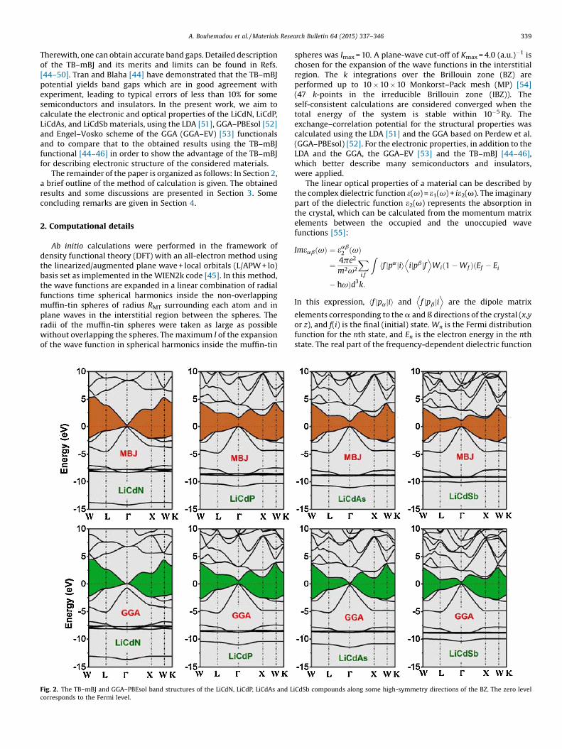
Fig. 2. The TB–mBJ and GGA–PBEsol band structures of the LiCdN, LiCdP, LiCdAs and LiCdSb compounds along some high-symmetry directions of the BZ. The zero levelcorresponds to the Fermi level.
A. Bouhemadou et al. /Materials Research Bulletin 64 (2015) 337–346 339
expression eab1 ðvÞ is computed from eab2 ðvÞ using theKramers–Kronig relations in the form:
eab1 ðvÞ ¼ dab þ 2pPZ1
0
v0eab2 ðv0Þv02 �v2 dv
0; ,
where P is the Cauchy principal value of the integral. With theknowledge of the complex dielectric tensor components all otherfrequency-dependent optical constants, such as the refractiveindex n(v), the extinction coefficient k(v), the reflectivity R(v), thecoefficient of absorption a(v) and the loss function L(v), can becalculated using the well-known relations. For the cubic structure,the optical properties are isotropic, i.e., there is only oneindependent component (exx). The optical spectra strongly dependon the BZ sampling, therefore the momentummatrix elements areexplicitly evaluated at a large number of k-points in the BZ(30�30�30 k-points mesh).
3. Results and discussions
3.1. Structural properties
The crystal structure of LiCdN is shown in Fig. 1. The groundstate properties, namely equilibrium lattice constant a, bulkmodulus B and pressure derivative of the bulk modulus B0 aredetermined by fitting the calculated total energy versus unit cellvolume data to the Birch–Murnaghan equation of state [56,57]. InTable 1, we give the obtained results for the computed ground stateparameters using both the LDA and GGA to the exchange–correlation potential, and make a comparison with availableexperimental [6,7,21] and theoretical data [21,23,34,35,38,58]. Asseen in Table 1, agreement between the lattice constants(experiment and optimized) is excellent in the case of theGGA–PBEsol calculations (with the largest deviation betweenthe experimental and calculated lattice constants being 0.5% forthe LiCdP). In the case of the LDA results, the maximum deviationwas found to be 1.7%. It can be noted that as a result of substitutionsof N by P, P byAs and As by Sb, the lattice constant a increases in thefollowing sequence: a(LiCdN)< a(LiCdP)< a(LiCdAs)< a(LiCdSb)(1). This trend can be easily explained by considering the atomicradii (R) of the N, P, As and Sb atoms, which increase in the samesequence: R(N) = 0.75Å<R(P) = 1.23Å<R(As) =<R(P) = 1.33Å<R(Sb) = 1.53Å. This consistency proves the reliability and theaccuracy of these present ab initio calculation findings and givesconfidence in the results of the following calculations of theelectronic and optical properties for the considered materials. Wedid notfind any experimental results for the bulkmodulus B and itspressure derivative B0 in the literature to support these theoreticalresults. Our obtained values for B and B0 are reasonably consistent
Table 2Calculated direct band gap Γ–Γ and indirect band gap Γ–X values of LiCdN, LiCdP,LiCdAs and LiCdSb with LDA, GGA–PBEsol, GGA–EV and TB–mBJ functionalscompared with the available literature.
LiCdN LiCdP LiCdAs LiCdSb
G–G G–X G–G G–X G–G G–X G–G G–X
PresentLDA 0.00 1.98 0.64 1.2 0 1.02 0.31 0.89GGA 0.00 1.94 0.61 1.26 0 1.07 0.27 0.94GGA-EV
0.00 2.69 1.455 2.27 0.715 2 0.94 1.56
TB-mBJ
0.32 3.1 1.65 2.06 0.96 1.82 1.1 1.55
Expt. 1.30a,Others 0.00g 0.635b, .91d, 0.85e,
0.556f1.189b
1.33d0.05c
0.00f0.93c
1.25g
a [6].b [25].c [35].d [34].e [21].f [38].g [55].
Table 3Calculated effective masses of the electron ðm�
eÞ, the heavy hole ðm�hhÞ and the
light hole ðm�lhÞ (in units of free electron mass m0) for the LiCdN, LiCdP,
LiCdAs and LiCdSb compounds.
LiCdN LiCdP LiCdAs LiCdSbG–L G–X G–L G–X G–L G–X G–L G–X
m�e 0.081 0.089 0.17 0.18 0.096 0.107 0.101 0.111
m�hh
2.08 0.977 1.066 0.453 0.985 0.415 0.778 0.319m�
lh0.078 0.118 0.144 0.176 0.092 0.107 0.084 0.103
[(Fig._3)TD$FIG]
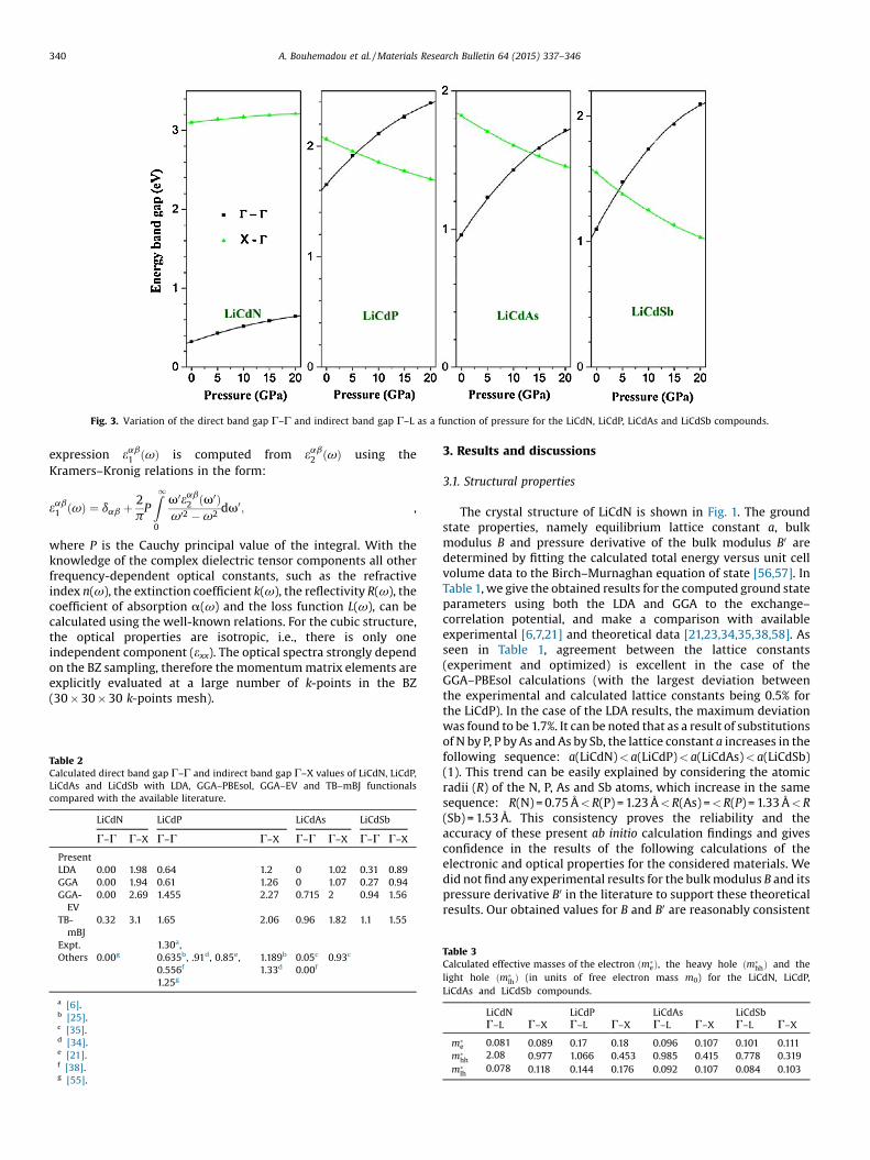
Fig. 3. Variation of the direct band gap Γ–Γ and indirect band gap Γ–L as a function of pressure for the LiCdN, LiCdP, LiCdAs and LiCdSb compounds.
340 A. Bouhemadou et al. /Materials Research Bulletin 64 (2015) 337–346
with those previously obtained using ab initio calculations[21,23,34,35,38]. The bulk modules of the considered materialsincrease in the sequence: B(LiCdN) >B(LiCdP) >B(LiCdAs) >B(LiCdSb), i.e., in reverse sequence to (1); this is in agreement withthe known relation between the cell volume V and the bulkmodulus B: B�V�1.
3.2. Electronic properties
The electronic band structures of the four considered materialsare calculated with their optimized crystal structure parametersusing four different functional: the LDA, the GGA–PBEsol, theGGA–EVand theTB–mBJ.Wenote that, because there isnoexchangeandcorrelationenergy term fromwhichtheTB–mBJpotential canbededuced, a direct optimization procedure is not possible as in theusual theory [59]. The GGA–EV functional is obtained by optimizingthe exchange-correlation potential Vex rather than the energyEex, and it is designed to improve thebandgaps rather than the localenergy. Consequently, the equilibrium lattice constant calculatedusing this functional is considerably larger than the experimentalvalue [60]. Therefore, the band structures using the TB–mBJ andGGA–EV functionals were calculated with the lattice parametervalues that were obtained using the GGA–PBEsol functional. Theoverall band profiles are qualitatively similar to those previouslyreported [21,25,34,35,38,58], but there are quantitative differencesresulting from the use of the GGA–EV and the TB–mBJ functional,and these are important. The upper valence band maximum(UVBM) and the lower conduction bandminimum (LCBM) occur atΓ point; thus the four investigatedmaterials are direct energy bandgap semiconductors. In Fig. 2, we compare the band structure forLiCdN, LiCdP, LiCdAs and LiCdSb calculated with the GGA–PBEsoland with the TB–mBJ potential. As a general result, the TB–mBJcauses a rigiddisplacementof the conductionbands towardshigherenergies with respect to the top of the valence band, with small
differences in the dispersion at some regions of the Brillouinzone. The pattern of the band structures in LiCdP, LiCdAs andLiCdSb is almost similar but somewhat different from that ofLiCdN, which will explain the noted differences between theoptical spectra of LiCdN and the other considered compounds.After analyzing the results (Table 2), we have classified them inthree groups; the first group contains the common LDA andGGA–PBEsol functionals. Both LDA and GGA–PBEsol yield a zeroband gap for the LiCdN and LiCdAs compounds. The band gap valueof LiCdP which is calculated within this first group is significantlyless than the experimental value; there is experimental band gapvalue only for the LiCdP compound. The second group containsGGA–EV and predicts a band gap value for LiCdP which iscomparable with the experimental result, but GGA–EV predicts azero band gap for LiCdN. The third group contains TB–mBJ asExc functional and predicts the four considered materials assemiconductors with appreciable band gap values. There is onlyone experimental value for the band gap of the LiCdP compoundand we have no idea about the accuracy of this measurement,therefore one needs more experimental data to make a reasonablecomparison between the obtained results using TB–mBJ and themeasured ones. Obviously the TB–mBJ functional significantlyimproves the band gap value compared to the common LDA andGGA, thus we will discuss the rest of the electronic and opticalproperties obtained within the TB–mBJ.
The pressure effects on the electronic and optical propertiesweremodeled by calculating the optimized lattice parameter (a) ata set of fixed pressures (P =0, 5, 10, 15 and 20GPa) then calculatingthese properties at these optimized geometries. The procedures tocalculate the optimized lattice parameter a at a fixed pressure P areas follows: after obtaining the bulk modulus B and its pressurederivative B0 according to the procedure explained in Section 3.1,the Murnaghan equation of state [56]: V=V0(1 +B0(P/B))�1/B0
,where V0 denotes the unit cell volume at zero pressure, is used to
[(Fig._4)TD$FIG]
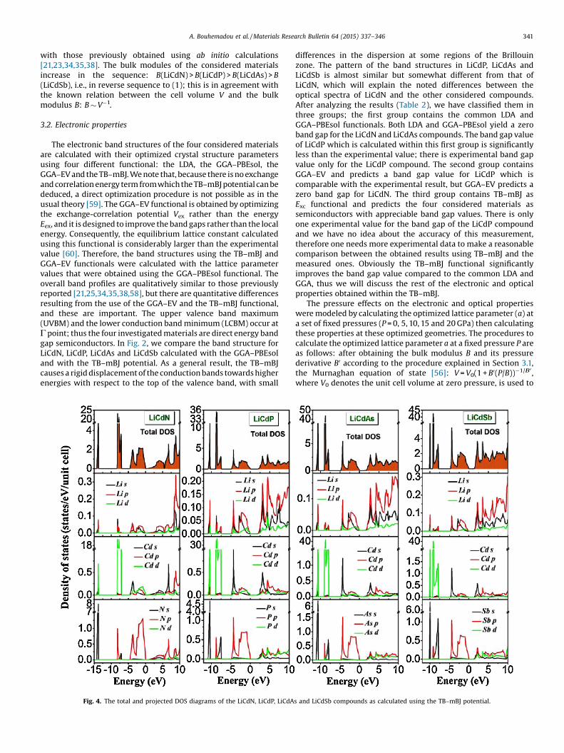
Fig. 4. The total and projected DOS diagrams of the LiCdN, LiCdP, LiCdAs and LiCdSb compounds as calculated using the TB–mBJ potential.
A. Bouhemadou et al. /Materials Research Bulletin 64 (2015) 337–346 341
calculate the value of the unit cell volume V corresponding tothe fixed pressured P then calculating the correspondinglattice parameter a. Fig. 3 shows that in the LiCdN compound,both the fundamental direct band gap Γ–Γ and the indirectband gap Γ–X increase in a non-linear manner when thepressure is enhanced. However, in the LiCdP, LiCdAs and LiCdSbcompounds, when the pressure is enhanced, the fundamentaldirect band gap Γ–Γ increases but the indirect band gap decreasesin a non-linear manner. Therefore, a crossover between the directband gapΓ–Γ and the indirect band gapΓ–X curves occurs at 5.69,13.14 and 4.24GPa in LiCdP, LiCdAs and LiCdSb, respectively. Thevariation of the direct (Γ–Γ) and indirect (Γ–X) band gaps forLiCdN, LiCdP, LiCdAs and LiCdSb are fitted to the followingquadratic functions:
EðG�GÞg ðLiCdNÞ ¼ 0:32þ 2:25� 10�2p� 3:23� 10�4p2
EðG�XÞg ðLiCdNÞ ¼ 3:10þ 0:80� 10�2p� 1:43� 10�4p2
EðG�GÞg ðLiCdPÞ ¼ 1:65þ 5:45� 10�2p� 9:085� 10�4p2
EðG�XÞg ðLiCdPÞ ¼ 2:06� 2:28� 10�2pþ 2:40� 10�4p2
EðG�GÞg ðLiCdAsÞ ¼ 0:956þ 5:63� 10�2p� 9:51� p2
EðG�XÞg ðLiCdAsÞ ¼ 1:82� 2:41� 10�2pþ 2:97� 10�4p2
EðG�GÞg ðLiCdSbÞ ¼ 1:098þ 7:71� 10�2p� 14:10� p2
EðG�XÞg ðLiCdSbÞ ¼ 1:548� 2:44� 10�2pþ 4:468� 10�4p2
The energy is in eV and the pressure p is in GPa.The effective charge-carrier mass is one of themain factors that
determine the transport properties and electrical conductivity of amaterial. In general, smaller effective masses of the carrierscorrespond to the faster photogenerated carriers. Consequently, alow effective mass can promote carrier migration and suppresscarrier recombination. Here, the effective charge-carrier mass m*was evaluated by fitting the E–k diagram near the valence-bandmaximum (VBMa) and the conduction-band minimum (CBMi)with a parabolic variation. The effective mass m* (in unit of m0,wherem0 denotes the electron restmass) at a given point along the
direction given by ~k!
is:
1m� ¼ m0
�h2
@2EðkÞ@2k
The evaluated effective charge-carrier masses, at the G pointfrom the band dispersions of the VBMa and CBMi towards the Xand L directions in the Brillouin zone, are summarized in Table 3 forthe four considered materials. The effective electron mass,the heavy-hole mass and the light-hole mass are indicated bythe subscripts “e”ðm�
eÞ, “hh” ðm�hhÞ, and “hl” ðm�
hlÞ, respectively. Thecalculated CB electron effectivemass of LiCdN is slightly lower thanthose of LiCdP, LiCdAs and LiCdSb. Consequently, the mobility ofthe CB electrons and the electrical conductivity in LiCdN should beslightly higher. From Fig. 2, we note that (i) the electronic states atthe conduction-band minimum are more dispersive than thetopmost valence-band states; consequently, the conduction-bandelectrons have lower effectivemasses than the valence-band heavyholes, and the influence of the latter on the electrical conductivityis minimal; (ii) the effective masses of electrons in the consideredmaterials for the G!X and G! L directions in the BZ arepractically equal; hence, the conduction-band electron mobility
[(Fig._5)TD$FIG]
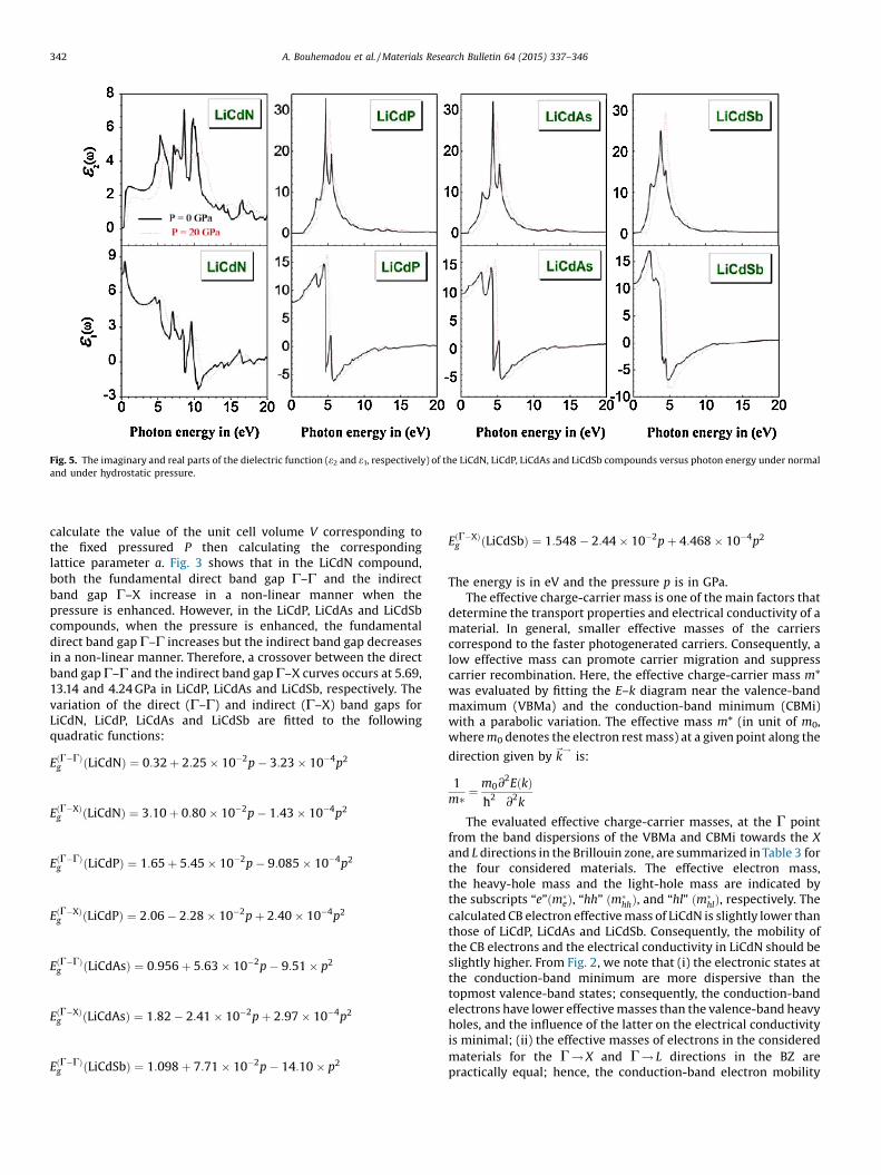
Fig. 5. The imaginary and real parts of the dielectric function (e2 and e1, respectively) of the LiCdN, LiCdP, LiCdAs and LiCdSb compounds versus photon energy under normaland under hydrostatic pressure.
342 A. Bouhemadou et al. /Materials Research Bulletin 64 (2015) 337–346
and the electrical conductivity of the studied materials should beisotropic; (iii) the heavy holes have higher effective masses thanthe light holes, which indicates the anisotropy between heavy- andlight-hole masses; and (iv) the dependence of the effective massesof the heavy holes on the crystallographic direction demonstratesthe anisotropy of this property; hence, the valence-band heavyhole conductivity should also be anisotropic.
To understand the nature of the band structures in theinvestigated compounds, orbital-resolved partial densities of
states (PDOSs) spectra calculated using TB–mBJ functional arepresented in Fig. 4. The calculated DOS spectra show similaritiesfor the four investigated materials. The first group of valencebands, if we start from lower energies, reflects the group V atom(i.e., N, P, As and Sb) s states. The second one consists of the Cd dstates with small contributions from the column V atom s and pstates; the contribution of the s states increases in this sequence,LiCdN! LiCdP! LiCdAs! LiCdSb, whereas the contribution of thep states decreases following that sequence. The rest of the valence
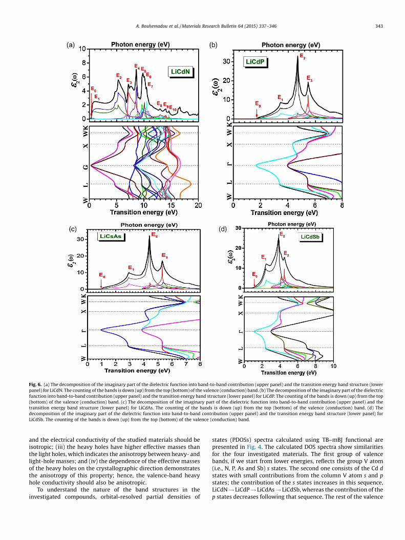
[(Fig._6)TD$FIG]
Fig. 6. (a) The decomposition of the imaginary part of the dielectric function into band-to-band contribution (upper panel) and the transition energy band structure (lowerpanel) for LiCdN. The counting of the bands is down (up) from the top (bottom) of the valence (conduction) band. (b) The decomposition of the imaginary part of the dielectricfunction into band-to-band contribution (upper panel) and the transition energy band structure (lower panel) for LiCdP. The counting of the bands is down (up) from the top(bottom) of the valence (conduction) band. (c) The decomposition of the imaginary part of the dielectric function into band-to-band contribution (upper panel) and thetransition energy band structure (lower panel) for LiCdAs. The counting of the bands is down (up) from the top (bottom) of the valence (conduction) band. (d) Thedecomposition of the imaginary part of the dielectric function into band-to-band contribution (upper panel) and the transition energy band structure (lower panel) forLiCdSb. The counting of the bands is down (up) from the top (bottom) of the valence (conduction) band.
A. Bouhemadou et al. /Materials Research Bulletin 64 (2015) 337–346 343
and conduction bands are mixture of s and p states of theconstituent elements with small contributions from the d statesatoms.
3.3. Optical properties
The calculated imaginary parts e2(v) of the frequency-dependent dielectric function for the four considered materialsbased on the band results discussed in the preceding section areshown in Fig. 5. The behavior of e2(v) is rather similar for the LiCdP,LiCdAs and LiCdSb compounds with some differences in details.
The e2(v) spectrum of the LiCdN compound is quite different fromthe three others; it is too broad and contains more structures thanthose of LiCdP, LiCdAs and LiCdSb.
It is worthwhile to attempt to identify the microscopic origin ofthe transitions that are responsible for the peaks and features ine2(v). The imaginary part of the dielectric function is determinedby the allowed direct electronic transitions between each pair ofoccupied and unoccupied bands. Therefore, the origins of different
Table 6Peak positions of the e2(v) spectrum together with the dominant interbandtransition contributions to every peak and their location in the Brillouin zone ofLiCdP.
Optical structures Dominant interband transition contributions
Structure Peak position Transition Region Energy (eV)
E0 1.65 (V1–C1) Γ–Γ 1.65
E1 3.447 (V1–C1) W–L, G–X 3.44(V2–C1) W–L, G–X 3.44
E2 4.688 (V1–C1) W–L, X–W–K 4.69(V1–C2) L–G–X 4.69(V2–C1) W–L, X–W 4.66
E3 5.46 (V1–C2) L–G–X 5.40(V1–C3) W–L, G–X 5.51(V1–C4) L–G–X 5.23(V2–C2) W–L, X–W 5.51(V2–C3) W–L, G–X 5.59
Table 5Peak positions of the e2(v) spectrum together with the dominant interbandtransition contributions to every peak and their location in the Brillouin zone ofLiCdN.
Optical structures Dominant interband transition contributions
Structure Peak position Transition Region Energy (eV)
E0 0.32 (V1–C1) Γ–Γ 0.32
E1 0.90 (V1–C1) L–G–X 1.33(V2–C1) L–G–X 0.80(V3–C1) L–G–X 0.6
E2 5.32 (V1–C1) W–L, X–W 5.25(V2–C1) W–L, G–X–W 4.71, 5.26
E3 7.17 (V1–C2) W–L 7.14(V3–C1) L–G, X–W 6.64
E4 8.60 (V1–C2) W–L, G–X, W–K 8.49(V2–C2) W–L, G–X 8.64(V3–C1) W–L, X–W–K 8.43
E4 9.81 (V1–C3) W–L–G–X 9.58(V1–C4) W–L, G–X 9.64(V2–C3) L–G–X 9.58(V2–C4) W–L, G–X 9.89
E5 10.08 (V2–C4) W–L, G–X 9.89(V3–C2) W–L–G–X 10.12
E6 10.50 (V1–C4) W–L, G–X 10.73(V2–C3) W–L, G–X–W–K 10.44
E7 12.93 (V1–C5) G–X–W 12.95(V2–C5) G–X–W 13.07(V3–C3) W–L–G–X–W–K 11.92(V4–C1) W–L, X–W–K 12.34(V7–C1) W–L, X–W 12.13(V8–C1) W–L, X–W 12.13
E8 13.93 (V1–C5) L–G–X–W–K 14.03(V3–C4) W–L, W–K 14.03(V3–C5) G–X 13.61(V4–C2) W–L 13.17
E9 14.58 (V5–C2) W–L–G, W–K 14.34(V6–C2) W–L–G–X–W–K 14.55(V7–C2) W–L, G–X–W–K 14.55(V8–C2) W–L, W–K 14.6
Table 4Calculated static dielectric constant e1(0) and static refractive index of the LiCdN,LiCdP, LiCdAs and LiCdSb compounds compared with the available literature.
LiCdN LiCdP LiCdAs LiCdSb
e(0) 7.52 7.88 9.32 10.936.898 [38] 7.568 [38] 8.09 [38]
12.205 [34] 15.46 [35]
n(0) 2.742 2.808 3.053 3.3072.626 [38] 2.751 [38] 2.844 [38]
3.4936 [34] 3.932 [35]
Table 7Peak positions of the e2(v) spectrum together with the dominant interbandtransition contributions to every peak and their location in the Brillouin zone ofLiCdAs.
Optical structures Dominant interband transition contributions
Structure Peak position Transition Region Energy (eV)
E0 0.96 (V1–C1) Γ–Γ 0.96
E1 2.930 (V1–C1) W–L, G–X 2.94(V2–C1) W–L, G–X 2.97
E2 4.390 (V1–C1) W–L, G–X–W 4.42(V1–C2) L–G–X 4.46(V2–C1) W–L, G–X–W 4.34(V2–C2) W–L, X–W 4.50
E3 5.30 (V1–C2) W–L–G, X–W 5.30(V1–C3) W–L, G–X 5.36(V2–C2) W–L–G, X–W 5.11, 5.32
Table 8Peak positions of the e2(v) spectrum together with the dominant interbandtransition contributions to every peak and their location in the Brillouin zone ofLiCdSb.
Optical structures Dominant interband transition contributions
Structure Peak position Transition Region Energy (eV)
E0 1.10 (V1–C1) Γ–Γ 1.10
E1 2.46 (V1–C1) W–L, G–X 2.459(V2-C1) W–L, G–X 2.46
E2 3.84 (V1–C1) W–L, X–W–K 3.88(V1–C4) L–G–X 3.54(V2–C1) W–L, X–W 3.88
E3 4.48 (V1–C2) W–L–G–X–W 4.10, 4.56(V1–C3) W–L, G–X 4.52(V1–C4) L–G–X 4.75(V2–C2) W–L–G, X–W 4.23, 4.50(V2–C3) W–L, G–X 4.527
344 A. Bouhemadou et al. /Materials Research Bulletin 64 (2015) 337–346
structures of the optical spectra can be determined by decom-posing each spectrum into its individual pair contribution, i.e., thecontribution from each direct electronic transition from theoccupied valence state Vi to the empty conduction state Cj(Vi!Cj).This technique informs us about the bands that contribute more tothe peaks of the e2(v) spectrum. In order to determine thelocations in the BZ of the electronic states that are involved in thesetransitions, the electronic transition energy Eij(k) = ECj(k)� EVi(k)are plotted along the high-symmetry directions in the BZ. In Fig. 6a, b, c and d, the top panel shows the dominant contributions to
e2(v) from the interband transitions, and the bottom panel showsthe locations of these transitions in the BZ for the four consideredmaterials. The first critical point E0 of e2(v) is the edge of theoptical absorption. This point is the ΓV–ΓC splitting, which givesthe threshold of the direct optical transition between the topmostvalence band V1 and the bottommost conduction band C1(V1!C1)(transition); the counting of the bands is down (up) from the top(bottom) of the valence (conduction) band. This edge is known asthe fundamental absorption edge. This first critical point isfollowed by a number of structures Ei. The locations of the majorpeaks Ei with the dominant contributions from the interbandtransitions to each peak and their locations in the Brillouin zone forall four compounds are reported in Tables 5–8.
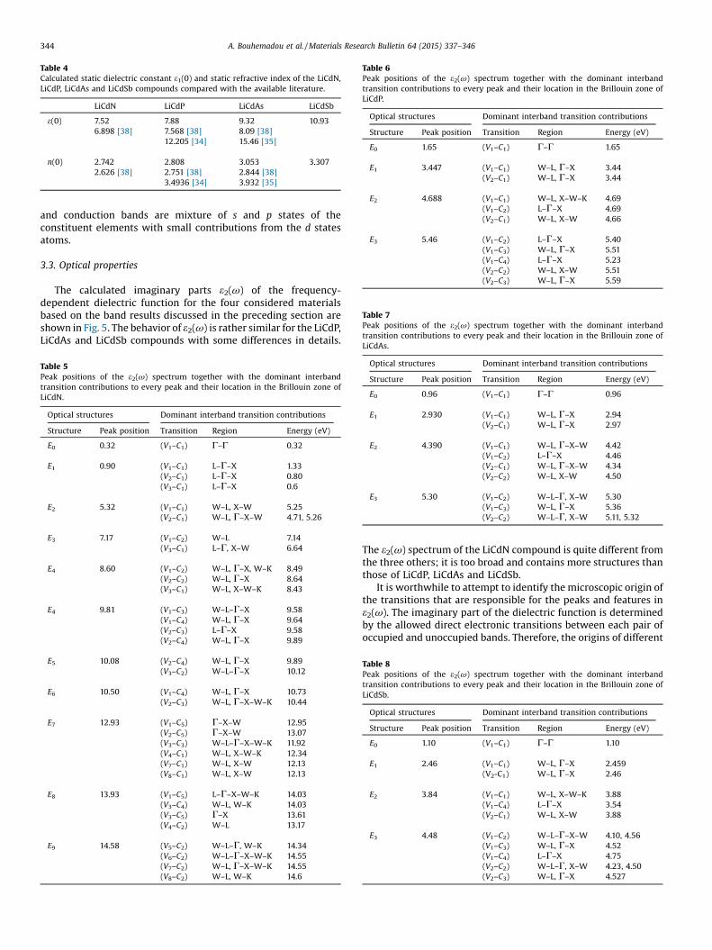
The results for the dispersive part of the dielectric function,e1(v) for the four consideredmaterials are given in Fig. 5. Themainfeatures in the e1(v) curves of LiCdP, LiCdAs and LiCdSb are: a peakat around 4 eV; an abrupt decrease to the zero value, after whiche1(v) becomes negative, a minimum at about 6 eV, followed by aslow increase toward zero. The static dielectric constant e1(0) isgiven by the low energy limit of e1(v). The calculated staticdielectric constants e1(0) for the studied materials are listed inTable 4 in comparison with the available theoretical results. Ourcalculated values of e1(0) agree rather well with those previouslycalculated by Mehnane et al. [38] using the full-potential (linear)augmented plane wave plus local orbitals (L/APW+ lo) with thestandard GGA–PBE [61], but they are somewhat smaller comparedto those reported in Ref. [34] using pseudopotential plane wavemethod. The value of e1(0) increases with the increase of theatomic number of the group V elements. In addition, Fig. 7 showsthe pressure dependence of e1(0). For all the consideredcompounds, we have got negative values for de1(0)/dp, which isnearly 0 for LiCdP.
[(Fig._7)TD$FIG]
Fig. 7. Variation of the static dielectric function e(0) as a function of pressure for theLiCdN, LiCdP, LiCdAs and LiCdSb compounds.
[(Fig._8)TD$FIG]
Fig. 8. Calculated absorption coefficient, refractive index, extinction coefficient, reflectivity and energy-loss function spectra of the LiCdN, LiCdP, LiCdAs and LiCdSbcompounds as calculated using the TB–mBJ potential.
A. Bouhemadou et al. /Materials Research Bulletin 64 (2015) 337–346 345
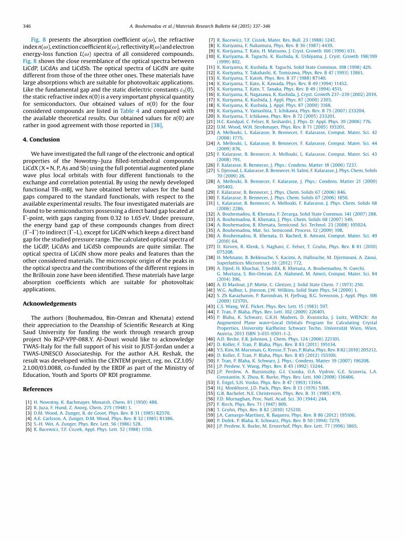
Fig. 8 presents the absorption coefficient a(v), the refractiveindexn(v), extinctioncoefficientk(v), reflectivityR(v)andelectronenergy-loss function L(v) spectra of all considered compounds.Fig. 8 shows the close resemblance of the optical spectra betweenLiCdP, LiCdAs and LiCdSb. The optical spectra of LiCdN are quitedifferent from those of the three other ones. These materials havelarge absorptions which are suitable for photovoltaic applications.Like the fundamental gap and the static dielectric constants e1(0),the static refractive index n(0) is a very important physical quantityfor semiconductors. Our obtained values of n(0) for the fourconsidered compounds are listed in Table 4 and compared withthe available theoretical results. Our obtained values for n(0) arerather in good agreement with those reported in [38].
4. Conclusion
Wehave investigated the full range of the electronic and opticalproperties of the Nowotny–Juza filled-tetrahedral compoundsLiCdX (X=N, P, As and Sb) using the full potential augmented planewave plus local orbitals with four different functionals to theexchange and correlation potential. By using the newly developedfunctional TB–mBJ, we have obtained better values for the bandgaps compared to the standard functionals, with respect to theavailable experimental results. The four investigated materials arefound to be semiconductors possessing a direct band gap located atΓ-point, with gaps ranging from 0.32 to 1.65 eV. Under pressure,the energy band gap of these compounds changes from direct(Γ–Γ) to indirect (Γ–L), except for LiCdNwhich keeps a direct bandgap for the studied pressure range. The calculated optical spectra ofthe LiCdP, LiCdAs and LiCdSb compounds are quite similar. Theoptical spectra of LiCdN show more peaks and features than theother considered materials. The microscopic origin of the peaks inthe optical spectra and the contributions of the different regions inthe Brillouin zone have been identified. These materials have largeabsorption coefficients which are suitable for photovoltaicapplications.
Acknowledgements
The authors (Bouhemadou, Bin-Omran and Khenata) extendtheir appreciation to the Deanship of Scientific Research at KingSaud University for funding the work through research groupproject No RGP-VPP-088.Y. Al-Douri would like to acknowledgeTWAS-Italy for the full support of his visit to JUST-Jordan under aTWAS-UNESCO Associateship. For the author A.H. Reshak, theresult was developed within the CENTEM project, reg. no. CZ.1.05/2.1.00/03.0088, co-funded by the ERDF as part of the Ministry ofEducation, Youth and Sports OP RDI programme.
References
[1] H. Nowotny, K. Bachmayer, Monatsh. Chem. 81 (1950) 488.[2] R. Juza, F. Hund, Z. Anorg. Chem. 275 (1948) 1.[3] D.M. Wood, A. Zunger, R. de Groot, Phys. Rev. B 31 (1985) R2570.[4] A.E. Carlsson, A. Zunger, D.M. Wood, Phys. Rev. B 32 (1985) R1386.[5] S.-H. Wei, A. Zunger, Phys. Rev. Lett. 56 (1986) 528.[6] R. Bacewicz, T.F. Ciszek, Appl. Phys. Lett. 52 (1988) 1150.
[7] R. Bacewicz, T.F. Ciszek, Mater. Res. Bull. 23 (1988) 1247.[8] K. Kuriyama, F. Nakamura, Phys. Rev. B 36 (1987) 4439.[9] K. Kuriyama, T. Kato, H. Matsuno, J. Cryst. Growth 166 (1996) 631.
[10] K. Kuriyama, R. Taguchi, K. Kushida, K. Ushiyama, J. Cryst. Growth 198/199(1999) 802.
[11] K. Kuriyama, K. Kushida, R. Taguchi, Solid State Commun. 108 (1998) 429.[12] K. Kuriyama, Y. Takahashi, K. Tomizawa, Phys. Rev. B 47 (1993) 13861.[13] K. Kuriyama, T. Katoh, Phys. Rev. B 37 (1988) R7140.[14] K. Kuriyama, T. Kato, K. Kawada, Phys. Rev. B 49 (1994) 11452.[15] K. Kuriyama, T. Kato, T. Tanaka, Phys. Rev. B 49 (1994) 4511.[16] K. Kuriyama, K. Nagasawa, K. Kushida, J. Cryst. Growth 237–239 (2002) 2019.[17] K. Kuriyama, K. Kushida, J. Appl. Phys. 87 (2000) 2303.[18] K. Kuriyama, K. Kushida, J. Appl. Phys. 87 (2000) 3168.[19] K. Kuriyama, Y. Yamashita, T. Ichikawa, Phys. Rev. B 75 (2007) 233204.[20] K. Kuriyama, T. Ichikawa, Phys. Rev. B 72 (2005) 233201.[21] H.C. Kandpal, C. Felser, R. Seshardri, J. Phys. D: Appl. Phys. 39 (2006) 776.[22] D.M. Wood, W.H. Strohmayer, Phys. Rev. B 71 (2005) 193201.[23] A. Mellouki, L. Kalarasse, B. Bennecer, F. Kalarasse, Comput. Mater. Sci. 42
(2008) 1775.[24] A. Mellouki, L. Kalarasse, B. Bennecer, F. Kalarasse, Comput. Mater. Sci. 44
(2009) 876.[25] F. Kalarasse, B. Bennecer, A. Mellouki, L. Kalarasse, Comput. Mater. Sci. 43
(2008) 791.[26] F. Kalarasse, B. Bennecer, J. Phys.: Condens. Matter 18 (2006) 7237.[27] S. Djeroud, L. Kalarasse, B. Bennecer, H. Salmi, F. Kalarasse, J. Phys. Chem. Solids
70 (2009) 26.[28] A. Mellouki, B. Bennecer, F. Kalarasse, J. Phys.: Condens. Matter 21 (2009)
305402.[29] F. Kalarasse, B. Bennecer, J. Phys. Chem. Solids 67 (2006) 846.[30] F. Kalarasse, B. Bennecer, J. Phys. Chem. Solids 67 (2006) 1850.[31] L. Kalarasse, B. Bennecer, A. Mellouki, F. Kalarasse, J. Phys. Chem. Solids 68
(2006) 2286.[32] A. Bouhemadou, R. Khenata, F. Zerarga, Solid State Commun. 141 (2007) 288.[33] A. Bouhemadou, R. Khenata, J. Phys. Chem. Solids 68 (2007) 549.[34] A. Bouhemadou, R. Khenata, Semicond. Sci. Technol. 23 (2008) 105024.[35] A. Bouhemadou, Mat. Sci. Semicond. Process. 12 (2009) 198.[36] A. Bouhemadou, R. Khenata, D. Rached, B. Amrani, Comput. Mater. Sci. 49
(2010) 64.[37] D. Kieven, R. Klenk, S. Naghavi, C. Felser, T. Gruhn, Phys. Rev. B 81 (2010)
075208.[38] H. Mehnane, B. Bekkouche, S. Kacimi, A. Hallouche, M. Djermouni, A. Zaoui,
Superlattices Microstruct. 51 (2012) 772.[39] A. Djied, H. Khachai, T. Seddik, R. Khenata, A. Bouhemadou, N. Guechi,
G. Murtaza, S. Bin-Omran, Z.A. Alahmed, M. Ameri, Comput. Mater. Sci. 84(2014) 396.
[40] A. El Maslout, J.P. Motte, C. Gleitzer, J. Solid State Chem. 7 (1973) 250.[41] W.G. Aulbur, L. Jönsson, J.W. Wilkins, Solid State Phys. 54 (2000) 1.[42] S. Zh Karazhanov, P. Ravindran, H. Fjellvag, B.G. Svensson, J. Appl. Phys. 106
(2009) 123701.[43] C.S. Wang, W.E. Picket, Phys. Rev. Lett. 15 (1983) 597.[44] F. Tran, P. Blaha, Phys. Rev. Lett. 102 (2009) 226401.[45] P. Blaha, K. Schwarz, G.K.H. Madsen, D. Kvasnicka, J. Luitz, WIEN2k: An
Augmented Plane wave+Local Orbitals Program for Calculating CrystalProperties, University Karlheinz Schwarz Techn. Universität Wien, Wien,Austria, 2013 ISBN 3-031-9501-1-2.
[46] A.D. Becke, E.R. Johnson, J. Chem. Phys. 124 (2006) 221101.[47] D. Koller, F. Tran, P. Blaha, Phys. Rev. B 83 (2011) 195134.[48] Y.S. Kim,M.Marsman, G. Kresse, F. Tran, P. Blaha, Phys. Rev. B 82 (2010) 205212.[49] D. Koller, F. Tran, P. Blaha, Phys. Rev. B 85 (2012) 155109.[50] F. Tran, P. Blaha, K. Schwarz, J. Phys.: Condens. Matter 19 (2007) 196208.[51] J.P. Perdew, Y. Wang, Phys. Rev. B 45 (1992) 13244.[52] J.P. Perdew, A. Ruzsinszky, G.I. Csonka, O.A. Vydrov, G.E. Scuseria, L.A.
Constantin, X. Zhou, K. Burke, Phys. Rev. Lett. 100 (2008) 136406.[53] E. Engel, S.H. Vosko, Phys. Rev. B 47 (1993) 13164.[54] H.J. Monkhorst, J.D. Pack, Phys. Rev. B 13 (1976) 5188.[55] G.B. Bachelet, N.E. Christensen, Phys. Rev. B. 31 (1985) 879.[56] F.D. Murnaghan, Proc. Natl. Acad. Sci. 30 (1944) 244.[57] F. Birch, Phys. Rev. 71 (1947) 809.[58] T. Gruhn, Phys. Rev. B 82 (2010) 125210.[59] J.A. Camargo-Martínez, R. Baquero, Phys. Rev. B 86 (2012) 195106.[60] P. Dufek, P. Blaha, K. Schwarz, Phys. Rev. B 50 (1994) 7279.[61] J.P. Perdew, K. Burke, M. Ernzerhof, Phys. Rev. Lett. 77 (1996) 3865.
346 A. Bouhemadou et al. /Materials Research Bulletin 64 (2015) 337–346
![Assessment of the GLLB-SC potential for solid-state ... · Becke-Johnson (mBJ) potential [Tran and Blaha, Phys.Rev.Lett.102, 226401 (2009)], for electronic, magnetic, and density-related](https://img.pdfslide.net/doc/110x75/60444c5e22758b4a6b256290/assessment-of-the-gllb-sc-potential-for-solid-state-becke-johnson-mbj-potential.jpg)