Embed Size (px)
Citation preview
Materials Science and Engineering R 68 (2010) 89–133
Advances in the growth and characterization of magnetic, ferroelectric, andmultiferroic oxide thin films
L.W. Martin a,b,*, Y.-H. Chu c, R. Ramesh d,e,f
a Department of Materials Science and Engineering, University of Illinois, Urbana-Champaign, Urbana, IL 61801, USAb Frederick Seitz Materials Research Laboratory, University of Illinois, Urbana-Champaign, Urbana, IL 61801, USAc Department of Materials Science and Engineering, National Chiao Tung University, HsinChu 30100, Taiwand Department of Materials Science and Engineering University of California, Berkeley, Berkeley, CA 94720, USAe Department of Physics, University of California, Berkeley, Berkeley, CA 94720, USAf Materials Science Division, Lawrence Berkeley National Laboratory, Berkeley, CA 94720, USA
Contents
1. Introduction . . . . . . . . . . . . . . . . . . . . . . . . . . . . . . . . . . . . . . . . . . . . . . . . . . . . . . . . . . . . . . . . . . . . . . . . . . . . . . . . . . . . . . . . . . . . . . . . . . . . . . 90
2. The wide-world of complex oxides: structures and chemistry . . . . . . . . . . . . . . . . . . . . . . . . . . . . . . . . . . . . . . . . . . . . . . . . . . . . . . . . . . . . . . 90
3. Advances in the growth of oxide thin films . . . . . . . . . . . . . . . . . . . . . . . . . . . . . . . . . . . . . . . . . . . . . . . . . . . . . . . . . . . . . . . . . . . . . . . . . . . . . 92
3.1. Thin film growth modes and epitaxy. . . . . . . . . . . . . . . . . . . . . . . . . . . . . . . . . . . . . . . . . . . . . . . . . . . . . . . . . . . . . . . . . . . . . . . . . . . . . 92
3.2. Pulsed-laser ablation-based techniques . . . . . . . . . . . . . . . . . . . . . . . . . . . . . . . . . . . . . . . . . . . . . . . . . . . . . . . . . . . . . . . . . . . . . . . . . . . 94
3.2.1. Laser-material interactions . . . . . . . . . . . . . . . . . . . . . . . . . . . . . . . . . . . . . . . . . . . . . . . . . . . . . . . . . . . . . . . . . . . . . . . . . . . . . 95
3.2.2. Recent advances in pulsed laser deposition . . . . . . . . . . . . . . . . . . . . . . . . . . . . . . . . . . . . . . . . . . . . . . . . . . . . . . . . . . . . . . . . 96
3.3. Molecular beam epitaxy . . . . . . . . . . . . . . . . . . . . . . . . . . . . . . . . . . . . . . . . . . . . . . . . . . . . . . . . . . . . . . . . . . . . . . . . . . . . . . . . . . . . . . . 97
3.4. Sputtering . . . . . . . . . . . . . . . . . . . . . . . . . . . . . . . . . . . . . . . . . . . . . . . . . . . . . . . . . . . . . . . . . . . . . . . . . . . . . . . . . . . . . . . . . . . . . . . . . . 97
3.5. Metal-organic chemical vapor deposition . . . . . . . . . . . . . . . . . . . . . . . . . . . . . . . . . . . . . . . . . . . . . . . . . . . . . . . . . . . . . . . . . . . . . . . . . 97
3.6. Solution-based thin film deposition techniques . . . . . . . . . . . . . . . . . . . . . . . . . . . . . . . . . . . . . . . . . . . . . . . . . . . . . . . . . . . . . . . . . . . . 97
3.7. Low-temperature aqueous solution depositions . . . . . . . . . . . . . . . . . . . . . . . . . . . . . . . . . . . . . . . . . . . . . . . . . . . . . . . . . . . . . . . . . . . . 98
A R T I C L E I N F O
Article history:
Received 22 March 2010
Accepted 24 March 2010
Available online 21 April 2010
Keywords:
Thin films
Multiferroic
Magnetic
ferroelectric
Complex oxides
A B S T R A C T
The growth and characterization of functional oxide thin films that are ferroelectric, magnetic, or both at
the same time are reviewed. The evolution of synthesis techniques and how advances in in situ
characterization have enabled significant acceleration in improvements to these materials are described.
Methods for enhancing the properties of functional materials or creating entirely new functionality at
interfaces are covered, including strain engineering and layering control at the atomic-layer level.
Emerging applications of these functional oxides such as achieving electrical control of ferromagnetism
and the future of these complex functional oxides is discussed.
� 2010 Elsevier B.V. All rights reserved.
Abbreviations: AAO, anodized aluminum oxide; AF, antiferromagnet; AFM, atomic force microscopy; BFO, BiFeO3; BMO, BiMnO3; BTO, BaTiO3; c-AFM, conducting atomic
force microscopy; CBD, chemical bath deposition; CFO, CoFe2O4; CMR, colossal magnetoresistance; CSD, chemical solution deposition; DSO, DyScO3; EB, exchange bias; ED,
electroless deposition; eV, electron volt; FeRAM, ferroelectric random access memory; FM, ferromagnet; GMR, giant magnetoresistance; GSO, GdScO3; H, magnetic field;
HRTEM, high-resolution transmission electron microscopy; LSMO, La0.7Ca0.3MnO3; LPD, liquid phase deposition; LSAT, (LaAlO3)0.29–(Sr0.5Al0.5TaO3)0.71; MBE, molecular beam
epitaxy; MOCVD, metal-organic chemical vapor deposition; MRAM, magnetic random access memory; Oe, Oersted; PS, saturation polarization; P–E, polarization–electric
field; PCD, photochemical deposition; PEEM, photoemission electron microscopy; PFM, piezoresponse force microscopy; PLD, pulsed laser deposition; PMN-PT,
Pb(Mg0.33Nb0.67)O3–PbTiO3; PTO, PbTiO3; PZT, Pb(Zrx,Ti1�x)O3; RF, radio-frequency; RHEED, reflection high-energy electron diffraction; RHEED-TRAXS, reflection high-
energy electron diffraction total reflection angle X-ray spectroscopy; SBT, SrBi2Ta2O9; SPES, spin-resolved photoemission spectroscopy; SQUID, superconducting quantum
Contents lists available at ScienceDirect
Materials Science and Engineering R
journa l homepage: www.e lsev ier .com/ locate /mser
interference device; SRO, SrRuO3; STO, SrTiO3; TC, Curie temperature; TN, Neel temperature; TEM, transmission electron microscopy; TMR, tunnel magnetoresistance; ToF-
ISARS, time-of-flight ion scattering and recoil spectroscopy; XMCD, X-ray magnetic circular dichroism; YMO, YMnO3.
* Corresponding author at: Department of Materials Science and Engineering, University of Illinois, Urbana-Champaign, Urbana, IL 61801, USA. Tel.: +1 217 244 9162;
fax: +1 217 333 2736.
E-mail address: [email protected] (L.W. Martin).
0927-796X/$ – see front matter � 2010 Elsevier B.V. All rights reserved.
doi:10.1016/j.mser.2010.03.001
L.W. Martin et al. / Materials Science and Engineering R 68 (2010) 89–13390
4. Ferroelectricity in oxides . . . . . . . . . . . . . . . . . . . . . . . . . . . . . . . . . . . . . . . . . . . . . . . . . . . . . . . . . . . . . . . . . . . . . . . . . . . . . . . . . . . . . . . . . . . . 98
4.1. Definition of ferroelectric materials . . . . . . . . . . . . . . . . . . . . . . . . . . . . . . . . . . . . . . . . . . . . . . . . . . . . . . . . . . . . . . . . . . . . . . . . . . . . . . 98
4.2. Brief history of ferroelectrics . . . . . . . . . . . . . . . . . . . . . . . . . . . . . . . . . . . . . . . . . . . . . . . . . . . . . . . . . . . . . . . . . . . . . . . . . . . . . . . . . . . 98
4.3. Thin film ferroelectric phenomena. . . . . . . . . . . . . . . . . . . . . . . . . . . . . . . . . . . . . . . . . . . . . . . . . . . . . . . . . . . . . . . . . . . . . . . . . . . . . . . 99
4.3.1. Size effects in ferroelectrics . . . . . . . . . . . . . . . . . . . . . . . . . . . . . . . . . . . . . . . . . . . . . . . . . . . . . . . . . . . . . . . . . . . . . . . . . . . . 99
4.3.2. Strain effects in ferroelectricity. . . . . . . . . . . . . . . . . . . . . . . . . . . . . . . . . . . . . . . . . . . . . . . . . . . . . . . . . . . . . . . . . . . . . . . . . 100
4.3.3. Artificially engineered ferroelectrics . . . . . . . . . . . . . . . . . . . . . . . . . . . . . . . . . . . . . . . . . . . . . . . . . . . . . . . . . . . . . . . . . . . . . 102
4.3.4. Controlling ferroelectric domain structures . . . . . . . . . . . . . . . . . . . . . . . . . . . . . . . . . . . . . . . . . . . . . . . . . . . . . . . . . . . . . . . 103
4.4. Ferroelectric devices and integration . . . . . . . . . . . . . . . . . . . . . . . . . . . . . . . . . . . . . . . . . . . . . . . . . . . . . . . . . . . . . . . . . . . . . . . . . . . . 105
4.5. Ferroelectric tunnel junctions and novel transport phenomena. . . . . . . . . . . . . . . . . . . . . . . . . . . . . . . . . . . . . . . . . . . . . . . . . . . . . . . 106
5. Magnetism in oxides . . . . . . . . . . . . . . . . . . . . . . . . . . . . . . . . . . . . . . . . . . . . . . . . . . . . . . . . . . . . . . . . . . . . . . . . . . . . . . . . . . . . . . . . . . . . . . 106
5.1. Definition of magnetic materials . . . . . . . . . . . . . . . . . . . . . . . . . . . . . . . . . . . . . . . . . . . . . . . . . . . . . . . . . . . . . . . . . . . . . . . . . . . . . . . 106
5.2. Brief history of magnetic oxides . . . . . . . . . . . . . . . . . . . . . . . . . . . . . . . . . . . . . . . . . . . . . . . . . . . . . . . . . . . . . . . . . . . . . . . . . . . . . . . 107
5.3. Common types of magnetism in transition metal oxides . . . . . . . . . . . . . . . . . . . . . . . . . . . . . . . . . . . . . . . . . . . . . . . . . . . . . . . . . . . . 107
5.3.1. Superexchange. . . . . . . . . . . . . . . . . . . . . . . . . . . . . . . . . . . . . . . . . . . . . . . . . . . . . . . . . . . . . . . . . . . . . . . . . . . . . . . . . . . . . . 107
5.3.2. Double exchange . . . . . . . . . . . . . . . . . . . . . . . . . . . . . . . . . . . . . . . . . . . . . . . . . . . . . . . . . . . . . . . . . . . . . . . . . . . . . . . . . . . . 108
5.3.3. RKKY coupling . . . . . . . . . . . . . . . . . . . . . . . . . . . . . . . . . . . . . . . . . . . . . . . . . . . . . . . . . . . . . . . . . . . . . . . . . . . . . . . . . . . . . . 108
5.4. Modern magnetic oxides . . . . . . . . . . . . . . . . . . . . . . . . . . . . . . . . . . . . . . . . . . . . . . . . . . . . . . . . . . . . . . . . . . . . . . . . . . . . . . . . . . . . . 108
5.4.1. Ferrites . . . . . . . . . . . . . . . . . . . . . . . . . . . . . . . . . . . . . . . . . . . . . . . . . . . . . . . . . . . . . . . . . . . . . . . . . . . . . . . . . . . . . . . . . . . . 108
5.4.2. Manganites . . . . . . . . . . . . . . . . . . . . . . . . . . . . . . . . . . . . . . . . . . . . . . . . . . . . . . . . . . . . . . . . . . . . . . . . . . . . . . . . . . . . . . . . 109
5.5. Thin film magnetic phenomena . . . . . . . . . . . . . . . . . . . . . . . . . . . . . . . . . . . . . . . . . . . . . . . . . . . . . . . . . . . . . . . . . . . . . . . . . . . . . . . . 110
5.5.1. Superlattice effects . . . . . . . . . . . . . . . . . . . . . . . . . . . . . . . . . . . . . . . . . . . . . . . . . . . . . . . . . . . . . . . . . . . . . . . . . . . . . . . . . . 110
5.5.2. Exchange coupling across interfaces. . . . . . . . . . . . . . . . . . . . . . . . . . . . . . . . . . . . . . . . . . . . . . . . . . . . . . . . . . . . . . . . . . . . . 111
6. Multiferroism and magnetoelectricity . . . . . . . . . . . . . . . . . . . . . . . . . . . . . . . . . . . . . . . . . . . . . . . . . . . . . . . . . . . . . . . . . . . . . . . . . . . . . . . . 112
6.1. Scarcity of multiferroics . . . . . . . . . . . . . . . . . . . . . . . . . . . . . . . . . . . . . . . . . . . . . . . . . . . . . . . . . . . . . . . . . . . . . . . . . . . . . . . . . . . . . . 112
6.2. Pathways to multiferroism . . . . . . . . . . . . . . . . . . . . . . . . . . . . . . . . . . . . . . . . . . . . . . . . . . . . . . . . . . . . . . . . . . . . . . . . . . . . . . . . . . . . 113
6.3. Definition of magnetoelectricity. . . . . . . . . . . . . . . . . . . . . . . . . . . . . . . . . . . . . . . . . . . . . . . . . . . . . . . . . . . . . . . . . . . . . . . . . . . . . . . . 113
6.4. Thin film multiferroics . . . . . . . . . . . . . . . . . . . . . . . . . . . . . . . . . . . . . . . . . . . . . . . . . . . . . . . . . . . . . . . . . . . . . . . . . . . . . . . . . . . . . . . 113
6.4.1. Manganite multiferroic thin films. . . . . . . . . . . . . . . . . . . . . . . . . . . . . . . . . . . . . . . . . . . . . . . . . . . . . . . . . . . . . . . . . . . . . . . 113
6.4.2. BiMnO3 thin films . . . . . . . . . . . . . . . . . . . . . . . . . . . . . . . . . . . . . . . . . . . . . . . . . . . . . . . . . . . . . . . . . . . . . . . . . . . . . . . . . . . 114
6.4.3. BiFeO3 thin films . . . . . . . . . . . . . . . . . . . . . . . . . . . . . . . . . . . . . . . . . . . . . . . . . . . . . . . . . . . . . . . . . . . . . . . . . . . . . . . . . . . . 115
6.4.4. Other single phase multiferroic thin films . . . . . . . . . . . . . . . . . . . . . . . . . . . . . . . . . . . . . . . . . . . . . . . . . . . . . . . . . . . . . . . . 119
6.4.5. Horizontal multilayer heterostructures . . . . . . . . . . . . . . . . . . . . . . . . . . . . . . . . . . . . . . . . . . . . . . . . . . . . . . . . . . . . . . . . . . 119
6.4.6. Vertical nanostructures . . . . . . . . . . . . . . . . . . . . . . . . . . . . . . . . . . . . . . . . . . . . . . . . . . . . . . . . . . . . . . . . . . . . . . . . . . . . . . . 121
6.5. Engineering new functionalities with multiferroics . . . . . . . . . . . . . . . . . . . . . . . . . . . . . . . . . . . . . . . . . . . . . . . . . . . . . . . . . . . . . . . . 122
6.5.1. Electric field versus current control of magnetism . . . . . . . . . . . . . . . . . . . . . . . . . . . . . . . . . . . . . . . . . . . . . . . . . . . . . . . . . 122
6.5.2. Electric field control of ferromagnetism . . . . . . . . . . . . . . . . . . . . . . . . . . . . . . . . . . . . . . . . . . . . . . . . . . . . . . . . . . . . . . . . . . 123
6.5.3. Exchange bias with multiferroic antiferromagnets . . . . . . . . . . . . . . . . . . . . . . . . . . . . . . . . . . . . . . . . . . . . . . . . . . . . . . . . . 124
6.6. Advanced multiferroic-based devices . . . . . . . . . . . . . . . . . . . . . . . . . . . . . . . . . . . . . . . . . . . . . . . . . . . . . . . . . . . . . . . . . . . . . . . . . . . 126
7. Future directions and conclusions . . . . . . . . . . . . . . . . . . . . . . . . . . . . . . . . . . . . . . . . . . . . . . . . . . . . . . . . . . . . . . . . . . . . . . . . . . . . . . . . . . . 128
Acknowledgements . . . . . . . . . . . . . . . . . . . . . . . . . . . . . . . . . . . . . . . . . . . . . . . . . . . . . . . . . . . . . . . . . . . . . . . . . . . . . . . . . . . . . . . . . . . . . . . 129
References . . . . . . . . . . . . . . . . . . . . . . . . . . . . . . . . . . . . . . . . . . . . . . . . . . . . . . . . . . . . . . . . . . . . . . . . . . . . . . . . . . . . . . . . . . . . . . . . . . . . . . 129
1. Introduction
Complex oxides represent a vast class of materials encompass-ing a wide range of crystal structures and functionalities. Amongthese interesting properties, the study of magnetic, ferroelectric,and more recently multiferroic properties in these oxide materialshas driven considerable research over the past few decades. In thepast 20 years, driven by the development of new growthtechniques – especially for thin film materials – the field offunctional oxide materials has experienced unprecedented growthin terms of the discovery of new materials systems, characteriza-tion and understanding of the fundamental properties and natureof existing systems, and in the control of properties in thesematerials through elegant changes in crystal chemistry (i.e.,doping), strain, and other variables. In this paper, the recentadvances in the growth and characterization of these functionaloxide materials will be reviewed. Throughout this review we willinvestigate the structure, properties, and synthesis of thesecomplex oxide thin films with special attention to understandingthe fundamental nature of ferroelectricity, magnetism, andmultiferroism. We will investigate a number of prototypicalexamples of materials within each functional subgroup and delveinto the physics of each process. Detailed attention is also given tothin film growth techniques and strain-engineering of oxide
materials. We end with a look to the future of complex oxidematerials with special attention given to possible areas of impactfor future technology.
2. The wide-world of complex oxides: structures and chemistry
The general field of metal oxide materials has been the focus ofmuch study because of the wide range of structures and propertiespresent in these materials [1,2]. Thus, to begin this treatment, it isimportant that we investigate first some of the common crystalstructures of these oxide materials. The wide array of possiblecrystal structures for such complex oxides is at first daunting, butcareful analysis of these materials reveals a number of commonstructures, coordinations, and bonding types. One commonality tothese materials is that the bonds are typically ionic in nature(although some level of covalency is also expected in thesematerials and can have significant impact on the physicalproperties). Thus, with this in mind, we can outline a few commoncrystal structures for these materials.
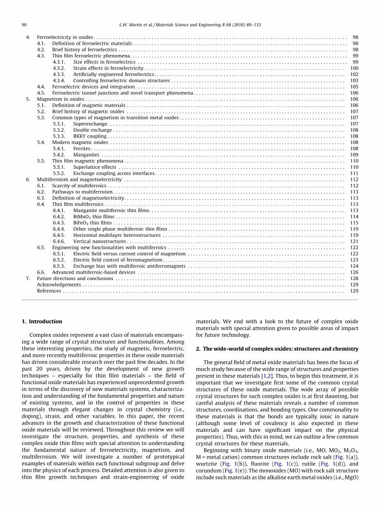
Beginning with binary oxide materials (i.e., MO, MO2, M2O3,M = metal cation) common structures include rock salt (Fig. 1(a)),wurtzite (Fig. 1(b)), fluorite (Fig. 1(c)), rutile (Fig. 1(d)), andcorundum (Fig. 1(e)). The monoxides (MO) with rock salt structureinclude such materials as the alkaline earth metal oxides (i.e., MgO)
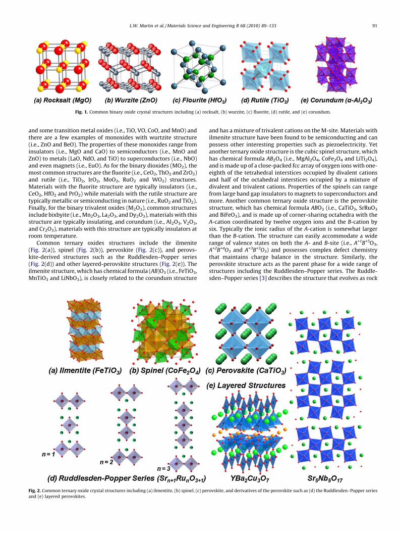
Fig. 1. Common binary oxide crystal structures including (a) rocksalt, (b) wurzite, (c) fluorite, (d) rutile, and (e) corundum.
L.W. Martin et al. / Materials Science and Engineering R 68 (2010) 89–133 91
and some transition metal oxides (i.e., TiO, VO, CoO, and MnO) andthere are a few examples of monoxides with wurtzite structure(i.e., ZnO and BeO). The properties of these monoxides range frominsulators (i.e., MgO and CaO) to semiconductors (i.e., MnO andZnO) to metals (LaO, NdO, and TiO) to superconductors (i.e., NbO)and even magnets (i.e., EuO). As for the binary dioxides (MO2), themost common structures are the fluorite (i.e., CeO2, ThO2 and ZrO2)and rutile (i.e., TiO2, IrO2, MoO2, RuO2 and WO2) structures.Materials with the fluorite structure are typically insulators (i.e.,CeO2, HfO2 and PrO2) while materials with the rutile structure aretypically metallic or semiconducting in nature (i.e., RuO2 and TiO2).Finally, for the binary trivalent oxides (M2O3), common structuresinclude bixbyite (i.e., Mn2O3, La2O3, and Dy2O3), materials with thisstructure are typically insulating, and corundum (i.e., Al2O3, V2O3,and Cr2O3), materials with this structure are typically insulators atroom temperature.
Common ternary oxides structures include the ilmenite(Fig. 2(a)), spinel (Fig. 2(b)), pervoskite (Fig. 2(c)), and perovs-kite-derived structures such as the Ruddlesden–Popper series(Fig. 2(d)) and other layered-perovskite structures (Fig. 2(e)). Theilmenite structure, which has chemical formula (AB)O3 (i.e., FeTiO3,MnTiO3 and LiNbO3), is closely related to the corundum structure
Fig. 2. Common ternary oxide crystal structures including (a) ilmentite, (b) spinel, (c) per
and (e) layered perovskites.
and has a mixture of trivalent cations on the M-site. Materials withilmenite structure have been found to be semiconducting and canpossess other interesting properties such as piezoelectricity. Yetanother ternary oxide structure is the cubic spinel structure, whichhas chemical formula AB2O4 (i.e., MgAl2O4, CoFe2O4 and LiTi2O4),and is made up of a close-packed fcc array of oxygen ions with one-eighth of the tetrahedral interstices occupied by divalent cationsand half of the octahedral interstices occupied by a mixture ofdivalent and trivalent cations. Properties of the spinels can rangefrom large band gap insulators to magnets to superconductors andmore. Another common ternary oxide structure is the perovskitestructure, which has chemical formula ABO3 (i.e., CaTiO3, SrRuO3
and BiFeO3), and is made up of corner-sharing octahedra with theA-cation coordinated by twelve oxygen ions and the B-cation bysix. Typically the ionic radius of the A-cation is somewhat largerthan the B-cation. The structure can easily accommodate a widerange of valence states on both the A- and B-site (i.e., A+1B+5O3,A+2B+4O3 and A+3B+3O3) and possesses complex defect chemistrythat maintains charge balance in the structure. Similarly, theperovskite structure acts as the parent phase for a wide range ofstructures including the Ruddlesden–Popper series. The Ruddle-sden–Popper series [3] describes the structure that evolves as rock
ovskite, and derivatives of the perovskite such as (d) the Ruddlesden–Popper series
L.W. Martin et al. / Materials Science and Engineering R 68 (2010) 89–13392
salt layers are inserted in the perovskite structure separating(0 0 1) planes and is written as An+1BnO3n+1 (where n =1 is theparent perovskite structure). The example shown here is for theRuddlesden–Popper series based on the widely studied metallic,ferromagnet SrRuO3. As rock salt layers are added to this structurethe properties can change quite drastically; the n = 1 phase(Sr2RuO4) is known to be a superconductor [4] while the n = 2phase (Sr3Ru2O7) exhibits complex magnetic structure andinteresting changes in resistance at low temperatures [5,6]. Othermore complicated layered structures can be derived from theperovskite structure such as those shown in Fig. 2(e) for the high-temperature superconductor YBa2Cu3O7. Key to the superconduct-ing properties observed in this material are the square-planarcoordinated CuO4 planes.
At the heart of understanding oxide materials, is recognizinghow the chemical structure of the material enables theevolution of the electronic structure. From chemical bondingto chemical doping, the interplay of physics and chemistry inoxide materials is a very rich subject. In the monoxides (MO)like the rock salt materials discussed above both the cation andthe O-anion are in octahedral coordination and they possesslargely ionic bonds and, therefore, typically have very large bandgaps and insulating properties. Monoxides with the wurtzitestructure, however, are hexagonal and possess tetrahedralcoordination of the cations and anions (very similar to adiamond cubic structure of many traditional semiconductorslike Si) and thus typically are more semiconducting in nature.This idea can be extended to a wide range of oxide materials, butis very elegantly described in the richness of properties found inthe perovskite-derived oxides.
By far the most interesting aspect of complex oxides, as isexemplified by the perovskites, is the ability to engineer/tune theirphysical properties simply by replacing the cationic species thatare located at the A-and B-sites in and around the oxygenoctahedral coordination cage. Thus, the electronic structure andcoordination chemistry of the cationic species controls thefundamental physical phenomena. As an example, let us take alook at the prototypical perovskite SrTiO3 which is a good insulatoras a consequence of the closed shell electronic structure of both Srand Ti (4+ and d0): from a band perspective, the valence band isfilled while the conduction band is empty. Simply changing the A-site cation from Sr to La makes a dramatic difference in theelectronic structure as well as the transport properties. In LaTiO3,the Ti in this compound is in the +3 oxidation state and thus in aformal sense has d1 electronic structure. As such, it is expected tobe a good conductor as a consequence; however, the reality issomething dramatically different. LaTiO3 is actually a very goodinsulator; a so-called Mott insulator [7]. This insulating behaviorarises due to the interplay between the kinetic energy of theelectron and Coulombic repulsion effects at the atomic scale. Thesetwo terms trade off of each other and so the manifested transportproperties are the result of this competition. Such materials exhibitstrong (sometimes colossal) changes in their transport propertiesunder external thermodynamic stimuli (i.e., temperature, mag-netic field, electric field and chemical potential). If one were to takethe LaTiO3 structure and change the cation at the B-site (thetransition metal site), for instance by replacing the Ti with Mn,then one will obtain the antiferromagnetic insulator (insulating forthe same reason as for LaTiO3) LaMnO3. There are a number ofexquisite treatise on the nature of electronic conduction in oxides(see, for example, Refs. [7,8]) and so we will not elaborate furtheron this subject here, except to note that the entire evolution of thephysics and chemistry of these materials and their implementationinto next-generation technologies is dependent on the complexinterplay between the cationic stereochemistry, electronic struc-ture and the interactions among them.
3. Advances in the growth of oxide thin films
The modern study of complex oxide materials has been drivenlargely by the development of new growth and characterizationtechniques that have offered researchers unprecedented access tonew phases and insight about these materials. The development ofnew thin film growth techniques that allow for the production ofnon-equilibrium phases of materials and strain engineering ofexisting materials represents a significant step forward in thestudy of functional complex oxide materials [9]. Epitaxial growthof thin films offers a pathway to the discovery and stabilization of anumber of new multiferroics in conjunction with the availability ofhigh quality materials that can be produced with larger lateralsizes than traditionally possible with single crystal samples.Ferroelectric, magnetic, and multiferroic thin films and nanos-tructures have been produced using a wide variety of growthtechniques including sputtering, spin coating, pulsed laserdeposition, sol–gel processes, metal-organic chemical vapordeposition, molecular beam epitaxy, and more. In this sectionwe will discuss the details of the growth of oxide thin films as wellas recent and future advances in in situ characterization andcontrol of the growth of oxide materials. We direct the reader toany of a number of excellent texts on the greater field of thin filmsgrowth and characterization for additional information (see, forinstance, Refs. [10,11]).
3.1. Thin film growth modes and epitaxy
We begin with a brief overview of thin film growth processes inmaterials. There are three major thin film growth modes: (1)Volmer–Weber or island growth, (2) Frank–Van der Merwe orlayer-by-layer growth, and (3) Stranski–Krastanov growth. Thesegrowth mechanisms are illustrated in Fig. 3. Volmer–Weber ofisland growth (Fig. 3(a)) occurs when the smallest stable clustersnucleate on the substrate and grow into three-dimensional islandfeatures. One simplistic explanation for this growth behavior isthat the atoms or molecules being deposited are more stronglybonded to each other than to the substrate material. This is oftenthe case when the film and substrate are dissimilar materials.There are a few example of such behavior in the growth of oxidefilms on oxide substrates, but this growth mode is typicallyobserved when metal and semiconductor (i.e., Group IV, III–V, etc.)films are grown on oxide substrates. The opposite characteristics,however, are displayed in Frank–Van der Merwe or layer-by-layergrowth (Fig. 3(b)) which occurs when the extension of the smallestnucleus occurs in two dimensions resulting in the formation ofplanar sheets. In layer-by-layer growth the depositing atoms ormolecules are more strongly bonded to the substrate than eachother and each layer is progressively less strongly bonded than theprevious layer. This effect extends continuously until the bulkbonding strength is reach. A typical example of this is the epitaxialgrowth of semiconductors and oxide materials. The greater field ofoxide thin film growth has developed around the ability to controlmaterials through this and other similar growth modes. Suchcapabilities have ushered in an era of unprecedented control ofoxide materials down to the single (or even half-) unit cell level.The final growth mechanism is the Stranski–Krastanov mode(Fig. 3(c)) which is a combination of the layer-by-layer and islandgrowth. In this growth mode, after forming one or moremonolayers in a layer-by-layer fashion, continued layer-by-layergrowth becomes energetically unfavorable and islands begin toform. This sort of growth is fairly common and has been observedin a number of metal–metal and metal–semiconductor systems[10].
These different growth modes can be described in more detailwith simple thermodynamic models for the nucleation and growth
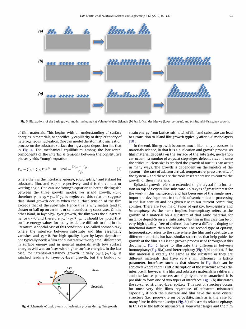
Fig. 3. Illustrations of the basic growth modes including (a) Volmer–Weber (island), (b) Frank–Van der Merwe (layer-by-layer), and (c) Stranski–Krastanov growth.
L.W. Martin et al. / Materials Science and Engineering R 68 (2010) 89–133 93
of film materials. This begins with an understanding of surfaceenergies in materials, or specifically capillarity or droplet theory ofheterogeneous nucleation. One can model the atomistic nucleationprocess on the substrate surface during a vapor deposition like thatin Fig. 4. The mechanical equilibrium among the horizontalcomponents of the interfacial tensions between the constitutivephases yields Young’s equation:
gsv ¼ g fs þ g f v cos u or cos u ¼ðgsv ¼ g fsÞ
g f v(1)
where the g is the interfacial energy, subscripts s, f, and v stand forsubstrate, film, and vapor respectively, and u is the contact orwetting angle. One can use Young’s equation to better distinguishbetween the three growth modes. For island growth, u > 0therefore gsv < gfs + gfv. If gfs is neglected, this relation suggeststhat island growth occurs when the surface tension of the filmexceeds that of the substrate. Hence this is why metals tend tocluster or ball up on ceramic or semiconducting substrates. On theother hand, in layer-by-layer growth, the film wets the substrate,hence u � 0 and therefore gsv � gfs + gfv. It should be noted thatsurface energy values for many oxide are difficult to find in theliterature. A special case of this condition is so-called homoepitaxywhere the interface between substrate and film essentiallyvanishes and gfs = 0. For high quality layer-by-layer depositionone typically needs a film and substrate with only small differencesin surface energy and in general materials with low surfaceenergies will wet surfaces with higher surface energies. In the lastcase, for Stranski–Krastanov growth initially gsv � gfs + gfv issatisfied leading to layer-by-layer growth, but the buildup of
Fig. 4. Schematic of basic atomistic nucleation process during film growth.
strain energy from lattice mismatch of film and substrate can leadto a transition to island like growth typically after 5–6 monolayers[10].
In the end, film growth becomes much like many processes inmaterials science, in that it is a nucleation and growth process. Asfilm material deposits on the surface of the substrate, nucleationcan occur in a number of ways, at step edges, defects, etc., and oncethe critical nucleus size is reached the growth of nucleus can occurin many ways. The growth is dependent on the kinetics of thesystem – the rate of adatom arrival, temperature, pressure, etc., ofthe system – and these are the tools researchers use to control thegrowth of their materials.
Epitaxial growth refers to extended single-crystal film forma-tion on top of a crystalline substrate. Epitaxy is of great interest forthe work in this manuscript and has been one of the single mostimportant developments in the field of semiconductor processingin the last century and has given rise to our current computingabilities. There are two major types of epitaxy, homoepitaxy andheteroepitaxy. As the name implies, homoepitaxy refers to thegrowth of a material on a substrate of that same material, forinstance doped-Si on a Si substrate. The film in this case can be ofvery high quality, free of defects, but have a different doping orfunctional nature then the substrate. The second type of epitaxy,heteroepitaxy, refers to the case where the film and substrate aredifferent materials, but have similar structures that help guide thegrowth of the film. This is the growth process used throughout thisdocument. Fig. 5 helps to illustrate the differences betweenhomoepitaxy (Fig. 5(a)) and heteroepitaxy (Fig. 5(b) and (c)). If thefilm material is exactly the same as the substrate or they aredifferent materials that have very small difference in latticeparameter, interfaces such as that shown in Fig. 5(a) can beachieved where there is little disruption of the structure across theinterface. If, however, the film and substrate materials are differentand the lattice parameters are slightly more mismatched, it ispossible to form one of two types of interfaces. Fig. 5(b) illustratesthe so-called strained-layer epitaxy. This sort of structure occursfor most very thin films regardless of substrate mismatchespecially if both the substrate and film have the same crystalstructure (i.e., perovskite on perovskite, such as is the case formany films in this manuscript). Fig. 5(c) illustrates relaxed epitaxy.In this case the lattice mismatch is somewhat larger and the film
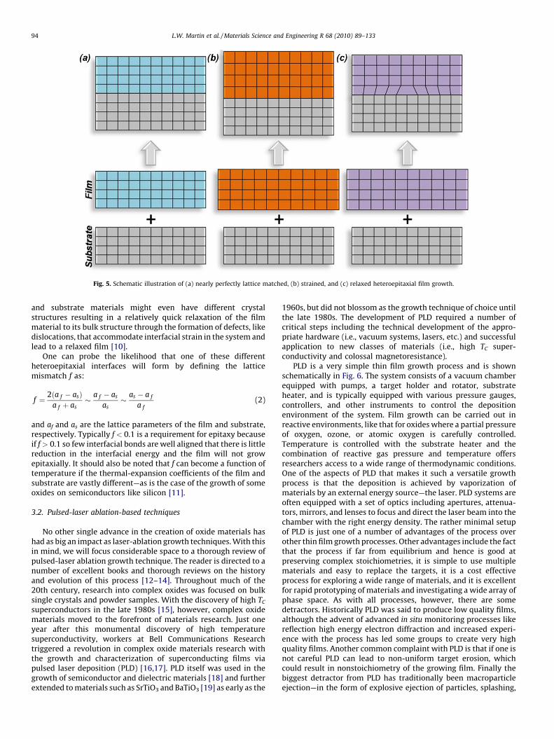
Fig. 5. Schematic illustration of (a) nearly perfectly lattice matched, (b) strained, and (c) relaxed heteroepitaxial film growth.
L.W. Martin et al. / Materials Science and Engineering R 68 (2010) 89–13394
and substrate materials might even have different crystalstructures resulting in a relatively quick relaxation of the filmmaterial to its bulk structure through the formation of defects, likedislocations, that accommodate interfacial strain in the system andlead to a relaxed film [10].
One can probe the likelihood that one of these differentheteroepitaxial interfaces will form by defining the latticemismatch f as:
f ¼2ða f � asÞ
a f þ as�
a f � as
as�
as � a f
a f(2)
and af and as are the lattice parameters of the film and substrate,respectively. Typically f < 0.1 is a requirement for epitaxy becauseif f > 0.1 so few interfacial bonds are well aligned that there is littlereduction in the interfacial energy and the film will not growepitaxially. It should also be noted that f can become a function oftemperature if the thermal-expansion coefficients of the film andsubstrate are vastly different—as is the case of the growth of someoxides on semiconductors like silicon [11].
3.2. Pulsed-laser ablation-based techniques
No other single advance in the creation of oxide materials hashad as big an impact as laser-ablation growth techniques. With thisin mind, we will focus considerable space to a thorough review ofpulsed-laser ablation growth technique. The reader is directed to anumber of excellent books and thorough reviews on the historyand evolution of this process [12–14]. Throughout much of the20th century, research into complex oxides was focused on bulksingle crystals and powder samples. With the discovery of high TC
superconductors in the late 1980s [15], however, complex oxidematerials moved to the forefront of materials research. Just oneyear after this monumental discovery of high temperaturesuperconductivity, workers at Bell Communications Researchtriggered a revolution in complex oxide materials research withthe growth and characterization of superconducting films viapulsed laser deposition (PLD) [16,17]. PLD itself was used in thegrowth of semiconductor and dielectric materials [18] and furtherextended to materials such as SrTiO3 and BaTiO3 [19] as early as the
1960s, but did not blossom as the growth technique of choice untilthe late 1980s. The development of PLD required a number ofcritical steps including the technical development of the appro-priate hardware (i.e., vacuum systems, lasers, etc.) and successfulapplication to new classes of materials (i.e., high TC super-conductivity and colossal magnetoresistance).
PLD is a very simple thin film growth process and is shownschematically in Fig. 6. The system consists of a vacuum chamberequipped with pumps, a target holder and rotator, substrateheater, and is typically equipped with various pressure gauges,controllers, and other instruments to control the depositionenvironment of the system. Film growth can be carried out inreactive environments, like that for oxides where a partial pressureof oxygen, ozone, or atomic oxygen is carefully controlled.Temperature is controlled with the substrate heater and thecombination of reactive gas pressure and temperature offersresearchers access to a wide range of thermodynamic conditions.One of the aspects of PLD that makes it such a versatile growthprocess is that the deposition is achieved by vaporization ofmaterials by an external energy source—the laser. PLD systems areoften equipped with a set of optics including apertures, attenua-tors, mirrors, and lenses to focus and direct the laser beam into thechamber with the right energy density. The rather minimal setupof PLD is just one of a number of advantages of the process overother thin film growth processes. Other advantages include the factthat the process if far from equilibrium and hence is good atpreserving complex stoichiometries, it is simple to use multiplematerials and easy to replace the targets, it is a cost effectiveprocess for exploring a wide range of materials, and it is excellentfor rapid prototyping of materials and investigating a wide array ofphase space. As with all processes, however, there are somedetractors. Historically PLD was said to produce low quality films,although the advent of advanced in situ monitoring processes likereflection high energy electron diffraction and increased experi-ence with the process has led some groups to create very highquality films. Another common complaint with PLD is that if one isnot careful PLD can lead to non-uniform target erosion, whichcould result in nonstoichiometry of the growing film. Finally thebiggest detractor from PLD has traditionally been macroparticleejection—in the form of explosive ejection of particles, splashing,
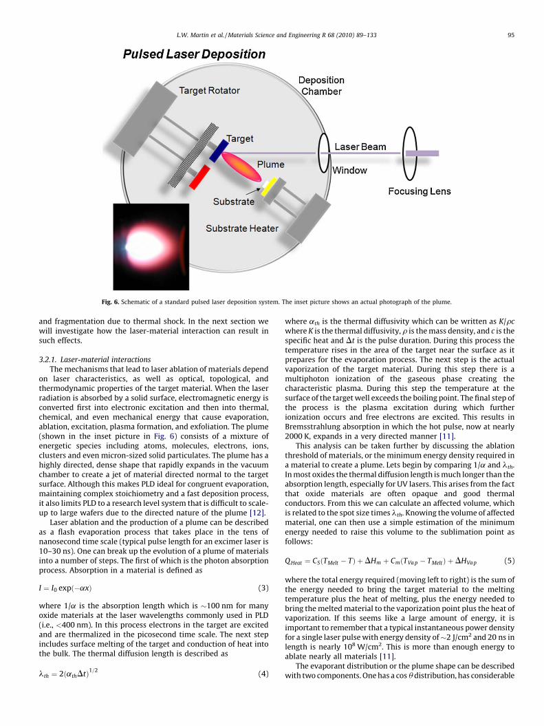
Fig. 6. Schematic of a standard pulsed laser deposition system. The inset picture shows an actual photograph of the plume.
L.W. Martin et al. / Materials Science and Engineering R 68 (2010) 89–133 95
and fragmentation due to thermal shock. In the next section wewill investigate how the laser-material interaction can result insuch effects.
3.2.1. Laser-material interactions
The mechanisms that lead to laser ablation of materials dependon laser characteristics, as well as optical, topological, andthermodynamic properties of the target material. When the laserradiation is absorbed by a solid surface, electromagnetic energy isconverted first into electronic excitation and then into thermal,chemical, and even mechanical energy that cause evaporation,ablation, excitation, plasma formation, and exfoliation. The plume(shown in the inset picture in Fig. 6) consists of a mixture ofenergetic species including atoms, molecules, electrons, ions,clusters and even micron-sized solid particulates. The plume has ahighly directed, dense shape that rapidly expands in the vacuumchamber to create a jet of material directed normal to the targetsurface. Although this makes PLD ideal for congruent evaporation,maintaining complex stoichiometry and a fast deposition process,it also limits PLD to a research level system that is difficult to scale-up to large wafers due to the directed nature of the plume [12].
Laser ablation and the production of a plume can be describedas a flash evaporation process that takes place in the tens ofnanosecond time scale (typical pulse length for an excimer laser is10–30 ns). One can break up the evolution of a plume of materialsinto a number of steps. The first of which is the photon absorptionprocess. Absorption in a material is defined as
I ¼ I0 expð�axÞ (3)
where 1/a is the absorption length which is �100 nm for manyoxide materials at the laser wavelengths commonly used in PLD(i.e., <400 nm). In this process electrons in the target are excitedand are thermalized in the picosecond time scale. The next stepincludes surface melting of the target and conduction of heat intothe bulk. The thermal diffusion length is described as
lth ¼ 2ðathDtÞ1=2(4)
where ath is the thermal diffusivity which can be written as K/rc
where K is the thermal diffusivity, r is the mass density, and c is thespecific heat and Dt is the pulse duration. During this process thetemperature rises in the area of the target near the surface as itprepares for the evaporation process. The next step is the actualvaporization of the target material. During this step there is amultiphoton ionization of the gaseous phase creating thecharacteristic plasma. During this step the temperature at thesurface of the target well exceeds the boiling point. The final step ofthe process is the plasma excitation during which furtherionization occurs and free electrons are excited. This results inBremsstrahlung absorption in which the hot pulse, now at nearly2000 K, expands in a very directed manner [11].
This analysis can be taken further by discussing the ablationthreshold of materials, or the minimum energy density required ina material to create a plume. Lets begin by comparing 1/a and lth.In most oxides the thermal diffusion length is much longer than theabsorption length, especially for UV lasers. This arises from the factthat oxide materials are often opaque and good thermalconductors. From this we can calculate an affected volume, whichis related to the spot size times lth. Knowing the volume of affectedmaterial, one can then use a simple estimation of the minimumenergy needed to raise this volume to the sublimation point asfollows:
QHeat ¼ CSðTMelt � TÞ þDHm þ CmðTVa p � TMeltÞ þDHVa p (5)
where the total energy required (moving left to right) is the sum ofthe energy needed to bring the target material to the meltingtemperature plus the heat of melting, plus the energy needed tobring the melted material to the vaporization point plus the heat ofvaporization. If this seems like a large amount of energy, it isimportant to remember that a typical instantaneous power densityfor a single laser pulse with energy density of�2 J/cm2 and 20 ns inlength is nearly 108 W/cm2. This is more than enough energy toablate nearly all materials [11].
The evaporant distribution or the plume shape can be describedwith two components. One has a cos u distribution, has considerable
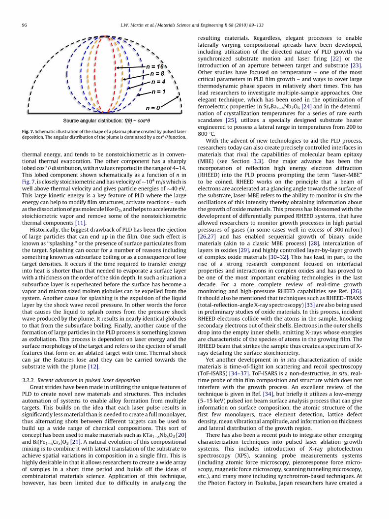
Fig. 7. Schematic illustration of the shape of a plasma plume created by pulsed laser
deposition. The angular distribution of the plume is dominated by a cosn u function.
L.W. Martin et al. / Materials Science and Engineering R 68 (2010) 89–13396
thermal energy, and tends to be nonstoichiometric as in conven-tional thermal evaporation. The other component has a sharplylobed cosn udistribution, with n values reported in the range of 4–14.This lobed component shown schematically as a function of n inFig. 7, is closely stoichiometric and has velocity of�104 m/s which iswell above thermal velocity and gives particle energies of �40 eV.This large kinetic energy is a key feature of PLD where the largeenergy can help to modify film structures, activate reactions – suchas the dissociation of gas molecule like O2, and helps to accelerate thestoichiometric vapor and remove some of the nonstoichiometricthermal components [11].
Historically, the biggest drawback of PLD has been the ejectionof large particles that can end up in the film. One such effect isknown as ‘‘splashing,’’ or the presence of surface particulates fromthe target. Splashing can occur for a number of reasons includingsomething known as subsurface boiling or as a consequence of lowtarget densities. It occurs if the time required to transfer energyinto heat is shorter than that needed to evaporate a surface layerwith a thickness on the order of the skin depth. In such a situation asubsurface layer is superheated before the surface has become avapor and micron sized molten globules can be expelled from thesystem. Another cause for splashing is the expulsion of the liquidlayer by the shock wave recoil pressure. In other words the forcethat causes the liquid to splash comes from the pressure shockwave produced by the plume. It results in nearly identical globulesto that from the subsurface boiling. Finally, another cause of theformation of large particles in the PLD process is something knownas exfoliation. This process is dependent on laser energy and thesurface morphology of the target and refers to the ejection of smallfeatures that form on an ablated target with time. Thermal shockcan jar the features lose and they can be carried towards thesubstrate with the plume [12].
3.2.2. Recent advances in pulsed laser deposition
Great strides have been made in utilizing the unique features ofPLD to create novel new materials and structures. This includesautomation of systems to enable alloy formation from multipletargets. This builds on the idea that each laser pulse results insignificantly less material than is needed to create a full monolayer,thus alternating shots between different targets can be used tobuild up a wide range of chemical compositions. This sort ofconcept has been used to make materials such as KTa1�xNbxO3 [20]and Bi(Fe1�xCrx)O3 [21]. A natural evolution of this compositionalmixing is to combine it with lateral translation of the substrate toachieve spatial variations in composition in a single film. This ishighly desirable in that it allows researchers to create a wide arrayof samples in a short time period and builds off the ideas ofcombinatorial materials science. Application of this technique,however, has been limited due to difficulty in analyzing the
resulting materials. Regardless, elegant processes to enablelaterally varying compositional spreads have been developed,including utilization of the directed nature of PLD growth viasynchronized substrate motion and laser firing [22] or theintroduction of an aperture between target and substrate [23].Other studies have focused on temperature – one of the mostcritical parameters in PLD film growth – and ways to cover largethermodynamic phase spaces in relatively short times. This haslead researchers to investigate multiple-sample approaches. Oneelegant technique, which has been used in the optimization offerroelectric properties in SrxBa1�xNb2O6 [24] and in the determi-nation of crystallization temperatures for a series of rare earthscandates [25], utilizes a specially designed substrate heaterengineered to possess a lateral range in temperatures from 200 to800 8C.
With the advent of new technologies to aid the PLD process,researchers today can also create precisely controlled interfaces inmaterials that rival the capabilities of molecular beam epitaxy(MBE) (see Section 3.3). One major advance has been theincorporation of reflection high energy electron diffraction(RHEED) into the PLD process prompting the term ‘‘laser-MBE’’to be coined. RHEED works on the principle that a beam ofelectrons are accelerated at a glancing angle towards the surface ofthe substrate, laser-MBE refers to the ability to monitor in situ theoscillations of this intensity thereby obtaining information aboutthe growth of oxide materials. This process has blossomed with thedevelopment of differentially pumped RHEED systems, that haveallowed researchers to monitor growth processes in high partialpressures of gases (in some cases well in excess of 300 mTorr)[26,27] and has enabled sequential growth of binary oxidematerials (akin to a classic MBE process) [28], intercalation oflayers in oxides [29], and highly controlled layer-by-layer growthof complex oxide materials [30–32]. This has lead, in part, to therise of a strong research component focused on interfacialproperties and interactions in complex oxides and has proved tobe one of the most important enabling technologies in the lastdecade. For a more complete review of real-time growthmonitoring and high-pressure RHEED capabilities see Ref. [26].It should also be mentioned that techniques such as RHEED-TRAXS(total-reflection-angle X-ray spectroscopy) [33] are also being usedin preliminary studies of oxide materials. In this process, incidentRHEED electrons collide with the atoms in the sample, knockingsecondary electrons out of their shells. Electrons in the outer shellsdrop into the empty inner shells, emitting X-rays whose energiesare characteristic of the species of atoms in the growing film. TheRHEED beam that strikes the sample thus creates a spectrum of X-rays detailing the surface stoichiometry.
Yet another development in in situ characterization of oxidematerials is time-of-flight ion scattering and recoil spectroscopy(ToF-ISARS) [34–37]. ToF-ISARS is a non-destructive, in situ, real-time probe of thin film composition and structure which does notinterfere with the growth process. An excellent review of thetechnique is given in Ref. [34], but briefly it utilizes a low-energy(5–15 keV) pulsed ion beam surface analysis process that can giveinformation on surface composition, the atomic structure of thefirst few monolayers, trace element detection, lattice defectdensity, mean vibrational amplitude, and information on thicknessand lateral distribution of the growth region.
There has also been a recent push to integrate other emergingcharacterization techniques into pulsed laser ablation growthsystems. This includes introduction of X-ray photoelectronspectroscopy (XPS), scanning probe measurements systems(including atomic force microscopy, piezoresponse force micro-scopy, magnetic force microscopy, scanning tunneling microscopy,etc.), and many more including synchrotron-based techniques. Atthe Photon Factory in Tsukuba, Japan researchers have created a
L.W. Martin et al. / Materials Science and Engineering R 68 (2010) 89–133 97
high-resolution synchrotron-radiation angle-resolved photoemis-sion spectrometer (ARPES) combined with a combinatorial laser-MBE growth system to investigate the electronic structure oftransition metal oxide thin films [38]. Around this same time, time-resolved X-ray diffraction studies of the PLD process werecompleted at the UNICAT undulator beamline at the AdvancedPhoton Source located at Argonne National Laboratory [39]. Asimilar system has since been constructed at the EuropeanSynchrotron Radiation Facility in Grenoble, France [40]. At theCornell High Energy Synchrotron Source (CHESS), researchers havedeveloped a laser-ablation growth system equipped with in situ X-ray reflectivity capabilities that enable careful studies of thin filmgrowth morphology [41].
3.3. Molecular beam epitaxy
Long the standard of comparison for high-precision growth,molecular beam epitaxy (MBE), has a strong history in the growthof complex oxide materials, beginning with work in the late 1980sin pursuit of better high-TC superconductor phases [42,43]. Withinyears, again driven by the search for higher and higher TC incomplex oxide superconductors, numerous reports on the growthof superconducting materials using molecular beam epitaxy drovenew innovations—including growth in ozone [44]. A number ofrecent reviews cover the developments and use of MBE in thegrowth of oxide materials in some detail (see, for instance, Refs.[45–47]). In contrast to PLD, MBE involves the generation of lowenergy (�1 eV) thermal atomic beams for each of the constituentmaterials desired in the film (both cations such as transition metalsand anions such as oxygen). Beams of metal atoms can be createdusing either radiatively heated sources (i.e., Knudsen or effusioncells) or from electron beam evaporators. Oxygen is typicallysupplied either as molecular oxygen (O2), ozone (O3), or atomicoxygen (O)—due to greatly enhanced oxidizing potentials ozoneand atomic oxygen are commonly used today to assure growth of afully oxidized film. The high purity of commercially available metaland O2 materials means that MBE techniques can be used toproduce extremely pure and defect-free films of complex oxides[47]. Although the quality of materials created by MBE is very good,widespread usage of this technique is limited due to a number offactors including high system, component, and materials prices (agood MBE system can cost well in excess of $1 million), therequirement of UHV background pressures, and limited materialsflexibility compared to other growth processes. Regardless, MBEand MBE-like systems (i.e., systems possessing near UHV back-ground vacuum levels, and load-lock assemblies) stand to makeserious impact in next generation materials science. By combiningcutting-edge thin film growth techniques together with a wide-range of materials characterization methods, major stumblingblocks in the pursuit of science will be overcome.
3.4. Sputtering
The basic sputtering process has been known and used for manyyears since the development of ‘‘conventional’’ magnetrons in theearly 1970s, was greatly improved with the development ofunbalanced magnetrons in the 1980s, and with the incorporationof multi-source ‘‘closed-field’’ systems in the 1990s [48]. The termsputtering, typically refers to the process known as magnetronsputtering where a target (or cathode) plate is bombarded byenergetic ions generated in a glow discharge plasma situated infront of the target. This is a classic physical deposition processwhereby the bombardment process ejects atoms from the target asa result of a collision cascade that subsequently deposit the film[49]. For a detailed description of recent advances in sputteringtechnology, the reader is directed to the review by Kelly and Arnell
[48]. For the sake of space, here we will focus on sputter growth ofoxide thin films. Over the years, a wide range of oxide materials hasbeen grown via sputter deposition processes. Although pulsedlaser ablation techniques are good a maintaining complexstoichiometries in oxides, such processes are not scalable.Sputtering, on the other hand, is a widely used depositiontechnique for large-scale production. With the advent of multi-source deposition, significant advances in sputtering of complexchemical composition materials have been obtained. Thus,sputtering has been used to make semiconductor, dielectric,insulating, magnetic, and superconducting oxide materials as wellas catalysts, protective coatings, and more [50]. Key to the ability tocreate high quality oxide thin films is intimate knowledge ofsputtering yields of the various chemical species in a material (asdifferent elements are sputtered at different rates from targets,starting composition may need to be carefully tuned to givestoichiometric final films), deposition rate is key for controlling thecrystal phase, temperatures for microstructure, sputtering atmo-sphere is important in controlling surface structure, and substrateposition or bias voltage is key in determining the types and densityof defects in these films. Several sputter deposition techniqueshave been used in the growth of oxide thin films including on-axisdc magnetron sputtering [51], cylindrical magnetron sputtering[52], ion-beam sputtering [53], and off-axis sputtering [54]. Ofparticular interest for the growth of oxide thin films is the use of areactive gas – such as pure O2 or Ar/O2 mixtures – which helpsassure oxygen stoichiometry is close to the desired level. For amore detailed discussion of the evolution of sputtering growth(especially in terms of work on ferroelectric materials) see thereview by Schwarzkopf and Fornari [55].
3.5. Metal-organic chemical vapor deposition
Metal-organic chemical vapor deposition (MOCVD) is of greatimportance for large-scale production of oxide thin films [56]. It isroutinely used in the electronics industry, has excellent filmuniformity over large areas, is capable of conformal coating ofarbitrary geometries, can be done at relatively high partialpressures of oxygen, has easy and reproducible control of filmstoichiometry, has relatively high deposition rates, and allows formultilayer growth, superlattices, and graded compositions [2,55].MOCVD works on the principle that one can create a complexorganic molecule decorated with the material desired for thin filmgrowth. By passing an inert gas through a bubbler of a liquidprecursor, these molecules are transported to the reactionchamber and passed over a substrate at high temperature. Theheat helps to break the molecules and deposits the desiredmaterial on the surface. One of the biggest challenges for MOCVDgrowth of oxide materials is identification of the appropriatemetal-organic precursors. Precursors for materials with highatomic number typically have limited vapor pressure at roomtemperature and thus it is essential to heat the bubblers and all thelines in the system to avoid clogging. This requires carefulattention so as to avoid hot spots where premature depositionmight occur as well as cool spots where condensation of theprecursor can occur. In the end, very high quality thin films of oxidematerials can be created using this technique. Again, for a morethorough review of the MOCVD process, precursors, and specificdetails in reference to ferroelectric materials please see Ref. [55].
3.6. Solution-based thin film deposition techniques
There are a variety of solution-based approaches for thecreation of complex oxide materials including sol–gel, chelate, andmetaloorganic decomposition (for good reviews, see Refs. [57,58]).Very briefly, solution deposition usually involves four steps: (1)
L.W. Martin et al. / Materials Science and Engineering R 68 (2010) 89–13398
synthesis of the precursor solution, (2) deposition by spin-castingor dip-coating, (3) low-temperature heat treatment for drying and/or pyrolosis of organics, and formation of amorphous films(typically 300–400 8C), (4) high temperature heat treatment fordensification and crystallization (anywhere from 600 to 1100 8C).Such processes are highly scalable, cheap, and very quick. Greatstrides have been made in utilizing such techniques to make highquality and highly oriented films for devices.
3.7. Low-temperature aqueous solution depositions
In stark contrast to the previously reported growth techniques,there is a set of aqueous solution-based deposition techniques thatenable the creation of films at lower temperatures (25–100 8C).Processes such as chemical bath deposition (CBD), successive ionlayer adsorption and reaction (SILAR), liquid phase deposition(LPD), electroless deposition (ED), as well as more modern variantssuch as photochemical deposition (PCD), deposition assisted byapplied fields, ferrite plating, liquid flow deposition, and more canbe used to create films of oxide materials at low temperatures. Fora detailed review see Ref. [59].
4. Ferroelectricity in oxides
4.1. Definition of ferroelectric materials
Of the 32 crystal classes of materials, 11 posses centers ofsymmetry and hence possess no polar properties. Of the remaining21, all but one exhibit electrical polarity when subjected to a stressand are called piezoelectric. Of the 20 piezoelectric crystal classes,10 show a unique polar axis. These crystals are called polar becausethey possess a spontaneous polarization [60]. Typically such aspontaneous polarization cannot be detected by the presence ofcharge on the surface of the crystal as free charge within the crystalflows to screen or compensate the polarization. One can, however,often detect the presence of a spontaneous polarization bystudying the temperature dependent changes in polarizationwhich results in the flow of charge to and from the surfaces. This isknown as the pyroelectric effect and these 10 polar crystal classesare often referred to as the pyroelectric classes. A material is said tobe ferroelectric when it has two or more orientational states in theabsence of an electric field and can be shifted from one to anotherof these states by an electric field. Any two of the orientationalstates are identical in crystal structure and differ only in electricpolarization at zero applied field [61]. Ferroelectric materials areinvariant under time reversal symmetry, but must break spatialinversion symmetry. Ferroelectrics are materials that undergo aphase transition from a high-temperature phase that behaves as anordinary dielectric to a low temperature phase that has aspontaneous polarization whose direction can be switched byan applied electric field. Any lattice of oppositely signed pointcharges is inherently unstable and relies on short-range interac-tions between adjacent electron clouds in the material to stabilizethe structure. In ferroelectric materials these interactions result inthe formation of a double-well potential that stabilizes a distortedstructure over the symmetric structure. In the case of classicperovskite ferroelectrics like PbTiO3 and BaTiO3 the Ti 3d – O 2p
orbital hybridization is essential for stabilizing the ferroelectricdistortion. It has also been found that most perovskite ferro-electrics have B-site ions that are formally d0 in nature and thus thelowest unoccupied energy levels are the d states and they tend tohybridized with the O 2p orbitals resulting in the double wellpotential [62]. A material is said to be a ferroelastic when it has twoor more orientation states in the absence of mechanical stress (andelectric field) and can be shifted from one to another of these statesby mechanical stress. It is imperative that two of the orientational
states are identical or enantiomorophous in crystal structure anddifferent in mechanical strain tensor at null mechanical stress (andelectric field) [61].
4.2. Brief history of ferroelectrics
The modern field of ferroelectrics finds its roots over 150 yearsago in studies of pyroelectric effects in materials completed duringthe mid-1850s [63]. By the late 1800s, the Curies had discoveredpiezoelectricity [64], but the idea of ferroelectricity remainedsomewhat elusive until the 1920s when researchers working onRochelle salt (NaKC4H4O6�4H2O) discovered that the polarizationof this material could be switched by an external electric field andquickly drew comparisons with ferromagnetic materials such asiron [65]. Despite early use of terms such as ‘‘Curie point,’’ the termferroelectricity did not come into wide spread use until the 1940s[66]. The late 1930s and 1940s, however, ushered in new life for thefield of ferroelectrics. Busch and Scherrer in Zurich produced thefirst series of ferroelectric crystals [67,68]. These crystals, based onthe phosphates (such as KH2PO4) and arsenates, proved thatferroelectricity was not a fluke discovery. Significant world eventsquickly forced these materials into service in devices – (NH4)H2PO4
became the principal underwater sound transducer and submarinedetector in World War II [61]. Around the same time, the firstmicroscopic model of ferroelectricity was developed by Slater andit has withstood the test of time quite well [69].
The modern field of oxide ferroelectrics was jumped started in1945 when BaTiO3 ceramics were found to possess dielectricconstants between 1000 and 3000 at room temperature [70]. Linesand Glass mark this event with some significance as it representedthe first ferroelectric without hydrogen bonds, the first with morethan one ferroelectric phase, the first with a non-piezoelectricprototype or paraelectric phase, and the most chemically simple ofall ferroelectrics discovered to date [61]. This material representedthe first of what has become the largest single class of ferro-electrics. By 1950, ferroelectricity had been discovered in KNbO3
and KTaO3 [71], LiNbO3 and LiTaO3 [72], and PbTiO3 [73]. From1945 to 1960, great strides were made in understanding thefundamental mechanisms for ferroelectricity. Starting from themacroscopic level, Ginzburg [74] and Devonshire [75] developedgroundbreaking work that assumed that the same energy functionis capable of describing both polar and non-polar phases and thiswas extended to antiferroelectrics soon after by Kittel [76]. On themicroscopic level, Slater developed the fundamental frameworkfor displacive transitions in 1950 and Anderson [77] and Cochran[78] developed the idea of a ‘‘rattling’’ ion within the framework oflattice dynamics, especially soft modes in materials. But the field ofoxide ferroelectrics really came into its own in the 1960s and1970s. With advances in theoretical pictures for the behavior, insynthesis of materials, and new characterization methods, ferro-electrics were thrust to the forefront of solid state physics research.It is this era that has built up much of the fundamentalunderstanding and knowledge that has enabled modern advancesin ferroelectric materials. For a wonderful jaunt through thehistory of ferroelectrics the reader is directed to the excellent bookby Lines and Glass [61] and a delightful perspective by Ginzburg[79].
What has been discovered, is that although most ferroelectricmaterials are not oxides, it is the oxide ferroelectrics that possessthe robust properties and great potential for practical applications.Ferroelectric perovskites, such as Pb(Zrx,Ti1�x)O3 (PZT), BaTiO3
(BTO), and BiFeO3 (BFO), have attracted a lot of attention withrespect to potential application in ultrahigh density memorydevices [80]. The magnitude and stability of the switchableferroelectric polarization are the central figures of merit for suchdevices. However, in general it is necessary to stabilize local
L.W. Martin et al. / Materials Science and Engineering R 68 (2010) 89–133 99
polarization with a critical polarized volume to break thesymmetry. Such an expectation results from the screening ofthe depolarization field, which becomes much stronger when thefilm thickness is reduced. This intriguing phenomenon plays a keyrole in the area of thin film and nanostructured ferroelectrics.
4.3. Thin film ferroelectric phenomena
Using thin film epitaxy it is possible to dramatically engineerand control ferroelectric materials. This includes the observation ofa number of intriguing phenomena including size effects, strainenhancement of and driven ferroelectricity, engineered ferroelec-tricity through superlattice growth, as well as deterministiccontrol of ferroelectric domain structures in materials. In thissection, we examine the developments of such work in thin filmferroelectrics.
4.3.1. Size effects in ferroelectrics
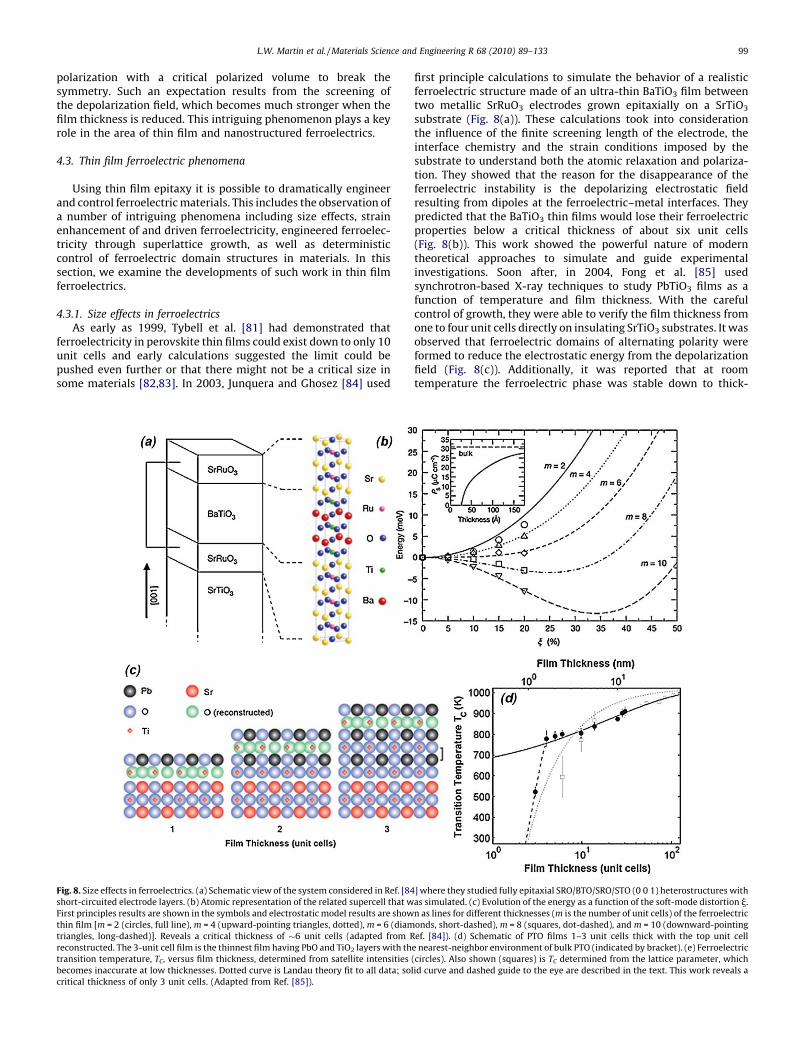
As early as 1999, Tybell et al. [81] had demonstrated thatferroelectricity in perovskite thin films could exist down to only 10unit cells and early calculations suggested the limit could bepushed even further or that there might not be a critical size insome materials [82,83]. In 2003, Junquera and Ghosez [84] used
Fig. 8. Size effects in ferroelectrics. (a) Schematic view of the system considered in Ref. [84
short-circuited electrode layers. (b) Atomic representation of the related supercell that w
First principles results are shown in the symbols and electrostatic model results are show
thin film [m = 2 (circles, full line), m = 4 (upward-pointing triangles, dotted), m = 6 (diam
triangles, long-dashed)]. Reveals a critical thickness of �6 unit cells (adapted from R
reconstructed. The 3-unit cell film is the thinnest film having PbO and TiO2 layers with th
transition temperature, TC, versus film thickness, determined from satellite intensities
becomes inaccurate at low thicknesses. Dotted curve is Landau theory fit to all data; sol
critical thickness of only 3 unit cells. (Adapted from Ref. [85]).
first principle calculations to simulate the behavior of a realisticferroelectric structure made of an ultra-thin BaTiO3 film betweentwo metallic SrRuO3 electrodes grown epitaxially on a SrTiO3
substrate (Fig. 8(a)). These calculations took into considerationthe influence of the finite screening length of the electrode, theinterface chemistry and the strain conditions imposed by thesubstrate to understand both the atomic relaxation and polariza-tion. They showed that the reason for the disappearance of theferroelectric instability is the depolarizing electrostatic fieldresulting from dipoles at the ferroelectric–metal interfaces. Theypredicted that the BaTiO3 thin films would lose their ferroelectricproperties below a critical thickness of about six unit cells(Fig. 8(b)). This work showed the powerful nature of moderntheoretical approaches to simulate and guide experimentalinvestigations. Soon after, in 2004, Fong et al. [85] usedsynchrotron-based X-ray techniques to study PbTiO3 films as afunction of temperature and film thickness. With the carefulcontrol of growth, they were able to verify the film thickness fromone to four unit cells directly on insulating SrTiO3 substrates. It wasobserved that ferroelectric domains of alternating polarity wereformed to reduce the electrostatic energy from the depolarizationfield (Fig. 8(c)). Additionally, it was reported that at roomtemperature the ferroelectric phase was stable down to thick-
] where they studied fully epitaxial SRO/BTO/SRO/STO (0 0 1) heterostructures with
as simulated. (c) Evolution of the energy as a function of the soft-mode distortion j.
n as lines for different thicknesses (m is the number of unit cells) of the ferroelectric
onds, short-dashed), m = 8 (squares, dot-dashed), and m = 10 (downward-pointing
ef. [84]). (d) Schematic of PTO films 1–3 unit cells thick with the top unit cell
e nearest-neighbor environment of bulk PTO (indicated by bracket). (e) Ferroelectric
(circles). Also shown (squares) is TC determined from the lattice parameter, which
id curve and dashed guide to the eye are described in the text. This work reveals a
L.W. Martin et al. / Materials Science and Engineering R 68 (2010) 89–133100
nesses of just 3 unit cells (Fig. 8(d)), which implies that, for allpractical matters, there is no size limit for the creation of aferroelectric material.
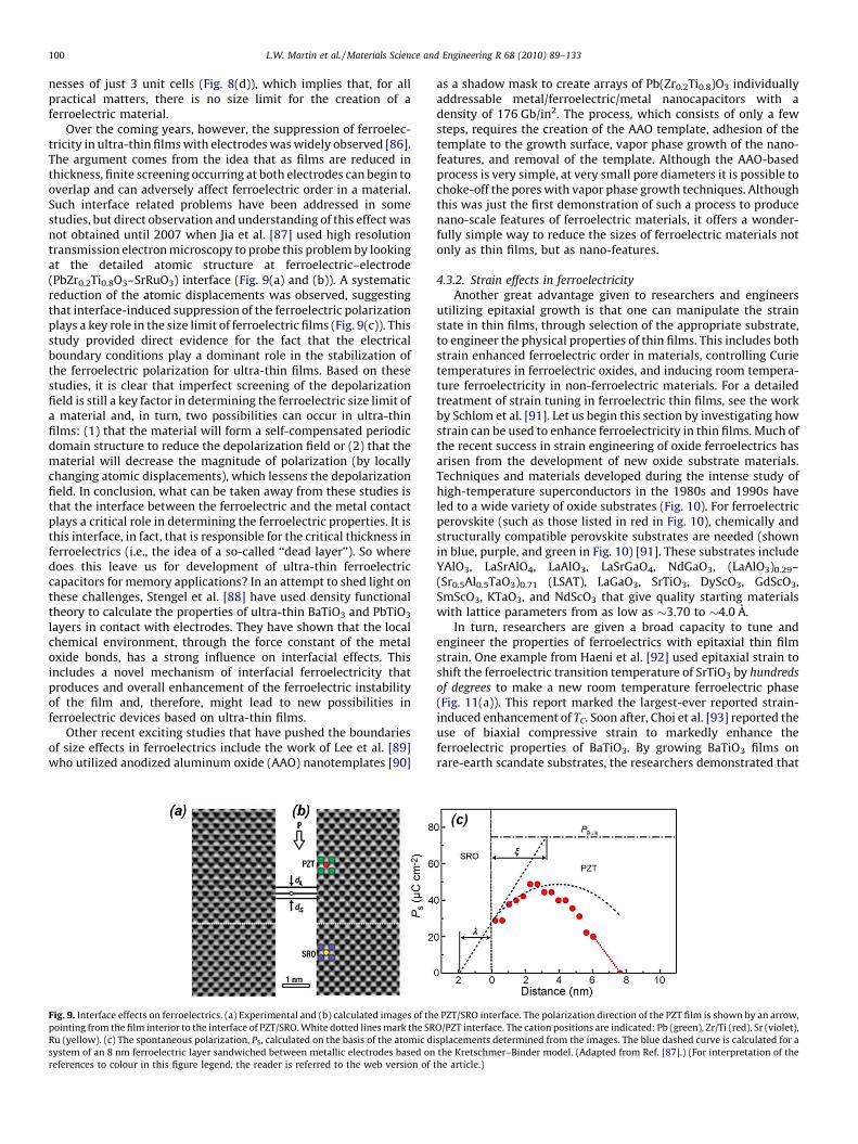
Over the coming years, however, the suppression of ferroelec-tricity in ultra-thin films with electrodes was widely observed [86].The argument comes from the idea that as films are reduced inthickness, finite screening occurring at both electrodes can begin tooverlap and can adversely affect ferroelectric order in a material.Such interface related problems have been addressed in somestudies, but direct observation and understanding of this effect wasnot obtained until 2007 when Jia et al. [87] used high resolutiontransmission electron microscopy to probe this problem by lookingat the detailed atomic structure at ferroelectric–electrode(PbZr0.2Ti0.8O3–SrRuO3) interface (Fig. 9(a) and (b)). A systematicreduction of the atomic displacements was observed, suggestingthat interface-induced suppression of the ferroelectric polarizationplays a key role in the size limit of ferroelectric films (Fig. 9(c)). Thisstudy provided direct evidence for the fact that the electricalboundary conditions play a dominant role in the stabilization ofthe ferroelectric polarization for ultra-thin films. Based on thesestudies, it is clear that imperfect screening of the depolarizationfield is still a key factor in determining the ferroelectric size limit ofa material and, in turn, two possibilities can occur in ultra-thinfilms: (1) that the material will form a self-compensated periodicdomain structure to reduce the depolarization field or (2) that thematerial will decrease the magnitude of polarization (by locallychanging atomic displacements), which lessens the depolarizationfield. In conclusion, what can be taken away from these studies isthat the interface between the ferroelectric and the metal contactplays a critical role in determining the ferroelectric properties. It isthis interface, in fact, that is responsible for the critical thickness inferroelectrics (i.e., the idea of a so-called ‘‘dead layer’’). So wheredoes this leave us for development of ultra-thin ferroelectriccapacitors for memory applications? In an attempt to shed light onthese challenges, Stengel et al. [88] have used density functionaltheory to calculate the properties of ultra-thin BaTiO3 and PbTiO3
layers in contact with electrodes. They have shown that the localchemical environment, through the force constant of the metaloxide bonds, has a strong influence on interfacial effects. Thisincludes a novel mechanism of interfacial ferroelectricity thatproduces and overall enhancement of the ferroelectric instabilityof the film and, therefore, might lead to new possibilities inferroelectric devices based on ultra-thin films.
Other recent exciting studies that have pushed the boundariesof size effects in ferroelectrics include the work of Lee et al. [89]who utilized anodized aluminum oxide (AAO) nanotemplates [90]
Fig. 9. Interface effects on ferroelectrics. (a) Experimental and (b) calculated images of th
pointing from the film interior to the interface of PZT/SRO. White dotted lines mark the SR
Ru (yellow). (c) The spontaneous polarization, PS, calculated on the basis of the atomic di
system of an 8 nm ferroelectric layer sandwiched between metallic electrodes based on
references to colour in this figure legend, the reader is referred to the web version of
as a shadow mask to create arrays of Pb(Zr0.2Ti0.8)O3 individuallyaddressable metal/ferroelectric/metal nanocapacitors with adensity of 176 Gb/in2. The process, which consists of only a fewsteps, requires the creation of the AAO template, adhesion of thetemplate to the growth surface, vapor phase growth of the nano-features, and removal of the template. Although the AAO-basedprocess is very simple, at very small pore diameters it is possible tochoke-off the pores with vapor phase growth techniques. Althoughthis was just the first demonstration of such a process to producenano-scale features of ferroelectric materials, it offers a wonder-fully simple way to reduce the sizes of ferroelectric materials notonly as thin films, but as nano-features.
4.3.2. Strain effects in ferroelectricity
Another great advantage given to researchers and engineersutilizing epitaxial growth is that one can manipulate the strainstate in thin films, through selection of the appropriate substrate,to engineer the physical properties of thin films. This includes bothstrain enhanced ferroelectric order in materials, controlling Curietemperatures in ferroelectric oxides, and inducing room tempera-ture ferroelectricity in non-ferroelectric materials. For a detailedtreatment of strain tuning in ferroelectric thin films, see the workby Schlom et al. [91]. Let us begin this section by investigating howstrain can be used to enhance ferroelectricity in thin films. Much ofthe recent success in strain engineering of oxide ferroelectrics hasarisen from the development of new oxide substrate materials.Techniques and materials developed during the intense study ofhigh-temperature superconductors in the 1980s and 1990s haveled to a wide variety of oxide substrates (Fig. 10). For ferroelectricperovskite (such as those listed in red in Fig. 10), chemically andstructurally compatible perovskite substrates are needed (shownin blue, purple, and green in Fig. 10) [91]. These substrates includeYAlO3, LaSrAlO4, LaAlO3, LaSrGaO4, NdGaO3, (LaAlO3)0.29–(Sr0.5Al0.5TaO3)0.71 (LSAT), LaGaO3, SrTiO3, DyScO3, GdScO3,SmScO3, KTaO3, and NdScO3 that give quality starting materialswith lattice parameters from as low as �3.70 to �4.0 A.
In turn, researchers are given a broad capacity to tune andengineer the properties of ferroelectrics with epitaxial thin filmstrain. One example from Haeni et al. [92] used epitaxial strain toshift the ferroelectric transition temperature of SrTiO3 by hundreds
of degrees to make a new room temperature ferroelectric phase(Fig. 11(a)). This report marked the largest-ever reported strain-induced enhancement of TC. Soon after, Choi et al. [93] reported theuse of biaxial compressive strain to markedly enhance theferroelectric properties of BaTiO3. By growing BaTiO3 films onrare-earth scandate substrates, the researchers demonstrated that
e PZT/SRO interface. The polarization direction of the PZT film is shown by an arrow,
O/PZT interface. The cation positions are indicated: Pb (green), Zr/Ti (red), Sr (violet),
splacements determined from the images. The blue dashed curve is calculated for a
the Kretschmer–Binder model. (Adapted from Ref. [87].) (For interpretation of the
the article.)
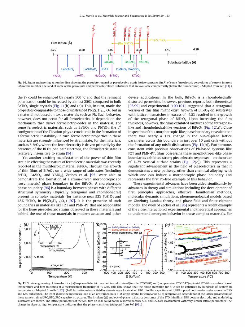
Fig. 10. Strain engineering. A number line showing the pseudotetragonal or pseudocubic a-axis lattice constants (in A) of some ferroelectric perovskites of current interest
(above the number line) and of some of the perovskite and perovskite-related substrates that are available commercially (below the number line). (Adapted from Ref. [91].)
L.W. Martin et al. / Materials Science and Engineering R 68 (2010) 89–133 101
the TC could be enhanced by nearly 500 8C and that the remnantpolarization could be increased by almost 250% compared to bulkBaTiO3 single crystals (Fig. 11(b) and (c)). This, in turn, made theproperties comparable to those of unstrained Pb(ZrxTi1�x)O3, but ina material not based on toxic materials such as Pb. Such behavior,however, does not occur for all ferroelectrics. It depends on themechanism that drives ferroelectric-order in the material. Forsome ferroelectric materials, such as BaTiO3 and PbTiO3, the d0
configuration of the Ti cation plays a crucial role in the formation ofa ferroelectric instability; in turn, ferroelectric properties in thesematerials are strongly influenced by strain state. For the materials,such as BiFeO3, where the ferroelectricity is driven primarily by thepresence of the Bi 6s lone pair electrons, the ferroelectric state isrelatively insensitive to strain [94].
Yet another exciting manifestation of the power of thin filmstrain in effecting the nature of ferroelectric materials was recentlyreported in the multiferroic material BiFeO3. Through the growthof thin films of BiFeO3 on a wide range of substrates (includingSrTiO3, LaAlO3, and YAlO3), Zeches et al. [95] were able todemonstrate the formation of a strain-driven morphotropic (orisosymmetric) phase boundary in the BiFeO3. A morphotropicphase boundary [96] is a boundary between phases with differentstructural symmetry (typically tetragonal and rhombohedral)present in complex materials (for instance near 52% PbZrO3 and48% PbTiO3 in Pb(ZrxTi1�x)O3) [97]. It is the presence of suchboundaries in materials like PZT and PMN-PT that are responsiblefor the huge piezoelectric strains observed in these materials andbehind the use of these materials in modern actuator and other
Fig. 11. Strain engineering of ferroelectrics. (a) In-plane dielectric constant in and strained
temperature and film thickness at a measurement frequency of 10 GHz. This data sho
temperature. (Adapted from Ref. [92].) (b) Polarization-electric field hysteresis loops for s
and GSO substrates. The inset shows the hysteresis loop of an unstrained bulk BTO sing
these same strained SRO/BTO/SRO capacitor structures. The in-plane (//) and out-of-plan
substrates are shown. The lattice parameters of the SRO film on DSO could not be resolv
change in slope at high temperature indicates that the phase transition. (Adapted from
device applications. In the bulk, BiFeO3 is a rhombohedrallydistorted perovskite, however, previous reports, both theoretical[98,99] and experimental [100,101], suggested that a tetragonalversion of this film might exist. Growth of BiFeO3 on substrateswith lattice mismatches in excess of—4.5% resulted in the growthof the tetragonal phase of BiFeO3. Upon increasing the filmthickness, however, the films exhibited mixtures of the tetragonal-like and rhombohedral-like versions of BiFeO3 (Fig. 12(a)). Closeinspection of this morphotropic-like phase boundary revealed thatthere was nearly a 13% change in the out-of-plane latticeparameter across this boundary in just over 10 unit cells withoutthe formation of any misfit dislocations (Fig. 12(b)). Furthermore,consistent with previous observations of Pb-based systems likePZT and PMN-PT, films possessing these morphotropic-like phaseboundaries exhibited strong piezoelectric responses – on the orderof 1–2% vertical surface strains (Fig. 12(c)). This represents asignificant advancement in the field of piezoelectrics in that itdemonstrates a new pathway, other than chemical alloying, withwhich one can induce a morphotropic phase boundary andrepresents the first Pb-free example of this behavior.
These experimental advances have been aided significantly byadvances in theory and simulations including the development offirst principles approaches, effective Hamiltonian methods,molecular dynamic simulations, phenomenological models basedon Ginzburg–Landau theory, and phase-field and finite-elementmodels. The work of Zeches et al. [95] represents a recent exampleof the close interaction of experimental and theoretical approachesto understand emergent behavior in these complex materials. For
(tensile, STO/DSO) and (compressive, STO/LSAT) epitaxial STO films as a function of
ws that the phase transition for STO can be enhanced by hundreds of degrees in
trained BTO thin film capacitors with SRO top and bottom electrodes grown on DSO
le crystal for comparison. (c) Temperature dependence of the lattice parameters of
e (?) lattice constants of the BTO thin films, SRO bottom electrode, and underlying
ed because SRO and DSO are isostructural with very similar lattice parameters. The
Ref. [93].)
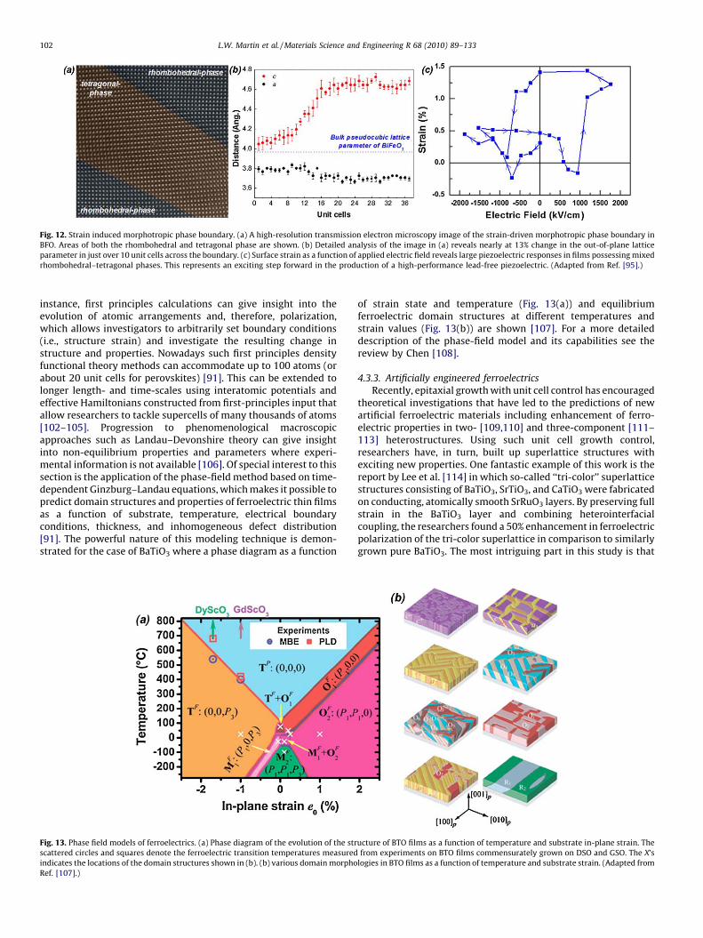
Fig. 12. Strain induced morphotropic phase boundary. (a) A high-resolution transmission electron microscopy image of the strain-driven morphotropic phase boundary in
BFO. Areas of both the rhombohedral and tetragonal phase are shown. (b) Detailed analysis of the image in (a) reveals nearly at 13% change in the out-of-plane lattice
parameter in just over 10 unit cells across the boundary. (c) Surface strain as a function of applied electric field reveals large piezoelectric responses in films possessing mixed
rhombohedral–tetragonal phases. This represents an exciting step forward in the production of a high-performance lead-free piezoelectric. (Adapted from Ref. [95].)
L.W. Martin et al. / Materials Science and Engineering R 68 (2010) 89–133102
instance, first principles calculations can give insight into theevolution of atomic arrangements and, therefore, polarization,which allows investigators to arbitrarily set boundary conditions(i.e., structure strain) and investigate the resulting change instructure and properties. Nowadays such first principles densityfunctional theory methods can accommodate up to 100 atoms (orabout 20 unit cells for perovskites) [91]. This can be extended tolonger length- and time-scales using interatomic potentials andeffective Hamiltonians constructed from first-principles input thatallow researchers to tackle supercells of many thousands of atoms[102–105]. Progression to phenomenological macroscopicapproaches such as Landau–Devonshire theory can give insightinto non-equilibrium properties and parameters where experi-mental information is not available [106]. Of special interest to thissection is the application of the phase-field method based on time-dependent Ginzburg–Landau equations, which makes it possible topredict domain structures and properties of ferroelectric thin filmsas a function of substrate, temperature, electrical boundaryconditions, thickness, and inhomogeneous defect distribution[91]. The powerful nature of this modeling technique is demon-strated for the case of BaTiO3 where a phase diagram as a function
Fig. 13. Phase field models of ferroelectrics. (a) Phase diagram of the evolution of the str
scattered circles and squares denote the ferroelectric transition temperatures measured
indicates the locations of the domain structures shown in (b). (b) various domain morpho
Ref. [107].)
of strain state and temperature (Fig. 13(a)) and equilibriumferroelectric domain structures at different temperatures andstrain values (Fig. 13(b)) are shown [107]. For a more detaileddescription of the phase-field model and its capabilities see thereview by Chen [108].
4.3.3. Artificially engineered ferroelectrics
Recently, epitaxial growth with unit cell control has encouragedtheoretical investigations that have led to the predictions of newartificial ferroelectric materials including enhancement of ferro-electric properties in two- [109,110] and three-component [111–113] heterostructures. Using such unit cell growth control,researchers have, in turn, built up superlattice structures withexciting new properties. One fantastic example of this work is thereport by Lee et al. [114] in which so-called ‘‘tri-color’’ superlatticestructures consisting of BaTiO3, SrTiO3, and CaTiO3 were fabricatedon conducting, atomically smooth SrRuO3 layers. By preserving fullstrain in the BaTiO3 layer and combining heterointerfacialcoupling, the researchers found a 50% enhancement in ferroelectricpolarization of the tri-color superlattice in comparison to similarlygrown pure BaTiO3. The most intriguing part in this study is that
ucture of BTO films as a function of temperature and substrate in-plane strain. The
from experiments on BTO films commensurately grown on DSO and GSO. The X’s
logies in BTO films as a function of temperature and substrate strain. (Adapted from
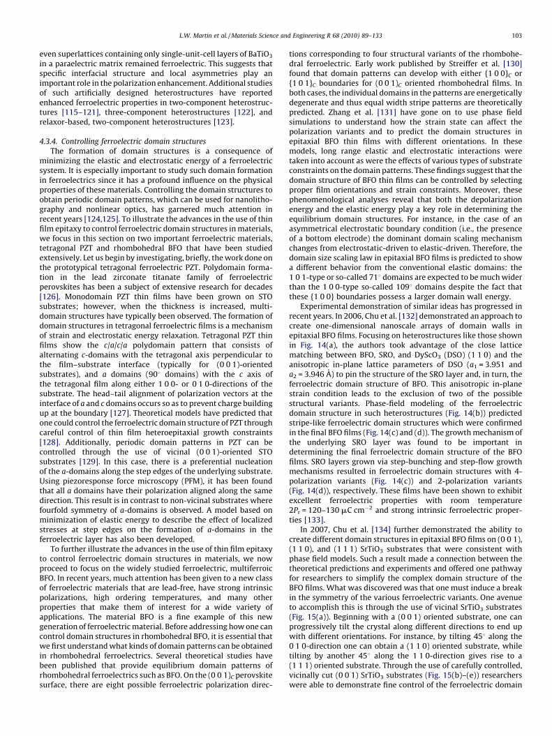
L.W. Martin et al. / Materials Science and Engineering R 68 (2010) 89–133 103
even superlattices containing only single-unit-cell layers of BaTiO3
in a paraelectric matrix remained ferroelectric. This suggests thatspecific interfacial structure and local asymmetries play animportant role in the polarization enhancement. Additional studiesof such artificially designed heterostructures have reportedenhanced ferroelectric properties in two-component heterostruc-tures [115–121], three-component heterostructures [122], andrelaxor-based, two-component heterostructures [123].
4.3.4. Controlling ferroelectric domain structures
The formation of domain structures is a consequence ofminimizing the elastic and electrostatic energy of a ferroelectricsystem. It is especially important to study such domain formationin ferroelectrics since it has a profound influence on the physicalproperties of these materials. Controlling the domain structures toobtain periodic domain patterns, which can be used for nanolitho-graphy and nonlinear optics, has garnered much attention inrecent years [124,125]. To illustrate the advances in the use of thinfilm epitaxy to control ferroelectric domain structures in materials,we focus in this section on two important ferroelectric materials,tetragonal PZT and rhombohedral BFO that have been studiedextensively. Let us begin by investigating, briefly, the work done onthe prototypical tetragonal ferroelectric PZT. Polydomain forma-tion in the lead zirconate titanate family of ferroelectricperovskites has been a subject of extensive research for decades[126]. Monodomain PZT thin films have been grown on STOsubstrates; however, when the thickness is increased, multi-domain structures have typically been observed. The formation ofdomain structures in tetragonal ferroelectric films is a mechanismof strain and electrostatic energy relaxation. Tetragonal PZT thinfilms show the c/a/c/a polydomain pattern that consists ofalternating c-domains with the tetragonal axis perpendicular tothe film–substrate interface (typically for (0 0 1)-orientedsubstrates), and a domains (908 domains) with the c axis ofthe tetragonal film along either 1 0 0- or 0 1 0-directions of thesubstrate. The head–tail alignment of polarization vectors at theinterface of a and c domains occurs so as to prevent charge buildingup at the boundary [127]. Theoretical models have predicted thatone could control the ferroelectric domain structure of PZT throughcareful control of thin film heteroepitaxial growth constraints[128]. Additionally, periodic domain patterns in PZT can becontrolled through the use of vicinal (0 0 1)-oriented STOsubstrates [129]. In this case, there is a preferential nucleationof the a-domains along the step edges of the underlying substrate.Using piezoresponse force microscopy (PFM), it has been foundthat all a domains have their polarization aligned along the samedirection. This result is in contrast to non-vicinal substrates wherefourfold symmetry of a-domains is observed. A model based onminimization of elastic energy to describe the effect of localizedstresses at step edges on the formation of a-domains in theferroelectric layer has also been developed.
To further illustrate the advances in the use of thin film epitaxyto control ferroelectric domain structures in materials, we nowproceed to focus on the widely studied ferroelectric, multiferroicBFO. In recent years, much attention has been given to a new classof ferroelectric materials that are lead-free, have strong intrinsicpolarizations, high ordering temperatures, and many otherproperties that make them of interest for a wide variety ofapplications. The material BFO is a fine example of this newgeneration of ferroelectric material. Before addressing how one cancontrol domain structures in rhombohedral BFO, it is essential thatwe first understand what kinds of domain patterns can be obtainedin rhombohedral ferroelectrics. Several theoretical studies havebeen published that provide equilibrium domain patterns ofrhombohedral ferroelectrics such as BFO. On the (0 0 1)C perovskitesurface, there are eight possible ferroelectric polarization direc-
tions corresponding to four structural variants of the rhombohe-dral ferroelectric. Early work published by Streiffer et al. [130]found that domain patterns can develop with either {1 0 0}C or{1 0 1}C boundaries for (0 0 1)C oriented rhombohedral films. Inboth cases, the individual domains in the patterns are energeticallydegenerate and thus equal width stripe patterns are theoreticallypredicted. Zhang et al. [131] have gone on to use phase fieldsimulations to understand how the strain state can affect thepolarization variants and to predict the domain structures inepitaxial BFO thin films with different orientations. In thesemodels, long range elastic and electrostatic interactions weretaken into account as were the effects of various types of substrateconstraints on the domain patterns. These findings suggest that thedomain structure of BFO thin films can be controlled by selectingproper film orientations and strain constraints. Moreover, thesephenomenological analyses reveal that both the depolarizationenergy and the elastic energy play a key role in determining theequilibrium domain structures. For instance, in the case of anasymmetrical electrostatic boundary condition (i.e., the presenceof a bottom electrode) the dominant domain scaling mechanismchanges from electrostatic-driven to elastic-driven. Therefore, thedomain size scaling law in epitaxial BFO films is predicted to showa different behavior from the conventional elastic domains: the1 0 1-type or so-called 718 domains are expected to be much widerthan the 1 0 0-type so-called 1098 domains despite the fact thatthese {1 0 0} boundaries possess a larger domain wall energy.
Experimental demonstration of similar ideas has progressed inrecent years. In 2006, Chu et al. [132] demonstrated an approach tocreate one-dimensional nanoscale arrays of domain walls inepitaxial BFO films. Focusing on heterostructures like those shownin Fig. 14(a), the authors took advantage of the close latticematching between BFO, SRO, and DyScO3 (DSO) (1 1 0) and theanisotropic in-plane lattice parameters of DSO (a1 = 3.951 anda2 = 3.946 A) to pin the structure of the SRO layer and, in turn, theferroelectric domain structure of BFO. This anisotropic in-planestrain condition leads to the exclusion of two of the possiblestructural variants. Phase-field modeling of the ferroelectricdomain structure in such heterostructures (Fig. 14(b)) predictedstripe-like ferroelectric domain structures which were confirmedin the final BFO films (Fig. 14(c) and (d)). The growth mechanism ofthe underlying SRO layer was found to be important indetermining the final ferroelectric domain structure of the BFOfilms. SRO layers grown via step-bunching and step-flow growthmechanisms resulted in ferroelectric domain structures with 4-polarization variants (Fig. 14(c)) and 2-polarization variants(Fig. 14(d)), respectively. These films have been shown to exhibitexcellent ferroelectric properties with room temperature2Pr = 120–130 mC cm�2 and strong intrinsic ferroelectric proper-ties [133].
In 2007, Chu et al. [134] further demonstrated the ability tocreate different domain structures in epitaxial BFO films on (0 0 1),(1 1 0), and (1 1 1) SrTiO3 substrates that were consistent withphase field models. Such a result made a connection between thetheoretical predictions and experiments and offered one pathwayfor researchers to simplify the complex domain structure of theBFO films. What was discovered was that one must induce a breakin the symmetry of the various ferroelectric variants. One avenueto accomplish this is through the use of vicinal SrTiO3 substrates(Fig. 15(a)). Beginning with a (0 0 1) oriented substrate, one canprogressively tilt the crystal along different directions to end upwith different orientations. For instance, by tilting 458 along the0 1 0-direction one can obtain a (1 1 0) oriented substrate, whiletilting by another 458 along the 1 1 0-direction gives rise to a(1 1 1) oriented substrate. Through the use of carefully controlled,vicinally cut (0 0 1) SrTiO3 substrates (Fig. 15(b)–(e)) researcherswere able to demonstrate fine control of the ferroelectric domain
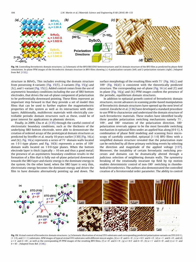
Fig. 14. Controlling ferroelectric domain structures. (a) Schematic of the BFO/SRO/DSO heterostructures and (b) domain structure of the BFO film as predicted by phase-field
simulations. In-plane PFM images of the ferroelectric domain structure in BFO films showing (c) 4-polarization variants (left) and 2-polarization variants (right). (Adapted
from Ref. [132].)
L.W. Martin et al. / Materials Science and Engineering R 68 (2010) 89–133104
structure in BiFeO3. This includes evolving the domain structurefrom possessing 4-variants (Fig. 15(f)), 2-variants (Fig. 15(g) and(h)), and 1-variant (Fig. 15(i)). Added control comes from the use ofasymmetric boundary conditions including the use of SRO bottomelectrodes, that drives the out-of-plane component of polarizationto be preferentially downward pointing. These films represent animportant step forward in that they provide a set of model thinfilms that can be used to further explore the magnetoelectricproperties of this system as well as its interactions with otherlayers. Additionally, multiferroic materials with electrically con-trollable periodic domain structures such as these, could be ofgreat interest for applications in photonic devices.
Finally, in 2009, Chu et al. [135] through the careful control ofelectrostatic boundary conditions, such as the thickness of theunderlying SRO bottom electrode, were able to demonstrate thecreation of ordered arrays of the prototypical domain structures aspredicted by Streiffer et al. nearly 10 years earlier [130] (Fig. 16(a)and (b)). Fig. 16(a) represents a series of 718 domain walls locatedon 1 0 1-type planes and Fig. 16(b) represents a series of 1098domain walls located on 1 0 0-type planes. When the bottomelectrode layer is thick (typically > 10 nm and thus a good metal)the presence of an asymmetric boundary condition results in theformation of a film that is fully out-of-plane polarized downwardtowards the SRO layer and elastic energy is the dominate energy inthe system. On the other hand, when the SRO layer is very thin,electrostatic energy becomes the dominant energy and drives thefilm to have domains alternatively pointing up and down. The
Fig. 15. Vicinal control of ferroelectric domain structures. (a) Schematic illustration of vici
(1 1 0), and (1 1 1) substrates. AFM images of typical vicinal STO substrates with different
a = 38 and b = 458, as well as the corresponding IP-PFM images of the resulting BFO film
b = 458. (Adapted from Ref. [134].)
surface morphology of the resulting films with 718 (Fig. 16(c)) and1098 (Fig. 16(d)) is consistent with the theoretically predictedstructure. The corresponding out-of-plane (Fig. 16 (e) and (f)) andin-plane (Fig. 16(g) and (h)) PFM images confirm the presence ofthe periodic, equilibrium domain structures.
In addition to epitaxial growth control of ferroelectric domainstructures, recent advances in scanning probe-based manipulationof ferroelectric domain structures have opened up the next level ofcontrol. Zavaliche et al. [136] have developed a standard procedureto use PFM to characterize and understand the domain structure ofsuch ferroelectric materials. These studies have identified locallythree possible polarization switching mechanisms namely 718,1098, and 1808 rotations of the polarization direction. 1808polarization reversals appear to be the most favorable switchingmechanism in epitaxial films under an applied bias along [0 0 1]. Acombination of phase field modeling and scanning force micro-scopy of carefully controlled, epitaxial [1 1 0] BFO films with asimplified domain structure revealed that the polarization statecan be switched by all three primary switching events by selectingthe direction and magnitude of the applied voltage [137].Moreover, the instability of certain ferroelastic switching pro-cesses and domains can be dramatically altered through ajudicious selection of neighboring domain walls. The symmetrybreaking of the rotationally invariant tip field by tip motionenables deterministic control of non-1808 switching in rhombo-hedral ferroelectrics. The authors also demonstrated the controlledcreation of a ferrotorroidal order parameter. The ability to control
nal STO substrates and corresponding predicted polarization variants on STO (0 0 1),
miscut angles, (b) a = 08 and b = 08, (c) a = 0.58 and b = 08, (d) a = 18 and b = 08, and (d)
s, (f) a = 08 and b = 08, (g) a = 0.58 and b = 08, (h) a = 18 and b = 08, and (i) a = 38 and
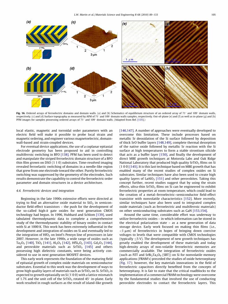
Fig. 16. Ordered arrays of ferroelectric domains and domain walls. (a) and (b) Schematics of equilibrium structure of an ordered array of 718 and 1098 domain walls,
respectively. (c) and (d) Surface topography as measured by AFM of 718 and 1098 domain walls samples, respectively. Out-of-plane (e) and (f) as well as in-plane (g) and (h)
PFM images for samples possessing ordered arrays of 718 and 1098 domain walls. (Adapted from Ref. [135].)
L.W. Martin et al. / Materials Science and Engineering R 68 (2010) 89–133 105
local elastic, magnetic and torroidal order parameters with anelectric field will make it possible to probe local strain andmagnetic ordering, and engineer various magnetoelectric, domain-wall-based and strain-coupled devices.
For eventual device applications, the use of a coplanar epitaxialelectrode geometry has been proposed to aid in controllingmultiferroic switching in BFO [138]. PFM has been used to detectand manipulate the striped ferroelectric domain structure of a BFOthin film grown on DSO (1 1 0) substrates. Time-resolved imagingrevealed ferroelastic switching of domains in a needle-like regionthat grew from one electrode toward the other. Purely ferroelectricswitching was suppressed by the geometry of the electrodes. Suchresults demonstrate the capability to control the ferroelectric orderparameter and domain structures in a device architecture.
4.4. Ferroelectric devices and integration
Beginning in the late 1990s extensive efforts were directed attrying to find an alternative oxide material to SiO2 in semicon-ductor field-effect transistors – the push for the development ofthe so-called high-k gate oxides for next generation CMOStechnology had begun. In 1996, Hubbard and Schlom [139], usedtabulated thermodynamic data to complete a comprehensivestudy of the thermodynamic stability of binary oxides in contactwith Si at 1000 K. This work has been extremely influential in thedevelopment and integration of oxides on Si and eventually led tothe integration of HfO2 on Intel’s Penryn line of processors in late2007. However, in the late 1990s, a wide range of oxides such asTa2O5 [140], TiO2 [141], Al2O3 [142], HfSixOy [143], Gd2O3 [144],and perovskite materials such as SrTiO3 [145] and otherspossessing high dielectric constants, were being actively con-sidered to use in next generation MOSFET devices.
This early work represents the foundation of the maturing fieldof epitaxial growth of complex oxide materials on semiconductorsubstrates. Essential to this work was the development of ways togrow high quality layers of materials such as SrTiO3 on Si. SrTiO3 isexpected to growth epitaxially on Si (1 0 0) with a lattice mismatchof 1.7% and the unit cell of the SrTiO3 rotated 458 in-plane. Earlywork resulted in rough surfaces as the result of island-like growth
[146,147]. A number of approaches were eventually developed toovercome this limitation. These include processes based onmetallic Sr deoxidation of the Si surface followed by depositionof thick SrO buffer layers [148,149], complete thermal desorptionof the native oxide followed by metallic Sr reaction with the Sisurface at high temperatures to form a stable strontium silicidethat acts as a buffer layer [150], and finally the development ofdirect MBE growth techniques at Motorola Labs and Oak RidgeNational Laboratory that produced high quality SrTiO3 films on Si(1 0 0) [145]. It is this last technique based on MBE growth that hasenabled many of the recent studies of complex oxides on Sisubstrates. Similar techniques have also been used to create highquality layers of LaAlO3 [151] and other perovskites. Taking thisconcept further, recent studies suggest that by using the straineffects, ultra-thin SrTiO3 films on Si can be engineered to exhibitferroelectric properties at room temperature, which could lead tothe creation of a metal–ferroelectric–semiconductor field-effecttransistor with nonvolatile characteristics [152]. More recently,similar techniques have also been used to integrated complexoxide materials (such as ferroelectric and multiferroic materials)on other semiconducting substrates such as GaN [153,154].
Around the same time, considerable effort was underway toutilize ferroelectric oxides – in which information can be stored inthe electrical polarization state – as a new generation of datastorage device. Early work focused on making thin films (i.e.,<1 mm) of ferroelectrics in hopes of bringing down coercivevoltages to levels that were compatible with CMOS technologies(typically �5 V). The development of new growth techniques hasgreatly enabled the development of these materials and todayhigh-density arrays of non-volatile ferroelectric memories arecommercially available. The integration of ferroelectric oxides(such as PZT and SrBi2Ta2O9 (SBT)) on Si for nonvolatile memoryapplications (FRAM’s) preceded the studies of oxide heteroepitaxy(Fig. 17); however, the key materials innovations in the field offerroelectric capacitors directly benefited from the concepts ofheteroepitaxy. It is fair to state that the critical roadblocks to theimplementation of a commercial FRAM technology were overcomeby the fundamental studies that involved the use of conductingperovskite electrodes to contact the ferroelectric layers. This
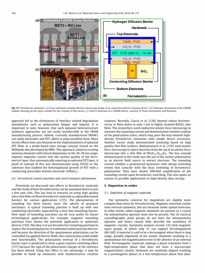
Fig. 17. Ferroelectric memories. (a) Cross-sectional scanning electron microscopy image of an actual ferroelectric memory device. (b) Schematic illustration of the FeRAM
module showing all the layers needed for the creation of this device. (c) Artist’s depiction of a FeRAM device, courtesy of Texas Instruments and Ramtron.
L.W. Martin et al. / Materials Science and Engineering R 68 (2010) 89–133106
approach led to the elimination of interface related degradationmechanisms such as polarization fatigue and imprint. It isimportant to note, however, that such epitaxial heterostructuresynthesis approaches are not easily transferrable to the FRAMmanufacturing process. Indeed, currently manufactured FRAM’suse oxide electrodes and PZT, albeit in polycrystalline form. Morerecent efforts have also focused on the implementation of epitaxialPZT films in a probe-based data storage concept (based on theMillipede idea developed by IBM). This approach, aimed at creatingmemory elements with lateral dimensions in the 20–50 nm range,requires exquisite control over the surface quality of the ferro-electric layer, thus automatically requiring an epitaxial PZT layer. Aproof of concept of this was demonstrated using STO/Si as thesubstrate that enabled the heteroepitaxial growth of PZT with aconducting perovskite bottom electrode (SrRuO3).
4.5. Ferroelectric tunnel junctions and novel transport phenomena
Previously we discussed size effects in ferroelectric materialsand the study of how ferroelectricity can be sustained down to justa few unit cells. This has lead to research on using high qualityultra-thin films of these ferroelectric materials as adjustable tunnelbarriers for various applications [155]. The phenomenon oftunneling has been known since the advent of quantummechanics. A typical tunneling junction is built up with twoconducting electrodes separated by a very thin insulating barrier.New types of tunneling junctions can be very useful for futuretechnological applications. For example, magnetic tunnelingjunctions have shown the potential application in spintronicdevices [156]. The idea is to use ferroelectric tunneling junctions toreplace the insulating barrier in traditional tunnel junction devices,and because the direction of the spontaneous polarization can becontrolled via applied electric fields, this construction could enablenew functionality. The polarization reversal of a ferroelectricbarrier layer is predicted to show a giant resistive switching effect[157] because the sign of the polarization charges at the interfacehas been altered. Using this effect to our advantage, it may bepossible to build up memories with nondestructive resistive
readouts. Recently, Garcia et al. [158] showed robust ferroelec-tricity in films down to only 1 nm in highly strained BaTiO3 thinfilms. The researchers used conductive atomic force microscopy tomeasure the tunneling current and demonstrated resistive readoutof the polarization states, which may pave the way towards high-density ferroelectric memories with simple device structures.Another recent study demonstrated tunneling based on highquality thin film surfaces. Maksymovych et al. [159] used atomicforce microscopy to inject electrons from the tip of an atomic forcemicroscope into a thin film of Pb(Zr0.2Ti0.8)O3. The key conceptdemonstrated in this study was the use of the surface polarizationas an electric field source to extract electrons. The tunnelingcurrent exhibits a pronounced hysteresis with abrupt switchingevents that coincide with the local switching of ferroelectricpolarization. They have shown 500-fold amplification of thetunneling current upon ferroelectric switching. This also opens anavenue to possible applications in high-density data storage.
5. Magnetism in oxides
5.1. Definition of magnetic materials
The symmetry concerns for magnetism are slightly morecomplex than those for ferroelectricity. Magnetic materials violatetime reversal symmetry, but are invariant under spatial inversion,in other words, when magnetic moments are present in a crystalthe antisymmetry operator must also be present. The 32 classicalcrystallographic point groups do not have the antisymmetryoperator and hence cannot fully describe the symmetry ofmagnetic crystals. Symmetry analysis reveals 122 total magneticspace groups of which only 31 can support ferromagnetism[60,160]. A material is said to be a ferromagnet when there is longrange, parallel alignment of the atomic moments resulting in aspontaneous net magnetization even in the absence of an externalfield. Ferromagnetic materials undergo a phase transition from ahigh-temperature phase that does not have a macroscopicmagnetization (atomic moments are randomly aligned resultingin a paramagnetic phase) to a low-temperature phase that does.
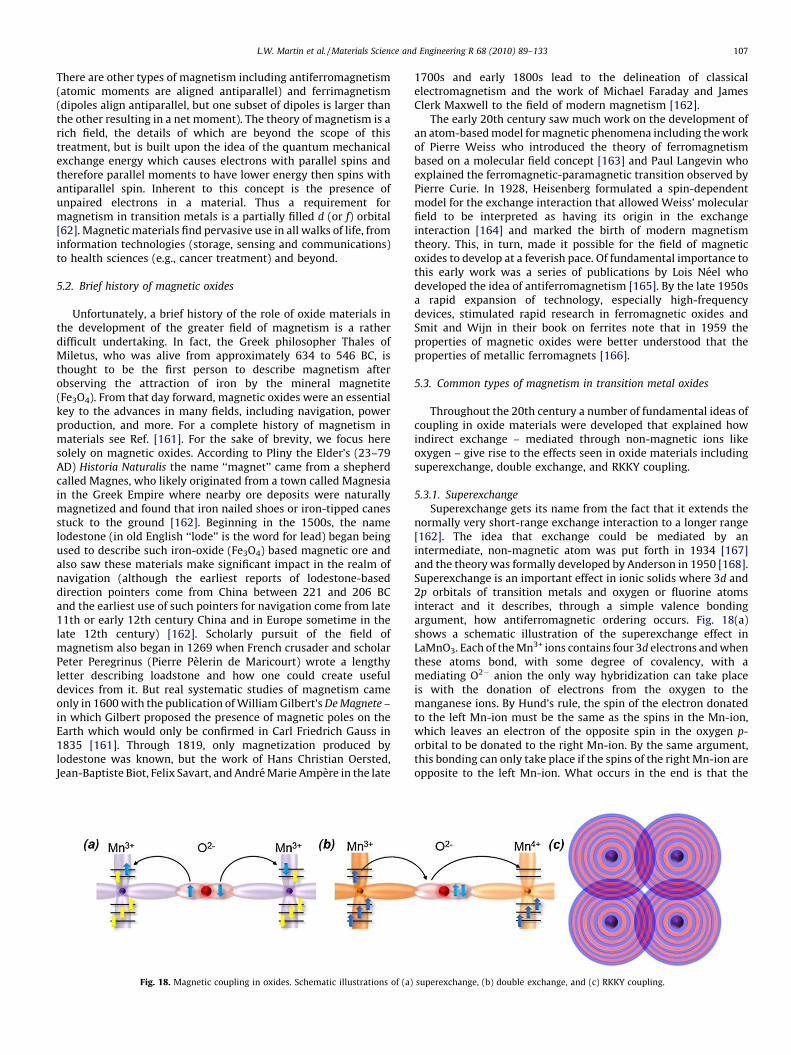
L.W. Martin et al. / Materials Science and Engineering R 68 (2010) 89–133 107
There are other types of magnetism including antiferromagnetism(atomic moments are aligned antiparallel) and ferrimagnetism(dipoles align antiparallel, but one subset of dipoles is larger thanthe other resulting in a net moment). The theory of magnetism is arich field, the details of which are beyond the scope of thistreatment, but is built upon the idea of the quantum mechanicalexchange energy which causes electrons with parallel spins andtherefore parallel moments to have lower energy then spins withantiparallel spin. Inherent to this concept is the presence ofunpaired electrons in a material. Thus a requirement formagnetism in transition metals is a partially filled d (or f) orbital[62]. Magnetic materials find pervasive use in all walks of life, frominformation technologies (storage, sensing and communications)to health sciences (e.g., cancer treatment) and beyond.
5.2. Brief history of magnetic oxides
Unfortunately, a brief history of the role of oxide materials inthe development of the greater field of magnetism is a ratherdifficult undertaking. In fact, the Greek philosopher Thales ofMiletus, who was alive from approximately 634 to 546 BC, isthought to be the first person to describe magnetism afterobserving the attraction of iron by the mineral magnetite(Fe3O4). From that day forward, magnetic oxides were an essentialkey to the advances in many fields, including navigation, powerproduction, and more. For a complete history of magnetism inmaterials see Ref. [161]. For the sake of brevity, we focus heresolely on magnetic oxides. According to Pliny the Elder’s (23–79AD) Historia Naturalis the name ‘‘magnet’’ came from a shepherdcalled Magnes, who likely originated from a town called Magnesiain the Greek Empire where nearby ore deposits were naturallymagnetized and found that iron nailed shoes or iron-tipped canesstuck to the ground [162]. Beginning in the 1500s, the namelodestone (in old English ‘‘lode’’ is the word for lead) began beingused to describe such iron-oxide (Fe3O4) based magnetic ore andalso saw these materials make significant impact in the realm ofnavigation (although the earliest reports of lodestone-baseddirection pointers come from China between 221 and 206 BCand the earliest use of such pointers for navigation come from late11th or early 12th century China and in Europe sometime in thelate 12th century) [162]. Scholarly pursuit of the field ofmagnetism also began in 1269 when French crusader and scholarPeter Peregrinus (Pierre Pelerin de Maricourt) wrote a lengthyletter describing loadstone and how one could create usefuldevices from it. But real systematic studies of magnetism cameonly in 1600 with the publication of William Gilbert’s De Magnete –in which Gilbert proposed the presence of magnetic poles on theEarth which would only be confirmed in Carl Friedrich Gauss in1835 [161]. Through 1819, only magnetization produced bylodestone was known, but the work of Hans Christian Oersted,Jean-Baptiste Biot, Felix Savart, and Andre Marie Ampere in the late
Fig. 18. Magnetic coupling in oxides. Schematic illustrations of (a)
1700s and early 1800s lead to the delineation of classicalelectromagnetism and the work of Michael Faraday and JamesClerk Maxwell to the field of modern magnetism [162].
The early 20th century saw much work on the development ofan atom-based model for magnetic phenomena including the workof Pierre Weiss who introduced the theory of ferromagnetismbased on a molecular field concept [163] and Paul Langevin whoexplained the ferromagnetic-paramagnetic transition observed byPierre Curie. In 1928, Heisenberg formulated a spin-dependentmodel for the exchange interaction that allowed Weiss’ molecularfield to be interpreted as having its origin in the exchangeinteraction [164] and marked the birth of modern magnetismtheory. This, in turn, made it possible for the field of magneticoxides to develop at a feverish pace. Of fundamental importance tothis early work was a series of publications by Lois Neel whodeveloped the idea of antiferromagnetism [165]. By the late 1950sa rapid expansion of technology, especially high-frequencydevices, stimulated rapid research in ferromagnetic oxides andSmit and Wijn in their book on ferrites note that in 1959 theproperties of magnetic oxides were better understood that theproperties of metallic ferromagnets [166].
5.3. Common types of magnetism in transition metal oxides
Throughout the 20th century a number of fundamental ideas ofcoupling in oxide materials were developed that explained howindirect exchange – mediated through non-magnetic ions likeoxygen – give rise to the effects seen in oxide materials includingsuperexchange, double exchange, and RKKY coupling.
5.3.1. Superexchange
Superexchange gets its name from the fact that it extends thenormally very short-range exchange interaction to a longer range[162]. The idea that exchange could be mediated by anintermediate, non-magnetic atom was put forth in 1934 [167]and the theory was formally developed by Anderson in 1950 [168].Superexchange is an important effect in ionic solids where 3d and2p orbitals of transition metals and oxygen or fluorine atomsinteract and it describes, through a simple valence bondingargument, how antiferromagnetic ordering occurs. Fig. 18(a)shows a schematic illustration of the superexchange effect inLaMnO3. Each of the Mn3+ ions contains four 3d electrons and whenthese atoms bond, with some degree of covalency, with amediating O2� anion the only way hybridization can take placeis with the donation of electrons from the oxygen to themanganese ions. By Hund’s rule, the spin of the electron donatedto the left Mn-ion must be the same as the spins in the Mn-ion,which leaves an electron of the opposite spin in the oxygen p-orbital to be donated to the right Mn-ion. By the same argument,this bonding can only take place if the spins of the right Mn-ion areopposite to the left Mn-ion. What occurs in the end is that the
superexchange, (b) double exchange, and (c) RKKY coupling.

L.W. Martin et al. / Materials Science and Engineering R 68 (2010) 89–133108
oxygen-mediate bonding leads to a collective antiparallel spinalignment of nearest neighbor Mn-ions.
5.3.2. Double exchange
Double exchange, which was first proposed by Zener in 1951[169], begins to change the nature of magnetic coupling inmaterials like LaMnO3 if one dopes in materials like Sr or Ca on theLa-site, creating a mixed valence compound. Double exchangedescribes the magneto-conductive properties of these mixedvalence compounds and delineates the mechanism for hoppingof an electron from one site to another through the mediatingoxygen atom. Again, because the O2� ion has full p-orbitals, themovement from one ion through O2� to another ion is done in twosteps. Let us explore this idea for the case of the widely studiedoxide ferromagnet La0.7Sr0.3MnO3 which has Mn3+ and Mn4+ ions(Fig. 18(b)). Assuming the ligand field is relatively small and we fillthe 3d orbitals following Hund’s rules the Mn3+ and Mn4+ ions arefilled with electrons as shown with the dark blue arrows. In suchmaterials, electron conduction proceeds by this double stepprocess by which one of the electrons on the Mn-sites jumpsback and forth across the oxygen. The electron is thus delocalizedover the entire M–O–M group and the metal atoms are said to be ofmixed valency. This is aided by the fact that spin-flips are notallowed in electron hopping processes and thus it is moreenergetically favorable if the magnetic structure of the two Mn-ions is identical; therefore, ferromagnetic alignment of moments isachieved.
5.3.3. RKKY coupling
The final type of exchange we will discuss here is RKKYexchange. Unlike the previous two examples, RKKY exchange(named after the work of Ruderman and Kittel [170], Kasuya [171],and Yosida [172]) is not based on the relationship betweenbonding and magnetism, but instead is the concept that a localmoment can induce a spin polarization in a surroundingconduction electron sea. Such studies showed that the spinpolarization of the conduction electrons oscillates in sign as afunction of distance from the localized moment and this spininformation can be carried over relatively long distances(Fig. 18(c)). Such coupling has been proposed to explain couplingin dilute magnetic semiconductor systems where magnetic ionsare too far apart to interact with each other directly and the sign ofthis coupling depends on the distance between magnetic ions.
5.4. Modern magnetic oxides
Since 1950 a number of magnetic oxides have dominated thelandscape of solid state physics research. In this section we willinvestigate two of these systems: ferrites and manganites.
5.4.1. Ferrites
The ferrites include the entire family of Fe-containing oxidessuch as the spinels (AFe2O4), garnets (AFe5O12), hexaferrites(AFe12O19), and orthoferrites (RFeO3, where R is one or more ofthe rare-earth elements). In the past, ferrites have been used inapplications as diverse as transformer cores [173] and microwavemagnetic devices [174] to magneto-optic data storage materials[175] and flux guides and sensors [176]. In this section we willfocus primarily on spinel ferrites as they have received muchrecent attention. The recent push with these materials has been tocreate high quality thin films of these complex materials to enablebetter understanding of structure–property relationships and toenable the creation of novel new devices based on the intriguingproperties of these materials. Considerable effort has beenundertaken to achieve bulk-like properties in ferrite thin filmsand because of the rather complex chemical nature of these
materials careful control of strain effects, growth conditions, andpost-annealing treatments are needed to achieve high qualitysamples. In fact, recent theoretical studies of the spinal materials inparticular point to the delicate nature of these materials as theelectronic structure is strongly dependent on cationic order/disorder in these materials [177]. In some cases, a half-metalliccharacter is expect and this, combined with the high Curietemperatures of these materials, makes them of great interest aselectrodes in magnetic tunnel junctions [178] and spintronicdevices. Additionally, the spinel ferrites have become quitepopular in the study of composite multiferroic heterostructures.Here we will investigate briefly the work on epitaxial films of thematerials Fe3O4, NiFe2O4, and CoFe2O4. For a detailed review ofspinel ferrite thin films see Ref. [179].
5.4.1.1. Fe3O4. Fe3O4 or magnetite is one of the oldest knownmagnetic materials and has been extensively studied over theyears [180], yet it has enjoyed a rejuvenation in interest driven bythe possibility of utilizing the half-metallic nature of the materialin magnetic multilayer devices. Band structure calculationssuggest that the majority spin electrons in Fe3O4 are semicon-ducting with a sizable energy-gap and that the minority spins aremetallic in nature [181]. Magnetite is the half-metal with thehighest known Curie temperature (�858 K). Fe3O4 has also beenstudied because it undergoes an interesting first-order metal–insulator phase transition known as the Verwey transition [182]at 120 K where the Fe3O4 undergoes a structural transition fromcubic to monoclinic [183] structure that is accompanied by adramatic increase in resistivity [184] and decrease in magneticmoment. Strong debate about the fundamental mechanisms forthis transition are still ongoing – especially discussion of thelocalized or delocalized nature of 3d electrons in this system[162].
Driven by the desire to incorporate this material into magneticdevices, epitaxial growth of Fe3O4 has been achieved on (0 0 1)MgO substrates using a wide variety of deposition techniques.Pulsed laser deposition growth with substrate temperaturebetween 200 and 500 8C has yielded good, bulk-like properties[185–190]. A comparison of magnetic properties for bulk Fe3O4
and various thin films is shown in Fig. 19(a) and shows that carefulattention must be given to materials synthesis to achieve bulk-likeproperties in these films. Detailed studies of magnetoresistance[187,191,192] as well as the study of magnetic devices, such asmagnetic tunnel junctions based on Fe3O4 [193–196] have alsobeen completed.
5.4.1.2. NiFe2O4. Nickel ferrite or NiFe2O4, unlike Fe3O4, has asizeable gap in the majority spins and a smaller one in the minorityspins resulting in an insulating state. Epitaxial films of NiFe2O4
have been grown via pulsed laser deposition on c-plane sapphire at900 8C and high oxygen pressures [197]. Other routes to createhigh quality films of NiFe2O4 include the use of buffered spinelsubstrates [198]. Studies of such epitaxial films, however, revealedanomalous magnetic behavior including diminished magnetiza-tion and an anomalous approach to saturation for films grown inthe range of 400–700 8C [199]. Over the years it has been shownthat post-growth anneals at 1000 8C reduced the anomalousmagnetic behavior of these NiFe2O4 films (Fig. 19(b)). More recentinvestigations into ultrathin films of NiFe2O4 on SrTiO3 (0 0 1)substrates has shown that, under the appropriate growthconditions, epitaxial stabilization leads to the formation of aspinel phase with distinctly different magnetic and electronicproperties – including magnetic moments that are enhanced bynearly 250% and metallic character – that results from ananomalous distribution of Fe and Ni cations among the A and B
sites that occurs during non-equilibrium growth [200].
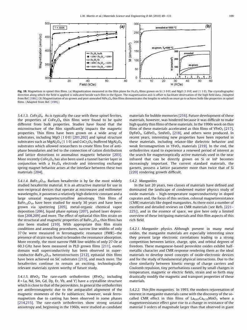
Fig. 19. Magnetism in spinel thin films. (a) Magnetization measured in the film plane for Fe3O4 films grown on Si (1 0 0) and MgO (1 0 0) and (1 1 0). The crystallographic
direction along which the field is applied is indicated beside each film in the figure. The magnetization axis is offset to facilitate observation of the high field data. (Adapted
from Ref. [186].) (b) Magnetization of as-grown and post-annealed NiFe2O4 thin films demonstrates the lengths to which on must go to achieve bulk-like properties in spinel
films. (Adapted from Ref. [199].)
L.W. Martin et al. / Materials Science and Engineering R 68 (2010) 89–133 109
5.4.1.3. CoFe2O4. As is typically the case with these spinel ferrites,the properties of CoFe2O4 thin films were found to be quitedifferent from bulk properties. Studies have found that themicrostructure of the film significantly impacts the magneticproperties. Thin films have been grown on a wide array ofsubstrates, including MgO (1 0 0) [201,202] and spinal structuresubstrates such as MgAl2O4 (1 1 0) and CoCr2O4-buffered MgAl2O4
substrates which allowed researchers to create films free of anti-phase boundaries and led to the connection of cation distributionand lattice distortions to anomalous magnetic behavior [203].More recently CoFe2O4 has also been used a tunnel barrier layer inconjunction with a Fe3O4 electrode and interesting exchangespring magnet behavior arises at the interface between these twomaterials [204].
5.4.1.4. BaFe12O19. Barium hexaferrite is by far the most widelystudied hexaferrite material. It is an attractive material for use innon-reciprocal devices that operate at microwave and millimeterwavelengths, it possesses a relatively high dielectric constant and alarge uniaxial magnetocrystalline anisotropy. Thin films ofBaFe12O19 have been studied for nearly 30 years and have beengrown via sputtering [205], metal-organic chemical vapordeposition [206], liquid phase epitaxy [207], pulsed laser deposi-tion [208,209] and more. The effect of epitaxial thin film strain onthe structural and magnetic properties of BaFe12O19 thin films hasalso been studied [210]. With appropriate thin film strainconditions and annealing procedures, narrow line widths of only37 Oe were measured in ferromagnetic resonance (FMR)—thepresence of strain was found to broaden the resonance absorption.More recently, the most narrow FMR line-widths of only 27 Oe at60.3 GHz have been measured in PLD grown films [211], exoticdomain wall superconductivity has been observed in super-conductor-BaFe12O19 heterostructures [212], epitaxial thin filmshave been achieved on SiC substrates [213], and much more. Thehexaferrites continue to remain an exciting, technologicallyrelevant materials system worthy of future study.
5.4.1.5. RFeO3. The rare-earth orthoferrites (RFeO3, includingR = La, Nd, Sm, Gd, Dy, Er, Yb, and Y) have a crystalline structurewhich is close to that of the perovskites. In general the orthoferritesare antiferromagnetic due to the antiparallel alignment of themagnetic moments of the Fe sublattices; however, weak ferro-magnetism due to canting has been observed in some phases[214,215]. The rare-earth orthoferrites show strong uniaxialanisotropy and, beginning in the 1960s, were studied as candidate
materials for bubble memories [216]. Future development of thesematerials, however, was hindered because it was difficult to makehigh quality thin films of these materials. In the 1990s work on thinfilms of these materials accelerated as thin films of YFeO3 [217],DyFeO3, GdFeO3, SmFeO3 [218], and others were produced. Inrecent years, interesting new properties have been reported inthese materials, including relaxor-like dielectric behavior andweak ferromagnetism in YFeO3 materials [219]. In the end, theorthoferrites stand to experience a renewed period of interest asthe search for magnetooptically active materials used in the nearinfrared that can be directly grown on Si or InP becomesincreasingly important. The current standard materials, thegarnets, possess a lattice parameter more than twice that of Si[220] rendering growth difficult.
5.4.2. Manganites
In the last 20 years, two classes of materials have defined anddominated the landscape of condensed matter physics study ofoxide materials – high-temperature superconductivity in dopedcuprates and, the focus of this section, colossal magnetoresistance(CMR) materials like doped manganites. As there exist a number ofexcellent and detailed reviews on CMR materials (see Refs. [221–225]), and in the essence of space, we give here only a limitedoverview of these intriguing materials and thin film aspects of thisrich field.
5.4.2.1. Manganite physics. Although present in many metaloxides, the manganite materials are especially interesting sincethey present large electronic correlations leading to a strongcompetition between lattice, charge, spin, and orbital degrees offreedom. These manganese-based perovskite oxides exhibit half-metallic character and CMR response rendering them as the idealmaterials to develop novel concepts of oxide-electronic devicesand for the study of fundamental physical interactions. Due to theclose similarity between kinetic energy of charge carriers andCoulomb repulsion, tiny perturbations caused by small changes intemperature, magnetic or electric fields, strain and so forth maydrastically modify the magnetic and transport properties of thesematerials.
5.4.2.2. Thin film manganites. In 1993, the modern rejuvenation ofinterest in manganite materials came with the discovery of the so-called CMR effect in thin films of La0.67Ca0.33MnO3 where amagnetoresistance effect gave rise to a change in resistance of thematerial 3 orders of magnitude larger than that observed in giant
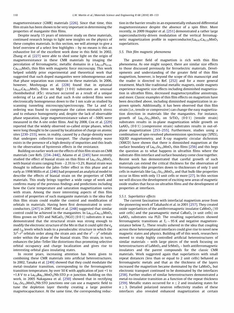
L.W. Martin et al. / Materials Science and Engineering R 68 (2010) 89–133110
magnetoresistance (GMR) materials [226]. Since that time, thinfilm strain has been shown to be very important in determining theproperties of manganite thin films.
Despite nearly 15 years of intensive study on these materials,continued research brings to light new insights on the physics ofthese complex materials. In this section, we will attempt to give abrief overview of a select few highlights – by no means is this anexhaustive list of the excellent work done in this field. In 2002,Zhang et al. [227] were able to shed some light on the origin ofmagnetoresistance in these CMR materials by imaging thepercolation of ferromagnetic, metallic domains in a La0.33Pr0.34-
Ca0.33MnO3 thin film with magnetic force microscopy. This workhelped solidify prior experimental and theoretical work thatsuggested that such doped manganites were inhomogeneous andthat phase separation was common in these materials. In 2006,however, Moshnyaga et al. [228] found that in epitaxialLa0.67Ca0.33MnO3 films on MgO (1 0 0) substrates an unusualrhombohedral ðR3cÞ structure occurred as a result of a uniqueordering of La and Ca and that such A-site ordered films wereelectronically homogeneous down to the 1 nm scale as studied byscanning tunneling microscopy/spectroscopy. The La and Caordering was found to compensate the cation mismatch stressand to enhance homogeneity and, despite the lack of observablephase separation, large magnetoresistance values of �500% weremeasured in the A-site order films. And by 2008, Cox et al. [229]reported that the widely observed so-called stripe phases, whichwere long thought to be caused by localization of charge on atomicsites [230–233], were, in reality, caused by a charge-density wavethat undergoes collective transport. The charge-density waveexists in the presence of a high density of impurities and this leadsto the observation of hysteresis effects in the resistance.
Building on earlier work on the effects of thin film strain on CMRmaterials (see Refs. [234–244]), Adamo et al. [245] have recentlystudied the effect of biaxial strain on thin films of La0.7Sr0.3MnO3
with biaxial strains ranging from�2.3% to +3.2%. Biaxial strain wasthought to influence the Jahn–Teller effect in this phase and asearly as 1998 Millis et al. [246] had proposed an analytical model todescribe the effects of biaxial strain on the properties of CMRmaterials. This study brings together a wide range of work andconfirms many of the previous findings and predictions includinghow the Curie temperature and saturation magnetization varieswith strain. Among the more interesting aspects of thin filmcontrol of properties of such manganite materials is the idea thatthin film strain could enable the control and modification oforbitals in materials. Having been first demonstrated in semi-conductors, [247] in 2007 Abad et al. [248] suggested that similarcontrol could be achieved in the manganites. In La0.67Ca0.33MnO3
films grown on STO and NdGaO3 (NGO) (0 0 1) substrates it wasdemonstrated that the structural strain was strong enough tomodify the electronic structure of the Mn in that it could split the eg
and t2g levels which leads to a pseudocubic structure in which the3z2–r2 orbitals order along the strain axis and the x2 � y2 orbitalsorder within the plane of the biaxial strain. This strain, in turn,enhances the Jahn–Teller like distortions thus promoting selectiveorbital occupancy and charge localization and gives rise tointeresting orbital glass insulating states.
In recent years, increasing attention has been given tocombining these CMR materials into artificial heterostructures.In 2002, Tanaka et al. [249] showed that they could modulate themetal–insulator transition, corresponding to the ferromagnetictransition temperature, by over 50 K with application of just +1 to+1.8 V to a La0.9Ba0.1MnO3/Nb:STO p–n junction. Building on thiswork, in 2005 Nakagawa et al. [250] showed that in rectifyingLa0.7Sr0.3MnO3/Nb:STO junctions one can use a magnetic field totune the depletion layer thereby creating a large positivemagnetocapacitance. At the same time, the corresponding reduc-
tion in the barrier results in an exponentially enhanced differentialmagnetoresistance despite the absence of a spin filter. Morerecently, in 2009 Hoppler et al. [251] demonstrated a rather largesuperconductivity-driven modulation of the vertical ferromag-netic magnetization profile in superconductor/La0.67Ca0.33MnO3
superlattices.
5.5. Thin film magnetic phenomena
The greater field of magnetism is rich with thin filmphenomena. As one might suspect, there are similar size effectsto those discussed previously for ferroelectric materials. Devel-opments and understanding of the greater field of thin filmmagnetism, however, is beyond the scope of this manuscript andthe reader is directed to Ref. [252] and for a more generaltreatment. Much like traditional metallic magnets, oxide magnetsexperience magnetic size effects including diminished magnetiza-tion in ultrathin films, decreased magnetocrystalline anisotropy,and more. Classic examples of thin film effects on magnetism havebeen described above, including diminished magnetization in as-grown spinels. Additionally, it has been observed that thin filmstrain (i.e., tensile or compressive) can change the easy magnetiza-tion direction in materials like the manganites. For instance,growth of La0.7Sr0.3MnO3 on SrTiO3 (0 0 1) (tensile strain)substrates results in in-plane magnetization while growth onLaAlO3 (0 0 1) (compressive strain) substrates results in out-of-plane magnetization [253–255]. Furthermore, studies using acombination of spin-resolved photoemission spectroscopy (SPES),SQUID magnetometry, and X-ray magnetic circular dichroism(XMCD) have shown that there is diminished magnetism at thesurface boundary of La0.7Sr0.3MnO3 thin films [256] and this begsthe question as to what happens in ultrathin films where thesubstrate-film interface and surface boundary come close together.Recent work has demonstrated that careful growth of suchmaterials can extend the critical thickness for the observation offerromagnetic-like properties down to thicknesses of only 3 unitcells in materials like La0.7Sr0.3MnO3, and that bulk-like propertiesoccur in films with only 13 unit cells or more [27]. In this sectionwe will discuss the development of exciting new areas of magneticoxide studies that focus on ultrathin films and the development ofproperties at interfaces.
5.5.1. Superlattice effects
The current fascination with interfacial magnetism arose fromthe pioneering work of Takahashi et al. in 2001 [257]. They createdoxide superlattices of the antiferromagnetic insulator CaMnO3 (10unit cells) and the paramagnetic metal CaRuO3 (n unit cells) onLaAlO3 substrates via PLD. The resulting superlattices showedferromagnetic transitions at TC � 95 K and negative magnetore-sistance below TC. These results ushered in the idea that couplingacross these heteroepitaxial interfaces could give rise to novel newmagnetic states and physics. Building off of this work, researchersmoved to study highly controlled artificial heterostructures ofsimilar materials – with large pieces of the work focusing onheterostructures of LaMnO3 and SrMnO3 – both antiferromagneticinsulators and the parent compounds for the classic CMRmaterials. Work suggested again that superlattices with smallrepeat distances (less than or equal to 2 unit cells) behaved asferromagnetic metals and that as the thickness of the layersincreased the magnetism became dominated by the LaMnO3, butelectronic transport continued to be dominated by the interfaces[258]. Further studies of similar heterostructures demonstrated ametal-to-insulator transition as a function of the repeat thickness[259]. Metallic states occurred for n � 2 and insulating states forn � 3. Detailed polarized neutron reflectivity studies of theseinterfaces also revealed enhanced magnetization at certain
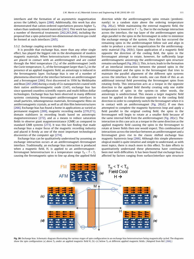
L.W. Martin et al. / Materials Science and Engineering R 68 (2010) 89–133 111
interfaces and the formation of an asymmetric magnetizationacross the LaMnO3 layers [260]. Additionally, this work has alsodemonstrated that cation-ordered superlattices possess higher TN
values than randomly mixed materials [261]. This work has spawna number of theoretical treatments [262,263,264], including theproposal that a spin-polarized two-dimensional electron gas couldbe formed at such interfaces [265].
5.5.2. Exchange coupling across interfaces
It is possible that exchange bias, more than any other singleeffect, has played the biggest role in the development of modernmagnetic materials. When heterostructures with a ferromagnetare placed in contact with an antiferromagnet and are cooledthrough the Neel temperature (TN) of the antiferromagnet (withthe Curie temperature, TC, of the ferromagnet larger than TN) in thepresence of an applied magnetic field, an anisotropy is induced inthe ferromagnetic layer. Exchange bias is one of a number ofphenomena observed at the interface between an antiferromagnetand a ferromagnet [266]. First discovered in 1956 by Meiklejohnand Bean [267,268] during a study of Co-nanoparticles coated withtheir native antiferromagnetic oxide (CoO), exchange bias hassince spawned countless scientific reports and multi-billion dollartechnologies. Exchange bias has been observed in many differentsystems containing ferromagnet–antiferromagnet interfaces insmall particles, inhomogeneous materials, ferromagnetic films onantiferromagnetic crystals, as well as all thin film heterostructures[266]. Exchange bias has found a home in applications as varied aspermanent magnets [269], magnetic recording media [270,271],domain stabilizers in recording heads based on anisotropicmagnetoresistance [272], and as a means to reduce saturationfields to observe giant magnetoresistance (GMR) as compared tostandard GMR systems [273]. It was this last finding that madeexchange bias a major focus of the magnetic recording industryand placed it firmly as one of the most important technologicaldiscoveries of the computer age [274].
Exchange bias can be qualitatively understood by assuming anexchange interaction occurs at an antiferromagnet–ferromagnetinterface. Traditionally, an exchange bias interaction is producedwhen a magnetic field, H, is applied to an antiferromagnet–ferromagnet heterostructure in a temperature range TN < T < TC
causing the ferromagnetic spins to line up along the applied field
Fig. 20. Exchange bias. Schematic diagram illustrating the various stages of spin configur
show the spin configuration (a) above TN under an applied magnetic field H, (b)–(e) be
direction while the antiferromagnetic spins remain (predomi-nantly) in a random state above the ordering temperature(Fig. 20(a)). While maintaining the external magnetic field, thetemperature is lowered to T < TN. Due to the exchange interactionacross the interface, the top layer of the antiferromagnet spinsalign parallel to the spins in the ferromagnet in order to minimizethe exchange energy of the system. Once this has occurred theremaining spins in the antiferromagnet follow suit and align inorder to produce a zero net magnetization for the antiferromag-netic material (Fig. 20(b)). Upon application of a magnetic fieldopposite the direction of the cooling field, the spins in theferromagnet attempt to rotate, however, for sufficiently largeantiferromagnetic anisotropy the antiferromagnet spin structureremains unchanged (Fig. 20(c)). This, in turn, leads to the formationof an interfacial interaction between the pinned spins in theantiferromagnet and the spins in the ferromagnet that tries tomaintain the parallel alignment of the different spin systemsacross the interface. In other words, one can think of this as anadditional internal field preventing the ferromagnet spins fromrotating freely. This interaction acts as a torque in the oppositedirection to the applied field thereby creating only one stableconfiguration of spins in the system—in other words, theanisotropy is unidirectional. This means a larger magnetic fieldmust be applied in the direction opposite to the cooling fielddirection in order to completely switch the ferromagnet when it isin contact with an antiferromagnet (Fig. 20(d)). If one thenattempted to complete the magnetic hysteresis loop and apply afield parallel to the original cooling field, the spins in theferromagnet will begin to rotate at a smaller field because ofthe same internal field from the antiferromagnet (Fig. 20(e)). Theinteraction in this case acts as a torque in the same direction as theapplied magnetic field causing the spins in the ferromagnet torotate at lower fields then one would expect. This combination ofinteractions across the interface between an antiferromagnet and aferromagnet gives rise to the classic shifted exchange biasmagnetic hysteresis loop [266]. Although this simple phenomen-ological model is quite intuitive and simple to understand, as withmost topics, there is much more to this effect. To date efforts toquantitatively understand these phenomena have continuallybeen met with difficulties. It has been found that exchange bias isaffected by factors ranging from surface/interface spin structure
ation in an exchange bias heterostructure being magnetically cycled. The diagrams
low TN at different applied magnetic fields. (Adapted from Ref. [266].)
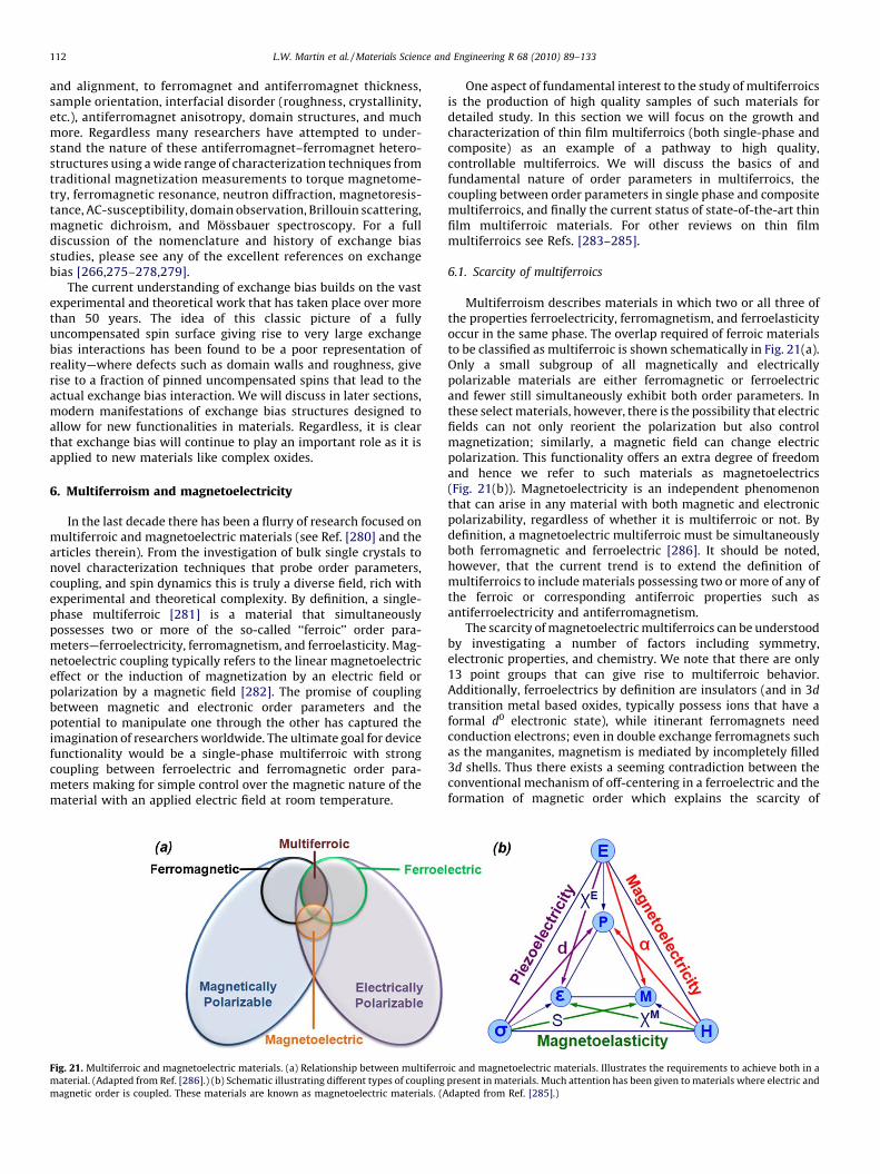
L.W. Martin et al. / Materials Science and Engineering R 68 (2010) 89–133112
and alignment, to ferromagnet and antiferromagnet thickness,sample orientation, interfacial disorder (roughness, crystallinity,etc.), antiferromagnet anisotropy, domain structures, and muchmore. Regardless many researchers have attempted to under-stand the nature of these antiferromagnet–ferromagnet hetero-structures using a wide range of characterization techniques fromtraditional magnetization measurements to torque magnetome-try, ferromagnetic resonance, neutron diffraction, magnetoresis-tance, AC-susceptibility, domain observation, Brillouin scattering,magnetic dichroism, and Mossbauer spectroscopy. For a fulldiscussion of the nomenclature and history of exchange biasstudies, please see any of the excellent references on exchangebias [266,275–278,279].
The current understanding of exchange bias builds on the vastexperimental and theoretical work that has taken place over morethan 50 years. The idea of this classic picture of a fullyuncompensated spin surface giving rise to very large exchangebias interactions has been found to be a poor representation ofreality—where defects such as domain walls and roughness, giverise to a fraction of pinned uncompensated spins that lead to theactual exchange bias interaction. We will discuss in later sections,modern manifestations of exchange bias structures designed toallow for new functionalities in materials. Regardless, it is clearthat exchange bias will continue to play an important role as it isapplied to new materials like complex oxides.
6. Multiferroism and magnetoelectricity
In the last decade there has been a flurry of research focused onmultiferroic and magnetoelectric materials (see Ref. [280] and thearticles therein). From the investigation of bulk single crystals tonovel characterization techniques that probe order parameters,coupling, and spin dynamics this is truly a diverse field, rich withexperimental and theoretical complexity. By definition, a single-phase multiferroic [281] is a material that simultaneouslypossesses two or more of the so-called ‘‘ferroic’’ order para-meters—ferroelectricity, ferromagnetism, and ferroelasticity. Mag-netoelectric coupling typically refers to the linear magnetoelectriceffect or the induction of magnetization by an electric field orpolarization by a magnetic field [282]. The promise of couplingbetween magnetic and electronic order parameters and thepotential to manipulate one through the other has captured theimagination of researchers worldwide. The ultimate goal for devicefunctionality would be a single-phase multiferroic with strongcoupling between ferroelectric and ferromagnetic order para-meters making for simple control over the magnetic nature of thematerial with an applied electric field at room temperature.
Fig. 21. Multiferroic and magnetoelectric materials. (a) Relationship between multiferro
material. (Adapted from Ref. [286].) (b) Schematic illustrating different types of coupling
magnetic order is coupled. These materials are known as magnetoelectric materials. (A
One aspect of fundamental interest to the study of multiferroicsis the production of high quality samples of such materials fordetailed study. In this section we will focus on the growth andcharacterization of thin film multiferroics (both single-phase andcomposite) as an example of a pathway to high quality,controllable multiferroics. We will discuss the basics of andfundamental nature of order parameters in multiferroics, thecoupling between order parameters in single phase and compositemultiferroics, and finally the current status of state-of-the-art thinfilm multiferroic materials. For other reviews on thin filmmultiferroics see Refs. [283–285].
6.1. Scarcity of multiferroics
Multiferroism describes materials in which two or all three ofthe properties ferroelectricity, ferromagnetism, and ferroelasticityoccur in the same phase. The overlap required of ferroic materialsto be classified as multiferroic is shown schematically in Fig. 21(a).Only a small subgroup of all magnetically and electricallypolarizable materials are either ferromagnetic or ferroelectricand fewer still simultaneously exhibit both order parameters. Inthese select materials, however, there is the possibility that electricfields can not only reorient the polarization but also controlmagnetization; similarly, a magnetic field can change electricpolarization. This functionality offers an extra degree of freedomand hence we refer to such materials as magnetoelectrics(Fig. 21(b)). Magnetoelectricity is an independent phenomenonthat can arise in any material with both magnetic and electronicpolarizability, regardless of whether it is multiferroic or not. Bydefinition, a magnetoelectric multiferroic must be simultaneouslyboth ferromagnetic and ferroelectric [286]. It should be noted,however, that the current trend is to extend the definition ofmultiferroics to include materials possessing two or more of any ofthe ferroic or corresponding antiferroic properties such asantiferroelectricity and antiferromagnetism.
The scarcity of magnetoelectric multiferroics can be understoodby investigating a number of factors including symmetry,electronic properties, and chemistry. We note that there are only13 point groups that can give rise to multiferroic behavior.Additionally, ferroelectrics by definition are insulators (and in 3d
transition metal based oxides, typically possess ions that have aformal d0 electronic state), while itinerant ferromagnets needconduction electrons; even in double exchange ferromagnets suchas the manganites, magnetism is mediated by incompletely filled3d shells. Thus there exists a seeming contradiction between theconventional mechanism of off-centering in a ferroelectric and theformation of magnetic order which explains the scarcity of
ic and magnetoelectric materials. Illustrates the requirements to achieve both in a
present in materials. Much attention has been given to materials where electric and
dapted from Ref. [285].)
L.W. Martin et al. / Materials Science and Engineering R 68 (2010) 89–133 113
ferromagnetic–ferroelectric multiferroics [62]. The focus of manyresearchers, therefore, has been in designing and identifying newmechanisms that lead to magnetoelectric coupling and multi-ferroic behavior. In the following section we will investigate anumber of these pathways.
6.2. Pathways to multiferroism
There are a number of pathways with which one can achievemultiferroism in materials that can be broken down into one of twotypes as elegantly described by Khomskii [287]. Type I multi-ferroics are materials in which ferroelectricity and magnetismhave different sources and appear largely independent of oneanother. One can create a Type I multiferroic by engineering thefunctionality on a site-by-site basis in model systems like theperovskites (ABO3) where one can make use of the stereochemicalactivity of an A-site cation with a lone pair (i.e., 6s electrons in Bi orPb) to induce a structural distortion and ferroelectricity whileinducing magnetism with the B-site cation. This is the case in oneof the most widely studied single phase multiferroics—theantiferromagnetic, ferroelectric BiFeO3 [288]. Another way toachieve such Type I multiferroics is through geometrically driveneffects where long-range dipole–dipole interactions and anionrotations drive the system towards a stable ferroelectric state. Thisis thought to drive multiferroism in materials like YMnO3 [289].Finally there can also be charge ordering driven multiferroicswhere non-centrosymmetric charge ordering arrangements resultin ferroelectricity in magnetic materials as is found in LuFe2O4
[290]. On the other hand, Type II multiferroics are materials inwhich magnetism causes ferroelectricity—implying a strongcoupling between the two order parameters. The prototypicalexamples of this sort of behavior are TbMnO3 [291] and TbMn2O5
[292] where ferroelectricity is induced by the formation of asymmetry-lowering magnetic ground state that lacks inversionsymmetry.
6.3. Definition of magnetoelectricity
From an applications standpoint, the real interest in multi-ferroic materials lies in the possibility of strong magnetoelectriccoupling and the possibility to create new functionalities inmaterials. The magnetoelectric effect was proposed as early as1894 by Curie [293], but experimental confirmation of the effectremained elusive until work on Cr2O3 in the 1960s [294,295]. Asearly as the 1970s a wide range of devices, including devices for themodulation of amplitudes, polarizations, and phases of opticalwaves, magnetoelectric data storage and switching, optical diodes,spin-wave generation, amplification, and frequency conversionhad been proposed that would take advantage of magnetoelectricmaterials [296]. The magnetoelectric effect in its most generaldefinition delineates the coupling between electric and magneticfields in matter. A better understanding of magnetoelectriccoupling arises from expansion of the free energy of a material, i.e.
Fð~E; ~HÞ ¼ F0 � PSi Ei �MS
i Hi �1
2e0ei jEiE j �
1
2m0mi jHiH j
� 1
2bi jkEiH jHk �
1
2g i jkHiE jEk � � � � (6)
with ~E and ~H as the electric field and magnetic field, respectively.Differentiation leads to the constitutive order parameters polar-ization
Pi ¼ ð~E; ~HÞ ¼ �@F
@Ei
¼ PSi þ e0ei jE j þ ai jH j þ
1
2bi jkH jHk þ g i jkHiE j þ � � � (7)
and magnetization
Mi ¼ ð~E; ~HÞ ¼ �@F
@Hi
¼ MSi þm0mi jH j þ ai jE j þ bi jkEiH j þ
1
2g i jkE jEk þ � � � (8)
where e and m are the electric and magnetic susceptibilitiesrespectively and a represents the induction of polarization by amagnetic field or magnetization by electric field and is designatedthe linear magnetoelectric effect. It should be noted that higherorder magnetoelectric effects like b and g are possible, however,they are often much smaller in magnitude then the lower orderterms. Furthermore, it can be shown that the magnetoelectricresponse is limited by the relation a2
i j < eiim j j or more rigorouslya2
i j <xeiix
mj j where xe and xm are the electric and magnetic
susceptibilities. This means that the magnetoelectric effect canonly be large in ferroelectric and/or ferromagnetic materials. Todate the largest magnetoelectric responses have been identified incomposite materials where the magnetoelectric effect is theproduct property of a magnetostrictive and a piezoelectric materialand in multiferroic materials [297].
6.4. Thin film multiferroics
The re-emergence of interest in multiferroics has been driven, inpart, by the development of thin film growth techniques that allowfor the production of non-equilibrium phases of materials and strainengineering of existing materials [9]. Thin films offer a pathway tothe discovery and stabilization of a number of new multiferroics inconjunction with the availability of high quality materials that canbe produced in larger lateral sizes than single crystal samples.Multiferroic thin films and nanostructures have been producedusing a wide variety of growth techniques including sputtering, spincoating, pulsed laser deposition, sol–gel processes, metal-organicchemical vapor deposition, molecular beam epitaxy, and more.
Despite the fact that there are a number of algorithms withwhich one can create multiferroism in materials, to date the onlysingle-phase multiferroics produced as thin films include thehexagonal manganites and Bi- and Pb-based perovskites. In thissection we will investigate these single-phase thin film multi-ferroics in more detail.
6.4.1. Manganite multiferroic thin films
The rare-earth manganites (REMnO3) are an intriguing materi-als system and depending on the size of the RE ion the structuretakes on an equilibrium orthorhombic (RE = La–Dy) or hexagonal(RE = Ho–Lu, as well as Y) structure [298]. All of the hexagonal rare-earth manganites are known to show multiferroic behavior withrelatively high ferroelectric ordering temperatures (typically inexcess of 590 K) and relatively low magnetic ordering tempera-tures (typically between 70 and 120 K) [299]. In these hexagonalphases, the ferroelectric ordering is related to the tilting of the rigidMnO5 trigonal bipyramid [289]. On the other hand, only theorthorhombic phases with RE = Dy, Tb, and Gd are multiferroic innature and have very low (�20–30 K) ferroelectric orderingtemperatures [300,301]. In these materials the ferroelectricityarises from magnetic ordering induced lattice modulations.
One of the earliest thin film multiferroic manganites to beproduced was the hexagonal manganite YMnO3 (YMO) (Fig. 22(a))[302]. Work on YMO in the 1960s suggested that it was both aferroelectric [303] and an A-type antiferromagnet [304]; however,it was not until sometime later that the true nature offerroelectricity in this material was understood to arise from longrange dipole–dipole interactions and oxygen rotations workingtogether to drive the system towards a stable ferroelectric state
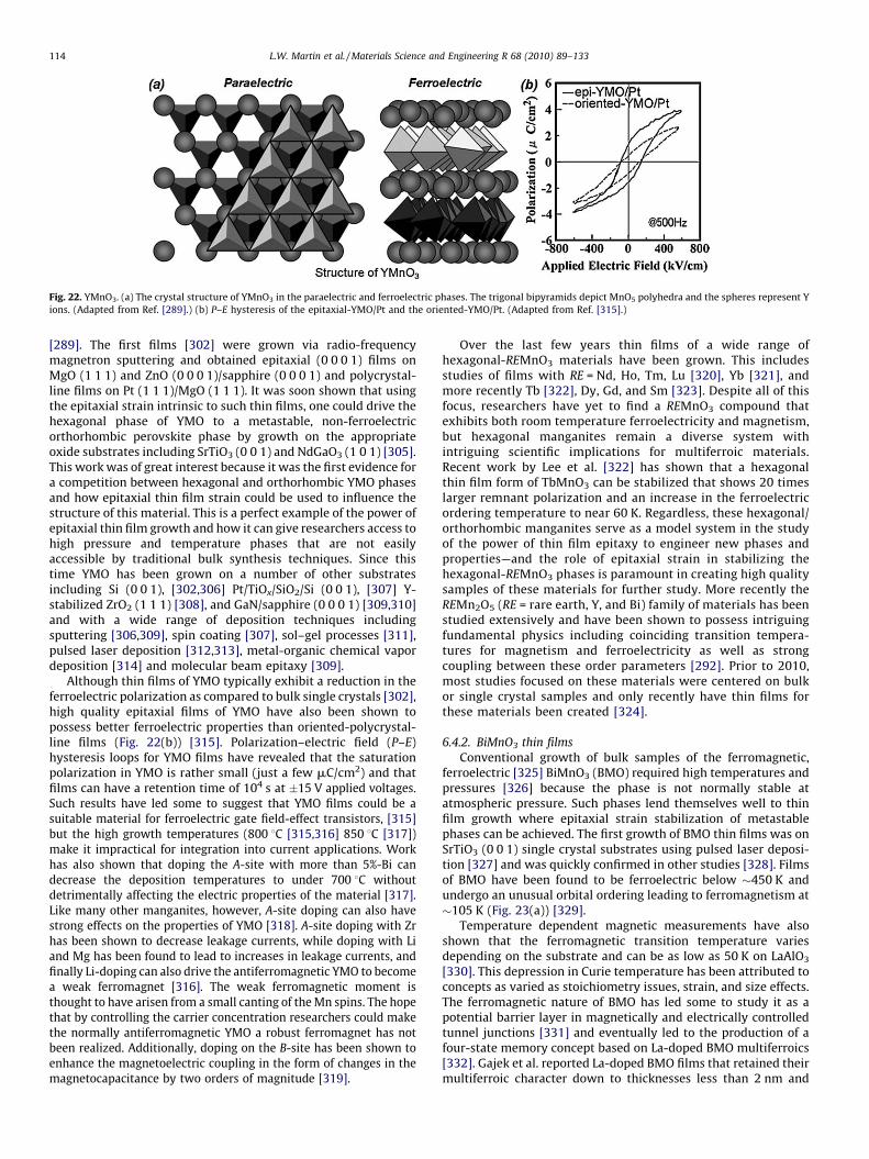
Fig. 22. YMnO3. (a) The crystal structure of YMnO3 in the paraelectric and ferroelectric phases. The trigonal bipyramids depict MnO5 polyhedra and the spheres represent Y
ions. (Adapted from Ref. [289].) (b) P–E hysteresis of the epitaxial-YMO/Pt and the oriented-YMO/Pt. (Adapted from Ref. [315].)
L.W. Martin et al. / Materials Science and Engineering R 68 (2010) 89–133114
[289]. The first films [302] were grown via radio-frequencymagnetron sputtering and obtained epitaxial (0 0 0 1) films onMgO (1 1 1) and ZnO (0 0 0 1)/sapphire (0 0 0 1) and polycrystal-line films on Pt (1 1 1)/MgO (1 1 1). It was soon shown that usingthe epitaxial strain intrinsic to such thin films, one could drive thehexagonal phase of YMO to a metastable, non-ferroelectricorthorhombic perovskite phase by growth on the appropriateoxide substrates including SrTiO3 (0 0 1) and NdGaO3 (1 0 1) [305].This work was of great interest because it was the first evidence fora competition between hexagonal and orthorhombic YMO phasesand how epitaxial thin film strain could be used to influence thestructure of this material. This is a perfect example of the power ofepitaxial thin film growth and how it can give researchers access tohigh pressure and temperature phases that are not easilyaccessible by traditional bulk synthesis techniques. Since thistime YMO has been grown on a number of other substratesincluding Si (0 0 1), [302,306] Pt/TiOx/SiO2/Si (0 0 1), [307] Y-stabilized ZrO2 (1 1 1) [308], and GaN/sapphire (0 0 0 1) [309,310]and with a wide range of deposition techniques includingsputtering [306,309], spin coating [307], sol–gel processes [311],pulsed laser deposition [312,313], metal-organic chemical vapordeposition [314] and molecular beam epitaxy [309].
Although thin films of YMO typically exhibit a reduction in theferroelectric polarization as compared to bulk single crystals [302],high quality epitaxial films of YMO have also been shown topossess better ferroelectric properties than oriented-polycrystal-line films (Fig. 22(b)) [315]. Polarization–electric field (P–E)hysteresis loops for YMO films have revealed that the saturationpolarization in YMO is rather small (just a few mC/cm2) and thatfilms can have a retention time of 104 s at �15 V applied voltages.Such results have led some to suggest that YMO films could be asuitable material for ferroelectric gate field-effect transistors, [315]but the high growth temperatures (800 8C [315,316] 850 8C [317])make it impractical for integration into current applications. Workhas also shown that doping the A-site with more than 5%-Bi candecrease the deposition temperatures to under 700 8C withoutdetrimentally affecting the electric properties of the material [317].Like many other manganites, however, A-site doping can also havestrong effects on the properties of YMO [318]. A-site doping with Zrhas been shown to decrease leakage currents, while doping with Liand Mg has been found to lead to increases in leakage currents, andfinally Li-doping can also drive the antiferromagnetic YMO to becomea weak ferromagnet [316]. The weak ferromagnetic moment isthought to have arisen from a small canting of the Mn spins. The hopethat by controlling the carrier concentration researchers could makethe normally antiferromagnetic YMO a robust ferromagnet has notbeen realized. Additionally, doping on the B-site has been shown toenhance the magnetoelectric coupling in the form of changes in themagnetocapacitance by two orders of magnitude [319].
Over the last few years thin films of a wide range ofhexagonal-REMnO3 materials have been grown. This includesstudies of films with RE = Nd, Ho, Tm, Lu [320], Yb [321], andmore recently Tb [322], Dy, Gd, and Sm [323]. Despite all of thisfocus, researchers have yet to find a REMnO3 compound thatexhibits both room temperature ferroelectricity and magnetism,but hexagonal manganites remain a diverse system withintriguing scientific implications for multiferroic materials.Recent work by Lee et al. [322] has shown that a hexagonalthin film form of TbMnO3 can be stabilized that shows 20 timeslarger remnant polarization and an increase in the ferroelectricordering temperature to near 60 K. Regardless, these hexagonal/orthorhombic manganites serve as a model system in the studyof the power of thin film epitaxy to engineer new phases andproperties—and the role of epitaxial strain in stabilizing thehexagonal-REMnO3 phases is paramount in creating high qualitysamples of these materials for further study. More recently theREMn2O5 (RE = rare earth, Y, and Bi) family of materials has beenstudied extensively and have been shown to possess intriguingfundamental physics including coinciding transition tempera-tures for magnetism and ferroelectricity as well as strongcoupling between these order parameters [292]. Prior to 2010,most studies focused on these materials were centered on bulkor single crystal samples and only recently have thin films forthese materials been created [324].
6.4.2. BiMnO3 thin films
Conventional growth of bulk samples of the ferromagnetic,ferroelectric [325] BiMnO3 (BMO) required high temperatures andpressures [326] because the phase is not normally stable atatmospheric pressure. Such phases lend themselves well to thinfilm growth where epitaxial strain stabilization of metastablephases can be achieved. The first growth of BMO thin films was onSrTiO3 (0 0 1) single crystal substrates using pulsed laser deposi-tion [327] and was quickly confirmed in other studies [328]. Filmsof BMO have been found to be ferroelectric below �450 K andundergo an unusual orbital ordering leading to ferromagnetism at�105 K (Fig. 23(a)) [329].
Temperature dependent magnetic measurements have alsoshown that the ferromagnetic transition temperature variesdepending on the substrate and can be as low as 50 K on LaAlO3
[330]. This depression in Curie temperature has been attributed toconcepts as varied as stoichiometry issues, strain, and size effects.The ferromagnetic nature of BMO has led some to study it as apotential barrier layer in magnetically and electrically controlledtunnel junctions [331] and eventually led to the production of afour-state memory concept based on La-doped BMO multiferroics[332]. Gajek et al. reported La-doped BMO films that retained theirmultiferroic character down to thicknesses less than 2 nm and
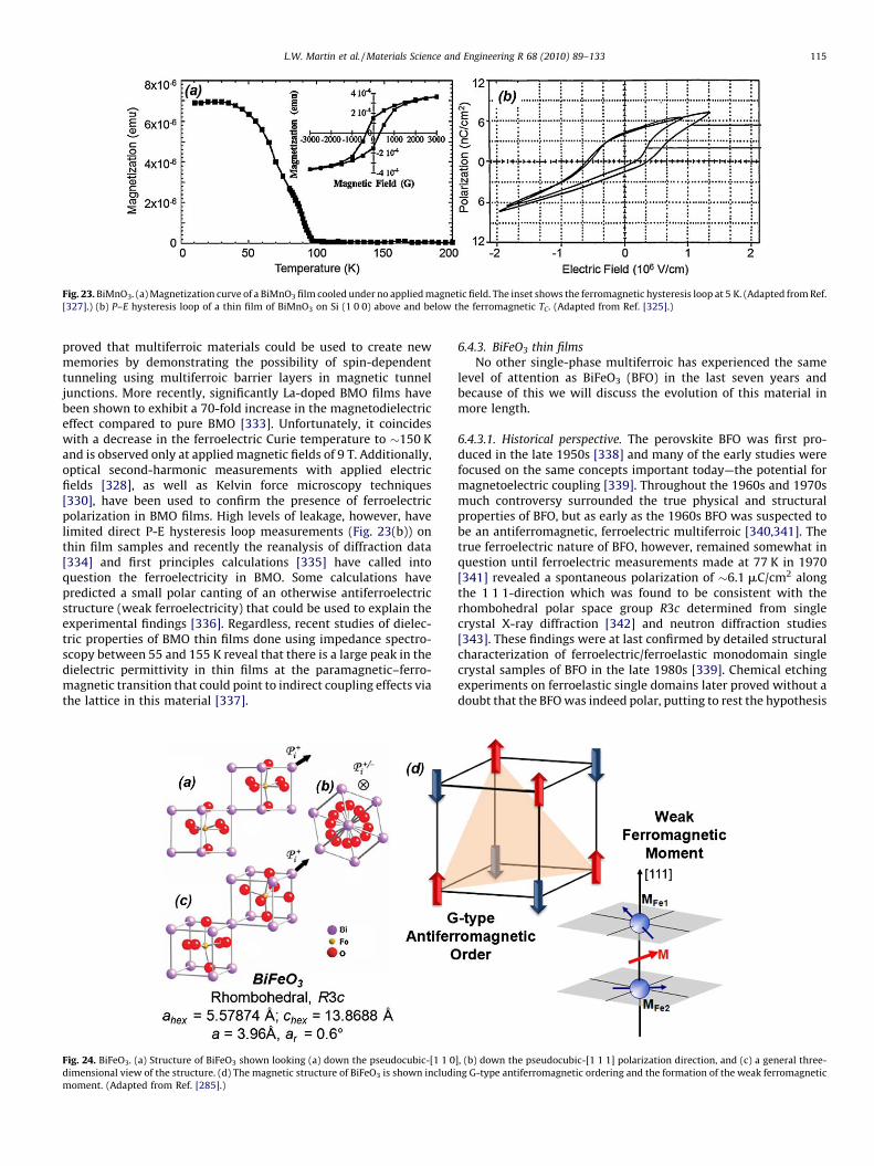
Fig. 23. BiMnO3. (a) Magnetization curve of a BiMnO3 film cooled under no applied magnetic field. The inset shows the ferromagnetic hysteresis loop at 5 K. (Adapted from Ref.
[327].) (b) P–E hysteresis loop of a thin film of BiMnO3 on Si (1 0 0) above and below the ferromagnetic TC. (Adapted from Ref. [325].)
L.W. Martin et al. / Materials Science and Engineering R 68 (2010) 89–133 115
proved that multiferroic materials could be used to create newmemories by demonstrating the possibility of spin-dependenttunneling using multiferroic barrier layers in magnetic tunneljunctions. More recently, significantly La-doped BMO films havebeen shown to exhibit a 70-fold increase in the magnetodielectriceffect compared to pure BMO [333]. Unfortunately, it coincideswith a decrease in the ferroelectric Curie temperature to �150 Kand is observed only at applied magnetic fields of 9 T. Additionally,optical second-harmonic measurements with applied electricfields [328], as well as Kelvin force microscopy techniques[330], have been used to confirm the presence of ferroelectricpolarization in BMO films. High levels of leakage, however, havelimited direct P-E hysteresis loop measurements (Fig. 23(b)) onthin film samples and recently the reanalysis of diffraction data[334] and first principles calculations [335] have called intoquestion the ferroelectricity in BMO. Some calculations havepredicted a small polar canting of an otherwise antiferroelectricstructure (weak ferroelectricity) that could be used to explain theexperimental findings [336]. Regardless, recent studies of dielec-tric properties of BMO thin films done using impedance spectro-scopy between 55 and 155 K reveal that there is a large peak in thedielectric permittivity in thin films at the paramagnetic–ferro-magnetic transition that could point to indirect coupling effects viathe lattice in this material [337].
Fig. 24. BiFeO3. (a) Structure of BiFeO3 shown looking (a) down the pseudocubic-[1 1 0
dimensional view of the structure. (d) The magnetic structure of BiFeO3 is shown includi
moment. (Adapted from Ref. [285].)
6.4.3. BiFeO3 thin films
No other single-phase multiferroic has experienced the samelevel of attention as BiFeO3 (BFO) in the last seven years andbecause of this we will discuss the evolution of this material inmore length.
6.4.3.1. Historical perspective. The perovskite BFO was first pro-duced in the late 1950s [338] and many of the early studies werefocused on the same concepts important today—the potential formagnetoelectric coupling [339]. Throughout the 1960s and 1970smuch controversy surrounded the true physical and structuralproperties of BFO, but as early as the 1960s BFO was suspected tobe an antiferromagnetic, ferroelectric multiferroic [340,341]. Thetrue ferroelectric nature of BFO, however, remained somewhat inquestion until ferroelectric measurements made at 77 K in 1970[341] revealed a spontaneous polarization of �6.1 mC/cm2 alongthe 1 1 1-direction which was found to be consistent with therhombohedral polar space group R3c determined from singlecrystal X-ray diffraction [342] and neutron diffraction studies[343]. These findings were at last confirmed by detailed structuralcharacterization of ferroelectric/ferroelastic monodomain singlecrystal samples of BFO in the late 1980s [339]. Chemical etchingexperiments on ferroelastic single domains later proved without adoubt that the BFO was indeed polar, putting to rest the hypothesis
], (b) down the pseudocubic-[1 1 1] polarization direction, and (c) a general three-
ng G-type antiferromagnetic ordering and the formation of the weak ferromagnetic
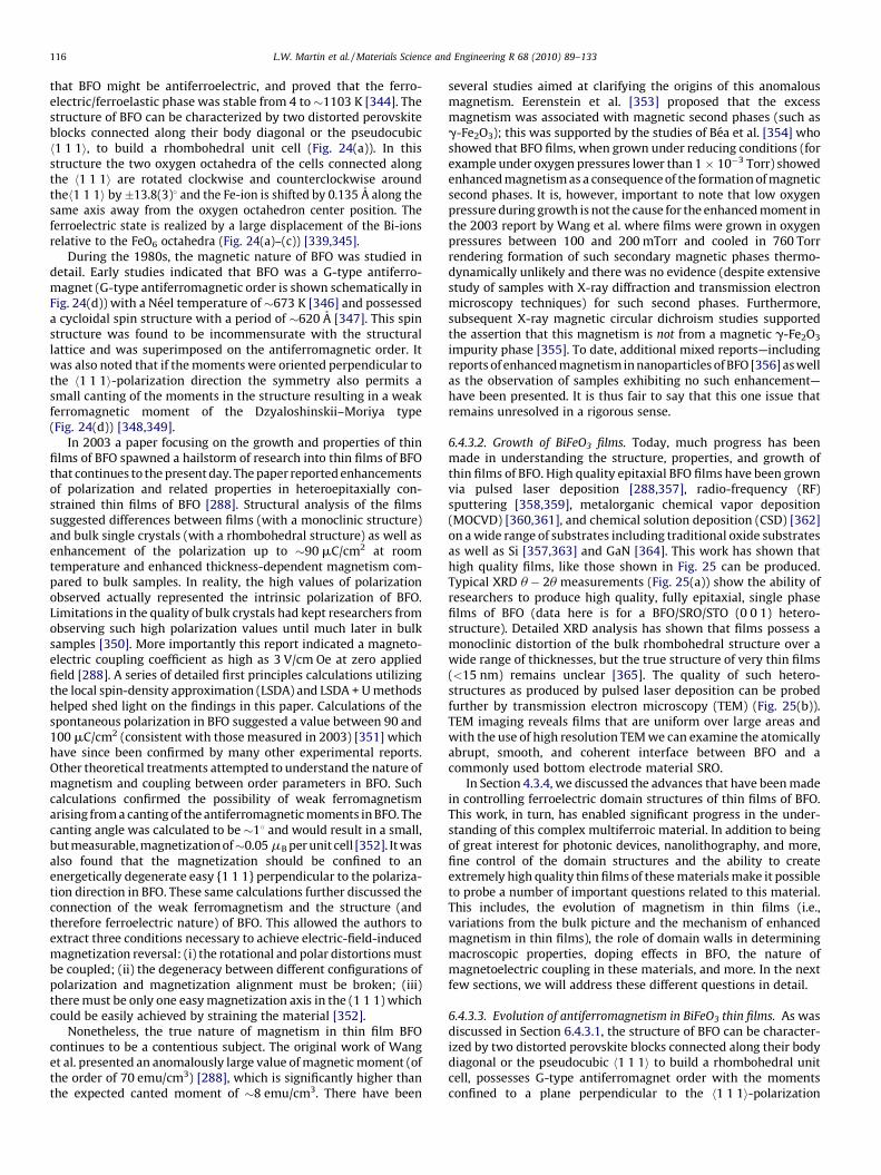
L.W. Martin et al. / Materials Science and Engineering R 68 (2010) 89–133116
that BFO might be antiferroelectric, and proved that the ferro-electric/ferroelastic phase was stable from 4 to�1103 K [344]. Thestructure of BFO can be characterized by two distorted perovskiteblocks connected along their body diagonal or the pseudocubich1 1 1i, to build a rhombohedral unit cell (Fig. 24(a)). In thisstructure the two oxygen octahedra of the cells connected alongthe h1 1 1i are rotated clockwise and counterclockwise aroundtheh1 1 1i by �13.8(3)8 and the Fe-ion is shifted by 0.135 A along thesame axis away from the oxygen octahedron center position. Theferroelectric state is realized by a large displacement of the Bi-ionsrelative to the FeO6 octahedra (Fig. 24(a)–(c)) [339,345].
During the 1980s, the magnetic nature of BFO was studied indetail. Early studies indicated that BFO was a G-type antiferro-magnet (G-type antiferromagnetic order is shown schematically inFig. 24(d)) with a Neel temperature of�673 K [346] and possesseda cycloidal spin structure with a period of �620 A [347]. This spinstructure was found to be incommensurate with the structurallattice and was superimposed on the antiferromagnetic order. Itwas also noted that if the moments were oriented perpendicular tothe h1 1 1i-polarization direction the symmetry also permits asmall canting of the moments in the structure resulting in a weakferromagnetic moment of the Dzyaloshinskii–Moriya type(Fig. 24(d)) [348,349].
In 2003 a paper focusing on the growth and properties of thinfilms of BFO spawned a hailstorm of research into thin films of BFOthat continues to the present day. The paper reported enhancementsof polarization and related properties in heteroepitaxially con-strained thin films of BFO [288]. Structural analysis of the filmssuggested differences between films (with a monoclinic structure)and bulk single crystals (with a rhombohedral structure) as well asenhancement of the polarization up to �90 mC/cm2 at roomtemperature and enhanced thickness-dependent magnetism com-pared to bulk samples. In reality, the high values of polarizationobserved actually represented the intrinsic polarization of BFO.Limitations in the quality of bulk crystals had kept researchers fromobserving such high polarization values until much later in bulksamples [350]. More importantly this report indicated a magneto-electric coupling coefficient as high as 3 V/cm Oe at zero appliedfield [288]. A series of detailed first principles calculations utilizingthe local spin-density approximation (LSDA) and LSDA + U methodshelped shed light on the findings in this paper. Calculations of thespontaneous polarization in BFO suggested a value between 90 and100 mC/cm2 (consistent with those measured in 2003) [351] whichhave since been confirmed by many other experimental reports.Other theoretical treatments attempted to understand the nature ofmagnetism and coupling between order parameters in BFO. Suchcalculations confirmed the possibility of weak ferromagnetismarising from a canting of the antiferromagnetic moments in BFO. Thecanting angle was calculated to be �18 and would result in a small,but measurable, magnetization of�0.05 mB per unit cell [352]. It wasalso found that the magnetization should be confined to anenergetically degenerate easy {1 1 1} perpendicular to the polariza-tion direction in BFO. These same calculations further discussed theconnection of the weak ferromagnetism and the structure (andtherefore ferroelectric nature) of BFO. This allowed the authors toextract three conditions necessary to achieve electric-field-inducedmagnetization reversal: (i) the rotational and polar distortions mustbe coupled; (ii) the degeneracy between different configurations ofpolarization and magnetization alignment must be broken; (iii)there must be only one easy magnetization axis in the (1 1 1) whichcould be easily achieved by straining the material [352].
Nonetheless, the true nature of magnetism in thin film BFOcontinues to be a contentious subject. The original work of Wanget al. presented an anomalously large value of magnetic moment (ofthe order of 70 emu/cm3) [288], which is significantly higher thanthe expected canted moment of �8 emu/cm3. There have been
several studies aimed at clarifying the origins of this anomalousmagnetism. Eerenstein et al. [353] proposed that the excessmagnetism was associated with magnetic second phases (such asg-Fe2O3); this was supported by the studies of Bea et al. [354] whoshowed that BFO films, when grown under reducing conditions (forexample under oxygen pressures lower than 1 � 10�3 Torr) showedenhanced magnetism as a consequence of the formation of magneticsecond phases. It is, however, important to note that low oxygenpressure during growth is not the cause for the enhanced moment inthe 2003 report by Wang et al. where films were grown in oxygenpressures between 100 and 200 mTorr and cooled in 760 Torrrendering formation of such secondary magnetic phases thermo-dynamically unlikely and there was no evidence (despite extensivestudy of samples with X-ray diffraction and transmission electronmicroscopy techniques) for such second phases. Furthermore,subsequent X-ray magnetic circular dichroism studies supportedthe assertion that this magnetism is not from a magnetic g-Fe2O3
impurity phase [355]. To date, additional mixed reports—includingreports of enhanced magnetism in nanoparticles of BFO [356] as wellas the observation of samples exhibiting no such enhancement—have been presented. It is thus fair to say that this one issue thatremains unresolved in a rigorous sense.
6.4.3.2. Growth of BiFeO3 films. Today, much progress has beenmade in understanding the structure, properties, and growth ofthin films of BFO. High quality epitaxial BFO films have been grownvia pulsed laser deposition [288,357], radio-frequency (RF)sputtering [358,359], metalorganic chemical vapor deposition(MOCVD) [360,361], and chemical solution deposition (CSD) [362]on a wide range of substrates including traditional oxide substratesas well as Si [357,363] and GaN [364]. This work has shown thathigh quality films, like those shown in Fig. 25 can be produced.Typical XRD u � 2u measurements (Fig. 25(a)) show the ability ofresearchers to produce high quality, fully epitaxial, single phasefilms of BFO (data here is for a BFO/SRO/STO (0 0 1) hetero-structure). Detailed XRD analysis has shown that films possess amonoclinic distortion of the bulk rhombohedral structure over awide range of thicknesses, but the true structure of very thin films(<15 nm) remains unclear [365]. The quality of such hetero-structures as produced by pulsed laser deposition can be probedfurther by transmission electron microscopy (TEM) (Fig. 25(b)).TEM imaging reveals films that are uniform over large areas andwith the use of high resolution TEM we can examine the atomicallyabrupt, smooth, and coherent interface between BFO and acommonly used bottom electrode material SRO.
In Section 4.3.4, we discussed the advances that have been madein controlling ferroelectric domain structures of thin films of BFO.This work, in turn, has enabled significant progress in the under-standing of this complex multiferroic material. In addition to beingof great interest for photonic devices, nanolithography, and more,fine control of the domain structures and the ability to createextremely high quality thin films of these materials make it possibleto probe a number of important questions related to this material.This includes, the evolution of magnetism in thin films (i.e.,variations from the bulk picture and the mechanism of enhancedmagnetism in thin films), the role of domain walls in determiningmacroscopic properties, doping effects in BFO, the nature ofmagnetoelectric coupling in these materials, and more. In the nextfew sections, we will address these different questions in detail.
6.4.3.3. Evolution of antiferromagnetism in BiFeO3 thin films. As wasdiscussed in Section 6.4.3.1, the structure of BFO can be character-ized by two distorted perovskite blocks connected along their bodydiagonal or the pseudocubic h1 1 1i to build a rhombohedral unitcell, possesses G-type antiferromagnet order with the momentsconfined to a plane perpendicular to the h1 1 1i-polarization
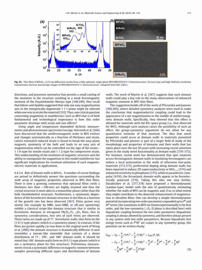
Fig. 25. . Thin films of BiFeO3. (a) X-ray diffraction results from a fully epitaxial, single phase BFO/SRO/STO(0 0 1) heterostructure. (b) Low (top) and high (bottom) resolution
transmission electron microscopy images of BFO/SRO/STO(0 0 1) heterostructure. (Adapted from Ref. [285].)
L.W. Martin et al. / Materials Science and Engineering R 68 (2010) 89–133 117
directions, and possesses symmetry that permits a small canting ofthe moments in the structure resulting in a weak ferromagneticmoment of the Dzyaloshinskii–Moriya type [348,349]. Also recallthat Ederer and Spaldin suggested that only one easy magnetizationaxis in the energetically degenerate 1 1 1-plane might be selectedwhen one was to strain the material [352]. Thus, one critical questionconcerning magnetism in multiferroics such as BFO that is of bothfundamental and technological importance is how this orderparameter develops with strain and size effects?
Using angle and temperature dependent dichroic measure-ments and photoemission spectromicroscopy, Holcomb et al. [366]have discovered that the antiferromagnetic order in BFO evolvesand changes systematically as a function of thickness and strain.Lattice mismatch induced strain is found to break the easy-planemagnetic symmetry of the bulk and leads to an easy axis ofmagnetization which can be controlled via the sign of the strain—1 1 0-type for tensile strain and 1 1 2-type for compressive strain.This understanding of the evolution of magnetic structure and theability to manipulate the magnetism in this model multiferroic hassignificant implications for eventual utilization of such magneto-electric materials in applications.
6.4.3.4. Role of domain walls in BiFeO3. A number of recent findingsare poised to definitively answer the questions surrounding thewide array of magnetic properties observed in BFO thin films.There is now a growing consensus that epitaxial films (with athickness less than �100 nm) are highly strained and thus thecrystal structure is more akin to a monoclinic phase rather than thebulk rhombohedral structure. Furthermore, a systematic depen-dence of the ferroelectric domain structure in the film as a functionof the growth rate has been observed [367]. Films grown veryslowly (for example by MBE, laser-MBE, or off-axis sputtering)exhibit a classical stripe-like domain structure that is similar toferroelastic domains in tetragonal Pb(Zrx,Ti1�x)O3 films. Due tosymmetry considerations, two sets of such twins are observed.These twins are made up of 718 ferroelastic walls, that form on the{1 0 1}-type planes (which is a symmetry plane). In contrast, if thefilms are grown rapidly (as was done in the original work of Wanget al. [288]) the domain structure is dramatically different. It nowresembles a mosaic-like ensemble that consists of a densedistribution of 718, 1098, and 1808 domain walls. It should benoted that 1098 domain walls form on {0 0 1}-type planes (which isnot a symmetry plane for this structure). Preliminary measure-ments reveal a systematic difference in magnetic moment betweensamples possessing different types and distributions of domain
walls. The work of Martin et al. [367] suggests that such domainwalls could play a key role in the many observations of enhancedmagnetic moment in BFO thin films.
This suggestion builds off of the work of Prıvratska and Janovec[368,369], where detailed symmetry analyzes were used to makethe conclusion that magnetoelectric coupling could lead to theappearance of a net magnetization in the middle of antiferromag-netic domain walls. Specifically, they showed that this effect isallowed for materials with the R3c space group (i.e., that observedfor BFO). Although such analysis raises the possibility of such aneffect, the group-symmetry arguments do not allow for anyquantitative estimate of that moment. The idea that novelproperties could occur at domain walls in materials presentedby Prıvratska and Janovec is part of a larger field of study of themorphology and properties of domains and their walls that hastaken place over the last 50 years with increasing recent attentiongiven to the study novel functionality at domain walls [370–372].For instance, recent work has demonstrated that spin rotationsacross ferromagnetic domain walls in insulating ferromagnets caninduce a local polarization in the walls of otherwise non-polarmaterials [372,373], preferential doping along domain walls hasbeen reported to induce 2D superconductivity in WO3�x [374] andenhanced resistivity in phosphates [375], while in paraelectric (non-polar) SrTiO3 the ferroelastic domain walls appear to be ferroelec-trically polarized [376]. Taking this idea one step further,Daraktchiev et al. [377,378] have proposed a thermodynamic(Landau-type) model with the aim of quantitatively estimatingwhether the walls of BFO can be magnetic and, if so, to what extentthey might contribute to the observed enhancement of magnetiza-tion in ultrathin films. One can develop a simple thermodynamicpotential incorporating two order parameters expanded up to P6 andM6 terms (the transitions in BFO are found experimentally to be firstorder, and the low-symmetry (�P0, 0) phase is described here) withbiquadratic coupling between the two order parameters (biquadraticcoupling is always allowed by symmetry, and therefore always presentin any system with two order parameters). Because biquadratic freeenergy terms such as P2M2 are scalars in any symmetry group, thispotential can be written thusly:
GMP ¼ G0 þk2rPð Þ2 þ l
2rMð Þ2 þ LMP P;Mð Þ
¼ G0 þk2rPð Þ2 þ l
2rMð Þ2 þ a
2P2 þ b
4P4 þ h
6P6 þ a
2M2
þ b
4M4 þ n
6M6 þ g
2P2M2 (9)
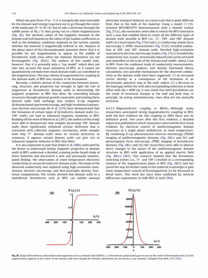
L.W. Martin et al. / Materials Science and Engineering R 68 (2010) 89–133118
When one goes from +P to�P, it is energetically more favorablefor the domain wall energy trajectory not to go through the centreof the landscape (P = 0, M = 0), but to take a diversion through thesaddle points at M0 6¼ 0, thus giving rise to a finite magnetization(Fig. 26). The absolute values of the magnetic moment at thedomain wall will depend on the values of the Landau coefficients aswell as the boundary conditions imposed on the system, namelywhether the material is magnetically ordered or not. Analysis ofthe phase space of this thermodynamic potential shows that it ispossible for net magnetization to appear in the middle offerroelectric walls even when the domains themselves are notferromagnetic (Fig. 26(b)). The authors of this model note,however, that it is presently only a ‘‘toy model’’ which does nottake into account the exact symmetry of BFO, so it cannot yetquantitatively estimate how much domain walls can contribute tothe magnetization. The exact theory of magnetoelectric coupling atthe domain walls of BFO also remains to be formulated.
Recently, a holistic picture of the connection between proces-sing, structure, and properties has brought to light the role ofmagnetism at ferroelectric domain walls in determining themagnetic properties in BFO thin films. By controlling domainstructures through epitaxial growth constraints and probing thesedomain walls with exchange bias studies, X-ray magneticdichroism based spectromicroscopy, and high resolution transmis-sion electron microscopy He et al. [379] have demonstrated thatthe formation of certain types of ferroelectric domain walls (i.e.,1098 walls) can lead to enhanced magnetic moments in BFO.Building off the work of Martin et al. [367], the authors of this studywere able to demonstrate that samples possessing 1098 domainwalls show significantly enhanced circular dichroism that isconsistent with collective magnetic correlations, while sampleswith only 718 domain walls show no circular dichroism. Insummary, it appears certain domain walls can give rise toenhanced magnetic behavior in BFO thin films.
It is also important to note that Seidel et al. [380], motivated bythe desire to understand similar magnetic properties at domainwalls in BFO, undertook a detailed scanning probe-based study ofthese materials and discovered a new and previously unantici-pated finding: the observation of room temperature electronicconductivity at certain ferroelectric domain walls. The origin of theobserved conductivity was explored using high-resolution trans-mission electron microscopy and first-principles density func-tional computations. The results showed that domain walls in amultiferroic ferroelectric such as BFO, can exhibit unusual
Fig. 26. Shape of ferroelectric polarization and magnetism across a domain wall in BiFeO3
magnetization appears at the center of the domain wall even though the domains the
electronic transport behavior on a local scale that is quite differentfrom that in the bulk of the material. Using a model (1 1 0)-oriented BFO/SRO/STO heterostructure with a smooth surface(Fig. 27(a)), the researchers were able to switch the BFO material insuch a way that enabled them to create all the different types ofdomain walls possible in BFO (i.e., 718, 1098, and 1808 domainwalls) in a local region (Fig. 27(b) and (c)). Conducting-atomic forcemicroscopy (c-AFM) measurements (Fig. 27(d)) revealed conduc-tion at 1098 and 1808 domain walls. Detailed high-resolutiontransmission electron microscopy studies (Fig. 27(e)) revealed thisconductivity was, in part, structurally induced and can be activatedand controlled on the scale of the domain wall width—about 2 nmin BFO. From the combined study of conductivity measurements,electron microscopy analysis, and density functional theorycalculations, two possible mechanisms for the observed conduc-tivity at the domain walls have been suggested: (1) an increasedcarrier density as a consequence of the formation of anelectrostatic potential step at the wall; and/or (2) a decrease inthe band gap within the wall and corresponding reduction in bandoffset with the c-AFM tip. It was noted that both possibilities arethe result of structural changes at the wall and both may, inprinciple, be acting simultaneously, since they are not mutuallyexclusive.
6.4.3.5. Magnetoelectric coupling in BiFeO3. Although manyresearchers anticipated strong magnetoelectric coupling in BFO,until the first evidence for this coupling in 2003 there was nodefinitive proof. Two years after this first evidence, a detailedreport was published in which researchers observed the first visualevidence for electrical control of antiferromagnetic domainstructures in a single phase multiferroic at room temperature.By combining X-ray photoemission electron microscopy (PEEM)imaging of antiferromagnetic domains (Fig. 28(a) and (b)) andpiezoresponse force microscopy (PFM) imaging of ferroelectricdomains (Fig. 28(c) and (d)) the researchers were able to observedirect changes in the nature of the antiferromagnetic domainstructure in BFO with application of an applied electric field(Fig. 28(e)) [381]. This research showed that the ferroelasticswitching events (i.e., 718 and 1098) resulted in a correspondingrotation of the magnetization plane in BFO (Fig. 28(f)) and haspaved the way for further study of this material in attempts to gainroom temperature control of ferromagnetism (to be discussed indetail later). This work has since been confirmed by neutrondiffraction experiments in bulk BFO as well [382].
. (a) Ferroelectric polarization goes to zero at the center of the domain wall. (b) A net
mselves do not possess a net moment. (Adapted from Refs. [377,378].)
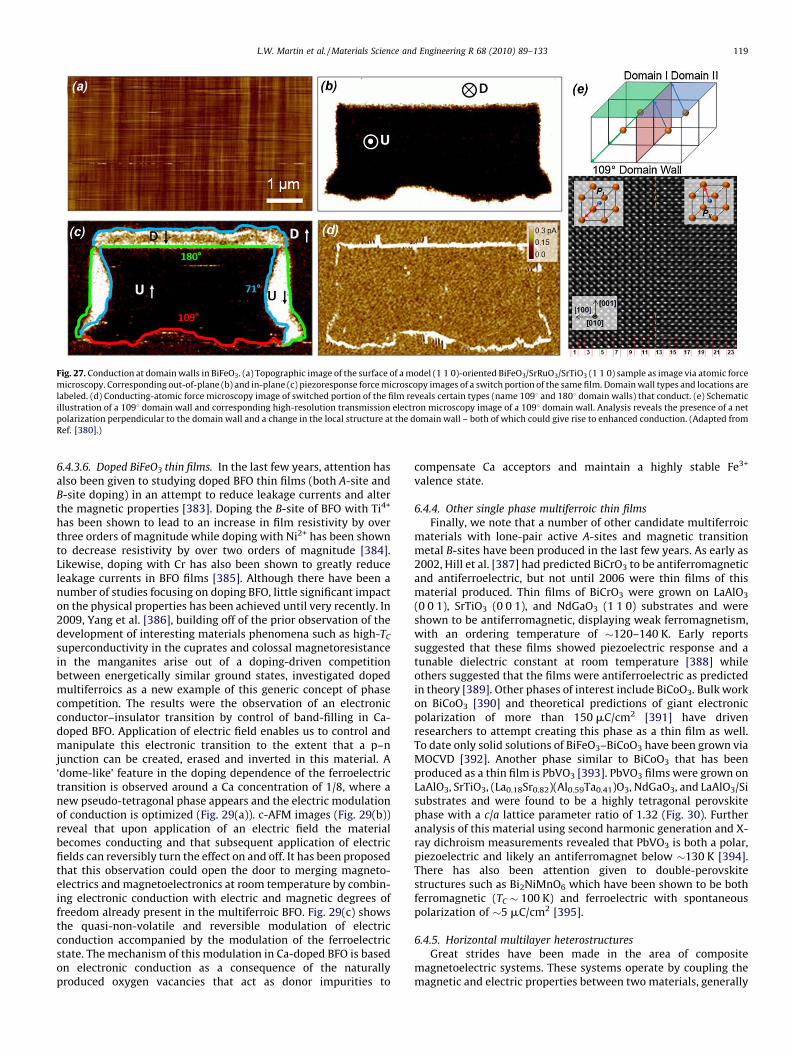
Fig. 27. Conduction at domain walls in BiFeO3. (a) Topographic image of the surface of a model (1 1 0)-oriented BiFeO3/SrRuO3/SrTiO3 (1 1 0) sample as image via atomic force
microscopy. Corresponding out-of-plane (b) and in-plane (c) piezoresponse force microscopy images of a switch portion of the same film. Domain wall types and locations are
labeled. (d) Conducting-atomic force microscopy image of switched portion of the film reveals certain types (name 1098 and 1808 domain walls) that conduct. (e) Schematic
illustration of a 1098 domain wall and corresponding high-resolution transmission electron microscopy image of a 1098 domain wall. Analysis reveals the presence of a net
polarization perpendicular to the domain wall and a change in the local structure at the domain wall – both of which could give rise to enhanced conduction. (Adapted from
Ref. [380].)
L.W. Martin et al. / Materials Science and Engineering R 68 (2010) 89–133 119
6.4.3.6. Doped BiFeO3 thin films. In the last few years, attention hasalso been given to studying doped BFO thin films (both A-site andB-site doping) in an attempt to reduce leakage currents and alterthe magnetic properties [383]. Doping the B-site of BFO with Ti4+
has been shown to lead to an increase in film resistivity by overthree orders of magnitude while doping with Ni2+ has been shownto decrease resistivity by over two orders of magnitude [384].Likewise, doping with Cr has also been shown to greatly reduceleakage currents in BFO films [385]. Although there have been anumber of studies focusing on doping BFO, little significant impacton the physical properties has been achieved until very recently. In2009, Yang et al. [386], building off of the prior observation of thedevelopment of interesting materials phenomena such as high-TC
superconductivity in the cuprates and colossal magnetoresistancein the manganites arise out of a doping-driven competitionbetween energetically similar ground states, investigated dopedmultiferroics as a new example of this generic concept of phasecompetition. The results were the observation of an electronicconductor–insulator transition by control of band-filling in Ca-doped BFO. Application of electric field enables us to control andmanipulate this electronic transition to the extent that a p–njunction can be created, erased and inverted in this material. A‘dome-like’ feature in the doping dependence of the ferroelectrictransition is observed around a Ca concentration of 1/8, where anew pseudo-tetragonal phase appears and the electric modulationof conduction is optimized (Fig. 29(a)). c-AFM images (Fig. 29(b))reveal that upon application of an electric field the materialbecomes conducting and that subsequent application of electricfields can reversibly turn the effect on and off. It has been proposedthat this observation could open the door to merging magneto-electrics and magnetoelectronics at room temperature by combin-ing electronic conduction with electric and magnetic degrees offreedom already present in the multiferroic BFO. Fig. 29(c) showsthe quasi-non-volatile and reversible modulation of electricconduction accompanied by the modulation of the ferroelectricstate. The mechanism of this modulation in Ca-doped BFO is basedon electronic conduction as a consequence of the naturallyproduced oxygen vacancies that act as donor impurities to
compensate Ca acceptors and maintain a highly stable Fe3+
valence state.
6.4.4. Other single phase multiferroic thin films
Finally, we note that a number of other candidate multiferroicmaterials with lone-pair active A-sites and magnetic transitionmetal B-sites have been produced in the last few years. As early as2002, Hill et al. [387] had predicted BiCrO3 to be antiferromagneticand antiferroelectric, but not until 2006 were thin films of thismaterial produced. Thin films of BiCrO3 were grown on LaAlO3
(0 0 1), SrTiO3 (0 0 1), and NdGaO3 (1 1 0) substrates and wereshown to be antiferromagnetic, displaying weak ferromagnetism,with an ordering temperature of �120–140 K. Early reportssuggested that these films showed piezoelectric response and atunable dielectric constant at room temperature [388] whileothers suggested that the films were antiferroelectric as predictedin theory [389]. Other phases of interest include BiCoO3. Bulk workon BiCoO3 [390] and theoretical predictions of giant electronicpolarization of more than 150 mC/cm2 [391] have drivenresearchers to attempt creating this phase as a thin film as well.To date only solid solutions of BiFeO3–BiCoO3 have been grown viaMOCVD [392]. Another phase similar to BiCoO3 that has beenproduced as a thin film is PbVO3 [393]. PbVO3 films were grown onLaAlO3, SrTiO3, (La0.18Sr0.82)(Al0.59Ta0.41)O3, NdGaO3, and LaAlO3/Sisubstrates and were found to be a highly tetragonal perovskitephase with a c/a lattice parameter ratio of 1.32 (Fig. 30). Furtheranalysis of this material using second harmonic generation and X-ray dichroism measurements revealed that PbVO3 is both a polar,piezoelectric and likely an antiferromagnet below �130 K [394].There has also been attention given to double-perovskitestructures such as Bi2NiMnO6 which have been shown to be bothferromagnetic (TC � 100 K) and ferroelectric with spontaneouspolarization of �5 mC/cm2 [395].
6.4.5. Horizontal multilayer heterostructures
Great strides have been made in the area of compositemagnetoelectric systems. These systems operate by coupling themagnetic and electric properties between two materials, generally
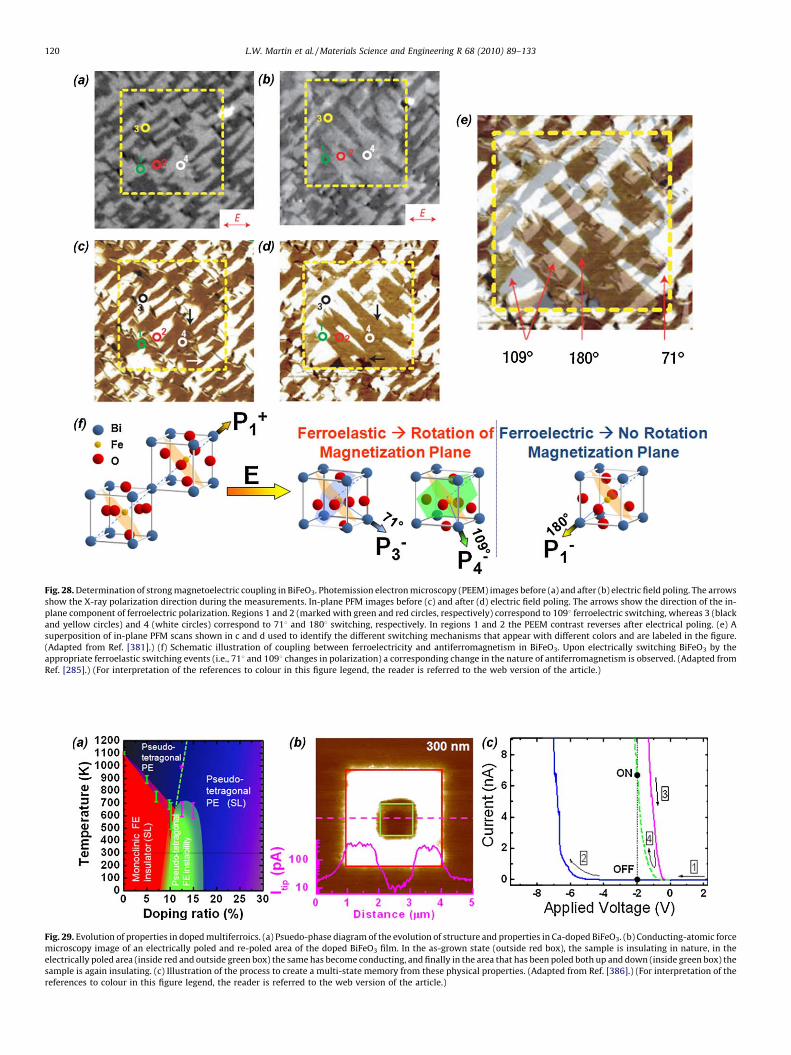
Fig. 28. Determination of strong magnetoelectric coupling in BiFeO3. Photemission electron microscopy (PEEM) images before (a) and after (b) electric field poling. The arrows
show the X-ray polarization direction during the measurements. In-plane PFM images before (c) and after (d) electric field poling. The arrows show the direction of the in-
plane component of ferroelectric polarization. Regions 1 and 2 (marked with green and red circles, respectively) correspond to 1098 ferroelectric switching, whereas 3 (black
and yellow circles) and 4 (white circles) correspond to 718 and 1808 switching, respectively. In regions 1 and 2 the PEEM contrast reverses after electrical poling. (e) A
superposition of in-plane PFM scans shown in c and d used to identify the different switching mechanisms that appear with different colors and are labeled in the figure.
(Adapted from Ref. [381].) (f) Schematic illustration of coupling between ferroelectricity and antiferromagnetism in BiFeO3. Upon electrically switching BiFeO3 by the
appropriate ferroelastic switching events (i.e., 718 and 1098 changes in polarization) a corresponding change in the nature of antiferromagnetism is observed. (Adapted from
Ref. [285].) (For interpretation of the references to colour in this figure legend, the reader is referred to the web version of the article.)
Fig. 29. Evolution of properties in doped multiferroics. (a) Psuedo-phase diagram of the evolution of structure and properties in Ca-doped BiFeO3. (b) Conducting-atomic force
microscopy image of an electrically poled and re-poled area of the doped BiFeO3 film. In the as-grown state (outside red box), the sample is insulating in nature, in the
electrically poled area (inside red and outside green box) the same has become conducting, and finally in the area that has been poled both up and down (inside green box) the
sample is again insulating. (c) Illustration of the process to create a multi-state memory from these physical properties. (Adapted from Ref. [386].) (For interpretation of the
references to colour in this figure legend, the reader is referred to the web version of the article.)
L.W. Martin et al. / Materials Science and Engineering R 68 (2010) 89–133120
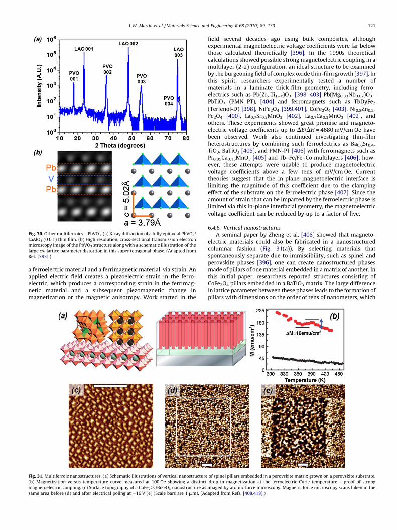
Fig. 30. Other multiferroics – PbVO3. (a) X-ray diffraction of a fully epitaxial PbVO3/
LaAlO3 (0 0 1) thin film. (b) High resolution, cross-sectional transmission electron
microscopy image of the PbVO3 structure along with a schematic illustration of the
large c/a lattice parameter distortion in this super tetragonal phase. (Adapted from
Ref. [393].)
L.W. Martin et al. / Materials Science and Engineering R 68 (2010) 89–133 121
a ferroelectric material and a ferrimagnetic material, via strain. Anapplied electric field creates a piezoelectric strain in the ferro-electric, which produces a corresponding strain in the ferrimag-netic material and a subsequent piezomagnetic change inmagnetization or the magnetic anisotropy. Work started in the
Fig. 31. Multiferroic nanostructures. (a) Schematic illustrations of vertical nanostructure
(b) Magnetization versus temperature curve measured at 100 Oe showing a distinct
magnetoelectric coupling. (c) Surface topography of a CoFe2O4/BiFeO3 nanostructure as
same area before (d) and after electrical poling at �16 V (e) (Scale bars are 1 mm). (Ad
field several decades ago using bulk composites, althoughexperimental magnetoelectric voltage coefficients were far belowthose calculated theoretically [396]. In the 1990s theoreticalcalculations showed possible strong magnetoelectric coupling in amultilayer (2-2) configuration; an ideal structure to be examinedby the burgeoning field of complex oxide thin-film growth [397]. Inthis spirit, researchers experimentally tested a number ofmaterials in a laminate thick-film geometry, including ferro-electrics such as Pb(Zrx,Ti1�x)O3, [398–403] Pb(Mg0.33Nb0.67)O3–PbTiO3 (PMN–PT), [404] and ferromagnets such as TbDyFe2
(Terfenol-D) [398], NiFe2O4 [399,401], CoFe2O4 [403], Ni0.8Zn0.2-
Fe2O4 [400], La0.7Sr0.3MnO3 [402], La0.7Ca0.3MnO3 [402], andothers. These experiments showed great promise and magneto-electric voltage coefficients up to DE/DH = 4680 mV/cm Oe havebeen observed. Work also continued investigating thin-filmheterostructures by combining such ferroelectrics as Ba0.6Sr0.4-
TiO3, BaTiO3 [405], and PMN-PT [406] with ferromagnets such asPr0.85Ca0.15MnO3 [405] and Tb–Fe/Fe–Co multilayers [406]; how-ever, these attempts were unable to produce magnetoelectricvoltage coefficients above a few tens of mV/cm Oe. Currenttheories suggest that the in-plane magnetoelectric interface islimiting the magnitude of this coefficient due to the clampingeffect of the substrate on the ferroelectric phase [407]. Since theamount of strain that can be imparted by the ferroelectric phase islimited via this in-plane interfacial geometry, the magnetoelectricvoltage coefficient can be reduced by up to a factor of five.
6.4.6. Vertical nanostructures
A seminal paper by Zheng et al. [408] showed that magneto-electric materials could also be fabricated in a nanostructuredcolumnar fashion (Fig. 31(a)). By selecting materials thatspontaneously separate due to immiscibility, such as spinel andperovskite phases [396], one can create nanostructured phasesmade of pillars of one material embedded in a matrix of another. Inthis initial paper, researchers reported structures consisting ofCoFe2O4 pillars embedded in a BaTiO3 matrix. The large differencein lattice parameter between these phases leads to the formation ofpillars with dimensions on the order of tens of nanometers, which
of spinel pillars embedded in a perovskite matrix grown on a perovskite substrate.
drop in magnetization at the ferroelectric Curie temperature – proof of strong
imaged by atomic force microscopy. Magnetic force microscopy scans taken in the
apted from Refs. [408,418].)
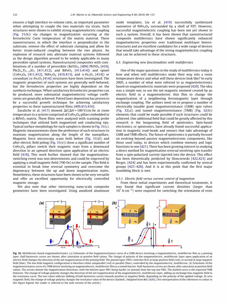
L.W. Martin et al. / Materials Science and Engineering R 68 (2010) 89–133122
ensures a high interface-to-volume ratio, an important parameterwhen attempting to couple the two materials via strain. Suchstructures were shown to exhibit strong magnetoelectric coupling(Fig. 31(b)) via changes in magnetization occurring at theferroelectric Curie temperature of the matrix material. Thesenanostructures, in which the interface is perpendicular to thesubstrate, remove the effect of substrate clamping and allow forbetter strain-induced coupling between the two phases. Anexplosion of research into alternate material systems followedas the design algorithm proved to be widely applicable to manyperovskite-spinel systems. Nanostructured composites with com-binations of a number of perovskite (BaTiO3, [409] PbTiO3 [410],Pb(Zrx,Ti1�x)O3 [411,412], and BiFeO3 [413,414]) and spinel(CoFe2O4 [411,412], NiFe2O4 [410,413], and g-Fe2O3 [414]) orcorundum (a-Fe2O3 [414]) structures have been investigated. Themagnetic properties of such systems are generally well-behaved,but the ferroelectric properties are highly dependent on thesynthesis technique. When satisfactory ferroelectric properties canbe produced, more substantial magnetoelectric voltage coeffi-cients are generally achieved. Pulsed laser deposition has proven tobe a successful growth technique for achieving satisfactoryproperties in these nanostructured films [409,415,416].
Zavaliche et al. [417] showed DE/DH = 100 V/cm Oe at roomtemperature in a system comprised of CoFe2O4 pillars embedded ina BiFeO3 matrix. These films were analyzed with scanning probetechniques that utilized both magnetized and conducting tips.Typical surface morphology for such samples is shown in Fig. 31(c).Magnetic measurements show the preference of such structures tomaintain magnetization along the length of the nanopillars.Magnetic force microscopy scans both before (Fig. 31(d)) andafter electric field poling (Fig. 31(e)) show a significant number ofCoFe2O4 pillars switch their magnetic state from a downwarddirection to an upward direction upon application of an electricfield [418], This work further showed that the magnetization-switching event was non-deterministic and could be improved byapplying a small magnetic field (700 Oe) to the sample. This field isessential to break time reversal symmetry and overcome thedegeneracy between the up and down magnetization states.Nonetheless, these structures have been shown to be very versatileand offer an excellent opportunity for electrically controlledmagnetic storage.
We also note that other interesting nano-scale compositegeometries have been investigated. Using anodized aluminum
Fig. 32. Multiferroic-based magnetoelectronics. (a) Schematic of the magnetoresistance
layer. Half-hysteresis curves are shown, after saturation at positive field values. The ch
electric field changes the direction of the net magnetization of the pinning field. The pinn
field (blue). The low field magnetic configuration is therefore either antiparallel (red) or
magnetoresistance curve of a TMR device involving an magnetoelectric, multiferroic film
values. The arrows denote the magnetization directions, with the bottom layer FM1 bei
behavior. The change of voltage polarity changes the direction of the net magnetization o
the resistance curve. The two colors indicate shifting of half-hysteresis curves towards p
magnetic field, the change of voltage polarity changes the resistance value of the device (
this figure legend, the reader is referred to the web version of the article.)
oxide templates, Liu et al. [419] successfully synthesizednanowires of NiFe2O4 surrounded by a shell of PZT. However,successful magnetoelectric coupling has been not yet shown insuch a system. Overall, it has been shown that nanostructuredcomposite multiferroics have shown significantly enhancedmagnetoelectric properties over traditional multilayer hetero-structures and are excellent candidates for a wide range of devicesthat would take advantage of the strong magnetoelectric couplingthat can be achieved in these structures.
6.5. Engineering new functionalities with multiferroics
One of the major questions in the study of multiferroics today ishow and when will multiferroics make their way into a roomtemperature device and what will these devices look like? In early2005, a number of what were referred to as magnetoelectronics
based on magnetoelectric materials were proposed [420]. The ideawas a simple one, to use the net magnetic moment created by anelectric field in a magnetoelectric thin film to change themagnetization of a neighboring ferromagnetic layer throughexchange coupling. The authors went on to propose a number ofelectrically tunable giant magnetoresistance (GMR) spin valves(Fig. 32(a)) and tunnel magnetoresistance (TMR) (Fig. 32(b))elements that could be made possible if such structures could beachieved. One additional field that could be greatly affected by thisresearch is the burgeoning field of spintronics. Spin-basedelectronics, or spintronics, have already found successful applica-tion in magnetic read-heads and sensors that take advantage ofGMR and TMR effects. The future of spintronics is partially focusedon evolving beyond passive magnetoelectronic components, likethose used today, to devices which combine memory and logicfunctions in one [421]. There has been growing interest in studyinga direct method for magnetization reversal involving spin transferfrom a spin-polarized current injected into the device. This effecthas been theoretically predicted by Slonczewski [422,423] andBerger, [424] and has been experimentally confirmed by severalgroups [425–428]. And it is at this point that the first majorstumbling block is met.
6.5.1. Electric field versus current control of magnetism
From these initial experiments and theoretical treatments, itwas found that significant current densities (larger than107 A cm�2) were required for switching the orientation of even
curve of a GMR device involving a magnetoelectric, multiferroic film as a pinning
ange of polarity of the magnetoelectric, multiferroic layer upon application of an
ed layer (FM1) switches first at large positive field (red), or second at large negative
parallel (blue), controlled by the magnetoelectric, multiferroic. (b) Schematic of the
as a tunnel barrier. Half-hysteresis curves are shown, after saturation at positive field
ng harder (or pinned) than the top one FM2. The dashed curve is the expected TMR
f the magnetoelectric, multiferroic layer, adding an exchange bias magnetic field to
ositive or negative fields, depending on the polarity of the applied voltage. At zero
dashed). (Adapted from Ref. [420].) (For interpretation of the references to colour in
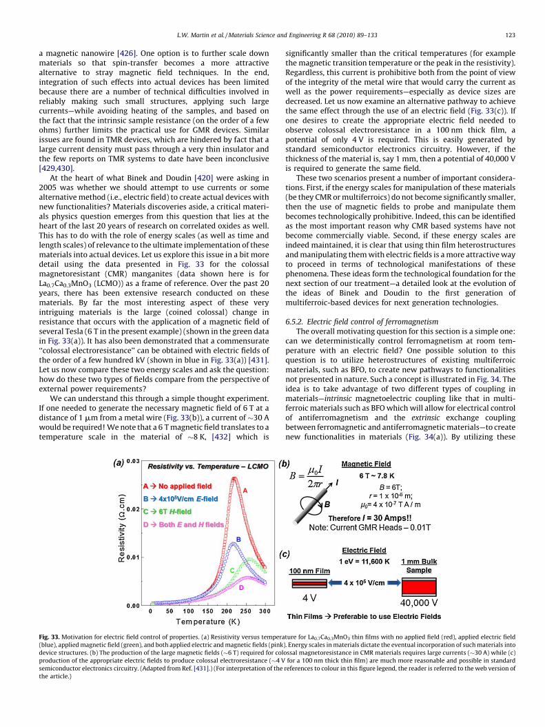
L.W. Martin et al. / Materials Science and Engineering R 68 (2010) 89–133 123
a magnetic nanowire [426]. One option is to further scale downmaterials so that spin-transfer becomes a more attractivealternative to stray magnetic field techniques. In the end,integration of such effects into actual devices has been limitedbecause there are a number of technical difficulties involved inreliably making such small structures, applying such largecurrents—while avoiding heating of the samples, and based onthe fact that the intrinsic sample resistance (on the order of a fewohms) further limits the practical use for GMR devices. Similarissues are found in TMR devices, which are hindered by fact that alarge current density must pass through a very thin insulator andthe few reports on TMR systems to date have been inconclusive[429,430].
At the heart of what Binek and Doudin [420] were asking in2005 was whether we should attempt to use currents or somealternative method (i.e., electric field) to create actual devices withnew functionalities? Materials discoveries aside, a critical materi-als physics question emerges from this question that lies at theheart of the last 20 years of research on correlated oxides as well.This has to do with the role of energy scales (as well as time andlength scales) of relevance to the ultimate implementation of thesematerials into actual devices. Let us explore this issue in a bit moredetail using the data presented in Fig. 33 for the colossalmagnetoresistant (CMR) manganites (data shown here is forLa0.7Ca0.3MnO3 (LCMO)) as a frame of reference. Over the past 20years, there has been extensive research conducted on thesematerials. By far the most interesting aspect of these veryintriguing materials is the large (coined colossal) change inresistance that occurs with the application of a magnetic field ofseveral Tesla (6 T in the present example) (shown in the green datain Fig. 33(a)). It has also been demonstrated that a commensurate‘‘colossal electroresistance’’ can be obtained with electric fields ofthe order of a few hundred kV (shown in blue in Fig. 33(a)) [431].Let us now compare these two energy scales and ask the question:how do these two types of fields compare from the perspective ofexternal power requirements?
We can understand this through a simple thought experiment.If one needed to generate the necessary magnetic field of 6 T at adistance of 1 mm from a metal wire (Fig. 33(b)), a current of �30 Awould be required! We note that a 6 T magnetic field translates to atemperature scale in the material of �8 K, [432] which is
Fig. 33. Motivation for electric field control of properties. (a) Resistivity versus tempera
(blue), applied magnetic field (green), and both applied electric and magnetic fields (pink
device structures. (b) The production of the large magnetic fields (�6 T) required for col
production of the appropriate electric fields to produce colossal electroresistance (�4 V
semiconductor electronics circuitry. (Adapted from Ref. [431].) (For interpretation of the
the article.)
significantly smaller than the critical temperatures (for examplethe magnetic transition temperature or the peak in the resistivity).Regardless, this current is prohibitive both from the point of viewof the integrity of the metal wire that would carry the current aswell as the power requirements—especially as device sizes aredecreased. Let us now examine an alternative pathway to achievethe same effect through the use of an electric field (Fig. 33(c)). Ifone desires to create the appropriate electric field needed toobserve colossal electroresistance in a 100 nm thick film, apotential of only 4 V is required. This is easily generated bystandard semiconductor electronics circuitry. However, if thethickness of the material is, say 1 mm, then a potential of 40,000 Vis required to generate the same field.
These two scenarios present a number of important considera-tions. First, if the energy scales for manipulation of these materials(be they CMR or multiferroics) do not become significantly smaller,then the use of magnetic fields to probe and manipulate thembecomes technologically prohibitive. Indeed, this can be identifiedas the most important reason why CMR based systems have notbecome commercially viable. Second, if these energy scales areindeed maintained, it is clear that using thin film heterostructuresand manipulating them with electric fields is a more attractive wayto proceed in terms of technological manifestations of thesephenomena. These ideas form the technological foundation for thenext section of our treatment—a detailed look at the evolution ofthe ideas of Binek and Doudin to the first generation ofmultiferroic-based devices for next generation technologies.
6.5.2. Electric field control of ferromagnetism
The overall motivating question for this section is a simple one:can we deterministically control ferromagnetism at room tem-perature with an electric field? One possible solution to thisquestion is to utilize heterostructures of existing multiferroicmaterials, such as BFO, to create new pathways to functionalitiesnot presented in nature. Such a concept is illustrated in Fig. 34. Theidea is to take advantage of two different types of coupling inmaterials—intrinsic magnetoelectric coupling like that in multi-ferroic materials such as BFO which will allow for electrical controlof antiferromagnetism and the extrinsic exchange couplingbetween ferromagnetic and antiferromagnetic materials—to createnew functionalities in materials (Fig. 34(a)). By utilizing these
ture for La0.7Ca0.3MnO3 thin films with no applied field (red), applied electric field
). Energy scales in materials dictate the eventual incorporation of such materials into
ossal magnetoresistance in CMR materials requires large currents (�30 A) while (c)
for a 100 nm thick thin film) are much more reasonable and possible in standard
references to colour in this figure legend, the reader is referred to the web version of
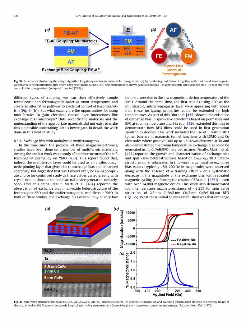
Fig. 34. Schematics illustrating the design algorithm for gaining electrical control of ferromagnetism. (a) By combining multiferroics together with traditional ferromagnets,
we can create heterostructures that might have new functionalities. (b) These structure rely on two types of coupling – magnetoelectric and exchange bias – to gain electrical
control of ferromagnetism. (Adapted from Ref. [285].)
L.W. Martin et al. / Materials Science and Engineering R 68 (2010) 89–133124
different types of coupling we can then effectively coupleferroelectric and ferromagnetic order at room temperature andcreate an alternative pathway to electrical control of ferromagnet-ism (Fig. 34(b)). But what exactly are the opportunities for usingmultiferroics to gain electrical control over interactions likeexchange bias anisotropy? Until recently the materials and theunderstanding of the appropriate materials did not exist to makethis a plausible undertaking. Let us investigate, in detail, the workdone in this field of study.
6.5.3. Exchange bias with multiferroic antiferromagnets
In the time since the proposal of these magnetoelectronics,studies have been done on a number of multiferroic materials.Among the earliest work was a study of heterostructures of the softferromagnet permalloy on YMO [433]. This report found that,indeed, the multiferroic layer could be used as an antiferromag-netic pinning layer that gives rise to exchange bias and enhancedcoercivity, but suggested that YMO would likely be an inappropri-ate choice for continued study as these values varied greatly withcrystal orientation and rendered actual device generation unlikely.Soon after this initial result, Marti et al. [434] reported theobservation of exchange bias in all-oxide heterostructure of theferromagnet SRO and the antiferromagnetic, multiferroic YMO. Inboth of these studies, the exchange bias existed only at very low
Fig. 35. Spin valve structures based on Co0.9Fe0.1/Cu/Co0.9Fe0.1/BiFeO3 heterostructures.
the actual device. (b) Magnetic hysteresis loops of spin valve structures. (c) Current-in
temperatures due to the low magnetic ordering temperature of theYMO. Around the same time, the first studies using BFO as themultiferroic, antiferromagnetic layer were appearing with hopesthat these intriguing properties could be extended to hightemperatures. As part of this Dho et al. [435] showed the existenceof exchange bias in spin-valve structures based on permalloy andBFO at room temperature and Bea et al. [436] extended this idea todemonstrate how BFO films could be used in first generationspintronics devices. This work included the use of ultrathin BFOtunnel barriers in magnetic tunnel junctions with LSMO and Coelectrodes where positive TMR up to�30% was observed at 3K andalso demonstrated that room temperature exchange bias could begenerated using CoFeB/BFO heterostructures. Finally, Martin et al.[437] reported the growth and characterization of exchange biasand spin valve heterostructures based on Co0.9Fe0.1/BFO hetero-structures on Si substrates. In this work large negative exchangebias values (typically 150–200 Oe in magnitude) were observedalong with the absence of a training effect – or a systematicdecrease in the magnitude of the exchange bias with repeatedmagnetic cycling (confirming the results of Bea et al. [436]) – evenwith over 14,000 magnetic cycles. This work also demonstratedroom temperature magnetoresistance of �2.25% for spin valvestructures of 2.5 nm CoFe/2 nm Cu/5 nm CoFe/100 nm BFO(Fig. 35). What these initial studies established was that exchange
(a) Schematic illustration and scanning transmission electron microscopy image of
-plane magnetoresistance measurements. (Adapted from Ref. [437].)
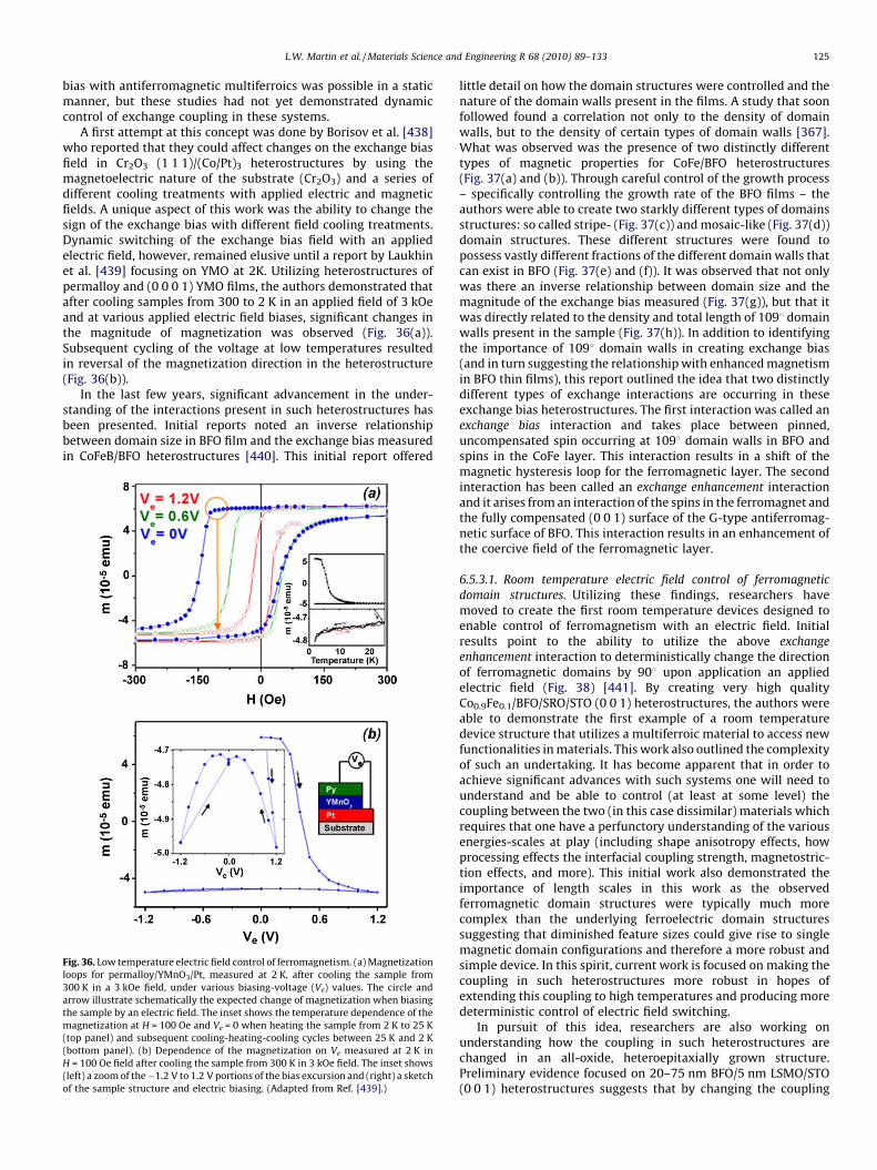
L.W. Martin et al. / Materials Science and Engineering R 68 (2010) 89–133 125
bias with antiferromagnetic multiferroics was possible in a staticmanner, but these studies had not yet demonstrated dynamiccontrol of exchange coupling in these systems.
A first attempt at this concept was done by Borisov et al. [438]who reported that they could affect changes on the exchange biasfield in Cr2O3 (1 1 1)/(Co/Pt)3 heterostructures by using themagnetoelectric nature of the substrate (Cr2O3) and a series ofdifferent cooling treatments with applied electric and magneticfields. A unique aspect of this work was the ability to change thesign of the exchange bias with different field cooling treatments.Dynamic switching of the exchange bias field with an appliedelectric field, however, remained elusive until a report by Laukhinet al. [439] focusing on YMO at 2K. Utilizing heterostructures ofpermalloy and (0 0 0 1) YMO films, the authors demonstrated thatafter cooling samples from 300 to 2 K in an applied field of 3 kOeand at various applied electric field biases, significant changes inthe magnitude of magnetization was observed (Fig. 36(a)).Subsequent cycling of the voltage at low temperatures resultedin reversal of the magnetization direction in the heterostructure(Fig. 36(b)).
In the last few years, significant advancement in the under-standing of the interactions present in such heterostructures hasbeen presented. Initial reports noted an inverse relationshipbetween domain size in BFO film and the exchange bias measuredin CoFeB/BFO heterostructures [440]. This initial report offered
Fig. 36. Low temperature electric field control of ferromagnetism. (a) Magnetization
loops for permalloy/YMnO3/Pt, measured at 2 K, after cooling the sample from
300 K in a 3 kOe field, under various biasing-voltage (Ve) values. The circle and
arrow illustrate schematically the expected change of magnetization when biasing
the sample by an electric field. The inset shows the temperature dependence of the
magnetization at H = 100 Oe and Ve = 0 when heating the sample from 2 K to 25 K
(top panel) and subsequent cooling-heating-cooling cycles between 25 K and 2 K
(bottom panel). (b) Dependence of the magnetization on Ve measured at 2 K in
H = 100 Oe field after cooling the sample from 300 K in 3 kOe field. The inset shows
(left) a zoom of the�1.2 V to 1.2 V portions of the bias excursion and (right) a sketch
of the sample structure and electric biasing. (Adapted from Ref. [439].)
little detail on how the domain structures were controlled and thenature of the domain walls present in the films. A study that soonfollowed found a correlation not only to the density of domainwalls, but to the density of certain types of domain walls [367].What was observed was the presence of two distinctly differenttypes of magnetic properties for CoFe/BFO heterostructures(Fig. 37(a) and (b)). Through careful control of the growth process– specifically controlling the growth rate of the BFO films – theauthors were able to create two starkly different types of domainsstructures: so called stripe- (Fig. 37(c)) and mosaic-like (Fig. 37(d))domain structures. These different structures were found topossess vastly different fractions of the different domain walls thatcan exist in BFO (Fig. 37(e) and (f)). It was observed that not onlywas there an inverse relationship between domain size and themagnitude of the exchange bias measured (Fig. 37(g)), but that itwas directly related to the density and total length of 1098 domainwalls present in the sample (Fig. 37(h)). In addition to identifyingthe importance of 1098 domain walls in creating exchange bias(and in turn suggesting the relationship with enhanced magnetismin BFO thin films), this report outlined the idea that two distinctlydifferent types of exchange interactions are occurring in theseexchange bias heterostructures. The first interaction was called anexchange bias interaction and takes place between pinned,uncompensated spin occurring at 1098 domain walls in BFO andspins in the CoFe layer. This interaction results in a shift of themagnetic hysteresis loop for the ferromagnetic layer. The secondinteraction has been called an exchange enhancement interactionand it arises from an interaction of the spins in the ferromagnet andthe fully compensated (0 0 1) surface of the G-type antiferromag-netic surface of BFO. This interaction results in an enhancement ofthe coercive field of the ferromagnetic layer.
6.5.3.1. Room temperature electric field control of ferromagnetic
domain structures. Utilizing these findings, researchers havemoved to create the first room temperature devices designed toenable control of ferromagnetism with an electric field. Initialresults point to the ability to utilize the above exchange
enhancement interaction to deterministically change the directionof ferromagnetic domains by 908 upon application an appliedelectric field (Fig. 38) [441]. By creating very high qualityCo0.9Fe0.1/BFO/SRO/STO (0 0 1) heterostructures, the authors wereable to demonstrate the first example of a room temperaturedevice structure that utilizes a multiferroic material to access newfunctionalities in materials. This work also outlined the complexityof such an undertaking. It has become apparent that in order toachieve significant advances with such systems one will need tounderstand and be able to control (at least at some level) thecoupling between the two (in this case dissimilar) materials whichrequires that one have a perfunctory understanding of the variousenergies-scales at play (including shape anisotropy effects, howprocessing effects the interfacial coupling strength, magnetostric-tion effects, and more). This initial work also demonstrated theimportance of length scales in this work as the observedferromagnetic domain structures were typically much morecomplex than the underlying ferroelectric domain structuressuggesting that diminished feature sizes could give rise to singlemagnetic domain configurations and therefore a more robust andsimple device. In this spirit, current work is focused on making thecoupling in such heterostructures more robust in hopes ofextending this coupling to high temperatures and producing moredeterministic control of electric field switching.
In pursuit of this idea, researchers are also working onunderstanding how the coupling in such heterostructures arechanged in an all-oxide, heteroepitaxially grown structure.Preliminary evidence focused on 20–75 nm BFO/5 nm LSMO/STO(0 0 1) heterostructures suggests that by changing the coupling

Fig. 37. Domain control of exchange bias. Room temperature magnetic properties for heterostructures exhibiting (a) exchange enhancement and (b) exchange bias properties.
In-plane and out-of-plane (inset) PFM contrast for typical BiFeO3 films that exhibit (c) exchange enhancement and (d) exchange bias, respectively. Detailed domain wall
analysis for (e) stripe-like and (f) mosaic-like BFO films. (g) Dependence of exchange bias field on domain size for Co0.9Fe0.1/BiFeO3 heterostructures grown on mosaic-like
(blue) and stripe-like (red) BFO films. (h) Exchange bias field of the same samples here graphed as a function of the total length of 1098 domain walls/sample surface area in
5 � 5 mm samples. (Adapted from Ref. [367].) (For interpretation of the references to colour in this figure legend, the reader is referred to the web version of the article.)
L.W. Martin et al. / Materials Science and Engineering R 68 (2010) 89–133126
from being direct in nature to indirect across an interfacepossessing a continuous chemical structure (i.e., Mn–O–Fe bondsthat extend across the interface) complex interactions can occur(Fig. 39) [442]. This work has shown that, due to the strongcoupling between spin, lattice, orbital, and charge degrees-of-freedom in these oxide materials, interactions across theseinterfaces can become quite complex with changes in bond angleand length, electron density, orbital order, and more dictating theeffects observed. In the end, it is such structures, however, thatmight represent the ultimate manifestation of new functionality ifone can engineer and control these different degrees-of-freedom tosome effect.
Fig. 38. Electric field control of ferromagnetic domain structures at room temperature.
(top) and corresponding photoemission electron microscopy image of ferromagnetic d
electric field in the (a) as-grown state, (b) after application of an electric field, and
demonstration of reversible electric field control of ferromagnetic domain structures a
6.6. Advanced multiferroic-based devices
In 2007, Scott offered a brief, but elegant summary of wheremultiferroic-based devices, especially memory applications, mightmake an impact [443]. It is important to note that althoughferroelectric random access memories (FeRAMs) have achievedfast access speeds (5 ns) and high densities (64 Mb) in a number ofdifferent materials, they remain limited by the need for adestructive read and reset operation. By comparison, magneticrandom access memories (MRAMs) have been lagging far behind,although Freescale Corporation reported commercial productionin 2006 of a smaller MRAM for testing. The appeal of multiferroics
In-plane piezoresponse force microscopy images of ferroelectric domain structure
omain structure (bottom) of Co0.9Fe0.1 features on BiFeO3 as a function of applied
(c) following application of the opposite electric field. This represents the first
t room temperature. (Adapted from Ref. [441].)
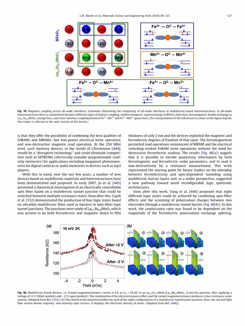
Fig. 39. Magnetic coupling across all-oxide interfaces. Schematic illustrating the complexity of all-oxide interfaces in multiferroic-based heterostructures. In all-oxide
heterostructures there is competition between different types of indirect coupling: antiferromagnetic superexchange in BiFeO3 (blue box), ferromagnetic double exchange in
La0.7Sr0.3MnO3 (orange box), and cross-interface coupling between Fe3+–Mn3+ and Fe3+–Mn4+ (green box). (For interpretation of the references to colour in this figure legend,
the reader is referred to the web version of the article.)
L.W. Martin et al. / Materials Science and Engineering R 68 (2010) 89–133 127
is that they offer the possibility of combining the best qualities ofFeRAMs and MRAMs: fast low-power electrical write operation,and non-destructive magnetic read operation. At the 256 Mbitlevel, such memory devices, in the words of Christensen [444],would be a ‘‘disruptive technology’’ and could eliminate competi-tion such as EEPROMs (electrically erasable programmable read-only memories) for applications including megapixel photomem-ories for digital cameras or audio memories in devices such as mp3players.
With this in mind, over the last few years, a number of newdevices based on multiferroic materials and heterostructures havebeen demonstrated and proposed. In early 2007, Ju et al. [445]presented a theoretical investigation of an electrically controllablespin filter based on a multiferroic tunnel junction that could beswitched between multiple resistance states. Soon after this, Gajeket al. [332] demonstrated the production of four logic states basedon ultrathin multiferroic films used as barriers in spin-filter-typetunnel junctions. The junctions were made of La0.1Bi0.9MnO3 whichwas proven to be both ferroelectric and magnetic down to film
Fig. 40. Multiferroic-based devices. (a) Tunnel magnetoresistance curves at 4 K at Vdc
voltage of +2 V (filled symbols) and�2 V (open symbols). The combination of the electro
system. (Adapted from Ref. [332].) (b) The sketch of the potential profiles for each of the
blue arrows denote majority- and minority-spin carriers, D displays the electronic den
thickness of only 2 nm and the devices exploited the magnetic andferroelectric degrees of freedom of that layer. The ferromagnetismpermitted read operations reminiscent of MRAM and the electricalswitching evoked FeRAM write operations without the need fordestructive ferroelectric readout. The results (Fig. 40(a)) suggestthat it is possible to encode quaternary information by bothferromagnetic and ferroelectric order parameters, and to read itnon-destructively by a resistance measurement. This workrepresented the starting point for future studies on the interplaybetween ferroelectricity and spin-dependent tunneling usingmultiferroic barrier layers and, in a wider perspective, suggesteda new pathway toward novel reconfigurable logic spintronicarchitectures.
Soon after this work, Yang et al. [446] proposed that eightdifferent logic states could be achieved by combining spin-filtereffects and the screening of polarization charges between twoelectrodes through a multiferroic tunnel barrier (Fig. 40(b)). In thiswork, the conductance ratio was found to be dependent on themagnitude of the ferroelectric polarization, exchange splitting,
= 10 mV in an La2/3Sr1/3MnO3/La0.1Bi0.9MnO3 (2 nm)/Au junction, after applying a
resistance effect and the tunnel magnetoresistance produces a four-resistance-state
eight configurations of a multiferroic-based tunnel junction. Here, the red and light
sity of states. (Adapted from Ref. [446]).
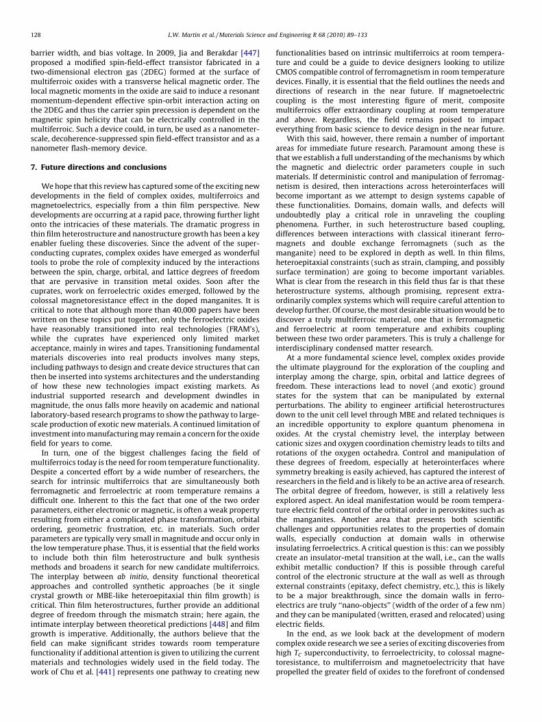
L.W. Martin et al. / Materials Science and Engineering R 68 (2010) 89–133128
barrier width, and bias voltage. In 2009, Jia and Berakdar [447]proposed a modified spin-field-effect transistor fabricated in atwo-dimensional electron gas (2DEG) formed at the surface ofmultiferroic oxides with a transverse helical magnetic order. Thelocal magnetic moments in the oxide are said to induce a resonantmomentum-dependent effective spin-orbit interaction acting onthe 2DEG and thus the carrier spin precession is dependent on themagnetic spin helicity that can be electrically controlled in themultiferroic. Such a device could, in turn, be used as a nanometer-scale, decoherence-suppressed spin field-effect transistor and as ananometer flash-memory device.
7. Future directions and conclusions
We hope that this review has captured some of the exciting newdevelopments in the field of complex oxides, multiferroics andmagnetoelectrics, especially from a thin film perspective. Newdevelopments are occurring at a rapid pace, throwing further lightonto the intricacies of these materials. The dramatic progress inthin film heterostructure and nanostructure growth has been a keyenabler fueling these discoveries. Since the advent of the super-conducting cuprates, complex oxides have emerged as wonderfultools to probe the role of complexity induced by the interactionsbetween the spin, charge, orbital, and lattice degrees of freedomthat are pervasive in transition metal oxides. Soon after thecuprates, work on ferroelectric oxides emerged, followed by thecolossal magnetoresistance effect in the doped manganites. It iscritical to note that although more than 40,000 papers have beenwritten on these topics put together, only the ferroelectric oxideshave reasonably transitioned into real technologies (FRAM’s),while the cuprates have experienced only limited marketacceptance, mainly in wires and tapes. Transitioning fundamentalmaterials discoveries into real products involves many steps,including pathways to design and create device structures that canthen be inserted into systems architectures and the understandingof how these new technologies impact existing markets. Asindustrial supported research and development dwindles inmagnitude, the onus falls more heavily on academic and nationallaboratory-based research programs to show the pathway to large-scale production of exotic new materials. A continued limitation ofinvestment into manufacturing may remain a concern for the oxidefield for years to come.
In turn, one of the biggest challenges facing the field ofmultiferroics today is the need for room temperature functionality.Despite a concerted effort by a wide number of researchers, thesearch for intrinsic multiferroics that are simultaneously bothferromagnetic and ferroelectric at room temperature remains adifficult one. Inherent to this the fact that one of the two orderparameters, either electronic or magnetic, is often a weak propertyresulting from either a complicated phase transformation, orbitalordering, geometric frustration, etc. in materials. Such orderparameters are typically very small in magnitude and occur only inthe low temperature phase. Thus, it is essential that the field worksto include both thin film heterostructure and bulk synthesismethods and broadens it search for new candidate multiferroics.The interplay between ab initio, density functional theoreticalapproaches and controlled synthetic approaches (be it singlecrystal growth or MBE-like heteroepitaxial thin film growth) iscritical. Thin film heterostructures, further provide an additionaldegree of freedom through the mismatch strain; here again, theintimate interplay between theoretical predictions [448] and filmgrowth is imperative. Additionally, the authors believe that thefield can make significant strides towards room temperaturefunctionality if additional attention is given to utilizing the currentmaterials and technologies widely used in the field today. Thework of Chu et al. [441] represents one pathway to creating new
functionalities based on intrinsic multiferroics at room tempera-ture and could be a guide to device designers looking to utilizeCMOS compatible control of ferromagnetism in room temperaturedevices. Finally, it is essential that the field outlines the needs anddirections of research in the near future. If magnetoelectriccoupling is the most interesting figure of merit, compositemultiferroics offer extraordinary coupling at room temperatureand above. Regardless, the field remains poised to impacteverything from basic science to device design in the near future.
With this said, however, there remain a number of importantareas for immediate future research. Paramount among these isthat we establish a full understanding of the mechanisms by whichthe magnetic and dielectric order parameters couple in suchmaterials. If deterministic control and manipulation of ferromag-netism is desired, then interactions across heterointerfaces willbecome important as we attempt to design systems capable ofthese functionalities. Domains, domain walls, and defects willundoubtedly play a critical role in unraveling the couplingphenomena. Further, in such heterostructure based coupling,differences between interactions with classical itinerant ferro-magnets and double exchange ferromagnets (such as themanganite) need to be explored in depth as well. In thin films,heteroepitaxial constraints (such as strain, clamping, and possiblysurface termination) are going to become important variables.What is clear from the research in this field thus far is that theseheterostructure systems, although promising, represent extra-ordinarily complex systems which will require careful attention todevelop further. Of course, the most desirable situation would be todiscover a truly multiferroic material, one that is ferromagneticand ferroelectric at room temperature and exhibits couplingbetween these two order parameters. This is truly a challenge forinterdisciplinary condensed matter research.
At a more fundamental science level, complex oxides providethe ultimate playground for the exploration of the coupling andinterplay among the charge, spin, orbital and lattice degrees offreedom. These interactions lead to novel (and exotic) groundstates for the system that can be manipulated by externalperturbations. The ability to engineer artificial heterostructuresdown to the unit cell level through MBE and related techniques isan incredible opportunity to explore quantum phenomena inoxides. At the crystal chemistry level, the interplay betweencationic sizes and oxygen coordination chemistry leads to tilts androtations of the oxygen octahedra. Control and manipulation ofthese degrees of freedom, especially at heterointerfaces wheresymmetry breaking is easily achieved, has captured the interest ofresearchers in the field and is likely to be an active area of research.The orbital degree of freedom, however, is still a relatively lessexplored aspect. An ideal manifestation would be room tempera-ture electric field control of the orbital order in perovskites such asthe manganites. Another area that presents both scientificchallenges and opportunities relates to the properties of domainwalls, especially conduction at domain walls in otherwiseinsulating ferroelectrics. A critical question is this: can we possiblycreate an insulator-metal transition at the wall, i.e., can the wallsexhibit metallic conduction? If this is possible through carefulcontrol of the electronic structure at the wall as well as throughexternal constraints (epitaxy, defect chemistry, etc.), this is likelyto be a major breakthrough, since the domain walls in ferro-electrics are truly ‘‘nano-objects’’ (width of the order of a few nm)and they can be manipulated (written, erased and relocated) usingelectric fields.
In the end, as we look back at the development of moderncomplex oxide research we see a series of exciting discoveries fromhigh TC superconductivity, to ferroelectricity, to colossal magne-toresistance, to multiferroism and magnetoelectricity that havepropelled the greater field of oxides to the forefront of condensed
L.W. Martin et al. / Materials Science and Engineering R 68 (2010) 89–133 129
matter physics. The field today stands poised for another greatdiscovery that will usher in a new era of discovery. The diversefunctionality of oxide materials means that this breakthroughcould drive the field towards many of the major scientificquestions that face us today – from energy, to medicine, tocommunications, and beyond.
Acknowledgements
The authors acknowledge the support of the Director, Office ofBasic Energy Sciences, Materials Science Division of the U.S.Department of Energy under Contract No. DE-AC02-05CH11231and previous contracts, ONR-MURI under Grant No. E21-6RU-G4and previous contracts, and the Western Institute of Nanoelec-tronics program as well as significant intellectual and financialsupport from scientists and engineers at Intel. Over the past 8-10years, R.R. has also benefitted significantly through funding fromthe Office of Naval Research (through a MURI program from 2003-2008) as well as funding from the National Science Foundationduring his tenure at the University of Maryland, College Park.
References
[1] C.N.R. Rao, B. Raveau, Transition Metal Oxides, 2nd edn., Wiley-VCH, New York,1998.
[2] D. Norton, Mater. Sci. Eng. R 43 (2004) 139.[3] S.N. Ruddlesden, P. Popper, Acta. Crystallogr. 11 (1958) 54.[4] Y. Maeno, H. Hashimoto, K. Yoshida, S. Nishizaki, T. Fujita, J.G. Bednorz, F.
Lichtenberg, Nature 372 (1994) 532.[5] G. Cao, S. McCall, J.E. Crow, Phys. Rev. B 55 (1997) 672.[6] S. Ikeda, Y. Maeno, T. Fujita, Phys. Rev. B 57 (1998) 978; S. Ikeda, Y. Maeno,
Physica B 259–261, (1999) 947; S. Ikeda, Y. Maeno, M. Kosaka, Y. Uwatoko, Phys.Rev. B 62 (2000) 1.
[7] M. Imada, A. Fujimori, Y. Tokura, Rev. Mod. Phys. 70 (1998) 1039.[8] J.B. Goodenough, Prog. Solid State Chem. 5 (1971) 145.[9] D.G. Schlom, J.H. Haeni, J. Lettieri, C.D. Theis, W. Tian, J.C. Jiang, X.Q. Pan, Mater.
Sci. Eng. B 87 (2001) 282.[10] M. Ohring, Materials Science of Thin Films: Deposition and Structure, Academic
Press, San Francisco, 2002.[11] D.L. Smith, Thin-Film Deposition: Principles and Practice, McGraw Hill, San
Francisco, 1995.[12] D.B. Chrisey, G.K. Hubler, Pulsed Laser Deposition of Thin Films, John Wiley &
Sons, Inc., New York, 1994.[13] R. Eason, Pulsed Laser Deposition of Thin Films: Applications-Led Growth of
Functional Materials, John Wiley & Sons, Hoboken, NJ, 2007.[14] H.M. Christen, G. Eres, J. Phys. Condens. Matter 20 (2008) 264005.[15] G. Bednorz, K.A. Muller, Z. Phys. B 64 (1986) 189.[16] D. Dijkkamp, T. Venkatesan, X.D. Wu, S.A. Shaheen, N. Jisrawi, Y.H. Min-Lee, W.L.
McLean, M. Croft, Appl. Phys. Lett. 51 (1987) 619.[17] X.D. Wu, T. Venkatesan, A. Inam, X.X. Xi, Q. Li, W.L. McLean, C.C. Chang, D.M.
Hwang, R. Ramesh, L. Nazar, B. Wilkens, S.A. Schwartz, R.T. Ravi, J.A. Martinez, P.England, J.M. Tarascon, R.E. Muenchausen, S. Foltyn, R.C. Estler, R.C. Dye, A.R.Garcia, N.S. Nogar, Mater. Res. Soc. Symp. Proc. 191 (1990) 129.
[18] H.M. Smith, A.F. Turner, Appl. Opt. 4 (1965) 147.[19] H. Schwarz, H.A. Tourtellotte, J. Vac. Sci. Technol. 6 (1969) 373.[20] H. Christen, D.P. Norton, L.A. Gea, L.A. Boatner, Thin Solid Films 312 (1998) 156.[21] D.H. Kim, H.N. Lee, M.D. Biegalski, H.M. Christen, Appl. Phys. Lett. 91 (2007)
042906.[22] H.M. Christen, S.D. Silliman, K.S. Harshavardhan, Rev. Sci. Instrum. 72 (2001)
2673.[23] H.M. Christen, C.M. Rouleau, I. Ohkubo, H.Y. Zhai, H.N. Lee, S. Sathyamurthy, D.H.
Lowndes, Rev. Sci. Instrum. 74 (2003) 4058.[24] I. Ohkubo, H.M. Christen, S.V. Kalinin, C.M. Rouleau, D.H. Lowndes, Appl. Phys.
Lett. 84 (2004) 1350.[25] H.M. Christen, G.E. Jellison Jr., I. Ohkubo, S. Huang, M.E. Reeves, E. Cicerrella, J.L.
Freeouf, Y. Jia, D.G. Schlom, Appl. Phys. Lett. 88 (2006) 262906.[26] G. Rijnders, D.H.A. Blank, in: O. Auciello, R. Ramesh (Eds.), Thin Films and
Heterostructures of Oxide Electronics, Springer Science, New York, 2005.[27] M. Huijben, L.W. Martin, Y.-H. Chu, M.B. Holcomb, P. Yu, G. Rijnders, D.H.A. Blank,
R. Ramesh, Phys. Rev. B 78 (2008) 094413.[28] H. Koinuma, M. Kawasaki, S. Ohashi, M. Lippmaa, N. Nakagawa, M. Iwasaki, X.G.
Qiu, Proc. SPIE 3481 (1998) 153.[29] H. Tanaka, T. Kawai, Appl. Phys. Lett. 70 (2000) 425.[30] S. Ohashi, M. Lippmaa, N. Nakagawa, H. Nasagawa, H. Koinuma, M. Kawasaki,
Rev. Sci. Instrum. 70 (1999) 178.[31] P. Chen, S.Y. Xu, J. Lin, C.K. Ong, D.F. Cui, Appl. Surf. Sci. 137 (1999) 98.[32] G.Z. Yang, H.B. Lu, F. Chen, T. Zhao, Z.H. Chen, J. Cryst. Growth 929 (2001) 227.[33] S. Hasegawa, S. Ino, Y. Yamamoto, H. Daimon, Jpn. J. Appl. Phys. 24 (1985) L387.
[34] A.R. Krauss, M. Rangaswamy, Y. Lin, D.M. Gruen, J.A. Schultz, H.K. Schmidt, R.P.H.Chang, in: O. Auciello, J. Engemann (Eds.), Multicomponent and MultilayeredThin Films for Advanced Microtechnologies, Techniques, Fundamentals, andDevices, Kluwer, The Netherlands, 1993.
[35] A.R. Krauss, Y. Lin, O. Auciello, G.J. Lamich, D.M. Gruen, J.A. Schultz, R.P.H. Chang,J. Vac. Sci. Technol. A 12 (1994) 1943.
[36] Y. Lin, A.R. Krauss, R.P.H. Chang, O. Auciello, D.M. Gruen, J.A. Schultz, Thin SolidFilms 253 (1995) 247.
[37] M.S. Hammond, J.A. Schultz, A.R. Krauss, J. Vac. Sci. Technol. A 13 (1995) 1136.[38] K. Horiba, H. Ohguchi, H. Kumigashira, M. Oshima, K. Ono, N. Nakagawa, M.
Lippmaa, Rev. Sci. Instrum. 74 (2003) 3406.[39] G. Eres, J.Z. Tischler, M. Yoon, B.C. Larson, C.M. Rouleau, D.H. Lowndes, P. Zschack,
Appl. Phys. Lett. 80 (2002) 3379.[40] V. Vonk, S. Konings, L. Barthe, B. Gorges, H. Graafsma, J. Synchrotron Rad. 12
(2005) 833.[41] D. Dale, Y. Suzuki, J.D. Brock, J. Phys. Condens. Matter 20 (2008) 264008.[42] C. Web, S.-L. Weng, J.N. Eckstein, N. Missert, K. Char, D.G. Schlom, E.S. Hellman,
M.R. Beasley, A. Kapitulnik, J.S. Harris Jr., Appl. Phys. Lett. 51 (1987) 1191.[43] E.S. Hellman, D.G. Schlom, N. Missert, K. Char, J.S. Harris Jr., M.R. Beasley, A.
Kapitulnik, T.H. Gaballe, J.N. Eckstein, S.-L. Weng, C. Web, J. Vac. Sci. Technol. B 6(1988) 799.
[44] D.D. Berkley, B.R. Johnson, N. Anand, K.M. Beauchamp, L.E. Conroy, A.M. Gold-man, J. Maps, K. Mauersberger, M.L. Mecartney, J. Morton, M. Tuominen, Y.-J.Zhang, Appl. Phys. Lett. 53 (1988) 1973.
[45] J.N. Eckstein, I. Bozovic, Ann. Rev. Mater. Sci. 25 (1995) 679.[46] S.A. Chambers, Surf. Sci. Rep. 39 (2000) 105.[47] S.A. Chambers, Adv. Mater. 22 (2010) 219.[48] P.J. Kelly, R.D. Arnell, Vacuum 56 (2000) 159.[49] S.M. Rossnagel, in: W.D. Sproul, K.O. Legg (Eds.), Opportunites for Innovation:
Advanced Surface Engineering, Technomic Publishing, Switzerland, 1995.[50] K. Wasa, M. Kitabatake, H. Abachi, Thin Film Materials Technology—Sputtering of
Compound Materials, William Andrew Publishing, Norwich, NY, 2004.[51] U. Kruger, R. Kutzner, R. Wordenweber, IEEE Trans. Appl. Supercond. 3 (1993)
1687.[52] X.X. Xi, T. Venkatesan, Q. Li, X.D. Wu, A. Inam, C.C. Chang, R. Ramesh, D.M.
Hwang, T.S. Ravi, A. Findikoglu, D. Hemmick, S. Etemad, J.A. Martinez, E. Wilkens,IEEE Trans. Magn. 27 (1991) 982.
[53] D.J. Lichtenwalner, C.N. Soble II, R.R. Woolcott Jr., O. Auciello, A.I. Kingon, J. Appl.Phys. 70 (1991) 6952.
[54] C.B. Eom, J.Z. Sun, K. Yamamoto, A.F. Marshall, K.E. Luther, T.H. Geballe, S.S.Laderman, Appl. Phys. Lett. 55 (1989) 595.
[55] J. Schwarzkopf, R. Fornari, Prog. Cryst. Growth Charact. Mater. 52 (2006) 159.[56] A. Leskela, H. Molsa, L. Niinisto, Supercond. Sic. Technol. 6 (1993) 627.[57] F.F. Lange, Science 273 (1996) 903.[58] R.W. Schwartz, Chem. Mater. 9 (1997) 2325.[59] T.P. Niesen, M.R. De Guire, J. Electroceram. 6 (2001) 169.[60] K. Aizu, Phys. Rev. B 2 (1970) 754.[61] M.E. Lines, A.M. Glass, Principles, Applications of Ferroelectrics and Related
Materials, Oxford University Press, Oxford, 2004.[62] N.A. Hill, J. Phys. Chem. B 104 (2000) 6694.[63] J.M. Gaugain, C. R. Acad. Sci. Paris 42 (1856) 1264, 43 (1856) 916.[64] J. Curie, P. Curie, C. R. Acad. Sci. Paris 91 (1880) 294.[65] J. Valasek, Phys. Rev. 15 (1920) 537, 17 (1921) 475.[66] I.V. Kurchatov, Segnetoelectriki (Ferroelectrics) M GTTI (1933).[67] G. Busch, P. Scherrer, Naturwissenschaft 23 (1935) 737.[68] G. Busch, Helv. Phys. Acta 11 (1938) 269.[69] J.C. Slater, J. Chem. Phys. 9 (1941) 16.[70] B. Wul, I.M. Goldman, C. R. Acad. Sci. URSS 46 (1945) 139, 49 (1945) 177.[71] B.T. Matthias, Phys. Rev. 75 (1949) 1771.[72] B.T. Matthais, J.P. Remeika, Phys. Rev. 76 (1949) 1886.[73] G. Shirane, S. Hoshino, K. Suzuki, Phys. Rev. 80 (1950) 1105.[74] V.L. Ginzburg, Zh. Eskp. Teor. Fiz 15 (1945) 739, 19 (1949) 36.[75] A.F. Devonshire, Phil. Mag 40 (1949) 1040, 42 (1951) 1065.[76] C. Kittel, Phys. Rev. 82 (1951) 729.[77] P.W. Anderson, in: G.I. Skanavi (Ed.), Fizika Dielektrikov, Akad. Nauk. SSSR,
Moscow, 1960.[78] W. Cochran, Adv. Phys. 9 (1960) 357.[79] V.L. Ginzburg, Ferroelectrics 267 (2002) 23.[80] J.F. Scott, C.A. Paz de Araujo, Science 246 (1989) 1400.[81] T. Tybell, C.H. Ahn, J.-M. Triscone, Appl. Phys. Lett. 75 (1999) 856.[82] P. Ghosez, K.M. Rabe, Appl. Phys. Lett. 76 (2000) 2767.[83] B. Meyer, D. Vanderbilt, Phys. Rev. B 63 (2001) 205426.[84] J. Junquera, P. Ghosez, Nature 422 (2003) 506.[85] D.D. Fong, G.B. Stephenson, S.K. Streiffer, J.A. Eastman, O. Auciello, P.H. Fuoss, C.
Thompson, Science 304 (2004) 1650.[86] V. Nagarajan, S. Prasertchoung, T. Zhao, H. Zheng, J. Ouyang, R. Ramesh, W. Tian,
X.Q. Pan, D.M. Kim, C.B. Eom, H. Kohlstedt, R. Waser, Appl. Phys. Lett. 84 (2004)5225.
[87] C.-L. Jia, V. Nagarajan, J.-Q. He, L. Houben, T. Zhao, R. Ramesh, K. Urban, R. Waser,Nature Mater. 6 (2007) 64.
[88] M. Stengel, D. Vanderbilt, N.A. Spaldin, Nature Mater. 8 (2009) 392.[89] W. Lee, H. Han, A. Lotnyk, M.A. Schubert, S. Senz, M. Alexe, D. Hesse, S. Baik, U.
Gosele, Nature Nanotechnol. 3 (2008) 402.[90] H. Masuda, K. Fukuda, Science 266 (1995) 1466–1468.[91] D.G. Schlom, L.-Q. Chen, C.-B. Eom, K.M. Rabe, S.K. Streiffer, J.-M. Triscone, Ann.
Rev. Mater. Res. 37 (2007) 589.
L.W. Martin et al. / Materials Science and Engineering R 68 (2010) 89–133130
[92] J.H. Haeni, P. Irvin, W. Chang, R. Uecker, P. Reiche, Y.L. Li, S. Choudhury, W. Tian,M.E. Hawley, B. Craigo, A.K. Tagantsev, X.Q. Pan, S.K. Streiffer, L.Q. Chen, S.W.Kirchoefer, J. Levy, D.G. Schlom, Nature 430 (2004) 758.
[93] K.J. Choi, M. Biegalski, Y.L. Li, A. Sharan, J. Schubert, R. Uecker, P. Reiche, Y.B. Chen,X.Q. Pan, V. Gopalan, L.-Q. Chen, D.G. Schlom, C.B. Eom, Science 306 (2004) 1005.
[94] C. Ederer, N.A. Spaldin, Phys. Rev. Lett. 95 (2005) 257601.[95] R.J. Zeches, M.D. Rossell, J.X. Zhang, A.J. Hatt, C.-H. Yang, A. Kumar, C.H. Wang, A.
Melville, C. Adamo, G. Sheng, Y.-H. Chu, J.F. Ihlefeld, R. Erni, C. Ederer, V. Gopalan,L.Q. Chen, D.G. Schlom, N.A. Spaldin, L.W. Martin, R. Ramesh, Science 326 (2009)977.
[96] B. Jaffe, R.S. Roth, S. Marzullo, J. Appl. Phys. 25 (1954) 809.[97] E. Cross, Nature 432 (2004) 24.[98] C. Ederer, N.A. Spaldin, Phys. Rev. Lett 95 (2005) 257601.[99] P. Ravindran, R. Vidya, A. Kjekshus, H. Fjellvag, Phys. Rev. B 74 (2006) 224412.
[100] D. Ricinschi, K.-Y. Yun, M. Okuyama, J. Phys. Condens. Matter 18 (2006) L97.[101] H. Bea, B. Dupe, S. Fusil, R. Mattana, E. Jacquet, B. Warnot-Fonrose, F. Wilhelm, A.
Rogalev, S. Petit, V. Cros, A. Anane, F. Petroff, K. Bouzehouane, G. Geneste, B.Dkhil, S. Lisenkov, I. Ponomareva, L. Bellaiche, M. Bibes, A. Barthelemy, Phys. Rev.Lett. 102 (2009) 217603.
[102] M. Sepliarsky, S.R. Phillpot, M.G. Stachiotti, R.L. Migoni, J. Appl. Phys. 91 (2002)3165.
[103] M. Sepliarsky, M.G. Stachiotti, R.L. Migoni, Phys. Rev. B 72 (2005) 014110.[104] O. Dieguez, S. Tinte, A. Antons, C. Bungaro, J.B. Neaton, K.M. Rabe, D. Vanderbilt,
Phys. Rev. B 69 (2004) 212101.[105] B.K. Lai, I.A. Kornev, L. Bellaiche, G.J. Salamo, Appl. Phys. Lett. 86 (2005) 132904.[106] J. Iniguez, S. Ivantchev, J.M. Perez-Mato, A. Garcıa, Phys. Rev. B 63 (2001) 144103.[107] Y.L. Li, L.Q. Chen, Appl. Phys. Lett. 88 (2006) 072905.[108] L.Q. Chen, Annu. Rev. Mater. Res. 32 (2002) 113.[109] S. Li, J.A. Eastman, J.M. Vetrone, R.E. Newnham, L.E. Cross, Phil. Mag. B 76 (1997)
47.[110] J.B. Neaton, K.M. Rabe, Appl. Phys. Lett. 82 (2003) 1586.[111] N. Sai, B. Meyer, D. Vanderbilt, Phys. Rev. Lett. 84 (2000) 5636.[112] M. Nakhmanson, K.M. Rabe, D. Vanderbilt, Appl. Phys. Lett. 87 (2005) 102906.[113] M. Nakhmanson, K.M. Rabe, D. Vanderbilt, Phys. Rev. B 73 (2006), 060101(R).[114] H.N. Lee, H.M. Christen, M.F. Chisholm, C.M. Rouleau, D.H. Lowndes, Nature 433
(2005) 395.[115] H.M. Christen, L.A. Knauss, K.S. Harshavardhan, Mater. Sci. Eng. B 56 (1998)
200.[116] T. Shimuta, O. Nakagawara, T. Makino, S. Arai, H. Tabata, T. Kawai, J. Appl. Phys.
91 (2002) 2290.[117] L. Kim, D. Jung, J. Kim, Y.S. Kim, J. Lee, Appl. Phys. Lett. 82 (2003) 2118.[118] H.M. Christen, E.D. Sprecht, S.S. Silliman, K.S. Harshavardhan, Phys. Rev. B 68
(2003), 020101.[119] M. Dawber, C. Lichtensteiger, M. Cantoni, M. Veithen, P. Ghosez, K. Johnston,
K.M. Rabe, J.-M. Triscone, Phys. Rev. Lett. 95 (2005) 177601.[120] W. Tian, J.C. Jiang, X.Q. Pan, J.H. Haeni, Y.L. Li, L.Q. Chen, D.G. Schlom, J.B. Neaton,
K.M. Rabe, Appl. Phys. Lett. 89 (2006) 092905.[121] D.A. Tenne, A. Bruchhausen, N.D. Lanzillotti-Kimura, A. Fainstein, R.S. Katiyar, A.
Cantarero, A. Soukiassian, V. Vaithyanathan, J.H. Haeni, W. Tian, D.G. Schlom, K.J.Choi, D.M. Kim, C.B. Eom, H.P. Sun, X.Q. Pan, Y.L. Li, L.Q. Chen, Q.X. Jia, S.M.Nakhmanson, K.M. Rabe, X.X. Xi, Science 313 (2006) 5793.
[122] M.P. Warusawithana, E.V. Colla, J.N. Eckstein, M.B. Weissman, Phys. Rev. Lett. 90(2003) 036802.
[123] M.H. Corbett, R.M. Bowman, J.M. Gregg, D.T. Ford, Appl. Phys. Lett. 79 (2001) 815.[124] V. Berger, Phys. Rev. Lett. 81 (1998) 4136.[125] S.V. Kalinin, D.A. Bonnell, T. Alvarez, X. Lei, Z. Hu, R. Shao, J.H. Ferris, Adv. Mater.
17 (2005) 795.[126] A.L. Roytburd, Phys. Stat. Sol. A 37 (1976) 329.[127] C.S. Ganpule, V. Nagarajan, B.K. Hill, A.L. Roytburd, E.D. Williams, R. Ramesh, S.P.
Alpay, A. Roelofs, R. Waser, L.M. Eng, J. Appl. Phys. 91 (2002) 1477.[128] Y.L. Li, S.Y. Hu, L.Q. Chen, J. Appl. Phys. 97 (2005) 034112.[129] V. Nagarajan, C.S. Ganpule, H. Li, L. Salamanca-Riba, A.L. Roytburd, E.D. Williams,
R. Ramesh, Appl. Phys. Lett. 79 (2001) 2805.[130] S.K. Streiffer, C.B. Parker, A.E. Romanov, M.J. Lefevre, L. Zhao, J.S. Speck, W.
Pompe, C.M. Foster, G.R. Bai, J. Appl. Phys. 83 (1998) 2742.[131] J.X. Zhang, Y.L. Li, S. Choudhury, L.Q. Chen, Y.H. Chu, F. Zavaliche, M.P. Cruz, R.
Ramesh, Q.X. Jia, J. Appl. Phys. 103 (2008) 094111.[132] Y.-H. Chu, Q. Zhan, L.W. Martin, M.P. Cruz, P.-L. Yang, G.W. Pabst, F. Zavaliche, S.-
Y. Yang, J.-X. Zhang, L.-Q. Chen, D.G. Schlom, I.-N. Lin, T.-B. Wu, R. Ramesh, Adv.Mater. 18 (2006) 2307.
[133] G.W. Pabst, L.W. Martin, Y.-H. Chu, R. Ramesh, Appl. Phys. Lett. 90 (2007)072902.
[134] Y.-H. Chu, M.P. Cruz, C.-H. Yang, L.W. Martin, P.-L. Yang, J.-X. Zhang, K. Lee, P. Yu,L.-Q. Chen, R. Ramesh, Adv. Mater. 19 (2007) 2662.
[135] Y.-H. Chu, Q. He, C.-H. Yang, P. Yu, L.W. Martin, P. Shafer, R. Ramesh, Nano Lett. 9(2009) 1726.
[136] F. Zavaliche, S.-Y. Yang, T. Zhao, Y.-H. Chu, M.P. Cruz, R. Ramesh, Phase Trans. 79(2006) 991.
[137] M.P. Cruz, Y.-H. Chu, J.X. Zhang, P.-L. Yang, F. Zavaliche, Q. He, P. Shafer, L.Q. Chen,R. Ramesh, Phys. Rev. Lett. 99 (2007) 217601.
[138] P. Shafer, F. Zavaliche, Y.-H. Chu, P.-L. Yang, M.P. Cruz, R. Ramesh, Appl. Phys.Lett. 90 (2007) 202909.
[139] K.J. Hubbard, D.G. Schlom, J. Mater. Res. 11 (1996) 2757.[140] H.F. Luan, B.Z. Wu, L.G. Kang, B.Y. Kim, R. Vrtis, D. Roberts, D.L. Kwong, IEDM
Tech. Dig. (1998) 609.[141] B. He, T. Ma, S.A. Campbell, W.L. Gladfelter, IEDM Tech. Dig. (1998) 1038.
[142] L. Manchanda, W.H. Lee, J.E. Bower, F.H. Bauman, W.L. Brown, IEDM Tech. Dig.(1998) 605.
[143] G.D. Wilk, R.M. Wallace, Appl. Phys. Lett. 74 (1999) 2854.[144] J.C. Chen, G.H. Shen, L.J. Chen, Appl. Surf. Sci. 142 (1999) 120.[145] J. Ramdani, R. Droopad, Z. Yu, J.A. Curless, C.D. Overgaard, J. Finder, K. Eisesn-
beiser, J.A. Hallmark, W.J. Ooms, V. Kaushik, P. Alluri, S. Pietambaram, Appl. Surf.Sci. 159–160 (2000) 127.
[146] H. Mori, H. Ishiwara, Jpn. J. Appl. Phys. 30 (1991) L2059.[147] H. Nagata, Thin Solid Films 224 (1993) 1.[148] B.K. Moon, H. Ishiwara, Jpn. J. Appl. Phys. 33 (1994) L472.[149] T. Tambo, T. Nakamura, K. Maeda, H. Veba, C. Tatsuyama, Jpn. J. Appl. Phys. 37
(1998) 4454.[150] R.A. Mckee, F.J. Walker, M.F. Chisholm, Phys. Rev. Lett. 81 (1998) 3014.[151] S. Gaillard, Y. Rozier, C. Merckling, F. Ducroquet, M. Gendry, G. Hollinger,
Microelect. Eng. 80 (2005) 146.[152] M.P. Warusawithana, C. Cen, C.R. Sleasman, J.C. Woicik, Y. Li, L. Fitting Kour-
koutis, J.A. Klug, H. Li, P. Ryan, L.-P. Wang, M. Bedzyk, D.A. Muller, L.-Q. Chen, J.Levy, D.G. Schlom, Science 324 (2009) 367.
[153] W. Tian, V. Vaithyanathan, D.G. Schlom, Q. Zhan, S.Y. Yang, Y.-H. Chu, R. Ramesh,Appl. Phys. Lett. 90 (2007) 172908.
[154] S.Y. Yang, Q. Zhan, P.-L. Yang, M.P. Cruz, Y.-H. Chu, R. Ramesh, Y.R. Wu, J. Singh,W. Tian, D.G. Schlom, Appl. Phys. Lett. 91 (2007) 022909.
[155] E.Y. Tsymbal, H. Kohlstedt, Science 313 (2006) 181.[156] S.S.P. Parkin, K.P. Roche, M.G. Samant, P.M. Rice, R.B. Beyers, R.E. Scheuerlein, E.J.
O’Sullivan, S.L. Brown, J. Bucchigano, D.W. Abraham, Y. Lu, M. Rooks, P.L.Trouilloud, R.A. Wanner, W.J. Gallagher, J. Appl. Phys. 85 (1999) 5828.
[157] M.Yu. Zhuravlev, R. Sabirianov, S.S. Jaswal, E.Y. Tsymbal, Phys. Rev. Lett. 94(2005) 246802.
[158] V. Garcia, S. Fusil, K. Bouzehouane, S. Enouz-Vedrenne, N.D. Mathur, A. Barthel-emy, M. Bibes, Nature 460 (2009) 81.
[159] P. Maksymovych, S. Jesse, P. Yu, R. Ramesh, A.P. Baddorf, S.V. Kalinin, Science 324(2009) 1421.
[160] D.E. Laughlin, M.A. Willard, M.E. McHenry, in: P. Turchi, A. Gonis (Eds.), PhaseTransformations and Evolutions in Materials, The Minerals, Metals, and Materi-als Society, Warrendale, PA, 2000.
[161] G.L. Verschuur, Hidden Attraction, The Mystery and History of Magnetism,Oxford University Press, Oxford, 1993.
[162] J. Stohr, H.C. Siegmann, Magnetism, From Fundamentals to Nanoscale Dynamics,Springer-Verlag, New York, 2006.
[163] P. Weiss, J. de Physique 6 (1907) 661.[164] W. Heisenberg, Z. Phys. 49 (1928) 619.[165] L. Neel, Ann. de Phys. 18 (1932) 5.[166] J. Smit, H.P.J. Wijn, Ferrites: Physical Properties of Ferrimagnetic Oxides in
Relation to Their Technical Applications, John Wiley and Sons, New York, 1959.[167] H.A. Kramers, Physica 1 (1934) 182.[168] P.W. Anderson, Phys. Rev. 79 (1950) 350.[169] C. Zener, Phys. Rev. 82 (1951) 403.[170] M.A. Ruderman, C. Kittel, Phys. Rev. 96 (1954) 99.[171] T. Kasuya, Prog. Theor. Phys. 16 (1956) 45.[172] K. Yosida, Phys. Rev. 106 (1957) 893.[173] J.L. Snoek, New Developments in Ferromagnetic Materials, Elsevier, New York,
1947.[174] C.L. Hogan, Bell Syst. Tech. J. 31 (1952) 1.[175] R.J. Gambino, T. Suzuki, Magneto-optical Recording Materials, IEEE Press, New
York, 2000.[176] P.J. van der Zaag, J.J.M. Ruigrok, M.F. Gillies, Philips J. Res. 51 (1998) 173.[177] Z. Szotek, W.M. Temmerman, D. Kodderitzsch, A. Svane, L. Petit, H. Winter, Phys.
Rev. B 74 (2006) 174431.[178] J.S. Moodera, L.R. Kinder, T.M. Wong, R. Meservey, Phys. Rev. Lett. 74 (1995)
3273.[179] Y. Suzuki, Annu. Rev. Mater. Res. 31 (2001) 265.[180] N. Tsuda, K. Nasu, A. Yanase, K. Siratori, Electronic Conduction in Oxides,
Springer Series in Solid State Science, New York, 1991.[181] M. Penicaud, B. Siberchocot, C.B. Sommers, J. Kubler, J. Magn. Magn. Mater. 103
(1992) 212.[182] E.J.W. Verwey, Nature 144 (1939) 327.[183] J. Yoshida, S. Iida, J. Phys. Soc. Jpn. 47 (1979) 1627.[184] J.P. Shepherd, J.W. Koenitzer, R. Aragon, J. Spalek, J.M. Honig, Phys. Rev. B 43
(1991) 8461.[185] H.S. Choi, J.S. Ahn, W. Jo, T.W. Noh, S.H. Chun, Z.G. Khim, Mater. Res. Soc. Symp.
Proc. 341 (1994) 35.[186] D.T. Margulies, F.T. Parker, F.E. Spada, R.S. Goldman, J. Li, R. Sinclair, A.E.
Berkowitz, Phys. Rev. B 53 (1996) 9175.[187] G.Q. Gong, A. Gupta, G. Xiao, W. Qian, V.P. Dravid, Phys. Rev. B 56 (1997) 5096.[188] S.A. Oliver, M.L. Chen, I. Kozulin, C. Vittoria, J. Magn. Magn. Mater. 213 (2000)
326.[189] M. Takeuchi, M. Hiramoto, M. Matsukawa, H. Adachi, S. Okamura, T. Shiosaki, H.
Sakakima, J. Magn. Soc. Jpn. 25 (2001) 155.[190] S. Soeya, J. Hayakawa, H. Takahashi, K. Ito, C. Yamamoto, A. Kida, H. Asano, M.
Matsui, Appl. Phys. Lett. 80 (2002) 823.[191] J.M.D. Coey, A.E. Berkowitz, Ll. Balcells, F.F. Putris, F.T. Parker, Appl. Phys. Lett. 72
(1998) 734.[192] X.W. Li, A. Gupta, G. Xiao, G.Q. Gong, J. Appl. Phys. 83 (1998) 7049.[193] X.W. Li, A. Gupta, G. Xiao, W. Qian, V.P. Dravid, Appl. Phys. Lett. 73 (1998) 3282.[194] P. Seneor, A. Fert, J.-L. Maurice, F. Montaigne, F. Petroff, A. Vaures, Appl. Phys.
Lett. 74 (1999) 4017.
L.W. Martin et al. / Materials Science and Engineering R 68 (2010) 89–133 131
[195] G. Hu, Y. Suzuki, Phys. Rev. Lett. 89 (2002) 276601.[196] M.G. Chapline, S.X. Wang, Phys. Rev. B 74 (2006) 014418.[197] P. Samarasekara, R. Rani, F.J. Cadieu, S.A. Shaheen, J. Appl. Phys. 79 (1996) 5425.[198] Y. Suzuki, R.B. van Dover, E.M. Gyorgy, J.M. Phillips, V. Korenivski, D.J. Werder,
C.H. Chen, R.J. Felder, R.J. Cava, J.J. Krajewski, W.F. Peck Jr., J. Appl. Phys. 79(1996) 5923.
[199] S. Venzke, R.B. van Dover, J.M. Gyorgy, T. Siegrist, C.-H. Chen, D. Werder, R.M.Fleming, R.J. Felder, E. Coleman, R. Opila, J. Mater. Res. 11 (1996) 1187.
[200] U. Lunders, M. Bibes, J.-F. Bobo, M. Cantoni, R. Bertacco, J. Fontcuberta, Phys. Rev.B 71 (2005) 134419.
[201] P.C. Dorsey, P. Lubitz, D.B. Chrisey, J.S. Horwitz, J. Appl. Phys. 79 (1996) 6338.[202] S.A. Chambers, R.F.C. Farrow, S. Maat, M.F. Toney, L. Folks, J.G. Catalano, T.P.
Trainor, G.E. Brown Jr., J. Magn. Magn. Mater. 246 (2002) 124.[203] G. Hu, J.H. Choi, C.B. Eom, V.G. Harris, Y. Suzuki, Phys. Rev. B 62 (2000) R779.[204] A.V. Ramos, J.-B. Moussy, M.-J. Guittet, M. Gautier-Soyer, C. Gatel, P. Bayle-
Guillemaud, B. Warot-Fonrose, E. Snoeck, Phys. Rev. B 75 (2007) 224421.[205] S.M. Yuan, H.L. Glass, L.R. Adkins, Appl. Phys. Lett. 53 (1988) 340.[206] E.J. Donahue, D.M. Schleich, J. Appl. Phys. 71 (1992) 6013.[207] H.L. Glass, J.H.W. Liaw, J. Appl. Phys. 49 (1978) 1578.[208] C.A. Carosella, D.B. Chrisey, P. Lubitz, J.S. Horovizt, P. Dorsey, R. Seed, C. Vittoria, J.
Appl. Phys. 71 (1992) 5107.[209] H.J. Masterson, J.G. Lunney, J.M. Coey, R. Atkinson, I.W. Salter, P. Papakonstan-
tinou, J. Appl. Phys. 73 (1993) 3917.[210] S.R. Shinde, R. Ramesh, S.E. Lofland, S.M. Bhagat, S.B. Ogale, R.P. Sharma, T.
Venkatesan, Appl. Phys. Lett. 72 (1998) 3443.[211] Y.-Y. Song, S. Kalarickal, C.E. Patton, J. Appl. Phys. 94 (2003) 5103.[212] Z. Yang, M. Lange, A. Volodin, R. Szymczak, V.V. Moshchalkov, Nature Mater. 3
(2004) 793.[213] Z.H. Chen, A. Yang, A. Gieler, V.G. Harris, C. Vittoria, P.R. Ohodnicki, K.Y. Goh, M.E.
McHenry, Z.H. Cai, T.L. Goodrich, K.S. Ziemer, Appl. Phys. Lett. 91 (2007) 182505.[214] R.S. Teble, D.J. Craik, Magnetic Materials, Wiley-Interscience, New York, 1969.[215] D. Treves, J. Appl. Phys. 36 (1965) 1033.[216] D.J. Craik, Magnetic Oxides, Wiley, New York, 1975.[217] R. Krishnan, A. Lisfi, M. Guyot, V. Cagan, J. Magn. Magn. Mater. 147 (1995) L221.[218] D.S. Schmool, N. Keller, M. Guyot, R. Krishnan, M. Tessier, J. Magn. Magn. Mater.
195 (1999) 291.[219] Y. Ma, X.M. Chen, Y.Q. Lin, J. Appl. Phys. 103 (2008) 124111.[220] M.A. Gilleo, S. Geller, Phys. Rev. 110 (1958) 73.[221] A.P. Ramirez, J. Phys. Condens. Matter 9 (1997) 8171.[222] J.M.D. Coey, M. Viret, S. von Molnar, Adv. Phys. 48 (1999) 167.[223] Y. Tokura, Y. Tomioka, J. Magn. Magn. Mater. 200 (1999) 1.[224] M.B. Salamon, M. Jaime, Rev. Mod. Phys. 73 (2001) 583.[225] E. Dagotto, T. Hotta, A. Moreo, Phys. Rep. 344 (2001) 1.[226] S. Jin, T.H. Tiefel, M. McCormack, R.A. Fastnacht, R. Ramesh, L.H. Chen, Science
264 (1994) 413.[227] L. Zhang, C. Israel, A. Biswas, R.L. Greene, A. de Lozanne, Science 298 (2002) 805.[228] V. Moshnyaga, L. Sudheendra, O.I. Lebdev, S.A. Koster, K. Gehrke, O. Shapoval, A.
Belenchuk, B. Damaschke, G. van Tendeloo, K. Samwer, Phys. Rev. Lett. 97 (2006)107205.
[229] S. Cox, J. Singleton, R.D. McDonald, A. Migliori, P.B. Littlewood, Nature 7 (2008)25.
[230] C.H. Chen, S. Mori, S.-W. Cheong, Phys. Rev. Lett. 83 (1999) 4792.[231] C.H. Chen, S.-W. Cheong, Phys. Rev. Lett. 76 (1996) 4042.[232] C.H. Chen, S.-W. Cheong, H.Y. Hwang, J. Appl. Phys. 81 (1997) 4326.[233] S. Mori, C.H. Chen, S.-W. Cheong, Nature 392 (1998) 473.[234] S.J. Hibble, S.P. Copper, A.C. Hannon, I.D. Fawcett, M. Greenblatt, J. Phys. Condens.
Matter. 11 (1999) 9221.[235] F. Tsui, C. Smoak, T.K. Nath, C.B. Eom, Appl. Phys. Lett. 76 (2000) 2421.[236] D. Rubi, S. Dunhalde, M.C. Terzzoli, G. Leyva, G. Polla, P. Levy, F. Parisi, R.R.
Urbano, Physica B 320 (2002) 86.[237] L. Ranno, A. Llobet, R. Tiron, E. Favre-Nicolin, Appl. Surf. Sci. 188 (2002) 170.[238] P. Murugavel, J.H. Lee, J.-G. Yoon, T.W. Noh, J.S. Chang, M. Heu, S. Yoon, Appl.
Phys. Lett. 82 (2003) 1908.[239] E.S. Vlakhov, K.A. Nenkov, T.G. Donchev, E.S. Mateev, R.A. Chakalov, Vacuum 76
(2004) 249.[240] A.Y. Petrov, C. Aruta, S. Mercone, C. Adamo, I. Alessandri, L. Maritato, Eur. Phys. J.
B 40 (2004) 11.[241] M. Angeloni, G. Balestrino, N.G. Boggio, P.G. Medaglia, P. Orgiani, A. Tebano, J.
Appl. Phys. 96 (2004) 6387.[242] J. Cibert, J. Bobo, U. Luders, C. R. Phys. 6 (2005) 977.[243] Y. Lu, J. Klein, F. Herbstritt, J.B. Philipp, A. Marx, R. Gross, Phys. Rev. B 73 (2006)
184406.[244] T. Dhakal, J. Tosado, A. Biswas, Phys. Rev. B 75 (2007) 092404.[245] C. Adamo, X. Ke, H.Q. Wang, H.L. Xin, T. Heeg, M.E. Hawley, W. Zander, J.
Schubert, P. Schiffer, D.A. Muller, L. Maritato, D.G. Schlom, Appl. Phys. Lett.95 (2009) 112504.
[246] A.J. Millis, T. Darling, A. Migliori, J. Appl. Phys. 83 (1998) 1588.[247] B.A. Bernevig, T.L. Hughes, S.-C. Zhang, Phys. Rev. Lett. 95 (2005) 066601.[248] L. Abad, V. Laukhin, S. Valencia, A. Gaup, W. Gudat, L. Balcells, B. Martınez, Adv.
Funct. Mater. 17 (2007) 3918.[249] H. Tanaka, J. Zhang, T. Kawai, Phys. Rev. Lett. 88 (2002) 027204.[250] N. Nakagawa, M. Asai, Y. Mukunoki, T. Susaki, H.Y. Hwang, Appl. Phys. Lett. 86
(2005) 082504.[251] J. Hoppler, J. Stahn, Ch. Niedermayer, V.K. Malik, H. Bouyanfif, A.J. Drew, M.
Rossle, A. Buzdin, G. Cristiani, H.-U. Habermeier, B. Keimer, C. Bernhard, NatureMater. 8 (2009) 315.
[252] S.D. Bader, Proc. IEEE 78 (1990) 909.[253] C. Kwon, M.C. Robson, K.-C. Kim, J.Y. Gu, S.E. Lofland, S.M. Bhagat, Z. Tranjanovic,
M. Rajeswari, T. Venkatesan, A.R. Katz, R.D. Gomez, R. Ramesh, J. Magn. Magn.Mater. 172 (1997) 229.
[254] Y. Suzuki, H.Y. Hwang, S.-W. Cheong, R.B. Van Dover, Appl. Phys. Lett. 71 (1997)140.
[255] H.L. Ju, M. Krishnan, D. Lederman, J. Appl. Phys. 83 (1998) 7073.[256] J.-H. Park, E. Vescovo, H.-J. Kim, C. Kwon, R. Ramesh, T. Venkatesan, Phys. Rev.
Lett. 81 (1998) 1953.[257] K.S. Takahashi, M. Kawasaki, Y. Tokura, Appl. Phys. Lett. 79 (2001) 1324.[258] C. Adamo, X. Ke, P. Schiffer, A. Soukiassian, M. Warusawithana, L. Maritato, D.G.
Schlom, Appl. Phys. Lett. 92 (2008) 112508.[259] A. Bhattacharya, S.J. May, S.G.E. te Velthius, M. Warusawithana, X. Zhai, B. Jiang,
J.-M. Zuo, M.R. Fitzsimmons, S.D. Bader, J.N. Eckstein, Phys. Rev. Lett. 100 (2008)257203.
[260] S.J. May, A.B. Shah, S.G.E. te Velthuis, M.R. Fitzsimmons, J.M. Zuo, X. Zhai, J.N.Eckstein, S.D. Bader, A. Bhattacharya, Phys. Rev. B 77 (2008) 174409.
[261] S.J. May, P.J. Ryan, J.L. Robertson, J.-W. Kim, T.S. Santos, E. Karapetrova, J.L.Zarestky, X. Zhai, S.G.E. te Velthuis, J.N. Eckstein, S.D. Bader, A. Bhattacharya,Nature Mater. 8 (2009) 892.
[262] S. Dong, R. Yu, S. Yunoki, G. Alvarez, J.-M. Liu, E. Dagotto, Phys. Rev. B 78 (2008)201102.
[263] C. Lin, A.J. Millis, Phys. Rev. B 78 (2008) 184405.[264] R. Yu, S. Yunoki, S. Dong, E. Dagotto, Phys. Rev. B 80 (2009) 125115.[265] B.R.K. Nanda, S. Satpathy, Phys. Rev. Lett. 101 (2008) 127201.[266] J. Nogues, I.K. Schuller, J. Magn. Magn. Mater. 192 (1999) 203.[267] W.H. Meiklejohn, C.P. Bean, Phys. Rev. 102 (1956) 1413.[268] W.H. Meiklejohn, C.P. Bean, Phys. Rev. 105 (1957) 904.[269] F.S. Lubrosky, Electro-Technology, 102 (Sept. 1962).[270] M. Ohkoshi et al., IEEE Transl. J. Magn. Jpn. 1 (1985) 37.[271] A.A. Glazer, et al. Sov. Phys. JETP Lett. 15 (1972) 259.[272] C. Tang, et al. J. Appl. Phys. 55 (1984) 2226.[273] B. Dieny, et al. Phys. Rev. B 43 (1991) 1297.[274] J.C.S. Kools, IEEE Trans. Magn. 32 (1996) 3165.[275] A.P. Malozemoff, J. Appl. Phys. 63 (1988) 3874.[276] A.E. Berkowitz, K. Takano, J. Magn. Magn. Mater. 200 (1999) 552.[277] T.C. Schulthess, W.H. Butler, J. Appl. Phys. 85 (1999) 5510.[278] M. Kiwi, J. Magn. Magn. Mater. 234 (2001) 584.[279] J. Nogues, J. Sort, V. Langlais, V. Skumryev, S. Surinach, J.S. Munoz, M.D. Baro,
Phys. Rep. 422 (2005) 65.[280] A. Loidl, H. von Loehneysen, G.M. Kalvius, J. Phys. Condens. Matter. 20 (2008)
430301.[281] H. Schmid, Ferroelectrics 162 (1994) 665.[282] M. Fiebig, J. Phys. D. 38 (2005) R123.[283] W. Prellier, M.P. Singh, P. Murugavel, J. Phys. Condens. Matter 17 (2005) R803.[284] R. Ramesh, N.A. Spaldin, Nature Mater. 6 (2007) 21.[285] L.W. Martin, S.P. Crane, Y.-H. Chu, M.B. Holcomb, M. Gajek, M. Huijben, C.-H.
Yang, N. Balke, R. Ramesh, J. Phys. Condens. Matter. 20 (2008) 434220.[286] W. Eerenstein, N.D. Mathur, J.F. Scott, Nature 442 (2006) 759.[287] D. Khomskii, Physics 2 (2009) 20.[288] J. Wang, J.B. Neaton, H. Zheng, V. Nagarajan, S.B. Ogale, B. Liu, D. Viehland, V.
Vaithyanathan, D.G. Schlom, U.V. Waghmare, N.A. Spaldin, K.M. Rabe, M. Wuttig,R. Ramesh, Science 299 (2003) 1719.
[289] B.B. van Aken, T.T.M. Palstra, A. Filippetti, N.A. Spaldin, Nature Mater. 3 (2004)164.
[290] N. Ikeda, H. Ohsumi, K. Ohwada, K. Ishii, T. Inami, K. Kakurai, Y. Murakami, K.Yoshii, S. Mori, Y. Horibe, H. Kito, Nature 436 (2005) 1136.
[291] T. Kimura, T. Goto, H. Shintani, K. Ishizaka, T. Arima, Y. Tokura, Nature 426 (2003)55.
[292] N. Hur, S. Park, P.A. Sharma, J.S. Ahn, S. Guha, S.-W. Cheong, Nature 429 (2004)392.
[293] P. Curie, J. de Physique 3 (1894) 393.[294] D.N. Astov, Sov. Phys. JETP 11 (1960) 708; 13 (1961) 729.[295] G.T. Rado, V.J. Folen, Phys. Rev. Lett. 7 (1961) 310; V.J. Folen, G.T. Rado, E.W.
Stalder, Phys. Rev. Lett. 6 (1961) 607.[296] V.E. Wood, A.E. Austin, Int. J. Magn. 5 (1973) 303.[297] M. Fiebig, J. Phys. D 38 (2005) R123.[298] H.L. Yakel, W.D. Koehler, E.F. Bertaut, F. Forrat, Acta. Crystalogr. 16 (1963) 957.[299] T. Lottermoser, T. Lonkai, U. Amann, D. Hohlwein, J. Ihringer, M. Fiebig, Nature
430 (2004) 541.[300] T. Kimura, T. Goto, H. Shintani, K. Ishizaka, T. Arima, Y. Tokura, Nature 426
(2003), 55.[301] T. Kimura, G. Lawes, T. Goto, Y. Tokura, A.P. Ramirez, Phys. Rev. B 71 (2005)
224425.[302] N. Fujimura, T. Ishida, T. Yoshimura, T. Ito, Appl. Phys. Lett. 69 (1996) 1011.[303] H.L. Yakel, W.C. Koehler, E.F. Bertaut, E.F. Forrat, Acta Crystallogr. 16 (1963) 957.[304] E.F. Bertaut, R. Pauthenet, M. Mercier, Phys. Lett. 7 (1963) 110.[305] P. Salvador, T.-D. Doan, B. Mercey, B. Raveau, Chem. Mater. 10 (1998) 2592.[306] D.C. Yoo, J.Y. Lee, I.S. Kim, Y.T. Kim, Thin Solid Films 416 (2002) 62.[307] K. Suzuki, D. Fu, K. Nishizawa, T. Miki, K. Kato, Jpn. J. Appl. Phys. 42 (2003) 5692.[308] J. Dho, C.W. Leung, J.L. MacManus-Driscoll, M.G. Blamire, J. Cryst. Growth 267
(2004) 548.[309] A. Posadas, J.-B. Yau, C.H. Ahn, J. Han, S. Gariglio, K. Johnston, K.M. Rabe, J.B.
Neaton, Appl. Phys. Lett. 87 (2005) 171915.[310] Y. Chye, T. Liu, D. Li, K. Lee, D. Lederman, T.H. Myers, Appl. Phys. Lett. 88 (2006)
132903.
L.W. Martin et al. / Materials Science and Engineering R 68 (2010) 89–133132
[311] K.T. Kim, C.L. Kim, J. Eur. Ceram. Soc. 24 (2004) 2613.[312] L. Zhou, Y.P. Wang, Z.G. Liu, W.Q. Zou, Y.W. Du, Phys. Status Solidi A 201 (2004)
497.[313] N. Shigemitsu, H. Sakata, D. Ito, T. Yoshimura, A. Ashida, N. Fujimura, Jpn. J. Appl.
Phys. 43 (2004) 6613.[314] D. Kim, D. Klingensmith, D. Dalton, V. Olariu, F. Gnadinger, M. Rahman, A.
Mahmud, T.S. Kalkur, Integr. Ferroelectr. 68 (2004) 75.[315] D. Ito, N. Fujimura, T. Yoshimura, T. Ito, J. Appl. Phys. 93 (2003) 5563.[316] N. Fujimura, H. Sakata, D. Ito, T. Yoshimura, T. Yokota, T. Ito, J. Appl. Phys. 93
(2003) 6990.[317] T. Choi, J. Lee, Appl. Phys. Lett. 84 (2004) 5043.[318] A. Sundaresan, A. Maignan, B. Raveau, Phys. Rev. B 56 (1997) 5092.[319] A.A. Nugroho, N. Bellido, U. Adem, G. Nenert, Ch. Simon, M.O. Tjia, M. Mostovoy,
T.T.M. Palstra, Phys. Rev. B 75 (2007) 174435.[320] A.A. Bosak, A.A. Kamenev, I.E. Graboy, S.V. Antonov, O.Y. Gorbenko, A.R. Kaul, C.
Dubourdieu, J.P. Senateur, V.L. Svechnikov, H.W. Zandbergen, B. Hollander, ThinSolid Films 400 (2001) 149.
[321] K. Suzuki, K. Nishizawa, T. Miki, K. Kato, J. Cryst. Growth 237 (2002) 482.[322] J.-H. Lee, P. Murugavel, H. Ryu, D. Lee, J.Y. Jo, J.W. Kim, H.J. Kim, K.H. Kim, Y. Jo, M.-
H. Jung, Y.H. Oh, Y.-W. Kim, J.-G. Yoon, J.-S. Chung, T.W. Noh, Adv. Mater. 18(2006) 3125.
[323] K.R. Balasubramaniam, S. Havelia, P.A. Salvador, H. Zheng, J.F. Mitchell, Appl.Phys. Lett. 91 (2007) 232901.
[324] D.K. Shukla, R. Kumar, S.K. Sharma, P. Thakur, R.J. Choudhary, S. Mollah, N.B.Brookes, M. Knobel, K.H. Chae, W.K. CHoi, J. Phys. D 42 (2009) 125304.
[325] A.M. dos Santos, S. Parashar, A.R. Raju, Y.S. Zhao, A.K. Cheetham, C.N. Rao, SolidState Commun. 122 (2002) 49.
[326] M. Azuma, N. Seiji, A. Belik, I. Shintaro, S. Takashi, T. Kazuhide, Y. Ikuya, S. Yuichi,T. Mikio, Trans. Mater. Res. Soc. Jpn. 31 (2006) 41.
[327] A.M. dos Santos, A.K. Cheetham, W. Tian, X. Pan, Y. Jia, N.J. Murphy, J. Lettieri, D.G.Schlom, Appl. Phys. Lett. 84 (2004) 91.
[328] A. Sharan, J. Lettieri, Y. Jia, W. Tian, X. Pan, D.G. Schlom, V. Gopalan, Phys. Rev. B69 (2004) 214109.
[329] T. Atou, H. Chiba, K. Ohoyama, Y. Yamaguichi, Y. Syono, J. Solid State Chem. 145(1999) 639.
[330] J.Y. Son, B.G. Kim, C.H. Kim, J.H. Cho, Appl. Phys. Lett. 84 (2004) 4971.[331] M. Gajek, M. Bibes, A. Barthelemy, K. Bouzehouane, S. Fusil, M. Varela, J.
Fontcuberta, A. Fert, Phys. Rev. B 72 (2005), 020406 (R).[332] M. Gajek, M. Bibes, S. Fusil, K. Bouzehouane, J. Fontcuberta, A. Barthelemy, A.
Fert, Nature Mater. 6 (2007) 296.[333] C.H. Yang, S.H. Lee, T.Y. Koo, Y.H. Jeong, Phys. Rev. B 75 (2007) 140104.[334] A.A. Belik, S. Iikubo, K. Kodama, N. Igawa, S. Shamoto, M. Maie, T. Nagai, Y.
Matsui, S.Y. Stefanovich, B.I. Lazoryak, E. Takayama-Muromachi, J. Am. Chem.Soc. 128 (2005) 706.
[335] P. Baettig, R. Seshadri, N.A. Spaldin, J. Am. Chem. Soc. 129 (2007) 9854.[336] T. Shishidou, N. Mikamo, Y. Uratani, F. Ishii, T. Oguchi, J. Phys. Condens. Matter.
16 (2004) S5677.[337] R. Schmidt, W. Eerenstein, P.A. Midgley, Phys. Rev. B 79 (2009) 214107.[338] P. Royen, K. Swars, Angew. Chem. 24 (1957) 779.[339] F. Kubel, H. Schmid, Acta. Cryst. B46 (1990) 698.[340] S.V. Kiselev, R.P. Ozerov, G.S. Zhdanov, Sov. Phys. Dokl. 7 (1963) 742.[341] J.R. Teague, R. Gerson, W.J. James, Solid. State. Commun. 8 (1963) 1073.[342] C. Michel, J.M. Moreau, G.D. Achenbach, R. Gerson, W.J. James, Solid State
Commun. 7 (1969) 701.[343] J.M. Moreau, C. Michel, R. Gerson, W.J. James, J. Phys. Chem. Solids 32 (1971)
1315.[344] C. Tabares-Munos, J.P. Rivera, A. Bezinge, A. Monnier, H. Schmid, Jpn. J. Appl. Phys
24 (1985) 1051.[345] F. Zavaliche, S.Y. Yang, T. Zhao, Y.H. Chu, M.P. Cruz, C.B. Eom, R. Ramesh, Phase
Transit 79 (2006) 991.[346] P. Fischer, M. Polomska, I. Sosnowska, M. Szymanski, J. Phys. C 13 (1980) 1931.[347] I. Sosnowska, T. Peterlin-Neumaier, E. Steichele, J. Phys. C 15 (1982) 4835.[348] I.E. Dzyaloshinskii, Sov. Phys. JETP 5 (1957) 1259.[349] T. Moriya, Phys. Rev. 120 (1960) 91.[350] D. Lebeugle, D. Colson, A. Forget, M. Viret, P. Bonville, J.F. Marucco, S. Fusil, Phys.
Rev. B 76 (2007) 024116.[351] J.B. Neaton, C. Ederer, U.V. Waghmare, N.A. Spaldin, K.M. Rabe, Phys. Rev. B 71
(2005) 014113.[352] C. Ederer, N.A. Spaldin, Phys. Rev. B 71 (2005), 060401 (R).[353] W. Eerenstein, F.D. Morrison, J. Dho, M.G. Blamire, J.F. Scott, N.D. Mathur, Science
307 (2005) 1203a.[354] H. Bea, M. Bibes, S. Fusil, K. Bouzehouane, E. Jacquet, K. Rode, P. Bencok, A.
Barthelemy, Phys. Rev. B 74 (2006) 020101.[355] J. Wang, A. Scholl, H. Zheng, S.B. Ogale, D. Viehland, D.G. Schlom, N.A. Spaldin,
K.M. Rabe, M. Wuttig, L. Mohaddes, J. Neaton, U. Waghmare, T. Zhao, R. Ramesh,Science 307 (2005) 1203b.
[356] F. Gao, X. Chen, K. Yin, S. Dong, Z. Ren, F. Yuan, T. Yu, Z. Zou, J.M. Liu, Adv. Mater.19 (2007) 2889.
[357] V.R. Palkar, J. John, R. Pinto, Appl. Phys. Lett. 80 (2002) 1628.[358] Y.H. Lee, C.C. Lee, Z.X. Liu, C.S. Liang, J.M. Wu, Electrochem. Solid-State Lett. 8
(2005) F55.[359] R.R. Das, D.M. Kim, S.H. Baek, F. Zavaliche, S.-Y. Yang, X. Ke, S.K. Streiffer, M.S.
Rzchowski, R. Ramesh, C.B. Eom, Appl. Phys. Lett. 88 (2006) 242904.[360] S.-Y. Yang, F. Zavaliche, L. Mohaddes-Ardabili, V. Vaithyanathan, D.G. Schlom, Y.J.
Lee, Y.-H. Chu, M.P. Cruz, T. Zhao, R. Ramesh, Appl. Phys. Lett. 87 (2005) 102903.[361] R. Ueno, S. Okaura, H. Funakubo, K. Saito, Jpn. J. Appl. Phys. 44 (2005) L1231.
[362] S.K. Singh, Y.K. Kim, H. Funakubo, H. Ishiwara, Appl. Phys. Lett. 88 (2006) 062502.[363] J. Wang, H. Zheng, Z. Ma, S. Prasertchoung, M. Wuttig, R. Droopad, J. Yu, K.
Eisenbeiser, R. Ramesh, Appl. Phys. Lett. 85 (2004) 2574.[364] W. Tian, V. Vaithyanathan, D.G. Schlom, Q. Zhan, S.-Y. Yang, Y.-H. Chu, R. Ramesh,
Appl. Phys. Lett. 90 (2007) 172908.[365] Y.-H. Chu, T. Zhao, M.P. Cruz, Q. Zhan, P.-L. Yang, L.W. Martin, M. Huijben, C.-H.
Yang, F. Zavaliche, H. Zheng, R. Ramesh, Appl. Phys. Lett. 90 (2007) 252906.[366] M.B. Holcomb, L.W. Martin, A. Scholl, Q. He, P. Yu, C.-H. Yang, S.Y. Yang, P.-A.
Glans, M. Valvidares, M. Huijben, J.B. Kortright, J. Guo, Y.-H. Chu, R. Ramesh,Phys. Rev. B 81 (2010) 134406.
[367] L.W. Martin, Y.-H. Chu, M.B. Holcomb, M. Huijben, S.J. Han, D. Lee, A. Arenholz,S.X. Wang, R. Ramesh, Nano Lett. 8 (2008) 2050.
[368] J. Prıvratska, V. Janovec, Ferroelectrics 204 (1997) 321.[369] J. Prıvratska, V. Janovec, Ferroelectrics 222 (1999) 23.[370] L. Thomas, M. Hayashi, X. Jiang, R. Moriya, C. Rettner, S. Parkin, Science 315
(2007) 1553.[371] V. Goltsev, et al. Phys. Rev. Lett. 90 (2003) 177204.[372] M. Mostovoy, Phys. Rev. Lett. 96 (2006) 067601.[373] S.-W. Cheong, M. Mostovoy, Nature. Mater. 6 (2007) 13.[374] A. Aird, E.K.H. Salje, J. Phys.: Condens. Matter. 10 (1998) L377.[375] M. Bartels, V. Hagen, M. Burianek, M. Getzlaff, U. Bismayer, R. Wiesendanger, J.
Phys.: Condens. Matter. 15 (2003) 957.[376] P. Zubko, et al. Phys. Rev. Lett. 99 (2007) 167601.[377] M. Daraktchiev, G. Catalan, J.F. Scott, Ferroelectrics 375 (2008) 122.[378] G. Catalan, J.F. Scott, Adv. Mater. 21 (2009) 2463.[379] Q. He, M. Daraktchiev, G. Catalan, E. Arenholz, A. Scholl, A. Fraile-Rodriguez, S.-Y.
Yang, C.-H. Yang, P. Yu, J. Wu, D. Lee, Z. Q. Qiu, S. X. Wang, Y.-H. Chu, J. F. Scott, L.W. Martin, R. Ramesh, Nature Mater., submitted for publication.
[380] J. Seidel, L.W. Martin, Q. He, Q. Zhan, Y.-H. Chu, A. Rother, M.E. Hawkridge, P.Maksymovych, P. Yu, M. Gajek, N. Balke, S.V. Kalinin, S. Gemming, F. Wang, G.Catalan, J.F. Scott, N.A. Spaldin, J. Orenstein, R. Ramesh, Nature Mater. 8 (2009)229.
[381] T. Zhao, A. Scholl, F. Zavaliche, K. Lee, M. Barry, A. Doran, M.P. Cruz, Y.-H. Chu, C.Ederer, N.A. Spaldin, R.R. Das, D.M. Kim, S.H. Baek, C.B. Eom, R. Ramesh, NatureMater. 5 (2006) 823.
[382] D. Lebugle, D. Colson, A. Forget, M. Viret, A.M. Bataille, A. Gukasov, Phys. Rev.Lett. 100 (2008) 227602.
[383] Y.-H. Lee, J.-M. Wu, C.-H. Lai, Appl. Phys. Lett. 88 (2006) 042903.[384] X. Qi, J. Dho, R. Tomov, M.G. Blamire, J.L. MacManus-Driscoll, Appl. Phys. Lett. 86
(2005) 062903.[385] J.K. Kim, S.S. Kim, W.-J. Kim, A.S. Bhalla, R. Guo, Appl. Phys. Lett. 88 (2006)
132901.[386] C.-H. Yang, J. Seidel, S.Y. Kim, P.B. Rossen, P. Yu, M. Gajek, Y.-H. Chu, L.W. Martin,
M.B. Holcomb, Q. He, P. Maksymovych, N. Balke, S.V. Kalinin, A.P. Baddorf, S.R.Basu, M.L. Scullin, R. Ramesh, Nature Mater. 8 (2009) 485.
[387] N.A. Hill, P. Battig, C. Daul, J. Phys. Chem. B 106 (2002) 3383.[388] M. Murakami, S. Fujino, S.-H. Lim, C.J. Long, L.G. Salamanca-Riba, M. Wuttig, I.
Takeuchi, V. Nagarajan, A. Varatharajan, Appl. Phys. Lett. 88 (2006) 152902.[389] D.H. Kim, H.N. Lee, M. Varela, H.M. Christen, Appl. Phys. Lett. 89 (2006) 162904.[390] A.A. Belik, S. Iikubo, K. Kodama, N. Igawa, S. Shamota, S. Niitaka, M. Azuma, Y.
Shimakawa, M. Takano, F. Izumi, E. Takayama-Muromachi, Chem. Mater. 18(2006) 798.
[391] Y. Urantani, T. Shishidou, F. Ishii, T. Oguchi, Jpn. J. Appl. Phys. 44 (2005) 7130.[392] S. Yasui, K. Nishida, H. Naganuma, S. Okamura, T. Iijima, H. Funakubo, Jpn. J. Appl.
Phys. 46 (2007) 6948.[393] L.W. Martin, Q. Zhan, Y. Suzuki, R. Ramesh, M. Chi, N. Browning, T. Mizoguchi, J.
Kreisel, Appl. Phys. Lett. 90 (2007) 062903.[394] A. Kumar, L.W. Martin, S. Denev, J.B. Kortright, Y. Suzuki, R. Ramesh, V. Gopalan,
Phys. Rev. B 75 (2007) 060101 (R).[395] M. Sakai, A. Msauno, D. Kan, M. Hashisaka, K. Takata, M. Azume, M. Takano, Y.
Shimakawa, Appl. Phys. Lett. 90 (2007) 072903.[396] J. van den Boomgaard, D.R. Terrell, R.A.J. Born, J. Mater. Sci. 9 (1974) 1705.[397] M. Avellaneda, G. Harshe, J. Intel. Mat. Syst. Str. 5 (1994) 501.[398] J. Ryu, S. Priya, A.V. Carazo, K. Uchino, H. Kim, J. Am. Ceram. Soc. 84 (2001) 2905.[399] S. Ryu, J.H. Park, H.M. Jang, App. Phys. Lett. 91 (2007) 142910.[400] J. Ryu, A.V. Carazo, K. Uchino, H. Kim, J. Electroceram. 7 (2001) 17.[401] G. Srinivasan, E.T. Rasmussen, J. Gallegos, R. Srinivasan, Phys. Rev. B 64 (2001)
214408.[402] G. Srinivasan, E.T. Rasmussen, B.J. Levin, R. Hayes, Phys. Rev. B 65 (2002) 134402.[403] G. Srinivasan, E.T. Rasmussen, A.A. Bush, K.E. Kamentsev, App. Phys. A 78 (2004)
721.[404] J. Ryu, S. Priya, K. Uchino, H.E. Kim, J. Electroceram. 8 (2002) 107.[405] P. Murugavel, M.P. Singh, W. Prellier, B. Mercey, C. Simon, B. Raveau, J. Appl.
Phys. 97 (2005) 103914.[406] S. Stein, M. Wuttig, D. Viehland, E. Quandt, J. Appl. Phys. 97 (2005), 10Q301.[407] M.I. Bichurin, V.M. Petrov, G. Srinivasan, Phys. Rev. B 68 (2003) 054402.[408] H. Zheng, J. Wang, S.E. Lofland, Z. Ma, L. Mohaddes-Ardabili, T. Zhao, L. Sala-
manca-Riba, S.R. Shinde, S.B. Ogale, F. Bai, D. Viehland, Y. Jia, D.G. Schlom, M.Wuttig, A. Roytburg, R. Ramesh, Science 303 (2004) 661.
[409] H. Zheng, Q. Zhan, F. Zavaliche, M. Sherburne, F. Straub, M.P. Cruz, L.-Q. Chen, U.Dahmen, R. Ramesh, Nanolett 7 (2006) 1401.
[410] J. Li, I. Levin, J. Slutsker, V. Provenzano, P.K. Schenck, R. Ramesh, J. Ouyang, A.L.Roytburd, Appl. Phys. Lett. 87 (2005) 072909.
[411] J.G. Wan, X.W. Wang, Y.J. Wu, M. Zeng, Y. Wang, H. Jiang, W.Q. Zhou, G.H. Wang,J.M. Liu, Appl. Phys. Lett. 86 (2005) 122501.
[412] S. Ren, M. Wuttig, Appl. Phys. Lett. 91 (2007) 083501.
L.W. Martin et al. / Materials Science and Engineering R 68 (2010) 89–133 133
[413] Q. Zhan, R. Yu, S.P. Crane, H. Zheng, C. Kisielowski, R. Ramesh, Appl. Phys. Lett. 89(2006) 172902.
[414] M. Murakami, S. Fujino, S.-H. Lim, L.G. Salamanca-Riba, M. Wuttig, I. Takeuchi, B.Varughese, H. Sugaya, T. Hasegawa, S.E. Lofland, Appl. Phys. Lett. 88 (2006)112505.
[415] H. Ryu, P. Murugavel, J.H. Lee, S.C. Chae, T.W. Noh, Y.S. Oh, H.J. Kim, K.H. Kim, J.H.Jang, M. Kim, C. Bae, J.-G. Park, Appl. Phys. Lett. 89 (2006) 102907.
[416] J.-G. Wan, Y. Weng, Y. Wu, Z. Li, J.-M. Liu, G. Wang, Nanotechnology 18 (2007)465708.
[417] F. Zavaliche, H. Zheng, L. Mohaddes-Ardabili, S.-Y. Yang, Q. Zhan, P. Shafer, E.Reilly, R. Chopdekar, Y. Jia, P. Wright, D.G. Schlom, Y. Suzuki, R. Ramesh, NanoLett. 5 (2005) 1793.
[418] F. Zavaliche, T. Zhao, H. Zheng, F. Straub, M.P. Cruz, P.-L. Yang, D. Hao, R. Ramesh,Nano Lett. 7 (2007) 1586.
[419] M. Liu, X. Li, H. Imrane, Y. Chen, T. Goodrich, Z. Cai, K.S. Ziemer, J.Y. Huang, Appl.Phys. Lett. 90 (2007) 152501.
[420] Ch. Binek, B. Doudin, J. Phys. Condens. Matter. 17 (2005) L39.[421] A. Ney, C. Pampuch, R. Koch, K.H. Ploog, Nature 425 (2003) 485.[422] J. Slonczewski, J. Magn. Magn. Mater. 159 (1996) L1.[423] J. Slonczewski, J. Magn. Magn. Mater. 195 (1999) 261.[424] L. Berger, Phys. Rev. B 54 (1996) 9353.[425] M. Tsoi, A.G.M. Jansen, W.-C. Chiang, M. Seck, V. Tsoi, P. Wyder, Phys. Rev. Lett. 80
(1998) 4281.[426] J.E. Wegrowe, D. Kelly, Y. Jaccard, Ph. Guittienne, J.-Ph. Ansermet, Europhys. Lett.
45 (1999) 626.[427] E.B. Myers, D.C. Ralph, J.A. Katine,R.N. Louie, R.A. Buhrman,Science 285 (1999) 867.[428] S. Urazhdin, N.O. Birge, W.P. Pratt Jr., J. Bass, Phys. Rev. Lett. 91 (2003) 146803.[429] Y. Liu, Z. Zhang, P.P. Freitas, J.L. Martins, Appl. Phys. Lett. 82 (2003) 2871.[430] Y. Huai, F. Albert, P. Nguyen, M. Pakala, T. Valet, Appl. Phys. Lett. 84 (2004) 3118.[431] T. Wu, S.B. Ogale, J.E. Garrison, B. Nagaraj, A. Biswas, Z. Chen, R.L. Greene, R.
Ramesh, T. Venkatesan, Phys. Rev. Lett. 86 (2001) 5998.
[432] E. Dagotto, Nanoscale Phase Separation and Colossal Magnetoresistance,Springer-Verlag, New York, 2003.
[433] J. Dho, M.G. Blamire, Appl. Phys. Lett. 87 (2005) 252504.[434] X. Martı, F. Sanchez, J. Fontcuberta, M.V. Garcıa-Cuenca, C. Ferrater, M. Varela, J.
Appl. Phys. 99 (2006), 08P302.[435] J. Dho, X. Qi, H. Kim, J.L. MacManus-Driscoll, M.G. Blamire, Adv. Mater. 18 (2006)
1445.[436] H. Bea, M. Bibes, S. Cherifi, Appl. Phys. Lett. 89 (2006) 242114.[437] L.W. Martin, Y.-H. Chu, Q. Zhan, R. Ramesh, S.J. Han, S.X. Wang, M. Warusa-
withana, D.G. Schlom, Appl. Phys. Lett. 91 (2007) 172513.[438] P. Borisov, A. Hochstrat, X. Chen, W. Kleeman, C. Binek, Phys. Rev. Lett. 94 (2005)
117203.[439] V. Laukhin, V. Skumryev, X. Martı, D. Hrabovsky, F. Sanchez, M.V. Garcıa-Cuenca,
C. Ferrater, M. Varela, U. Lunders, J. Fontcuberta, Phys. Rev. Lett. 97 (2006)227201.
[440] H. Bea, M. Bibes, F. Ott, B. Dupe, X.H. Zhu, S. Petit, S. Fusil, C. Deranlot, K.Bousehouane, A. Barthelemy, Phys. Rev. Lett. 100 (2008) 017204.
[441] Y.-H. Chu, L.W. Martin, M.B. Holcomb, M. Gajek, S.J. Han, N. Balke, C.-H. Yang, D.Lee, W. Hu, Q. Zhan, P.-L. Yang, A. Fraile-Rodriguez, A. Scholl, S.X. Wang, R.Ramesh, Nature Mater. 7 (2008) 478.
[442] P. Yu, J.-S. Lee, M.D. Rossell, M. Huijben, C.-H. Yang, Q. He, J.-X. Zhang, S.-Y. Yang,M. Lee, Q.M. Ramasse, R. Erni, Y.-H. Chu, D. Arena, C.-C. Kao, L.W. Martin, R.Ramesh, Phys. Rev. Lett., in press
[443] J.F. Scott, Nature Mater. 6 (2007) 256.[444] C.M. Cristensen, The Innovator’s Dilemma, Harvard Business School Press,
Boston, 1997.[445] S. Ju, T.-Y. Cai, G.-Y. Guo, Z.-Y. Li, Phys. Rev. B 75 (2007) 064419.[446] F. Yang, M.H. Tang, Z. Ye, Y.C. Zhou, X.J. Zheng, J.X. Zheng, J.J. Zhang, J. He, J. Appl.
Phys. 102 (2007) 044504.[447] C. Jia, J. Berakdar, Appl. Phys. Lett. 95 (2009) 012105.[448] C.J. Fennie, K.M. Rabe, Phys. Rev. Lett. 97 (2007) 267602.