Embed Size (px)
Citation preview

7
MATLAB Co-Simulation Tools for Power Supply Systems Design
Valeria Boscaino and Giuseppe Capponi University of Palermo
Italy
1. Introduction
Modern electronic devices could be thought as the collection of elementary subsystems, each one requiring a regulated supply voltage in order to perform the desired function. Actually, in a system board you can find as many as ten separate voltage rails, each one rated for a maximum current and current slew-rate. If the available energy source is not suitable for the specific application, a power supply system is required to convert energy from the available input form to the desired output. Since power-up, power-down sequences and recovery from multiple fault conditions are usually offered, monitoring and sequencing the voltage rails is quite complex and a central power management controller is used. The design of the power management system is a key step for a successful conclusion of the overall design. The cost, size and volume of the electronic device are heavily affected by the power supply performances. The proliferation of switching converters throughout the electronic industry is a matter of fact. Unlike linear regulators, switching converters are suitable for both reducing and increasing the unregulated input voltage and efficiency can be as high as 97%. Classification of switching power supplies is mainly based on the available input energy form and the desired output: AC-AC cycle conversion: alternate input, alternate output; AC-DC rectification: alternate input, continuous output; DC-AC inversion: continuous input, alternate output; DC-DC conversion: continuous input, continuous output. Several topologies are well suited to perform the required conversion (Erikson et al., 2001; Pressman et al., 2009). Independently of the specific topology, the architecture of a power supply system can be generalized as shown in Fig.1. A power section and a control section are highlighted. The switching converter is included in the power section while the feedback network and protection circuits for safe operation are collected in the control system. Mainly because of the growing interest in digital controllers, a power supply system can be modelled as a complex system, quite often involving both digital and analog subsystems. If compared to their analog counterparts, digital controllers offer lower power consumption, higher immunity to components aging and higher and higher design flexibility. The control algorithm is often described at a functional level using hardware description language, as VHDL or Verilog. ASICs or FPGA based controllers are usually integrated by the means of sophisticated simulation, synthesis and verification tools. Time to market is heavily reduced by the means of powerful simulation environments and accurate system modelling. Achieving high accuracy models for mixed-mode systems is quite difficult. Specific simulation tools are available on the market, each one oriented to a specific
www.intechopen.com
MATLAB for Engineers – Applications in Control, Electrical Engineering, IT and Robotics 156
abstraction level. Circuit simulation software as Powersim PSIM and Orcad Pspice are the most common choice for circuit modelling. In (Basso, 2008), the design and simulation of switch-mode power supplies is deeply analyzed and simulation tips in several environments are proposed. ASIC simulation and verification tools as Xilinx ISE/Modelsim or Aldec Active-HDL are available to implement the digital controller by the VHDL or VERILOG source code. Since the interaction between subsystems is the most common source of faults, testing separately analog and digital subsystems by the means of different verification tools is a severe mistake. Matlab is a powerful simulation environment for mixed-mode systems modelling and simulation, providing several tools for system co-simulation (Pop, 2010; Kaichun et al., 2010). The Matlab suite offers co-simulation tools for PSIM, Modelsim and Active-HDL simulation environments. Ideally, modelling the power converter by a circuit implementation in PSIM environment and the digital controller by the VHDL code in Xilinx ISE or Active-HDL environment allows the designer to test the composite system in Matlab environment using co-simulation procedures. Unfortunately, the use of several co-simulation tools in the same Simulink model heavily reduces the processing speed. As an example, in this chapter the Simulink model of a multiphase dc-dc converter for VRMs applications is described. The control system is described by VHDL language and the controller model is implemented in Active-HDL environment. For the highest processing speed, an alternative modelling technique for the power section is proposed by the means of elementary library blocks, avoiding PSIM co-simulation and not affecting the accuracy of behavioural simulations. As shown by simulation results, the high accuracy relies in the opportunity to match the system behaviour both within the switching event and during long-time events such as load transients and start-up. The great potential of the co-simulation procedure for mixed-mode systems is highlighted by the comparison between simulation and experimental results.
Fig. 1. Power supply system architecture.
2. Multiphase dc-dc converters for VRM applications
The evolution in microprocessor technology poses new challenges for power supply design. The end of 2009 marked the birth of 32nm technology for semiconductor devices, and 22nm is expected to be reached in the 2011-2012 timeframe. The next generation of computer microprocessors will operate at significantly lower voltages and higher currents than today’s generation in order to decrease the power consumption and increase the processing speed. Within several years, Intel cores are expected to operate on a 0.8V supply voltage. High-quality power is delivered to the microprocessor by a point-of-load (POL) converter, also known as voltage regulator module (VRM), which is located on the motherboard next to the load. Embedded POL converters are designed to supply a tight regulated output voltage in the 0.8 – 1.2V range. Due to integration advances and increasing clock frequencies, high current
www.intechopen.com

MATLAB Co-Simulation Tools for Power Supply Systems Design 157
values, often higher than 100A, are required. VRMs supply highly dynamic loads exhibiting current slew rates as high as 1000A/μs. Today, in distributed power architectures, individual POL converters usually draw power from a 12V intermediate power bus. Lowering the core voltage results in a very narrow duty cycle of the 12V-input converter, worsening the converter efficiency and load transient response. The best topology for VRM applications features tight voltage regulation, very fast transient response, high-current handling capabilities and high efficiency. Modern technology advances constantly prompt electronics researchers to meet all requirements investigating innovative solutions. The evolution from a classical buck topology to multiphase architectures is described to better understand the great advantages brought by multiphase architectures. The buck topology and the MOSFET gate drive signal are shown in Fig.2. The gate signal period is always referred to as the converter switching period T. The duty-cycle D is defined as the ratio between the MOSFET on-time and the switching period. Since one terminal of the power MOSFET is tied to the high-side of the input voltage rail, the MOSFET is also called high-side MOSFET. The steady-state analysis is here performed assuming constant the input voltage and the output voltage during a switching period.
Fig. 2. The buck converter topology and gate drive signal.
On the rising edge of the gate drive signal, the high-side MOSFET is turned on. The inductor is now series connected between the input and output rails and the diode is reverse biased. During the MOSFET on-time, the inductor current slope is constant and it can be expressed as:
嫌墜津 = 撃件券 − 撃剣憲建詣 (1)
On the falling edge of the gate drive signal, the MOSFET is turned off. The inductor opposes the current break trying to maintain the previously established current. The voltage polarity across it immediately reverses. Since the right terminal of the inductor is tied to the output rail, the cathode voltage of the diode D is driven toward negative values. When zero crossing occurs, the diode D is forced into conduction clamping the cathode node to ground. The inductor voltage is now reversed and full inductor current flows through the diode D. The inductor is now connected in parallel to the output voltage rail. During the OFF-time, the slope of the inductor current is given by:
嫌墜捗捗 = −撃剣憲建詣 (2)
www.intechopen.com

MATLAB for Engineers – Applications in Control, Electrical Engineering, IT and Robotics 158
Under steady-state conditions, the average inductor voltage over a switching period is zero, resulting in the expression:
岫撃件券 − 撃剣憲建岻 ∙ 劇墜津 = −撃剣憲建 ∙ 劇墜捗捗 (3)
Or
撃剣憲建 = 撃件券 ∙ 劇墜津劇墜津 + 劇墜捗捗 (4)
where Ton is the MOSFET conduction time and Toff the MOSFET off-time. As shown in Fig.3 the inductor undergoes a magnetizing cycle over the entire switching period. The inductor current ripple could be expressed as:
∆荊挑 = 撃件券 − 撃剣憲建詣 ∙ 劇墜津 = −撃剣憲建詣 ∙ 劇墜捗捗 = 撃件券岫な − 経岻経詣 劇 (5)
where D is the duty cycle and T the switching period.
Fig. 3. The inductor current waveform over the switching period under steady-state conditions.
Since at steady-state the average capacitor current is null, the average inductor current is equal to the load current. The ac component of the inductor current flows through the parallel connection between load and capacitor. Commonly, the capacitor is large enough to assume that its impedance at the switching frequency is much smaller than the load resistance. Hence nearly all the inductor current ripple flows through the capacitor. The ac current flowing into the load could be reasonably neglected. A continuous conduction mode is assumed. The inductor is sufficiently large to assume: ∆荊詣に ≪ 荊墜通痛 (6)
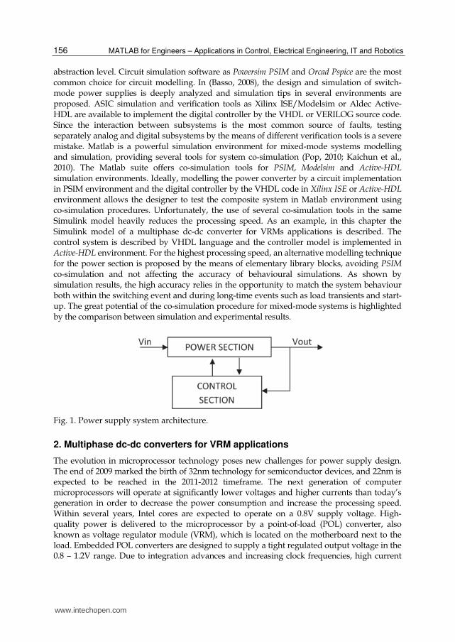
The inductor current never crosses zero during the switching period. A continuous conduction mode is preferred in high-current applications since lower and lower conduction power losses are involved. The capacitor current waveform is shown in Fig.4. When the capacitor current is positive, the stored charge as well as the capacitor voltage will increase. Vice versa, when the capacitor current goes negative, stored charge will be released and the output voltage will decrease as well. The total voltage change occurs between two consecutive zero-crossings of the capacitor current. Evaluating the total charge q as the grey-coloured area in Fig.4 yields:
圏 = なに∆荊挑に 劇に (7)
www.intechopen.com
MATLAB Co-Simulation Tools for Power Supply Systems Design 159
Fig. 4. At the top, the output capacitor current. At the bottom, the output voltage.
The voltage ripple across the output capacitor is given by:
∆撃 = 圏系 = ∆荊挑劇8系 (8)
Increasing the output capacitor value or the switching frequency directly improves the output voltage regulation. If a larger inductor is selected, the ripple current would decrease as well as the output voltage ripple. Yet, by increasing the inductor value the load transient response is worsened. A load transient could be modelled by the equivalent circuit shown in Fig.5.
Fig. 5. The equivalent circuit under large-signal load transients.
The load transient is modelled as an ideal current step. Since the input voltage is assumed constant, the switching node is dynamically tied to ground. The inductor is thus parallel connected to the output capacitor filter. If the loop response is sluggish, the peak output voltage deviation ∆撃墜通痛,陳銚掴 tends to approach the open-loop value which is given by:
∆撃墜通痛,陳銚掴 = ∆荊 ∙ 俵詣系 + 迎潔 ∙ ∆荊 (9)
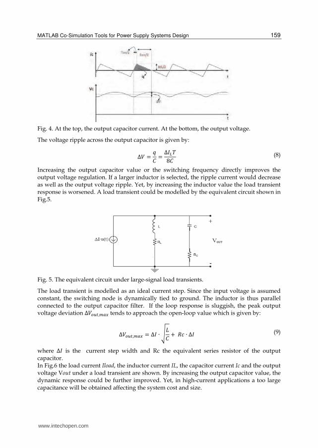
where ∆荊 is the current step width and Rc the equivalent series resistor of the output capacitor. In Fig.6 the load current Iload, the inductor current IL, the capacitor current Ic and the output voltage Vout under a load transient are shown. By increasing the output capacitor value, the dynamic response could be further improved. Yet, in high-current applications a too large capacitance will be obtained affecting the system cost and size.
www.intechopen.com
MATLAB for Engineers – Applications in Control, Electrical Engineering, IT and Robotics 160
Fig. 6. The converter waveforms under a large-signal transient.
The optimization of steady-state and dynamic performances leads to a trade-off in the choice of the inductor value. As will be further discussed, the inductor value is usually chosen to meet steady-state requirements and dynamic performances are improved by the control algorithm. As shown by (4), the buck converter reduces the dc input voltage by the means of switching elements. Power loss due to switches is ideally zero. Yet, switches are not ideal. Further, switching losses cannot be neglected. The inductor current flows through the MOSFET during the on-time and through the diode during the OFF time. Conduction losses are proportional to the forward voltage drop across the active elements. The MOSFET forward voltage drop is lower than the diode threshold voltage. In a buck converter, conduction losses are mainly due to the freewheeling diode. In high-current low-voltage applications, synchronous rectification is widely used to improve efficiency. As shown in Fig.7, the diode D is replaced by a MOSFET featuring a very low forward voltage drop. The rectification function, typically performed by diodes, is now achieved by the means of a MOSFET which is driven synchronously with the high-side MOSFET. For this reason, the added MOSFET is sometimes referred to as the synchronous rectifier MOSFET. Since the rectifier MOSFET source terminal is tied to the low-side of the input voltage rail, the MOSFET is also called low-side MOSFET. If compared with classical topology, synchronous rectification heavily reduces conduction losses improving efficiency. During the conduction time of the high-side (on time) the low-side is off and vice versa.
www.intechopen.com
MATLAB Co-Simulation Tools for Power Supply Systems Design 161
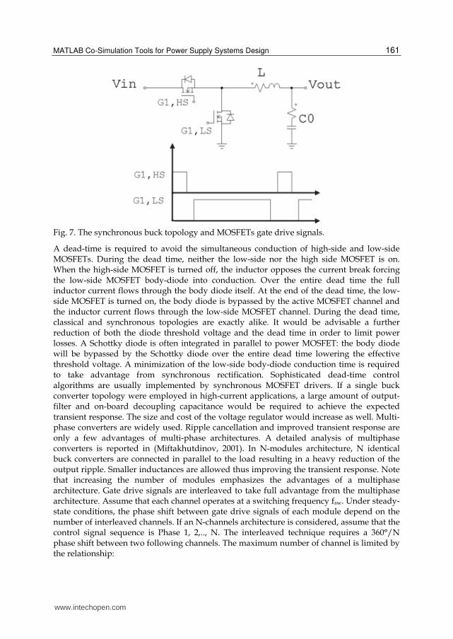
Fig. 7. The synchronous buck topology and MOSFETs gate drive signals.
A dead-time is required to avoid the simultaneous conduction of high-side and low-side MOSFETs. During the dead time, neither the low-side nor the high side MOSFET is on. When the high-side MOSFET is turned off, the inductor opposes the current break forcing the low-side MOSFET body-diode into conduction. Over the entire dead time the full inductor current flows through the body diode itself. At the end of the dead time, the low-side MOSFET is turned on, the body diode is bypassed by the active MOSFET channel and the inductor current flows through the low-side MOSFET channel. During the dead time, classical and synchronous topologies are exactly alike. It would be advisable a further reduction of both the diode threshold voltage and the dead time in order to limit power losses. A Schottky diode is often integrated in parallel to power MOSFET: the body diode will be bypassed by the Schottky diode over the entire dead time lowering the effective threshold voltage. A minimization of the low-side body-diode conduction time is required to take advantage from synchronous rectification. Sophisticated dead-time control algorithms are usually implemented by synchronous MOSFET drivers. If a single buck converter topology were employed in high-current applications, a large amount of output-filter and on-board decoupling capacitance would be required to achieve the expected transient response. The size and cost of the voltage regulator would increase as well. Multi-phase converters are widely used. Ripple cancellation and improved transient response are only a few advantages of multi-phase architectures. A detailed analysis of multiphase converters is reported in (Miftakhutdinov, 2001). In N-modules architecture, N identical buck converters are connected in parallel to the load resulting in a heavy reduction of the output ripple. Smaller inductances are allowed thus improving the transient response. Note that increasing the number of modules emphasizes the advantages of a multiphase architecture. Gate drive signals are interleaved to take full advantage from the multiphase architecture. Assume that each channel operates at a switching frequency fsw. Under steady-state conditions, the phase shift between gate drive signals of each module depend on the number of interleaved channels. If an N-channels architecture is considered, assume that the control signal sequence is Phase 1, 2,.., N. The interleaved technique requires a 360°/N phase shift between two following channels. The maximum number of channel is limited by the relationship:
www.intechopen.com
MATLAB for Engineers – Applications in Control, Electrical Engineering, IT and Robotics 162
岫な − 経岻 伴 軽 ∙ 経 (10)
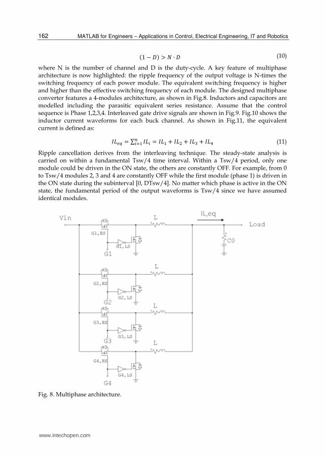
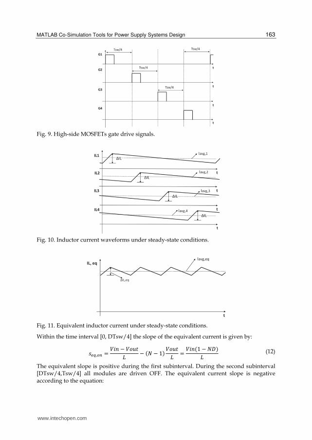
where N is the number of channel and D is the duty-cycle. A key feature of multiphase architecture is now highlighted: the ripple frequency of the output voltage is N-times the switching frequency of each power module. The equivalent switching frequency is higher and higher than the effective switching frequency of each module. The designed multiphase converter features a 4-modules architecture, as shown in Fig.8. Inductors and capacitors are modelled including the parasitic equivalent series resistance. Assume that the control sequence is Phase 1,2,3,4. Interleaved gate drive signals are shown in Fig.9. Fig.10 shows the inductor current waveforms for each buck channel. As shown in Fig.11, the equivalent current is defined as:
荊詣勅槌 = ∑ 荊詣沈津沈退怠 = 荊詣怠 + 荊詣態 + 荊詣戴 + 荊詣替 (11)
Ripple cancellation derives from the interleaving technique. The steady-state analysis is carried on within a fundamental Tsw/4 time interval. Within a Tsw/4 period, only one module could be driven in the ON state, the others are constantly OFF. For example, from 0 to Tsw/4 modules 2, 3 and 4 are constantly OFF while the first module (phase 1) is driven in the ON state during the subinterval [0, DTsw/4]. No matter which phase is active in the ON state, the fundamental period of the output waveforms is Tsw/4 since we have assumed identical modules.
Fig. 8. Multiphase architecture.
www.intechopen.com
MATLAB Co-Simulation Tools for Power Supply Systems Design 163
Fig. 9. High-side MOSFETs gate drive signals.
Fig. 10. Inductor current waveforms under steady-state conditions.
Fig. 11. Equivalent inductor current under steady-state conditions.
Within the time interval [0, DTsw/4] the slope of the equivalent current is given by:
嫌勅槌,墜津 = 撃件券 − 撃剣憲建詣 − 岫軽 − な岻撃剣憲建詣 = 撃件券岫な − 軽経岻詣 (12)
The equivalent slope is positive during the first subinterval. During the second subinterval [DTsw/4,Tsw/4] all modules are driven OFF. The equivalent current slope is negative according to the equation:
www.intechopen.com
MATLAB for Engineers – Applications in Control, Electrical Engineering, IT and Robotics 164
嫌勅槌,墜捗捗 = −軽撃剣憲建詣 (13)
The equivalent current ripple is given by:
∆荊挑,勅槌 = 撃件券岫な − 軽経岻経詣 劇鎚栂 = ∆荊詣 岫な − 軽経岻岫な − 経岻 (14)
As (14) states, in a multiphase architecture the current ripple is cancelled. If compared with classical buck converters, the current ripple is reduced by (1-ND)/(1-D). Moreover, the equivalent switching frequency as seen by the power load is N times the operating switching frequency of each power module. Note that (14) could be expressed as:
∆荊挑,勅槌 = 撃件券岫な − 軽経岻経詣 劇鎚栂 = 撃件券岫な − 軽経岻経軽 ∙ 軽軽 ∙ 軽 詣 劇鎚栂 = 撃件券, 結圏岫な − 経結圏岻経結圏詣結圏 劇鎚栂,勅槌 (15)
where N is the number of modules and 経結圏 = 軽 ∙ 経, 血嫌拳, 結圏 = 軽 ∙ 血嫌拳, 詣結圏 = 挑朝 , 撃件券, 結圏 =蝶沈津朝 . By comparing (15) and (5), conclusions are drawn: a N-modules architecture is equivalent to a buck converter operating at fsw,eq switching frequency, Deq duty-cycle, supplied by Vin,eq
input voltage and featuring Leq inductance. Then, if compared with a buck converter fed by the same input voltage rail and supplying the same voltage bus, the multiphase architecture features higher switching frequency, higher duty-cycle and lower inductance. Both steady-state and dynamic performances of the switching regulator take a great advantage from these interesting properties. With regards to steady-state performances, tight voltage regulation could be achieved thanks to the ripple cancellation effect. Dynamic performances are greatly improved by the reduction of the equivalent inductor under load transients. The steady-state and dynamic performances of multiphase converters are affected by the duty cycle value. A narrow duty cycle results in a poor ripple cancellation. Hence, a larger inductance should be selected to keep tight voltage regulation worsening the transient response. If a wide input-output voltage range is considered, a proper design of passive components is not yet suitable for speeding up the system performances. Multiphase architectures achieving a duty cycle extension by the means of coupled inductors are frequently proposed in literature. Otherwise, unconventional control algorithms are proposed to speed up the transient response not affecting the passive components design.
3. The control system
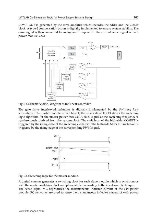
A survey of the control algorithm is given to highlight the system complexity and high accuracy of simulation results. Authors suggest (Boscaino et al., 2009) for further details. A linear-non-linear digital controller oriented to IC implementation, improving both steady-state and transient response is presented. A schematic block diagram of the linear loop is shown in Fig.12. A Pulse Width Modulation (PWM) current-mode control is implemented. Two 10 bits/2V ADCs and a 12 bits /5V DAC are included in the analog-digital interface. The output voltage is converted to digital and compared to a reference voltage Vref. The error signal
www.intechopen.com
MATLAB Co-Simulation Tools for Power Supply Systems Design 165
COMP_OUT is generated by the error amplifier which includes the adder and the COMP block. A type-2 compensation action is digitally implemented to ensure system stability. The error signal is then converted to analog and compared to the current sense signal of each power module Vc2,i.
Fig. 12. Schematic block diagram of the linear controller.
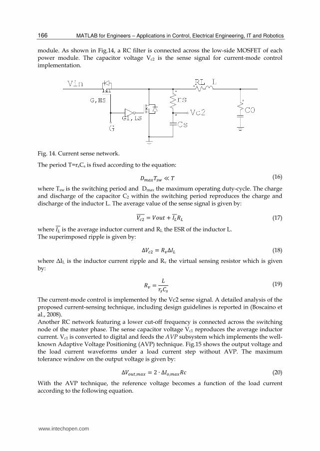
The gate drive interleaved technique is digitally implemented by the Switching logic subsystems. The master module is the Phase 1, the others slave. Fig.13 shows the switching logic algorithm for the master power module. A clock signal at the switching frequency is synchronously derived from the system clock. The switch-on of the high-side MOSFET is triggered by the rising-edge of the switching clock Ck1. The high-side MOSFET switch-off is triggered by the rising-edge of the corresponding PWM signal.
Fig. 13. Switching logic for the master module.
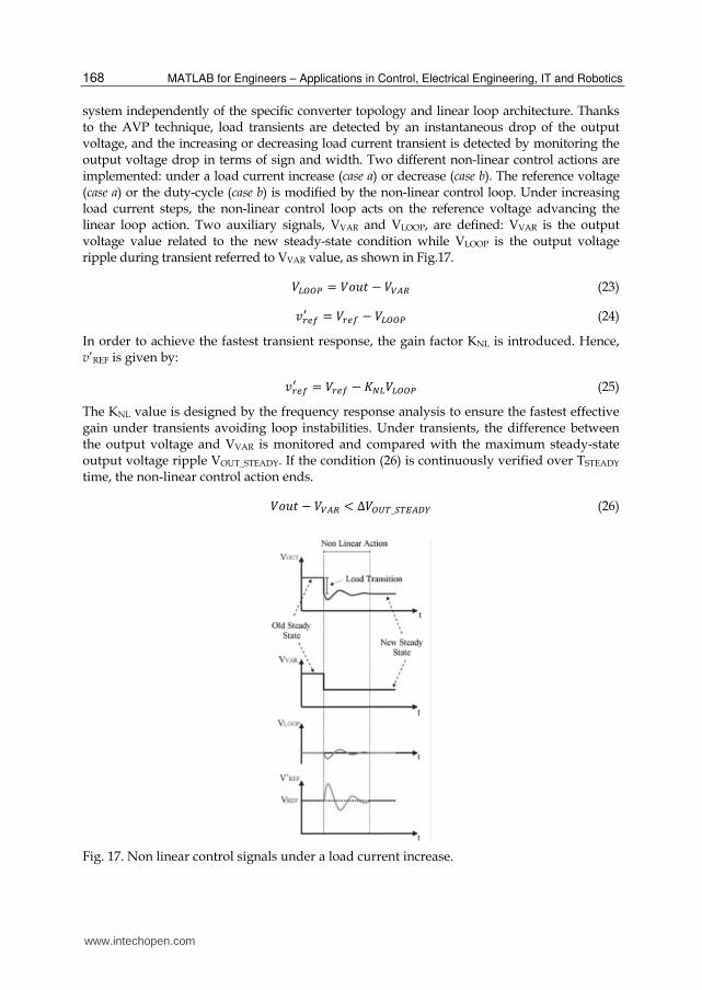
A digital counter generates a switching clock for each slave module which is synchronous with the master switching clock and phase-shifted according to the interleaved technique. The sense signal Vc2,i reproduces the instantaneous inductor current of the i-th power module. RC networks are used to sense the instantaneous inductor current of each power
www.intechopen.com
MATLAB for Engineers – Applications in Control, Electrical Engineering, IT and Robotics 166
module. As shown in Fig.14, a RC filter is connected across the low-side MOSFET of each power module. The capacitor voltage Vc2 is the sense signal for current-mode control implementation.
Fig. 14. Current sense network.
The period T=rsCs is fixed according to the equation: 経陳銚掴劇鎚栂 ≪ 劇 (16)
where Tsw is the switching period and Dmax the maximum operating duty-cycle. The charge and discharge of the capacitor C2 within the switching period reproduces the charge and discharge of the inductor L. The average value of the sense signal is given by:
撃頂態 = 撃剣憲建 + 荊挑迎挑 (17)
where 荊挑 is the average inductor current and RL the ESR of the inductor L. The superimposed ripple is given by:
∆撃頂態 = 迎塚∆荊挑 (18)
where ΔIL is the inductor current ripple and Rv the virtual sensing resistor which is given by:
迎塚 = 詣堅鎚系鎚 (19)
The current-mode control is implemented by the Vc2 sense signal. A detailed analysis of the proposed current-sensing technique, including design guidelines is reported in (Boscaino et al., 2008). Another RC network featuring a lower cut-off frequency is connected across the switching node of the master phase. The sense capacitor voltage Vc1 reproduces the average inductor current. Vc1 is converted to digital and feeds the AVP subsystem which implements the well-known Adaptive Voltage Positioning (AVP) technique. Fig.15 shows the output voltage and the load current waveforms under a load current step without AVP. The maximum tolerance window on the output voltage is given by:
∆撃墜通痛,陳銚掴 = に ∙ ∆荊墜,陳銚掴迎潔 (20)
With the AVP technique, the reference voltage becomes a function of the load current according to the following equation.
www.intechopen.com

MATLAB Co-Simulation Tools for Power Supply Systems Design 167
Fig. 15. Dynamic response under load transients. At the top the load current step, at the bottom, the output voltage waveforms are shown.
懸追勅捗嫗 = 撃追勅捗 − 荊墜迎潔 (21)
where, v’ref is the variable reference voltage, Vref is a fixed reference voltage, Io is the load current and Rc is the equivalent series resistor of the output capacitor. The DC set point of the output voltage changes accordingly to the output current, as shown in Fig.16. At steady-state, the output voltage is forced by the AVP technique to the variable reference voltage, instead of a fixed value Vref . Under high-load conditions, the DC set point drops in the lower part of the allowable tolerance window. The maximum tolerance window is now given by:
∆撃墜通痛,陳銚掴 = ∆荊墜,陳銚掴迎潔 (22)
The technique results in added margin to handle load transients. Since the load current is equal to the average inductor current, the AVP technique is implemented by sensing the average inductor current of the master phase.
Fig. 16. The dynamic response to a load current step with Adaptive Voltage Positioning.
A non-linear control is introduced to speed-up the transient response not affecting steady-state performances. During transients, the non-linear control modifies a few linear loop parameters, as the reference voltage or the duty-cycle. Since the converter output voltage is the only non-linear loop input, the proposed technique can be efficiently applied to each power supply
www.intechopen.com
MATLAB for Engineers – Applications in Control, Electrical Engineering, IT and Robotics 168
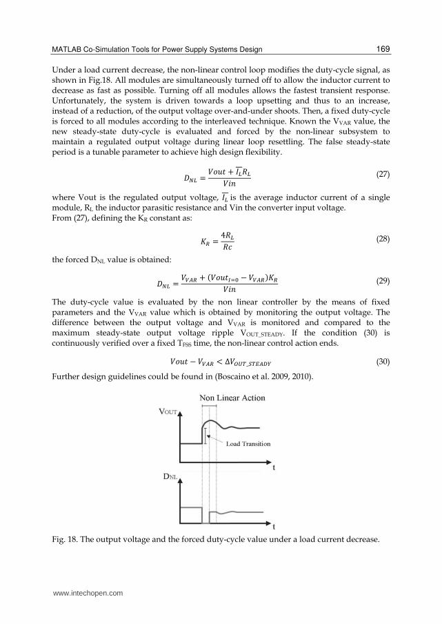
system independently of the specific converter topology and linear loop architecture. Thanks to the AVP technique, load transients are detected by an instantaneous drop of the output voltage, and the increasing or decreasing load current transient is detected by monitoring the output voltage drop in terms of sign and width. Two different non-linear control actions are implemented: under a load current increase (case a) or decrease (case b). The reference voltage (case a) or the duty-cycle (case b) is modified by the non-linear control loop. Under increasing load current steps, the non-linear control loop acts on the reference voltage advancing the linear loop action. Two auxiliary signals, VVAR and VLOOP, are defined: VVAR is the output voltage value related to the new steady-state condition while VLOOP is the output voltage ripple during transient referred to VVAR value, as shown in Fig.17.
撃挑潮潮牒 = 撃剣憲建 − 撃蝶凋眺 (23)
懸追勅捗嫗 = 撃追勅捗 − 撃挑潮潮牒 (24)
In order to achieve the fastest transient response, the gain factor KNL is introduced. Hence, v’REF is given by:
懸追勅捗嫗 = 撃追勅捗 − 計朝挑撃挑潮潮牒 (25)
The KNL value is designed by the frequency response analysis to ensure the fastest effective gain under transients avoiding loop instabilities. Under transients, the difference between the output voltage and VVAR is monitored and compared with the maximum steady-state output voltage ripple VOUT_STEADY. If the condition (26) is continuously verified over TSTEADY time, the non-linear control action ends.
撃剣憲建 − 撃蝶凋眺 < ∆撃潮腸脹_聴脹帳凋帖超 (26)
Fig. 17. Non linear control signals under a load current increase.
www.intechopen.com
MATLAB Co-Simulation Tools for Power Supply Systems Design 169
Under a load current decrease, the non-linear control loop modifies the duty-cycle signal, as shown in Fig.18. All modules are simultaneously turned off to allow the inductor current to decrease as fast as possible. Turning off all modules allows the fastest transient response. Unfortunately, the system is driven towards a loop upsetting and thus to an increase, instead of a reduction, of the output voltage over-and-under shoots. Then, a fixed duty-cycle is forced to all modules according to the interleaved technique. Known the VVAR value, the new steady-state duty-cycle is evaluated and forced by the non-linear subsystem to maintain a regulated output voltage during linear loop resettling. The false steady-state period is a tunable parameter to achieve high design flexibility.
経朝挑 = 撃剣憲建 + 荊挑迎挑撃件券 (27)
where Vout is the regulated output voltage, 荊挑is the average inductor current of a single module, RL the inductor parasitic resistance and Vin the converter input voltage. From (27), defining the KR constant as:
計眺 = 4迎挑迎潔 (28)
the forced DNL value is obtained:
経朝挑 = 撃蝶凋眺 + 岫撃剣憲建彫退待 − 撃蝶凋眺岻計眺撃件券 (29)
The duty-cycle value is evaluated by the non linear controller by the means of fixed parameters and the VVAR value which is obtained by monitoring the output voltage. The difference between the output voltage and VVAR is monitored and compared to the maximum steady-state output voltage ripple VOUT_STEADY. If the condition (30) is continuously verified over a fixed TFSS time, the non-linear control action ends.
撃剣憲建 − 撃蝶凋眺 < ∆撃潮腸脹_聴脹帳凋帖超 (30)
Further design guidelines could be found in (Boscaino et al. 2009, 2010).
Fig. 18. The output voltage and the forced duty-cycle value under a load current decrease.
www.intechopen.com

MATLAB for Engineers – Applications in Control, Electrical Engineering, IT and Robotics 170
4. Co-simulation set-up
Active-HDL provides an interface to MATLAB/Simulink simulation environment which allows co-simulation of functional blocks described by using hardware description languages. The digital controller is tested on a FPGA device. A specific co-simulation procedure should be activated in order to make each VHDL design unit available in Simulink libraries. The VHDL code and signal timing are tested as well. High-accuracy simulation results are obtained heavily reducing experimental fault conditions. The co-simulation procedure features automatic data type conversion between Simulink and Active HDL and simulation results could be displayed in both simulation environments. All VHDL entities are collected in an Active HDL workspace. A MATLAB m-file is generated for each VHDL entity. By right clicking on a VHDL entity, select the option “Generate Block Description for Simulink”. The procedure is repeated for each VHDL entity of current Workspace. After generating the m-files, the Active-HDL Blockset is available in the Simulink library browser. The Active-HDL Co-Sim and HDL Black-Box elements are used for system co-simulation. The Active-HDL Co-Sim element must be included in the Simulink top level model. The block allows the designer to fix co-simulation parameters. In order to simulate a VHDL entity as an integral part of the current model, a HDL Black-Box block should be added and associated to the corresponding m-file by the configuration box. When the model is completed, running simulation from Simulink starts the co-simulation. The connection to the Active-HDL server will be opened and all HDL Black-Boxes simulated with the Active-HDL simulator. Input and output waveforms can be analyzed both in Simulink and Aldec environment while internal signal waveforms can be analyzed in Aldec environment only.
5. MATLAB/Simulink model
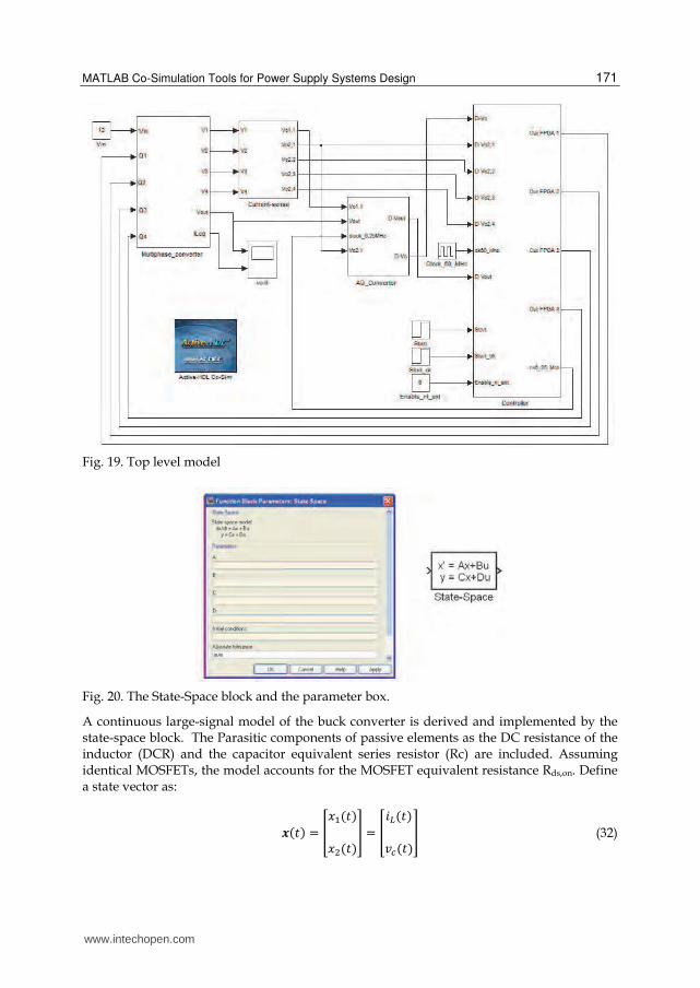
The top level model is shown in Fig.19. The power section includes the Multiphase converter and the Current-sense subsystems. In the A/D converter subsystem, the Analog-to-Digital interface is modelled by Simulink library elements. The controller is modelled in Aldec Active-HDL environment and each design unit is included in the Controller subsystem. The Active-HDL Co-Sim block is added to the top level model.
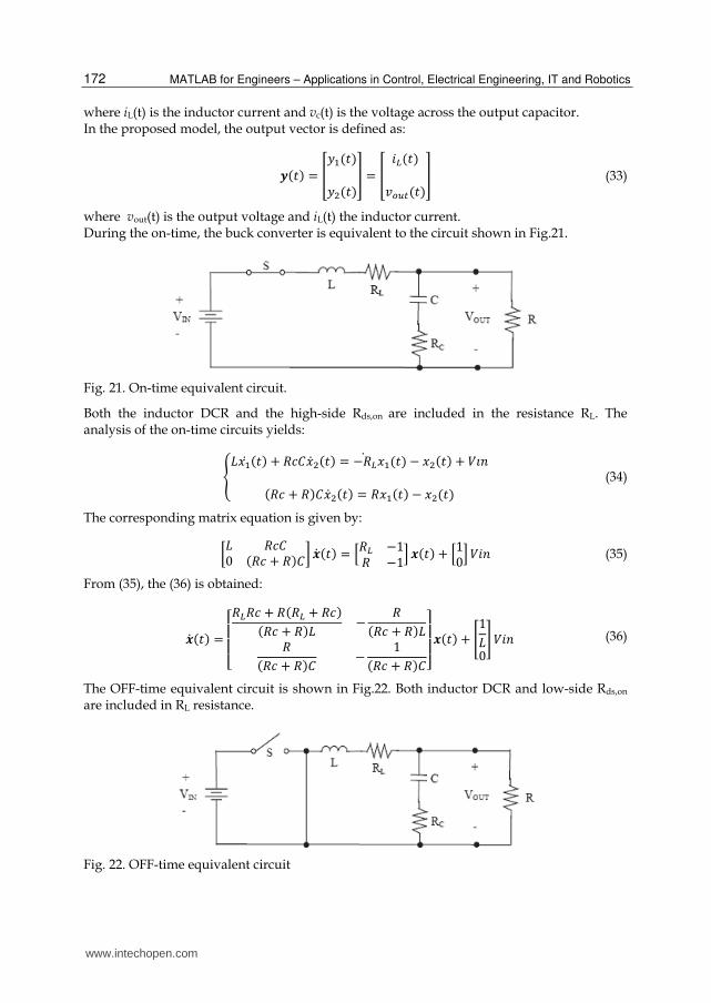
5.1 The power section model The power section includes the multiphase converter and current-sense filters. A four-module interleaved synchronous buck converter is connected to the power load. The power section is modelled by Simulink library elements in order to achieve the highest processing speed. The use of several co-simulation tools is avoided, keeping at the same time the highest accuracy. In this paragraph, the Simulink model of the multiphase converter based on a continuous-time large-signal model is described. The proposed modelling technique could be efficiently extended to each switching converter. In Simulink environment, the State-Space block models a system by its own state-space equations:
姉岌 = 冊姉 + 刷四
姿 = 察姉 + 拶四 (31)
where x is the state vector, u the input vector and y the output vector. According to (31), the block is fed by the input vector u and the output vector y is generated. As shown in Fig.20, the designer could enter the matrix coefficients in the parameter box.
www.intechopen.com
MATLAB Co-Simulation Tools for Power Supply Systems Design 171
Fig. 19. Top level model
Fig. 20. The State-Space block and the parameter box.
A continuous large-signal model of the buck converter is derived and implemented by the state-space block. The Parasitic components of passive elements as the DC resistance of the inductor (DCR) and the capacitor equivalent series resistor (Rc) are included. Assuming identical MOSFETs, the model accounts for the MOSFET equivalent resistance Rds,on. Define a state vector as:
姉岫建岻 = 崛捲怠岫建岻捲態岫建岻崑 = 崛件挑岫建岻懸頂岫建岻崑 (32)
www.intechopen.com
MATLAB for Engineers – Applications in Control, Electrical Engineering, IT and Robotics 172
where iL(t) is the inductor current and vc(t) is the voltage across the output capacitor. In the proposed model, the output vector is defined as:
姿岫建岻 = 崛検怠岫建岻検態岫建岻崑 = 崛 件挑岫建岻懸墜通痛岫建岻崑 (33)
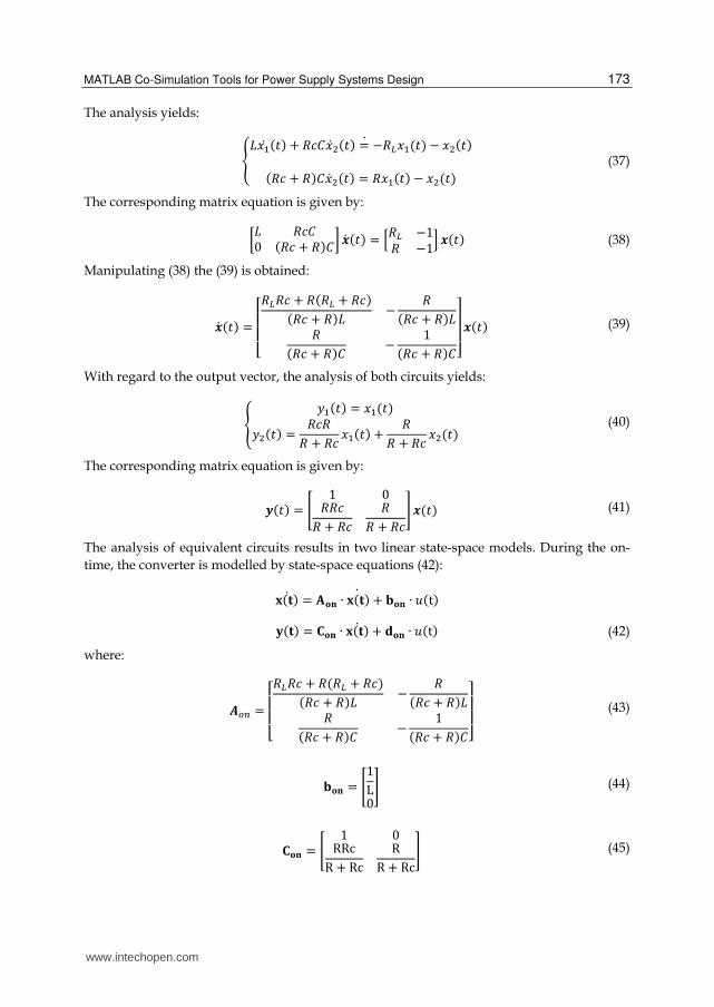
where vout(t) is the output voltage and iL(t) the inductor current. During the on-time, the buck converter is equivalent to the circuit shown in Fig.21.
Fig. 21. On-time equivalent circuit.
Both the inductor DCR and the high-side Rds,on are included in the resistance RL. The analysis of the on-time circuits yields:
崔詣捲怠岌 岫建岻 + 迎潔系捲岌態岫建岻 = −迎挑捲怠岫建岻 − 捲態岫建岻 + 撃続券岌岫迎潔 + 迎岻系捲岌態岫建岻 = 迎捲怠岫建岻 − 捲態岫建岻 (34)
The corresponding matrix equation is given by:
釆詣 迎潔系ど 岫迎潔 + 迎岻系挽 姉岌 岫建岻 = 峙迎挑 −な迎 −な峩 姉岫建岻 + 峙など峩撃件券 (35)
From (35), the (36) is obtained:
姉岌 岫建岻 = 琴欽欽欣迎挑迎潔 + 迎岫迎挑 + 迎潔岻岫迎潔 + 迎岻詣 − 迎岫迎潔 + 迎岻詣迎岫迎潔 + 迎岻系 − な岫迎潔 + 迎岻系筋禽禽
禁 姉岫建岻 + 煩な詣ど晩 撃件券 (36)
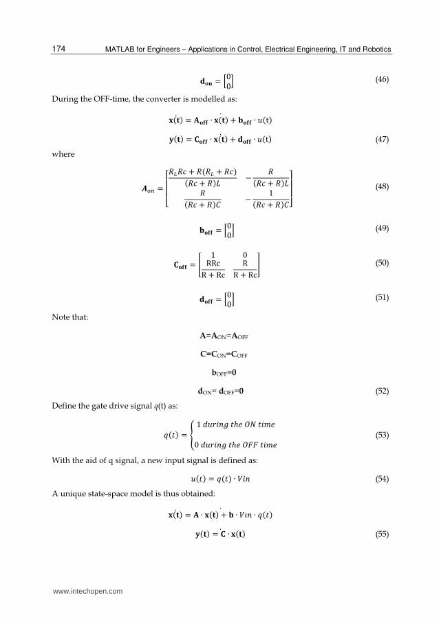
The OFF-time equivalent circuit is shown in Fig.22. Both inductor DCR and low-side Rds,on are included in RL resistance.
Fig. 22. OFF-time equivalent circuit
www.intechopen.com
MATLAB Co-Simulation Tools for Power Supply Systems Design 173
The analysis yields:
崔詣捲怠岌 岫建岻 + 迎潔系捲岌態岫建岻 = −迎挑捲怠岫建岻 − 捲態岫建岻岌岫迎潔 + 迎岻系捲岌態岫建岻 = 迎捲怠岫建岻 − 捲態岫建岻 (37)
The corresponding matrix equation is given by:
釆詣 迎潔系ど 岫迎潔 + 迎岻系挽 姉岌 岫建岻 = 峙迎挑 −な迎 −な峩 姉岫建岻 (38)
Manipulating (38) the (39) is obtained:
姉岌 岫建岻 = 琴欽欽欣迎挑迎潔 + 迎岫迎挑 + 迎潔岻岫迎潔 + 迎岻詣 − 迎岫迎潔 + 迎岻詣迎岫迎潔 + 迎岻系 − な岫迎潔 + 迎岻系筋禽禽
禁 姉岫建岻 (39)
With regard to the output vector, the analysis of both circuits yields:
崔 検怠岫建岻 = 捲怠岫建岻検態岫建岻 = 迎潔迎迎 + 迎潔 捲怠岫建岻 + 迎迎 + 迎潔 捲態岫建岻 (40)
The corresponding matrix equation is given by:
姿岫建岻 = 煩 な ど迎迎潔迎 + 迎潔 迎迎 + 迎潔晩 姉岫建岻 (41)
The analysis of equivalent circuits results in two linear state-space models. During the on-
time, the converter is modelled by state-space equations (42):
景岫憩岻岌 = 寓形契 ∙ 景岫憩岻 + 郡形契 ∙ 憲岫t岻岌
桂岫憩岻 = 隅形契 ∙ 景岫憩岻 + 袈形契 ∙ 憲岫t岻岌 (42)
where:
冊墜津 = 琴欽欽欣迎挑迎潔 + 迎岫迎挑 + 迎潔岻岫迎潔 + 迎岻詣 − 迎岫迎潔 + 迎岻詣迎岫迎潔 + 迎岻系 − な岫迎潔 + 迎岻系筋禽禽
禁 (43)
郡形契 = 煩なLど晩 (44)
隅形契 = 煩 な どRRcR + Rc RR + Rc晩 (45)
www.intechopen.com
MATLAB for Engineers – Applications in Control, Electrical Engineering, IT and Robotics 174
袈形契 = 峙どど峩 (46)
During the OFF-time, the converter is modelled as:
景岫憩岻岌 = 寓形係係 ∙ 景岫憩岻 + 郡形係係 ∙ 憲岫t岻岌
桂岫憩岻 = 隅形係係 ∙ 景岫憩岻 + 袈形係係 ∙ 憲岫t岻岌 (47)
where
冊墜津 = 琴欽欽欣迎挑迎潔 + 迎岫迎挑 + 迎潔岻岫迎潔 + 迎岻詣 − 迎岫迎潔 + 迎岻詣迎岫迎潔 + 迎岻系 − な岫迎潔 + 迎岻系筋禽禽
禁 (48)
郡形係係 = 峙どど峩 (49)
隅形係係 = 煩 な どRRcR + Rc RR + Rc晩 (50)
袈形係係 = 峙どど峩 (51)
Note that:
A=AON=AOFF
C=CON=COFF
bOFF=0
dON= dOFF=0 (52)
Define the gate drive signal q(t) as:
圏岫建岻 = 崔 な穴憲堅件券訣建ℎ結頚軽建件兼結ど穴憲堅件券訣建ℎ結頚繋繋建件兼結 (53)
With the aid of q signal, a new input signal is defined as:
憲岫建岻 = 圏岫建岻 ∙ 撃件券 (54)
A unique state-space model is thus obtained:
景岫憩岻岌 = 寓 ∙ 景岫憩岻 + 郡 ∙ 撃続券 ∙ 圏岫建岻岌
桂岫憩岻 = 隅 ∙ 景岫憩岻岌 (55)
www.intechopen.com
MATLAB Co-Simulation Tools for Power Supply Systems Design 175
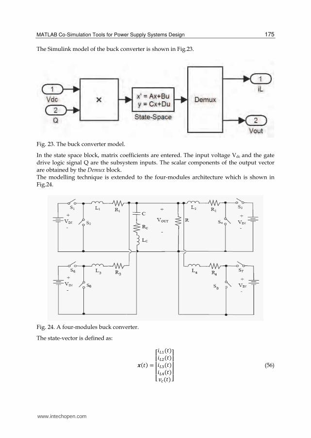
The Simulink model of the buck converter is shown in Fig.23.
Fig. 23. The buck converter model.
In the state space block, matrix coefficients are entered. The input voltage Vdc and the gate
drive logic signal Q are the subsystem inputs. The scalar components of the output vector
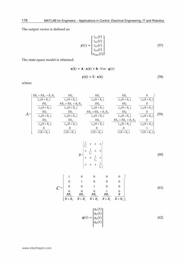
are obtained by the Demux block. The modelling technique is extended to the four-modules architecture which is shown in Fig.24.
Fig. 24. A four-modules buck converter.
The state-vector is defined as:
姉岫建岻 = 琴欽欽欽欣件挑怠岫建岻件挑態岫建岻件挑戴岫建岻件挑替岫建岻懸頂岫建岻 筋禽禽
禽禁 (56)
www.intechopen.com
MATLAB for Engineers – Applications in Control, Electrical Engineering, IT and Robotics 176
The output vector is defined as:
姿岫建岻 = 琴欽欽欽欣 件挑怠岫建岻件挑態岫建岻件挑戴岫建岻件挑替岫建岻懸墜通痛岫建岻筋禽禽
禽禁 (57)
The state-space model is obtained:
景岫憩岻岌 = 寓 ∙ 景岫憩岻 + 郡 ∙ 撃続券 ∙ 刺岫建岻岌
桂岫憩岻 = 隅 ∙ 景岫憩岻岌 (58)
where:
1 1
1 1 1 1 1
2 2
2 2 2 2 2
3 3
3 3 3 3 3
( ) ( ) ( ) ( ) ( )
( ) ( ) ( ) ( ) ( )
( ) ( ) ( ) ( ) (
C C C C C
C C C C C
C C C C C
C C C C C
C C C C C
C C C C
RR RR R R RR RR RR R
L R R L R R L R R L R R L R R
RR RR RR R R RR RR R
L R R L R R L R R L R R L R R
RR RR RR RR R R RR R
L R R L R R L R R L R R L R RA
+ +− − − −
+ + + + +
+ +− − − − −
+ + + + +
+ +− − − − −=
+ + + + +
4 4
4 4 4 4 4
)
( ) ( ) ( ) ( ) ( )
1
( ) ( ) ( ) ( ) ( )
C
C C C C C
C C C C C
C C C C C
RR RR RR RR RR R R R
L R R L R R L R R L R R L R R
R R R R
C R R C R R C R R C R R C R R
+ +− − − − −
+ + + + + −
+ + + + +
(59)
1
2
3
4
10 0 0
10 0 0
10 0 0
10 0 0
L
L
L
L
B
=
(60)
+++++
=
CC
C
C
C
C
C
C
C
RR
R
RR
RR
RR
RR
RR
RR
RR
RR
C01000
00100
00010
00001
(61)
刺岫建岻 = 琴欽欽欽欣圏怠岫建岻圏態岫建岻圏戴岫建岻圏替岫建岻筋禽禽
禽禁 (62)
www.intechopen.com
MATLAB Co-Simulation Tools for Power Supply Systems Design 177
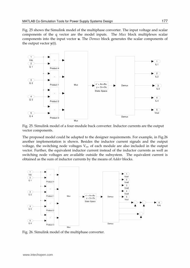
Fig. 25 shows the Simulink model of the multiphase converter. The input voltage and scalar components of the q vector are the model inputs. The Mux block multiplexes scalar components into the input vector u. The Demux block generates the scalar components of the output vector y(t).
Fig. 25. Simulink model of a four-module buck converter. Inductor currents are the output vector components.
The proposed model could be adapted to the designer requirements. For example, in Fig.26 another implementation is shown. Besides the inductor current signals and the output voltage, the switching node voltages Vsw of each module are also included in the output vector. Further, the equivalent inductor current instead of the inductor currents as well as switching node voltages are available outside the subsystem. The equivalent current is obtained as the sum of inductor currents by the means of Adder blocks.
Fig. 26. Simulink model of the multiphase converter.
Vout
5
IL 4
4
IL3
3
IL 2
2
IL 1
1
State -Space
x' = Ax+Bu
y = Cx+Du
Product 4
Product 3
Product 2
Product 1
Mux
Mux
Demux
Demux
Q 4
5
Q 3
4
Q 2
3
Q 1
2
Vdc
1
ILeq
6
Vout
5
Vsw4
4
Vsw3
3
Vsw2
2
Vsw1
1
State -Space
x' = Ax+Bu
y = Cx+Du
Product 4
Product 3
Product 2
Product 1
Mux
Mux
Demux
Demux
Q 4
5
Q 3
4
Q 2
3
Q 1
2
Vdc
1
www.intechopen.com
MATLAB for Engineers – Applications in Control, Electrical Engineering, IT and Robotics 178
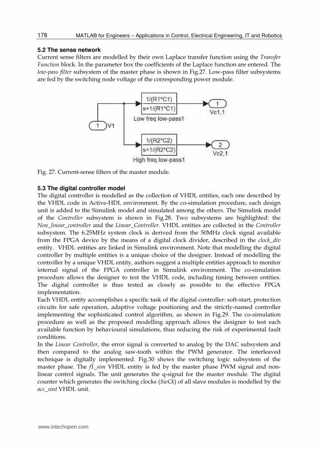
5.2 The sense network Current sense filters are modelled by their own Laplace transfer function using the Transfer Function block. In the parameter box the coefficients of the Laplace function are entered. The low-pass filter subsystem of the master phase is shown in Fig.27. Low-pass filter subsystems are fed by the switching node voltage of the corresponding power module.
Fig. 27. Current-sense filters of the master module.
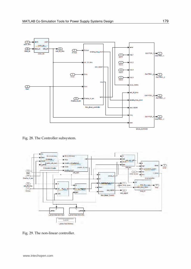
5.3 The digital controller model The digital controller is modelled as the collection of VHDL entities, each one described by the VHDL code in Active-HDL environment. By the co-simulation procedure, each design unit is added to the Simulink model and simulated among the others. The Simulink model of the Controller subsystem is shown in Fig.28. Two subsystems are highlighted: the Non_linear_controller and the Linear_Controller. VHDL entities are collected in the Controller subsystem. The 6.25MHz system clock is derived from the 50MHz clock signal available from the FPGA device by the means of a digital clock divider, described in the clock_div entity. VHDL entities are linked in Simulink environment. Note that modelling the digital controller by multiple entities is a unique choice of the designer. Instead of modelling the controller by a unique VHDL entity, authors suggest a multiple entities approach to monitor internal signal of the FPGA controller in Simulink environment. The co-simulation procedure allows the designer to test the VHDL code, including timing between entities. The digital controller is thus tested as closely as possible to the effective FPGA implementation. Each VHDL entity accomplishes a specific task of the digital controller: soft-start, protection circuits for safe operation, adaptive voltage positioning and the strictly-named controller implementing the sophisticated control algorithm, as shown in Fig.29. The co-simulation procedure as well as the proposed modelling approach allows the designer to test each available function by behavioural simulations, thus reducing the risk of experimental fault conditions. In the Linear Controller, the error signal is converted to analog by the DAC subsystem and then compared to the analog saw-tooth within the PWM generator. The interleaved technique is digitally implemented. Fig.30 shows the switching logic subsystem of the master phase. The f1_sim VHDL entity is fed by the master phase PWM signal and non-linear control signals. The unit generates the q-signal for the master module. The digital counter which generates the switching clocks (SwCk) of all slave modules is modelled by the acc_sint VHDL unit.
www.intechopen.com
MATLAB Co-Simulation Tools for Power Supply Systems Design 179
Fig. 28. The Controller subsystem.
Fig. 29. The non-linear controller.
www.intechopen.com
MATLAB for Engineers – Applications in Control, Electrical Engineering, IT and Robotics 180
Fig. 30. The Switching Logic model of the master module.
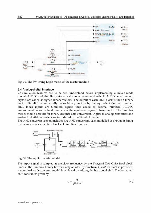
5.4 Analog-digital interface Co-simulation features are to be well-understood before implementing a mixed-mode model. ALDEC and Simulink automatically code common signals. In ALDEC environment signals are coded as signed binary vectors. The output of each HDL block is thus a binary vector. Simulink automatically codes binary vectors by the equivalent decimal number. HDL block inputs are Simulink signals thus coded as decimal numbers. ALDEC environment codes decimal numbers as the equivalent signed binary vector. The Simulink model should account for binary-decimal data conversion. Digital to analog converters and analog to digital converters are introduced in the Simulink model. The A/D converter section includes two A/D converters, each modelled as shown in Fig.31 by the means of elementary blocks of Simulink libraries.
Fig. 31. The A/D converter model
The input signal is sampled at the clock frequency by the Triggered Zero-Order Hold block. Since in the Simulink library browser only an ideal symmetrical Quantizer block is provided, a non-ideal A/D converter model is achieved by adding the horizontal shift. The horizontal shift constant is given by:
C = FSに択但辿担袋怠 (63)
www.intechopen.com
MATLAB Co-Simulation Tools for Power Supply Systems Design 181
where Nbit is the bit resolution and FS the full scale voltage. The available Quantizer block allows the user to set the voltage resolution while the number of levels is yet unlimited. The Saturation block is thus cascaded to the Quantizer in order to set the full scale range. The high-level saturation limit is given by:
High = V嘆奪坦 ∙ N狸奪旦 = FSに択但辿担 ∙ 岫に択但辿担 − な岻 (64)
where Vres is the voltage resolution and Nlev the number of levels. The discrete output of the Saturation block should be coded. In order to simulate the ADC coding, the Gain block is cascaded to the saturation block. The output of the ADC model is the equivalent decimal number of the binary vector. The conversion gain is given by:
K = FSに択但辿担 (65)
The Conversion Delay block accounts for the input-output delay of the modelled A/D converter. The Simulink model of the digital-to-analog converter is shown in Fig.32. The subsystem is fed by a digital signal and generates a discrete analog signal. The maximum value of the input signal is given by:
撃兼欠捲 = に朝弐日禰,匂尼迩 − な (66)
where Nbit,dac is the converter bit resolution. The maximum value of the output voltage is equal to the DAC full scale voltage. The digital-to-analog converter is modelled by a gain factor Kdac: K辰叩達 = FS辰叩達に択党套盗,凍倒冬 (67)
In order to model the full scale range of the converter, a Saturation block is cascaded with the gain block. Saturation levels are equal to the full scale range.
Fig. 32. The Simulink model of a digital-to-analog converter.
5.5 PWM comparator model The PWM comparator is fed by the analog error signal and the analog current sense signal. The analog comparator model is shown in Fig.33. An adder block is used as the input stage of the comparator. The Relay block models the non-linearity of the comparator. The Relay block allows its output to switch between two specified values. The state of the relay is obtained by comparing the input signal to the specified thresholds, the Switch-off point and the Switch-on point parameters. When the relay is on, it remains on until the input drops below the value of the Switch-off point parameter. When the relay is off, it remains off until the input exceeds the value of the Switch-on point parameter. The parameter box allows the
analog
1
SaturationDAC Gain
-K-
Conversion Delaydigital
1
www.intechopen.com

MATLAB for Engineers – Applications in Control, Electrical Engineering, IT and Robotics 182
end user to set a specified value for both on and off conditions. In this model, the output value is equal to “1” in the on-state, “0” in the off-state.
Fig. 33. The Simulink model of the PWM comparator.
6. Simulation results
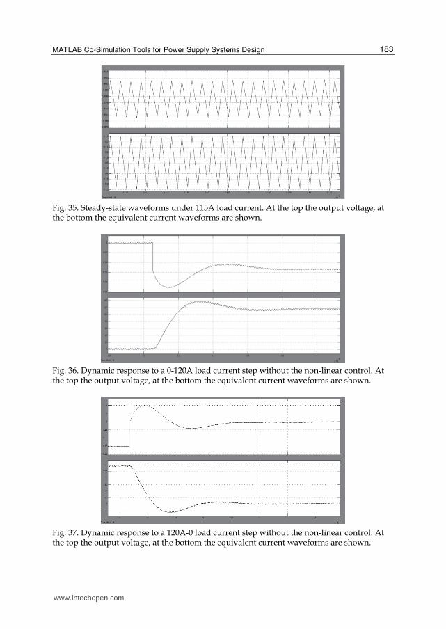
A 12V/1V@120A four-module buck converter has been designed and modelled in Simulink-Aldec mixed environment. Each power module operates at 250kHz switching frequency. Simulation results are shown to highlight the high accuracy of the modelling approach. Steady-state waveforms under 1A load are shown in Fig.34. At the top the output voltage waveform, at the bottom the equivalent inductor current is shown. The proposed modelling approach allows the designer to simulate the system behaviour within the switching period achieving high accuracy results. The output voltage ripple and the current ripple are accurately modelled. The DC set point of the output voltage is fixed at the nominal value. The output voltage, at the top, and the equivalent current, at the bottom, under 115A load are shown in Fig.35. The DC set point is fixed at 0.96V at full load due to the implemented AVP technique. The system is tested under load current transients to evaluate the non-linear control performances. Under a 0-120A load current step, if the non linear controller is disabled the system behaviour shown in Fig.36 is obtained. Under a 120A -0 load current step, if the non linear controller is disabled the system behaviour shown in Fig.37 is obtained. The output voltage, at the top, and the equivalent current, at the bottom, are shown. Note that the proposed design approach accurately models the system behaviour within the switching period as well as under large-signal transients.
Fig. 34. Steady-state waveforms under 1A load current. At the top the output voltage, at the bottom the equivalent current waveforms are shown.
Out 1
1
Relay 1
-
2
+
1
www.intechopen.com
MATLAB Co-Simulation Tools for Power Supply Systems Design 183
Fig. 35. Steady-state waveforms under 115A load current. At the top the output voltage, at the bottom the equivalent current waveforms are shown.
Fig. 36. Dynamic response to a 0-120A load current step without the non-linear control. At the top the output voltage, at the bottom the equivalent current waveforms are shown.
Fig. 37. Dynamic response to a 120A-0 load current step without the non-linear control. At the top the output voltage, at the bottom the equivalent current waveforms are shown.
www.intechopen.com
MATLAB for Engineers – Applications in Control, Electrical Engineering, IT and Robotics 184
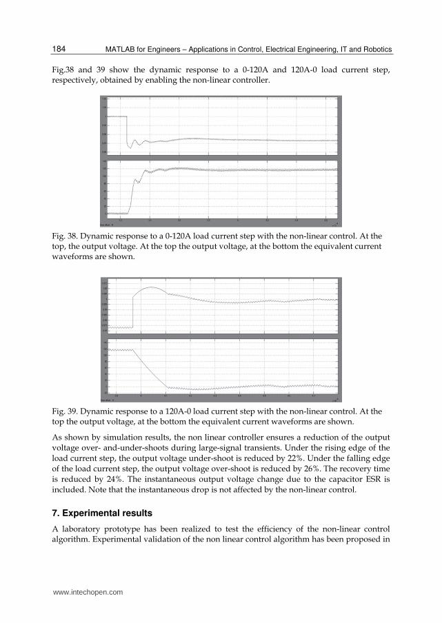
Fig.38 and 39 show the dynamic response to a 0-120A and 120A-0 load current step, respectively, obtained by enabling the non-linear controller.
Fig. 38. Dynamic response to a 0-120A load current step with the non-linear control. At the top, the output voltage. At the top the output voltage, at the bottom the equivalent current waveforms are shown.
Fig. 39. Dynamic response to a 120A-0 load current step with the non-linear control. At the top the output voltage, at the bottom the equivalent current waveforms are shown.
As shown by simulation results, the non linear controller ensures a reduction of the output
voltage over- and-under-shoots during large-signal transients. Under the rising edge of the
load current step, the output voltage under-shoot is reduced by 22%. Under the falling edge
of the load current step, the output voltage over-shoot is reduced by 26%. The recovery time
is reduced by 24%. The instantaneous output voltage change due to the capacitor ESR is
included. Note that the instantaneous drop is not affected by the non-linear control.
7. Experimental results
A laboratory prototype has been realized to test the efficiency of the non-linear control algorithm. Experimental validation of the non linear control algorithm has been proposed in
www.intechopen.com
MATLAB Co-Simulation Tools for Power Supply Systems Design 185
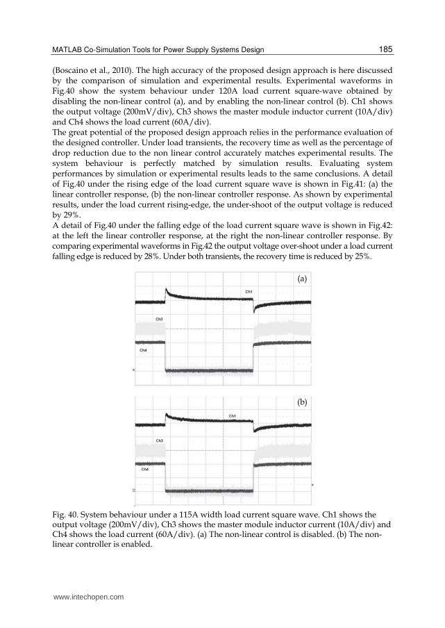
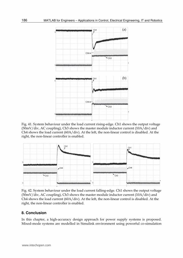
(Boscaino et al., 2010). The high accuracy of the proposed design approach is here discussed by the comparison of simulation and experimental results. Experimental waveforms in Fig.40 show the system behaviour under 120A load current square-wave obtained by disabling the non-linear control (a), and by enabling the non-linear control (b). Ch1 shows the output voltage (200mV/div), Ch3 shows the master module inductor current (10A/div) and Ch4 shows the load current (60A/div). The great potential of the proposed design approach relies in the performance evaluation of the designed controller. Under load transients, the recovery time as well as the percentage of drop reduction due to the non linear control accurately matches experimental results. The system behaviour is perfectly matched by simulation results. Evaluating system performances by simulation or experimental results leads to the same conclusions. A detail of Fig.40 under the rising edge of the load current square wave is shown in Fig.41: (a) the linear controller response, (b) the non-linear controller response. As shown by experimental results, under the load current rising-edge, the under-shoot of the output voltage is reduced by 29%. A detail of Fig.40 under the falling edge of the load current square wave is shown in Fig.42: at the left the linear controller response, at the right the non-linear controller response. By comparing experimental waveforms in Fig.42 the output voltage over-shoot under a load current falling edge is reduced by 28%. Under both transients, the recovery time is reduced by 25%.
Fig. 40. System behaviour under a 115A width load current square wave. Ch1 shows the output voltage (200mV/div), Ch3 shows the master module inductor current (10A/div) and Ch4 shows the load current (60A/div). (a) The non-linear control is disabled. (b) The non-linear controller is enabled.
(a)
(b)
www.intechopen.com
MATLAB for Engineers – Applications in Control, Electrical Engineering, IT and Robotics 186
Fig. 41. System behaviour under the load current rising-edge. Ch1 shows the output voltage (50mV/div, AC coupling), Ch3 shows the master module inductor current (10A/div) and Ch4 shows the load current (60A/div). At the left, the non-linear control is disabled. At the right, the non-linear controller is enabled.
Fig. 42. System behaviour under the load current falling-edge. Ch1 shows the output voltage (50mV/div, AC coupling), Ch3 shows the master module inductor current (10A/div) and Ch4 shows the load current (60A/div). At the left, the non-linear control is disabled. At the right, the non-linear controller is enabled.
8. Conclusion
In this chapter, a high-accuracy design approach for power supply systems is proposed. Mixed-mode systems are modelled in Simulink environment using powerful co-simulation
(a)
(b)
www.intechopen.com

MATLAB Co-Simulation Tools for Power Supply Systems Design 187
tools. For the highest processing speed, a modelling technique for the power section is proposed. The digital subsystems are described by VHDL source code and verified by Aldec/Simulink co-simulation tool, allowing the test of the VHDL code and timing between separate entities. As an application, the model of a multiphase dc-dc converter for VRM applications is described. Thanks to the available co-simulation tool, all provided functions such as soft-start, protection algorithms for safe operation and adaptive voltage positioning are accurately modelled and verified during behavioural simulations. As shown by simulation results, the proposed model matches the system behaviour both within the switching period and during load transients. The design approach allows the designer to simulate the system behaviour as closely as possible to the effective behaviour, modelling and testing the “effective” controller. The controller performances are evaluated by simulation and experimental results leading to the same conclusions. Authors suggest the
co-simulation tool for mixed-mode system and complex architectures. Actually, the IC implementation of the proposed controller in BCD6S technology is carried on. A central unit for signal processing is introduced. Mathematical operations are time-multiplexed in order to speed up the input-output delay in the control loop. The co-simulation tool is already used to test the efficiency of the implemented solution.
9. Acknowledgements
Authors would like to thank ST Microelectronics for supporting this research activity.
10. References
Basso, C. (2008). Switch-mode Power Supplies, McGraw Hill, ISBN 978-0-07-150859-0, USA.
Boscaino, V., Livreri, P., Marino, F. & Minieri, M. (2008). Current-Sensing Technique for Current-Mode Controlled Voltage Regulator Modules. Microelectronics Journal, Vol.39, No. 12, (December 2008), pp. 1852-1859, ISSN:0026-2692.
Boscaino, V., Livreri, P., Marino, F. & Minieri, M. (2009). Linear-non-linear digital control for dc/dc converters with fast transient response. International Journal of Power and Energy Systems, Vol.29, No.1, (March, 2009), pp. 38-47, ISSN: 10783466.
Boscaino, V., Gaeta, Capponi, G. & M., Marino, F. (2010). Non-linear digital control improving transient response: Design and test on a multiphase VRM, Proceedings of the International Symposium on Power Electronics, Electrical Drives, Automation and Motion, ISBN: 978-142444987-3, Pisa, Italy, June 2010.
Erickson, R. & Maksimovic, D. (2001). Fundamentals of Power Electronics (2nd ed), Springer Science, ISBN 0-7923-7270-0, USA.
Kaichun, R. et al. (October 2010). Matlab Simulations for Power Factor Correction of Switching Power, In: Matlab -Modelling, Programming and Simulations, Emilson Pereira Leite, pp. 151-170, Scyio, ISBN 978-953-307-125-1, Vukovar, Croatia.
Miftakhutdinov, R. (June 2001). Optimal Design of Interleaved Synchronous Buck Converter at High Slew-Rate Load Current Transients. IEEE Power Electronics Specialists Conference, ISBN 0-7803-7067-8, Vancouver, BC, Canada, June 2001.
www.intechopen.com

MATLAB for Engineers – Applications in Control, Electrical Engineering, IT and Robotics 188
Pop, O. & Lungu, S. (October 2010). Modelling of DC-DC Converters, In: Matlab -Modelling, Programming and Simulations, Emilson Pereira Leite, pp. 125-150, Scyio, ISBN 978-953-307-125-1, Vukovar, Croatia.
Pressman, A. & Billings, K. (2009). Switching Power Supply Design (3rd ed.), McGraw Hill, ISBN 978-0-07-148272-1, USA.
www.intechopen.com

MATLAB for Engineers - Applications in Control, ElectricalEngineering, IT and RoboticsEdited by Dr. Karel Perutka
ISBN 978-953-307-914-1Hard cover, 512 pagesPublisher InTechPublished online 13, October, 2011Published in print edition October, 2011
InTech EuropeUniversity Campus STeP Ri Slavka Krautzeka 83/A 51000 Rijeka, Croatia Phone: +385 (51) 770 447 Fax: +385 (51) 686 166www.intechopen.com
InTech ChinaUnit 405, Office Block, Hotel Equatorial Shanghai No.65, Yan An Road (West), Shanghai, 200040, China
Phone: +86-21-62489820 Fax: +86-21-62489821
The book presents several approaches in the key areas of practice for which the MATLAB software packagewas used. Topics covered include applications for: -Motors -Power systems -Robots -Vehicles The rapiddevelopment of technology impacts all areas. Authors of the book chapters, who are experts in their field,present interesting solutions of their work. The book will familiarize the readers with the solutions and enablethe readers to enlarge them by their own research. It will be of great interest to control and electrical engineersand students in the fields of research the book covers.
How to referenceIn order to correctly reference this scholarly work, feel free to copy and paste the following:
Valeria Boscaino and Giuseppe Capponi (2011). MATLAB Co-Simulation Tools for Power Supply SystemsDesign, MATLAB for Engineers - Applications in Control, Electrical Engineering, IT and Robotics, Dr. KarelPerutka (Ed.), ISBN: 978-953-307-914-1, InTech, Available from: http://www.intechopen.com/books/matlab-for-engineers-applications-in-control-electrical-engineering-it-and-robotics/matlab-co-simulation-tools-for-power-supply-systems-design