Embed Size (px)
Citation preview

Evaluates: MAX15068MAX15068 Evaluation Kit
19-6895; Rev 1; 10/19
Ordering Information appears at end of data sheet.
General DescriptionThe MAX15068 evaluation kit (EV kit) provides a proven design to evaluate the MAX15068 dual ORing, single hot-swap controller. The EV kit operates from a 4.8V to 18V range and provides a solution for evaluating two input supply rail applications requiring the safe insertion and removal of circuit line cards from a live backplane. Each rail has an individual ideal diode and is connected to the load through a single hot-swap MOSFET. The EV kit uses the MAX15068ATP+ in a 4mm x 5mm, 20-pin TQFN package on a proven four-layer PCB design.
Features and Benefits 4.8V to 18V Operating Voltage Range Banana Jacks for Input and Output Voltage Current Monitoring Programmable Slew-Rate Control Selectable Circuit-Breaker Threshold Configurable Undervoltage Lockout Adjustable Current-Limit Fault Delay FAULT and PG Outputs Enable Input Proven PCB Layout Fully Assembled and Tested
Quick StartRequired Equipment
MAX15068 EV kit Two 4.8V to 18V DC power supplies (PS1, PS2) Voltmeter
ProcedureThe EV kit is fully assembled and tested. Follow the steps below to verify board operation. Caution: Do not turn on the power supply until all connections are completed.1) Verify that a shunt is installed across jumper JP1.2) Verify that a shunt is installed across pins 1-2 on
jumper JP2.3) Turn on power-supply PS1 and set the supply to 12V,
then disable the power supply.4) Turn on power-supply PS2 and set the supply to 12V,
then disable the power supply.5) Connect the positive terminal of power-supply PS1 to
the IN1 banana jack on the EV kit. Connect the negative terminal of the power supply to the GND banana jack.
6) Connect the positive terminal of power-supply PS2 to the IN2 banana jack on the EV kit. Connect the negative terminal of the power supply to the GND banana jack.
7) Enable the power supplies.8) Verify that the voltage between the OUT and GND
banana jacks is 12V.9) The EV kit is now ready for additional evaluation.
Maxim Integrated 2www.maximintegrated.com
Evaluates: MAX15068MAX15068 Evaluation Kit
Detailed Description of HardwareThe MAX15068 EV kit provides a proven design to evaluate the MAX15068 dual ORing, single hot-swap controller. The EV kit can be easily connected between two system power inputs and the load using the banana jacks provided for the input and output. PCB pads are provided to monitor and control the device signals. The EV kit operates between 4.8V and 18V.
Enable Input (EN)The device’s enable input is controlled by jumper JP1. If a shunt is installed across JP1, a 10µA current source pulls the EN pin up to a diode drop below VS and the MOSFETs are not allowed to turn on. With this setting, a test point (EN) is also provided to drive the EN pin. If no shunt is installed across jumper JP1, the EN pin is forced to GND and hot-swap control is enabled. See Table 1 for JP1 settings.
Priority Control Input (PC)The device features a priority control input pin to give priority to IN1 when the IN1 and IN2 supplies are equal. To enable priority control for IN1, set JP2 to pins 2-3 to connect the IN1 supply to a resistive divider to the PC pin of the device. To disable IN1 priority control and allow the IN2 ideal diode controller to operate normally, connect JP2 to pins 1-2 to connect the PC pin to GND. See Table 2 for JP2 settings.
ON Control InputJumper JP3 controls the ON input of the device. By installing a shunt on JP3, the CSP node connects to the ON pin through resistive divider R3/R4. A rising edge above 1.235V on the ON pin turns on the external hot-swap MOSFET and a falling edge below 1.155V turns it off. If no shunt is installed across JP3, the ON pin is pulled to GND through resistor R3 and the EV kit is disabled. See Table 3 and the Undervoltage Lockout section for JP3 settings.
Circuit Breaker (CB)The device features a programmable current limit with a circuit-breaker function that protects the external MOSFETs against short circuits or excessive load current. The voltage across external sense resistor R51 is monitored by an electronic circuit breaker and active current-limit amplifier. Jumper JP4 sets the current-limit threshold for the internal circuit breaker (CB) of the device. See Table 4 for JP4 settings.
Timer Capacitor (CDLY)Capacitor C4 is used to set the time-out delay for current limit before the external hot-swap MOSFET is turned off at a rate of 12ms/µF, with the duration of the off time set at 617msec/µF. As configured, the EV kit has a current-limit delay of 1.2ms and a turn-off time of 61.7ms.
*Default position.
*Default position.
*Default position.
*Default position.
Table 1. JP1 Jumper Selection (EN)Table 3. JP3 Jumper Selection (ON)
Table 4. JP4 Jumper Selection (CB)Table 2. JP2 Jumper Selection (PC)
SHUNT POSITION EN PIN HOT-SWAP
CONTROLInstalled* Connected to GND Enabled
Not installed Internal 10µA pullup Disabled unless driven low externally
SHUNT POSITION ON PIN IN1 PRIORITY
CONTROL1-2 Connected to GND Disabled
2-3* Connected to IN1 through resistor-divider R7/R8 Enabled
SHUNT POSITION
CB PIN CONNECTED TO
CIRCUIT BREAKER THRESHOLD (mV)
1-2* VS 65Not connected Open 50
2-3 GND 35
SHUNT POSITION ON PIN UVLO
Installed*Connected to CSP through resistive divider R3/R4
Configured through R3/R4 resistive divider
Not installed
Connected to GND through R3 EV kit disabled

Maxim Integrated 3www.maximintegrated.com
Evaluates: MAX15068MAX15068 Evaluation Kit
Setting the Output Slew RateAn external capacitor (C5) is connected from GATE to GND of the IC to reduce the output slew-rate during startup. During start-up, a 10µA (typ) current is sourced to enhance the MOSFET. C5 can be calculated according to the formula below:
C5 = (IGATE x ∆t)/∆VGATEwhere IGATE is 10µA (typ), ∆t is the desired rise time, and ∆VGATE is the voltage at the source of the hot-swap MOSFET after turn-on is complete.
Undervoltage LockoutThe EV kit provides an option to configure the undervoltage-lockout threshold when a shunt is installed across jumper
JP3. The undervoltage-lockout threshold for the device is configured by the CSP voltage level, divided by R4 and R3 at the ON pin. By default, the undervoltage-lockout threshold is set to 4.8V.
Analog Current Monitor Output (IPMON)The device’s IPMON pin has a 0 to 1.7V output voltage range and monitors the system input current that is sensed by the current flowing through sense resistor R51.The voltage at IPMON is proportional to the input current by the following equation:
VIPMON = GIM x (VCSP - VCSN)where GIM = 71.565.
Maxim Integrated 4www.maximintegrated.com
Evaluates: MAX15068MAX15068 Evaluation Kit
MAX15068 EV Kit Bill of Materials
ITEM
QTY
REF
DES
Var
Stat
usEN
UM
BER
MFG
PA
RT
#M
FGVA
LUE
DES
CR
IPTI
ON
STA
TUS
CO
MM
ENTS
19
C1-
C4,
C6,
C7,
C10
,C11
,C1
3Pr
ef20
-000
U1-
91N
/A?
0.1U
F
CAP
ACIT
OR
; SM
T (0
603)
; CER
AMIC
CH
IP; 0
.1U
F; 5
0V; T
OL=
10%
; M
OD
EL=;
TG
=-55
DEG
C T
O +
125
DEG
C; T
C=X
7R; N
OT
REC
OM
MEN
DED
FO
R N
EW D
ESIG
N U
SE 2
0-00
0u1-
01EV
KIT-
NO
T FO
R T
EST
21
C5
Pref
20-0
U01
5-14
N/A
?0.
015U
FC
APAC
ITO
R; S
MT;
060
3; C
ERAM
IC;
0.01
5uF;
50V
; 10%
; X7R
; -55
degC
to +
125
degC
ACTI
VE
32
C8,
C9
Pref
20-0
100U
-01A
N/A
?10
0UF
CAP
ACIT
OR
; SM
T (C
ASE_
F); A
LUM
INU
M-E
LEC
TRO
LYTI
C; 1
00U
F;
50V;
TO
L=20
%; M
OD
EL=C
E-BS
SER
IES;
TG
=-40
DEG
C T
O +
85
DEG
CEV
KIT-
NO
T FO
R T
EST
OPE
N
41
C12
Pref
20-0
100U
-01A
N/A
?10
0UF
EVKI
T U
SE O
NLY
;CAP
ACIT
OR
; SM
T (C
ASE_
F); A
LUM
INU
M-
ELEC
TRO
LYTI
C; 1
00U
F; 5
0V; T
OL=
20%
; MO
DEL
=CE-
BS S
ERIE
S;
TG=-
40 D
EGC
TO
+85
DEG
CEV
KIT-
CU
STO
M
51
C14
Pref
20-0
001U
-63
N/A
?1U
FC
APAC
ITO
R; S
MT
(060
3); C
ERAM
IC C
HIP
; 1U
F; 1
6V; T
OL=
10%
; M
OD
EL=X
7R; T
G=-
55 D
EGC
TO
+12
5 D
EGC
; TC
=+/-
ACTI
VE
61
C15
Pref
20-0
00U
1-03
N/A
?0.
1UF
CAP
ACIT
OR
; SM
T; 0
603;
CER
AMIC
; 0.1
uF; 2
5V; 1
0%; X
7R; -
55de
gC
to +
125
degC
; +/
-15%
from
-55d
egC
to +
125d
egC
; NO
T R
ECO
MM
END
ED F
OR
NEW
DES
IGN
USE
- 20
-000
u1-0
1
NO
T R
ECO
MM
END
ED
71
C16
Pref
20-0
00U
1-R
1N
/A?
0.1U
F
CAP
ACIT
OR
; SM
T (0
603)
; CER
AMIC
CH
IP; 0
.1U
F; 6
.3V;
TO
L=10
%;
MO
DEL
=; T
G=-
55 D
EGC
TO
+12
5 D
EGC
; TC
=X7R
; NO
T R
ECO
MM
END
ED F
OR
NEW
DES
IGN
-USE
20-
000u
1-01
EVKI
T-N
OT
FOR
TES
T
810
CB,
VS,C
P1,C
P2,O
G1,
OG
2,C
DLY
,GAT
E,IM
ON
,SEN
SEN
Pref
02-
TPM
INI5
000-
0050
00?
N/A
TEST
PO
INT;
PIN
DIA
=0.1
IN; T
OTA
L LE
NG
TH=0
.3IN
; BO
ARD
H
OLE
=0.0
4IN
; RED
; PH
OSP
HO
R B
RO
NZE
WIR
E SI
LVER
PLA
TE
FIN
ISH
; REC
OM
MEN
DED
FO
R B
OAR
D T
HIC
KNES
S=0.
062I
NAC
TIVE
92
D1,
D2
Pref
30-S
MAJ
17A-
3F-0
0SM
AJ17
A-13
-F
DIO
DES
IN
CO
RPO
RA
TED
17V
DIO
DE;
TVS
; SM
A; P
IV=1
7V; I
F=40
A; -5
5 D
EGC
TO
+15
0 D
EGC
EVKI
T-N
OT
FOR
TES
T
101
D3
Pref
30-
LN13
51C
TR-
00LN
1351
CTR
PAN
ASO
NIC
LN13
51C
TRD
IOD
E; L
ED; J
-TYP
E SE
RIE
S; Y
ELLO
WG
REE
N; S
MD
; PIV
=4.0
V;
IF=0
.015
AEV
KIT-
NO
T FO
R T
EST
111
D4
Pref
30-
LN12
61C
TR-
00LN
1261
CTR
PAN
ASO
NIC
LN12
61C
TRD
IOD
E; L
ED; G
W-T
YPE
SER
IES;
RED
; SM
D; P
IV=4
.0V;
IF=0
.015
AEV
KIT-
NO
T FO
R T
EST
121
E1Pr
ef02
-575
41P-
0157
5-4
KEYS
TON
E57
5-4
REC
EPTA
CLE
; JAC
K; B
ANAN
A; 0
.203
IN [5
.2M
M] D
IA X
0.2
18IN
[5
.5M
M] L
; 0.2
03D
/0.2
18L;
NIC
KEL
PLAT
ED B
RAS
SEV
KIT-
NO
T FO
R T
EST
IN1
135
E2,E
5,E6
,E10
,PR
OBE
_GN
DPr
ef
02-
2501
2008
0000
0070
-00
2501
-2-0
0-80
-00-
00-
07-0
?25
01-2
-00-
80-
00-0
0-07
-0
TER
MIN
AL; T
UR
RET
; PIN
DIA
=0.0
90IN
; TO
TAL
LEN
GTH
=0.3
28IN
; BO
ARD
HO
LE=0
.094
IN;T
IN O
VER
NIC
KEL
MAT
TE F
INIS
H;
REC
OM
MEN
DED
FO
R B
OAR
D T
HIC
KNES
S=0.
062I
NEV
KIT-
NO
T FO
R T
EST
GN
D
141
E3Pr
ef02
-575
41P-
0157
5-4
KEYS
TON
E57
5-4
REC
EPTA
CLE
; JAC
K; B
ANAN
A; 0
.203
IN [5
.2M
M] D
IA X
0.2
18IN
[5
.5M
M] L
; 0.2
03D
/0.2
18L;
NIC
KEL
PLAT
ED B
RAS
SEV
KIT-
NO
T FO
R T
EST
IN2
153
E4,E
9,G
ND
Pref
02-5
7541
P-01
575-
4KE
YSTO
NE
575-
4R
ECEP
TAC
LE; J
ACK;
BAN
ANA;
0.2
03IN
[5.2
MM
] DIA
X 0
.218
IN
[5.5
MM
] L; 0
.203
D/0
.218
L; N
ICKE
L PL
ATED
BR
ASS
EVKI
T-N
OT
FOR
TES
TG
ND
161
E7Pr
ef02
-575
41P-
0157
5-4
KEYS
TON
E57
5-4
REC
EPTA
CLE
; JAC
K; B
ANAN
A; 0
.203
IN [5
.2M
M] D
IA X
0.2
18IN
[5
.5M
M] L
; 0.2
03D
/0.2
18L;
NIC
KEL
PLAT
ED B
RAS
SEV
KIT-
NO
T FO
R T
EST
SEN
SEP
171
E8Pr
ef02
-575
41P-
0157
5-4
KEYS
TON
E57
5-4
REC
EPTA
CLE
; JAC
K; B
ANAN
A; 0
.203
IN [5
.2M
M] D
IA X
0.2
18IN
[5
.5M
M] L
; 0.2
03D
/0.2
18L;
NIC
KEL
PLAT
ED B
RAS
SEV
KIT-
NO
T FO
R T
EST
OU
T
184
EN,O
N,P
C,S
ENSE
PPr
ef
02-
2501
2008
0000
0070
-00
2501
-2-0
0-80
-00-
00-
07-0
?25
01-2
-00-
80-
00-0
0-07
-0
TER
MIN
AL; T
UR
RET
; PIN
DIA
=0.0
90IN
; TO
TAL
LEN
GTH
=0.3
28IN
; BO
ARD
HO
LE=0
.094
IN;T
IN O
VER
NIC
KEL
MAT
TE F
INIS
H;
REC
OM
MEN
DED
FO
R B
OAR
D T
HIC
KNES
S=0.
062I
NEV
KIT-
NO
T FO
R T
EST
192
PG,F
AULT
Pref
02-
2308
2008
0000
0070
-00
2308
-2-0
0-80
-00-
00-
07-0
?23
08-2
-00-
80-
00-0
0-07
-0
TER
MIN
AL; T
UR
RET
; PIN
DIA
=0.0
61IN
; TO
TAL
LEN
GTH
=0.2
40IN
; BO
ARD
HO
LE=0
.064
IN;T
IN O
VER
NIC
KEL
MAT
TE F
INIS
H;
REC
OM
MEN
DED
FO
R B
OAR
D T
HIC
KNES
S=0.
062I
NEV
KIT-
NO
T FO
R T
EST

Maxim Integrated 5www.maximintegrated.com
Evaluates: MAX15068MAX15068 Evaluation Kit
MAX15068 EV Kit Bill of Materials (continued)
ITEM
QTY
REF
DES
Var
Stat
usEN
UM
BER
MFG
PA
RT
#M
FGVA
LUE
DES
CR
IPTI
ON
STA
TUS
CO
MM
ENTS
201
GD
RV
Pref
N/A
N/A
?N
/ATE
ST P
OIN
T; P
AD D
IA=0
.06I
NEV
KIT-
CU
STO
M
211
IN1
Pref
02-
2501
2008
0000
0070
-00
2501
-2-0
0-80
-00-
00-
07-0
?25
01-2
-00-
80-
00-0
0-07
-0
TER
MIN
AL; T
UR
RET
; PIN
DIA
=0.0
90IN
; TO
TAL
LEN
GTH
=0.3
28IN
; BO
ARD
HO
LE=0
.094
IN;T
IN O
VER
NIC
KEL
MAT
TE F
INIS
H;
REC
OM
MEN
DED
FO
R B
OAR
D T
HIC
KNES
S=0.
062I
NEV
KIT-
NO
T FO
R T
EST
IN1
221
IN2
Pref
02-
2501
2008
0000
0070
-00
2501
-2-0
0-80
-00-
00-
07-0
?25
01-2
-00-
80-
00-0
0-07
-0
TER
MIN
AL; T
UR
RET
; PIN
DIA
=0.0
90IN
; TO
TAL
LEN
GTH
=0.3
28IN
; BO
ARD
HO
LE=0
.094
IN;T
IN O
VER
NIC
KEL
MAT
TE F
INIS
H;
REC
OM
MEN
DED
FO
R B
OAR
D T
HIC
KNES
S=0.
062I
NEV
KIT-
NO
T FO
R T
EST
IN2
232
JP1,
JP3
Pref
01-
PEC
02SA
AN2
P-21
PEC
02SA
ANSU
LLIN
SPE
C02
SAAN
CO
NN
ECTO
R; M
ALE;
TH
RO
UG
H H
OLE
; BR
EAKA
WAY
; STR
AIG
HT;
2P
INS;
-65
DEG
C T
O +
125
DEG
CAC
TIVE
242
JP2,
JP4
Pref
01-
PEC
03SA
AN3
P-21
PEC
03SA
ANSU
LLIN
SPE
C03
SAAN
CO
NN
ECTO
R; M
ALE;
TH
RO
UG
H H
OLE
; BR
EAKA
WAY
; STR
AIG
HT;
3P
INS;
-65
DEG
C T
O +
125
DEG
CAC
TIVE
251
OU
TPr
ef
02-
2501
2008
0000
0070
-00
2501
-2-0
0-80
-00-
00-
07-0
?25
01-2
-00-
80-
00-0
0-07
-0
TER
MIN
AL; T
UR
RET
; PIN
DIA
=0.0
90IN
; TO
TAL
LEN
GTH
=0.3
28IN
; BO
ARD
HO
LE=0
.094
IN;T
IN O
VER
NIC
KEL
MAT
TE F
INIS
H;
REC
OM
MEN
DED
FO
R B
OAR
D T
HIC
KNES
S=0.
062I
NEV
KIT-
NO
T FO
R T
EST
OU
T
262
Q1,
Q2
Pref
90-
PSM
N2R
230Y
LC-2
1PS
MN
2R2-
30YL
CN
XPPS
MN
2R2-
30YL
CTR
AN; N
-CH
ANN
EL; 2
.15
MIL
LIO
HM
LO
GIC
LEV
EL M
OSF
ET; N
CH
; LF
PAK;
PD
-(141
W);
I-(10
0A);
V-(3
0V)
EVKI
T-N
OT
FOR
TES
T
272
Q3,
Q4
Pref
90-
PSM
N1R
030Y
LC-2
1PS
MN
1R0-
30YL
CN
XPPS
MN
1R0-
30YL
CTR
AN; N
-CH
ANN
EL; 1
.15
MIL
LIO
HM
LO
GIC
LEV
EL M
OSF
ET; N
CH
; LF
PAK;
PD
-(137
W);
I-(10
0A);
V-(3
0V)
EVKI
T-N
OT
FOR
TES
T28
3R
1,R
9,R
10Pr
e f80
-001
0R-2
4N
/A?
10R
ESIS
TOR
; 060
3; 1
0 O
HM
; 1%
; 100
PPM
; 0.1
0W; T
HIC
K FI
LMAC
TIVE
291
R2
Pre f
80-0
047R
-24
N/A
?47
RES
ISTO
R, 0
603,
47
OH
M, 1
%, 1
00PP
M, 0
.10W
, TH
ICK
FILM
ACTI
VE30
2R
3,R
7Pr
e f80
-020
0K-2
4N
/A?
200K
RES
ISTO
R; 0
603;
200
K; 1
%; 1
00PP
M; 0
.10W
; TH
ICK
FILM
ACTI
VE31
1R
4Pr
e f80
-056
0K-2
4N
/A?
560K
RES
ISTO
R, 0
603,
560
K O
HM
, 1%
, 100
PPM
, 0.1
0W, T
HIC
K FI
LMAC
TIVE
322
R5,
R6
Pre f
80-0
003K
-25
N/A
?3K
RES
ISTO
R; 0
805;
3K;
1%
; 100
PPM
; 0.1
25W
; TH
ICK
FILM
ACTI
VE33
1R
8Pr
e f80
-028
7K-2
4N
/A?
287K
RES
ISTO
R; 0
603;
287
K O
HM
; 1%
; 100
PPM
; 0.1
0W; M
ETAL
FIL
MEV
KIT-
NO
T 34
1R
11Pr
e f80
-002
0K-2
4N
/A?
20K
RES
ISTO
R; 0
603;
20K
; 1%
; 100
PPM
; 0.1
0W; T
HIC
K FI
LMAC
TIVE
351
R12
Pre f
80-0
001K
-25
N/A
?1K
RES
ISTO
R; 0
805;
1K;
1%
; 100
PPM
; 0.1
25W
; TH
ICK
FILM
ACTI
VE36
1R
13Pr
e f80
-049
R9-
24N
/A?
49.9
RES
ISTO
R; 0
603;
49.
9 O
HM
; 1%
; 100
PPM
; 0.1
0W; T
HIC
K FI
LMAC
TIVE
372
R14
,R15
Pre f
80-0
000R
-27
N/A
?0
RES
ISTO
R; 0
603;
0 O
HM
; 0%
; JU
MPE
R; 0
.10W
; TH
ICK
FILM
TEM
PLAT
E38
1R
S1Pr
e f80
-0R
003-
T7N
/A?
0.00
3R
ESIS
TOR
; 201
0; 0
.003
OH
M; 1
%; 7
5PPM
; 1.0
W; M
ETAL
FIL
MEV
KIT-
NO
T
394
SJP1
-SJP
4Pr
ef
02-
JMPF
S110
0B-
00SX
1100
-BKY
CO
NSX
1100
-BTE
ST P
OIN
T; J
UM
PER
; STR
; TO
TAL
LEN
GTH
=0.2
4IN
; BLA
CK;
IN
SULA
TIO
N=P
BT;P
HO
SPH
OR
BR
ON
ZE C
ON
TAC
T=G
OLD
PLA
TED
EVKI
T-N
OT
FOR
TES
T
404
STAN
DO
FF1-
STAN
DO
FF4
Pref
02-
SON
A012
RN
T-00
8833
KEYS
TON
E88
33M
ACH
INE
FABR
ICAT
ED; R
OU
ND
-STA
CKI
NG
SPA
CER
NO
TH
REA
D
; NO
NE;
1/2
IN; N
YLO
NEV
KIT-
NO
T FO
R T
EST
411
U1
Pref
MAX
1506
8AT
P+M
AX15
068A
TP+
MAX
IMM
AX15
068
EVKI
T PA
RT;
IC; D
UAL
OR
ING
, SIN
GLE
HO
T-SW
AP C
ON
TRO
LLER
W
ITH
AC
CU
RAT
E PO
WER
MO
NIT
OR
ING
EVKI
T-C
UST
OM
MAX
1506
8ATP
+42
1
Pre
fEP
CB1
5068
MAX
IM P
CB
PC
B: E
PCB1
5068
TOTA
L86
Maxim Integrated 6www.maximintegrated.com
Evaluates: MAX15068MAX15068 Evaluation Kit
MAX15068 EV Kit Bill of Materials (continued)
ITEM
QTY
REF
DES
ENU
MB
ERM
FG
PAR
T #
MFG
VALU
ED
ESC
RIP
TIO
NST
ATU
SC
OM
MEN
TS1
1PA
CKO
UT
88-0
0711
-SM
L88
-007
11-
N/ A
?BO
X;SM
ALL
BRO
WN
9 3
/16"
X7"X
1 1/
4" -
PAC
KOU
TAC
TIVE
2
1PA
CKO
UT
87-0
2163
-000
87-0
2163
-N
/ A?
ESD
BAG
;+;B
AG; S
TATI
C S
HIE
LD Z
IP 8
”X10
”; W
/ ESD
LO
GO
ACTI
VE
31
PAC
KOU
T85
-MAX
KIT-
PNK
85-
MAX
KIT-
N/A
?PI
NK
FOAM
;FO
AM;A
NTI
-STA
TIC
PE
12in
X12i
nX5M
M -
PAC
KOU
TAC
TIVE
4
1PA
CKO
UT
EVIN
SER
TEV
INSE
RN
/ A?
WEB
INST
RU
CTI
ON
S FO
R M
AXIM
DAT
A SH
EET
ACTI
VE
51
PAC
KOU
T85
-840
03-0
0685
-840
03-
N/ A
?LA
BEL(
EV K
IT B
OX)
- PA
CKO
UT
ACTI
VE
TOTA
L5
PAC
KOU
T
DO
NO
T PU
RC
HAS
E

Maxim Integrated 7www.maximintegrated.com
Evaluates: MAX15068MAX15068 Evaluation Kit
Figure 1. MAX15068 EV Kit Schematic
ep|l
k
lk
lklcc
m|p
bi
NM
QKUs
qlNU
s
QKUs
qlNU
s
`NO
NMMr
cRM
s
dka
NO
PNB
oNd^
qboN
RoN
QM
NOPmp
jkNo
MJPM
vi`
nPmp
jkNo
MJPM
vi`
nQ
oR
lmbk
MKNr
c
j^uN
RMSU
qmH
RMs
pj^g
NT^
fkN
ldO
MKNr
c
N
`aiv
gmP
QT
OMMh
`NR
RMs
`_
`NM
R
gmN
P
mol_
b|dk
a
N
fkN
`NQ
dka
oO
O
mpjk
OoOJ
PMvi
`
MKMM
P
`R`m
N
Nrc
sp `N
gmQ
fjlk
Nt
pbkp
bk
NB
aN
NM
sp
P
oNP
`OP
R
R
lrq
ldN
nN
NR
Q
`mN
NB
O
Q
O
fkO
NM
N
P
Ogm
O
akf
M
MKNr
c
ldO
dka
daos
daos
pbkp
bm
dka m
dka
Q
pbkp
bm
lrq
lrq
MKNr
c
NBoU
lmbk
O
NN NQ NP
TN
NU
ON
rN
VNS
dka
`U
fkO
sp
NR
Olk
|mfk
aP
Ph
aQ
md
fkO
MKNr
cRM
s
R
OM
`mO
NO
`T
`S
NT
OUTh
NB
akf
ldN
Q
`P
NV
Q
N
lk
c^ri
q
O
NM
NB
RMs
fkN
RMs
`NN
MKMN
Rrc
`Q MKNr
cRM
s
bk
NSs
ldN fkN
fkO
`V
NBNMoV
opN
`NS
N
dobb
k
Ph
MKNr
cRM
s
oTOM
Mh NB
NBoP
NBoQ RSMh
oba
oS NB
RMs
mpjk
OoOJ
PMvi
`nO
pj^g
NT^
RMs
MKNr
c
aO
lk|m
fk
dka
QVKV
MKNr
c
fkN
NB
SU
oNM
`mN
P
ldOMK
Nrc
H
pa
d
p
a
d
p
a
d
fmjlk
bm
ldN
`mN
d^qb
lrq
`_
lk bk
`aiv
m
c^ri
qmd`mO
ldO
fkO
dka
sp
fkN
`pm
`pk
fk
fk
fkp
a
d
fk
H
fk
H
fk
fk
fk
fk
560p
FD
NI
0Ω

Maxim Integrated 8www.maximintegrated.com
Evaluates: MAX15068MAX15068 Evaluation Kit
Figure 2. MAX15068 EV Kit Component Placement Guide—Component Side

Maxim Integrated 9www.maximintegrated.com
Evaluates: MAX15068MAX15068 Evaluation Kit
Figure 3. MAX15068 EV Kit PCB Layout—Component Side

Maxim Integrated 10www.maximintegrated.com
Evaluates: MAX15068MAX15068 Evaluation Kit
Figure 4. MAX15068 EV Kit PCB Layout—GND Layer 2
Maxim Integrated 11www.maximintegrated.com
Evaluates: MAX15068MAX15068 Evaluation Kit
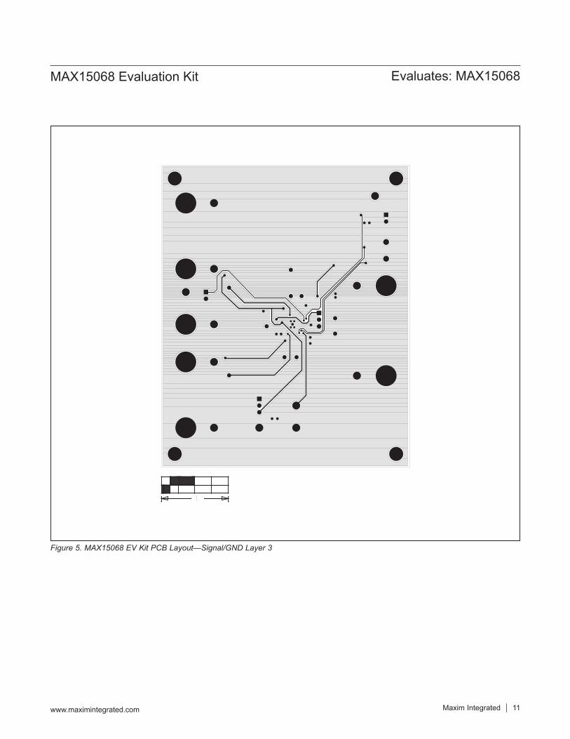
Figure 5. MAX15068 EV Kit PCB Layout—Signal/GND Layer 3
Maxim Integrated 12www.maximintegrated.com
Evaluates: MAX15068MAX15068 Evaluation Kit
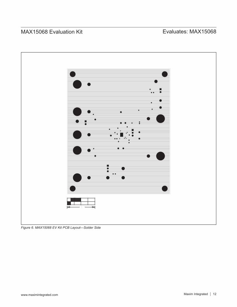
Figure 6. MAX15068 EV Kit PCB Layout—Solder Side
Maxim Integrated 13www.maximintegrated.com
Evaluates: MAX15068MAX15068 Evaluation Kit
#Denotes RoHS compliant.
PART TYPEMAX15068EVKIT# EV Kit
Ordering Information

Maxim Integrated cannot assume responsibility for use of any circuitry other than circuitry entirely embodied in a Maxim Integrated product. No circuit patent licenses are implied. Maxim Integrated reserves the right to change the circuitry and specifications without notice at any time.
Maxim Integrated and the Maxim Integrated logo are trademarks of Maxim Integrated Products, Inc. © 2019 Maxim Integrated Products, Inc. 14
Evaluates: MAX15068MAX15068 Evaluation Kit
REVISIONNUMBER
REVISIONDATE DESCRIPTION PAGES
CHANGED
0 1/14 Initial release —1 10/19 Corrected Procedure, equations, and description. All
Revision History
For pricing, delivery, and ordering information, please visit Maxim Integrated’s online storefront at https://www.maximintegrated.com/en/storefront/storefront.html.