Embed Size (px)
Citation preview
General DescriptionThe MAX3735A is a +3.3V laser driver for SFP/SFF appli-cations from 155Mbps up to 2.7Gbps. The device accepts differential input data and provides bias and modulation currents for driving a laser. DC-coupling to the laser allows for multirate applications and reduces the number of exter-nal components. The MAX3735A is fully compliant with the SFP MSA timing and the SFF-8472 transmit diagnostic requirements.An automatic power-control (APC) feedback loop is incor-porated to maintain a constant average optical power over temperature and lifetime. The wide modulation current range of 10mA to 60mA (up to 85mA AC-coupled) and bias current of 1mA to 100mA make this product ideal for driving FP/DFB laser diodes in fiber-optic modules. The resistor range for the laser current settings is optimized to interface with the DS1858 SFP controller IC.The MAX3735A provides transmit-disable control, a single-point latched transmit-failure monitor output, photo-current monitoring, and bias-current monitoring to indicate when the APC loop is unable to maintain the average optical power.The MAX3735A is available in a 4mm x 4mm TQFN pack-age and operates over the extended temperature range of -40°C to +85°C.
Applications Gigabit Ethernet SFP/SFF Transceiver Modules 1G/2G Fibre Channel SFP/SFF Transceiver Modules Multirate OC3 to OC48-FEC SFP/SFF Transceiver
Modules
Features Fully Compliant with SFP and SFF-8472 MSAs Programmable Modulation Current from 10mA to
60mA (DC-Coupled) Programmable Modulation Current from 10mA to
85mA (AC-Coupled) Programmable Bias Current from 1mA to 100mA Edge Transition Times <51ps 27mA (typ) Power-Supply Current Multirate 155Mbps to 2.7Gbps Operation Automatic Average Power Control On-Chip Pullup Resistor for TX_DISABLE 24-Pin 4mm x 4mm TQFN package
19-2529; Rev 4; 1/13
Ordering Information appears at end of data sheet.
IN+0.1µF
GND
MODS
ET
APCS
ET
APCF
ILT2
APCF
ILT1
SHUT
DOW
N
TX_F
AULT
TX_D
ISAB
LE
BC_M
ON
PC_M
ON MD
BIAS
OUT+OUT+
OUT-
OPTIONAL SHUTDOWNCIRCUITRY
V CC
IN-
REPRESENTS A CONTROLLED-IMPEDANCE TRANSMISSION LINE
SERDES MAX3735A0.1µF
+3.3V
+3.3V
CMD
FERRITE BEAD
+3.3V
10Ω
RBC_MON
RPC_MON
15Ω 0.01µF
DS1858/DS1859CONTROLLER
IC CAPC
M0N2
M0N3
MON1H1
H0
+3.3V
MAX3735A 2.7Gbps, Low-Power SFP Laser Driver
Typical Application Circuit
EVALUATION KIT AVAILABLE
Supply Voltage, VCC ............................................-0.5V to +6.0VCurrent into BIAS, OUT+, OUT- ..................... -20mA to +150mACurrent into MD .................................................... -5mA to +5mAVoltage at IN+, IN-, TX_DISABLE, TX_FAULT,
SHUTDOWN......................................... -0.5V to (VCC + 0.5V)Voltage at BIAS, PC_MON, BC_MON,
MODSET, APCSET .............................. -0.5V to (VCC + 0.5V)Voltage at OUT+, OUT- ........................... +0.5V to (VCC + 1.5V)Voltage at APCFILT1, APCFILT2 .............................-0.5V to +3V
Continuous Power Dissipation (TA = +70°C ) 24-Lead Thin QFN (derate 27.8mW/°C above +70°C) ............................................................2222mW
Operating Ambient Temperature Range (TA) ..... -40°C to +85°CStorage Ambient Temperature Range .............. -55°C to +150°CDie Attach Temperature ...................................................+400°CLead Temperature (soldering, 10s) .................................+300°C
PACKAGE TYPE: 24-PIN TQFNPackage Code T2444+3Outline Number 21-0139Land Pattern Number 90-0021
www.maximintegrated.com Maxim Integrated 2
MAX3735A 2.7Gbps, Low-Power SFP Laser Driver
Absolute Maximum Ratings
Stresses beyond those listed under “Absolute Maximum Ratings” may cause permanent damage to the device. These are stress ratings only, and functional operation of the device at these or any other conditions beyond those indicated in the operational sections of the specifications is not implied. Exposure to absolute maximum rating conditions for extended periods may affect device reliability.
Package Information
For the latest package outline information and land patterns (footprints), go to www.maximintegrated.com/packages. Note that a “+”, “#”, or “-” in the package code indicates RoHS status only. Package drawings may show a different suffix character, but the drawing pertains to the package regardless of RoHS status.
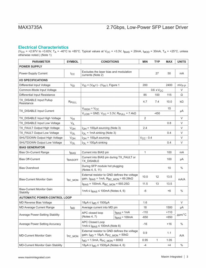
(VCC = +2.97V to +3.63V, TA = -40°C to +85°C. Typical values at VCC = +3.3V, IBIAS = 20mA, IMOD = 30mA, TA = +25°C, unless otherwise noted.) (Note 1)
PARAMETER SYMBOL CONDITIONS MIN TYP MAX UNITSPOWER SUPPLY
Power-Supply Current ICCExcludes the laser bias and modulation currents (Note 2) 27 50 mA
I/O SPECIFICATIONSDifferential Input Voltage VID VID = (VIN+) - (VIN-), Figure 1 200 2400 mVP-PCommon-Mode Input Voltage 0.6 x VCC VDifferential Input Resistance 85 100 115 Ω
TX_DISABLE Input Pullup Resistance RPULL 4.7 7.4 10.0 kΩ
TX_DISABLE Input CurrentVHIGH = VCC 15
µAVLOW = GND, VCC = 3.3V, RPULL = 7.4kΩ -450
TX_DISABLE Input High Voltage VIH 2 VTX_DISABLE Input Low Voltage VIL 0.8 VTX_FAULT Output High Voltage VOH IOH = 100µA sourcing (Note 3) 2.4 VTX_FAULT Output Low Voltage VOL IOL = 1mA sinking (Note 3) 0.4 VSHUTDOWN Output High Voltage VOH IOH = 100µA sourcing VCC - 0.4 VSHUTDOWN Output Low Voltage VOL IOL = 100µA sinking 0.4 VBIAS GENERATORBias On-Current Range IBIAS Current into BIAS pin 1 100 mA
Bias Off-Current IBIASOFFCurrent into BIAS pin during TX_FAULT or TX_DISABLE 100 µA
Bias Overshoot During SFP module hot plugging (Notes 4, 5, 11) 10 %
Bias-Current Monitor Gain IBC_MON
External resistor to GND defines the voltage gain, IBIAS = 1mA, RBC_MON = 69.28kΩ 10.0 12 13.5
mA/AIBIAS = 100mA, RBC_MON = 693.25Ω 11.5 13 13.5
Bias-Current Monitor Gain Stability 1mA ≤ IBIAS ≤ 100mA (Notes 4, 6) -6 +6 %
AUTOMATIC POWER-CONTROL LOOPMD Reverse Bias Voltage 18µA ≤ IMD ≤ 1500µA 1.6 VMD Average Current Range IMD Average current into MD pin 18 1500 µA
Average Power-Setting Stability APC closed loop (Notes 4, 7)
IBIAS = 1mA -110 +110ppm/°C
IBIAS = 100mA -650 +650
Average Power Setting Accuracy APC Closed Loop 1mA ≤ IBIAS ≤ 100mA (Note 8) -16 +16 %
MD-Current Monitor Gain IPC_MON
External resistor to GND defines the voltage gain; IMD = 18µA, RPC_MON = 50kΩ 0.9 1.1
A/AIMD = 1.5mA, RPC_MON = 600Ω 0.95 1 1.05
MD-Current Monitor Gain Stability 18µA ≤ IMD ≤ 1500µA (Notes 4, 6) -4 +4 %
www.maximintegrated.com Maxim Integrated 3
MAX3735A 2.7Gbps, Low-Power SFP Laser Driver
Electrical Characteristics
(VCC = +2.97V to +3.63V, TA = -40°C to +85°C. Typical values at VCC = +3.3V, IBIAS = 20mA, IMOD = 30mA, TA = +25°C, unless otherwise noted.) (Note 1)
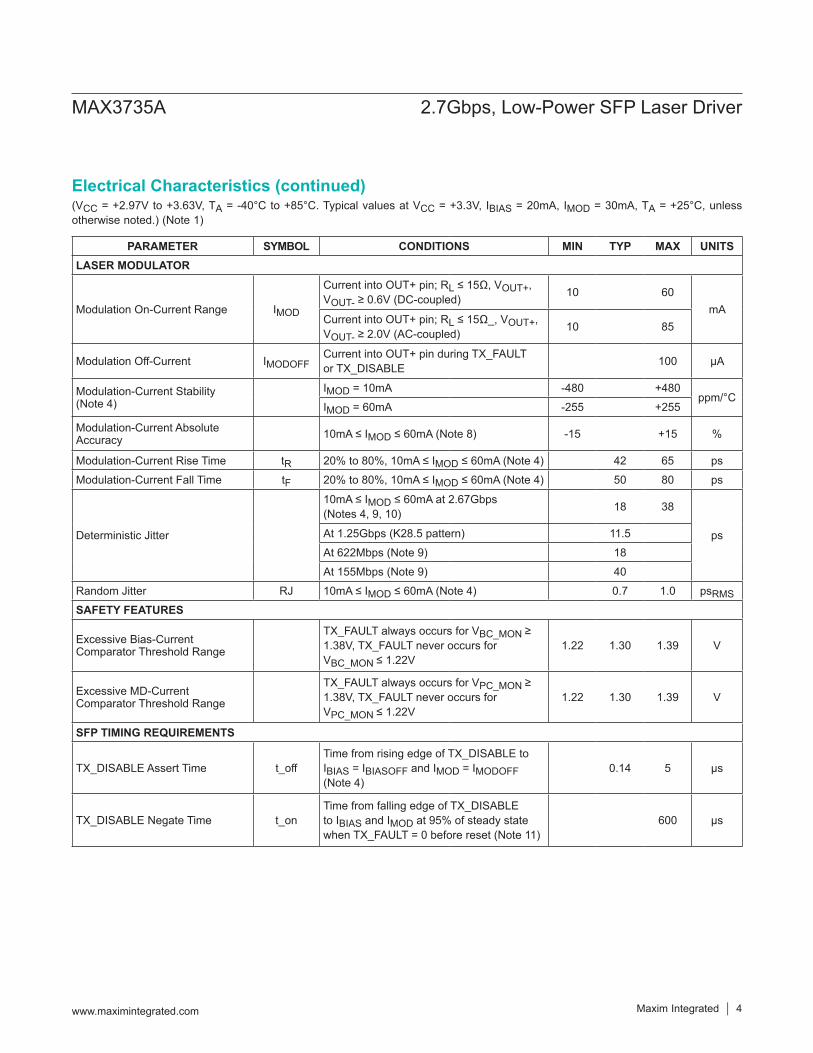
PARAMETER SYMBOL CONDITIONS MIN TYP MAX UNITSLASER MODULATOR
Modulation On-Current Range IMOD
Current into OUT+ pin; RL ≤ 15Ω, VOUT+, VOUT- ≥ 0.6V (DC-coupled) 10 60
mACurrent into OUT+ pin; RL ≤ 15Ω_, VOUT+, VOUT- ≥ 2.0V (AC-coupled) 10 85
Modulation Off-Current IMODOFFCurrent into OUT+ pin during TX_FAULT or TX_DISABLE 100 µA
Modulation-Current Stability (Note 4)
IMOD = 10mA -480 +480ppm/°C
IMOD = 60mA -255 +255
Modulation-Current Absolute Accuracy 10mA ≤ IMOD ≤ 60mA (Note 8) -15 +15 %
Modulation-Current Rise Time tR 20% to 80%, 10mA ≤ IMOD ≤ 60mA (Note 4) 42 65 psModulation-Current Fall Time tF 20% to 80%, 10mA ≤ IMOD ≤ 60mA (Note 4) 50 80 ps
Deterministic Jitter
10mA ≤ IMOD ≤ 60mA at 2.67Gbps (Notes 4, 9, 10) 18 38
psAt 1.25Gbps (K28.5 pattern) 11.5At 622Mbps (Note 9) 18At 155Mbps (Note 9) 40
Random Jitter RJ 10mA ≤ IMOD ≤ 60mA (Note 4) 0.7 1.0 psRMSSAFETY FEATURES
Excessive Bias-Current Comparator Threshold Range
TX_FAULT always occurs for VBC_MON ≥ 1.38V, TX_FAULT never occurs for VBC_MON ≤ 1.22V
1.22 1.30 1.39 V
Excessive MD-Current Comparator Threshold Range
TX_FAULT always occurs for VPC_MON ≥ 1.38V, TX_FAULT never occurs for VPC_MON ≤ 1.22V
1.22 1.30 1.39 V
SFP TIMING REQUIREMENTS
TX_DISABLE Assert Time t_offTime from rising edge of TX_DISABLE to IBIAS = IBIASOFF and IMOD = IMODOFF (Note 4)
0.14 5 µs
TX_DISABLE Negate Time t_onTime from falling edge of TX_DISABLE to IBIAS and IMOD at 95% of steady state when TX_FAULT = 0 before reset (Note 11)
600 µs
www.maximintegrated.com Maxim Integrated 4
MAX3735A 2.7Gbps, Low-Power SFP Laser Driver
Electrical Characteristics (continued)
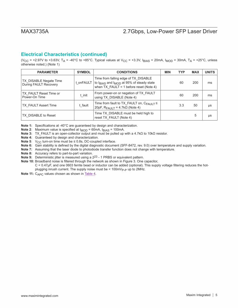
(VCC = +2.97V to +3.63V, TA = -40°C to +85°C. Typical values at VCC = +3.3V, IBIAS = 20mA, IMOD = 30mA, TA = +25°C, unless otherwise noted.) (Note 1)
Note 1: Specifications at -40°C are guaranteed by design and characterization.Note 2: Maximum value is specified at IMOD = 60mA, IBIAS = 100mA.Note 3: TX_FAULT is an open-collector output and must be pulled up with a 4.7kΩ to 10kΩ resistor.Note 4: Guaranteed by design and characterization.Note 5: VCC turn-on time must be ≤ 0.8s, DC-coupled interface.Note 6: Gain stability is defined by the digital diagnostic document (SFF-8472, rev. 9.0) over temperature and supply variation.Note 7: Assuming that the laser diode to photodiode transfer function does not change with temperature.Note 8: Accuracy refers to part-to-part variation.Note 9: Deterministic jitter is measured using a 223 - 1 PRBS or equivalent pattern.Note 10: Broadband noise is filtered through the network as shown in Figure 3. One capacitor,
C < 0.47μF, and one 0603 ferrite bead or inductor can be added (optional). This supply voltage filtering reduces the hot- plugging inrush current. The supply noise must be < 100mVP-P up to 2MHz.
Note 11: CAPC values chosen as shown in Table 4.
PARAMETER SYMBOL CONDITIONS MIN TYP MAX UNITS
TX_DISABLE Negate Time During FAULT Recovery t_onFAULT
Time from falling edge of TX_DISABLE to IBIAS and IMOD at 95% of steady state when TX_FAULT = 1 before reset (Note 4)
60 200 ms
TX_FAULT Reset Time or Power-On Time t_init From power-on or negation of TX_FAULT
using TX_DISABLE (Note 4) 60 200 ms
TX_FAULT Assert Time t_fault Time from fault to TX_FAULT on, CFAULT ≤ 20pF, RFAULT = 4.7kΩ (Note 4) 3.3 50 µs
TX_DISABLE to Reset Time TX_DISABLE must be held high to reset TX_FAULT (Note 4) 5 µs
www.maximintegrated.com Maxim Integrated 5
MAX3735A 2.7Gbps, Low-Power SFP Laser Driver
Electrical Characteristics (continued)
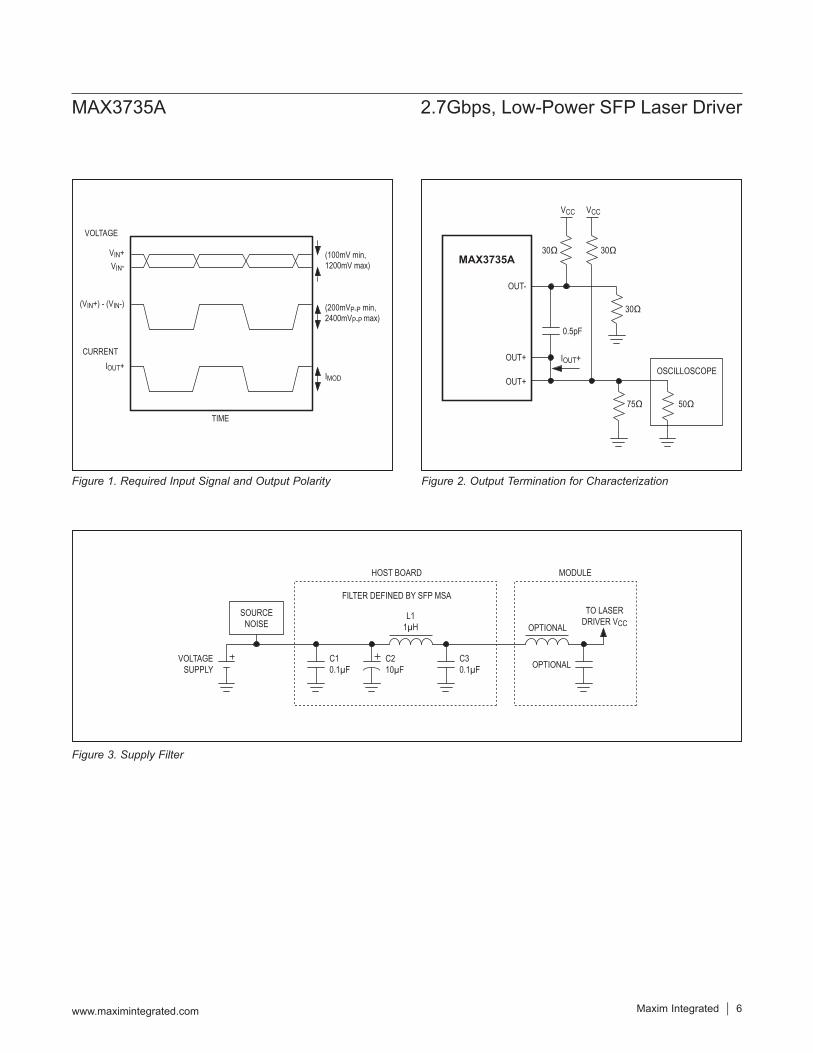
Figure 1. Required Input Signal and Output Polarity Figure 2. Output Termination for Characterization
Figure 3. Supply Filter
VIN+
(VIN+) - (VIN-)
VIN-
(200mVP-P min,2400mVP-P max)
(100mV min,1200mV max)
IMOD
VOLTAGE
CURRENT
TIME
IOUT+
50Ω75Ω
30Ω
30Ω
0.5pF
30Ω
OSCILLOSCOPEOUT+
IOUT+
OUT-
OUT+
MAX3735A
VCC VCC
SOURCENOISE
TO LASERDRIVER VCCOPTIONAL
OPTIONAL
MODULEHOST BOARD
C10.1µF
C210µF
C30.1µF
L11µH
VOLTAGESUPPLY
FILTER DEFINED BY SFP MSA
www.maximintegrated.com Maxim Integrated 6
MAX3735A 2.7Gbps, Low-Power SFP Laser Driver
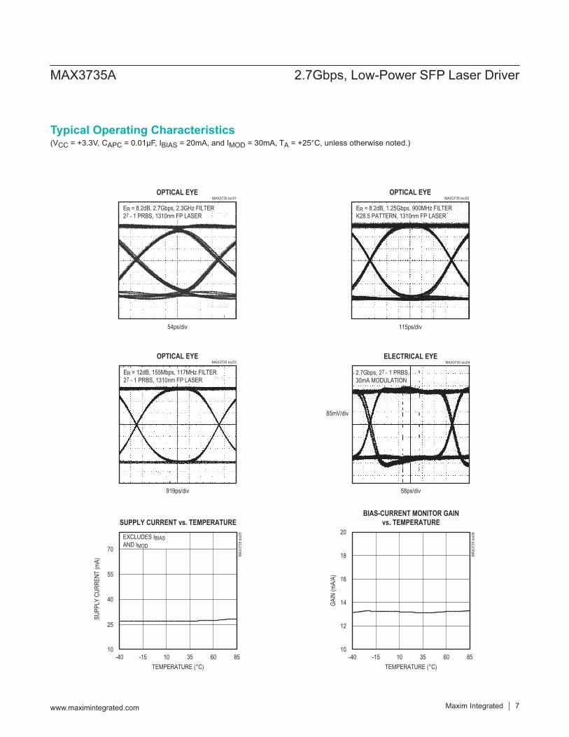
(VCC = +3.3V, CAPC = 0.01μF, IBIAS = 20mA, and IMOD = 30mA, TA = +25°C, unless otherwise noted.)
OPTICAL EYEMAX3735 toc02
115ps/div
ER = 8.2dB, 1.25Gbps, 900MHz FILTERK28.5 PATTERN, 1310nm FP LASER
ELECTRICAL EYEMAX3735 toc04
58ps/div
2.7Gbps, 27 - 1 PRBS, 30mA MODULATION
85mV/div
BIAS-CURRENT MONITOR GAINvs. TEMPERATURE
MAX
3735
toc0
6
TEMPERATURE (°C)
GAIN
(mA/
A)
603510-15
12
14
16
18
20
10-40 85
OPTICAL EYEMAX3735 toc01
54ps/div
ER = 8.2dB, 2.7Gbps, 2.3GHz FILTER27 - 1 PRBS, 1310nm FP LASER
OPTICAL EYEMAX3735 toc03
919ps/div
ER = 12dB, 155Mbps, 117MHz FILTER27 - 1 PRBS, 1310nm FP LASER
SUPPLY CURRENT vs. TEMPERATURE
MAX
3735
toc0
5
TEMPERATURE (°C)
SUPP
LY C
URRE
NT (m
A)
603510-15
25
40
55
70
10-40 85
EXCLUDES IBIASAND IMOD
Maxim Integrated 7www.maximintegrated.com
MAX3735A 2.7Gbps, Low-Power SFP Laser Driver
Typical Operating Characteristics
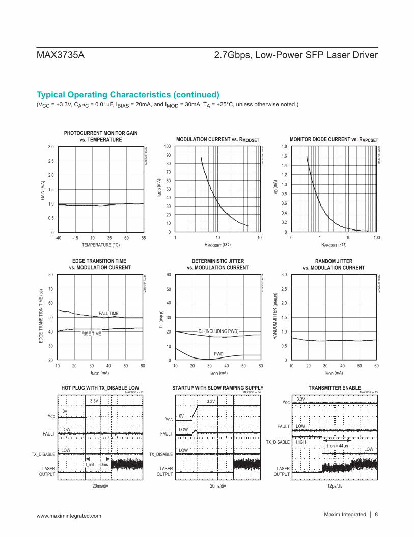
(VCC = +3.3V, CAPC = 0.01μF, IBIAS = 20mA, and IMOD = 30mA, TA = +25°C, unless otherwise noted.)
MONITOR DIODE CURRENT vs. RAPCSET
MAX
3735
toc0
9
RAPCSET (kΩ)
I MD
(mA)
101
0.2
0.4
0.6
0.8
1.0
1.2
1.4
1.6
1.8
00 100
MODULATION CURRENT vs. RMODSET
MAX
3735
toc0
8
RMODSET (kΩ)
I MOD
(mA)
10
10
20
30
40
50
60
70
80
90
100
01 100
RANDOM JITTERvs. MODULATION CURRENT
MAX
3735
toc1
2
IMOD (mA)
RAND
OM JI
TTER
(ps R
MS)
50403020
0.5
1.0
1.5
2.0
2.5
3.0
010 60
DETERMINISTIC JITTERvs. MODULATION CURRENT
IMOD (mA)
DJ (p
s P-P
)
50403020
10
20
30
50
40
60
010 60
DJ (INCLUDING PWD)
PWD
MAX
3735
toc1
1
TRANSMITTER ENABLEMAX3735 toc15
12µs/div
FAULT
VCC
LASEROUTPUT
TX_DISABLEt_on = 44µs
LOW
HIGH
3.3V
LOW
STARTUP WITH SLOW RAMPING SUPPLYMAX3735 toc14
20ms/div
FAULT
VCC
LASEROUTPUT
TX_DISABLE
LOW
0V
LOW
3.3V
PHOTOCURRENT MONITOR GAINvs. TEMPERATURE
MAX
3735
toc0
7
TEMPERATURE (°C)
GAIN
(A/A
)
603510-15
0.5
1.0
1.5
2.0
2.5
3.0
0-40 85
EDGE TRANSITION TIME vs. MODULATION CURRENT
MAX
3735
toc1
0
IMOD (mA)
EDGE
TRA
NSIT
ION
TIME
(ps)
50403020
30
40
50
60
70
80
2010 60
RISE TIME
FALL TIME
HOT PLUG WITH TX_DISABLE LOWMAX3735 toc13
20ms/div
FAULT
VCC
LASEROUTPUT
TX_DISABLE
t_init = 60ms
LOW
LOW
0V
3.3V
Maxim Integrated 8www.maximintegrated.com
MAX3735A 2.7Gbps, Low-Power SFP Laser Driver
Typical Operating Characteristics (continued)
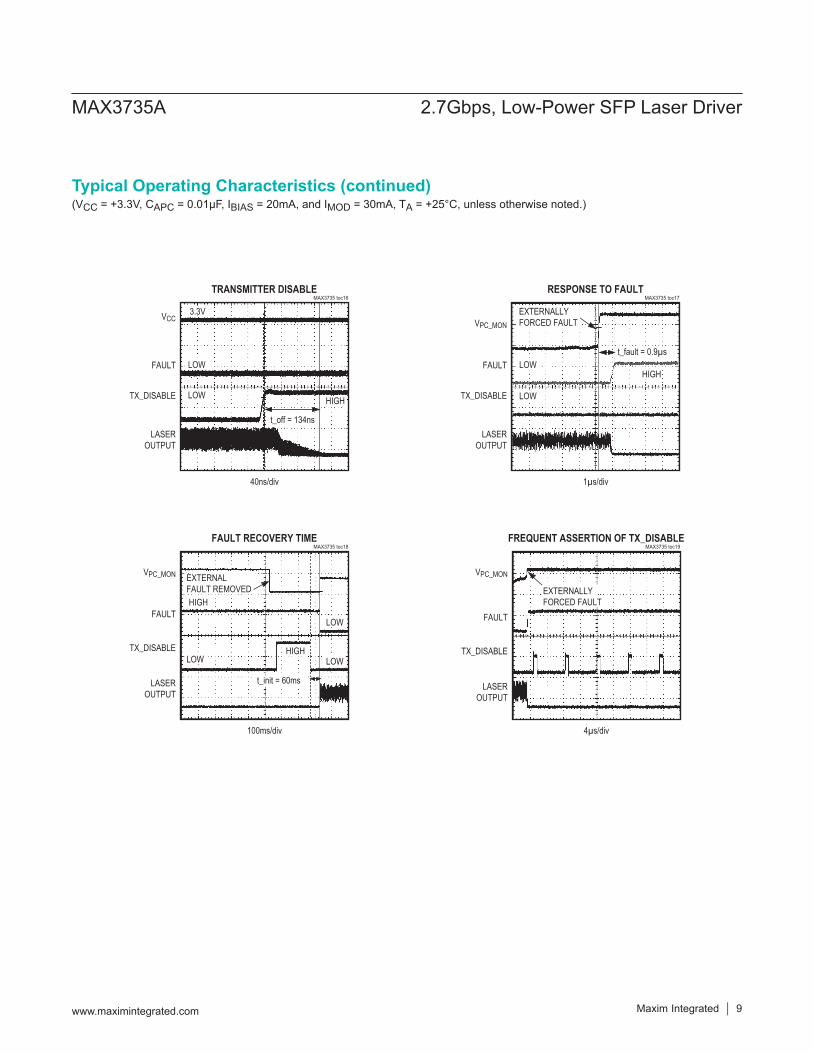
(VCC = +3.3V, CAPC = 0.01μF, IBIAS = 20mA, and IMOD = 30mA, TA = +25°C, unless otherwise noted.)
RESPONSE TO FAULTMAX3735 toc17
1µs/div
FAULT
VPC_MON
LASEROUTPUT
TX_DISABLE
t_fault = 0.9µsLOW
LOW
EXTERNALLYFORCED FAULT
HIGH
FREQUENT ASSERTION OF TX_DISABLEMAX3735 toc19
4µs/div
FAULT
VPC_MON
LASEROUTPUT
TX_DISABLE
EXTERNALLYFORCED FAULT
TRANSMITTER DISABLEMAX3735 toc16
40ns/div
FAULT
VCC
LASEROUTPUT
TX_DISABLE
t_off = 134ns
LOW
LOW
3.3V
HIGH
FAULT RECOVERY TIMEMAX3735 toc18
100ms/div
FAULT
VPC_MON
LASEROUTPUT
TX_DISABLE
t_init = 60ms
HIGH
LOW
EXTERNAL FAULT REMOVED
HIGH
LOW
LOW
Maxim Integrated 9www.maximintegrated.com
MAX3735A 2.7Gbps, Low-Power SFP Laser Driver
Typical Operating Characteristics (continued)
22
MAX3735A
2324 21 20 19
7 8 9 10 11 12
1
2
3
4
5
6
18
17
16
15
14
13
VCC
Thin QFN*(4mm x 4mm)
TOP VIEW
IN+
IN-
VCC
PC_MON
BC_MON
VCC
OUT-
OUT+
OUT+
VCC
BIAS
GND
V CC
SHUT
DOW
N
TX_F
AULT
MODS
ET
GND
TX_D
ISAB
LE
APCS
ET
GND
APCF
ILT2
APCF
ILT1
MD
*THE EXPOSED PAD MUST BE CONNECTED TO CIRCUIT BOARD GROUNDFOR PROPER THERMAL AND ELECTRICAL PERFORMANCE.
www.maximintegrated.com Maxim Integrated 10
MAX3735A 2.7Gbps, Low-Power SFP Laser Driver
Pin Configuration

Detailed DescriptionThe MAX3735A laser driver consists of three parts: a high-speed modulation driver, a laser-biasing block with automatic power control (APC), and safety circuitry (Functional Diagram). The circuit design is optimized for high-speed and low-voltage (+3.3V) operation.
High-Speed Modulation DriverThe output stage is composed of a high-speed differen-tial pair and a programmable modulation current source. The MAX3735A is optimized for driving a 15Ω load; the minimum instantaneous voltage required at OUT+ is 0.6V. Modulation current swings up to 60mA are possible when the laser diode is DC-coupled to the driver and up to 85mA when the laser diode is AC-coupled to the driver.
To interface with the laser diode, a damping resistor (RD) is required for impedance matching. The combined resis-tance of the series damping resistor and the equivalent series resistance of the laser diode should equal 15Ω. To reduce optical output aberrations and duty-cycle distortion caused by laser diode parasitic inductance, an RC shunt network might be necessary. Refer to Maxim Application Note HFAN 02.0: Interfacing Maxim’s Laser Drivers to Laser Diodes for more information.At data rates of 2.7Gbps, any capacitive load at the cath-ode of a laser diode degrades optical output performance. Because the BIAS output is directly connected to the laser cathode, minimize the parasitic capacitance associated with the pin by using an inductor to isolate the BIAS pin parasitics from the laser cathode.
PIN NAME FUNCTION1, 4, 8, 14, 18 VCC +3.3V Supply Voltage
2 IN+ Noninverted Data Input3 IN- Inverted Data Input
5 PC_MON Photodiode Current Monitor Output. Current out of this pin develops a ground-referenced voltage across an external resistor that is proportional to the monitor diode current.
6 BC_MON Bias Current Monitor Output. Current out of this pin develops a ground-referenced voltage across an external resistor that is proportional to the bias current.
7, 12, 22 GND Ground
9 SHUTDOWN Shutdown Driver Output. Voltage output to control an external transistor for optional shutdown circuitry.
10 TX_FAULT Open-Collector Transmit Fault Indicator (Table 1).11 MODSET A resistor connected from this pad to ground sets the desired modulation current.13 BIAS Laser Bias Current Output
15, 16 OUT+ Noninverted Modulation Current Output. Connect pins 15 and 16 externally to minimize parasitic inductance of the package. IMOD flows into this pin when input data is high.
17 OUT- Inverted Modulation Current Output. IMOD flows into this pin when input data is low.
19 MD Monitor Diode Input. Connect this pin to the anode of a monitor photodiode. A capacitor to ground is required to filter the high-speed AC monitor photocurrent.
20 APCFILT1 Connect a capacitor (CAPC) between pin 20 (APCFILT1) and pin 21 (APCFILT2) to set the dominant pole of the APC feedback loop.
21 APCFILT2 See APCFILT123 APCSET A resistor connected from this pin to ground sets the desired average optical power.
24 TX_DISABLE Transmitter Disable, TTL. Laser output is disabled when TX_DISABLE is asserted high or left unconnected. The laser output is enabled when this pin is asserted low.
EP Exposed Pad Ground. Must be soldered to the circuit board ground for proper thermal and electrical performance (see the Exposed-Pad Package section).
www.maximintegrated.com Maxim Integrated 11
MAX3735A 2.7Gbps, Low-Power SFP Laser Driver
Pin Description
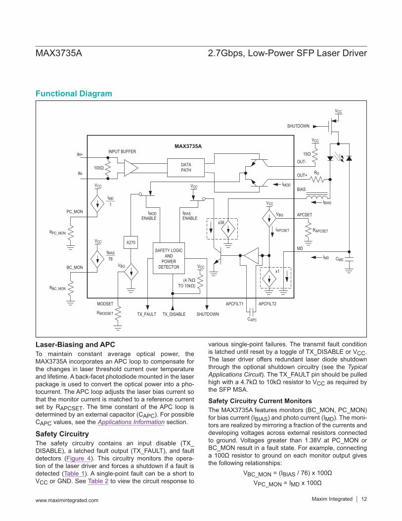
Laser-Biasing and APCTo maintain constant average optical power, the MAX3735A incorporates an APC loop to compensate for the changes in laser threshold current over temperature and lifetime. A back-facet photodiode mounted in the laser package is used to convert the optical power into a pho-tocurrent. The APC loop adjusts the laser bias current so that the monitor current is matched to a reference current set by RAPCSET. The time constant of the APC loop is determined by an external capacitor (CAPC). For possible CAPC values, see the Applications Information section.
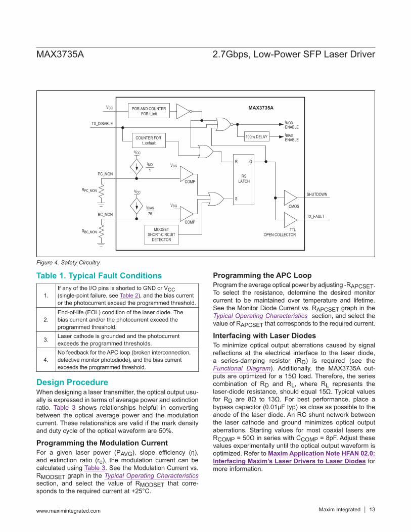
Safety CircuitryThe safety circuitry contains an input disable (TX_DISABLE), a latched fault output (TX_FAULT), and fault detectors (Figure 4). This circuitry monitors the opera-tion of the laser driver and forces a shutdown if a fault is detected (Table 1). A single-point fault can be a short to VCC or GND. See Table 2 to view the circuit response to
various single-point failures. The transmit fault condition is latched until reset by a toggle of TX_DISABLE or VCC. The laser driver offers redundant laser diode shutdown through the optional shutdown circuitry (see the Typical Applications Circuit). The TX_FAULT pin should be pulled high with a 4.7kΩ to 10kΩ resistor to VCC as required by the SFP MSA.
Safety Circuitry Current MonitorsThe MAX3735A features monitors (BC_MON, PC_MON) for bias current (IBIAS) and photo current (IMD). The moni-tors are realized by mirroring a fraction of the currents and developing voltages across external resistors connected to ground. Voltages greater than 1.38V at PC_MON or BC_MON result in a fault state. For example, connecting a 100Ω resistor to ground on each monitor output gives the following relationships:
VBC_MON = (IBIAS / 76) x 100ΩVPC_MON = IMD x 100Ω
Functional Diagram
VCC
VCC
IAPCSET
CAPC
IBIAS
IMOD
RD
IMD
RAPCSET
x38
VCC
RPC_MON
PC_MON
100ΩIN-
IN+
IMODENABLE
IBIASENABLE
INPUT BUFFER
SHUTDOWN
DATAPATH
X270SAFETY LOGIC
ANDPOWER
DETECTOR
TX_FAULT
CMD
TX_DISABLE
APCFILT1 APCFILT2
SHUTDOWN
MODSET
BC_MONx1
76IBIAS
1IMD
APCSET
MD
MAX3735A
VCC
VBG
(4.7kΩTO 10kΩ)RBC_MON
VCC
VBG
RMODSET
VCC
OUT-
OUT+
BIAS
VCC
15Ω
www.maximintegrated.com Maxim Integrated 12
MAX3735A 2.7Gbps, Low-Power SFP Laser Driver
Design ProcedureWhen designing a laser transmitter, the optical output usu-ally is expressed in terms of average power and extinction ratio. Table 3 shows relationships helpful in converting between the optical average power and the modulation current. These relationships are valid if the mark density and duty cycle of the optical waveform are 50%.
Programming the Modulation CurrentFor a given laser power (PAVG), slope efficiency (η), and extinction ratio (re), the modulation current can be calculated using Table 3. See the Modulation Current vs. RMODSET graph in the Typical Operating Characteristics section, and select the value of RMODSET that corre-sponds to the required current at +25°C.
Programming the APC LoopProgram the average optical power by adjusting -RAPCSET. To select the resistance, determine the desired monitor current to be maintained over temperature and lifetime. See the Monitor Diode Current vs. RAPCSET graph in the Typical Operating Characteristics section, and select the value of RAPCSET that corresponds to the required current.
Interfacing with Laser DiodesTo minimize optical output aberrations caused by signal reflections at the electrical interface to the laser diode, a series-damping resistor (RD) is required (see the Functional Diagram). Additionally, the MAX3735A out-puts are optimized for a 15Ω load. Therefore, the series combination of RD and RL, where RL represents the laser-diode resistance, should equal 15Ω. Typical values for RD are 8Ω to 13Ω. For best performance, place a bypass capacitor (0.01μF typ) as close as possible to the anode of the laser diode. An RC shunt network between the laser cathode and ground minimizes optical output aberrations. Starting values for most coaxial lasers are RCOMP = 50Ω in series with CCOMP = 8pF. Adjust these values experimentally until the optical output waveform is optimized. Refer to Maxim Application Note HFAN 02.0: Interfacing Maxim’s Laser Drivers to Laser Diodes for more information.
Figure 4. Safety Circuitry
Table 1. Typical Fault Conditions
1.If any of the I/O pins is shorted to GND or VCC (single-point failure, see Table 2), and the bias current or the photocurrent exceed the programmed threshold.
2.End-of-life (EOL) condition of the laser diode. The bias current and/or the photocurrent exceed the programmed threshold.
3. Laser cathode is grounded and the photocurrent exceeds the programmed thresholds.
4.No feedback for the APC loop (broken interconnection, defective monitor photodiode), and the bias current exceeds the programmed threshold.
POR AND COUNTERFOR t_init
COUNTER FOR t_onfault
MODSETSHORT-CIRCUIT
DETECTOR
100ns DELAY
MAX3735A
VCC
VCC
VCC
VBG
COMP
VBG
COMP
76IBIAS
1IMD
RSLATCH
R Q
S
PC_MON
BC_MON
IMODENABLE
IBIASENABLE
TX_FAULT
CMOS
TTLOPEN COLLECTOR
SHUTDOWNRPC_MON
RBC_MON
TX_DISABLE
www.maximintegrated.com Maxim Integrated 13
MAX3735A 2.7Gbps, Low-Power SFP Laser Driver
Pattern-Dependent JitterTo minimize the pattern-dependent jitter associated with the APC loop time constant, and to guarantee loop stability, connect a capacitor between APCFILT1 and APCFILT2 (see the Applications Information section for more information about choosing CAPC values). A capaci-tor attached to the photodiode anode (CMD) is also rec-ommended to filter transient currents that originate from the photodiode. To maintain stability and proper phase margin associated with the two poles created by CAPC and CMD. CAPC should be 4x to 20x greater than CMD.
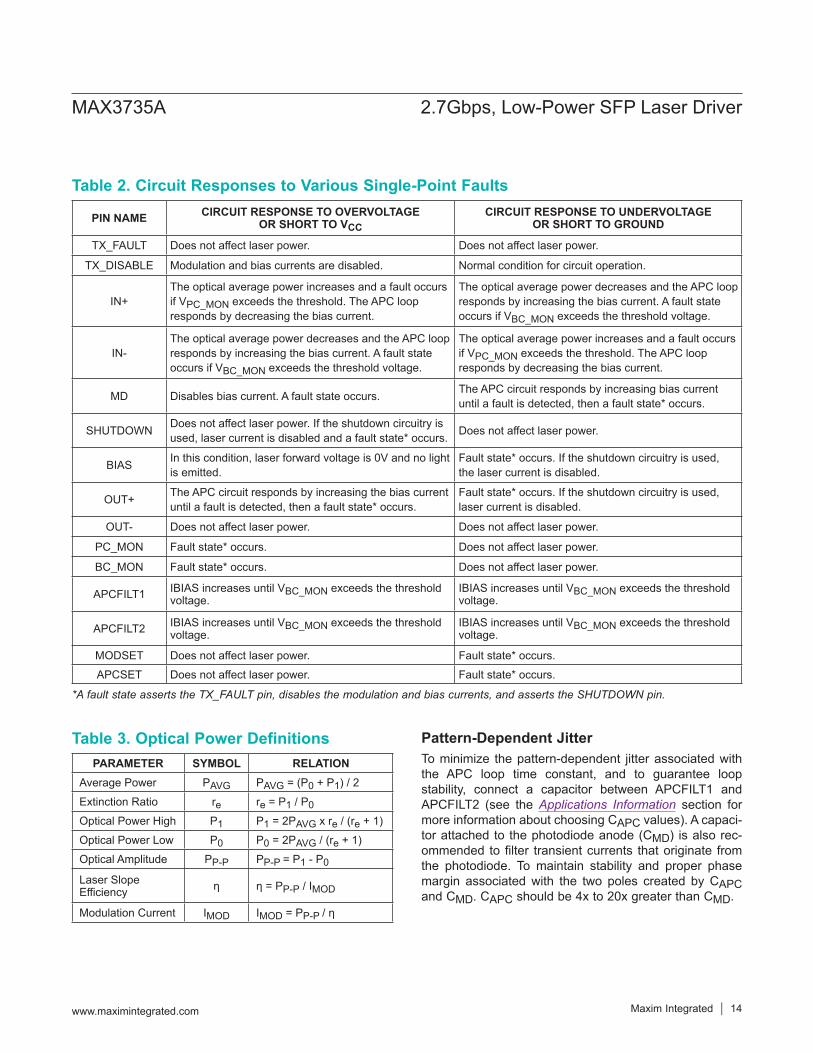
Table 2. Circuit Responses to Various Single-Point Faults
Table 3. Optical Power Definitions
*A fault state asserts the TX_FAULT pin, disables the modulation and bias currents, and asserts the SHUTDOWN pin.
PIN NAME CIRCUIT RESPONSE TO OVERVOLTAGE OR SHORT TO VCC
CIRCUIT RESPONSE TO UNDERVOLTAGE OR SHORT TO GROUND
TX_FAULT Does not affect laser power. Does not affect laser power.
TX_DISABLE Modulation and bias currents are disabled. Normal condition for circuit operation.
IN+The optical average power increases and a fault occurs if VPC_MON exceeds the threshold. The APC loop responds by decreasing the bias current.
The optical average power decreases and the APC loop responds by increasing the bias current. A fault state occurs if VBC_MON exceeds the threshold voltage.
IN-The optical average power decreases and the APC loop responds by increasing the bias current. A fault state occurs if VBC_MON exceeds the threshold voltage.
The optical average power increases and a fault occurs if VPC_MON exceeds the threshold. The APC loop responds by decreasing the bias current.
MD Disables bias current. A fault state occurs. The APC circuit responds by increasing bias current until a fault is detected, then a fault state* occurs.
SHUTDOWN Does not affect laser power. If the shutdown circuitry is used, laser current is disabled and a fault state* occurs. Does not affect laser power.
BIAS In this condition, laser forward voltage is 0V and no light is emitted.
Fault state* occurs. If the shutdown circuitry is used, the laser current is disabled.
OUT+ The APC circuit responds by increasing the bias current until a fault is detected, then a fault state* occurs.
Fault state* occurs. If the shutdown circuitry is used, laser current is disabled.
OUT- Does not affect laser power. Does not affect laser power.
PC_MON Fault state* occurs. Does not affect laser power.
BC_MON Fault state* occurs. Does not affect laser power.
APCFILT1 IBIAS increases until VBC_MON exceeds the threshold voltage.
IBIAS increases until VBC_MON exceeds the threshold voltage.
APCFILT2 IBIAS increases until VBC_MON exceeds the threshold voltage.
IBIAS increases until VBC_MON exceeds the threshold voltage.
MODSET Does not affect laser power. Fault state* occurs.APCSET Does not affect laser power. Fault state* occurs.
PARAMETER SYMBOL RELATIONAverage Power PAVG PAVG = (P0 + P1) / 2Extinction Ratio re re = P1 / P0Optical Power High P1 P1 = 2PAVG x re / (re + 1)Optical Power Low P0 P0 = 2PAVG / (re + 1)Optical Amplitude PP-P PP-P = P1 - P0
Laser Slope Efficiency ƞ ƞ = PP-P / IMOD
Modulation Current IMOD IMOD = PP-P / ƞ
www.maximintegrated.com Maxim Integrated 14
MAX3735A 2.7Gbps, Low-Power SFP Laser Driver

Input Termination RequirementsThe MAX3735A data inputs are SFP MSA compliant. On-chip 100Ω differential input impedance is provided for optimal termination (Figure 5). Because of the on-chip biasing network, the inputs self-bias to the proper operat-ing point to accommodate AC-coupling.
Optional Shutdown Output CircuitryThe SHUTDOWN control output features extended eye safety when the laser cathode is grounded. An external transistor is required to implement this circuit (see the Functional Diagram). In the event of a fault, SHUTDOWN asserts high, placing the optional shutdown transistor in cutoff mode and thereby shutting off the laser current.
Applications InformationAn example of how to set up the MAX3735A follows:Select a communications-grade laser for 2.488Gbps. Assume that the laser output average power is PAVG = 0dBm, the operating temperature is -40°C to +85°C, mini-mum extinction ratio is 6.6 (8.2dB), and the laser diode has the following characteristics:
Wavelength: λ = 1.3μmThreshold current: ITH = 22mA at +25°CThreshold temperature coefficient: βTH = 1.3% / °CLaser-to-monitor transfer: ρMON = 0.2A/WLaser slope efficiency: η = 0.05mW/mA at +25°C
Determine RAPCSETThe desired monitor diode current is estimated by IMD = PAVG x ρMON = 200μA. The Monitor Diode vs. RAPCSET graph in the Typical Operating Characteristics section shows that RAPCSET should be 3kΩ. The value can also be estimated using the equation below:
IMD = 1.23 / (2 x RAPCSET)
Determine RMODSETTo achieve a minimum extinction ratio (re) of 6.6 over temperature and lifetime, calculate the required extinction ratio at +25°C. Assuming the results of the calculation are re = 20 at +25°C, the peak-to-peak optical power PP-P = 1.81mW, according to Table 3. The required modula-tion current is 1.81mW / (0.05mW/mA) = 36.2mA. The Modulation Current vs. RMODSET graph in the Typical Operating Characteristics section shows that RMODSET should be 9.5kΩ. The value can also be estimated using the equation below:
IMOD = 1.23 / (0.0037 x RMODSET)
Determine CAPCIn order to meet SFP timing requirements and minimize pattern-dependent jitter, the CAPC capacitor value is determined by the laser-to-monitor transfer and other variables. The following equations and Table 4 can be used to choose the CAPC values for the MAX3735A. The equations and Table 4 assume a DC-coupled laser. Refer to Maxim Application Note HFDN 23.0: Choosing the
Figure 5. Simplified Input Structure Figure 6. Simplified Output Structure
24kΩ
16kΩ
50Ω
50Ω
PACKAGE
0.97nH
0.97nH
0.11pF
0.11pF
VCC
VCC
MAX3735A
VCC
IN+
IN-
VCC
OUT-
OUT+
PACKAGE
0.99nH
MAX3735A
0.81nH
OUT+0.99nH
0.11pF
K = 0.3
0.11pF
0.11pF
www.maximintegrated.com Maxim Integrated 15
MAX3735A 2.7Gbps, Low-Power SFP Laser Driver
APC Loop Capacitors Used with MAX3735/MAX3735A SFP Module Designs for more information on choosing CAPC for DC- and AC-coupled laser interfaces.Use Table 4 to choose the CAPC capacitor value. CAPC should be chosen according to the highest gain of the lasers (generally at cold temperature). CAPC selection assumes a 34% reduction in the gain of the lasers at +85°C from the cold (-40°C) values.
where laser Gain = IMD/(IBIAS - ITH + 0.5 x IMOD) for DC-coupled lasers. CMD can then be chosen as approxi-mately 4x to 20x smaller than CAPC.
Using the MAX3735A with Digital PotentiometersFor more information on using the MAX3735A with the Dallas DS1858/DS1859 SFP controller, refer to Maxim Application Note HFAN 2.3.3: Optimizing the Resolution of Laser Driver Setting Using Linear Digital Potentiometers for more information.
Modulation Currents Exceeding 60mAFor applications requiring a modulation current greater than 60mA, headroom is insufficient for proper operation of the laser driver if the laser is DC-coupled. To avoid this problem, the MAX3735A’s modulation output can be AC-coupled to the cathode of a laser diode. An external pullup inductor is necessary to DC-bias the modulation output at VCC. Such a configuration isolates laser forward voltage from the output circuitry and allows the output at OUT+ to swing above and below the supply voltage (VCC).
When AC-coupled, the MAX3735A modulation current can be programmed from 10mA to 85mA. Refer to Maxim Application Note HFAN 02.0: Interfacing Maxim’s Laser Drivers to Laser Diodes for more information on ACcoupling laser drivers to laser diodes.
Interface ModelsFigure 5 and 6 show simplified input and output circuits for the MAX3735A laser driver.
Layout ConsiderationsTo minimize inductance, keep the connections between the MAX3735A output pins and laser diode as close as possible. Optimize the laser diode performance by plac-ing a bypass capacitor as close as possible to the laser anode. Use good high-frequency layout techniques and multiple-layer boards with uninterrupted ground planes to minimize EMI and crosstalk.
Exposed-Pad PackageThe exposed pad on the 24-pin QFN provides a very low thermal resistance path for heat removal from the IC. The pad is also electrical ground on the MAX3735A and must be soldered to the circuit board ground for proper thermal and electrical performance. Refer to Maxim Application Note HFAN-08.1: Thermal Considerations for QFN and Other Exposed-Pad Packages for additional informa-tion.
Laser Safety and IEC 825Using the MAX3735A laser driver alone does not ensure that a transmitter design is compliant with IEC 825. The entire transmitter circuit and component selections must be considered. Each user must determine the level of fault tolerance required by the application, recognizing that Maxim products are neither designed nor authorized for use as components in systems intended for surgical implant into the body, for applications intended to support or sustain life, or for any other application in which the failure of a Maxim product could create a situation where personal injury or death may occur.
Table 4. CAPC SelectionLASER GAIN (A/A) CAPC (µF)
0.005 0.0390.007 0.0470.010 0.0680.020 0.1000.030 0.1200.040 0.120
www.maximintegrated.com Maxim Integrated 16
MAX3735A 2.7Gbps, Low-Power SFP Laser Driver
*EP = Exposed pad.+Denotes lead-free package.
PART TEMP RANGE PIN-PACKAGEMAX3735AETG -40°C to +85°C 24 Thin QFN-EP*MAX3735AETG+ -40°C to +85°C 24 Thin QFN-EP*
www.maximintegrated.com Maxim Integrated 17
MAX3735A 2.7Gbps, Low-Power SFP Laser Driver
Chip InformationTRANSISTOR COUNT: 1558SUBSTRATE CONNECTED TO GNDPROCESS: SiGe Bipolar
Ordering Information
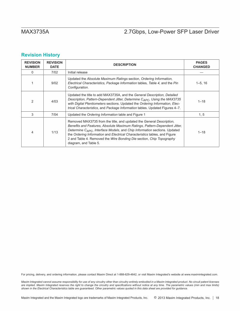
REVISION NUMBER
REVISION DATE DESCRIPTION PAGES
CHANGED0 7/02 Initial release —
1 9/02Updated the Absolute Maximum Ratings section, Ordering Information, Electrical Characteristics, Package Information tables, Table 4, and the Pin Configuration.
1–5, 16
2 4/03
Updated the title to add MAX3735A, and the General Description, Detailed Description, Pattern-Dependent Jitter, Determine CAPC, Using the MAX3735 with Digital Ptentiometers sections. Updated the Ordering Information, Elec-trical Characteristics, and Package Information tables. Updated Figures 4–7.
1–18
3 7/04 Updated the Ordering Information table and Figure 1 1, 5
4 1/13
Removed MAX3735 from the title, and updated the General Description, Benefits and Features, Absolute Maximum Ratings, Pattern-Dependent Jitter, Determine CAPC, Interface Models, and Chip Information sections. Updated the Ordering Information and Electrical Characteristics tables, and Figure 2 and Table 4. Removed the Wire Bonding Die section, Chip Topography diagram, and Table 5.
1–18
Maxim Integrated cannot assume responsibility for use of any circuitry other than circuitry entirely embodied in a Maxim Integrated product. No circuit patent licenses are implied. Maxim Integrated reserves the right to change the circuitry and specifications without notice at any time. The parametric values (min and max limits) shown in the Electrical Characteristics table are guaranteed. Other parametric values quoted in this data sheet are provided for guidance.
Maxim Integrated and the Maxim Integrated logo are trademarks of Maxim Integrated Products, Inc. © 2013 Maxim Integrated Products, Inc. 18
MAX3735A 2.7Gbps, Low-Power SFP Laser Driver
Revision History
For pricing, delivery, and ordering information, please contact Maxim Direct at 1-888-629-4642, or visit Maxim Integrated’s website at www.maximintegrated.com.