Embed Size (px)
Citation preview

General DescriptionThe MAX98307/MAX98308 fully differential mono Class DG multilevel power amplifiers with integrated inverting charge pumps offer highly efficient, high-power audio solutions for portable applications.Class DG multilevel modulation extends the dynamic range of the output signal by employing a charge-pump-generated negative rail as needed to extend the supply range. This scheme results in high efficiency over a wide output power range.The ICs combine Maxim’s active emissions limiting edge rate and overshoot control circuitry with multilevel output modulation to greatly reduce EMI. These features elimi-nate the need for output filtering as compared to tradition-al Class D devices, reducing component count and cost.The MAX98307’s 16-pin TQFN package features an adjustable gain set by external resistors. The MAX98308’s space-saving 12-bump WLP package features an inter-nally fixed gain of 8.5dB, 11.5dB, 14.5dB, 17.5dB, and 20.5dB set by a single gain input. Both devices operate over the extended -40°C to +85°C temperature range.
Applications
Benefits and Features High Efficiency Combined with High Output Power
• Class DG Multilevel Modulation Ensures Maximum Efficiency Over Wide Output Power Range
Improves Battery Life• Low 1.85mA Quiescent Current
High Output Power at 1% THD+N• 1.54W at VPVDD = 3.6V, 8Ω + 68μH Load• 2.85W at VPVDD = 5V, 8Ω + 68μH Load
High Output Power at 10% THD+N• 1.77W at VPVDD = 3.6V, 8Ω + 68μH Load• 3.3W at VPVDD = 5V, 8Ω + 68μH Load
84% Efficiency (VPVDD = 3.6V, at 500mW Output) Active Emissions Limiting and Class DG Multilevel
Output Modulation Eliminates EMI Output Filtering Requirement
Integrated Charge Pump and High Efficiency Results in Small Solution Size
Excellent RF Immunity Click-and-Pop Suppression Thermal and Overcurrent Protection Low-Current Shutdown Mode
Ordering Information appears at end of data sheet.
19-5848; Rev 6; 6/16
Cellular Phones Smartphones Notebook Computers
VoIP Phones Portable Audio Tablet PCs
PVDD
GND
FB-
FB+
IN-
IN+
SHDN PVSS
PGND
SVSSC1P
C1N
OUT+
OUT-
VCC
CHARGE PUMP
CLASS DGAMPLIFIER
MAX98307
PVDD
GND
IN-
IN+
SHDN PVSS
PGND
C1P
C1N
OUT+
OUT-
GAIN
CHARGE PUMP
CLASS DGAMPLIFIER
MAX98308
Simplified Block Diagrams
MAX98307/MAX98308 3.3W Mono Class DG Multilevel Audio Amplifier
EVALUATION KIT AVAILABLE

PVDD
GND
FB-
FB+
20kΩ
20kΩ
10kΩ0.33µF
0.33µF 10kΩ
12
1 713 3 1416
15
4
5
8
62
11
10
9
*SYSTEM BULK CAPACITOR
IN-
IN+
SHDN SVSS PVSS
PGND
C1P
C1N
OUT+
OUT-
N.C.
VCC
10µF* 10µF
4.7µF
0.1µF
2.6V TO 5.25
CHARGE PUMP
CLASS DGAMPLIFIER
MAX98307
0.1µF
PVDD
GND
GAIN B3
0.33µF
0.33µF
B2 A3 C1A1
B1
A4
B4
C4A2
C3
C2
*SYSTEM BULK CAPACITOR
IN-
IN+
SHDN PVSS
PGND
C1P
C1N
OUT+
OUT-
10µF* 10µF
4.7µF
0.1µF
2.6V TO 5.25
CHARGE PUMP
CLASS DGAMPLIFIER
MAX98308
MAX98307 Typical Application Circuit
MAX98308 Typical Application Circuit
MAX98307/MAX98308 3.3W Mono Class DG Multilevel Audio Amplifier
www.maximintegrated.com Maxim Integrated 2

PVDD to GND .........................................................-0.3V to +6VPGND to GND ......................................................-0.3V to +0.3VC1N to GND ......................................... (VPVSS - 0.3V) to +0.3VIN+, IN- (MAX98307) ................................ -0.3V to (VCC + 0.3V)VCC to PVDD (MAX98307) ..................................-0.3V to +0.3VPVSS to SVSS (MAX97307) ................................-0.3V to +0.3VPVSS, SVSS to GND (MAX98307) .........................-6V to +0.3VIN+, IN- (MAX98308) ...............................................-0.3V to +6VPVSS to GND (MAX98308) ....................................-6V to +0.3VAll Other Pins to GND .......................... -0.3V to (VPVDD + 0.3V)Continuous Current Into/Out of PVDD, VCC, PGND, GND,
OUT+, OUT-, C1P, C1N, PVSS, SVSS ......................±800mA
Continuous Current (all other pins) ..................................±20mADuration of OUT+/OUT- Short Circuit to PGND
or PVDD ................................................................ContinuousShort-Circuit Duration Between
OUT+ and OUT- Pins ............................................ContinuousContinuous Power Dissipation (TA = +70°C) for Multilayer Board TQFN (derate 20.8mW/°C above +70°C)..................1667mW WLP (derate 13.7mW/°C above +70°C) ....................1100mWJunction Temperature ......................................................+150°COperating Temperature Range ........................... -40°C to +85°CStorage Temperature Range ............................ -65°C to +150°CLead Temperature (soldering, 10s) (TQFN-EP) ..............+300°CSoldering Temperature (reflow) .......................................+260°C
TQFN Junction-to-Ambient Thermal Resistance (θJA) ..........48°C/W Junction-to-Case Thermal Resistance (θJC) ...............10°C/W
WLP Junction-to-Ambient Thermal Resistance (θJA) ..........73°C/W Junction-to-Case Thermal Resistance (θJC) ...............30°C/W
(Note 1)
(VPVDD = VCC = VSHDN = 3.6V, VPGND = VGND = 0V, ZL = 8Ω + 68µH between OUT+ and OUT-. [MAX98307 RIN+ = RIN- = 10kΩ, RFB+ = RFB- = 20kΩ] CIN+ = CIN- = 0.33µF, AV = 14.5dB, AC measurement bandwidth 20Hz to 20kHz, TA = TMIN to TMAX, unless otherwise noted. Typical values are at TA = +25°C.) (Notes 2, 3)
Note 1: Package thermal resistances were obtained using the method described in JEDEC specification JESD51-7, using a four-layer board. For detailed information on package thermal considerations, refer to www.maximintegrated.com/thermal-tutorial.
Absolute Maximum Ratings
Stresses beyond those listed under “Absolute Maximum Ratings” may cause permanent damage to the device. These are stress ratings only, and functional operation of the device at these or any other conditions beyond those indicated in the operational sections of the specifications is not implied. Exposure to absolute maximum rating conditions for extended periods may affect device reliability.
Package Thermal Characteristics
Electrical Characteristics
PARAMETER SYMBOL CONDITIONS MIN TYP MAX UNITS
Power-Supply Range VPVDD, VCC Guaranteed by PSRR test 2.6 5.25 V
Quiescent Current IDD VPVDD = 3.6V 1.85 2.7 mA
Shutdown Current ISHDN SHDN = GND 0.225 10 µA
Power-Supply Rejection Ratio (Note 4)
PSRR
VPVDD = 2.6V to 5.25V 78
dBf = 217Hz, 200mVP-P ripple 78
f = 10kHz, 200mVP-P ripple 67
Turn-On Time tON
Time from shutdown or power-on to full operation
MAX98308 25 40msMAX98307,
RIN = 10kΩ 50 80
Input DC Bias Voltage VBIAS 1.3 V
Input Resistance (MAX98308) RIN
AV = 20.5dB (maximum gain) 15 22
kΩ
AV = 17.5dB 22
AV = 14.5dB 22
AV = 11.5dB 28
AV = 8.5dB 40
MAX98307/MAX98308 3.3W Mono Class DG Multilevel Audio Amplifier
www.maximintegrated.com Maxim Integrated 3

(VPVDD = VCC = VSHDN = 3.6V, VPGND = VGND = 0V, ZL = 8Ω + 68µH between OUT+ and OUT-. [MAX98307 RIN+ = RIN- = 10kΩ, RFB+ = RFB- = 20kΩ] CIN+ = CIN- = 0.33µF, AV = 14.5dB, AC measurement bandwidth 20Hz to 20kHz, TA = TMIN to TMAX, unless otherwise noted. Typical values are at TA = +25°C.) (Notes 2, 3)
Electrical Characteristics (continued)
PARAMETER SYMBOL CONDITIONS MIN TYP MAX UNITS
Voltage Gain (MAX98308)
AV
GAIN = short to GND 20 20.5 21
dB
GAIN = 100kΩ pulldown to GND 17 17.5 18
GAIN = short to PVDD 14 14.5 15
GAIN = 100kΩ pullup to PVDD 11 11.5 12
GAIN = unconnected 8 8.5 9
Common-Mode Rejection Ratio (MAX98308)
CMRR fIN = 1kHz 65 dB
Output Power (MAX98307) POUT
fIN = 1kHz,THD+N = 1%
ZL = 8Ω + 68µH, VPVDD = 3.6V
1.54
W
ZL = 8Ω + 68µH, VPVDD = 4.2V
2
ZL = 8Ω + 68µH, VPVDD = 5.0V
2.85
fIN = 1kHz,THD+N = 10%
ZL = 8Ω + 68µH, VPVDD = 3.6V
1.77
ZL = 8Ω + 68µH, VPVDD = 4.2V
2.3
ZL = 8Ω + 68µH, VPVDD = 5.0V
3.3
Output Power (MAX98308) POUT
THD+N ≤ 1%
ZSPK = 8Ω + 68µH, VPVDD = 3.6V
1.4
W
ZSPK = 8Ω + 68µH, VPVDD = 4.2V
1.92
ZSPK = 8Ω + 68µH, VPVDD = 5.0V
2.7
THD+N ≤ 10%
ZSPK = 8Ω + 68µH, VPVDD = 3.6V
1.57
ZSPK = 8Ω + 68µH, VPVDD = 4.2V
2.13
MAX98307/MAX98308 3.3W Mono Class DG Multilevel Audio Amplifier
www.maximintegrated.com Maxim Integrated 4

(VPVDD = VCC = VSHDN = 3.6V, VPGND = VGND = 0V, ZL = 8Ω + 68µH between OUT+ and OUT-. [MAX98307 RIN+ = RIN- = 10kΩ, RFB+ = RFB- = 20kΩ] CIN+ = CIN- = 0.33µF, AV = 14.5dB, AC measurement bandwidth 20Hz to 20kHz, TA = TMIN to TMAX, unless otherwise noted. Typical values are at TA = +25°C.) (Notes 2, 3)
Note 2: 100% production tested at TA = +25°C. Specifications over temperature limits are guaranteed by design.Note 3: Testing performed with a resistive load in series with an inductor to simulate an actual speaker. For RL = 8Ω, L = 68µH.Note 4: Amplifier inputs AC-coupled to GND.Note 5: Specified at room temperature with an 8Ω resistive load in series with a 68µH inductive load connected across the BTL
outputs. Mode transitions controlled by SHDN active-low shutdown control.
Electrical Characteristics (continued)
PARAMETER SYMBOL CONDITIONS MIN TYP MAX UNITS
Total Harmonic Distortion Plus Noise
THD+N fIN = 1kHz, POUT = 1W 0.05 %
Output Offset Voltage VOS TA = +25°C ±1 ±5 mV
Click-and-Pop Level KCP
Peak voltage, A-weighted, 32 samples per second (Notes 4, 5)
Into shutdown -65dBV
Out of shutdown -65
Output Switching Frequency 340 kHz
Efficiency ηfIN = 1kHz, POUT at 500mW, THD+N = 0.02%
84%
fIN = 1kHz, POUT at 1W, THD+N = 0.05% 82
Current Limit ILIM 2 ARMS
Output Noise VN A-weighted 52 µVRMS
LOGIC INPUT (SHDN)
Input Voltage High VIH 1.4 V
Input Voltage Low VIL 0.4 V
Input Leakage Current TA = +25°C ±10 µA
MAX98307/MAX98308 3.3W Mono Class DG Multilevel Audio Amplifier
www.maximintegrated.com Maxim Integrated 5
(VPVDD = VCC = VSHDN = 3.6V, VPGND = VGND = 0V, ZL = 8Ω + 68µH between OUT+ and OUT-, AV = 14.5dB (MAX98307 RIN+ = RIN- = 10kΩ, RFB+ = RFB- = 20kΩ), CIN+ = CIN- = 0.33μF, AC measurement bandwidth 20Hz to 20kHz.)
Typical Operating Characteristics
TOTAL HARMONIC DISTORTION PLUSNOISE vs. OUTPUT POWER (MAX98307)
MAX
9830
7 to
c01
OUTPUT POWER (W)2.01.51.00.50 2.5
THD+
N (%
)
0.01
0.1
1
10
100
0.001
VPVDD = 3.6V
fIN = 1kHz
fIN = 100Hz
fIN = 6kHz
TOTAL HARMONIC DISTORTION PLUSNOISE vs. OUTPUT POWER (MAX98308)
MAX
9830
7 to
c04
OUTPUT POWER (W)2.01.51.00.50 2.5
THD+
N (%
)
0.01
0.1
1
10
100
0.001
VPVDD = 3.6V
fIN = 1kHz
fIN = 100Hz
fIN = 6kHz
TOTAL HARMONIC DISTORTION PLUSNOISE vs. OUTPUT POWER (MAX98307)
MAX
9830
7 to
c02
OUTPUT POWER (W)3.02.52.01.51.00.50 3.5
THD+
N (%
)
0.01
0.1
10
100
0.001
1
VPVDD = 4.2V
fIN = 1kHz
fIN = 100Hz
fIN = 6kHz
MAX
9830
7 to
c05
2.52.01.51.00.50 3.0
THD+
N (%
)
0.01
0.1
10
100
0.001
1
TOTAL HARMONIC DISTORTION PLUSNOISE vs. OUTPUT POWER (MAX98308)
VPVDD = 4.2V
fIN = 1kHz
fIN = 100Hz
fIN = 6kHz
OUTPUT POWER (W)
TOTAL HARMONIC DISTORTION PLUSNOISE vs. OUTPUT POWER (MAX98307)
MAX
9830
7 to
c03
OUTPUT POWER (W)43210 5
THD+
N (%
)
0.01
0.1
1
10
100
0.001
VPVDD = 5V
fIN = 1kHz
fIN = 100Hz
fIN = 6kHz
MAX
9830
7 to
c06
3.53.02.52.01.51.00.50 4.0
THD+
N (%
)
0.01
0.1
10
100
0.001
1
TOTAL HARMONIC DISTORTION PLUSNOISE vs. OUTPUT POWER (MAX98308)
VPVDD = 5V
fIN = 1kHz
fIN = 100Hz
fIN = 6kHz
OUTPUT POWER (W)
MAX98307/MAX98308 3.3W Mono Class DG Multilevel Audio Amplifier
Maxim Integrated 6www.maximintegrated.com
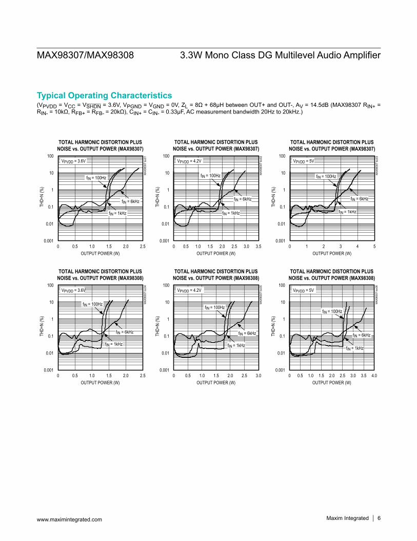
(VPVDD = VCC = VSHDN = 3.6V, VPGND = VGND = 0V, ZL = 8Ω + 68µH between OUT+ and OUT-, AV = 14.5dB (MAX98307 RIN+ = RIN- = 10kΩ, RFB+ = RFB- = 20kΩ), CIN+ = CIN- = 0.33μF, AC measurement bandwidth 20Hz to 20kHz.)
Typical Operating Characteristics (continued)
MAX
9830
7 to
c07
0.01
0.1
1
10
0.00110
TOTAL HARMONIC DISTORTION PLUSNOISE vs. FREQUENCY (MAX98307)
FREQUENCY (kHz)
THD+
N (%
)
10k1k100 100k
VPVDD = 3.6V
POUT = 300mW
POUT = 1.3W
MAX
9830
7 to
c10
0.01
0.1
1
10
0.00110
TOTAL HARMONIC DISTORTION PLUSNOISE vs. FREQUENCY (MAX98308)
FREQUENCY (kHz)
THD+
N (%
)
10k1k100 100k
VPVDD = 3.6V
POUT = 300mW
POUT = 1.1W
MAX
9830
7 to
c08
0.01
0.1
1
10
0.00110
TOTAL HARMONIC DISTORTION PLUSNOISE vs. FREQUENCY (MAX98307)
FREQUENCY (kHz)
THD+
N (%
)
10k1k100 100k
VPVDD = 4.2V
POUT = 500mW
POUT = 1.6W
MAX
9830
7 to
c11
0.01
0.1
1
10
0.00110
TOTAL HARMONIC DISTORTION PLUSNOISE vs. FREQUENCY (MAX98308)
FREQUENCY (kHz)
THD+
N (%
)
10k1k100 100k
VPVDD = 4.2V
POUT = 500mW
POUT = 1.6W
MAX
9830
7 to
c09
0.01
0.1
1
10
0.00110
TOTAL HARMONIC DISTORTION PLUSNOISE vs. FREQUENCY (MAX98307)
FREQUENCY (kHz)
THD+
N (%
)
10k1k100 100k
VPVDD = 5V
POUT = 700mW
POUT = 2.4W
MAX
9830
7 to
c12
0.01
0.1
1
10
0.00110
TOTAL HARMONIC DISTORTION PLUSNOISE vs. FREQUENCY (MAX98308)
FREQUENCY (kHz)
THD+
N (%
)
10k1k100 100k
VPVDD = 5V
POUT = 700mW
POUT = 2.4W
MAX98307/MAX98308 3.3W Mono Class DG Multilevel Audio Amplifier
Maxim Integrated 7www.maximintegrated.com

(VPVDD = VCC = VSHDN = 3.6V, VPGND = VGND = 0V, ZL = 8Ω + 68µH between OUT+ and OUT-, AV = 14.5dB (MAX98307 RIN+ = RIN- = 10kΩ, RFB+ = RFB- = 20kΩ), CIN+ = CIN- = 0.33μF, AC measurement bandwidth 20Hz to 20kHz.)
Typical Operating Characteristics (continued)
OUTPUT POWER vs. LOAD RESISTANCE(MAX98307)
MAX
9830
7 to
c13
LOAD RESISTANCE (Ω)
OUTP
UT P
OWER
(W)
10010
0.2
0.4
0.6
0.8
1.0
1.2
1.4
1.6
1.8
01 1k
VPVDD = 3.6VfIN = 1kHz
THD+N = 1%
THD+N = 10%
MAX
9830
7 to
c16
0.2
0.6
0.8
0
1.0
1.2
1.4
1.6
0
OUTP
UT P
OWER
(W)
LOAD RESISTANCE (Ω)100101 1k
VPVDD = 3.6VfIN = 1kHz
THD+N = 1%
THD+N = 10%
OUTPUT POWER vs. LOAD RESISTANCE(MAX98308)
OUTP
UT P
OWER
(W)
0.5
1.0
1.5
2.0
2.5
0
MAX
9830
7 to
c14
LOAD RESISTANCE (Ω)100101 1k
VPVDD = 4.2VfIN = 1kHz
THD+N = 1%
THD+N = 10%
OUTPUT POWER vs. LOAD RESISTANCE(MAX98307)
OUTPUT POWER vs. LOAD RESISTANCE(MAX98308)
LOAD RESISTANCE (Ω)
OUTP
UT P
OWER
(W)
10010
0.5
1.0
1.5
2.0
2.5
01 1k
THD+N = 10%
THD+N = 1%
MAX
9830
7 to
c17
VPVDD = 4.2VfIN = 1kHz
MAX
9830
7 to
c15
0.5
1.0
1.5
2.0
2.5
3.0
3.5
0
OUTP
UT P
OWER
(W)
LOAD RESISTANCE (Ω)100101 1k
VPVDD = 5VfIN = 1kHz
THD+N = 1%
THD+N = 10%
OUTPUT POWER vs. LOAD RESISTANCE(MAX98307)
OUTPUT POWER vs. LOAD RESISTANCE(MAX98308)
LOAD RESISTANCE (Ω)
OUTP
UT P
OWER
(mW
)
100101 1k
THD+N = 10%
THD+N = 1%
MAX
9830
7 to
c18
VPVDD = 5VfIN = 1kHz
0.5
1.0
1.5
2.0
2.5
3.0
3.5
0
MAX98307/MAX98308 3.3W Mono Class DG Multilevel Audio Amplifier
Maxim Integrated 8www.maximintegrated.com

(VPVDD = VCC = VSHDN = 3.6V, VPGND = VGND = 0V, ZL = 8Ω + 68µH between OUT+ and OUT-, AV = 14.5dB (MAX98307 RIN+ = RIN- = 10kΩ, RFB+ = RFB- = 20kΩ), CIN+ = CIN- = 0.33μF, AC measurement bandwidth 20Hz to 20kHz.)
Typical Operating Characteristics (continued)
OUTPUT POWER vs. SUPPLY VOLTAGE(MAX98307)
MAX
9830
7 to
c19
SUPPLY VOLTAGE (V)
OUTP
UT P
OWER
(W)
5.04.63.0 3.4 3.8 4.2
0.5
1.0
1.5
2.0
2.5
3.0
3.5
4.0
02.6 5.4
THD+N = 10%
THD+N = 1%
fIN = 1kHz
EFFICIENCY vs. OUTPUT POWER(MAX98307)
MAX
9830
7 to
c22
OUTPUT POWER (W)
EFFI
CIEN
CY (%
)
1.00.80.60.40.2
10
20
30
40
50
60
70
80
90
00 1.2
VPVDD = 3.6VfIN = 1kHz
OUTPUT POWER vs. SUPPLY VOLTAGE(MAX98308)
MAX
9830
7 to
c20
SUPPLY VOLTAGE (V)
OUTP
UT P
OWER
(W)
5.04.64.23.83.43.0
0.5
1.0
1.5
2.0
3.0
2.5
3.5
02.6 5.4
fIN = 1kHz
THD+N = 1%
THD+N = 10%
THERMALLY LIMITED
EFFICIENCY vs. OUTPUT POWER(MAX98307)
MAX
9830
7 to
c23
OUTPUT POWER (W)
EFFI
CIEN
CY (%
)
10
20
30
40
50
60
70
80
90
0
VPVDD = 4.2VfIN = 1kHz
1.41.20.8 1.00.4 0.60.20 1.6
GAIN vs. FREQUENCY(MAX98308)
MAX
9830
7 to
c21
FREQUENCY (kHz)
AMPL
ITUD
E (d
B)
10k1k100
-10
0
10
20
30
-2010 100k
GAIN = UNCONNECTEDGAIN = 100kΩ TO VPVDD
GAIN = PGND GAIN = VPVDDGAIN = 100kΩ TO PGND
EFFICIENCY vs. OUTPUT POWER(MAX98307)
MAX
9830
7 to
c24
OUTPUT POWER (W)
EFFI
CIEN
CY (%
)
10
20
30
40
50
60
70
80
90
0
VPVDD = 5VfIN = 1kHz
2.01.51.00.50 2.5
MAX98307/MAX98308 3.3W Mono Class DG Multilevel Audio Amplifier
Maxim Integrated 9www.maximintegrated.com

(VPVDD = VCC = VSHDN = 3.6V, VPGND = VGND = 0V, ZL = 8Ω + 68µH between OUT+ and OUT-, AV = 14.5dB (MAX98307 RIN+ = RIN- = 10kΩ, RFB+ = RFB- = 20kΩ), CIN+ = CIN- = 0.33μF, AC measurement bandwidth 20Hz to 20kHz.)
Typical Operating Characteristics (continued)
EFFICIENCY vs. OUTPUT POWER(MAX98308)
MAX
9830
7 to
c25
OUTPUT POWER (W)
EFFI
CIEN
CY (%
)
1.00.80.60.40.2
10
20
30
40
50
60
70
80
90
00 1.2
VPVDD = 3.6VfIN = 1kHz
SUPPLY CURRENT vs. SUPPLY VOLTAGE
MAX
9830
7 to
c28
SUPPLY VOLTAGE (V)
SUPP
LY C
URRE
NT (m
A)
5.04.54.03.53.0
0.5
1.0
1.5
2.0
2.5
3.0
02.5 5.5
VPVDD = 3.6VfIN = 1kHz
EFFICIENCY vs. OUTPUT POWER(MAX98308)
MAX
9830
7 to
c26
OUTPUT POWER (W)
EFFI
CIEN
CY (%
)
10
20
30
40
50
60
70
80
90
0
VPVDD = 4.2VfIN = 1kHz
1.41.20.8 1.00.4 0.60.20 1.6
SHUTDOWN CURRENTvs. SUPPLY VOLTAGE
MAX
9830
7 to
c29
SUPPLY VOLTAGE (V)
SHUT
DOW
N CU
RREN
T (n
A)
5.04.53.0 3.5 4.0
50
100
150
200
250
300
350
400
02.5 5.5
EFFICIENCY vs. OUTPUT POWER(MAX98308)
MAX
9830
7 to
c27
OUTPUT POWER (W)
EFFI
CIEN
CY (%
)
10
20
30
40
50
60
70
80
90
0
VPVDD = 5VfIN = 1kHz
2.01.51.00.50 2.5
POWER-SUPPLY REJECTION RATIO vs. FREQUENCY
MAX
9830
7 to
c30
FREQUENCY (Hz)
PSRR
(dB)
10k1k100
-80
-70
-60
-50
-40
-30
-20
-10
0
-9010 100k
VRIPPLE = 200mVP-P
MAX98307/MAX98308 3.3W Mono Class DG Multilevel Audio Amplifier
Maxim Integrated 10www.maximintegrated.com

(VPVDD = VCC = VSHDN = 3.6V, VPGND = VGND = 0V, ZL = 8Ω + 68µH between OUT+ and OUT-, AV = 14.5dB (MAX98307 RIN+ = RIN- = 10kΩ, RFB+ = RFB- = 20kΩ), CIN+ = CIN- = 0.33μF, AC measurement bandwidth 20Hz to 20kHz.)
Typical Operating Characteristics (continued)
STARTUP RESPONSEMAX98307 toc33
ISPEAKER100mA /div
20ms/div
VSHDN2V/div
SHUTDOWN RESPONSEMAX98307 toc34
ISPEAKER100mA /div
20ms/div
VSHDN2V/div
COMMON-MODE REJECTION RATIO vs. FREQUENCY (MAX98307)
MAX
9830
7 to
c31
FREQUENCY (Hz)
CMRR
(dB)
10k1k100
-80
-70
-60
-50
-40
-30
-20
-10
0
-9010 100k
fIN = 1kHz
COMMON-MODE REJECTION RATIO vs. FREQUENCY (MAX98308)
MAX
9830
7 to
c32
FREQUENCY (Hz)CM
RR (d
B)10k1k100
-70
-60
-50
-40
-30
-20
-10
0
-8010 100k
WIDEBAND vs. FREQUENCY
MAX
9830
7 to
c35
FREQUENCY (Hz)
OUTP
UT M
AGNI
TUDE
(dBV
)
10G1G
-160
-140
-120
-100
-80
-60
-40
-20
0
-180100k 100G
VPVDD = 3.6V
INBAND OUTPUT SPECTRUM
MAX
9830
7 to
c36
FREQUENCY (Hz)
OUTP
UT M
AGNI
TUDE
(dBV
)
10k1k100
-120
-100
-80
-60
-40
-20
0
-14010 100k
VPVDD = 3.6VCLIPPING WAVEFORM 10% THD+N
MAX98307 toc37
OUT-1V/div
200µs/div
OUT+1V/div
MAX98307/MAX98308 3.3W Mono Class DG Multilevel Audio Amplifier
Maxim Integrated 11www.maximintegrated.com

Pin/Bump Description
Pin/Bump Configurations
15
16
14
13
6
5
7
GND
OUT+
8
IN+
FB-
FB+
1 2
PVSS
4
12 11 9
C1N
C1P EP
N.C.
SVSS
PGND
OUT-+
PVDD
IN-
3
10
VCC
TQFN
MAX98307
TOP VIEW TOP VIEW(BUMPS SIDE DOWN)
WLP
PGNDPVSS
OUT-C1N
MAX98308
+1 2 3 4
A
IN+ IN-
GAINB
C
SHDN
SHDN
OUT+C1P GND PVDD
PIN BUMPNAME FUNCTION
MAX98307 MAX98308
1 B2 SHDN Active-Low Shutdown. Connect to GND for shutdown. Connect to PVDD for normal operation.
2 A2 GND Substrate and Signal Ground
3 A3 PVDD Power and Charge-Pump Supply. Bypass to PGND with a 0.1µF capacitor.
4 A4 OUT+ Positive Amplifier Output
5 B4 OUT- Negative Amplifier Output
6 C4 PGND Power Ground
7 — SVSS Amplifier Negative Power Supply. Connect to PVSS (MAX98307).
8 — N.C. No Connection. Not internally connected. Connect to GND or leave unconnected.
9 — FB- Negative Amplifier Feedback
10 C3 IN- Negative Amplifier Input
11 C2 IN+ Positive Amplifier Input
12 — FB+ Positive Amplifier Feedback
— B3 GAIN See Table 1 MAX98308 Gain Configuration for more information.
13 — VCC Signal Supply
14 C1 PVSS Charge-Pump Output. Connect a 10µF capacitor between PVSS and PGND.
15 B1 C1N Charge-Pump Flying Capacitor Negative Terminal. Connect a 4.7µF capacitor between C1N and C1P.
16 A1 C1P Charge-Pump Flying Capacitor Positive Terminal. Connect a 4.7µF capacitor between C1N and C1P.
— — EPExposed Pad (TQFN Only). Internally connected to GND. Connect to a large ground plane with multiple vias to maximize thermal performance. Not intended as an electrical connection point.
MAX98307/MAX98308 3.3W Mono Class DG Multilevel Audio Amplifier
www.maximintegrated.com Maxim Integrated 12

Detailed DescriptionThe MAX98307/MAX98308 fully differential mono Class DG multilevel power amplifiers with integrated inverting charge pumps offer highly efficient, high-power audio solutions for portable applications.The new Class DG multilevel modulation scheme extends the dynamic range of the output signal by employing a charge-pump-generated negative rail, which is used as needed to extend the supply range. When the negative rail is not needed, the output is drawn entirely from the standard supply. This scheme results in high efficiency over a wide output power range.The power amplifier incorporates active emissions limiting edge rate and overshoot control circuitry in combination with the multilevel output modulation scheme to greatly reduce EMI. These features eliminate the need for output filtering as compared to traditional Class D amplifiers, which reduces an application’s component count.The MAX98307 has an adjustable gain set by external resistors. The MAX98308 has preset fixed gains of 8.5dB, 11.5dB, 14.5dB, 17.5dB, and 20.5dB set by a gain select input (GAIN).
Class DG Multilevel OperationThe ICs’ filterless Class DG multilevel amplifiers feature a proprietary Maxim output stage that offers higher effi-ciency over a greater output power range than previous amplifiers. The amplifier combines Class D switching output efficiency and Class G supply level shifting with a multilevel output modulation scheme that with a 5V supply has efficiency better than 80% efficiency over the 0.35W to 2.2W output range.The Class DG multilevel output stage uses pulse-width modulation (PWM), a rail-to-rail digital output signal with variable duty cycle, to approximate an analog input signal as in a Class D amplifier. Rail-to-rail operation ensures that any dissipation at the output is due solely to the RDS(ON) of the power output MOSFETs. The Class DG multilevel output stage also senses the magnitude of the output signal and switches the supply rails as needed
to more efficiently supply the required signal power. For a low output signal swing requirement (below the bat-tery supply rail VPVDD), the output range is between VPVDD and ground. When output swing above VPVDD is required, VPVSS, an internal inverting charge-pump-generated negative rail replaces ground as the lower sup-ply. The high output swing range is then VPVDD to VPVSS, approximately double the low swing range. This approach efficiently manages power consumption by switching the operating rails as needed according to the output swing requirements. Additionally, multilevel output modulation is employed in to draw the maximum possible power from the lower impedance battery supply rail, VPVDD, rather than the higher impedance charge-pump-generated rail VPVSS. This is accomplished by generating PWM sig-nals that swing from ground to VPVDD or from ground to VPVSS at either end of the bridge tied load (BTL) rather than continually swinging from VPVDD to VPVSS. The sig-nals are modulated in such a way that VPVSS is used only as necessary to generate low-end signal swing.These combined operations ensure that power dissipation due to RDS(ON) loss and charge-pump impedance is min-imized, and that efficiency and output power is maximized across the audio range. Class DG multilevel operation is shown as Figure 1.
Figure 1. Class DG Multilevel Operation
MAX98307 fig01
400µs/div
OUT+5V/div
OUT-5V/div
OUT+ - OUT-10V/div
MAX98307/MAX98308 3.3W Mono Class DG Multilevel Audio Amplifier
www.maximintegrated.com Maxim Integrated 13

The Class DG multilevel efficiency compares favor-ably with Class AB and Class G amplifiers as shown in Figure 2. Note that efficiency at 1W is 85%.
EMI Filterless Output StageTraditional Class D amplifiers require the use of external LC filters, or shielding, to meet electromagnetic-interfer-ence (EMI) regulation standards. The active emissions limiting edge-rate control circuitry and Class DG multilevel modulation scheme reduce EMI emissions without the need for external filtering components, while maintaining high efficiency (see Figure 3).
Amplifier Current LimitIf the output current of the speaker amplifier exceeds the current limit, the ICs disable the outputs for approximately 100µs. After 100µs, the outputs are reenabled. If the fault condition still exists, the ICs continue to disable and reen-able the outputs until the fault condition is removed.
Figure 2. Class DG Multilevel vs. Typical Class G and Class AB Amplifier Efficiency
Figure 3. EMI Performance with VPVDD = 5V, 12in of Speaker Cable, No Output Filter
EFFICIENCY vs. OUTPUT POWER
OUTPUT POWER (W)
EFFI
CIEN
CY (%
)
1.81.61.2 1.40.4 0.6 0.8 1.00.2
10
20
30
40
50
60
70
80
90
00 2.0
MAX98307/MAX98308CLASS DG MULTILEVEL AMPLIFIER
CLASS AB AMPLIFIER
CLASS G AMPLIFIER
VPVDD = 5VfIN = 1kHz
1000-10
10
30
50
70
90
200 300 400 500
EN55022B LIMIT
HORIZONTAL
VERTICAL
600 700 800 900 1000FREQUENCY (MHz)
EMIS
SION
S LE
VEL (
dBµV
/m)
MAX98307/MAX98308 3.3W Mono Class DG Multilevel Audio Amplifier
www.maximintegrated.com Maxim Integrated 14

Click-and-Pop SuppressionThe speaker amplifier features Maxim’s comprehensive click-and-pop suppression. During startup, the click-and- pop suppression circuitry reduces any audible transient sources internal to the device. When entering shutdown, the differential speaker outputs quickly and simultane-ously ramp down to PGND.
Thermal and Short Circuit ProtectionThe ICs automatically enter thermal shutdown when the die temperature is greater than +160°C and reactivate at less than +135°C. Additionally, if the outputs are shorted to each other or either rail, the amplifier prevents cata-strophic loss by disabling the outputs.
ShutdownThe ICs feature a low-power shutdown mode, drawing less than 0.225µA (typ) supply current. Drive SHDN low to put the IC into the shutdown state.
Applications InformationFilterless Class DG OperationTraditional Class DG amplifiers require an output filter. The filter adds cost and size, as well as decreases effi-ciency and THD+N performance. The ICs’ active emis-sions limiting and Class DG multilevel output modulation allow for filterless operation while reducing external com-ponent count, and thereby, cost.Because the switching frequency of the ICs is well beyond the bandwidth of most speakers, voice coil movement due to the switching frequency is very small. Use a speaker with a series inductance > 10µH. Typical 8Ω speakers exhibit series inductances in the 20µH to 100µH range.
Differential Input AmplifierThe ICs feature a differential input configuration, making the device compatible with many codecs and offering improved noise immunity as compared to single-ended input amplifiers. In devices such as mobile phones, noisy digital signals can be picked up by an amplifier’s input traces. A differential amplifier amplifies the difference of the two inputs, while signals common to both inputs, such as switching noise, are rejected. While both ICs feature
differential amplifiers, their voltage gain is set in differing manners.The MAX98307 employs external feedback resistors as shown in Figure 4. Voltage gain of the input amplifier is set as:
( )FBV
IN
RA 20log dB 8.5dB
R
= +
where AV is the desired voltage gain in decibels. RIN+ should be equal to RIN-, and RFB+ should be equal to RFB-.In differential input configurations, the common-mode rejection ratio (CMRR) is primarily limited by the external resistor and capacitor matching. Ideally, to achieve the highest possible CMRR, the following external compo-nents should be selected where:
FB FB-
IN IN-
IN IN-
R RR R
andC C
+
+
+
=
=
The gain of the MAX98308 is selectable by connecting the gain-select bump GAIN as described in Table 1.
Figure 4. Setting the Voltage Gain of the MAX98307
CLASS DGOUTPUTSTAGE
FB+
IN+
IN-
FB-
RFB-
RFB+
RIN+
RIN-
MAX98307
MAX98307/MAX98308 3.3W Mono Class DG Multilevel Audio Amplifier
www.maximintegrated.com Maxim Integrated 15

Component SelectionPower-Supply Input (PVDD)PVDD powers the speaker amplifier and has a range of 2.6V to 5.25V. Bypass PVDD with 0.1µF and 10µF capacitors in parallel to PGND. Apply additional bulk capacitance at the device if long input traces between PVDD and the supply are used.
Input Coupling CapacitorsThe AC-coupling capacitors (CIN) and input resistors (RIN) form highpass filters that remove any DC bias from an input signal. See the MAX98307 Typical Application Circuit and MAX98308 Typical Application Circuit. CIN prevents any DC components from the input signal source appearing at the amplifier outputs. The -3dB point of the highpass filter, assuming zero source impedance due to the input signal source, is given by:
3 dBIN IN
1f2 R C
− =π × ×
Choose CIN so that f-3dB is well below the lowest frequen-cy of interest. Setting f-3dB too high affects the amplifier’s low-frequency response. Use capacitors with adequately low voltage coefficient (X5R or X7R recommended) for best low frequency THD+N performance.
Charge-Pump Capacitor SelectionUse capacitors with an equivalent series resistance (ESR) less than 50mΩ for optimum performance. Low-ESR ceramic capacitors minimize the output resistance of the charge pump. For best performance over the extended temperature range, select capacitors with an X7R dielec-tric and a rated voltage of at least 6.3V.
Charge-Pump Flying CapacitorThe value of the charge-pump flying capacitor affects the load regulation and output resistance of the charge pump. A charge-pump flying capacitor value that is too small (less than 1µF) degrades the amplifier’s ability to provide sufficient current drive. Increasing the value of this flying capacitor and decreasing the ESR improves load regula-tion and reduces the charge-pump output impedance, which improves the output power and efficiency of the amplifier. A 4.7µF or greater value, low-ESR capacitor is recommended.
Charge-Pump Hold CapacitorThe charge-pump hold capacitor value and ESR directly affect the ripple at the charge-pump rail, PVSS. Increasing the charge-pump hold capacitor value reduces output ripple. Likewise, decreasing the ESR of this capacitor reduces both ripple and output resistance. A 10µF or greater value, low-ESR capacitor is recommended.
Layout and GroundingProper layout and grounding are essential for optimum performance. Good grounding improves audio perfor-mance and prevents switching noise from coupling into the audio signal.Use wide, low-resistance output traces. As load imped-ance decreases, the current drawn from the device increases. At higher current, the resistance of the output traces decreases the power delivered to the load. For example, if 2W is delivered from the device output to an 8Ω load through 100mΩ of total speaker trace, 1.97W is delivered to the speaker. If power is delivered through 10mΩ of total speaker trace, 1.998W is delivered to the speaker. Wide output, supply, and ground traces also improve the power dissipation of the device.The ICs are inherently designed for excellent RF immu-nity. For best performance, add ground fills around all signal traces on top or bottom PCB planes.
Note: For both ICs, the Class DG output stage has a fixed gain of 8.5dB. Any gain or attenuation set by the external input stage resistors adds to or subtracts from this fixed gain.
Table 1. MAX98308 Gain ConfigurationGAIN PREAMPLIFIER GAIN (dB) OVERALL GAIN (dB)
Unconnected 0 8.5
100kΩ to VPVDD 3 11.5
Short to VPVDD 6 14.5
100kΩ to PGND 9 17.5
Short to PGND 12 20.5
MAX98307/MAX98308 3.3W Mono Class DG Multilevel Audio Amplifier
www.maximintegrated.com Maxim Integrated 16

Thermal ConsiderationsClass DG multilevel amplifiers provide much better effi-ciency and thermal performance than a comparable Class AB or Class G amplifier. However, the system’s thermal performance must be considered with realistic expecta-tions and include consideration of many parameters. This section examines Class DG multilevel amplifiers using general examples to illustrate good design practices.
MAX98307 (TQFN) Applications InformationThe exposed pad is the primary route of keeping heat away from the IC. With a bottom-side exposed pad, the PCB and its copper becomes the primary heatsink for the Class DG multilevel amplifier. Solder the exposed pad to a large copper polygon. Add as much copper as possible from this polygon to any adjacent pin on the amplifier as
well as to any adjacent components, provided these con-nections are at the same potential. These copper paths must be as wide as possible. Each of these paths con-tributes to the overall thermal capabilities of the system.The copper polygon to which the exposed pad is attached should have multiple vias to the opposite side of the PCB. Make this polygon as large as possible within the sys-tem’s constraints for signal routing.
MAX98308 (WLP) Applications InformationFor the latest application details on WLP construction, dimensions, tape carrier information, PCB techniques, bump-pad layout, and recommended reflow temperature profile, as well as the latest information on reliability test-ing results, refer to Application Note 1891: Wafer-Level Packaging (WLP) and Its Applications.
Note: All devices operate over the -40°C to +85°C temperature range.+Denotes a lead(Pb)-free/RoHS-compliant package./V denotes an automotive qualified part.*EP = Exposed pad.
Ordering InformationPART GAIN SET PIN-PACKAGE
MAX98307ETE+ External 16 TQFN-EP*
MAX98307ETE/V+ External 16 TQFN-EP*
MAX98308EWC+ Internal 12 WLP
MAX98307/MAX98308 3.3W Mono Class DG Multilevel Audio Amplifier
www.maximintegrated.com Maxim Integrated 17
Package InformationFor the latest package outline information and land patterns (footprints), go to www.maximintegrated.com/packages. Note that a “+”, “#”, or “-” in the package code indicates RoHS status only. Package drawings may show a different suffix character, but the drawing pertains to the package regardless of RoHS status.
PACKAGE TYPE PACKAGE CODE OUTLINE NO. LAND PATTERN NO.
16 TQFN-EP T1633+5 21-0136 90-0032
12 WLP W121A1+1 21-0542 Refer to Application Note 1891
MAX98307/MAX98308 3.3W Mono Class DG Multilevel Audio Amplifier
www.maximintegrated.com Maxim Integrated 18

Revision HistoryREVISION NUMBER
REVISION DATE DESCRIPTION PAGES
CHANGED
0 6/11 Initial release —
1 8/11 Updated output power conditions in the Electrical Characteristics table 4
2 9/11 Updated Electrical Characteristics table and TOC 20 2, 4, 8
3 9/11 Added EP to the Pin Description section and removed future product reference for the MAX98308 12, 17
4 3/12 Added RIN typical values for all gains and corrected error on TOCs 1–6 3, 6
5 3/15 Added MAX98307ETE/V+ to Ordering Information 17
6 6/16 Updated package code and outline number in Package Information table 18
Maxim Integrated cannot assume responsibility for use of any circuitry other than circuitry entirely embodied in a Maxim Integrated product. No circuit patent licenses are implied. Maxim Integrated reserves the right to change the circuitry and specifications without notice at any time. The parametric values (min and max limits) shown in the Electrical Characteristics table are guaranteed. Other parametric values quoted in this data sheet are provided for guidance.
Maxim Integrated and the Maxim Integrated logo are trademarks of Maxim Integrated Products, Inc.
MAX98307/MAX98308 3.3W Mono Class DG Multilevel Audio Amplifier
© 2014 Maxim Integrated Products, Inc. 19
For pricing, delivery, and ordering information, please contact Maxim Direct at 1-888-629-4642, or visit Maxim Integrated’s website at www.maximintegrated.com.