Embed Size (px)
Citation preview

General DescriptionThe MAX98357A/MAX98357B is an easy-to-use, low-cost, digital pulse-code modulation (PCM) input Class D ampli-fier that provides industry-leading Class AB audio perfor-mance with Class D efficiency. The digital audio interface automatically recognizes up to 35 different PCM and TDM clocking schemes which eliminates the need for I2C pro-gramming. Operation is further simplified by eliminating the need for an external MCLK signal that is typically used for PCM communication. Simply supply power, LRCLK, BCLK, and digital audio to generate audio! Furthermore, a novel pinout allows customers to use the cost-effective WLP package with no need for expensive vias (refer to Application Note 6643: Optimize Cost, Size, and Performance with MAX98357 WLP for more information).The digital audio interface is highly flexible with the MAX98357A supporting I2S data and the MAX98357B supporting left-justified data. Both ICs support 8 channel time division multiplexed (TDM) data. The digital audio interface accepts specified sample rates between 8kHz and 96kHz for all supported data formats. The ICs can be configured to produce a left channel, right channel, or (left/2 + right/2) output from the stereo input data. The ICs operate using 16/24/32-bit data for I2S and left-justified modes as well as 16-bit or 32-bit data using TDM mode. The ICs eliminate the need for the external MCLK signal that is typically used for PCM communication. This reduc-es EMI and possible board coupling issues in addition to reducing the size and pin count of the ICs.The ICs also feature a very high wideband jitter toler-ance (12ns typ) on BCLK and LRCLK to provide robust operation.Active emissions-limiting, edge-rate limiting, and over-shoot control circuitry greatly reduce EMI. A filterless spread-spectrum modulation scheme eliminates the need for output filtering found in traditional Class D devices and reduces the component count of the solution.The ICs are available in 9-pin WLP (1.345mm x 1.435mm x 0.64mm) and 16-pin TQFN (3mm x 3mm x 0.75mm) packages and are specified over the -40°C to +85°C tem-perature range.
Features Single-Supply Operation (2.5V to 5.5V) 3.2W Output Power into 4Ω at 5V 2.4mA Quiescent Current 92% Efficiency (RL = 8Ω, POUT = 1W) 22.8μVRMS Output Noise (AV = 15dB) Low 0.013% THD+N at 1kHz No MCLK Required Sample Rates of 8kHz to 96kHz Supports Left, Right, or (Left/2 + Right/2) Output Sophisticated Edge Rate Control Enables
Filterless Class D Outputs 77dB PSRR at 1kHz Low RF Susceptibility Rejects TDMA
Noise from GSM Radios Extensive Click-and-Pop Reduction Circuitry Robust Short-Circuit and Thermal Protection Available in Space-Saving Packages:
1.345mm x 1.435mm WLP (0.4mm Pitch) and 3mm x 3mm TQFN
Solution Size with Single Bypass Capacitor is 4.32mm2
Applications Single Li-ion Cell/5V Devices Smart Speakers Notebook Computers IoT Devices Gaming Devices (Audio and Haptics) Smartphones Tablets Cameras
19-6779; Rev 12; 4/19
Ordering Information appears at end of data sheet.
Functional Diagram appears at end of data sheet.
Simplified Block Diagram
DACCLASS DOUTPUTSTAGE
DIGITALAUDIO
INTERFACEPCM
INPUT
GAINCONTROL
SHUTDOWNAND
CHANNELSELECT
MAX98357AMAX98357B
MAX98357A/MAX98357B
Tiny, Low-Cost, PCM Class D Amplifier with Class AB Performance
Click here for production status of specific part numbers.
EVALUATION KIT AVAILABLE

TABLE OF CONTENTSGeneral Description . . . . . . . . . . . . . . . . . . . . . . . . . . . . . . . . . . . . . . . . . . . . . . . . . . . . . . . . . . . . . . . . . . . . . . . . . . . . 1Features . . . . . . . . . . . . . . . . . . . . . . . . . . . . . . . . . . . . . . . . . . . . . . . . . . . . . . . . . . . . . . . . . . . . . . . . . . . . . . . . . . . . . 1Applications . . . . . . . . . . . . . . . . . . . . . . . . . . . . . . . . . . . . . . . . . . . . . . . . . . . . . . . . . . . . . . . . . . . . . . . . . . . . . . . . . . 1Simplified Block Diagram. . . . . . . . . . . . . . . . . . . . . . . . . . . . . . . . . . . . . . . . . . . . . . . . . . . . . . . . . . . . . . . . . . . . . . . . 1Absolute Maximum Ratings . . . . . . . . . . . . . . . . . . . . . . . . . . . . . . . . . . . . . . . . . . . . . . . . . . . . . . . . . . . . . . . . . . . . . . 4Package Thermal Characteristics . . . . . . . . . . . . . . . . . . . . . . . . . . . . . . . . . . . . . . . . . . . . . . . . . . . . . . . . . . . . . . . . . 4Electrical Characteristics . . . . . . . . . . . . . . . . . . . . . . . . . . . . . . . . . . . . . . . . . . . . . . . . . . . . . . . . . . . . . . . . . . . . . . . . 4Typical Operating Characteristics . . . . . . . . . . . . . . . . . . . . . . . . . . . . . . . . . . . . . . . . . . . . . . . . . . . . . . . . . . . . . . . . . 9Pin Configurations . . . . . . . . . . . . . . . . . . . . . . . . . . . . . . . . . . . . . . . . . . . . . . . . . . . . . . . . . . . . . . . . . . . . . . . . . . . . 15Pin Description . . . . . . . . . . . . . . . . . . . . . . . . . . . . . . . . . . . . . . . . . . . . . . . . . . . . . . . . . . . . . . . . . . . . . . . . . . . . . . . 15Detailed Description. . . . . . . . . . . . . . . . . . . . . . . . . . . . . . . . . . . . . . . . . . . . . . . . . . . . . . . . . . . . . . . . . . . . . . . . . . . 16
Digital Audio Interface Modes. . . . . . . . . . . . . . . . . . . . . . . . . . . . . . . . . . . . . . . . . . . . . . . . . . . . . . . . . . . . . . . . . . 16MCLK Elimination . . . . . . . . . . . . . . . . . . . . . . . . . . . . . . . . . . . . . . . . . . . . . . . . . . . . . . . . . . . . . . . . . . . . . . . . 16BCLK Jitter Tolerance . . . . . . . . . . . . . . . . . . . . . . . . . . . . . . . . . . . . . . . . . . . . . . . . . . . . . . . . . . . . . . . . . . . . . 16BCLK Polarity. . . . . . . . . . . . . . . . . . . . . . . . . . . . . . . . . . . . . . . . . . . . . . . . . . . . . . . . . . . . . . . . . . . . . . . . . . . . 16LRCLK Polarity . . . . . . . . . . . . . . . . . . . . . . . . . . . . . . . . . . . . . . . . . . . . . . . . . . . . . . . . . . . . . . . . . . . . . . . . . . 16Standby Mode . . . . . . . . . . . . . . . . . . . . . . . . . . . . . . . . . . . . . . . . . . . . . . . . . . . . . . . . . . . . . . . . . . . . . . . . . . . 16
DAC Digital Filters. . . . . . . . . . . . . . . . . . . . . . . . . . . . . . . . . . . . . . . . . . . . . . . . . . . . . . . . . . . . . . . . . . . . . . . . . . . 17SD_MODE and Shutdown Operation. . . . . . . . . . . . . . . . . . . . . . . . . . . . . . . . . . . . . . . . . . . . . . . . . . . . . . . . . . . . . 17
Startup . . . . . . . . . . . . . . . . . . . . . . . . . . . . . . . . . . . . . . . . . . . . . . . . . . . . . . . . . . . . . . . . . . . . . . . . . . . . . . . . . 18I2S and Left Justified Mode . . . . . . . . . . . . . . . . . . . . . . . . . . . . . . . . . . . . . . . . . . . . . . . . . . . . . . . . . . . . . . . . . 19TDM Mode . . . . . . . . . . . . . . . . . . . . . . . . . . . . . . . . . . . . . . . . . . . . . . . . . . . . . . . . . . . . . . . . . . . . . . . . . . . . . . 19
Class D Speaker Amplifier . . . . . . . . . . . . . . . . . . . . . . . . . . . . . . . . . . . . . . . . . . . . . . . . . . . . . . . . . . . . . . . . . . . . 28Ultra-Low EMI Filterless Output Stage . . . . . . . . . . . . . . . . . . . . . . . . . . . . . . . . . . . . . . . . . . . . . . . . . . . . . . . . 28Speaker Current Limit . . . . . . . . . . . . . . . . . . . . . . . . . . . . . . . . . . . . . . . . . . . . . . . . . . . . . . . . . . . . . . . . . . . . . 28Gain Selection . . . . . . . . . . . . . . . . . . . . . . . . . . . . . . . . . . . . . . . . . . . . . . . . . . . . . . . . . . . . . . . . . . . . . . . . . . . 28Click-and-Pop Suppression . . . . . . . . . . . . . . . . . . . . . . . . . . . . . . . . . . . . . . . . . . . . . . . . . . . . . . . . . . . . . . . . . 28
Applications Information. . . . . . . . . . . . . . . . . . . . . . . . . . . . . . . . . . . . . . . . . . . . . . . . . . . . . . . . . . . . . . . . . . . . . . . . 29Filterless Class D Operation . . . . . . . . . . . . . . . . . . . . . . . . . . . . . . . . . . . . . . . . . . . . . . . . . . . . . . . . . . . . . . . . . . . 33Power-Supply Input . . . . . . . . . . . . . . . . . . . . . . . . . . . . . . . . . . . . . . . . . . . . . . . . . . . . . . . . . . . . . . . . . . . . . . . . . . 33Layout and Grounding. . . . . . . . . . . . . . . . . . . . . . . . . . . . . . . . . . . . . . . . . . . . . . . . . . . . . . . . . . . . . . . . . . . . . . . . 33
Functional Diagram . . . . . . . . . . . . . . . . . . . . . . . . . . . . . . . . . . . . . . . . . . . . . . . . . . . . . . . . . . . . . . . . . . . . . . . . . . . 33WLP Applications Information. . . . . . . . . . . . . . . . . . . . . . . . . . . . . . . . . . . . . . . . . . . . . . . . . . . . . . . . . . . . . . . . . . 34
Ordering Information . . . . . . . . . . . . . . . . . . . . . . . . . . . . . . . . . . . . . . . . . . . . . . . . . . . . . . . . . . . . . . . . . . . . . . . . . . 34Package Information . . . . . . . . . . . . . . . . . . . . . . . . . . . . . . . . . . . . . . . . . . . . . . . . . . . . . . . . . . . . . . . . . . . . . . . . . . 35Revision History . . . . . . . . . . . . . . . . . . . . . . . . . . . . . . . . . . . . . . . . . . . . . . . . . . . . . . . . . . . . . . . . . . . . . . . . . . . . . . 38
MAX98357A/MAX98357B
Tiny, Low-Cost, PCM Class D Amplifier with Class AB Performance
www.maximintegrated.com Maxim Integrated 2

LIST OF FIGURES
LIST OF TABLES
Figure 1. I2S Audio Interface Timing Diagram (MAX98357A) . . . . . . . . . . . . . . . . . . . . . . . . . . . . . . . . . . . . . . . . . . . . 8Figure 2. Left-Justified Audio Interface Timing Diagram (MAX98357B) . . . . . . . . . . . . . . . . . . . . . . . . . . . . . . . . . . . . 8Figure 3. TDM Audio Interface Timing Diagram . . . . . . . . . . . . . . . . . . . . . . . . . . . . . . . . . . . . . . . . . . . . . . . . . . . . . . 8Figure 4. SD_MODE Resistor Connected Using Open-Drain Driver . . . . . . . . . . . . . . . . . . . . . . . . . . . . . . . . . . . . . . 18Figure 5. SD_MODE Resistor Connected Using Push-Pull Driver . . . . . . . . . . . . . . . . . . . . . . . . . . . . . . . . . . . . . . . . 18Figure 6. Required startup sequence when using BCLK = 256kHz . . . . . . . . . . . . . . . . . . . . . . . . . . . . . . . . . . . . . . 19Figure 7. MAX98357A I2S Digital Audio Interface Timing, 16-Bit Resolution . . . . . . . . . . . . . . . . . . . . . . . . . . . . . . . 20Figure 8. MAX98357A I2S Digital Audio Interface Timing, 32-Bit Resolution . . . . . . . . . . . . . . . . . . . . . . . . . . . . . . . 21Figure 9. MAX98357B Left-Justified Digital Audio Interface Timing, 16-Bit Resolution . . . . . . . . . . . . . . . . . . . . . . . 22Figure 10. MAX98357B Left-Justified Digital Audio Interface Timing, 32-Bit Resolution . . . . . . . . . . . . . . . . . . . . . . 23Figure 11. MAX98357A TDM 16-Bit DAI Timing . . . . . . . . . . . . . . . . . . . . . . . . . . . . . . . . . . . . . . . . . . . . . . . . . . . . . 24Figure 12. MAX98357A TDM 32-Bit DAI Timing . . . . . . . . . . . . . . . . . . . . . . . . . . . . . . . . . . . . . . . . . . . . . . . . . . . . . 25Figure 13. MAX98357B TDM 16-Bit DAI Timing . . . . . . . . . . . . . . . . . . . . . . . . . . . . . . . . . . . . . . . . . . . . . . . . . . . . . 26Figure 14. MAX98357B TDM 32-Bit DAI Timing . . . . . . . . . . . . . . . . . . . . . . . . . . . . . . . . . . . . . . . . . . . . . . . . . . . . . 27Figure 15. EMI with 12in of Speaker Cable and No Output Filtering. . . . . . . . . . . . . . . . . . . . . . . . . . . . . . . . . . . . . . 28Figure 16. Left-Channel PCM Operation with 6dB Gain . . . . . . . . . . . . . . . . . . . . . . . . . . . . . . . . . . . . . . . . . . . . . . . 29Figure 17. Left-Channel PCM Operation with 12dB Gain . . . . . . . . . . . . . . . . . . . . . . . . . . . . . . . . . . . . . . . . . . . . . . 29Figure 18. Right-Channel PCM Operation with 6dB Gain . . . . . . . . . . . . . . . . . . . . . . . . . . . . . . . . . . . . . . . . . . . . . . 30Figure 19. (Left/2 + Right/2) PCM Operation with 6dB Gain. . . . . . . . . . . . . . . . . . . . . . . . . . . . . . . . . . . . . . . . . . . . 30Figure 20. Stereo PCM Operation Using Two ICs. . . . . . . . . . . . . . . . . . . . . . . . . . . . . . . . . . . . . . . . . . . . . . . . . . . . 31Figure 21. Channel TDM Operation (Gain Fixed at 12dB). . . . . . . . . . . . . . . . . . . . . . . . . . . . . . . . . . . . . . . . . . . . . . 32Figure 22. WLP Pin Connect for set 12dB Gain Without Via. . . . . . . . . . . . . . . . . . . . . . . . . . . . . . . . . . . . . . . . . . . . 34Figure 23. Example Layout Configured for Left-Channel Audio and Gain of 12dB. . . . . . . . . . . . . . . . . . . . . . . . . . . 34Figure 24. MAX98357A/MAX98357B WLP Ball Dimensions . . . . . . . . . . . . . . . . . . . . . . . . . . . . . . . . . . . . . . . . . . . 34
Table 1. RMS Jitter Tolerance . . . . . . . . . . . . . . . . . . . . . . . . . . . . . . . . . . . . . . . . . . . . . . . . . . . . . . . . . . . . . . . . . . . 16Table 2. BCLK Polarity . . . . . . . . . . . . . . . . . . . . . . . . . . . . . . . . . . . . . . . . . . . . . . . . . . . . . . . . . . . . . . . . . . . . . . . . . 16Table 3. LRCLK Polarity. . . . . . . . . . . . . . . . . . . . . . . . . . . . . . . . . . . . . . . . . . . . . . . . . . . . . . . . . . . . . . . . . . . . . . . . 16Table 4. Digital Filter Settings . . . . . . . . . . . . . . . . . . . . . . . . . . . . . . . . . . . . . . . . . . . . . . . . . . . . . . . . . . . . . . . . . . . 17Table 5. SD_MODE Control . . . . . . . . . . . . . . . . . . . . . . . . . . . . . . . . . . . . . . . . . . . . . . . . . . . . . . . . . . . . . . . . . . . . . 17Table 6. Examples of SD_MODE Pullup Resistor Values. . . . . . . . . . . . . . . . . . . . . . . . . . . . . . . . . . . . . . . . . . . . . . . 17Table 7. TDM Mode Channel Selection . . . . . . . . . . . . . . . . . . . . . . . . . . . . . . . . . . . . . . . . . . . . . . . . . . . . . . . . . . . . 20Table 8. Gain Selection . . . . . . . . . . . . . . . . . . . . . . . . . . . . . . . . . . . . . . . . . . . . . . . . . . . . . . . . . . . . . . . . . . . . . . . . 28
MAX98357A/MAX98357B
Tiny, Low-Cost, PCM Class D Amplifier with Class AB Performance
www.maximintegrated.com Maxim Integrated 3

(Note 1)
VDD, LRCLK, BCLK, and DIN to GND ....................-0.3V to +6VAll Other Pins to GND .............................. -0.3V to (VDD + 0.3V)Continuous Current In/Out of VDD/GND/OUT_..................±1.6AContinuous Input Current (all other pins) .........................±20mADuration of OUT_ Short Circuit to GND or VDD….. ..ContinuousDuration of OUTP Short to OUTN .............................Continuous
Continuous Power Dissipation (TA = +70°C) WLP (derate 13.7mW/°C above +70°C) ....................1096mW TQFN (derate 20.8mW/°C above +70°C)..................1666mW
Junction Temperature ......................................................+150°COperating Temperature Range ........................... -40°C to +85°CStorage Temperature Range ............................ -65°C to +150°CSoldering Temperature (reflow) .......................................+260°CLead Temperature (soldering, 10s, TQFN) .....................+300°C
WLP Junction-to-Ambient Thermal Resistance (θJA) ..........73°C/W Junction-to-Case Thermal Resistance (θJC) ...............50°C/W
TQFN Junction-to-Ambient Thermal Resistance (θJA) ..........48°C/W Junction-to-Case Thermal Resistance (θJC) .................7°C/W
(VDD = 5V, VGND = 0V, GAIN_SLOT = VDD. BCLK = 3.072MHz, LRCLK = 48kHz, speaker loads (ZSPK) connected between OUTP and OUTN, ZSPK = ∞, TA = TMIN to TMAX, unless otherwise noted. Typical values are at TA = +25°C.) (Note 2)
PARAMETER SYMBOL CONDITIONS MIN TYP MAX UNITSSupply Voltage Range VDD Guaranteed by PSSR test 2.5 5.5 VUndervoltage Lockout UVLO 1.5 1.8 2.3 V
Quiescent Current IDDTA = +25°C 2.75 3.35
mATA = +25°C, VDD = 3.7V 2.4 2.85
Shutdown Current ISHDN SD_MODE = 0V, TA = +25°C 0.6 2 µAStandby Current ISTNDBY SD_MODE = 1.8V, no BCLK, TA = +25°C 340 400 µA
Turn-On Time tON 7 7.5 ms
Output Offset Voltage VOS TA = +25°C, gain = 15dB ±0.3 ±2.5 mV
Click-and-Pop Level KCP
Peak voltage, TA = +25°C, A-weighted, 32 samples per second (Note 3)
Into shutdown -72dBV
Out of shutdown -66
Power-Supply Rejection Ratio PSRR
VDD = 2.5V to 5.5V, TA = +25°C 60 75
dBTA = +25°C(Notes 3, 4)
f = 217Hz,200mVP-P ripple 77
f = 10kHz,200mVP-P ripple 60
Absolute Maximum Ratings
Stresses beyond those listed under “Absolute Maximum Ratings” may cause permanent damage to the device. These are stress ratings only, and functional operation of the device at these or any other conditions beyond those indicated in the operational sections of the specifications is not implied. Exposure to absolute maximum rating conditions for extended periods may affect device reliability.
Electrical Characteristics
Note 1: Package thermal resistances were obtained using the method described in JEDEC specification JESD51-7, using a four-layer board. For detailed information on package thermal considerations, refer to www.maximintegrated.com/thermal-tutorial.
Package Thermal Characteristics
MAX98357A/MAX98357B
Tiny, Low-Cost, PCM Class D Amplifier with Class AB Performance
www.maximintegrated.com Maxim Integrated 4

(VDD = 5V, VGND = 0V, GAIN_SLOT = VDD. BCLK = 3.072MHz, LRCLK = 48kHz, speaker loads (ZSPK) connected between OUTP and OUTN, ZSPK = ∞, TA = TMIN to TMAX, unless otherwise noted. Typical values are at TA = +25°C.) (Note 2)
PARAMETER SYMBOL CONDITIONS MIN TYP MAX UNITS
Output Power (Note 3) POUT
THD+N 10%, gain = 12dB
ZSPK = 4Ω + 33µH 3.2
W
ZSPK = 8Ω + 68µH 1.8ZSPK = 8Ω + 68µH,VDD = 3.7V 0.93
THD+N = 1%, gain = 12dB
ZSPK = 4Ω + 33µH 2.5ZSPK = 8Ω + 68µH 1.4ZSPK = 8Ω + 68µH,VDD = 3.7V 0.77
Total Harmonic Distortion + Noise THD+N
f = 1kHz, POUT = 1W, TA = +25°C,ZSPK = 4Ω + 33µH, WLP 0.02 0.06
%f = 1kHz, POUT = 1W, TA = +25°C,ZSPK = 4Ω + 33µH, TQFN 0.02
f = 1kHz, POUT = 0.5W, TA = +25°C,ZSPK = 8Ω + 68µH 0.013
Dynamic Range DR A-weighted, ZSPK = 8Ω + 33µH, VRMS = 3.40V, 24- or 32-bit data 103.5 dB
Output Noise VN A-weighted, 24- or 32-bit data (Note 4) 22.8 µVRMS
Gain (Relative to a 2.1dBV Reference Level) AV
GAIN_SLOT = GND through 100kΩ 14.4 15 15.6
dBGAIN_SLOT = GND 11.4 12 12.6GAIN_SLOT = unconnected 8.4 9 9.6GAIN_SLOT = VDD 5.4 6 6.6GAIN_SLOT = VDD through 100kΩ 2.4 3 3.6
Current Limit ILIM 2.8 A
Efficiency ε ZSPK = 8Ω + 68µH, THD+N = 10%,f = 1kHz, gain = 12dB 92 %
DAC Gain Error 1 %Frequency Response -0.2 +0.2 dBClass D Switching Frequency fOSC 300 kHzSpread-Spectrum Bandwidth ±20 kHzDAC DIGITAL FILTERSVOICE MODE IIR LOWPASS FILTER (LRCLK < 30kHz)
Passband Cutoff fPLP
Ripple limit cutoff 0.443 x fS Hz
-3dB cutoff 0.446 x fS
Stopband Cutoff fSLP0.464 x fS
Hz
Stopband Attenuation f > fSLP 75 dB
Electrical Characteristics (continued)
MAX98357A/MAX98357B
Tiny, Low-Cost, PCM Class D Amplifier with Class AB Performance
www.maximintegrated.com Maxim Integrated 5
(VDD = 5V, VGND = 0V, GAIN_SLOT = VDD. BCLK = 3.072MHz, LRCLK = 48kHz, speaker loads (ZSPK) connected between OUTP and OUTN, ZSPK = ∞, TA = TMIN to TMAX, unless otherwise noted. Typical values are at TA = +25°C.) (Note 2)
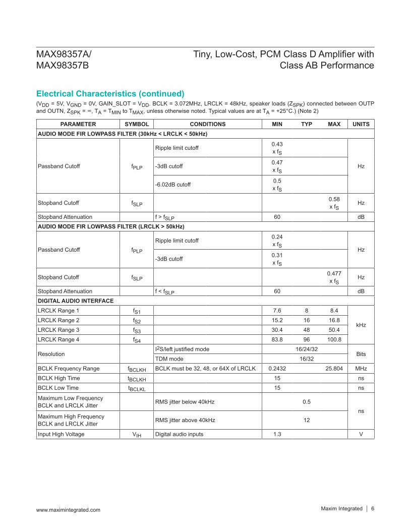
PARAMETER SYMBOL CONDITIONS MIN TYP MAX UNITSAUDIO MODE FIR LOWPASS FILTER (30kHz < LRCLK < 50kHz)
Passband Cutoff fPLP
Ripple limit cutoff 0.43 x fS
Hz-3dB cutoff 0.47 x fS
-6.02dB cutoff 0.5 x fS
Stopband Cutoff fSLP0.58 x fS
Hz
Stopband Attenuation f > fSLP 60 dBAUDIO MODE FIR LOWPASS FILTER (LRCLK > 50kHz)
Passband Cutoff fPLP
Ripple limit cutoff 0.24 x fS
Hz-3dB cutoff 0.31
x fS
Stopband Cutoff fSLP0.477 x fS
Hz
Stopband Attenuation f < fSLP 60 dBDIGITAL AUDIO INTERFACELRCLK Range 1 fS1 7.6 8 8.4
kHzLRCLK Range 2 fS2 15.2 16 16.8LRCLK Range 3 fS3 30.4 48 50.4LRCLK Range 4 fS4 83.8 96 100.8
ResolutionI2S/left justified mode 16/24/32
BitsTDM mode 16/32
BCLK Frequency Range fBCLKH BCLK must be 32, 48, or 64X of LRCLK 0.2432 25.804 MHzBCLK High Time tBCLKH 15 nsBCLK Low Time tBCLKL 15 ns
Maximum Low Frequency BCLK and LRCLK Jitter RMS jitter below 40kHz 0.5
nsMaximum High Frequency BCLK and LRCLK Jitter RMS jitter above 40kHz 12
Input High Voltage VIH Digital audio inputs 1.3 V
Electrical Characteristics (continued)
MAX98357A/MAX98357B
Tiny, Low-Cost, PCM Class D Amplifier with Class AB Performance
www.maximintegrated.com Maxim Integrated 6

Note 2: 100% production tested at TA = +25°C. Specifications over temperature limits are guaranteed by design.Note 3: Class D amplifier testing performed with a resistive load in series with an inductor to simulate an actual speaker load. For
RL = 8Ω, LL = 68µH. For RL = 4Ω, LL = 33µH.Note 4: Digital silence used for input signal.Note 5: Dynamic range measured using the EIAJ method. -60dBFS 1kHz output signal, A-weighted, and normalized to 0dBFS.
f = 20Hz to 20kHz.
(VDD = 5V, VGND = 0V, GAIN_SLOT = VDD. BCLK = 3.072MHz, LRCLK = 48kHz, speaker loads (ZSPK) connected between OUTP and OUTN, ZSPK = ∞, TA = TMIN to TMAX, unless otherwise noted. Typical values are at TA = +25°C.) (Note 2)
PARAMETER SYMBOL CONDITIONS MIN TYP MAX UNITSInput Low Voltage VIL Digital audio inputs 0.6 VInput Leakage Current IIH, IIL VIN = 0V, VDD = 5.5V, TA = +25°C -1 +1 µAInput Capacitance CIN 3 pFDIN to BCLK Setup Time tSETUP 10 nsLRCLK to BCLK Setup Time tSYNCSET 10 nsDIN to BCLK Hold Time tHOLD 10 nsLRCLK to BCLK Hold Time tSYNCHOLD 10 nsSD_MODE COMPARATOR TRIP POINTSB0
See SD_MODE and shutdown operation for details
0.08 0.16 0.355VB1 0.65 0.77 0.825
B2 1.245 1.4 1.5SD_MODE Pulldown Resistor RPD 92 100 108 kΩGAIN COMPARATOR TRIP POINTS
V_GAIN_SLOT
AV = 3dB gain 0.65 x VDD
0.85 x VDD
V
AV = 6dB gain 0.9 x VDD
VDD
AV = 9dB gain 0.4 x VDD
0.6 x VDD
AV = 12dB gain 0 0.1 x VDD
AV = 15dB gain 0.15 x VDD
0.35 x VDD
Electrical Characteristics (continued)
MAX98357A/MAX98357B
Tiny, Low-Cost, PCM Class D Amplifier with Class AB Performance
www.maximintegrated.com Maxim Integrated 7
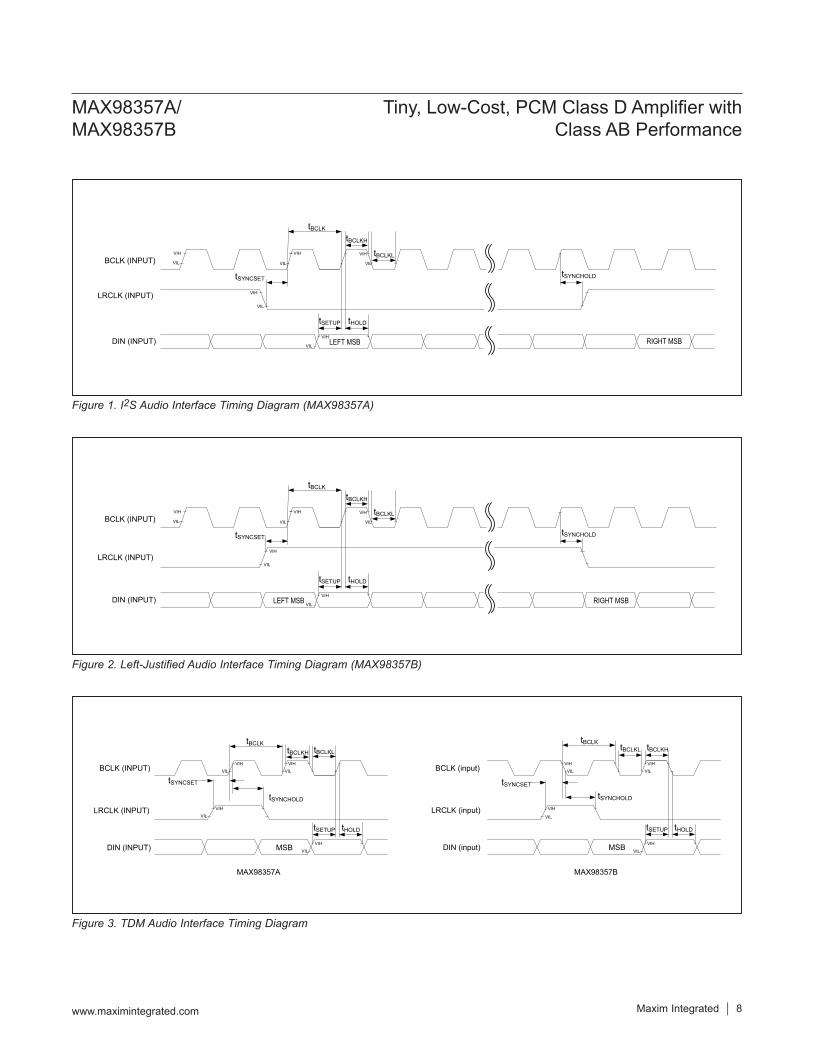
Figure 1. I2S Audio Interface Timing Diagram (MAX98357A)
Figure 3. TDM Audio Interface Timing Diagram
Figure 2. Left-Justified Audio Interface Timing Diagram (MAX98357B)
LRCLK (INPUT)
BCLK (INPUT)
DIN (INPUT) LEFT MSB
tHOLDtSETUP
tBCLKH
tBCLKL
tBCLK
tSYNCSET
RIGHT MSB
tSYNCHOLD
VIH
VIL
VIH
VIL
VIH
VIH
VIL VIL
VIH
VIL
LRCLK (INPUT)
BCLK (INPUT)
DIN (INPUT)
tHOLDtSETUP
tSYNCHOLD
MSB
tBCLKH tBCLKL
tBCLK
tSYNCSET
LRCLK (input)
BCLK (input)
DIN (input)
tHOLDtSETUP
tSYNCHOLD
MSB
tBCLKL tBCLKHtBCLK
tSYNCSET
MAX98357A MAX98357B
VILVIH
VILVIH
VILVIH
VILVIH
VILVIH
VIH
VIL
VIL
VIH
VIHVIL
LRCLK (INPUT)
BCLK (INPUT)
DIN (INPUT) LEFT MSB
tHOLDtSETUP
tBCLKH
tBCLKL
tBCLK
tSYNCSET tSYNCHOLD
VIH
VIL
VIH
VIL
VIH
VIH
VIL VIL
VIH
VIL RIGHT MSB
MAX98357A/MAX98357B
Tiny, Low-Cost, PCM Class D Amplifier with Class AB Performance
www.maximintegrated.com Maxim Integrated 8

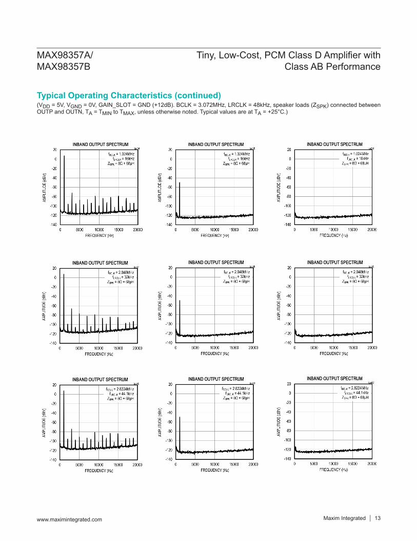
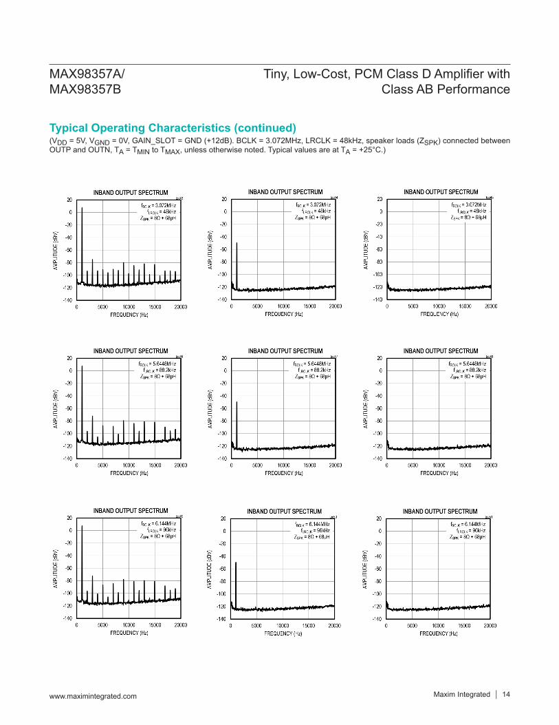
(VDD = 5V, VGND = 0V, GAIN_SLOT = GND (+12dB). BCLK = 3.072MHz, LRCLK = 48kHz, speaker loads (ZSPK) connected between OUTP and OUTN, TA = TMIN to TMAX, unless otherwise noted. Typical values are at TA = +25°C.)
Typical Operating Characteristics
0.0
0.5
1.0
1.5
2.0
2.5
3.0
3.5
4.0
2.5 3.0 3.5 4.0 4.5 5.0 5.5
QUIE
CENT
CUR
RENT
(mA)
SUPPLY VOLTAGE (V)
QUIESCENT CURRENT vs. SUPPLY VOLTAGE
VDDIO = 1.8Vtoc01
0.0
0.1
0.2
0.3
0.4
0.5
0.6
0.7
0.8
0.9
1.0
2.5 3.0 3.5 4.0 4.5 5.0 5.5SH
UTDO
WN
CURR
ENT
(µA)
SUPPLY VOLTAGE (V)
SHUTDOWN CURRENT vs. SUPPLY VOLTAGEtoc02
VDDIO = 1.8V
MAX98357A/MAX98357B
Tiny, Low-Cost, PCM Class D Amplifier with Class AB Performance
Maxim Integrated 9www.maximintegrated.com
(VDD = 5V, VGND = 0V, GAIN_SLOT = GND (+12dB). BCLK = 3.072MHz, LRCLK = 48kHz, speaker loads (ZSPK) connected between OUTP and OUTN, TA = TMIN to TMAX, unless otherwise noted. Typical values are at TA = +25°C.)
Typical Operating Characteristics (continued)
0.0
0.5
1.0
1.5
2.0
2.5
1 10 100
OUTP
UT P
OWER
(W)
LOAD RESISTANCE
OUTPUT POWER vs. LOAD RESISTANCE
VDD = 3.7V
10% THD+N
1% THD+N
toc15
0.0
0.5
1.0
1.5
2.0
2.5
3.0
3.5
1 10 100
OUTP
UT P
OWER
(W)
LOAD RESISTANCE
OUTPUT POWER vs. LOAD RESISTANCE
VDD = 4.2V
10% THD+N
1% THD+N
toc16
0.0
0.5
1.0
1.5
2.0
2.5
3.0
3.5
4.0
4.5
1 10 100
OUTP
UT P
OWER
(W)
LOAD RESISTANCE
OUTPUT POWER vs. LOAD RESISTANCE
VDD = 5V
10% THD+N
1% THD+N
toc17
MAX98357A/MAX98357B
Tiny, Low-Cost, PCM Class D Amplifier with Class AB Performance
Maxim Integrated 10www.maximintegrated.com
(VDD = 5V, VGND = 0V, GAIN_SLOT = GND (+12dB). BCLK = 3.072MHz, LRCLK = 48kHz, speaker loads (ZSPK) connected between OUTP and OUTN, TA = TMIN to TMAX, unless otherwise noted. Typical values are at TA = +25°C.)
Typical Operating Characteristics (continued)
-3.0
-2.5
-2.0
-1.5
-1.0
-0.5
0.0
0.5
1.0
1 10 100 1000 10000 100000
NORM
ALIZE
D GA
IN (d
B)
FREQUENCY (Hz)
NORMALIZED GAIN vs. FREQUENCYtoc20
MAX98357A/MAX98357B
Tiny, Low-Cost, PCM Class D Amplifier with Class AB Performance
Maxim Integrated 11www.maximintegrated.com

(VDD = 5V, VGND = 0V, GAIN_SLOT = GND (+12dB). BCLK = 3.072MHz, LRCLK = 48kHz, speaker loads (ZSPK) connected between OUTP and OUTN, TA = TMIN to TMAX, unless otherwise noted. Typical values are at TA = +25°C.)
Typical Operating Characteristics (continued)
0
10
20
30
40
50
60
70
80
90
100
10 100 1000 10000 100000
PSRR
(dB)
FREQUENCY (Hz)
POWER-SUPPLY REJECTION RATIOvs. FREQUENCY
toc27
0
10
20
30
40
50
60
70
80
90
100
2.5 3.0 3.5 4.0 4.5 5.0 5.5
PSRR
(dB)
SUPPLY VOLTAGE (V)
POWER-SUPPLY REJECTION RATIOvs. SUPPLY VOLTAGE
fS = 1kHz
toc28TURN-ON RESPONSE
OUTPUT1V/div
SD_MODE1V/div
toc29
2ms/div
TURN-OFF RESPONSE
OUTPUT1V/div
SD_MODE1V/div
toc30
1ms/div
BCLK2V/div
LRCLK2V/div
OUTPUT1V/div
toc30a
500µs/div
TURN-OFF RESPONSE(STANDBY MODE)
BCLK2V/div
LRCLK2V/div
OUTPUT1V/div
toc30b
2ms/div
TURN-ON RESPONSE(STANDBY MODE)
MAX98357A/MAX98357B
Tiny, Low-Cost, PCM Class D Amplifier with Class AB Performance
Maxim Integrated 12www.maximintegrated.com
(VDD = 5V, VGND = 0V, GAIN_SLOT = GND (+12dB). BCLK = 3.072MHz, LRCLK = 48kHz, speaker loads (ZSPK) connected between OUTP and OUTN, TA = TMIN to TMAX, unless otherwise noted. Typical values are at TA = +25°C.)
Typical Operating Characteristics (continued)
MAX98357A/MAX98357B
Tiny, Low-Cost, PCM Class D Amplifier with Class AB Performance
Maxim Integrated 13www.maximintegrated.com
(VDD = 5V, VGND = 0V, GAIN_SLOT = GND (+12dB). BCLK = 3.072MHz, LRCLK = 48kHz, speaker loads (ZSPK) connected between OUTP and OUTN, TA = TMIN to TMAX, unless otherwise noted. Typical values are at TA = +25°C.)
Typical Operating Characteristics (continued)
MAX98357A/MAX98357B
Tiny, Low-Cost, PCM Class D Amplifier with Class AB Performance
Maxim Integrated 14www.maximintegrated.com

PINNAME FUNCTION
WLP TQFN
A1 4 SD_MODEShutdown and Channel Select. Pull SD_MODE low to place the device in shutdown. In I2Sor LJ mode, SD_MODE selects the data channel (Table 5). In TDM mode, SD_MODE andGAIN_SLOT are both used for channel selection (Table 7).
A2 7, 8 VDD Power-Supply InputA3 9 OUTP Positive Speaker Amplifier OutputB1 1 DIN Digital Input Signal
B2 2 GAIN_SLOT
Gain and Channel Selection. In I2S and LJ mode determines amplifier output gain (Table 8)In TDM mode, used for channel selection with SD_MODE (Table 7). In TDM mode, gain isfixed at 12dB.
B3 10 OUTN Negative Speaker Amplifier OutputC1 16 BCLK Bit Clock InputC2 3, 11, 15 GND GroundC3 14 LRCLK Frame Clock. Left/right clock for I2S and LJ mode. Sync clock for TDM mode.
— 5, 6, 12, 13 N.C. No Connection
— — EP Exposed Pad. The exposed pad is not internally connected. Connect the exposed page to asolid ground plane for thermal dissipation.
Pin Description
Pin Configurations
WLP
TOP VIEWBUMP SIDE DOWN
GNDBCLK LRCLK
GAIN_SLOTDIN OUTN
VDDSD_MODE OUTP
MAX98357AMAX98357B
+
A1
B1
C1 C2 C3
B2 B3
A3A2
15
16
14
13
5
6
7
GND
SD_M
ODE
8
DIN
OUTN
OUTP
N.C.
1 3
LRCLK
4
12 10 9
GND
BCLK
VDD
VDD
N.C.
N.C.
GAIN
_SLO
TGN
D
2
11
N.C.
TQFN
MAX98357AMAX98357B
TOP VIEW
+
MAX98357A/MAX98357B
Tiny, Low-Cost, PCM Class D Amplifier with Class AB Performance
www.maximintegrated.com Maxim Integrated 15

Detailed DescriptionThe MAX98357A/MAX98357B are digital PCM input Class D power amplifiers. The MAX98357A accepts stan-dard I2S data through DIN, BCLK, and LRCLK while the MAX98357B accepts left-justified data through the same inputs. Both versions also accept 16-bit or 32-bit TDM data with up to eight slots. The digital audio interface eliminates the need for an external MCLK signal that is typically required for I2S data transmission.SD_MODE selects which data word is output by the amplifier and is used to put the ICs into shutdown. These devices offer five gain settings in I2S/left-justified mode and a fixed 12dB gain in TDM mode. Channel selection in TDM mode is set with the combination of SD_MODE and GAIN_SLOT (Table 7).The MAX98357A/MAX98357B DAI includes a DC blocker with a -3dB cutoff at 3.7Hz.The MAX98357A/MAX98357B feature low-quiescent cur-rent, comprehensive click-and-pop suppression, and excellent RF immunity. The ICs offer Class AB audio performance with Class D efficiency in a minimal board-space solution. The Class D amplifier features spread-spectrum modulation with edge-rate and overshoot con-trol circuitry that offers significant improvements in switch-mode amplifier radiated emissions. The amplifier features click-and-pop suppression that reduces audible transients on startup and shutdown. The amplifier includes thermal-overload and short-circuit protection.
Digital Audio Interface ModesThe input stage of the digital audio interface is highly flexi-ble, supporting 8kHz–96kHz sampling rates with 16/24/32-bit resolution for I2S/left justified data as well as up to a 8-slot, 16-bit or 32-bit time division multiplexed (TDM) format. When LRCLK has a 50% duty cycle the data format is determined by the part number selection (MAX98357A/MAX98357B). When a frame sync pulse is used for the LRCLK the data format is automatically configured in TDM mode. The frame sync pulse indicates the beginning of the first time slot.
MCLK EliminationThe ICs eliminate the need for the external MCLK signal that is typically used for PCM communication. This reduces EMI and possible board coupling issues in addition to reducing the size and pin-count of the ICs.
BCLK Jitter ToleranceThe ICs feature a BCLK jitter tolerance of 0.5ns for RMS jitter below 40kHz and 12ns for wideband RMS jitter while maintaining a dynamic range greater than 98dB (Table 1).
BCLK PolarityWhen operating in I2S/left-justified mode, incoming serial data is always clocked-in on the rising edge of BCLK. In TDM mode, the MAX98357A clocks-in serial data on the rising edge of BCLK while the MAX98357B clocks in serial data on the falling edge of BCLK (Table 2).
LRCLK PolarityLRCLK specifies whether left-channel data or right-channel data is currently being read by the digital audio interface. The MAX98357A indicates the left channel word when LRCLK is low, and the MAX98357B indicates the left channel word when LRCLK is high (Table 3).LRCLK ONLY supports 8kHz, 16kHz, 32kHz, 44.1kHz, 48kHz, 88.2kHz and 96kHz frequencies. LRCLK clocks at 11.025kHz, 12kHz, 22.05kHz and 24kHz are NOT sup-ported. Do not remove LRCLK while BCLK is present. Removing LRCLK while BCLK is present can cause unex-pected output behavior including a large DC output voltage.
Standby ModeThe ICs automatically enter standby mode when BCLK is removed. If BCLK stops toggling, the ICs automatically
Table 1. RMS Jitter Tolerance
Table 2. BCLK Polarity
Table 3. LRCLK Polarity
FREQUENCY RMS JITTER TOLERANCE (ns)< 40kHz 0.5
40kHz–BCLK 12
MODE PART NUMBER BCLK POLARITYI2S MAX98357A Rising edge
Left-justified MAX98357B Rising edge
TDMMAX98357A Rising edgeMAX98357B Falling edge
PART NUMBER LRCLK POLARITY (LEFT CHANNEL)MAX98357A LowMAX98357B High
MAX98357A/MAX98357B
Tiny, Low-Cost, PCM Class D Amplifier with Class AB Performance
www.maximintegrated.com Maxim Integrated 16

enter standby mode. In standby mode, the Class D speak-er is turned off and the outputs go into a high-impedance state, ensuring that unwanted current is not transferred to the load during this condition. Standby mode has reduced power consumption from normal operation (340µA), but does not reach as low as full shutdown (0.6µA). Standby mode can be used to reduce power consumption when no GPIO us available to pull SD_MODE low.
DAC Digital FiltersThe DAC features a digital lowpass filter that is auto-matically configured for voice playback or music playback based on the sample rate that is used. This filter elimi-nates the effect of aliasing and any other high-frequency noise that might otherwise be present. Table 4 shows the digital filter settings that are automatically selected.
SD_MODE and Shutdown OperationThe ICs feature a low-power shutdown mode, drawing less than 0.6µA (typ) of supply current. During shutdown, all internal blocks are turned off, including setting the output stage to a high-impedance state. Drive SD_MODE low to put the ICs into shutdown.The state of SD_MODE determines the audio channel that is sent to the amplifier output (Table 5).
Drive SD_MODE high to select the left word of the stereo input data. Drive SD_MODE high through a sufficiently small resistor to select the right word of the stereo input data. Drive SD_MODE high through a sufficiently large resistor to select both the left and right words of the stereo input data (left/2 + right/2). RLARGE and RSMALL are determined by the VDDIO voltage (logic voltage from control interface) that is driving SD_MODE according to the following two equations:
RSMALL (kΩ) = 94.0 x VDDIO - 100RLARGE (kΩ) = 222.2 x VDDIO - 100
When the devices are configured in left-channel mode (SD_MODE is directly driven to logic-high by the con-trol interface), take care to avoid violating the Absolute Maximum Ratings limits for SD_MODE. Ensuring that VDD is always greater than VDDIO is one way to prevent SD_MODE from violating the Absolute Maximum Ratings limits. If this is not possible in the application (e.g., if VDD < 3.0V and VDDIO = 3.3V), then it is necessary to add a small resistance (~2kΩ) in series with SD_MODE to limit the current into the SD_MODE pin. This is not a concern when using the right channel or (left/2 + right/2) modes.Figure 4 and Figure 5 show how to connect an external resistor to SD_MODE when using an open-drain driver or a push-pull driver.
Table 4. Digital Filter Settings
Table 5. SD_MODE Control
Table 6. Examples of SD_MODE Pullup Resistor Values
LRCLK FREQUENCY -3dB CUTOFF FREQUENCY
RIPPLE LIMIT CUTOFF FREQUENCY
STOPBAND CUTOFF FREQUENCY
STOPBAND ATTENUATION (dB)
fLRCLK < 30kHz 0.446 x fLRCLK 0.443 x fLRCLK 0.464 x fLRCLK 7530kHz < fLRCLK < 50kHz 0.47 x fLRCLK 0.43 x fLRCLK 0.58 x fLRCLK 60
fLRCLK > 50kHz 0.31 x fLRCLK 0.24 x fLRCLK 0.477 x fLRCLK 60
SD_MODE STATUS SELECTED CHANNELHigh VSD_MODE > B2 trip point Left
Pullup through RSMALL B2 trip point > VSD_MODE > B1 trip point RightPullup through RLARGE B1 trip point > VSD_MODE > B0 trip point (Left/2 + right/2)
Low B0 trip point > VSD_MODE Shutdown
LOGIC VOLTAGE LEVEL (VDDIO) (V) RSMALL (kΩ) RLARGE (kΩ)1.8 69.8 3003.3 210.2 634
MAX98357A/MAX98357B
Tiny, Low-Cost, PCM Class D Amplifier with Class AB Performance
www.maximintegrated.com Maxim Integrated 17

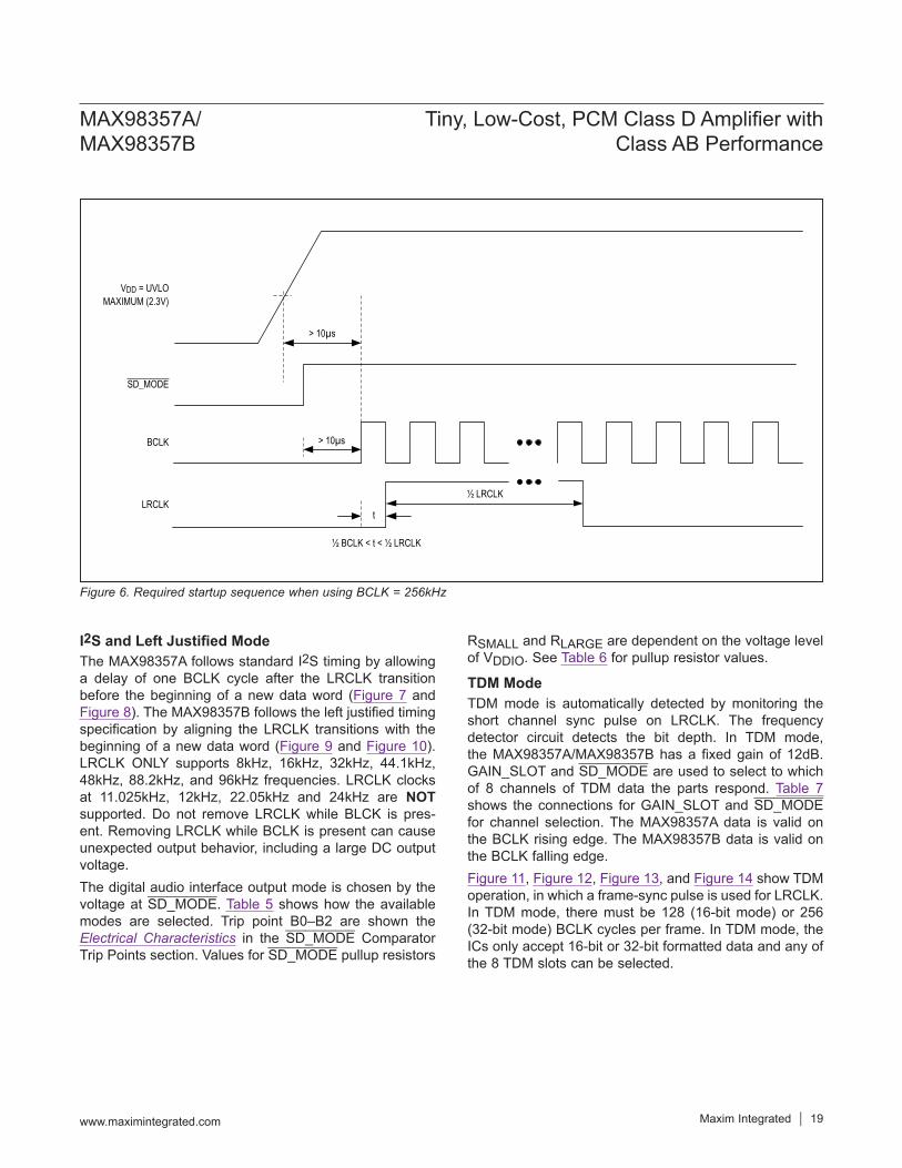
StartupWith the exception of BCLK = 256KHz, the only required sequence for startup is that LRCLK must start within 1/2 LRCLK period of BCLK starting.When using a mode with BCLK = 256kHz, there are addi-tional requirements for the part to power-up properly:1) BCLK and LRCLK cannot be applied before the part
is enabled.2) BCLK and LRCLK must start from logic low and tran-
sition to logic high.3) After VDD is > 2.3V AND SD_MODE is high, there
must be a 10μs wait time before starting BCLK and LRCLK.
4) LRCLK must start at least 1/2 BCLK after BCLK starts.
5) LRCLK must start no more than 1/2 LRCLK after BCLK starts.
6) LRCLK must complete a full cycle; no partial LRCLK cycles.
7) Once started, BCLK and LRCLK must remain switch-ing at 256kHz and 8kHz, respectively, and cannot be interrupted during device operation. If BCLK and LRCLK need to be stopped, SD_MODE must first be set to 0V. Subsequent startups with BCLK = 256kHz and LRCLK = 8kHz need to follow the sequence described in steps 1-6.
Figure 6 shows an example where VDD reaches UVLO maximum before SD_MODE is applied. In this example, the 10μs wait time starts after SD_MODE is applied.
Figure 4. SD_MODE Resistor Connected Using Open-Drain Driver
Figure 5. SD_MODE Resistor Connected Using Push-Pull Driver
GPIO
PROCESSOR VDDIO
R
100kΩ±8%
LEFT MODE
RIGHT MODE
LEFT/2 + RIGHT/2MODE
B2 (1.4V typ)
B1 (0.77V typ)
B0 (0.16V typ)
VSD_MODE
MAX98357AMAX98357B
GPIO
PROCESSOR
VDDIO
R
100kΩ±8%
LEFT MODE
RIGHT MODE
LEFT/2 + RIGHT/2MODE
B2 (1.4V typ)
B1 (0.77V typ)
B0 (0.16V typ)
VSD_MODE
MAX98357AMAX98357B
MAX98357A/MAX98357B
Tiny, Low-Cost, PCM Class D Amplifier with Class AB Performance
www.maximintegrated.com Maxim Integrated 18
I2S and Left Justified ModeThe MAX98357A follows standard I2S timing by allowing a delay of one BCLK cycle after the LRCLK transition before the beginning of a new data word (Figure 7 and Figure 8). The MAX98357B follows the left justified timing specification by aligning the LRCLK transitions with the beginning of a new data word (Figure 9 and Figure 10). LRCLK ONLY supports 8kHz, 16kHz, 32kHz, 44.1kHz, 48kHz, 88.2kHz, and 96kHz frequencies. LRCLK clocks at 11.025kHz, 12kHz, 22.05kHz and 24kHz are NOT supported. Do not remove LRCLK while BLCK is pres-ent. Removing LRCLK while BCLK is present can cause unexpected output behavior, including a large DC output voltage.The digital audio interface output mode is chosen by the voltage at SD_MODE. Table 5 shows how the available modes are selected. Trip point B0–B2 are shown the Electrical Characteristics in the SD_MODE Comparator Trip Points section. Values for SD_MODE pullup resistors
RSMALL and RLARGE are dependent on the voltage level of VDDIO. See Table 6 for pullup resistor values.
TDM ModeTDM mode is automatically detected by monitoring the short channel sync pulse on LRCLK. The frequency detector circuit detects the bit depth. In TDM mode, the MAX98357A/MAX98357B has a fixed gain of 12dB. GAIN_SLOT and SD_MODE are used to select to which of 8 channels of TDM data the parts respond. Table 7 shows the connections for GAIN_SLOT and SD_MODE for channel selection. The MAX98357A data is valid on the BCLK rising edge. The MAX98357B data is valid on the BCLK falling edge.Figure 11, Figure 12, Figure 13, and Figure 14 show TDM operation, in which a frame-sync pulse is used for LRCLK. In TDM mode, there must be 128 (16-bit mode) or 256 (32-bit mode) BCLK cycles per frame. In TDM mode, the ICs only accept 16-bit or 32-bit formatted data and any of the 8 TDM slots can be selected.
Figure 6. Required startup sequence when using BCLK = 256kHz
VDD = UVLO MAXIMUM (2.3V)
BCLK
LRCLK
SD_MODE
½ BCLK < t < ½ LRCLK
½ LRCLK
> 10µs
t
> 10µs
MAX98357A/MAX98357B
Tiny, Low-Cost, PCM Class D Amplifier with Class AB Performance
www.maximintegrated.com Maxim Integrated 19

Figure 7. MAX98357A I2S Digital Audio Interface Timing, 16-Bit Resolution
Table 7. TDM Mode Channel SelectionSD_MODE GAIN_SLOT CHANNEL BITS
Low X Off N/A
VDD GND 0 16/32
VDD VDD with 0Ω 1 16/32
VDD Float 2 16/32
VDD VDD with 100kΩ 3 16/32
VDD GND with 100kΩ 4 16/32
VDD through RLARGE GND 5 16/32
VDD through RLARGE Float 6 16/32
VDD through RLARGE VDD 7 16/32
LRCLK
BCLK
RIGHTLEFT
DIN D15 D14 D13 D12 D11 D10 D9 D8 D7 D6 D5 D4 D3 D2 D1 D0 D15 D14 D13 D12 D11 D10 D9 D8 D7 D6 D5 D4 D3 D2 D1 D0
16 BITS/CHANNEL SD_MODE = VDD
D15 D14
LEFT
LRCLK
BCLK
RIGHTLEFT
IGNORED
DIN D15 D14 D13 D12 D11 D10 D9 D8 D7 D6 D5 D4 D3 D2 D1 D0 D15 D14 D13 D12 D11 D10 D9 D8 D7 D6 D5 D4 D3 D2 D1 D0
16 BITS/CHANNEL SD_MODE PULL UP THROUGH RSMALL (70K)
D15 D14
LEFT
IGNORED
LRCLK
BCLK
RIGHTLEFT
DIN D15 D14 D13 D12 D11 D10 D9 D8 D7 D6 D5 D4 D3 D2 D1 D0 D15 D14 D13 D12 D11 D10 D9 D8 D7 D6 D5 D4 D3 D2 D1 D0
16 BITS/CHANNEL SD_MODE PULL UP THROUGH RLARGE (300k)
D15 D14
LEFT
MAX98357A/MAX98357B
Tiny, Low-Cost, PCM Class D Amplifier with Class AB Performance
www.maximintegrated.com Maxim Integrated 20

Figure 8. MAX98357A I2S Digital Audio Interface Timing, 32-Bit Resolution
D31
D30
D29
D28
D27
D26
D25
D24
D23
D22
D21
D20
D19
D18
D17
D16
D15
D14
D13
D12
D11
D10
D9D8
D7D6
D5D4
D3D2
D1D0
D31
D30
D29
D28
D27
D26
D25
D24
D23
D22
D21
D20
D19
D18
D17
D16
D15
D14
D13
D12
D11
D10
D9D8
D7D6
D5D4
D3D2
D1D0
D31
D30
D31
D30
D29
D28
D27
D26
D25
D24
D23
D22
D21
D20
D19
D18
D17
D16
D15
D14
D13
D12
D11
D10
D9D8
D7D6
D5D4
D3D2
D1D0
D31
D30
D29
D28
D27
D26
D25
D24
D23
D22
D21
D20
D19
D18
D17
D16
D15
D14
D13
D12
D11
D10
D9D8
D7D6
D5D4
D3D2
D1D0
D31
D30
D31
D30
D29
D28
D27
D26
D25
D24
D23
D22
D21
D20
D19
D18
D17
D16
D15
D14
D13
D12
D11
D10
D9D8
D7D6
D5D4
D3D2
D1D0
D31
D30
D29
D28
D27
D26
D25
D24
D23
D22
D21
D20
D19
D18
D17
D16
D15
D14
D13
D12
D11
D10
D9D8
D7D6
D5D4
D3D2
D1D0
D31
D30
LRCL
K
BCLK
RIGH
TLE
FT
DIN
IGNO
RED
LRCL
K
BCLK
RIGH
TLE
FT
DIN
IGNO
RED
LRCL
K
BCLK
RIGH
TLE
FT
DIN
LEFT
AND
RIG
HT S
UMME
D
32 B
ITS/
CHAN
NEL,
SD_M
ODE
= V D
D
32 B
ITS/
CHAN
NEL,
SD_M
ODE
PULL
UP T
HROU
GH R
SMAL
L (70
k)
32 B
ITS/
CHAN
NEL,
SD_M
ODE
PULL
UP T
HROU
GH R
LARG
E (3
00k)
MAX98357A/MAX98357B
Tiny, Low-Cost, PCM Class D Amplifier with Class AB Performance
www.maximintegrated.com Maxim Integrated 21

Figure 9. MAX98357B Left-Justified Digital Audio Interface Timing, 16-Bit Resolution
D14D15 D13 D12 D11 D10 D9 D8 D7 D6 D5 D4 D3 D2 D1 D0 D15 D14 D13 D12 D11 D10 D9 D8 D7 D6 D5 D4 D3 D2 D1 D0 D15 D14
D14D15 D13 D12 D11 D10 D9 D8 D7 D6 D5 D4 D3 D2 D1 D0 D15 D14 D13 D12 D11 D10 D9 D8 D7 D6 D5 D4 D3 D2 D1 D0 D15 D14
D14D15 D13 D12 D11 D10 D9 D8 D7 D6 D5 D4 D3 D2 D1 D0 D15 D14 D13 D12 D11 D10 D9 D8 D7 D6 D5 D4 D3 D2 D1 D0 D15 D14
LRCLK
BCLK
RIGHTLEFT
DIN
16 BITS/CHANNEL, SD_MODE = VDD
IGNORED
IGNORED
LRCLK
BCLK
RIGHTLEFT
DIN
16 BITS/CHANNEL, SD_MODE PULLUP THROUGH RSMALL (70k)
LRCLK
BCLK
RIGHTLEFT
DIN
16 BITS/CHANNEL, SD_MODE PULLUP THROUGH RLARGE (300k)
LEFT AND RIGHT SUMMED
MAX98357A/MAX98357B
Tiny, Low-Cost, PCM Class D Amplifier with Class AB Performance
www.maximintegrated.com Maxim Integrated 22

Figure 10. MAX98357B Left-Justified Digital Audio Interface Timing, 32-Bit Resolution
LRCL
K
BCLK
RIGH
T
LEFT
LEFT
LEFT
DIN
D31
D30
D29
D28
D27
D26
D25
D24
D23
D22
D21
D20
D19
D18
D17
D16
D15
D14
D13
D12
D11
D10
D9D8
D7D6
D5D4
D3D2
D1D0
32 B
ITS/
CHAN
NEL,
SD_M
ODE
= V D
D
D31
D30
32 B
ITS/
CHAN
NEL,
SD_M
ODE
PULL
UP T
HROU
GH R
SMAL
L (70
k)
LEFT
AND
RIG
HT S
UMME
DD29
D28
D27
D26
D25
D24
D23
D22
D21
D20
D19
D18
D17
D16
D15
D14
D13
D12
D11
D10
D9D8
D7D6
D5D4
D3D2
D1
IGNO
RED
D0D3
1D3
0
LEFT
LRCL
K
BCLK
RIGH
T
DIN
32 B
ITS/
CHAN
NEL,
SD_M
ODE
PULL
UP T
HROU
GH R
LARG
E (3
00k)
IGNO
RED
LRCL
K
BCLK
RIGH
T
SDIN
D29
IGNO
RED
LEFT
LEFT
D31
D30
D29
D28
D27
D26
D25
D24
D23
D22
D21
D20
D19
D18
D17
D16
D15
D14
D13
D12
D11
D10
D9D8
D7D6
D5D4
D3D2
D1D0
D31
D30
D29
D28
D27
D26
D25
D24
D23
D22
D21
D20
D19
D18
D17
D16
D15
D14
D13
D12
D11
D10
D9D8
D7D6
D5D4
D3D2
D1D0
D31
D30
D31
D30
D29
D28
D27
D26
D25
D24
D23
D22
D21
D20
D19
D18
D17
D16
D15
D14
D13
D12
D11
D10
D9D8
D7D6
D5D4
D3D2
D1D0
D31
D30
D29
D28
D27
D26
D25
D24
D23
D22
D21
D20
D19
D18
D17
D16
D15
D14
D13
D12
D11
D10
D9D8
D7D6
D5D4
D3D2
D1D0
D31
D30
BCLK
MAX98357A/MAX98357B
Tiny, Low-Cost, PCM Class D Amplifier with Class AB Performance
www.maximintegrated.com Maxim Integrated 23

Figure 11. MAX98357A TDM 16-Bit DAI Timing
D15
D14
D13
D12
D11
D10
D9D8
D7D6
D5D4
D3D2
D1D0
D15
D14
D13
D12
D11
D10
D9D8
D7D6
D5D4
D3D2
D1D0
D15
D14
D13
D12
D11
D10
D9D8
D7D6
D5D4
D3D2
D1D0
IGNO
RED
IGNO
RED
D15
D14
LD3
D0D1
TDM
16-B
IT D
ATA,
128-
BIT
FRAM
E, D
ATA
IN C
HANN
ELS
1-6
IGNO
RED
IGNO
RED
TDM
16-B
IT D
ATA,
128-
BIT
FRAM
E SD
_MOD
E TI
ED T
O V D
D, G
AIN_
SLOT
TIE
D TO
GND
, DAT
A IN
CHA
NNEL
0
TDM
16-B
IT D
ATA,
128-
BIT
FRAM
E SD
_MOD
E TI
ED T
O V D
D TH
ROUG
H RL
ARGE
, GAI
N_SL
OT T
IED
TO V
DD, D
ATA
IN C
HANN
EL 7
MAX98357A/MAX98357B
Tiny, Low-Cost, PCM Class D Amplifier with Class AB Performance
www.maximintegrated.com Maxim Integrated 24
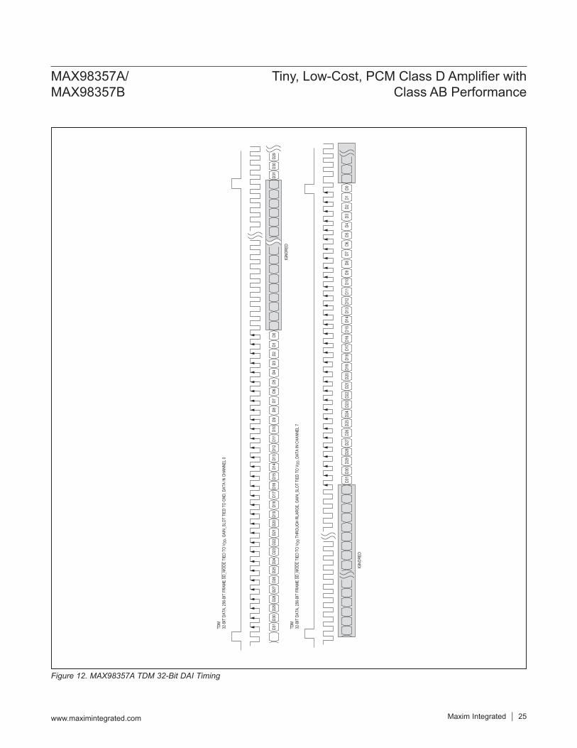
Figure 12. MAX98357A TDM 32-Bit DAI Timing
IGNO
RED
IGNO
RED
TDM
32-B
IT D
ATA,
256-
BIT
FRAM
E SD
_MOD
E TI
ED T
O V D
D TH
ROUG
H RL
ARGE
, GAI
N_SL
OT T
IED
TO V
DD, D
ATA
IN C
HANN
EL 7
TDM
32-B
IT D
ATA,
256-
BIT
FRAM
E SD
_MOD
E TI
ED T
O V D
D, G
AIN_
SLOT
TIE
D TO
GND
, DAT
A IN
CHA
NNEL
0
D31
D31
D30
D29
D30
D29
D28
D27
D26
D25
D24
D23
D22
D21
D20
D19
D18
D17
D16
D15
D14
D13
D12
D11
D10
D9D8
D7D6
D5D4
D3D2
D1D0
D31
D30
D29
D28
D27
D26
D25
D24
D23
D22
D21
D20
D19
D18
D17
D16
D15
D14
D13
D12
D11
D10
D9D8
D7D6
D5D4
D3D2
D1D0
MAX98357A/MAX98357B
Tiny, Low-Cost, PCM Class D Amplifier with Class AB Performance
www.maximintegrated.com Maxim Integrated 25

Figure 13. MAX98357B TDM 16-Bit DAI Timing
TDM
16-B
IT D
ATA,
128-
BIT
FRAM
E SD
_MOD
E TI
ED T
O V D
D, G
AIN_
SLOT
TIE
D TO
GND
, DAT
A IN
CHA
NNEL
0
TDM
16-B
IT D
ATA,
128-
BIT
FRAM
E SD
_MOD
E TI
ED T
O V D
D TH
ROUG
H R L
ARGE
, GAI
N_SL
OT T
IED
TO V
DD, D
ATA
IN C
HANN
EL 7
TDM
16-B
IT D
ATA,
128-
BIT
FRAM
E DA
TA IN
CHA
NNEL
S 1-
6
IGNO
RED
D15
D14
D13
D15
D14
LD3
D12
D11
D10
D9D8
D7D6
D5D4
D3D2
D1D0
IGNO
RED
D15
D15
D14
D13
D12
D11
D10
D9D8
D7D6
D5D4
D3D2
D1D0
D14
D13
D12
D11
D10
D9D8
D7D6
D5D4
D3D2
D1D0
D1D0
IGNO
RED
IGNO
RED
MAX98357A/MAX98357B
Tiny, Low-Cost, PCM Class D Amplifier with Class AB Performance
www.maximintegrated.com Maxim Integrated 26

Figure 14. MAX98357B TDM 32-Bit DAI Timing
TDM
32-B
IT D
ATA,
256-
BIT
FRAM
E SD
_MOD
E TI
ED T
O V D
D, G
AIN_
SLOT
TIE
D TO
GND
, DAT
A IN
CHA
NNEL
0
TDM
32-B
IT D
ATA,
256-
BIT
FRAM
E SD
_MOD
E TI
ED T
O V D
D TH
ROUG
H R L
ARGE
, GAI
N_SL
OT T
IED
TO V
DD, D
ATA
IN C
HANN
EL 7
IGNO
RED
IGNO
RED
D31
D30
D29
D28
D27
D26
D25
D24
D23
D22
D21
D20
D18
D17
D16
D15
D14
D13
D12
D11
D10
D09
D08
D07
D06
D05
D04
D03
D02
D01
D0D3
1D3
0D2
9D1
9
D31
D30
D29
D28
D27
D26
D25
D24
D23
D22
D21
D20
D18
D17
D16
D15
D14
D13
D12
D11
D10
D09
D08
D07
D06
D05
D04
D03
D02
D01
D0D1
9
MAX98357A/MAX98357B
Tiny, Low-Cost, PCM Class D Amplifier with Class AB Performance
www.maximintegrated.com Maxim Integrated 27

Class D Speaker AmplifierThe filterless Class D amplifier offers much higher effi-ciency than Class AB amplifiers. The high efficiency of a Class D amplifier is due to the switching operation of the output stage transistors. Any power loss associated with the Class D output stage is mostly due to the I2R loss of the MOSFET on-resistance and quiescent current overhead.
Ultra-Low EMI Filterless Output StageTraditional Class D amplifiers require the use of external LC filters, or shielding, to meet EN55022B electromagnet-ic-interference (EMI) regulation standards. Maxim’s active emissions-limiting edge-rate control circuitry and spread-spectrum modulation reduces EMI emissions while main-taining up to 92% efficiency.Maxim’s spread-spectrum modulation mode flattens wide-band spectral components while proprietary techniques ensure that the cycle-to-cycle variation of the switching period does not degrade audio reproduction or efficiency. The ICs’ spread-spectrum modulator randomly varies the switching frequency by ±20kHz around the center fre-quency (300kHz). Above 10MHz, the wideband spectrum looks like noise for EMI purposes (Figure 15).
Speaker Current LimitIf the output current of the speaker amplifier exceeds the current limit (2.8A typ), the IC disables the outputs for approximately 100µs. At the end of the 100µs, the outputs are re-enabled. If the fault condition still exists, the IC con-tinues to disable and reenable the outputs until the fault condition is removed.
Gain SelectionThe ICs offer five programmable gain selections through a single gain input (GAIN_SLOT) in I2S/left justified mode. Gain is referenced to the full-scale output of the DAC, which is 2.1dBV (Table 8). In TDM mode, the gain is auto-matically set at a fixed 12dB. Assuming that the desired output swing is not limited by the supply voltage rail, the IC’s output level can be calculated based on the digital input signal level and selected amplifier gain according to the following equation:
Output signal level (dBV) = input signal level (dBFS) + 2.1dB + selected amplifier gain (dB)
where 0dBFS is referenced to 0dBV.
Click-and-Pop SuppressionThe IC speaker amplifier features Maxim’s comprehen-sive click-and-pop suppression. During startup, the click-and-pop suppression circuitry reduces audible transient sources internal to the device by ramping the input signal from mute to 0dB. When entering shutdown, the differen-tial speaker outputs simultaneously drop to GND.The comprehensive click-and-pop suppression of the MAX98357 is unaffected by power-up or power-down sequencing. Applying the DAI clocks before or after the transition of SD_MODE yields the same click-and-pop performance. The MAX98357 does not have a volume ramp-down response when entering shutdown. For opti-mal click-and-pop performance, ramp down the digital data on SDIN before powering down the MAX98357.
Figure 15. EMI with 12in of Speaker Cable and No Output Filtering
Table 8. Gain SelectionGAIN_SLOT I2S/LJ GAIN (dB)
Connect to GND through 100kΩ ±5% resistor 15
Connect to GND 12Unconnected 9
Connect to VDD 6
Connect to VDD through 100kΩ ±5% resistor 3
FREQUENCY (MHz)
EMIS
SION
S LE
VEL (
dBµV
/m)
900800600 700200 300 400 500100
10
30
50
70
90
-100 1000
MAX98357A/MAX98357B
Tiny, Low-Cost, PCM Class D Amplifier with Class AB Performance
www.maximintegrated.com Maxim Integrated 28

Figure 16. Left-Channel PCM Operation with 6dB Gain
Figure 17. Left-Channel PCM Operation with 12dB Gain
Applications Information
OUTP
OUTN
GAIN_SLOT VDD
2.5V TO 5.5V
0.1µF10µF
GPIO*
CODEC
BIT CLOCK
FRAME CLOCK
DATA OUT
SD_MODE
BCLK
LRCLK
DIN
GND
*RESPONDS TO LEFT CHANNEL WHEN GPIO IS HIGH.THE MAX98357A/B ARE SHUT DOWN WHEN GPIO IS LOW.
MAX98357AMAX98357B
B2 A2A1
C1
C3
B1C2
B3
A3
OUTP
OUTN
GAIN_SLOT VDD
2.5V TO 5.5V
0.1µF10µF
GPIO*
CODEC
BIT CLOCK
FRAME CLOCK
DATA OUT
SD_MODE
BCLK
LRCLK
DIN
*RESPONDS TO LEFT CHANNEL WHEN GPIO IS HIGH.THE MAX98357A/B ARE SHUT DOWN WHEN GPIO IS LOW.
MAX98357AMAX98357B
GND
B2 A2A1
C1
C3
B1C2
B3
A3
MAX98357A/MAX98357B
Tiny, Low-Cost, PCM Class D Amplifier with Class AB Performance
www.maximintegrated.com Maxim Integrated 29
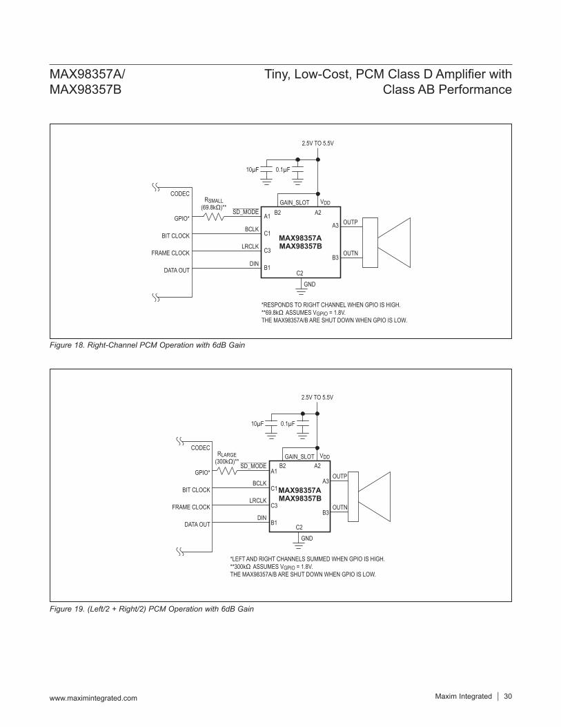
Figure 18. Right-Channel PCM Operation with 6dB Gain
Figure 19. (Left/2 + Right/2) PCM Operation with 6dB Gain
OUTP
OUTN
GAIN_SLOT VDD
2.5V TO 5.5V
0.1µF10µF
SD_MODE
BCLK
LRCLK
RSMALL(69.8kΩ)**
DIN
GND
*RESPONDS TO RIGHT CHANNEL WHEN GPIO IS HIGH.**69.8kΩ ASSUMES VGPIO = 1.8V.THE MAX98357A/B ARE SHUT DOWN WHEN GPIO IS LOW.
MAX98357AMAX98357B
GPIO*
CODEC
BIT CLOCK
FRAME CLOCK
DATA OUT
B2 A2A1
C1
C3
B1C2
B3
A3
OUTP
OUTN
GAIN_SLOT VDD
2.5V TO 5.5V
0.1µF10µF
SD_MODE
BCLK
LRCLK
RLARGE(300kΩ)**
DIN
GND
*LEFT AND RIGHT CHANNELS SUMMED WHEN GPIO IS HIGH.**300kΩ ASSUMES VGPIO = 1.8V.THE MAX98357A/B ARE SHUT DOWN WHEN GPIO IS LOW.
MAX98357AMAX98357B
GPIO*
CODEC
BIT CLOCK
FRAME CLOCK
DATA OUT
B2 A2A1
C1
C3
B1C2
B3
A3
MAX98357A/MAX98357B
Tiny, Low-Cost, PCM Class D Amplifier with Class AB Performance
www.maximintegrated.com Maxim Integrated 30

Figure 20. Stereo PCM Operation Using Two ICs
OUTP
OUTN
GAIN_SLOT VDD
2.5V TO 5.5V
0.1µF10µF
GPIO*
CODEC
BIT CLOCK
FRAME CLOCK
DATA OUT
SD_MODE
BCLK
LRCLK
RSMALL(69.8kΩ)**
DIN
GND
*RESPONDS TO RIGHT CHANNEL WHEN GPIO IS HIGH.**69.8kΩ ASSUMES VGPIO = 1.8V.THE MAX98357A/B ARE SHUT DOWN WHEN GPIO IS LOW.
MAX98357AMAX98357B
OUTP
OUTN
GAIN_SLOT VDD
2.5V TO 5.5V
0.1µF10µF
SD_MODE
BCLK
LRCLK
DIN
GND
*RESPONDS TO CHANNEL 0 WHEN GPIO IS HIGH.THE MAX98357A/B ARE SHUT DOWN WHEN GPIO IS LOW.
MAX98357AMAX98357B
B2 A2A1
C1
C3
B1 C2
B3
A3
B2 A2A1
C1
C3
B1C2
B3
A3
MAX98357A/MAX98357B
Tiny, Low-Cost, PCM Class D Amplifier with Class AB Performance
www.maximintegrated.com Maxim Integrated 31

Figure 21. Channel TDM Operation (Gain Fixed at 12dB)
OUTP
OUTN
GAIN_SLOT VDD
2.5V TO 5.5V
0.1µF 10µF
SD_MODE
BCLK
LRCLK
DIN
GND
*RESPONDS TO CHANNEL 1 WHEN GPIO IS HIGH.THE MAX98357A/B ARE SHUT DOWN WHEN GPIO IS LOW.
*RESPONDS TO CHANNEL 2 WHEN GPIO IS HIGH.THE MAX98357A/B ARE SHUT DOWN WHEN GPIO IS LOW.
MAX98357AMAX98357B
B2 A2A1
C1
C3
B1 C2
B3
A3
OUTP
OUTN
GAIN_SLOT VDD
2.5V TO 5.5V
0.1µF 10µF
SD_MODE
BCLK
LRCLK
DIN
GND
MAX98357AMAX98357B
B2 A2A1
C1
C3
B1 C2
B3
A3
OUTP
OUTN
GAIN_SLOT VDD
2.5V TO 5.5V
0.1µF 10µF
SD_MODE
BCLK
LRCLK
DIN
GND
MAX98357AMAX98357B
B2 A2A1
C1
C3
B1 C2
B3
A3
*RESPONDS TO CHANNEL 3 WHEN GPIO IS HIGH.THE MAX98357A/B ARE SHUT DOWN WHEN GPIO IS LOW.
OUTP
OUTN
GAIN_SLOT VDD
2.5V TO 5.5V
100kΩ0.1µF 10µF
SD_MODE
BCLK
LRCLK
DIN
GND
MAX98357AMAX98357B
B2 A2A1
C1
C3
B1 C2
B3
A3
GPIO*
CODEC
BIT CLOCK
FRAME CLOCK
DATA OUT
*RESPONDS TO CHANNEL 0 WHEN GPIO IS HIGH.THE MAX98357A/B ARE SHUT DOWN WHEN GPIO IS LOW.
MAX98357A/MAX98357B
Tiny, Low-Cost, PCM Class D Amplifier with Class AB Performance
www.maximintegrated.com Maxim Integrated 32

Filterless Class D OperationTraditional Class D amplifiers require an output filter to recover the audio signal from the amplifier’s output. The filter adds cost, size, and decreases efficiency and THD+N performance. The ICs’ filterless modulation scheme does not require an output filter. The device relies on the inherent inductance of the speaker coil and the natural filtering of both the speaker and the human ear to recover the audio component of the square-wave output.Because the switching frequency of the ICs is well beyond the bandwidth of most speakers, voice coil movement due to the switching frequency is very small. Use a speaker with a series inductance > 10µH. Typical 8Ω speakers exhibit series inductances in the 20µH to 100µH range.
Power-Supply InputVDD, which ranges from 2.5V to 5.5V, powers the IC, including the speaker amplifier. Bypass VDD with a 0.1µF and 10µF capacitor to GND. Some applications might require only the 10µF bypass capacitor, making it pos-sible to operate with a single external component. Apply additional bulk capacitance at the ICs if long input traces between VDD and the power source are used.
Layout and GroundingProper layout and grounding are essential for optimum performance. Good grounding improves audio perfor-mance and prevents switching noise from coupling into the audio signal.Use wide, low-resistance output traces. As load imped-ance decreases, the current drawn from the device out-puts increases. At higher current, the resistance of the output traces decreases the power delivered to the load. For example, if 2W is delivered from the speaker output to a 4Ω load through 100mΩ of total speaker trace, 1.904W is being delivered to the speaker. If power is delivered through 10mΩ of total speaker trace, 1.951W is being delivered to the speaker. Wide output, supply, and ground traces also improve the power dissipation of the ICs. Parasitic capacitance on the output traces cause higher quiescent current by VDD x 300kHz x CPARASITIC.For example, at VDD = 5V and a total parasitic capaci-tance of 100pF (50pF on each output trace), the increase in quiescent current is 5 x 300kHz x 100pF = 150µA.The ICs are inherently designed for excellent RF immu-nity. For best performance, add ground fills around all signal traces on top or bottom PCB planes.
Functional Diagram
2.5V TO 5.5V
0.1µF10µF
LRCLK
BCLK
DIN
SD_MODE INTERPOLATOR DAC
CLASS DOUTPUTSTAGE
OUTP
GAIN_SLOTVDD
OUTN
DIGITALAUDIO
INTERFACE
C3
B1
C1
A1
C2
A2 B2
A3
B3
MAX98357AMAX98357B
GND
MAX98357A/MAX98357B
Tiny, Low-Cost, PCM Class D Amplifier with Class AB Performance
www.maximintegrated.com Maxim Integrated 33
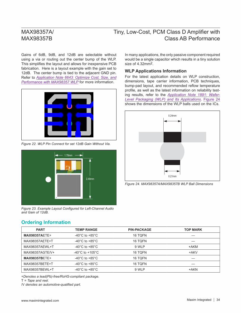
Gains of 6dB, 9dB, and 12dB are selectable without using a via or routing out the center bump of the WLP. This simplifies the layout and allows for inexpensive PCB fabrication. Here is a layout example with the gain set to 12dB. The center bump is tied to the adjacent GND pin. Refer to Application Note 6643: Optimize Cost, Size, and Performance with MAX98357 WLP for more information.
In many applications, the only passive component required would be a single capacitor which results in a tiny solution size of 4.32mm2.
WLP Applications InformationFor the latest application details on WLP construction, dimensions, tape carrier information, PCB techniques, bump-pad layout, and recommended reflow temperature profile, as well as the latest information on reliability test-ing results, refer to the Application Note 1891: Wafer-Level Packaging (WLP) and Its Applications. Figure 24 shows the dimensions of the WLP balls used on the ICs.
Figure 24. MAX98357A/MAX98357B WLP Ball Dimensions
Figure 22. WLP Pin Connect for set 12dB Gain Without Via.
Figure 23. Example Layout Configured for Left-Channel Audio and Gain of 12dB.
+Denotes a lead(Pb)-free/RoHS-compliant package.T = Tape and reel./V denotes an automotive-qualified part.
PART TEMP RANGE PIN-PACKAGE TOP MARKMAX98357AETE+ -40°C to +85°C 16 TQFN —MAX98357AETE+T -40°C to +85°C 16 TQFN —MAX98357AEWL+T -40°C to +85°C 9 WLP +AKMMAX98357AGTE/V+ -40°C to +105°C 16 TQFN +AKVMAX98357BETE+ -40°C to +85°C 16 TQFN —MAX98357BETE+T -40°C to +85°C 16 TQFN —MAX98357BEWL+T -40°C to +85°C 9 WLP +AKN
Ordering Information
1.78mm
2.49mm0.21mm
0.24mm
MAX98357A/MAX98357B
Tiny, Low-Cost, PCM Class D Amplifier with Class AB Performance
www.maximintegrated.com Maxim Integrated 34

PACKAGE TYPE PACKAGE CODE OUTLINE NO. LAND PATTERN NO.9 WLP W91F1+1 21-0896 Refer to Application Note 1891
16 TQFN T1633+4 21-0136 90-0031
Package InformationFor the latest package outline information and land patterns (footprints), go to www.maximintegrated.com/packages. Note that a “+”, “#”, or “-” in the package code indicates RoHS status only. Package drawings may show a different suffix character, but the drawing pertains to the package regardless of RoHS status.
TMintegratedmaxim
0.05 AB
0.05 S
TIE WANG 06/27/14
MAX98357A/MAX98357B
Tiny, Low-Cost, PCM Class D Amplifier with Class AB Performance
www.maximintegrated.com Maxim Integrated 35

Package Information (continued)For the latest package outline information and land patterns (footprints), go to www.maximintegrated.com/packages. Note that a “+”, “#”, or “-” in the package code indicates RoHS status only. Package drawings may show a different suffix character, but the drawing pertains to the package regardless of RoHS status.
MAX98357A/MAX98357B
Tiny, Low-Cost, PCM Class D Amplifier with Class AB Performance
www.maximintegrated.com Maxim Integrated 36

Package Information (continued)For the latest package outline information and land patterns (footprints), go to www.maximintegrated.com/packages. Note that a “+”, “#”, or “-” in the package code indicates RoHS status only. Package drawings may show a different suffix character, but the drawing pertains to the package regardless of RoHS status.
MAX98357A/MAX98357B
Tiny, Low-Cost, PCM Class D Amplifier with Class AB Performance
www.maximintegrated.com Maxim Integrated 37

REVISIONNUMBER
REVISIONDATE DESCRIPTION PAGES
CHANGED0 9/13 Initial release —
1 11/13 Added two new TOCs, replaced TOC 29, updated Figures 1–3, and made variouscorrections
1, 4–20,29–32, 34
2 8/14 Added THD+N for TQFN package with typical spec 53 1/15 Updated spread-spectrum bandwidth spec 5, 284 2/15 Added automotive-qualified part 345 6/15 Updated TOCs 30a and 30b 126 8/15 Corrected package outline for WLP package 367 2/16 Removed future product designations 348 6/16 Removed future product designation on MAX98357AGTE/V+ 34
9 7/17 Updated dynamic range and output noise specifications in Electrical Characteristicstable 5
10 8/17 Updated soldering temperature in the Absolute Maximum Ratings section 4
11 5/18
Updated General Description, Features, and Applications sections, changed Class D Switching Frequency in Electrical Characteristics table and other sections, replaced TOC 20, added DC blocker informaiton to Detailed Description section, updated and added figures to Layout and Grounding section
1, 5, 11, 16, 28, 33, 34
12 4/19Updated Features section to match Electrical Characteristics table typical values.Added Startup section and new Figure 6 for startup requirements when using BCLK = 256kHz
1, 17–34
Revision History
Maxim Integrated cannot assume responsibility for use of any circuitry other than circuitry entirely embodied in a Maxim Integrated product. No circuit patent licenses are implied. Maxim Integrated reserves the right to change the circuitry and specifications without notice at any time. The parametric values (min and max limits) shown in the Electrical Characteristics table are guaranteed. Other parametric values quoted in this data sheet are provided for guidance.
Maxim Integrated and the Maxim Integrated logo are trademarks of Maxim Integrated Products, Inc.
MAX98357A/MAX98357B
Tiny, Low-Cost, PCM Class D Amplifier with Class AB Performance
© 2019 Maxim Integrated Products, Inc. 38
For pricing, delivery, and ordering information, please visit Maxim Integrated’s online storefront at https://www.maximintegrated.com/en/storefront/storefront.html.