Embed Size (px)
Citation preview

General DescriptionThe MAX155/MAX156 are high-speed, 8-bit, multichan-nel analog-to-digital converters (ADCs) with simultaneous track/holds (T/Hs) to eliminate timing differences between input channel samples. The MAX155 has 8 analog input channels and the MAX156 has 4 analog input channels. Each channel has its own T/H, and all T/Hs sample at the same instant. The ADC converts a channel in 3.6µs and stores the result in an internal 8x8 RAM. The MAX155/MAX156 also feature a 2.5V internal reference and power-down capability, providing a complete, sampling data-acquisition system.When operating from a single +5V supply, the MAX155/MAX156 perform either unipolar or bipolar, single-ended or differential conversions. For applications requiring wider dynamic range or bipolar conversions around ground, the VSS supply pin may be connected to -5V.Conversions are initiated with a pulse to the WR pin, and data is accessed from the ADC’s RAM with a pulse to the RD pin. A bidirectional interface updates the channel configuration and provides output data. The ADC may also be wired for output-only operation.The MAX155 comes in 28-pin PDIP and wide SO packages, and the MAX156 comes in 24-pin narrow PDIP and 28-pin wide SO packages.
Features 8 Simultaneously Sampling Track/Hold Inputs 3.6µs Conversion Time Per Channel Unipolar or Bipolar Input Range Single-Ended or Differential Inputs Mixed Input Configurations Possible 2.5V Internal Reference Single +5V or Dual ±5V Supply Operation
Applications Phase-Sensitive Data Acquisition Vibration and Waveform Analysis DSP Analog Input AC Power Meters Portable Data Loggers
Ordering Information appears at end of data sheet.
For related parts and recommended products to use with this part, refer to www.maximintegrated.com/MAX155.related.
AIN0
AIN1T/H
8-BITA/D
3.6µs 2.5VVREF8
8
8
8 x 8RAM
CONTROL LOGIC
THREE-STATE
BUFFER
T/H
AIN2 T/HAIN3 T/HAIN4 T/HAIN5 T/HAIN6 T/HAIN7 T/H
8 8
MODEWRRDCS
CLK
REFIN
REFOUT
8-BITDATA
BUS
MAX155
MAX155/MAX156 8-/4-Channel ADCs with Simultaneous T/Hs and Reference
19-2949; Rev 2; 1/12
Functional Diagram
EVALUATION KIT AVAILABLE

VDD to AGND ............................................................. -0.3V, +6VVDD to DGND ............................................................. -0.3V, +6VAGND to DGND ...........................................-0.3V, (VDD + 0.3V)VSS to AGND.............................................................. +0.3V, -6VVSS to DGND ............................................................. +0.3V, -6V CS, WR, RD, CLK, MODE to DGND ...........-0.3V, (VDD + 0 3V)BUSY, D0–D7 to DGND ...............................-0.3V, (VDD + 0 3V)REFOUT to AGND .......................................-0.3V, (VDD + 0 3V)REFIN to AGND ...........................................-0.3V, (VDD + 0 3V)AIN to AGND .................................... (VSS - 0.3V), (VDD + 0 3V)Output Current (REFOUT) .................................................30mA
Continuous Power Dissipation (TA = +70°C) 24-Pin PDIP (derate 8.7mW/°C above +70°C) ............696mW 28-Pin PDIP (derate 9.09mW/°C above +70°C) ..........727mW 28-Pin Wide SO (derate 12.5mW/°C above +70°C) ..1000mW Operating Temperature Ranges: MAX155/MAX156_C_ _ ......................................0°C to +70°C MAX155/MAX156_E_ _ .................................. -40°C to +85°CStorage Temperature Range ............................ -65°C to +150°CLead Temperature (soldering, 10s) .................................+300°CSoldering Temperature (reflow) .......................................+260°C
(VDD = +5V, VREFIN = +2.5V. External Reference, VAGND = VDGND = 0V, VSS = 0V or -5V, fCLK = 5MHz external, Unipolar range single-ended mode, TA = TMIN to TMAX, unless otherwise noted.)
PARAMETER SYMBOL CONDITIONS MIN TYP MAX UNITSACCURACY (Note 1)Resolution 8 Bits
Integral Linearity ErrorMAX15_A ±½
LSBMAX15_B ±1
No Missing Codes Resolution Guaranteed monotonic 8 Bits
Offset Error (Unipolar)MAX15_A ±½
LSBMAX15_B ±1
Offset Error (Bipolar)MAX15_A ±1
LSBMAX15_B ±2
Gain Error
UnipolarMAX15_A ±1
LSBMAX15_B ±1
BipolarMAX15_A ±1
MAX15_B ±2
Channel-to-Channel MatchingMAX15_A ±½
LSBMAX15_B ±1
DYNAMIC PERFORMANCE (VIN = 50kHz, 2.5VP-P sine wave sampled at 220ksps)
Signal-to-Noise and Distortion Ratio SINAD
MAX15_A 48dB
MAX15_B 47
Total Harmonic Distortion THD -60 dB
Spurious-Free Dynamic Range SFDR -62 dB
Small-Signal Bandwidth 4 MHz
Aperture Delay 20 ns
Aperture Delay Matching (Note 2) 4 ns
MAX155/MAX156 8-/4-Channel ADCs with Simultaneous T/Hs and Reference
www.maximintegrated.com Maxim Integrated 2
Absolute Maximum Ratings
Stresses beyond those listed under “Absolute Maximum Ratings” may cause permanent damage to the device. These are stress ratings only, and functional operation of the device at these or any other conditions beyond those indicated in the operational sections of the specifications is not implied. Exposure to absolute maximum rating conditions for extended periods may affect device reliability.
Electrical Characteristics
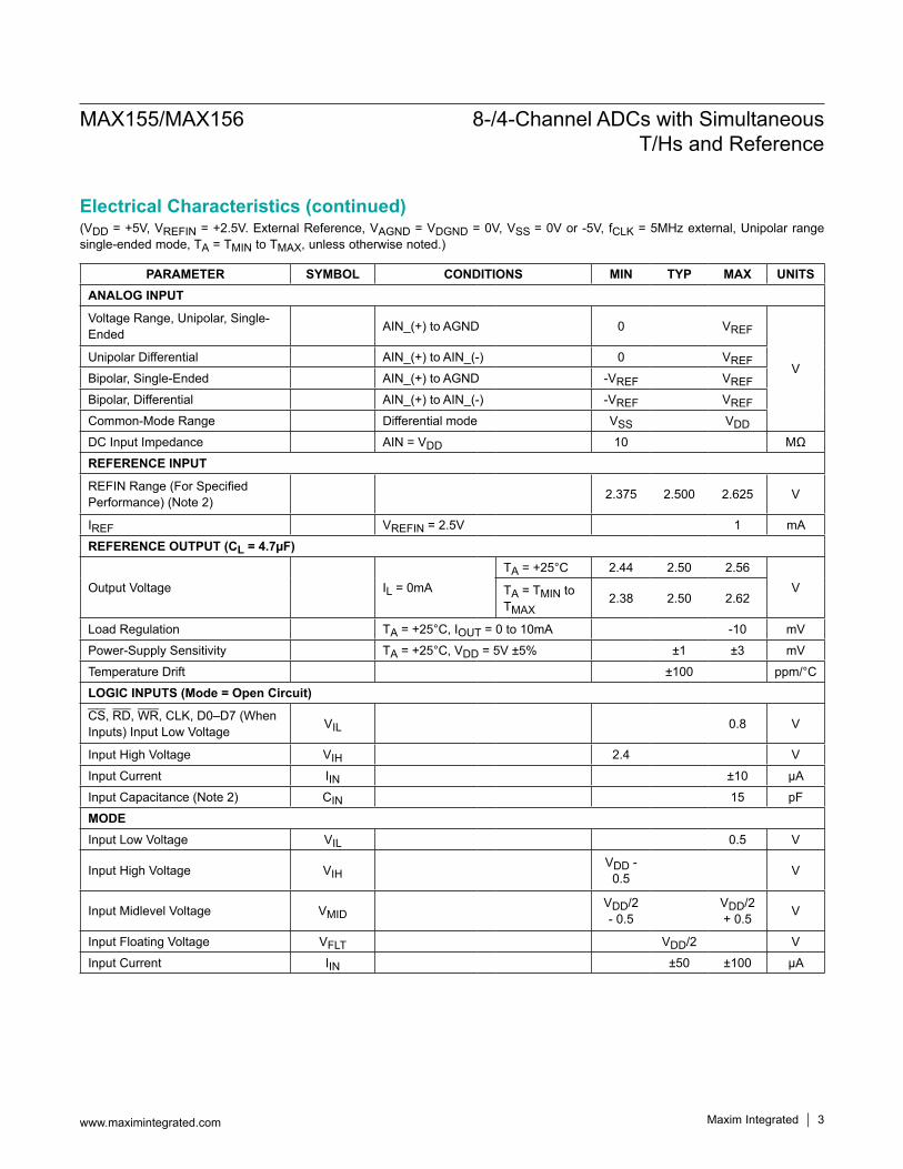
(VDD = +5V, VREFIN = +2.5V. External Reference, VAGND = VDGND = 0V, VSS = 0V or -5V, fCLK = 5MHz external, Unipolar range single-ended mode, TA = TMIN to TMAX, unless otherwise noted.)
PARAMETER SYMBOL CONDITIONS MIN TYP MAX UNITSANALOG INPUT
Voltage Range, Unipolar, Single-Ended AIN_(+) to AGND 0 VREF
VUnipolar Differential AIN_(+) to AIN_(-) 0 VREFBipolar, Single-Ended AIN_(+) to AGND -VREF VREFBipolar, Differential AIN_(+) to AIN_(-) -VREF VREFCommon-Mode Range Differential mode VSS VDDDC Input Impedance AIN = VDD 10 MΩ
REFERENCE INPUT
REFIN Range (For Specified Performance) (Note 2) 2.375 2.500 2.625 V
IREF VREFIN = 2.5V 1 mA
REFERENCE OUTPUT (CL = 4.7µF)
Output Voltage IL = 0mATA = +25°C 2.44 2.50 2.56
VTA = TMIN to TMAX
2.38 2.50 2.62
Load Regulation TA = +25°C, IOUT = 0 to 10mA -10 mV
Power-Supply Sensitivity TA = +25°C, VDD = 5V ±5% ±1 ±3 mV
Temperature Drift ±100 ppm/°C
LOGIC INPUTS (Mode = Open Circuit)
CS, RD, WR, CLK, D0–D7 (When Inputs) Input Low Voltage VIL 0.8 V
Input High Voltage VIH 2.4 V
Input Current IIN ±10 µA
Input Capacitance (Note 2) CIN 15 pF
MODEInput Low Voltage VIL 0.5 V
Input High Voltage VIHVDD -
0.5 V
Input Midlevel Voltage VMIDVDD/2 - 0.5
VDD/2 + 0.5 V
Input Floating Voltage VFLT VDD/2 V
Input Current IIN ±50 ±100 µA
MAX155/MAX156 8-/4-Channel ADCs with Simultaneous T/Hs and Reference
www.maximintegrated.com Maxim Integrated 3
Electrical Characteristics (continued)

(VDD = +5V, VREFIN = +2.5V. External Reference, VAGND = VDGND = 0V, VSS = 0V or -5V, fCLK = 5MHz external, Unipolar range single-ended mode, TA = TMIN to TMAX, unless otherwise noted.)
(VDD = +5V, VREFIN = +2.5V. External Reference, VAGND = VDGND = 0V, VSS = 0V or -5V, TA = TMIN to TMAX, unless otherwise noted.)
PARAMETER SYMBOL CONDITIONS MIN TYP MAX UNITSLOGIC OUTPUTSBUSY, D0–D7 Output Low Voltage VOL IOUT = 1.6mA 0.4 V
Output High Voltage VOH IOUT = -360µA 4 V
D0–D7 Floating State Leakage ±10 µA
Floating State Output Capacitance (Note 2) COUT 15 pF
Conversion Time fCLK = 5MHz, single channel 3.6 3.8 µs
POWER REQUIREMENTSPositive Power-Supply Voltage VDD 4.75 5.25 V
Positive Power-Supply Current IDD
PD = 0MAX155 18 24
mAMAX156 9 12
PD = 1
CLK, CS, WR, RD = 0V or VDD; DOUT = 0V or VDD
25 100 µA
Negative Power-Supply Voltage VSS 0 -5 V
Negative Power-Supply Current ISSPD = 0 2 50
µAPD = 1 2 50
Power-Supply Rejection (Change in Full-Scale Error)
VDD = 5V ±5%, VSS = 0V ±0.1 ±0.25LSB
VDD = 5V, VSS = -5V ±5% ±0.1
PARAMETER SYMBOL CONDITIONS MIN TYP MAX UNITSCS to WR Setup Time tCWS 0 ns
CS to WR Hold Time tCWH 0 ns
CS to RD Setup Time tCRS 0 ns
CS to RD Hold Time (Note 2) tCRH 0 ns
WR Low Pulse Width tWR MAX15_C/E 100 2000 ns
RD Low Pulse Width tRDL MAX15_C/E 100 ns
RD High Pulse Width (Note 2) tRDH MAX15_C/E 180 ns
WR to RD Delay (Note 2) tWRD MAX15_C/E 280 ns
WR to BUSY Low Delay tWBD MAX15_C/E 220 ns
MAX155/MAX156 8-/4-Channel ADCs with Simultaneous T/Hs and Reference
www.maximintegrated.com Maxim Integrated 4
TIMING CHARACTERISTICS (Note 3, Figures 1–7)
Electrical Characteristics (continued)

Note 1: VDD = +5V, VREFIN = +2.5V, VSS = 0V. Performance at ±5% power-supply tolerance is guaranteed by Power-Supply Rejection test.
Note 2: Guaranteed by design, not production tested.Note 3: All input control signals are specified with tr = tf = 20ns (10% to 90% of +5V) and timed from a +1.6V voltage level. Output
signals are timed from VOH and VOL.Note 4: tDV is the time required for an output to cross +0.8V or +2.4V measured with load circuit of Figure 1.Note 5: tTR is the time required for the data lines to change 0.5V, measured with load circuits of Figure 2.
Figure 1. Load Circuits for Data-Access Timing Figure 2. Load Circuits for Three-State Output Timing
PARAMETER SYMBOL CONDITIONS MIN TYP MAX UNITS
BUSY High to WR Delay (to update configuration register) (Notes 2, 3) tBWD 50 ns
CLK to WR Delay (Acquisition Time) (Note 2) tACQ 800 ns
BUSY High to RD Delay (Notes 2, 3) tBRD 50 ns
Address-Setup Time tAS 120 ns
Address-Hold Time tAH 0 ns
RD to Data Valid (Note 4) tDV MAX15_C/E 100 ns
RD to Data Three-State Output (Note 5) tTR MAX15_C/E 80 ns
CLK to BUSY Delay (Note 2) tCB 100 300 ns
CLK Frequency 0.5 5.0 MHz
DN
3kΩ
3kΩ
DGNDHIGH-Z TO VOH
100pFDN
+5V
HIGH-Z TO VOL
100pF
DGND
DN
3kΩ
3kΩ
VOH TO HIGH-Z
10pFDN
+5V
VOL TO HIGH-Z
10pF
MAX155/MAX156 8-/4-Channel ADCs with Simultaneous T/Hs and Reference
www.maximintegrated.com Maxim Integrated 5
TIMING CHARACTERISTICS (Note 3, Figures 1-7) (continued)(VDD = +5V, VREFIN = +2.5V. External Reference, VAGND = VDGND = 0V, VSS = 0V or -5V, TA = TMIN to TMAX, unless otherwise noted.)

Figure 3. Write and Read Timing
tCWS
tWR
tWBD tCONVtBRD
tBWD
tACQ
tRDL tRDH tRDL
tWRD
tCWH tCRS tCRH tCRS tCRH
tCRS
DATA IN DATA OUT DATA OUT
tAHtAS
tDV tDVttR ttR
CS
WR
RD
BUSY
D0–D7
MODE
VSS AGND
1
2
24
23
AIN1
AIN0 AIN3
VDD
AIN2
PDIP
TOP VIEW
3
4
22
21
WR
BUSY D1/A1
5
6
20
19
CS
RD REFOUT
D0/A0
REFIN
7
8
18
17
CLK D29 16
D7/ALL D3/PD10 15
D6/DIFF D4/INH11 14
DGND D5/BIP12 13
MAX156
+
AIN3
N.C.AIN0
1
2
28
27
AIN2
N.C.AIN1
N.C.
N.C
WIDE SO
3
4
26
25
AGND
REFINCS
5 24 VDDMODE
VSS 6
7
23
22
REFOUTRD 8 21
D0/A0WR 9 20
D1/A1BUSY 10 19
D2CLK 11 18
D3/PDD7/ALL 12 17
D4/INHD6/DIFF 13 16
D5/BIPDGND 14 15
+
MAX156
AIN1
AIN0 AIN7
1
2
28
27
AIN3
AIN2 AIN5
AIN6
AIN4
PDIP/SO
3
4
26
25
CS
RD REFOUT
5
6
24
23
MODE
VSS AGND
REFIN
VDD
7
8
22
21
WR D0/A09 20
BUSY D1/A110 19
CLK D2/A211 18
D7/ALL
D6/DIFF
DGND
D3/PD
D4/INH
D5/BIP
12 17
13 16
14 15
+
MAX155
MAX155/MAX156 8-/4-Channel ADCs with Simultaneous T/Hs and Reference
www.maximintegrated.com Maxim Integrated 6
Pin Configuration
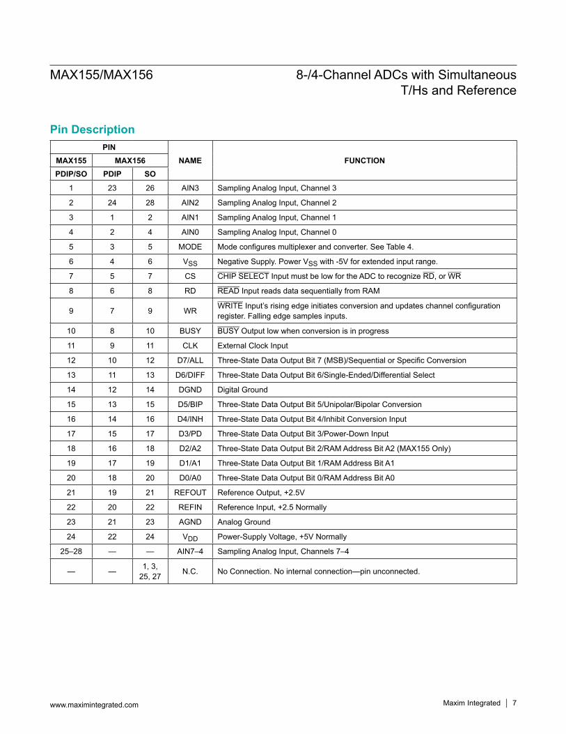
PINNAME FUNCTIONMAX155 MAX156
PDIP/SO PDIP SO
1 23 26 AIN3 Sampling Analog Input, Channel 3
2 24 28 AIN2 Sampling Analog Input, Channel 2
3 1 2 AIN1 Sampling Analog Input, Channel 1
4 2 4 AIN0 Sampling Analog Input, Channel 0
5 3 5 MODE Mode configures multiplexer and converter. See Table 4.
6 4 6 VSS Negative Supply. Power VSS with -5V for extended input range.
7 5 7 CS CHIP SELECT Input must be low for the ADC to recognize RD, or WR
8 6 8 RD READ Input reads data sequentially from RAM
9 7 9 WR WRITE Input’s rising edge initiates conversion and updates channel configuration register. Falling edge samples inputs.
10 8 10 BUSY BUSY Output low when conversion is in progress
11 9 11 CLK External Clock Input
12 10 12 D7/ALL Three-State Data Output Bit 7 (MSB)/Sequential or Specific Conversion
13 11 13 D6/DIFF Three-State Data Output Bit 6/Single-Ended/Differential Select
14 12 14 DGND Digital Ground
15 13 15 D5/BIP Three-State Data Output Bit 5/Unipolar/Bipolar Conversion
16 14 16 D4/INH Three-State Data Output Bit 4/Inhibit Conversion Input
17 15 17 D3/PD Three-State Data Output Bit 3/Power-Down Input
18 16 18 D2/A2 Three-State Data Output Bit 2/RAM Address Bit A2 (MAX155 Only)
19 17 19 D1/A1 Three-State Data Output Bit 1/RAM Address Bit A1
20 18 20 D0/A0 Three-State Data Output Bit 0/RAM Address Bit A0
21 19 21 REFOUT Reference Output, +2.5V
22 20 22 REFIN Reference Input, +2.5 Normally
23 21 23 AGND Analog Ground
24 22 24 VDD Power-Supply Voltage, +5V Normally
25–28 — — AIN7–4 Sampling Analog Input, Channels 7–4
— — 1, 3, 25, 27 N.C. No Connection. No internal connection—pin unconnected.
MAX155/MAX156 8-/4-Channel ADCs with Simultaneous T/Hs and Reference
www.maximintegrated.com Maxim Integrated 7
Pin Description

Detailed DescriptionADC OperationThe MAX155/MAX156 contain a 3.6µs successive approx-imation ADC and 8/4 track-and-hold (T/H) inputs. When a conversion is started, all AIN inputs are simultaneously sampled. All channels sample whether or not they are selected for the conversion. Either a single-channel or multichannel conversion may be requested and channel configurations may be mixed, ADC results are then stored in an internal RAM.In hard-wired mode (see the Multiplexer and AID Configurations section) multichannel conversions are initiated with one write operation. In input/output (I/O) mode, multichannel configurations are set up prior to the conversion by loading channel selections into the con-
figuration register. This register also selects single-ended/differential, unipolar/bipolar (Figure 9), power-down, and other functions. Each channel selection requires a sepa-rate write operation (i.e. 8 writes for 8 channels), but only after power-up. Once the desired channel arrangement is loaded, each subsequent write converts all selected channels without reconfiguring the multiplexer (mux). I/O mode requires more write operations, but provides more flexibility than hard-wired mode.To access conversion results, successive RD pulses auto-matically sence through RAM, beginning with channel 0. Each RD pulse increments the RAM address counter, which resets to 0 when WR goes low in multi channel conversions. An arbitrary RAM location may also be read by writing a 1 to INH while loading the RAM address (A0–A2), and then performing a read operation.
Table 1. Multiplexer Configurations
•Configuration inputs are shared with data outputs D0-D7. The functions of D0-D7 are not described in this table.••DIFF and BIP are not implemented on the current conversion, but go into effect on the.following conversion.
PIN NAME FUNCTION
D0/A0D1/A1D2/A2
1 or 0 A0–A2 select a multiple channel for the configurations described below, or select a RAM address for reading with a subsequent RD.
D3/PD0 Normal ADC operation
1 Power-down reduces the power-supply current. Configuration data may be loaded and is maintained during power-down.
D4/INH0 A conversion starts when WR goes high
1 Inhibits the conversion when WR goes high. Allows mux configuration to be loaded and RAM locations to be accessed without starting a conversion.
D5/BIP**0 Unipolar conversion (Figure 9a) for the channel specified by A0–A2. Input range = 0V to VREF.
1 Bipolar conversion (Figure 9b) for the channel specified by A0–A2. Input range = ±VREF.
D6/DIFF**0 Single-ended configuration for the channel specified by A0–A2 as described in Table 2
1 Differential contiguration for the channel specified by A0–A2 as described in Table 2
D7/ALL0 All previously configured channels are converted. Data is read with consecutive RD pulses,
beginning with the lowest configured channel.
1 Only the channel specified by A2–A0 is converted. A single RD pulse reads the result of that conversion.
MAX155/MAX156 8-/4-Channel ADCs with Simultaneous T/Hs and Reference
www.maximintegrated.com Maxim Integrated 8

Multiplexer and A/D ConfigurationA conversion is started with a WR pulse. All channels sample on WR’s falling edge. Mux configuration data is loaded on WR’s rising edge. In I/O mode (MODE = Open Circuit), selections for channel number, single or multi-channel conversion, unipolar or bipolar input, and single-ended or differential input are made with A0-A2, ALL, BIP, and DIFF (Table 1). These input pins are also shared with the RAM data outputs D0–D7. An alternate, simpler inter-face is provided by the hard-wired mode, which selects some general mux configurations without requiring ADC programming. Hard-wired connections of MODE and VSS
select from 4 mux configurations as listed in Table 4 (see the Hard-Wired Mode section).On the rising edge of WR, the mux configuration register is updated; falling edge initiates sampling of all inputs. A channel selection can be implemented on the current conversion, but changes from unipolar to bipolar (with BIP) or from single ended to differential operation (with DIFF) do not go into effect until the following WR. This can be overcome by writing to the configuration register while inhibiting the conversion (INH = 1), or by changing DIFF and BIP one conversion early, i.e. on the previous write.
Table 2. Single-Ended Channel Selection (MODE = Open Circuit)
Table 3. Differential Channel Selection (MODE = Open Circuit)
Note: Shaded areas represent MAX156 operation.
Note: Shaded areas represent MAX156 operation.
MUX ADDRESS SINGLE-ENDED CHANNEL SELECTIONA0 A1 A2 DIFF 0 1 2 3 4 5 6 7 AGND0 0 0 0 + -
1 0 0 0 + -
0 1 0 0 + -
1 1 0 0 + -
0 0 1 0 + -
1 0 1 0 + -
0 1 1 0 + -
1 1 1 0 + -
MUX ADDRESS DIFFERENTIAL CHANNEL SELECTIONA0 A1 A2 DIFF 0 1 2 3 4 5 6 70 0 0 1 + -
0 1 0 1 + -
0 0 1 1 + -
0 1 1 1 + -
1 0 0 1 - +
1 1 0 1 - +
1 0 1 1 - +
1 1 1 1 - +
MAX155/MAX156 8-/4-Channel ADCs with Simultaneous T/Hs and Reference
www.maximintegrated.com Maxim Integrated 9
Interface TimingInput/Output Mode, Multichannel Conversion Timing I/O mode is selected when the MODE input is open circuit. In I/O mode, the mux configuration register deter-mines the conversion type. The register is updated on the rising edge of WR.Table 1 lists all conversion options. For example, at D6/DIFF, a logic 0 or 1 selects a single-ended or differen-tial conversion. Data is loaded into addressed locations in the configuration register with a series of WR pulses. If INH is high while writing, no conversion takes place. A conversion is started by writing INH = 0 to the configura-tion register. When a change is made to the contents of the configuration register, a “dummy” conversion may be necessary. This is due to a built-in latency of one full con-version for unipolar/bipolar and single-ended/differential selections.It is not necessary to update the configuration register before every conversion. A particular mux configuration must be loaded only once after power-up (but the con-figuration may require several writes to be loaded). A mux configuration is retained for successive conversions and during power-down (PD = 1) so that reconfiguring is unnecessary when the ADC returns to normal operation (PD = 0). Configuration and RAM data is lost only when power is removed from the ADC at VDD.When updating the configuration register, INH should be high for all except the last WR so the conversion is not started until the mux is set. On WR’s falling edge, all input channels sample simultaneously. BUSY goes low at the beginning of the conversion, and channels are converted sequentially starting with the lowest selected channel. When BUSY goes high, conversion results are stored in RAM. At conversion end, a microprocessor (µP) can access the RAM contents with consecutive RD pulses. The first accessed data is the lowest channel’s result.Subsequent RD pulses access conversion results for the remaining channels.
The configuration data determines which RAM locations are sequentially read by consecutive RD pulses, so new data should be placed in the configuration register only after a full RD operation. It is not necessary to update the configuration register for every conversion. A new conver-sion is initiated with a WR pulse (when INH = 0), regard-less of the number of channe ls that have been read.Figure 4a shows the MAX155 timing for an 8-channel unipolar configuration. 8 channels are configured and 8 consecutive RD pulses access data. Figure 4b illus-trates 4-channel differential conversion timing involving 4 sampled channels and 4 RD pulses. In cases where conflicting differential configurations are loaded, the last channel selected with DIFF = 1 will be the positive input of the differential channel.
Input/Output Mode, Single-Channel Conver-sion TimingFigure 5a shows timing for a single-channel (ALL = 1), single-ended conversion; Figure 5b shows a differential conversion. With MODE floating, the configuration reg-ister is updated on the rising edge of WR. BUSY goes low at the beginning of the conversion and returns high when the channel designated by the configuration reg-ister has been converted. All channels are sampled on the falling edge of WR even if only a single channel has been requested. At conversion end, the µP can read the result for the selected channel with a single RD pulse. Subsequent RD pulses will access old conversion results remaining in other RAM locations. The next conversion is initiated with a WR pulse, regardless of the number of channels that have been read.INH and A0–A2, in the configuration register, access loca-tions in RAM. INH = 1 allows the RAM address pointer to be updated without starting a conversion. A READ pulse then reads the contents of the addressed location.
MAX155/MAX156 8-/4-Channel ADCs with Simultaneous T/Hs and Reference
www.maximintegrated.com Maxim Integrated 10

Figure 4a. Input/Output Mode Timing–Eight Single-Ended Conversions
tCONV
CS
WR
RD
BUSY
D0-D7 DATA IN
CONVERSION ENDOF ALL 8 CHANNELS
ACCESSED BY CONSECUTIVE RD PULSESCONSECUTIVE RAM LOCATIONS ARE
UPDATE CONFIGURATIONREGISTER AND BEGIN NEWCONVERSION
ALL 8 CHANNELS ARE SAMPLED HERE
NOTE: After power-up, and prior to the abovetiming sequence, all single-ended channels mustbe set up by writing the following data into theconfiguration register. 8 WRs (see Figure 3) areneeded for 8 channels:
A0 A1 A2 PD INH BIP DIFF ALL0 0 0 0 1 S 0 01 0 0 0 1 S 0 00 1 0 0 1 S 0 01 1 0 0 1 S 0 00 0 1 0 1 S 0 01 0 1 0 1 S 0 00 1 1 0 1 S 0 01 1 1 0 1 S 0 0
CH0 CH1 CH2 CH3
Once the above data is loaded, all channels areconverted with a single WR to any address(this is where the above timing diagram begins).With INH = 0, and ALL = 0:
THE FIRST RAMLOCATION READIS CH 0
S = May be selected
A0 A1 A2 PD INH BIP DIFF ALL0 0 0 0 0 S 0 0
MAX155/MAX156 8-/4-Channel ADCs with Simultaneous T/Hs and Reference
www.maximintegrated.com Maxim Integrated 11

Figure 4b. Input/Output Mode Timing–Four Differential Conversions
tCONV
DATA IN
CONVERSION ENDOF ALL 4 DIFFERENTIAL CHANNELS
ACCESSED BY CONSECUTIVE RD PULSESCONSECUTIVE RAM LOCATIONS ARE
UPDATE CONFIGURATIONREGISTER AND BEGIN NEWCONVERSION
0,1 2,3 4,5 6,7
THE FIRST RAMLOCATION READIS CH 0,1
CS
WR
RD
BUSY
D0-D7
A0 A1 A2 PD INH BIP DIFF ALL0 0 0 0 1 S 0 01 1 0 0 1 S 0 00 0 1 0 1 S 0 01 1 1 0 1 S 0 0
Once the above data is loaded, all channelsare converted with a single WR to any address(this is where the above timing diagram begins).With INH = 0, and ALL = 0:
S = May be selected
A0 A1 A2 PD INH BIP DIFF ALL0 0 0 0 0 S 0 0
NOTE: After power-up, and prior to the abovetiming sequence, all differential channels mustbe set up by writing to the configuration register.(AIN0, 2, 4, 6 are +, and AIN1, 3, 5, 7 are - forthis example). 4 WRs (see Figure 3) are neededfor 8 channels:
ALL 4 DIFFERENTIAL CHANNELSARE SAMPLED HERE
MAX155/MAX156 8-/4-Channel ADCs with Simultaneous T/Hs and Reference
www.maximintegrated.com Maxim Integrated 12
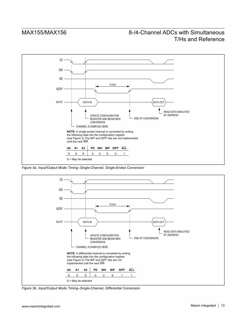
Figure 5a. Input/Output Mode Timing–Single-Channel, Single-Ended Conversion
Figure 5b. Input/Output Mode Timing–Single-Channel, Differential Conversion
tCONV
CS
WR
RD
BUSY
D0-D7 DATA IN DATA OUT
UPDATE CONFIGURATIONREGISTER AND BEGIN NEWCONVERSION
CHANNEL IS SAMPLED HERE
NOTE: A single-ended channel is converted by writingthe following data into the configuration register(see Figure 3) The BIP and DIFF bits are not implementeduntil the next WR
S = May be selected
A0 A1 A2 PD INH BIP DIFF ALL
S S S 0 0 S 0 1
END OF CONVERSION
READ DATA INDICATEDBY ADDRESS
tCONV
CS
WR
RD
BUSY
D0-D7 DATA IN DATA OUT
UPDATE CONFIGURATIONREGISTER AND BEGIN NEWCONVERSION
CHANNEL IS SAMPLED HERE
NOTE: A differential channel is converted by writingthe following data into the configuration register(see Figure 3) The BIP and DIFF bits are notimplemented until the next WR
S = May be selected
A0 A1 A2 PD INH BIP DIFF ALL
S S S 0 0 S 1 1
END OF CONVERSION
READ DATA INDICATEDBY ADDRESS
MAX155/MAX156 8-/4-Channel ADCs with Simultaneous T/Hs and Reference
www.maximintegrated.com Maxim Integrated 13
Hard-Wired ModeFor simpler applications, the MODE and VSS pins can be hard-wired to specify the type of conversion as outlined in Table 4. In this mode, the configuration register is not used, so input data on DO-D7 is ignored. For example, with MODE tied low, an 8-channel, single-ended conver sion begins with WR With MODE tied high, a 4-channel, differential conversion is init iated with WR. Again, the configuration register is not affected by the data present on 00-07. These conversions are otherwise identical to those shown in Figure 4.
Analog Considerationslntemal ReferenceThe internal 2.5V reference (REFOUT) must be bypassed to AGND (Figure 8a) with a 4.7µF electrolytic and a 0.1µF ceramic capacitor to ensure stability.
Figure 6. Input/Output Mode Timing–Reading Arbitrary RAM Locations
Table 4. Hard-Wired Mode—Multiplexer Selections
MODE VSS CONVERSION TYPE
OPEN CIRCUIT X
Multiplexer configuration register determines conversion type. Not hard-wired.
0 AGND 8-Channel, Single-Ended, Unipolar Conversion
1 AGND 4-Channel, Differential, Unipolar Conversion
0 -5V 8-Channel, Single-Ended, Bipolar Conversion
1 -5V 4-Channel, Differential, Bipolar Conversion
INH = 0DATA IN DATA OUT DATA OUTINH = 1
DATA OUTINH = 0DATA IN
UPDATE CONFIGURATION REGISTERAND BEGIN NEW CONVERSION
END OFCONVERSION
READ DATA INDICATEDBY ADDRESS
UPDATE CONFIGURATIONREGISTER WITH NEW ADDRESS
READ DATAAT ADDRESS
UPDATECONFIGURATIONREGISTER BEGIN
CONVERSIONALL CHANNELS ARESAMPLED HERE
NOTE: A RAM location is read by writing the following data into the configuration register and when performing a RD. If INH = 0, a conversion will begin.
S = May be selectedX = Don’t Care for this WR if INH = 0, but may effect next conversion.
A0 A1 A2 PD INH BIP DIFF ALLS S S 0 1 X X 1
tCONV
CS
WR
RD
BUSY
D0-D7
MAX155/MAX156 8-/4-Channel ADCs with Simultaneous T/Hs and Reference
www.maximintegrated.com Maxim Integrated 14
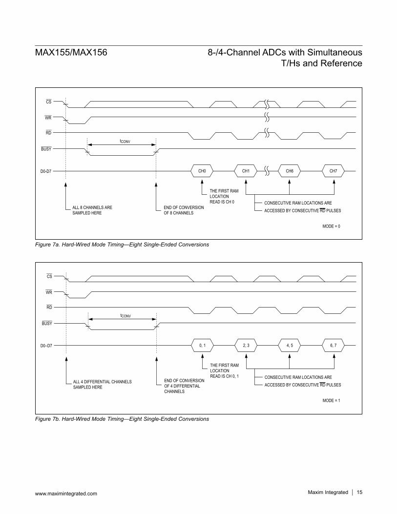
Figure 7a. Hard-Wired Mode Timing—Eight Single-Ended Conversions
Figure 7b. Hard-Wired Mode Timing—Eight Single-Ended Conversions
CH0 CH1 CH6 CH7
tCONV
END OF CONVERSIONOF 8 CHANNELS
THE FIRST RAMLOCATIONREAD IS CH 0 CONSECUTIVE RAM LOCATIONS ARE
ACCESSED BY CONSECUTIVE RD PULSES
MODE = 0
ALL 8 CHANNELS ARESAMPLED HERE
CS
WR
RD
BUSY
D0-D7
0, 1 2, 3 4, 5 6, 7
tCONV
END OF CONVERSIONOF 4 DIFFERENTIALCHANNELS
THE FIRST RAMLOCATIONREAD IS CH 0, 1 CONSECUTIVE RAM LOCATIONS ARE
ACCESSED BY CONSECUTIVE RD PULSES
MODE = 1
ALL 4 DIFFERENTIAL CHANNELSSAMPLED HERE
CS
WR
RD
BUSY
D0–D7
MAX155/MAX156 8-/4-Channel ADCs with Simultaneous T/Hs and Reference
www.maximintegrated.com Maxim Integrated 15

Extemal ReferenceIf an external voltage reference is used at REFIN, REFOUT must either be bypassed (Figure 8b) or dis-abled to prevent its output from oscillating and generating unwanted conversion noise elsewhere in the ADC. If com-ponent count is critical when using an external reference, REFOUT may be disabled by connecting it to VDD. In this case, the unused internal reference does not need a bypass cap. A disadvantage of tying REFOUT to VDD is that power-down current will be increased by about 250µA above the specification limits.
Power-Down ModeThe MAX155/MAX156 may be placed in a powered-down state by writing a 1 to the PD location in the configuration register (Table 1). The register may be updated while in this state (to change mux configurations or exit power-down mode) and all register contents are retained; how-ever no data can be read from RAM and no conversions can be started. The power-down command is implement-ed on WR’s rising edge.To minimize current drain, the MAX155/MAX156 inter-nal reference is turned off during power-down. When returning to normal operation (PD = 0), up to 5ms may be needed to allow the reference to recharge its 4.7µF bypass capacitor before a conversion is performed. If an external reference is used, and remains on during power-down, a conversion can be started within 50µs after load-ing PD with a 0.
BypassingA 47µF electrolytic and a 0.1µF ceramic capacitor should bypass VDD to AGND. If input signals below ground are expected, a negative supply is necessary. In that case, VSS should be bypassed to AGND with a 4.7µF and 0.1µF combination.The internal reference requires a 4.7µF and 0.1µF com-bination. If an external voltage reference is used, bypass REFIN to AGND with a 4.7µF capacitor close to the chip. When an external reference is used, REFOUT must still be either bypassed or connected to VDD.
Track/Hold AmplifiersThe MAX155/MAX156 T/H amplifiers’ high input imped-ance usually requires no input buffering. All T/Hs sample simultaneously. For best results, the analog inputs should not exceed the power-supply rails (VDD, VSS) by more than 50mV.The time required for the T/H to acquire an input signal for one channel is a function of how quickly the channel input capacitance is charged. If the source impedance of the input signal is high, acquisition takes longer, and more time must be allowed between conversions. Acquisition time is calculated by:
tACQ = 8(RS + RIN) x 4pF (but never less than 800ns)where RIN = 15kΩ, and RS = source impedance of the ADC’s input signal.
Figure 8a. Internal Reference Figure 8b. External Reference, +2.5V Full Scale
AINx
REFOUT
REFIN
AGNDVSS
VDD
AINx (+)
AINx (-)
0.1µF4.7µF
0.1µF47µF
+5V
MAX155MAX156
AINx
REFIN
AGNDVSS
REFOUT
VDD
AINx (+)
AINx (-)
0.1µF
+2.5V
4.7µF
0.1µF47µF
+5V
MAX155MAX156
MAX584
4.7µF
MAX155/MAX156 8-/4-Channel ADCs with Simultaneous T/Hs and Reference
www.maximintegrated.com Maxim Integrated 16

Conversion TimeConversion time is calculated by:
tCONV = (9 x N x 2)/fCLKwhere N is the number of channels converted. This includes one clock cycle of uncertainty. For a single channel and 5MHz clock, the conversion time is (9 x 1 x 2)/5MHz = 3.6µs. For the MAX155, the maxi mum conver-sion time for 8 channels is (9 x 8 x 2)/5MHz = 28.8µs. In the application example (Figure 10), six conversions are configured, and the conversion time is (9 x 6 x 2/5MHz = 21.6µs.
Applications Information9-Bit A/D ConversionIn I/O mode, a 9th bit of resolution can be created by per-forming two unipolar differential conversions with opposite input polarities (i.e., first with AIN0[+] and AIN1[-], then with AINO[-] and AIN1[+]). Only the A0 bit must be changed to reverse input channel polarity (Table 3). The sign reversal also occurs on the current write without a one conversion delay. For a differential input signal, one of the two conver-sions will read 0 while the other will contain an 8-bit result. The input polarity that provides the 8-bit result indicates the 9th (sign) bit. 4 channels can be measured this way. A major drawback of this technique is that many of the sam-pling features of the MAX155/MAX156 are defeated since two separate samples are needed If only two 9-bit channels are needed, then two separate differential channels with reversed input polarities can be connected so that both input pairs sample at the same time. This way the simultaneoussampling advantages of the MAX155/MAX156 are retained.
Typical I/O Mode ApplicationThe MAX155/MAX156 address and configuration inputs for this example were determined by selecting the desired channel configurations in Tables 2 and 3. Figure 10 illus-trates the configuration outlined in Table 5.
An A/D conversion in I/O mode involves the following steps:1) Configure the mux by loading data into the con-
figuration register based on selections from Table 2 and/or 3 (with INH = 1 and MODE = open circuit).
Figure 9a. Transfer Function—Unipolar Operation
Figure 9b. Transfer Function—Bipolar Operation
Table 5. Typical Multiplexer ConfigurationA2 A1 A0 DIFF BIP FUNCTION
0 0 1 1 1 Channel (1, 0) Differential Bipolar
0 1 0 0 0 Channel 2 Single-Ended, Unipolar
0 1 1 0 1 Channel 3 Single-Ended, Bipolar
1 0 0 0 1 Channel 4 Single-Ended, Bipolar
1 0 1 0 0 Channel 5 Single-Ended, Unipolar
1 1 0 1 0 Channel (6. 7) Differential, Unipolar
OUTPUTCODE
(FS - 3/2 LSB)
FS = VREFFS256
1 LSB =
1111 11111111 11101111 1101
0000 00110000 00100000 00010000 0000
0 1 LSB2 LSBs
AIN, INPUT VOLTAGE (LSB)
FS - 1 LSB FS
AIN3 LSBs
OUTPUTCODE
FS = 2VREFFS256
1 LSB =
0111 1111
0111 1110
0000 0010
0000 0001
1111 1111
1111 1110
1000 0001
1000 0000
0000 0000+FS - 1 LSB
AIN
-1/2 LSB
+1/2 LSB
MAX155/MAX156 8-/4-Channel ADCs with Simultaneous T/Hs and Reference
www.maximintegrated.com Maxim Integrated 17
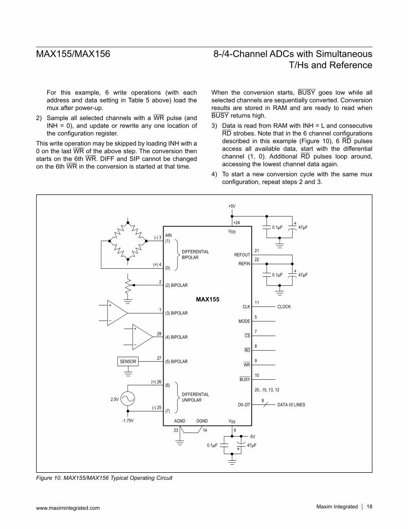
For this example, 6 write operations (with each address and data setting in Table 5 above) load the mux after power-up.
2) Sample all selected channels with a WR pulse (and INH = 0), and update or rewrite any one location of the configuration register.
This write operation may be skipped by loading INH with a 0 on the last WR of the above step. The conversion then starts on the 6th WR. DIFF and SIP cannot be changed on the 6th WR in the conversion is started at that time.
When the conversion starts, BUSY goes low while all selected channels are sequentially converted. Conversion results are stored in RAM and are ready to read when BUSY returns high.3) Data is read from RAM with INH = L and consecutive
RD strobes. Note that in the 6 channel configurations described in this example (Figure 10), 6 RD pulses access all available data, start with the differential channel (1, 0). Additional RD pulses loop around, accessing the lowest chan nel data again.
4) To start a new conversion cycle with the same mux configuration, repeat steps 2 and 3.
Figure 10. MAX155/MAX156 Typical Operating Circuit
MAX155
AIN(1)
DIFFERENTIALBIPOLAR
(0)
(2) BIPOLAR
(-) 3
(+) 4 REFIN
REFOUT22
21
2
(3) BIPOLAR1
DIFFERENTIALUNIPOLAR
(4) BIPOLAR28
(5) BIPOLAR
(6)
(7)
27
2.5V
-1.75V AGND
23 14 6
DGND VSS
(+) 26
(-) 25
SENSOR
47µF
-5V
0.1µF
47µF0.1µFVDD
+5V
+24
47µF0.1µF
CLK CLOCK11
MODE5
CS7
RD8
WR9
BUSY10
20...15, 13, 12
D0–D7 DATA I/0 LINES8
MAX155/MAX156 8-/4-Channel ADCs with Simultaneous T/Hs and Reference
www.maximintegrated.com Maxim Integrated 18

+Denotes a lead(Pb)-free/RoHS-compliant package.*Contact factory for dice specifications.
PART TEMP RANGE PIN-PACKAGE
ERROR (LSBs)
MAX155ACPI+ 0°C to +70°C 28 PDIP ±½
MAX155BCPI+ 0°C to +70°C 28 PDIP ±1
MAX155ACWI+ 0°C to +70°C 28 Wide SO ±½
MAX155BCWI+ 0°C to +70°C 28 Wide SO ±1
MAX155BC/D 0°C to +70°C Dice* ±1
MAX155AEPI+ -40°C to +85°C 28 PDIP ±½
MAX155BEPI+ -40°C to +85°C 28 PDIP ±1
MAX155AEWI+ -40°C to +85°C 28 Wide SO ±½
MAX155BEWI+ -40°C to +85°C 28 Wide SO ±1
MAX156ACNG+ 0°C to +70°C 24 PDIP ±½
MAX156BCNG+ 0°C to +70°C 24 PDIP ±1
MAX156ACWI+ 0°C to +70°C 28 Wide SO ±½
MAX156BCWI+ 0°C to +70°C 28 Wide SO ±1
MAX156BC/D 0°C to +70°C Dice* ±1
MAX156AENG+ -40°C to +85°C 24 PDIP ±½
MAX156BENG+ -40°C to +85°C 24 PDIP ±1
MAX156AEWI+ -40°C to +85°C 28 Wide SO ±½
MAX156BEWI+ -40°C to +85°C 28 Wide SO ±1
PACKAGE TYPE
PACKAGE CODE OUTLINE NO.
LAND PATTERN
NO.24 PDIP N24+8 21-0043 —
28 PDIP P28+7 21-0044 —
28 Wide SO W28+3 21-0042 90-0109
MAX155/MAX156 8-/4-Channel ADCs with Simultaneous T/Hs and Reference
www.maximintegrated.com Maxim Integrated 19
Ordering Information Package InformationFor the latest package outline information and land patterns (footprints), go to www.maximintegrated.com/packages. Note that a “+”, “#”, or “-” in the package code indicates RoHS status only. Package drawings may show a different suffix character, but the drawing pertains to the package regardless of RoHS status.
Chip InformationPROCESS: BiCMOS

REVISIONNUMBER
REVISIONDATE DESCRIPTION PAGES
CHANGED
0 11/91 Initial release —
1 6/94 Revised Figure 9a 16
2 1/12 Removed military grade packages and updated stylistic changes 1–5, 18–20
Maxim Integrated cannot assume responsibility for use of any circuitry other than circuitry entirely embodied in a Maxim Integrated product. No circuit patent licenses are implied. Maxim Integrated reserves the right to change the circuitry and specifications without notice at any time. The parametric values (min and max limits) shown in the Electrical Characteristics table are guaranteed. Other parametric values quoted in this data sheet are provided for guidance.
Maxim Integrated and the Maxim Integrated logo are trademarks of Maxim Integrated Products, Inc.
MAX155/MAX156 8-/4-Channel ADCs with Simultaneous T/Hs and Reference
© 2012 Maxim Integrated Products, Inc. 20
Revision History
For pricing, delivery, and ordering information, please contact Maxim Direct at 1-888-629-4642, or visit Maxim Integrated’s website at www.maximintegrated.com.