Embed Size (px)
Citation preview
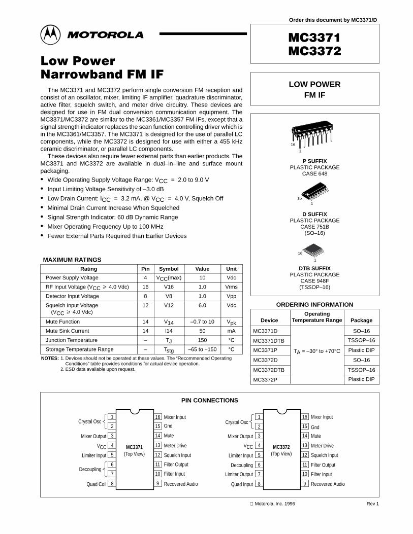
DeviceOperating
Temperature Range Package
LOW POWERFM IF
MC3371D
MC3371DTB
TA = –30° to +70°C
SO–16
TSSOP–16
D SUFFIXPLASTIC PACKAGE
CASE 751B(SO–16)
P SUFFIXPLASTIC PACKAGE
CASE 648
MC3371P
MC3372DTB
Plastic DIP
TSSOP–16
Order this document by MC3371/D
MC3372P Plastic DIP
16
1
161
DTB SUFFIXPLASTIC PACKAGE
CASE 948F(TSSOP–16)
16
1
MC3372D SO–16
ORDERING INFORMATION
1MOTOROLA ANALOG IC DEVICE DATA
The MC3371 and MC3372 perform single conversion FM reception andconsist of an oscillator, mixer, limiting IF amplifier, quadrature discriminator,active filter, squelch switch, and meter drive circuitry. These devices aredesigned for use in FM dual conversion communication equipment. TheMC3371/MC3372 are similar to the MC3361/MC3357 FM IFs, except that asignal strength indicator replaces the scan function controlling driver which isin the MC3361/MC3357. The MC3371 is designed for the use of parallel LCcomponents, while the MC3372 is designed for use with either a 455 kHzceramic discriminator, or parallel LC components.
These devices also require fewer external parts than earlier products. TheMC3371 and MC3372 are available in dual–in–line and surface mountpackaging.
• Wide Operating Supply Voltage Range: VCC = 2.0 to 9.0 V
• Input Limiting Voltage Sensitivity of –3.0 dB
• Low Drain Current: ICC = 3.2 mA, @ VCC = 4.0 V, Squelch Off
• Minimal Drain Current Increase When Squelched
• Signal Strength Indicator: 60 dB Dynamic Range
• Mixer Operating Frequency Up to 100 MHz
• Fewer External Parts Required than Earlier Devices
MAXIMUM RATINGSRating Pin Symbol Value Unit
Power Supply Voltage 4 VCC(max) 10 Vdc
RF Input Voltage (VCC 4.0 Vdc) 16 V16 1.0 Vrms
Detector Input Voltage 8 V8 1.0 Vpp
Squelch Input Voltage(VCC 4.0 Vdc)
12 V12 6.0 Vdc
Mute Function 14 V14 –0.7 to 10 Vpk
Mute Sink Current 14 l14 50 mA
Junction Temperature – TJ 150 °C
Storage Temperature Range – Tstg –65 to +150 °CNOTES: 1. Devices should not be operated at these values. The “Recommended Operating
Conditions” table provides conditions for actual device operation.2. ESD data available upon request.
8
PIN CONNECTIONS
11
Gnd
Mute
Crystal Osc
Meter Drive
Squelch Input
Recovered Audio
Mixer Input
Filter Output
8
Mixer Output
Decoupling
Quad Coil
VCC MC3371(Top View)
3
2
4
5
6
Limiter Input
107
161
15
14
13
12
9
Filter Input
Decoupling
Limiter Output
11
Gnd
Mute
Crystal Osc
Meter Drive
Squelch Input
Recovered Audio
Mixer Input
Filter Output
Mixer Output
Quad Input
VCC MC3372(Top View)
3
2
4
5
6
Limiter Input
107
161
15
14
13
12
9
Filter Input
Motorola, Inc. 1996 Rev 1
MC3371 MC3372
2 MOTOROLA ANALOG IC DEVICE DATA
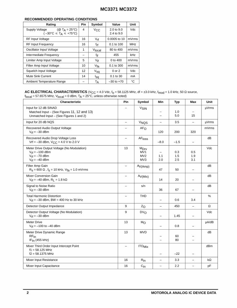
RECOMMENDED OPERATING CONDITIONSRating Pin Symbol Value Unit
Supply Voltage (@ TA = 25°C)( –30°C TA +75°C)
4 VCC 2.0 to 9.02.4 to 9.0
Vdc
RF Input Voltage 16 Vrf 0.0005 to 10 mVrms
RF Input Frequency 16 frf 0.1 to 100 MHz
Oscillator Input Voltage 1 Vlocal 80 to 400 mVrms
Intermediate Frequency – fif 455 kHz
Limiter Amp Input Voltage 5 Vif 0 to 400 mVrms
Filter Amp Input Voltage 10 Vfa 0.1 to 300 mVrms
Squelch Input Voltage 12 Vsq 0 or 2 Vdc
Mute Sink Current 14 lsq 0.1 to 30 mA
Ambient Temperature Range – TA –30 to +70 °C
AC ELECTRICAL CHARACTERISTICS (VCC = 4.0 Vdc, fo = 58.1125 MHz, df = ±3.0 kHz, fmod = 1.0 kHz, 50 Ω source, flocal = 57.6575 MHz, Vlocal = 0 dBm, TA = 25°C, unless otherwise noted)
Characteristic Pin Symbol Min Typ Max Unit
Input for 12 dB SINADMatched Input – (See Figures 11, 12 and 13)Unmatched Input – (See Figures 1 and 2)
– VSIN––
1.05.0
–15
µVrms
Input for 20 dB NQS – VNQS – 3.5 – µVrms
Recovered Audio Output VoltageVrf = –30 dBm
– AFO120 200 320
mVrms
Recovered Audio Drop Voltage LossVrf = –30 dBm, VCC = 4.0 V to 2.0 V
– AFloss–8.0 –1.5 –
dB
Meter Drive Output Voltage (No Modulation)Vrf = –100 dBmVrf = –70 dBmVrf = –40 dBm
13 MDrvMV1MV2MV3
–1.12.0
0.31.52.5
0.51.93.1
Vdc
Filter Amp GainRs = 600 Ω , fs = 10 kHz, Vfa = 1.0 mVrms
– AV(Amp)47 50 –
dB
Mixer Conversion GainVrf = –40 dBm, RL = 1.8 kΩ
– AV(Mix)14 20 –
dB
Signal to Noise RatioVrf = –30 dBm
– s/n36 67 –
dB
Total Harmonic DistortionVrf = –30 dBm, BW = 400 Hz to 30 kHz
– THD– 0.6 3.4
%
Detector Output Impedance 9 ZO – 450 – Ω
Detector Output Voltage (No Modulation)Vrf = –30 dBm
9 DVO– 1.45 –
Vdc
Meter DriveVrf = –100 to –40 dBm
13 MO– 0.8 –
µA/dB
Meter Drive Dynamic RangeRFInIFIn (455 kHz)
13 MVD––
6080
––
dB
Mixer Third Order Input Intercept Pointf1 = 58.125 MHzf2 = 58.1375 MHz
– ITOMix
– –22 –
dBm
Mixer Input Resistance 16 Rin – 3.3 – kΩ
Mixer Input Capacitance 16 Cin – 2.2 – pF
MC3371 MC3372
3MOTOROLA ANALOG IC DEVICE DATA
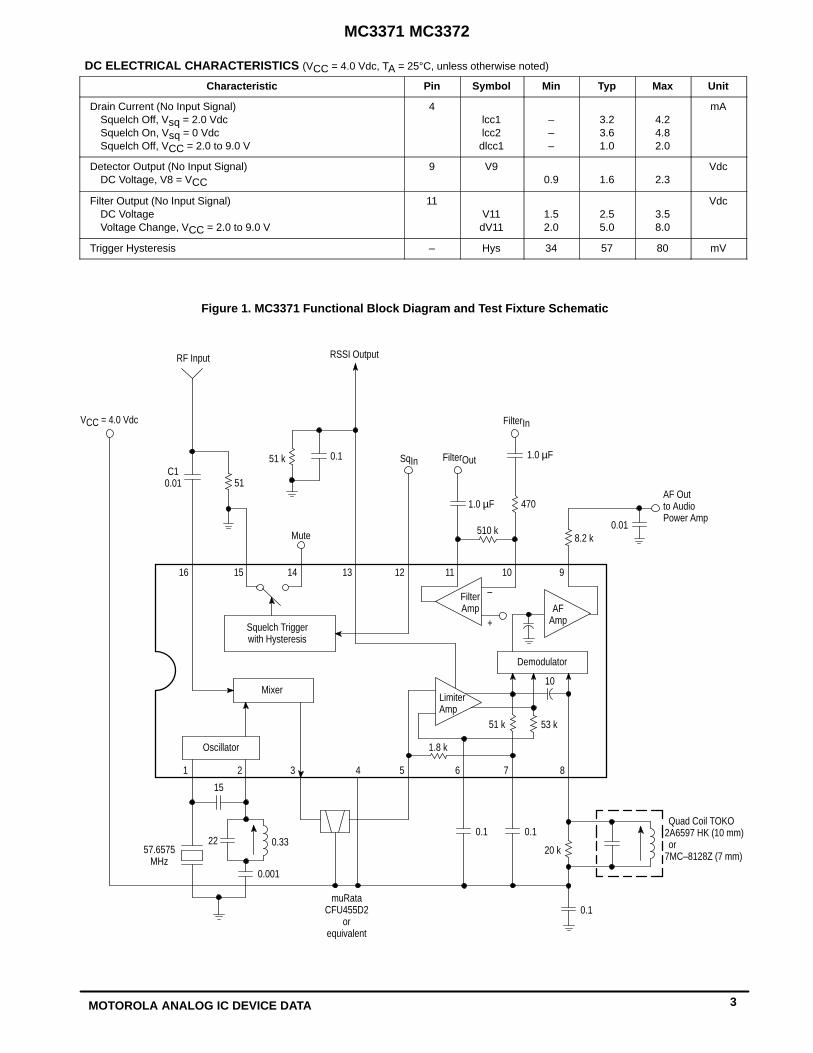
DC ELECTRICAL CHARACTERISTICS (VCC = 4.0 Vdc, TA = 25°C, unless otherwise noted)
Characteristic Pin Symbol Min Typ Max Unit
Drain Current (No Input Signal)Squelch Off, Vsq = 2.0 VdcSquelch On, Vsq = 0 VdcSquelch Off, VCC = 2.0 to 9.0 V
4lcc1lcc2dlcc1
–––
3.23.61.0
4.24.82.0
mA
Detector Output (No Input Signal)DC Voltage, V8 = VCC
9 V90.9 1.6 2.3
Vdc
Filter Output (No Input Signal)DC VoltageVoltage Change, VCC = 2.0 to 9.0 V
11V11dV11
1.52.0
2.55.0
3.58.0
Vdc
Trigger Hysteresis – Hys 34 57 80 mV
Quad Coil TOKO2A6597 HK (10 mm)or
7MC–8128Z (7 mm)
15
22 0.33
0.001
57.6575MHz
Oscillator
0.1 0.1
20 k
0.1muRata
CFU455D2or
equivalent
14
C10.01 51
51 k
RF Input
VCC = 4.0 Vdc
13
2 43 8
–
5 6 71
15
+
16
Mute
0.1
12 11 10 9
FilterOut
1.0 µF
Demodulator
AFAmp
RSSI Output
510 k
SqIn
FilterIn
470
8.2 k0.01
AF Outto AudioPower Amp
53 k
10
LimiterAmp
FilterAmp
Mixer
Squelch Triggerwith Hysteresis
Figure 1. MC3371 Functional Block Diagram and Test Fixture Schematic
1.8 k
51 k
1.0 µF
MC3371 MC3372
4 MOTOROLA ANALOG IC DEVICE DATA
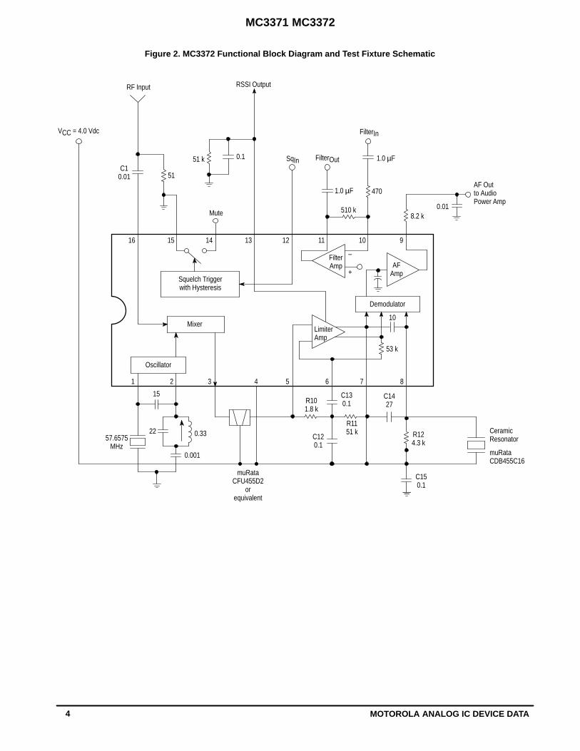
15
22 0.33
0.001
57.6575MHz
Oscillator
C150.1
CeramicResonator
muRataCFU455D2
orequivalent
14
C10.01 51
51 k
RF Input
VCC = 4.0 Vdc
13
2 43 8
–
5 6 71
15
+
16
Mute
0.1
12 11 10 9
FilterOut
1.0 µF
Demodulator
AFAmp
RSSI Output
510 k
SqIn
FilterIn
470
8.2 k0.01
AF Outto AudioPower Amp
53 k
LimiterAmp
FilterAmp
Mixer
Squelch Triggerwith Hysteresis
C1427R10
1.8 k
R1151 k
C120.1
C130.1
R124.3 k
muRataCDB455C16
Figure 2. MC3372 Functional Block Diagram and Test Fixture Schematic
1.0 µF
10
MC3371 MC3372
5MOTOROLA ANALOG IC DEVICE DATA
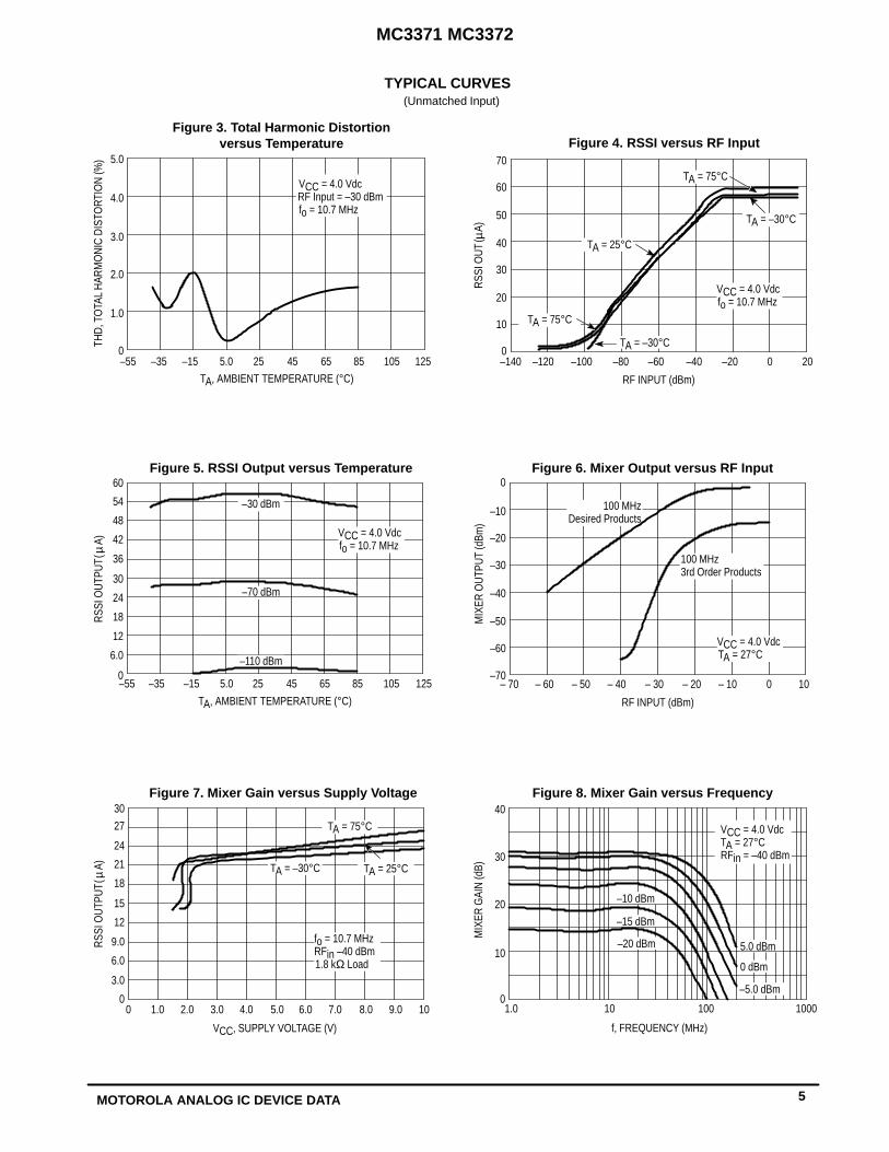
Figure 3. Total Harmonic Distortionversus Temperature
–550
125
20
TA, AMBIENT TEMPERATURE (°C)
5.0 25 45
30
–140
10
40
50
60
–10065 –80 –40–120 –20 0–60 20
TA = –30°C
TA = 25°C
10585
705.0
0
1.0
4.0
3.0
2.0
–35 –15
TA = 75°C
TA = 75°C
TA = –30°C
VCC = 4.0 Vdcfo = 10.7 MHz
RF INPUT (dBm)
THD
, TO
TAL
HAR
MO
NIC
DIS
TORT
ION
(%)
RSS
I OU
T(
A)
µ
Figure 4. RSSI versus RF Input
VCC = 4.0 VdcRF Input = –30 dBmfo = 10.7 MHz
TYPICAL CURVES (Unmatched Input)
RSS
I OU
TPU
T(
A)
µ
–30 dBm
45 6525–35 –15
–70 dBm
TA, AMBIENT TEMPERATURE (°C)
5.0 105–55 12585
VCC = 4.0 Vdcfo = 10.7 MHz
–110 dBm
–20
–10
VCC = 4.0 VdcTA = 27°C
100 MHz3rd Order Products
–50
–60
–40
–30
–70– 20 0 10– 50 – 10– 30– 40– 70
RF INPUT (dBm)
– 60
0
100 MHzDesired Products
MIX
ER O
UTP
UT
(dBm
)
30
18
60
TA = –30°C TA = 25°C
fo = 10.7 MHzRFin –40 dBm1.8 kΩ Load
TA = 75°C
48
54
6.0
42
36
0
24
18
12
6.0
9.0
12
8.0 9.0
21
–5.0 dBm
0 dBm10
–15 dBm
1.0
–20 dBm
–10 dBm
5.0 dBm
40
f, FREQUENCY (MHz)
30
20
010010 1000107.06.05.03.0 4.0
VCC, SUPPLY VOLTAGE (V)
1.0 2.0
30
27
24
0
15
3.0
0
RSS
I OU
TPU
T(
A)
µ
MIX
ER G
AIN
(dB)
Figure 5. RSSI Output versus Temperature Figure 6. Mixer Output versus RF Input
Figure 7. Mixer Gain versus Supply Voltage Figure 8. Mixer Gain versus Frequency
VCC = 4.0 VdcTA = 27°CRFin = –40 dBm
MC3371 MC3372
6 MOTOROLA ANALOG IC DEVICE DATA
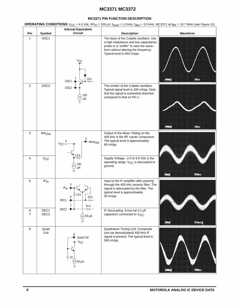
MC3371 PIN FUNCTION DESCRIPTION
OPERATING CONDITIONS VCC = 4.0 Vdc, RFIn = 100 µV, fmod = 1.0 kHz, fdev = 3.0 kHz. MC3371 at fRF = 10.7 MHz (see Figure 11).
Pin SymbolInternal Equivalent
Circuit Description Waveform
1 OSC1
OSC12
VCC
1 15 k
The base of the Colpitts oscillator. Usea high impedance and low capacitanceprobe or a “sniffer” to view the wave–form without altering the frequency. Typical level is 450 mVpp.
2 OSC2
200µA
2OSC2
The emitter of the Colpitts oscillator.Typical signal level is 200 mVpp. Notethat the signal is somewhat distortedcompared to that on Pin 1.
3 MXOut
34 MixerOutVCC
1.5 k
Output of the Mixer. Riding on the 455 kHz is the RF carrier component.The typical level is approximately 60 mVpp.
4 VCC
100µA
1.5 kSupply Voltage –2.0 to 9.0 Vdc is theoperating range. VCC is decoupled toground.
5 IFIn
1.8 k
7 51 kDEC2
53 k
5IFIn
6DEC1
Input to the IF amplifier after passingthrough the 455 kHz ceramic filter. Thesignal is attenuated by the filter. Thetypical level is approximately 50 mVpp.
67
DEC1DEC2
DEC2
60 µA
IF Decoupling. External 0.1 µFcapacitors connected to VCC.
8 QuadCoil
10
VCC
8Quad Coil
50 µA
Quadrature Tuning Coil. Composite(not yet demodulated) 455 kHz IFsignal is present. The typical level is500 mVpp.
MC3371 MC3372
7MOTOROLA ANALOG IC DEVICE DATA
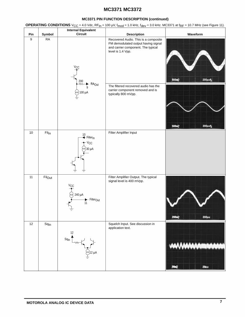
MC3371 PIN FUNCTION DESCRIPTION (continued)
OPERATING CONDITIONS VCC = 4.0 Vdc, RFIn = 100 µV, fmod = 1.0 kHz, fdev = 3.0 kHz. MC3371 at fRF = 10.7 MHz (see Figure 11).
Pin WaveformDescriptionInternal Equivalent
CircuitSymbol
9 RA
RAO t200
VCC
Recovered Audio. This is a compositeFM demodulated output having signaland carrier component. The typicallevel is 1.4 Vpp.
RAOut9
100 µA
The filtered recovered audio has thecarrier component removed and istypically 800 mVpp.
10 FilIn
VCC
10FilterIn
30 µA
Filter Amplifier Input
11 FilOut
11
VCC
FilterOut
240 µA
Filter Amplifier Output. The typicalsignal level is 400 mVpp.
12 SqIn
SqIn
12
12 µA
Squelch Input. See discussion inapplication text.
MC3371 MC3372
8 MOTOROLA ANALOG IC DEVICE DATA
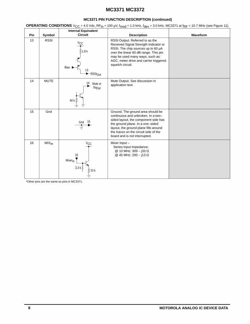
MC3371 PIN FUNCTION DESCRIPTION (continued)
OPERATING CONDITIONS VCC = 4.0 Vdc, RFIn = 100 µV, fmod = 1.0 kHz, fdev = 3.0 kHz. MC3371 at fRF = 10.7 MHz (see Figure 11).
Pin WaveformDescriptionInternal Equivalent
CircuitSymbol
13 RSSI
RSSIOut
1.8 k
Bias13
VCCRSSI Output. Referred to as theReceived Signal Strength Indicator orRSSI. The chip sources up to 60 µAover the linear 60 dB range. This pinmay be used many ways, such as:AGC, meter drive and carrier triggeredsquelch circuit.
14 MUTE
40 k
Mute orSqOut
14Mute Output. See discussion inapplication text.
15 Gnd
Gnd 15
Ground. The ground area should becontinuous and unbroken. In a two–sided layout, the component side hasthe ground plane. In a one–sidedlayout, the ground plane fills aroundthe traces on the circuit side of theboard and is not interrupted.
16 MIXIn
MixerIn
VCC
16
3.3 k10 k
Mixer Input –Series Input Impedance:@ 10 MHz: 309 – j33 Ω@ 45 MHz: 200 – j13 Ω
*Other pins are the same as pins in MC3371.
MC3371 MC3372
9MOTOROLA ANALOG IC DEVICE DATA
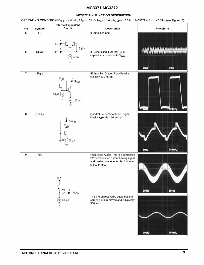
MC3372 PIN FUNCTION DESCRIPTION
OPERATING CONDITIONS VCC = 4.0 Vdc, RFIn = 100 µV, fmod = 1.0 kHz, fdev = 3.0 kHz. MC3372 at fRF = 45 MHz (see Figure 13).
Pin SymbolInternal Equivalent
Circuit Description Waveform
5 IFIn
IFIn5
53 k6
IF Amplifier Input
6 DEC153 k6
DEC
60 µA
IF Decoupling. External 0.1 µFcapacitors connected to VCC.
7 IFOut
IFOut7
120 µA
VCC
50 µA
IF Amplifier Output Signal level istypically 300 mVpp.
8 QuadIn
QuadIn8
50 µA
VCC
10
Quadrature Detector Input. Signal level is typically 150 mVpp.
9 RA
9200RAOut
VCC
Recovered Audio. This is a compositeFM demodulated output having signaland carrier components. Typical levelis 800 mVpp.
RAOut
100 µAThe filtered recovered audio has thecarrier signal removed and is typically500 mVpp.
MC3371 MC3372
10 MOTOROLA ANALOG IC DEVICE DATA
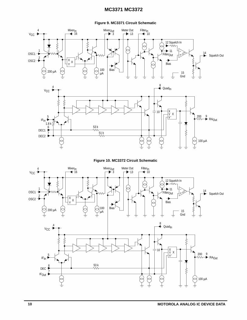
Figure 9. MC3371 Circuit Schematic
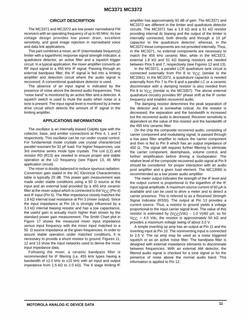
Figure 10. MC3372 Circuit Schematic
100µA
IFOut
8QuadIn
4VCC
5
1.8 kIFIn
DEC153 k
51 k
X
200 9RAOut
100 µA
Squelch Out+FilterOut
Bias
12 Squelch In
11
MixerOut3
Bias
XYX
OSC1
200 µA
2
1
16
14
15Gnd
10FilterIn
–
Meter Out13
OSC2
VCC
4
YY
DEC27
MixerIn
6
X
100µA
Squelch Out+FilterOut
Bias
12 Squelch In
11
MixerOut3
Bias
XY
X
OSC1
200 µA
2
1
16
14
15Gnd
10FilterIn
–
Meter Out13
OSC2
VCC4 MixerIn
8QuadIn
4VCC
5IFIn
DEC53 k
X200 9
RAOut
100 µA
YY
7
6
X
10
10
MC3371 MC3372
11MOTOROLA ANALOG IC DEVICE DATA
CIRCUIT DESCRIPTION
The MC3371 and MC3372 are low power narrowband FMreceivers with an operating frequency of up to 60 MHz. Its lowvoltage design provides low power drain, excellentsensitivity, and good image rejection in narrowband voiceand data link applications.
This part combines a mixer, an IF (intermediate frequency)limiter with a logarithmic response signal strength indicator, aquadrature detector, an active filter and a squelch triggercircuit. In a typical application, the mixer amplifier converts anRF input signal to a 455 kHz IF signal. Passing through anexternal bandpass filter, the IF signal is fed into a limitingamplifier and detection circuit where the audio signal isrecovered. A conventional quadrature detector is used.
The absence of an input signal is indicated by thepresence of noise above the desired audio frequencies. This“noise band” is monitored by an active filter and a detector. Asquelch switch is used to mute the audio when noise or atone is present. The input signal level is monitored by a meterdrive circuit which detects the amount of IF signal in thelimiting amplifier.
APPLICATIONS INFORMATION
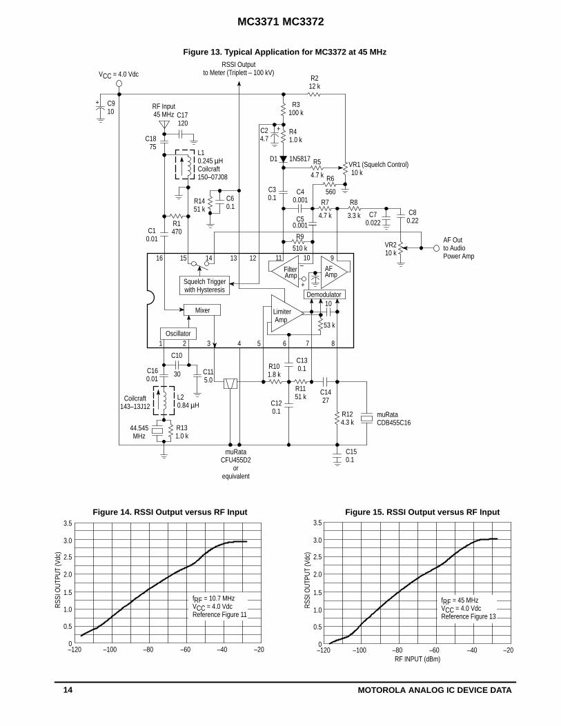
The oscillator is an internally biased Colpitts type with thecollector, base, and emitter connections at Pins 4, 1 and 2respectively. This oscillator can be run under crystal control.For fundamental mode crystals use crystal characterizedparallel resonant for 32 pF load. For higher frequencies, use3rd overtone series mode type crystals. The coil (L2) andresistor RD (R13) are needed to ensure proper and stableoperation at the LO frequency (see Figure 13, 45 MHzapplication circuit).
The mixer is doubly balanced to reduce spurious radiation.Conversion gain stated in the AC Electrical Characteristicstable is typically 20 dB. This power gain measurement wasmade under stable conditions using a 50 Ω source at theinput and an external load provided by a 455 kHz ceramicfilter at the mixer output which is connected to the VCC (Pin 4)and IF input (Pin 5). The filter impedance closely matches the1.8 kΩ internal load resistance at Pin 3 (mixer output). Sincethe input impedance at Pin 16 is strongly influenced by a3.3 kΩ internal biasing resistor and has a low capacitance,the useful gain is actually much higher than shown by thestandard power gain measurement. The Smith Chart plot inFigure 17 shows the measured mixer input impedanceversus input frequency with the mixer input matched to a50 Ω source impedance at the given frequencies. In order toassure stable operation under matched conditions, it isnecessary to provide a shunt resistor to ground. Figures 11,12 and 13 show the input networks used to derive the mixerinput impedance data.
Following the mixer, a ceramic bandpass filter isrecommended for IF filtering (i.e. 455 kHz types having abandwidth of ±2.0 kHz to ±15 kHz with an input and outputimpedance from 1.5 kΩ to 2.0 kΩ). The 6 stage limiting IF
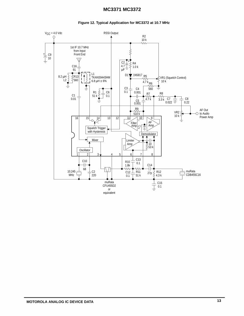
amplifier has approximately 92 dB of gain. The MC3371 andMC3372 are different in the limiter and quadrature detectorcircuits. The MC3371 has a 1.8 kΩ and a 51 kΩ resistorproviding internal dc biasing and the output of the limiter isinternally connected, both directly and through a 10 pFcapacitor to the quadrature detector; whereas, in theMC3372 these components are not provided internally. Thus,in the MC3371, no external components are necessary tomatch the 455 kHz ceramic filter, while in the MC3372,external 1.8 kΩ and 51 kΩ biasing resistors are neededbetween Pins 5 and 7, respectively (see Figures 12 and 13).
In the MC3371, a parallel LCR quadrature tank circuit isconnected externally from Pin 8 to VCC (similar to theMC3361). In the MC3372, a quadrature capacitor is neededexternally from Pin 7 to Pin 8 and a parallel LC or a ceramicdiscriminator with a damping resistor is also needed fromPin 8 to VCC (similar to the MC3357). The above externalquadrature circuitry provides 90° phase shift at the IF centerfrequency and enables recovered audio.
The damping resistor determines the peak separation ofthe detector and is somewhat critical. As the resistor isdecreased, the separation and the bandwidth is increasedbut the recovered audio is decreased. Receiver sensitivity isdependent on the value of this resistor and the bandwidth ofthe 455 kHz ceramic filter.
On the chip the composite recovered audio, consisting ofcarrier component and modulating signal, is passed througha low pass filter amplifier to reduce the carrier componentand then is fed to Pin 9 which has an output impedance of450 Ω . The signal still requires further filtering to eliminatethe carrier component, deemphasis, volume control, andfurther amplification before driving a loudspeaker. Therelative level of the composite recovered audio signal at Pin 9should be considered for proper interaction with an audiopost amplifier and a given load element. The MC13060 isrecommended as a low power audio amplifier.
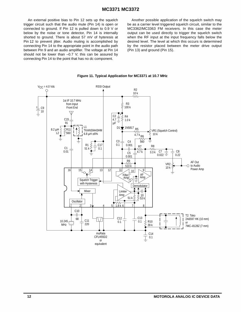
The meter output indicates the strength of the IF level andthe output current is proportional to the logarithm of the IFinput signal amplitude. A maximum source current of 60 µA isavailable and can be used to drive a meter and to detect acarrier presence. This is referred to as a Received StrengthSignal Indicator (RSSI). The output at Pin 13 provides acurrent source. Thus, a resistor to ground yields a voltageproportional to the input carrier signal level. The value of thisresistor is estimated by (VCC(Vdc) – 1.0 V)/60 µA; so forVCC = 4.0 Vdc, the resistor is approximately 50 kΩ andprovides a maximum voltage swing of about 3.0 V.
A simple inverting op amp has an output at Pin 11 and theinverting input at Pin 10. The noninverting input is connectedto 2.5 V. The op amp may be used as a noise triggeredsquelch or as an active noise filter. The bandpass filter isdesigned with external impedance elements to discriminatebetween frequencies. With an external AM detector, thefiltered audio signal is checked for a tone signal or for thepresence of noise above the normal audio band. Thisinformation is applied to Pin 12.
MC3371 MC3372
12 MOTOROLA ANALOG IC DEVICE DATA
An external positive bias to Pin 12 sets up the squelchtrigger circuit such that the audio mute (Pin 14) is open orconnected to ground. If Pin 12 is pulled down to 0.9 V orbelow by the noise or tone detector, Pin 14 is internallyshorted to ground. There is about 57 mV of hyteresis atPin 12 to prevent jitter. Audio muting is accomplished byconnecting Pin 14 to the appropriate point in the audio pathbetween Pin 9 and an audio amplifier. The voltage at Pin 14should not be lower than –0.7 V; this can be assured byconnecting Pin 14 to the point that has no dc component.
Another possible application of the squelch switch maybe as a carrier level triggered squelch circuit, similar to theMC3362/MC3363 FM receivers. In this case the meteroutput can be used directly to trigger the squelch switchwhen the RF input at the input frequency falls below thedesired level. The level at which this occurs is determinedby the resistor placed between the meter drive output(Pin 13) and ground (Pin 15).
Figure 11. Typical Application for MC3371 at 10.7 MHz
–10
C70.022
VR1 (Squelch Control)10 k
VR210 k
AF Outto AudioPower Amp
3.3 k
R8
C10
6810.245MHz
L1TKANS9443HM6.8 µH ±6%
D1
+
1N5817 R5
R64.7 k
560
R7
R9
4.7 k
510 k
1053 k51 k
+
8.2 µHL2
1st IF 10.7 MHzfrom InputFront End+
T2: Toko2A6597 HK (10 mm)or7MC–8128Z (7 mm)
VCC = 4.0 Vdc RSSI OutputR2
10 k
C80.22
R11560
C910
R151 kC1
0.01
C170.1
C30.1
C40.001
C50.001
C11220
C130.1 R10
39 k
C140.1
14 131516 12 11 9
2 43 85 6 71Oscillator
muRataCFU455D2
orequivalent
Demodulator
Filter
Mixer
Squelch Triggerwith Hysteresis
AF
LimiterAmp
1.8 k
C120.1
C24.7µF
C1591
R3100 k
R41.0 k
AmpAmp
MC3371 MC3372
13MOTOROLA ANALOG IC DEVICE DATA
Figure 12. Typical Application for MC3372 at 10.7 MHz
–10
C70.022
VR1 (Squelch Control)10 k
VR210 k
AF Outto AudioPower Amp
3.3 k
R8
C10
6810.245MHz
L1TKANS9443HM6.8 µH ± 6%
D1
+
1N5817 R5
R64.7 k
560
R7
R9
4.7 k
510 k
53 k
+
8.2 µHL2
1st IF 10.7 MHzfrom InputFront End+
VCC = 4.0 Vdc RSSI OutputR2
10 k
C80.22
R13560
C910
R151 kC1
0.01
C60.1
C30.1
C40.001
C5
C2220
C14
14 131516 12 11 9
2 43 85 6 71Oscillator
muRataCFU455D2
orequivalent
Demodulator
Filter
Mixer
Squelch Triggerwith Hysteresis
AF
Limiter Amp
C150.1
R101.8k
R1151 k
C120.1
C130.1
R124.3 k
27p muRataCDB455C16
C1691
C24.7µF
R41.0 k
AmpAmp
0.001
10
MC3371 MC3372
14 MOTOROLA ANALOG IC DEVICE DATA
2.0
2.5
–20–40–60–80
3.5
3.0
1.5
1.0
0.5
0–120 –100
RSS
I OU
TPU
T (V
dc)
fRF = 10.7 MHzVCC = 4.0 VdcReference Figure 11
Figure 13. Typical Application for MC3372 at 45 MHz
Figure 14. RSSI Output versus RF Input Figure 15. RSSI Output versus RF Input
–
RSSI Outputto Meter (Triplett – 100 kV)
3.5
3.0
muRataCDB455C16
RF INPUT (dBm)
1.5
1.0
0.5
0–120 –100 –80 –60 –40
2.5
–20
2.0
C70.022
VR1 (Squelch Control)10 k
VR210 k
AF Outto AudioPower Amp
3.3 k
R8
L10.245 µHCoilcraft150–07J08
D1
+
1N5817
R64.7 k
560R7
R9
4.7 k
510 k
RF Input45 MHz
+
VCC = 4.0 Vdc R212 k
C80.22
C1875
C910
R1451 k
C10.01
C60.1
C30.1
C40.001
C5
C24.7
R3100 k
R41.0 k
R5
R1470
53 k
14 131516 12 11 10 9
2 43 85 6 71Oscillator
Demodulator
Filter
Mixer
Squelch Triggerwith Hysteresis
AF
Limiter Amp
C10
30C160.01
C115.0
R101.8 k
R1151 k
R124.3 k
C150.1
muRataCFU455D2
orequivalent
C130.1
C1427C12
0.1
R131.0 k
44.545MHz
Coilcraft143–13J12
L20.84 µH
C17120
RSS
I OU
TPU
T (V
dc)
+
0.001
AmpAmp
fRF = 45 MHzVCC = 4.0 VdcReference Figure 13
10
MC3371 MC3372
15MOTOROLA ANALOG IC DEVICE DATA
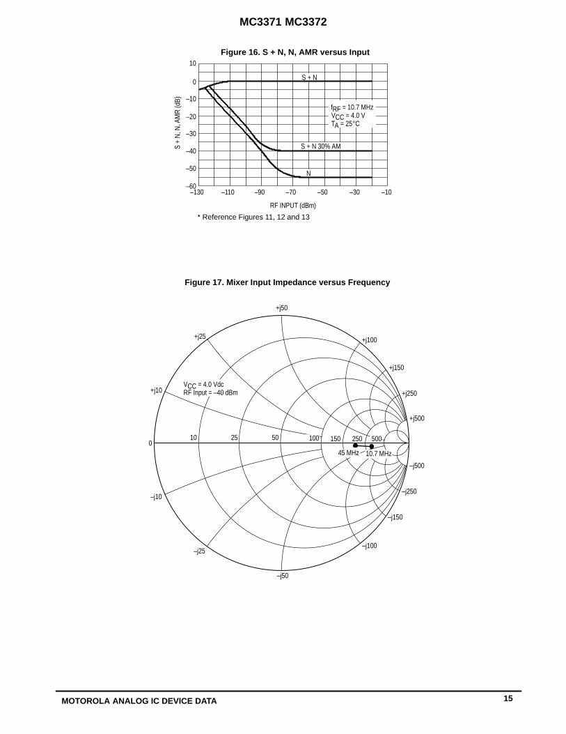
Figure 16. S + N, N, AMR versus Input
Figure 17. Mixer Input Impedance versus Frequency
+j10
–j500
–j250
–j150
–j100
–j50
–j25
–j10
+j250
+j25
+j50
+j500
+j150
VCC = 4.0 VdcRF Input = –40 dBm
+j100
010 150 50025025 50
N
–60–70 –10–30–50–90–110
10
0
–10
–130
–50
–40
–30
–20
* Reference Figures 11, 12 and 13
RF INPUT (dBm)
S + N
S + N 30% AM
10.7 MHz45 MHz
S +
N, N
, AM
R (d
B)
100
fRF = 10.7 MHzVCC = 4.0 VTA = 25°C
MC3371 MC3372
16 MOTOROLA ANALOG IC DEVICE DATA
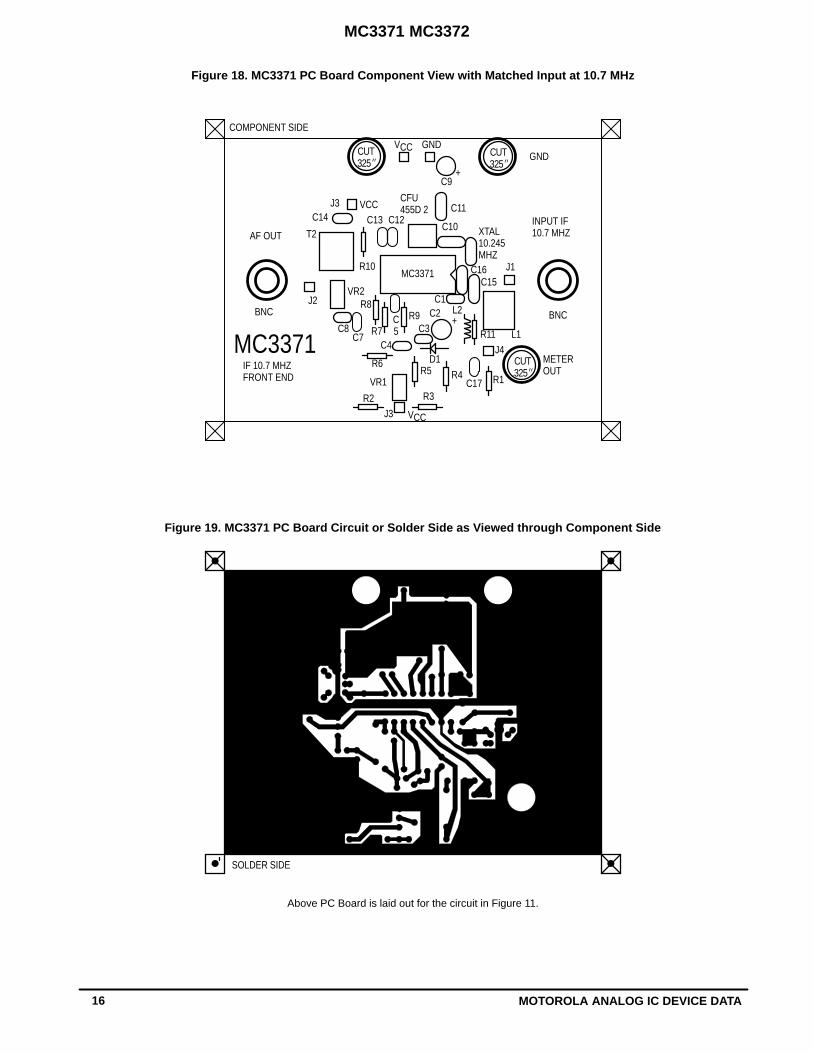
Figure 18. MC3371 PC Board Component View with Matched Input at 10.7 MHz
Figure 19. MC3371 PC Board Circuit or Solder Side as Viewed through Component Side
METEROUT
J4
R1
C3R9
D1
C5
R5 R4C17
R3
R6
VR1
VCCJ3
VR2R8
R7C8C7
C1L2C2+
C15
INPUT IF10.7 MHZ
J1
L1MC3371IF 10.7 MHZFRONT END
C14
BNC
J3
XTAL10.245MHZ
C10
C11CFU455D 2VCC
C13
MC3371R10
J2
T2AF OUT
BNC
GNDCUT.325
+C9
VCC
COMPONENT SIDE
R11
C16
C12
GND
R2
C4
Above PC Board is laid out for the circuit in Figure 11.
SOLDER SIDE
CUT.325
CUT.325
MC3371 MC3372
17MOTOROLA ANALOG IC DEVICE DATA
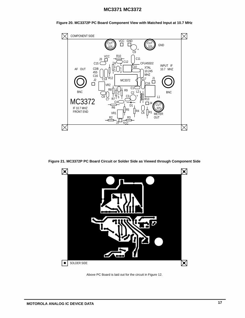
Figure 20. MC3372P PC Board Component View with Matched Input at 10.7 MHz
Figure 21. MC3372P PC Board Circuit or Solder Side as Viewed through Component Side
CDB455C16
CFU455D2INPUT IF10.7 MHZ
C15J3
C10
C11VCC
AF OUT
GNDCUT.325
+C9
VCC
COMPONENT SIDE
C12
GNDCUT.325
R10
R11
C13
METEROUT
J4
R1
C3
R9
D1R5 R4 C6
R3
R6
VR1
VCCJ3
VR2
R8
R7C8
C7
C1C2
+
C16
J1
L1
MC3372IF 10.7 MHZFRONT END
BNC
XTAL10.245MHZ
MC3372R12
J2
BNC
R13
C17
R2
C4CUT.325
C5
L2
C14
Above PC Board is laid out for the circuit in Figure 12.
SOLDER SIDE
MC3371 MC3372
18 MOTOROLA ANALOG IC DEVICE DATA
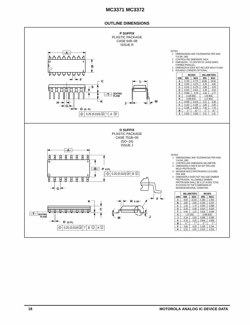
OUTLINE DIMENSIONS
D SUFFIXPLASTIC PACKAGE
CASE 751B–05(SO–16)ISSUE J
P SUFFIXPLASTIC PACKAGE
CASE 648–08ISSUE R
NOTES:1. DIMENSIONING AND TOLERANCING PER ANSI
Y14.5M, 1982.2. CONTROLLING DIMENSION: INCH.3. DIMENSION L TO CENTER OF LEADS WHEN
FORMED PARALLEL.4. DIMENSION B DOES NOT INCLUDE MOLD FLASH.5. ROUNDED CORNERS OPTIONAL.
–A–
B
F C
S
HG
D
J
L
M
16 PL
SEATING
1 8
916
K
PLANE–T–
MAM0.25 (0.010) T
DIM MIN MAX MIN MAXMILLIMETERSINCHES
A 0.740 0.770 18.80 19.55B 0.250 0.270 6.35 6.85C 0.145 0.175 3.69 4.44D 0.015 0.021 0.39 0.53F 0.040 0.70 1.02 1.77G 0.100 BSC 2.54 BSCH 0.050 BSC 1.27 BSCJ 0.008 0.015 0.21 0.38K 0.110 0.130 2.80 3.30L 0.295 0.305 7.50 7.74M 0 10 0 10 S 0.020 0.040 0.51 1.01
NOTES:1. DIMENSIONING AND TOLERANCING PER ANSI
Y14.5M, 1982.2. CONTROLLING DIMENSION: MILLIMETER.3. DIMENSIONS A AND B DO NOT INCLUDE
MOLD PROTRUSION.4. MAXIMUM MOLD PROTRUSION 0.15 (0.006)
PER SIDE.5. DIMENSION D DOES NOT INCLUDE DAMBAR
PROTRUSION. ALLOWABLE DAMBARPROTRUSION SHALL BE 0.127 (0.005) TOTALIN EXCESS OF THE D DIMENSION ATMAXIMUM MATERIAL CONDITION.
1 8
16 9
SEATINGPLANE
F
JM
R X 45
G
8 PLP–B–
–A–
M0.25 (0.010) B S
–T–
D
K
C
16 PL
SBM0.25 (0.010) A ST
DIM MIN MAX MIN MAXINCHESMILLIMETERS
A 9.80 10.00 0.386 0.393B 3.80 4.00 0.150 0.157C 1.35 1.75 0.054 0.068D 0.35 0.49 0.014 0.019F 0.40 1.25 0.016 0.049G 1.27 BSC 0.050 BSCJ 0.19 0.25 0.008 0.009K 0.10 0.25 0.004 0.009M 0 7 0 7 P 5.80 6.20 0.229 0.244R 0.25 0.50 0.010 0.019
MC3371 MC3372
19MOTOROLA ANALOG IC DEVICE DATA
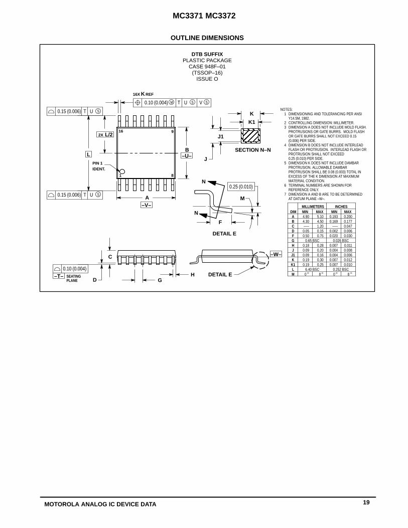
OUTLINE DIMENSIONS
DTB SUFFIXPLASTIC PACKAGE
CASE 948F–01(TSSOP–16)
ISSUE O
ÇÇÇÇÇÇÇÇÇ
DIM MIN MAX MIN MAXINCHESMILLIMETERS
A 4.90 5.10 0.193 0.200B 4.30 4.50 0.169 0.177C ––– 1.20 ––– 0.047D 0.05 0.15 0.002 0.006F 0.50 0.75 0.020 0.030G 0.65 BSC 0.026 BSCH 0.18 0.28 0.007 0.011J 0.09 0.20 0.004 0.008J1 0.09 0.16 0.004 0.006K 0.19 0.30 0.007 0.012K1 0.19 0.25 0.007 0.010L 6.40 BSC 0.252 BSCM 0 8 0 8
NOTES:1 DIMENSIONING AND TOLERANCING PER ANSI
Y14.5M, 1982.2 CONTROLLING DIMENSION: MILLIMETER.3 DIMENSION A DOES NOT INCLUDE MOLD FLASH.
PROTRUSIONS OR GATE BURRS. MOLD FLASHOR GATE BURRS SHALL NOT EXCEED 0.15(0.006) PER SIDE.
4 DIMENSION B DOES NOT INCLUDE INTERLEADFLASH OR PROTRUSION. INTERLEAD FLASH ORPROTRUSION SHALL NOT EXCEED0.25 (0.010) PER SIDE.
5 DIMENSION K DOES NOT INCLUDE DAMBARPROTRUSION. ALLOWABLE DAMBARPROTRUSION SHALL BE 0.08 (0.003) TOTAL INEXCESS OF THE K DIMENSION AT MAXIMUMMATERIAL CONDITION.
6 TERMINAL NUMBERS ARE SHOWN FORREFERENCE ONLY.
7 DIMENSION A AND B ARE TO BE DETERMINEDAT DATUM PLANE –W–.
SECTION N–N
SEATINGPLANE
IDENT.PIN 1
1 8
16 9
DETAIL E
J
J1
B
C
D
A
K
K1
HG
ÉÉÉÉÉÉ
DETAIL E
F
M
L
2X L/2
–U–
SU0.15 (0.006) T
SU0.15 (0.006) T
SUM0.10 (0.004) V ST
0.10 (0.004)–T–
–V–
–W–
0.25 (0.010)
16X REFK
N
N

MC3371 MC3372
20 MOTOROLA ANALOG IC DEVICE DATA
Motorola reserves the right to make changes without further notice to any products herein. Motorola makes no warranty, representation or guarantee regardingthe suitability of its products for any particular purpose, nor does Motorola assume any liability arising out of the application or use of any product or circuit, andspecifically disclaims any and all liability, including without limitation consequential or incidental damages. “Typical” parameters which may be provided in Motoroladata sheets and/or specifications can and do vary in different applications and actual performance may vary over time. All operating parameters, including “Typicals”must be validated for each customer application by customer’s technical experts. Motorola does not convey any license under its patent rights nor the rights ofothers. Motorola products are not designed, intended, or authorized for use as components in systems intended for surgical implant into the body, or otherapplications intended to support or sustain life, or for any other application in which the failure of the Motorola product could create a situation where personal injuryor death may occur. Should Buyer purchase or use Motorola products for any such unintended or unauthorized application, Buyer shall indemnify and hold Motorolaand its officers, employees, subsidiaries, affiliates, and distributors harmless against all claims, costs, damages, and expenses, and reasonable attorney feesarising out of, directly or indirectly, any claim of personal injury or death associated with such unintended or unauthorized use, even if such claim alleges thatMotorola was negligent regarding the design or manufacture of the part. Motorola and are registered trademarks of Motorola, Inc. Motorola, Inc. is an EqualOpportunity/Affirmative Action Employer.
Mfax is a trademark of Motorola, Inc.How to reach us:USA/EUROPE/Locations Not Listed : Motorola Literature Distribution; JAPAN : Nippon Motorola Ltd.: SPD, Strategic Planning Office, 4–32–1,P.O. Box 5405, Denver, Colorado 80217. 303–675–2140 or 1–800–441–2447 Nishi–Gotanda, Shinagawa–ku, Tokyo 141, Japan. 81–3–5487–8488
Mfax : [email protected] – TOUCHTONE 602–244–6609 ASIA/PACIFIC : Motorola Semiconductors H.K. Ltd.; 8B Tai Ping Industrial Park,– US & Canada ONLY 1–800–774–1848 51 Ting Kok Road, Tai Po, N.T., Hong Kong. 852–26629298
INTERNET: http://motorola.com/sps
MC3371/D◊