Embed Size (px)
Citation preview
HC05MC68HC05B6/D
Rev. 3
MC68HC05B4MC68HC705B5MC68HC05B6MC68HC05B8MC68HC05B16MC68HC705B16MC68HC05B32MC68HC705B32
TECHNICALDATA
MC
68HC
05B6
!MO
TO
RO
LAT
EC
HN
ICA
L DA
TA

1
2
3
4
5
6
7
8
9
10
11
12
13
14
15
INTRODUCTION
MODES OF OPERATION AND PIN DESCRIPTIONS
MEMORY AND REGISTERS
INPUT/OUTPUT PORTS
PROGRAMMABLE TIMER
SERIAL COMMUNICATIONS INTERFACE
PULSE LENGTH D/A CONVERTERS
ANALOG TO DIGITAL CONVERTER
RESETS AND INTERRUPTS
CPU CORE AND INSTRUCTION SET
ELECTRICAL SPECIFICATIONS
MECHANICAL DATA
ORDERING INFORMATION
APPENDICES
HIGH SPEED OPERATION
1
2
3
4
5
6
7
8
9
10
11
12
13
14
15
INTRODUCTION
MODES OF OPERATION AND PIN DESCRIPTIONS
MEMORY AND REGISTERS
INPUT/OUTPUT PORTS
PROGRAMMABLE TIMER
SERIAL COMMUNICATIONS INTERFACE
PULSE LENGTH D/A CONVERTERS
ANALOG TO DIGITAL CONVERTER
RESETS AND INTERRUPTS
CPU CORE AND INSTRUCTION SET
ELECTRICAL SPECIFICATIONS
MECHANICAL DATA
ORDERING INFORMATION
MC68HC05B4
HIGH SPEED OPERATION
2
1
3
4
5
6
7
8
9
10
11
12
13
14
15
All products are sold on Motorola’s Terms & Conditions of Supply. In ordering a product covered by this document theCustomer agrees to be bound by those Terms & Conditions and nothing contained in this document constitutes or forms partof a contract (with the exception of the contents of this Notice). A copy of Motorola’s Terms & Conditions of Supply is availableon request.
Motorola reserves the right to make changes without further notice to any products herein. Motorola makes no warranty,representation or guarantee regarding the suitability of its products for any particular purpose, nor does Motorola assume anyliability arising out of the application or use of any product or circuit, and specifically disclaims any and all liability, includingwithout limitation consequential or incidental damages. “Typical” parameters can and do vary in different applications. Alloperating parameters, including “Typicals”, must be validated for each customer application by customer’s technical experts.Motorola does not convey any license under its patent rights nor the rights of others. Motorola products are not designed,intended, or authorized for use as components in systems intended for surgical implant into the body, or other applicationsintended to support or sustain life, or for any other application in which the failure of the Motorola product could create asituation where personal injury or death may occur. Should Buyer purchase or use Motorola products for any such unintendedor unauthorized application, Buyer shall indemnify and hold Motorola and its officers, employees, subsidiaries, affiliates, anddistributors harmless against all claims, costs, damages, and expenses, and reasonable attorney fees arising out of, directlyor indirectly, any claim of personal injury or death associated with such unintended or unauthorized use, even if such claimalleges that Motorola was negligent regarding the design or manufacture of the part. Motorola and !are registered trademarksof Motorola, Inc. Motorola, Inc. is an Equal Opportunity/Affirmative Action Employer.
The Customer should ensure that it has the most up to date version of the document by contacting its local Motorola office.This document supersedes any earlier documentation relating to the products referred to herein. The information containedin this document is current at the date of publication. It may subsequently be updated, revised or withdrawn.
© MOTOROLA LTD., 1995
All Trade Marks recognised. This document contains information on new products. Specifications and information herein aresubject to change without notice.
MC68HC05B6
High-density ComplementaryMetal Oxide Semiconductor
(HCMOS) Microcomputer Unit

2
1
3
4
5
6
7
8
9
10
11
12
13
14
15
CAUTIONThis document includes descriptions of the variousself-check and bootstrap mechanisms that arecurrently implemented as firmware in the non-userROM areas of the MC68HC05B6 and related devices.
As these firmware routines are intended primarily tohelp Motorola’s engineers test the devices, they maybe changed or removed at any time.
For this reason, Motorola recommends that theself-check and bootstrap routines are not called fromfrom the user software. Customers who do call theseroutines from the user software do so at their own risk.
MC68HC05B6 MOTOROLAi
TABLE OF CONTENTS
ParagraphNumber
PageNumberTitle
1INTRODUCTION
1.1 Features................................................................................................................ 1-21.2 Mask options for the MC68HC05B6 ..................................................................... 1-2
2MODES OF OPERATION AND PIN DESCRIPTIONS
2.1 Modes of operation ............................................................................................... 2-12.1.1 Single chip mode ............................................................................................ 2-12.1.2 Self-check mode ............................................................................................. 2-12.2 Serial RAM loader ................................................................................................ 2-42.3 ‘Jump to any address’ ........................................................................................... 2-42.4 Low power modes................................................................................................. 2-72.4.1 STOP .............................................................................................................. 2-72.4.2 WAIT ............................................................................................................... 2-92.4.2.1 Power consumption during WAIT mode .................................................... 2-92.4.3 SLOW mode.................................................................................................... 2-102.4.3.1 Miscellaneous register ............................................................................. 2-102.5 Pin descriptions ................................................................................................... 2-112.5.1 VDD and VSS ................................................................................................. 2-112.5.2 IRQ ................................................................................................................. 2-112.5.3 RESET ............................................................................................................ 2-112.5.4 TCAP1 ............................................................................................................ 2-112.5.5 TCAP2 ............................................................................................................ 2-122.5.6 TCMP1............................................................................................................ 2-122.5.7 TCMP2............................................................................................................ 2-122.5.8 OSC1, OSC2 .................................................................................................. 2-122.5.8.1 Crystal ....................................................................................................... 2-122.5.8.2 Ceramic resonator..................................................................................... 2-122.5.8.3 External clock ............................................................................................ 2-132.5.9 RDI (Receive data in)...................................................................................... 2-142.5.10 TDO (Transmit data out).................................................................................. 2-142.5.11 SCLK............................................................................................................... 2-14
MOTOROLAii
MC68HC05B6
Table of Contents (continued)
ParagraphNumber
PageNumberTitle
2.5.12 PLMA ...............................................................................................................2-142.5.13 PLMB ...............................................................................................................2-142.5.14 VPP1................................................................................................................2-142.5.15 VRH .................................................................................................................2-142.5.16 VRL..................................................................................................................2-142.5.17 PA0 – PA7/PB0 – PB7/PC0 – PC7...................................................................2-142.5.18 PD0/AN0–PD7/AN7.........................................................................................2-14
3MEMORY AND REGISTERS
3.1 Registers ...............................................................................................................3-13.2 RAM.......................................................................................................................3-13.3 ROM ......................................................................................................................3-13.4 Self-check ROM ....................................................................................................3-23.5 EEPROM...............................................................................................................3-33.5.1 EEPROM control register ................................................................................3-33.5.2 EEPROM read operation .................................................................................3-53.5.3 EEPROM erase operation ...............................................................................3-53.5.4 EEPROM programming operation ...................................................................3-63.5.5 Options register (OPTR) ..................................................................................3-63.6 EEPROM during STOP mode ...............................................................................3-73.7 EEPROM during WAIT mode ................................................................................3-73.8 Miscellaneous register .........................................................................................3-9
4INPUT/OUTPUT PORTS
4.1 Input/output programming .....................................................................................4-14.2 Ports A and B ........................................................................................................4-24.3 Port C ....................................................................................................................4-34.4 Port D ....................................................................................................................4-34.5 Port registers .........................................................................................................4-44.5.1 Port data registers A and B (PORTA and PORTB) ..........................................4-44.5.2 Port data register C (PORTC)..........................................................................4-44.5.3 Port data register D (PORTD)..........................................................................4-54.5.3.1 A/D status/control register..........................................................................4-54.5.4 Data direction registers (DDRA, DDRB and DDRC)........................................4-54.6 Other port considerations ......................................................................................4-6
MC68HC05B6 MOTOROLAiii
Table of Contents (continued)
ParagraphNumber
PageNumberTitle
5PROGRAMMABLE TIMER
5.1 Counter ................................................................................................................. 5-15.1.1 Counter register and alternate counter register ............................................ 5-35.2 Timer control and status ....................................................................................... 5-45.2.1 Timer control register (TCR) ........................................................................... 5-45.2.2 Timer status register (TSR)............................................................................. 5-65.3 Input capture......................................................................................................... 5-75.3.1 Input capture register 1 (ICR1) ....................................................................... 5-75.3.2 Input capture register 2 (ICR2) ....................................................................... 5-85.4 Output compare .................................................................................................... 5-95.4.1 Output compare register 1 (OCR1)................................................................. 5-95.4.2 Output compare register 2 (OCR2)................................................................. 5-105.4.3 Software force compare .................................................................................. 5-115.5 Pulse Length Modulation (PLM) ........................................................................... 5-115.5.1 Pulse length modulation registers A and B (PLMA/PLMB) .......................... 5-115.6 Timer during STOP mode..................................................................................... 5-125.7 Timer during WAIT mode...................................................................................... 5-125.8 Timer state diagrams ............................................................................................ 5-12
6SERIAL COMMUNICATIONS INTERFACE
6.1 SCI two-wire system features ............................................................................... 6-16.2 SCI receiver features ............................................................................................ 6-36.3 SCI transmitter features........................................................................................ 6-36.4 Functional description........................................................................................... 6-36.5 Data format ........................................................................................................... 6-56.6 Receiver wake-up operation ................................................................................. 6-56.6.1 Idle line wake-up ............................................................................................. 6-66.6.2 Address mark wake-up ................................................................................... 6-66.7 Receive data in (RDI) ........................................................................................... 6-66.8 Start bit detection.................................................................................................. 6-66.9 Transmit data out (TDO) ....................................................................................... 6-86.10 SCI synchronous transmission ............................................................................. 6-96.11 SCI registers ......................................................................................................... 6-106.11.1 Serial communications data register (SCDR) ............................................... 6-106.11.2 Serial communications control register 1 (SCCR1) ...................................... 6-106.11.3 Serial communications control register 2 (SCCR2) ........................................ 6-146.11.4 Serial communications status register (SCSR) ............................................. 6-16
MOTOROLAiv
MC68HC05B6
Table of Contents (continued)
ParagraphNumber
PageNumberTitle
6.11.5 Baud rate register (BAUD) ...............................................................................6-186.12 Baud rate selection................................................................................................6-196.13 SCI during STOP mode.........................................................................................6-216.14 SCI during WAIT mode..........................................................................................6-21
7PULSE LENGTH D/A CONVERTERS
7.1 Miscellaneous register ..........................................................................................7-37.2 PLM clock selection...............................................................................................7-47.3 PLM during STOP mode .......................................................................................7-47.4 PLM during WAIT mode ........................................................................................7-4
8ANALOG TO DIGITAL CONVERTER
8.1 A/D converter operation.........................................................................................8-18.2 A/D registers..........................................................................................................8-38.2.1 Port D data register (PORTD)..........................................................................8-38.2.2 A/D result data register (ADDATA) ...................................................................8-38.2.3 A/D status/control register (ADSTAT)...............................................................8-48.3 A/D converter during STOP mode.........................................................................8-58.4 A/D converter during WAIT mode..........................................................................8-68.5 Port D analog input................................................................................................8-6
9RESETS AND INTERRUPTS
9.1 Resets ...................................................................................................................9-19.1.1 Power-on reset.................................................................................................9-29.1.2 Miscellaneous register ...................................................................................9-29.1.3 RESET pin .......................................................................................................9-39.1.4 Computer operating properly (COP) watchdog reset.......................................9-39.1.4.1 COP watchdog during STOP mode ...........................................................9-49.1.4.2 COP watchdog during WAIT mode ............................................................9-49.1.5 Functions affected by reset..............................................................................9-59.2 Interrupts ...............................................................................................................9-69.2.1 Interrupt priorities.............................................................................................9-69.2.2 Nonmaskable software interrupt (SWI) ............................................................9-69.2.3 Maskable hardware interrupts..........................................................................9-7
MC68HC05B6 MOTOROLAv
Table of Contents (continued)
ParagraphNumber
PageNumberTitle
9.2.3.1 External interrupt (IRQ) ............................................................................. 9-79.2.3.2 Miscellaneous register ............................................................................. 9-99.2.3.3 Timer interrupts ......................................................................................... 9-109.2.3.4 Serial communications interface (SCI) interrupts ...................................... 9-109.2.4 Hardware controlled interrupt sequence ......................................................... 9-11
10CPU CORE AND INSTRUCTION SET
10.1 Registers............................................................................................................. 10-110.1.1 Accumulator (A) ............................................................................................ 10-210.1.2 Index register (X)........................................................................................... 10-210.1.3 Program counter (PC) ................................................................................... 10-210.1.4 Stack pointer (SP) ......................................................................................... 10-210.1.5 Condition code register (CCR)...................................................................... 10-210.2 Instruction set ..................................................................................................... 10-310.2.1 Register/memory Instructions ....................................................................... 10-410.2.2 Branch instructions ....................................................................................... 10-410.2.3 Bit manipulation instructions ......................................................................... 10-410.2.4 Read/modify/write instructions ...................................................................... 10-410.2.5 Control instructions ....................................................................................... 10-410.2.6 Tables............................................................................................................ 10-410.3 Addressing modes.............................................................................................. 10-1110.3.1 Inherent......................................................................................................... 10-1110.3.2 Immediate ..................................................................................................... 10-1110.3.3 Direct............................................................................................................. 10-1110.3.4 Extended....................................................................................................... 10-1210.3.5 Indexed, no offset.......................................................................................... 10-1210.3.6 Indexed, 8-bit offset....................................................................................... 10-1210.3.7 Indexed, 16-bit offset..................................................................................... 10-1210.3.8 Relative ......................................................................................................... 10-1310.3.9 Bit set/clear ................................................................................................... 10-1310.3.10 Bit test and branch ........................................................................................ 10-13
MOTOROLAvi
MC68HC05B6
Table of Contents (continued)
ParagraphNumber
PageNumberTitle
11ELECTRICAL SPECIFICATIONS
11.1 Maximum ratings ................................................................................................11-111.2 Thermal characteristics and power considerations .............................................11-211.3 DC electrical characteristics ..............................................................................11-311.3.1 IDD trends for 5V operation ...............................................................11-411.3.2 IDD trends for 3.3V operation ..............................................................11-711.4 A/D converter characteristics ...........................................................................11-911.5 Control timing ..............................................................................................11-11
12MECHANICAL DATA
12.1 MC68HC05B6 pin configurations ........................................................................12-112.1.1 52-pin plastic leaded chip carrier (PLCC) .....................................................12-112.1.2 64-pin quad flat pack (QFP) ..........................................................................12-212.1.3 56-pin shrink dual in line package (SDIP) ....................................................12-312.2 MC68HC05B6 mechanical dimensions ...............................................................12-412.2.1 52-pin plastic leaded chip carrier (PLCC) .....................................................12-412.2.2 64-pin quad flat pack (QFP) .........................................................................12-512.2.3 56-pin shrink dual in line package (SDIP)......................................................12-6
13ORDERING INFORMATION
13.1 EPROMS.............................................................................................................13-213.2 Verification media ................................................................................................13-213.3 ROM verification units (RVU)...............................................................................13-2

MC68HC05B6 MOTOROLAvii
Table of Contents (continued)
ParagraphNumber
PageNumberTitle
AMC68HC05B4
BMC68HC05B8
CMC68HC705B5
C.1 EPROM.................................................................................................................C-5C.1.1 EPROM programming operation.....................................................................C-5C.2 EPROM registers..................................................................................................C-6C.2.1 EPROM control register ...............................................................................C-6C.3 Options register (OPTR) ......................................................................................C-7C.4 Bootstrap mode ....................................................................................................C-8C.4.1 Erased EPROM verification ............................................................................C-11C.4.2 EPROM parallel bootstrap load.......................................................................C-11C.4.3 EPROM (RAM) serial bootstrap load and execute..........................................C-13C.4.4 RAM parallel bootstrap load and execute .......................................................C-14C.4.5 Bootstrap loader timing diagrams ............................................................C-17C.5 DC electrical characteristics .................................................................................C-19C.6 Control timing........................................................................................................C-19
DMC68HC05B16
D.1 Self-check routines ..............................................................................................D-1
EMC68HC705B16
E.1 EPROM................................................................................................................. E-5E.1.1 EPROM read operation................................................................................... E-5E.1.2 EPROM program operation............................................................................. E-5E.1.3 EPROM/EEPROM/ECLK control register ..................................................... E-6E.1.4 Mask option register ...................................................................................... E-8E.1.5 EEPROM options register (OPTR) ................................................................ E-9E.2 Bootstrap mode .................................................................................................... E-10E.2.1 Erased EPROM verification ............................................................................ E-13
MOTOROLAviii
MC68HC05B6
Table of Contents (continued)
ParagraphNumber
PageNumberTitle
E.2.2 EPROM/EEPROM parallel bootstrap.............................................................. E-13E.2.3 EEPROM/EPROM/RAM serial bootstrap........................................................ E-16E.2.4 RAM parallel bootstrap ................................................................................... E-19E.2.4.1 Jump to start of RAM ($0050) ................................................................... E-20E.2.5 Maximum ratings ............................................................................................ E-21E.2.6 Thermal characteristics and power considerations......................................... E-22E.2.7 DC electrical characteristics ....................................................................... E-23E.2.8 A/D converter characteristics ..................................................................... E-26E.3 Control timing ................................................................................................ E-28
FMC68HC05B32
GMC68HC705B32
G.1 EPROM ................................................................................................................G-5G.1.1 EPROM read operation...................................................................................G-5G.1.2 EPROM program operation ............................................................................G-5G.1.3 EPROM/EEPROM control register ...............................................................G-6G.1.4 Mask option register .....................................................................................G-8G.1.5 Options register (OPTR) ...............................................................................G-9G.2 Bootstrap mode ....................................................................................................G-10G.2.1 Erased EPROM verification ............................................................................G-13G.2.2 EPROM/EEPROM parallel bootstrap..............................................................G-13G.2.3 Serial RAM loader...........................................................................................G-16G.2.3.1 Jump to start of RAM ($0051) ...................................................................G-16G.2.4 Maximum ratings ............................................................................................G-19G.2.5 Thermal characteristics and power considerations.........................................G-20G.2.6 DC electrical characteristics ......................................................................G-21G.2.7 A/D converter characteristics ....................................................................G-24G.2.8 Control timing ..........................................................................................G-26
HHIGH SPEED OPERATION
H.1 DC electrical characteristics ............................................................................... H-2H.2 A/D converter characteristics .............................................................................. H-3H.3 Control timing for 5V operation ....................................................................... H-4
MC68HC05B6 MOTOROLAix
LIST OF FIGURESFigureNumber
PageNumberTitle
1-1 MC68HC05B6 block diagram .................................................................................1-32-1 MC68HC05B6 self-check schematic diagram ........................................................2-32-2 MC68HC05B6 ‘load program in RAM and execute’ schematic diagram ................2-52-3 MC68HC05B6 ‘jump to any address’ schematic diagram ......................................2-62-4 STOP and WAIT flowcharts....................................................................................2-82-5 Slow mode divider block diagram ...........................................................................2-102-6 Oscillator connections ............................................................................................2-133-1 Memory map of the MC68HC05B6 ........................................................................3-24-1 Standard I/O port structure.....................................................................................4-24-2 ECLK timing diagram..............................................................................................4-34-3 Port logic levels.......................................................................................................4-65-1 16-bit programmable timer block diagram ..............................................................5-25-2 Timer state timing diagram for reset .......................................................................5-135-3 Timer state timing diagram for input capture ..........................................................5-135-4 Timer state timing diagram for output compare ......................................................5-145-5 Timer state timing diagram for timer overflow.........................................................5-146-1 Serial communications interface block diagram......................................................6-26-2 SCI rate generator division .....................................................................................6-46-3 Data format.............................................................................................................6-56-4 SCI examples of start bit sampling technique ........................................................6-76-5 SCI sampling technique used on all bits.................................................................6-76-6 Artificial start following a framing error ...................................................................6-86-7 SCI start bit following a break.................................................................................6-86-8 SCI example of synchronous and asynchronous transmission ..............................6-96-9 SCI data clock timing diagram (M=0) .....................................................................6-126-10 SCI data clock timing diagram (M=1) .....................................................................6-137-1 PLM system block diagram.....................................................................................7-17-2 PLM output waveform examples.............................................................................7-27-3 PLM clock selection................................................................................................7-48-1 A/D converter block diagram ..................................................................................8-28-2 Electrical model of an A/D input pin........................................................................8-69-1 Reset timing diagram..............................................................................................9-19-2 Watchdog system block diagram............................................................................9-39-3 Interrupt flow chart..................................................................................................9-8
MOTOROLAx
MC68HC05B6
LIST OF FIGURES (continued)FigureNumber
PageNumberTitle
10-1 Programming model .............................................................................................10-110-2 Stacking order ......................................................................................................10-111-1 Equivalent test load ..............................................................................................11-211-2 Run IDD vs internal operating frequency (4.5V, 5.5V) ..........................................11-411-3 Run IDD (SM = 1) vs internal operating frequency (4.5V, 5.5V) ...........................11-411-4 Wait IDD vs internal operating frequency (4.5V, 5.5V)..........................................11-411-5 Wait IDD (SM = 1) vs internal operating frequency (4.5V, 5.5V)...........................11-511-6 Increase in IDD vs frequency for A/D, SCI systems active, VDD = 5.5V...............11-511-7 IDD vs mode vs internal operating frequency, VDD = 5.5V ...................................11-511-8 Run IDD vs internal operating frequency (3 V, 3.6V).............................................11-711-9 Run IDD (SM = 1) vs internal operating frequency (3V,3.6V) ...............................11-711-10 Wait IDD vs internal operating frequency (3V, 3.6V).............................................11-711-11 Wait IDD (SM = 1) vs internal operating frequency (3V, 3.6V)..............................11-811-12 Increase in IDD vs frequency for A/D, SCI systems active, VDD = 3.6V................11-811-13 IDD vs mode vs internal operating frequency, VDD = 3.6V ...................................11-811-14 Timer relationship.................................................................................................11-1312-1 52-pin PLCC pinout ..............................................................................................12-112-2 64-pin QFP pinout ................................................................................................12-212-3 56-pin SDIP pinout ...............................................................................................12-312-4 52-pin PLCC mechanical dimensions ..................................................................12-412-5 64-pin QFP mechanical dimensions.....................................................................12-512-6 56-pin SDIP mechanical dimensions....................................................................12-6A-1 MC68HC05B4 block diagram .................................................................................A-2A-2 Memory map of the MC68HC05B4 ........................................................................A-3B-1 MC68HC05B8 block diagram .................................................................................B-2B-2 Memory map of the MC68HC05B8 ........................................................................B-3C-1 MC68HC705B5 block diagram .............................................................................. C-2C-2 Memory map of the MC68HC705B5 ..................................................................... C-3C-3 Modes of operation flow chart (1 of 2)................................................................... C-9C-4 Modes of operation flow chart (2 of 2)................................................................... C-10C-5 Timing diagram with handshake............................................................................ C-11C-6 EPROM(RAM) parallel bootstrap schematic diagram ........................................... C-12C-7 EPROM (RAM) serial bootstrap schematic diagram ............................................. C-15C-8 RAM parallel bootstrap schematic diagram........................................................... C-16C-9 EPROM parallel bootstrap loader timing diagram ................................................. C-17C-10 RAM parallel loader timing diagram ..................................................................... C-18D-1 MC68HC05B16 block diagram .............................................................................. D-2D-2 Memory map of the MC68HC05B16 ..................................................................... D-3E-1 MC68HC705B16 block diagram .............................................................................E-2E-2 Memory map of the MC68HC705B16 ....................................................................E-3
MC68HC05B6 MOTOROLAxi
LIST OF FIGURES (continued)FigureNumber
PageNumberTitle
E-3 Modes of operation flow chart (1 of 2) ................................................................... E-11E-4 Modes of operation flow chart (2 of 2) ................................................................... E-12E-5 Timing diagram with handshake ............................................................................ E-13E-6 Parallel EPROM loader timing diagram ................................................................. E-14E-7 EPROM Parallel bootstrap schematic diagram...................................................... E-15E-8 RAM/EPROM/EEPROM serial bootstrap schematic diagram ............................... E-17E-9 Parallel RAM loader timing diagram ...................................................................... E-19E-10 RAM parallel bootstrap schematic diagram........................................................... E-20E-11 Equivalent test load ............................................................................................... E-22E-12 Timer relationship .................................................................................................. E-30F-1 MC68HC05B32 block diagram ...............................................................................F-2F-2 Memory map of the MC68HC05B32 ......................................................................F-3G-1 MC68HC705B32 block diagram ............................................................................G-2G-2 Memory map of the MC68HC705B32 ...................................................................G-3G-3 Modes of operation flow chart (1 of 2) ...................................................................G-11G-4 Modes of operation flow chart (2 of 2) ...................................................................G-12G-5 Timing diagram with handshake ............................................................................G-14G-6 Parallel EPROM loader timing diagram .................................................................G-14G-7 EPROM parallel bootstrap schematic diagram......................................................G-15G-8 RAM load and execute schematic diagram ...........................................................G-17G-9 Parallel RAM loader timing diagram ......................................................................G-18G-10 Equivalent test load ...............................................................................................G-20G-11 Timer relationship ..................................................................................................G-28H-1 Timer relationship .................................................................................................. H-4

THIS PAGE INTENTIONALLY LEFT BLANK
MOTOROLAxii
MC68HC05B6
MC68HC05B6 MOTOROLAxiii
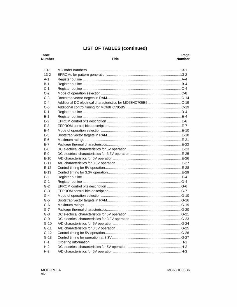
LIST OF TABLESTableNumber
PageNumberTitle
1-1 Data sheet appendices...........................................................................................1-12-1 Mode of operation selection ...................................................................................2-12-2 MC68HC05B6 self-check results............................................................................2-23-1 EEPROM control bits description ...........................................................................3-43-2 Register outline.......................................................................................................3-83-3 IRQ sensitivity.........................................................................................................3-94-1 I/O pin states ..........................................................................................................4-26-1 Method of receiver wake-up ...................................................................................6-116-2 SCI clock on SCLK pin ...........................................................................................6-136-3 First prescaler stage ...............................................................................................6-186-4 Second prescaler stage (transmitter) .....................................................................6-186-5 Second prescaler stage (receiver)..........................................................................6-196-6 SCI baud rate selection ..........................................................................................6-208-1 A/D clock selection .................................................................................................8-48-2 A/D channel assignment.........................................................................................8-59-1 Effect of RESET, POR, STOP and WAIT................................................................9-59-2 Interrupt priorities ...................................................................................................9-79-3 IRQ sensitivity.........................................................................................................9-910-1 MUL instruction.....................................................................................................10-510-2 Register/memory instructions...............................................................................10-510-3 Branch instructions ...............................................................................................10-610-4 Bit manipulation instructions.................................................................................10-610-5 Read/modify/write instructions .............................................................................10-710-6 Control instructions...............................................................................................10-710-7 Instruction set (1 of 2)...........................................................................................10-810-8 Instruction set (2 of 2)...........................................................................................10-910-9 M68HC05 opcode map.........................................................................................10-1011-1 Maximum ratings ..................................................................................................11-111-2 Package thermal characteristics...........................................................................11-211-3 DC electrical characteristics for 5V operation.......................................................11-311-4 DC electrical characteristics for 3.3V operation....................................................11-611-5 A/D characteristics for 5V operation .....................................................................11-911-6 A/D characteristics for 3.3V operation ..................................................................11-1011-7 Control timing for 5V operation .............................................................................11-1111-8 Control timing for 3.3V operation ..........................................................................11-12
MOTOROLAxiv
MC68HC05B6
LIST OF TABLES (continued)TableNumber
PageNumberTitle
13-1 MC order numbers ...............................................................................................13-113-2 EPROMs for pattern generation ...........................................................................13-2A-1 Register outline ......................................................................................................A-4B-1 Register outline ......................................................................................................B-4C-1 Register outline ..................................................................................................... C-4C-2 Mode of operation selection .................................................................................. C-8C-3 Bootstrap vector targets in RAM............................................................................ C-14C-4 Additional DC electrical characteristics for MC68HC705B5.................................. C-19C-5 Additional control timing for MC68HC705B5......................................................... C-19D-1 Register outline ..................................................................................................... D-4E-1 Register outline ......................................................................................................E-4E-2 EPROM control bits description .............................................................................E-6E-3 EEPROM control bits description ...........................................................................E-7E-4 Mode of operation selection ...................................................................................E-10E-5 Bootstrap vector targets in RAM.............................................................................E-18E-6 Maximum ratings ....................................................................................................E-21E-7 Package thermal characteristics.............................................................................E-22E-8 DC electrical characteristics for 5V operation ........................................................E-23E-9 DC electrical characteristics for 3.3V operation .....................................................E-25E-10 A/D characteristics for 5V operation .......................................................................E-26E-11 A/D characteristics for 3.3V operation ....................................................................E-27E-12 Control timing for 5V operation...............................................................................E-28E-13 Control timing for 3.3V operation............................................................................E-29F-1 Register outline ......................................................................................................F-4G-1 Register outline ..................................................................................................... G-4G-2 EPROM control bits description ............................................................................ G-6G-3 EEPROM control bits description .......................................................................... G-7G-4 Mode of operation selection .................................................................................. G-10G-5 Bootstrap vector targets in RAM............................................................................ G-16G-6 Maximum ratings ................................................................................................... G-19G-7 Package thermal characteristics............................................................................ G-20G-8 DC electrical characteristics for 5V operation ....................................................... G-21G-9 DC electrical characteristics for 3.3V operation .................................................... G-23G-10 A/D characteristics for 5V operation ...................................................................... G-24G-11 A/D characteristics for 3.3V operation ................................................................... G-25G-12 Control timing for 5V operation.............................................................................. G-26G-13 Control timing for operation at 3.3V....................................................................... G-27H-1 Ordering information.............................................................................................. H-1H-2 DC electrical characteristics for 5V operation ....................................................... H-2H-3 A/D characteristics for 5V operation ...................................................................... H-3
MC68HC05B6 MOTOROLA1-1
INTRODUCTION
1
1INTRODUCTION
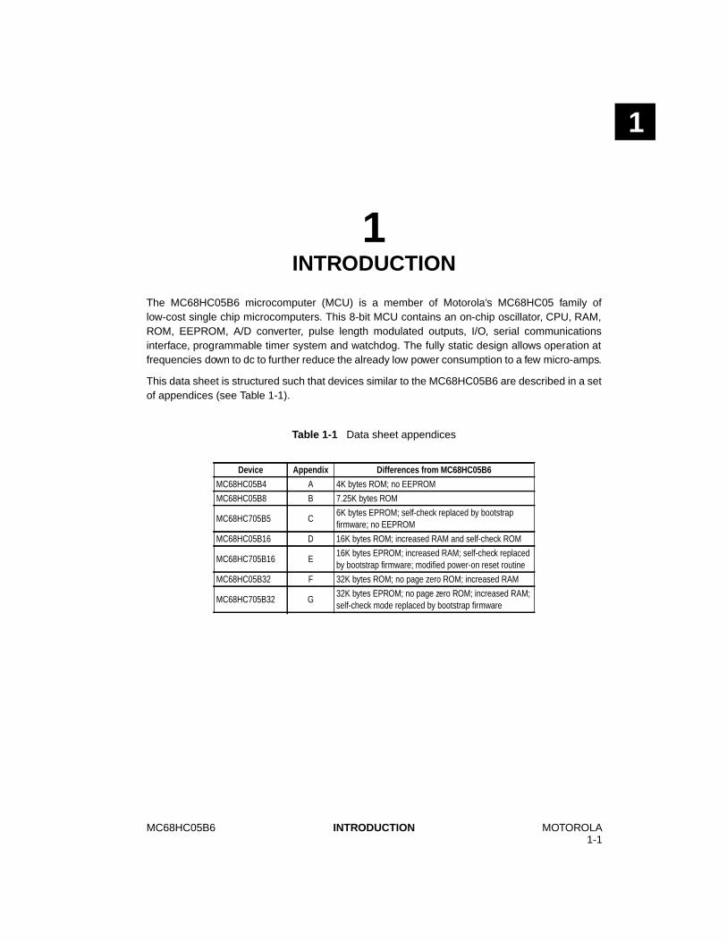
The MC68HC05B6 microcomputer (MCU) is a member of Motorola’s MC68HC05 family oflow-cost single chip microcomputers. This 8-bit MCU contains an on-chip oscillator, CPU, RAM,ROM, EEPROM, A/D converter, pulse length modulated outputs, I/O, serial communicationsinterface, programmable timer system and watchdog. The fully static design allows operation atfrequencies down to dc to further reduce the already low power consumption to a few micro-amps.
This data sheet is structured such that devices similar to the MC68HC05B6 are described in a setof appendices (see Table 1-1).
Table 1-1 Data sheet appendices
Device Appendix Differences from MC68HC05B6
MC68HC05B4 A 4K bytes ROM; no EEPROM
MC68HC05B8 B 7.25K bytes ROM
MC68HC705B5 C6K bytes EPROM; self-check replaced by bootstrapfirmware; no EEPROM
MC68HC05B16 D 16K bytes ROM; increased RAM and self-check ROM
MC68HC705B16 E16K bytes EPROM; increased RAM; self-check replacedby bootstrap firmware; modified power-on reset routine
MC68HC05B32 F 32K bytes ROM; no page zero ROM; increased RAM
MC68HC705B32 G32K bytes EPROM; no page zero ROM; increased RAM;self-check mode replaced by bootstrap firmware
MOTOROLA1-2
MC68HC05B6INTRODUCTION
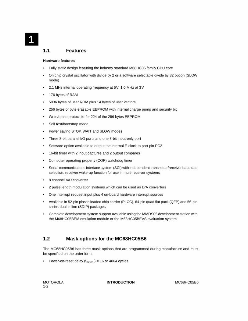
11.1 Features
Hardware features
• Fully static design featuring the industry standard M68HC05 family CPU core
• On chip crystal oscillator with divide by 2 or a software selectable divide by 32 option (SLOWmode)
• 2.1 MHz internal operating frequency at 5V; 1.0 MHz at 3V
• 176 bytes of RAM
• 5936 bytes of user ROM plus 14 bytes of user vectors
• 256 bytes of byte erasable EEPROM with internal charge pump and security bit
• Write/erase protect bit for 224 of the 256 bytes EEPROM
• Self test/bootstrap mode
• Power saving STOP, WAIT and SLOW modes
• Three 8-bit parallel I/O ports and one 8-bit input-only port
• Software option available to output the internal E-clock to port pin PC2
• 16-bit timer with 2 input captures and 2 output compares
• Computer operating properly (COP) watchdog timer
• Serial communications interface system (SCI) with independent transmitter/receiver baud rateselection; receiver wake-up function for use in multi-receiver systems
• 8 channel A/D converter
• 2 pulse length modulation systems which can be used as D/A converters
• One interrupt request input plus 4 on-board hardware interrupt sources
• Available in 52-pin plastic leaded chip carrier (PLCC), 64-pin quad flat pack (QFP) and 56-pinshrink dual in line (SDIP) packages
• Complete development system support available using the MMDS05 development station withthe M68HC05BEM emulation module or the M68HC05BEVS evaluation system
1.2 Mask options for the MC68HC05B6
The MC68HC05B6 has three mask options that are programmed during manufacture and mustbe specified on the order form.
• Power-on-reset delay (tPORL) = 16 or 4064 cycles
MC68HC05B6 MOTOROLA1-3
INTRODUCTION
1• Automatic watchdog enable/disable following a power-on or external reset
• Watchdog enable/disable during WAIT mode
Warning: It is recommended that an external clock is always used if tPORL is set to 16 cycles. Thiswill prevent any problems arising with oscillator stability when the device is put intoSTOP mode.
Figure 1-1 MC68HC05B6 block diagram
Port
A
PA0PA1PA2PA3PA4PA5PA6PA7
Port
B
PB0PB1PB2PB3PB4PB5PB6PB7
Port
C
PC0PC1PC2/ECLKPC3PC4PC5PC6PC7
16-bitprogrammable
timer
Port
D
PD0/AN0PD1/AN1PD2/AN2PD3/AN3PD4/AN4PD5/AN5PD6/AN6PD7/AN7
Oscillator
176 bytesRAM
COP watchdogRESET
IRQ
VDDVSS
OSC1OSC2
M68HC05CPU
SCIA/D converter
PLM
TCAP1TCAP2
TCMP1TCMP2
VRHVRL
RDISCLKTDO
VPP1
256 bytesEEPROM
Charge pump
2 / 32
PLMA D/APLMB D/A
8-bit
432 bytes
User ROM5950 bytes
self check ROM
(including 14 bytesUser vectors)

MOTOROLA1-4
MC68HC05B6INTRODUCTION
THIS PAGE INTENTIONALLY LEFT BLANK
1
MC68HC05B6 MOTOROLA2-1
MODES OF OPERATION AND PIN DESCRIPTIONS
2
2MODES OF OPERATION AND PIN
DESCRIPTIONS
2.1 Modes of operation
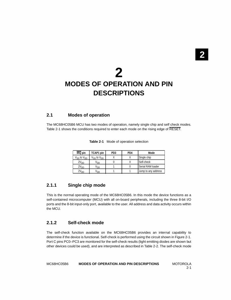
The MC68HC05B6 MCU has two modes of operation, namely single chip and self check modes.Table 2-1 shows the conditions required to enter each mode on the rising edge of RESET.
2.1.1 Single chip mode
This is the normal operating mode of the MC68HC05B6. In this mode the device functions as aself-contained microcomputer (MCU) with all on-board peripherals, including the three 8-bit I/Oports and the 8-bit input-only port, available to the user. All address and data activity occurs withinthe MCU.
2.1.2 Self-check mode
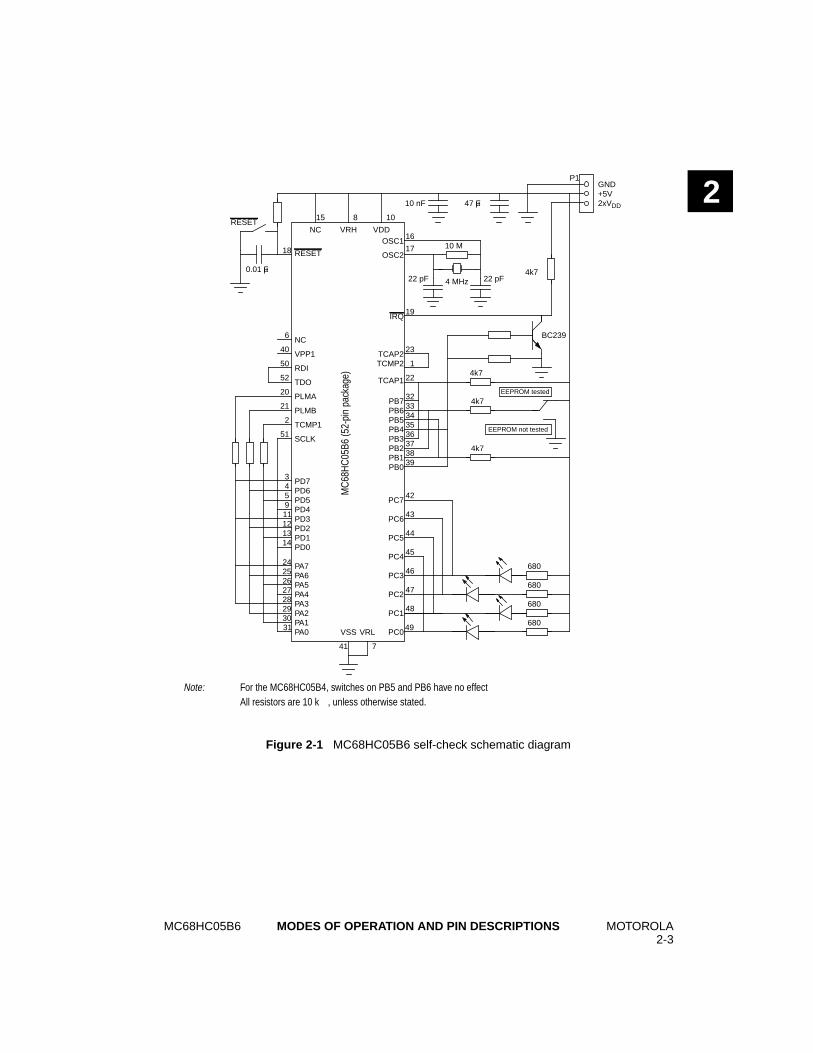
The self-check function available on the MC68HC05B6 provides an internal capability todetermine if the device is functional. Self-check is performed using the circuit shown in Figure 2-1.Port C pins PC0–PC3 are monitored for the self-check results (light emitting diodes are shown butother devices could be used), and are interpreted as described in Table 2-2. The self-check mode
Table 2-1 Mode of operation selection
IRQ pin TCAP1 pin PD3 PD4 Mode
VSS to VDD VSS to VDD X X Single chip
2VDD VDD 0 X Self-check
2VDD VDD 1 0 Serial RAM loader
2VDD VDD 1 1 Jump to any address
MOTOROLA2-2
MC68HC05B6MODES OF OPERATION AND PIN DESCRIPTIONS
2is entered by applying 2 x VDD dc (via a 4.7k½ resistor) to theIRQ pin and 5V dc input (via a 4.7k½resistor) to the TCAP1 pin and then depressing the reset switch to execute a reset. After reset, thefollowing tests are performed automatically and once completed they continually repeat. A gooddevice will exhibit flashing LEDs; a bad device will be indicated by the LEDs holding at one value.
I/0 — Functionally exercises ports A, B, C and D
RAM — Counter test for each RAM byte
ROM — Exclusive OR with odd ones parity result
Timer — Tracks counter registers and checks ICF1, ICF2, OCF1,OCF2 and TOF flags
SCI — Transmission test; check for RDRF, TDRE, TC and FEflags
A/D — Check A/D functionality on internal channels: VRL, VRHand (VRL + VRH)/2
EEPROM — This test is optional; it executes a write/erase test of the256 bytes EEPROM (available only for the MC68HC05B6version), and then deactivates the security bit.
PLM — Checks the PLM basic functionality
Interrupts — Tests external timer and SCI interrupts
Watchdog — Tests the watchdog
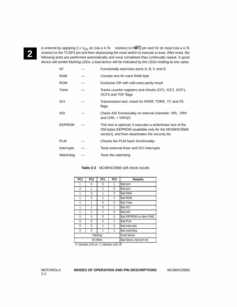
Table 2-2 MC68HC05B6 self-check results
PC3 PC2 PC1 PC0 Remarks
1 0 0 1 Bad port
0 1 1 0 Bad port
1 0 1 0 Bad RAM
1 0 1 1 Bad ROM
1 1 0 0 Bad Timer
1 1 0 1 Bad SCI
1 1 1 0 Bad A/D
0 0 0 0 Bad EEPROM (or other if B4)
0 0 0 1 Bad PLM
0 0 1 0 Bad interrupts
0 0 1 1 Bad watchdog
Flashing Good device
All others Bad device, bad port etc.
‘0’ indicates LED on; ‘1’ indicates LED off
MC68HC05B6 MOTOROLA2-3
MODES OF OPERATION AND PIN DESCRIPTIONS
2
Figure 2-1 MC68HC05B6 self-check schematic diagram
6
40
51
OSC1
OSC2
IRQ
TCAP2TCMP2
TCAP1
PB7PB6PB5PB4PB3PB2PB1PB0
PC7
PC6
PC5
PC4
PC3
PC2
PC1
PC0VRLVSS
PD7PD6PD5PD4PD3PD2PD1PD0
PA7PA6PA5PA4PA3PA2PA1PA0
TCMP1
SCLK
PLMB
PLMA
TDO
RDI
VPP1
NC
RESET
NC VRH VDD
18
50
52
20
21
2
345911121314
2425262728293031
16
17
19
23
1
22
3233343536373839
42
43
44
45
46
47
48
49
41 7
0.01 µF
10 nF 47 µF
10 M½
4 MHz22 pF4k7 ½
4k7 ½
680 ½
22 pF
4k7 ½
4k7 ½
680 ½
680 ½
680 ½
BC239
P1GND+5V2xVDD
RESET
EEPROM tested
EEPROM not tested
15 8 10
Note: For the MC68HC05B4, switches on PB5 and PB6 have no effectAll resistors are 10 k½, unless otherwise stated.
MC
68H
C05
B6 (5
2-pi
n pa
ckag
e)
MOTOROLA2-4
MC68HC05B6MODES OF OPERATION AND PIN DESCRIPTIONS
22.2 Serial RAM loader
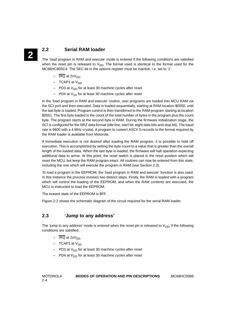
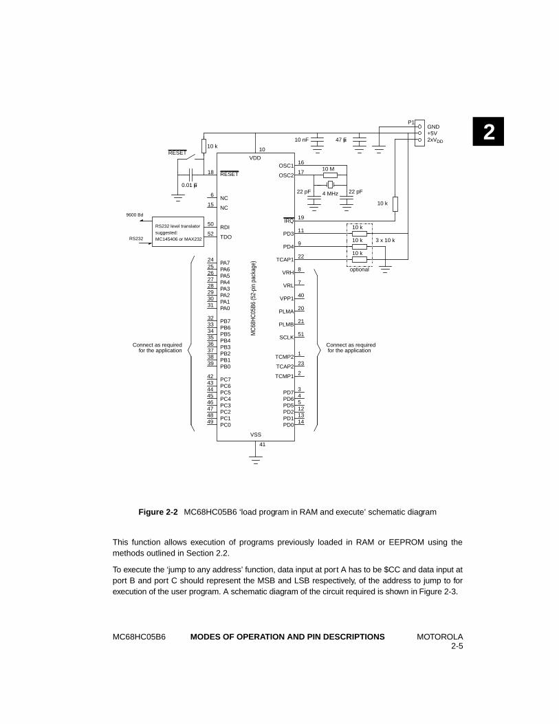
The ‘load program in RAM and execute’ mode is entered if the following conditions are satisfiedwhen the reset pin is released to VDD. The format used is identical to the format used for theMC68HC805C4. The SEC bit in the options register must be inactive, i.e. set to ‘1’.
– IRQ at 2xVDD
– TCAP1 at VDD
– PD3 at VDD for at least 30 machine cycles after reset
– PD4 at VSS for at least 30 machine cycles after reset
In the ‘load program in RAM and execute’ routine, user programs are loaded into MCU RAM viathe SCI port and then executed. Data is loaded sequentially, starting at RAM location $0050, untilthe last byte is loaded. Program control is then transferred to the RAM program starting at location$0051. The first byte loaded is the count of the total number of bytes in the program plus the countbyte. The program starts at the second byte in RAM. During the firmware initialization stage, theSCI is configured for the NRZ data format (idle line, start bit, eight data bits and stop bit). The baudrate is 9600 with a 4 MHz crystal. A program to convert ASCII S-records to the format required bythe RAM loader is available from Motorola.
If immediate execution is not desired after loading the RAM program, it is possible to hold offexecution. This is accomplished by setting the byte count to a value that is greater than the overalllength of the loaded data. When the last byte is loaded, the firmware will halt operation expectingadditional data to arrive. At this point, the reset switch is placed in the reset position which willreset the MCU, but keep the RAM program intact. All routines can now be entered from this state,including the one which will execute the program in RAM (see Section 2.3).
To load a program in the EEPROM, the ‘load program in RAM and execute’ function is also used.In this instance the process involves two distinct steps. Firstly, the RAM is loaded with a programwhich will control the loading of the EEPROM, and when the RAM contents are executed, theMCU is instructed to load the EEPROM.
The erased state of the EEPROM is $FF.
Figure 2-2 shows the schematic diagram of the circuit required for the serial RAM loader.
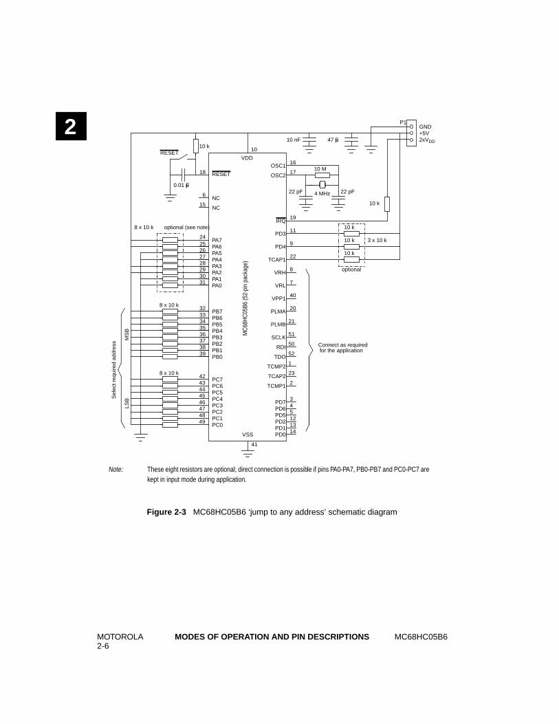
2.3 ‘Jump to any address’
The ‘jump to any address’ mode is entered when the reset pin is released to VDD, if the followingconditions are satisfied:
– IRQ at 2xVDD
– TCAP1 at VDD
– PD3 at VDD for at least 30 machine cycles after reset
– PD4 at VDD for at least 30 machine cycles after reset
MC68HC05B6 MOTOROLA2-5
MODES OF OPERATION AND PIN DESCRIPTIONS
2
This function allows execution of programs previously loaded in RAM or EEPROM using themethods outlined in Section 2.2.
To execute the ‘jump to any address’ function, data input at port A has to be $CC and data input atport B and port C should represent the MSB and LSB respectively, of the address to jump to forexecution of the user program. A schematic diagram of the circuit required is shown in Figure 2-3.
Figure 2-2 MC68HC05B6 ‘load program in RAM and execute’ schematic diagram
32
OSC1
OSC2
IRQ
TCAP2
TCMP2
TCAP1
PB7PB6PB5PB4PB3PB2PB1PB0
PC7PC6PC5PC4PC3PC2PC1PC0
VSS
PD7PD6PD5
PD4
PD3
PD2PD1PD0
PA7PA6PA5PA4PA3PA2PA1PA0
RESET
VDD
18
2425262728293031
16
17
19
41
10 k½
0.01 µF
10 nF 47 µF
10 M½
4 MHz22 pF
10 k½
22 pF
P1GND+5V2xVDD
RESET10
VRH
VRL
VPP1
PLMA
PLMB
TCMP1
RDI
TDO
NC
NC
RS232 level translatorsuggested:MC145406 or MAX232
9600 Bd
RS232
SCLK
10 k½
10 k½
10 k½
11
9
22
8
7
40
20
21
51
1
23
2
345121314
33343536373839
4243444546474849
6
15
50
52
optional
3 x 10 k½
Connect as required for the application
Connect as required for the application
MC
68H
C05
B6 (5
2-pi
n pa
ckag
e)
MOTOROLA2-6
MC68HC05B6MODES OF OPERATION AND PIN DESCRIPTIONS
2
Figure 2-3 MC68HC05B6 ‘jump to any address’ schematic diagram
32
OSC1
OSC2
IRQ
TCAP2
TCMP2
TCAP1
PB7PB6PB5PB4PB3PB2PB1PB0
PC7PC6PC5PC4PC3PC2PC1PC0
VSS
PD7PD6PD5
PD4
PD3
PD2PD1PD0
PA7PA6PA5PA4PA3PA2PA1PA0
RESET
VDD
18
2425262728293031
16
17
19
41
10 k½
0.01 µF
10 nF 47 µF
10 M½
4 MHz22 pF
10 k½
22 pF
P1GND+5V2xVDD
RESET10
VRH
VRL
VPP1
PLMA
PLMB
TCMP1
RDI
TDO
NC
NC
SCLK
10 k½
10 k½
10 k½
11
9
22
8
7
40
20
21
51
1
23
2
345121314
33343536373839
4243444546474849
6
15
50
52
optional
3 x 10 k½
Connect as required for the application
8 x 10 k½ optional (see note)
8 x 10 k½
8 x 10 k½
MS
BLS
BSel
ect r
equi
red
addr
ess
Note: These eight resistors are optional; direct connection is possible if pins PA0-PA7, PB0-PB7 and PC0-PC7 arekept in input mode during application.
MC
68H
C05
B6 (5
2-pi
n pa
ckag
e)
MC68HC05B6 MOTOROLA2-7
MODES OF OPERATION AND PIN DESCRIPTIONS
22.4 Low power modes
The STOP and WAIT instructions have different effects on the programmable timer, the serialcommunications interface, the watchdog system, the EEPROM and the A/D converter. Thesedifferent effects are described in the following sections.
2.4.1 STOP
The STOP instruction places the MCU in its lowest power consumption mode. In STOP mode, theinternal oscillator is turned off, halting all internal processing including timer, serialcommunications interface and the A/D converter (see flowchart in Figure 2-4). The only way forthe MCU to wake-up from the STOP mode is by receipt of an external interrupt or by the detectionof a reset (logic low on RESET pin or a power-on reset).
During STOP mode, the I-bit in the CCR is cleared to enable external interrupts (see Section10.1.5). The SM bit is cleared to allow nominal speed operation for the 4064 cycles count whileexiting STOP mode (see Section 2.4.3).
All other registers and memory remain unaltered and all input/output lines remain unchanged.This continues until an external interrupt (IRQ) or reset is sensed, at which time the internaloscillator is turned on. The external interrupt or reset causes the program counter to vector to thecorresponding locations ($1FFA, B and $1FFE, F respectively).
When leaving STOP mode, a tPORL internal cycles delay is provided to give the oscillator time tostabilise before releasing CPU operation. This delay is selectable via a mask option to be either16 or 4064 cycles. The CPU will resume operation by servicing the interrupt that wakes it up, orby fetching the reset vector, if reset wakes it up.
Warning: If tPORL is selected to be 16 cycles, it is recommended that an external clock signal isused to avoid problems with oscillator stability while the device is in STOP mode.
Note: The stacking corresponding to an eventual interrupt to go out of STOP mode will onlybe executed when going out of STOP mode.
The following list summarizes the effect of STOP mode on the individual modules of theMC68HC05B6.
– The watchdog timer is reset; refer to Section 9.1.4.1
– The EEPROM acts as read-only memory (ROM); refer to Section 3.6
– All SCI activity stopped; refer to Section 6.13
– The timer stops counting; refer to Section 5.6
– The PLM outputs remain at current level; refer to Section 7.2
– The A/D converter is disabled; refer to Section 8.3
– The I-bit in the CCR is cleared
MOTOROLA2-8
MC68HC05B6MODES OF OPERATION AND PIN DESCRIPTIONS
2
Figure 2-4 STOP and WAIT flowcharts
Timer interrupt?
IRQexternal
interrupt?
SCI interrupt?
Stop oscillator and allclocks.
Clear I bit.
STOP WAIT
Reset?
IRQexternal
interrupt?
Generate watchdoginterrupt
Reset?
Watchdog active?
(1) Fetch reset vector or(2) Service interrupt:
a. stackb. set I-bitc. vector to interrupt
routine
(1) Fetch reset vector or(2) Service interrupt:
a. stackb. set I-bitc. vector to interrupt
routine
Turn on oscillator. Wait for time delay to
stabiliseRestart processor clock
YES
NO
YES
YES
YES
YES
YES
YES
NO
NO
NO
NO
NO
NO
Oscillator active. Timer, SCI,A/D, EEPROM clocks active.
Processor clocks stoppedClear I-bit
MC68HC05B6 MOTOROLA2-9
MODES OF OPERATION AND PIN DESCRIPTIONS
22.4.2 WAIT
The WAIT instruction places the MCU in a low power consumption mode, but WAIT modeconsumes more power than STOP mode. All CPU action is suspended and the watchdog isdisabled, but the timer, A/D and SCI systems remain active and operate as normal (see flowchartin Figure 2-4). All other memory and registers remain unaltered and all parallel input/output linesremain unchanged. The programming or erase mechanism of the EEPROM is also unaffected, aswell as the charge pump high voltage generator.
During WAIT mode the I-bit in the CCR is cleared to enable all interrupts. The INTE bit in themiscellaneous register (Section 2.5) is not affected by WAIT mode. When any interrupt or reset issensed, the program counter vectors to the locations containing the start address of the interruptor reset service routine.
Any IRQ, timer (overflow, input capture or output compare) or SCI interrupt (in addition to a logiclow on the RESET pin) causes the processor to exit WAIT mode.
If a non-reset exit from WAIT mode is performed (i.e. timer overflow interrupt exit), the state of theremaining systems will be unchanged.
If a reset exit from WAIT mode is performed the entire system reverts to the disabled reset state.
Note: The stacking corresponding to an eventual interrupt to leave WAIT mode will only beexecuted when leaving WAIT mode.
The following list summarizes the effect of WAIT mode on the modules of the MC68HC05B6.
– The watchdog timer functions according to the mask option selected; referto Section 9.1.4.2
– The EEPROM is not affected; refer to Section 3.7
– The SCI is not affected; refer to Section 6.14
– The timer is not affected; refer to Section 5.7
– The PLM is not affected; refer to Section 7.4
– The A/D converter is not affected; refer to Section 8.4
– The I-bit in the CCR is cleared
2.4.2.1 Power consumption during WAIT mode
Power consumption during WAIT mode depends on how many systems are active. The powerconsumption will be highest when all the systems (A/D, timer, EEPROM and SCI) are active, andlowest when the EEPROM erase and programming mechanism, SCI and A/D are disabled. Thetimer cannot be disabled in WAIT mode. It is important that before entering WAIT mode, theprogrammer sets the relevant control bits for the individual modules to reflect the desiredfunctionality during WAIT mode.
Power consumption may be further reduced by the use of SLOW mode.
MOTOROLA2-10
MC68HC05B6MODES OF OPERATION AND PIN DESCRIPTIONS
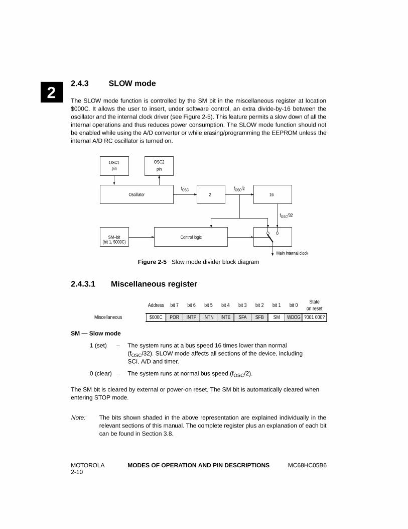
22.4.3 SLOW mode
The SLOW mode function is controlled by the SM bit in the miscellaneous register at location$000C. It allows the user to insert, under software control, an extra divide-by-16 between theoscillator and the internal clock driver (see Figure 2-5). This feature permits a slow down of all theinternal operations and thus reduces power consumption. The SLOW mode function should notbe enabled while using the A/D converter or while erasing/programming the EEPROM unless theinternal A/D RC oscillator is turned on.
2.4.3.1 Miscellaneous register
SM — Slow mode
1 (set) – The system runs at a bus speed 16 times lower than normal(fOSC/32). SLOW mode affects all sections of the device, includingSCI, A/D and timer.
0 (clear) – The system runs at normal bus speed (fOSC/2).
The SM bit is cleared by external or power-on reset. The SM bit is automatically cleared whenentering STOP mode.
Note: The bits shown shaded in the above representation are explained individually in therelevant sections of this manual. The complete register plus an explanation of each bitcan be found in Section 3.8.
Figure 2-5 Slow mode divider block diagram
Address bit 7 bit 6 bit 5 bit 4 bit 3 bit 2 bit 1 bit 0State
on reset
Miscellaneous $000C POR INTP INTN INTE SFA SFB SM WDOG ?001 000?
OSC1pin
OSC2
pin
OscillatorfOSC
Control logicSM–bit
fOSC/2 2 16
Main internal clock
fOSC/32
(bit 1, $000C)
MC68HC05B6 MOTOROLA2-11
MODES OF OPERATION AND PIN DESCRIPTIONS
22.5 Pin descriptions
2.5.1 VDD and VSS
Power is supplied to the microcontroller using these two pins. VDD is the positive supply and VSSis ground.
It is in the nature of CMOS designs that very fast signal transitions occur on the MCU pins. Theseshort rise and fall times place very high short-duration current demands on the power supply. Toprevent noise problems, special care must be taken to provide good power supply by-passing atthe MCU. By-pass capacitors should have good high-frequency characteristics and be as close tothe MCU as possible. Bypassing requirements vary, depending on how heavily the MCU pins areloaded.
2.5.2 IRQ
This is an input-only pin for external interrupt sources. Interrupt triggering is selected using theINTP and INTN bits in the miscellaneous register, to be one of four options detailed in Table 9-3.In addition, the external interrupt facility (IRQ) can be disabled using the INTE bit in themiscellaneous register (see Section 3.8). It is only possible to change the interrupt option bits inthe miscellaneous register while the I-bit is set. Selecting a different interrupt option willautomatically clear any pending interrupts. Further details of the external interrupt procedure canbe found in Section 9.2.3.1.
The IRQ pin contains an internal Schmitt trigger as part of its input to improve noise immunity.
2.5.3 RESET
This active low I/O pin is used to reset the MCU. Applying a logic zero to this pin forces the deviceto a known start-up state. An external RC-circuit can be connected to this pin to generate apower-on-reset (POR) if required. In this case, the time constant must be great enough (at least100ms) to allow the oscillator circuit to stabilise. This input has an internal Schmitt trigger toimprove noise immunity. When a reset condition occurs internally, i.e. from the COP watchdog, theRESET pin provides an active-low open drain output signal that may be used to reset externalhardware.
2.5.4 TCAP1
The TCAP1 input controls the input capture 1 function of the on-chip programmable timer system.
MOTOROLA2-12
MC68HC05B6MODES OF OPERATION AND PIN DESCRIPTIONS
22.5.5 TCAP2
The TCAP2 input controls the input capture 2 function of the on-chip programmable timer system.
2.5.6 TCMP1
The TCMP1 pin is the output of the output compare 1 function of the timer system.
2.5.7 TCMP2
The TCMP2 pin is the output of the output compare 2 function of the timer system.
2.5.8 OSC1, OSC2
These pins provide control input for an on-chip oscillator circuit. A crystal, ceramic resonator orexternal clock signal connected to these pins supplies the oscillator clock. The oscillator frequency(fOSC) is divided by two to give the internal bus frequency (fOP). There is also a software optionwhich introduces an additional divide by 16 into the oscillator clock, giving an internal busfrequency of fOSC/32.
2.5.8.1 Crystal
The circuit shown in Figure 2-6(a) is recommended when using either a crystal or a ceramicresonator. Figure 2-6(d) lists the recommended capacitance and feedback resistance values. Theinternal oscillator is designed to interface with an AT-cut parallel-resonant quartz crystal resonatorin the frequency range specified for fOSC (see Section 11.5). Use of an external CMOS oscillatoris recommended when crystals outside the specified ranges are to be used. The crystal andassociated components should be mounted as close as possible to the input pins to minimiseoutput distortion and start-up stabilisation time. The manufacturer of the particular crystal beingconsidered should be consulted for specific information.
2.5.8.2 Ceramic resonator
A ceramic resonator may be used instead of a crystal in cost sensitive applications. The circuit shownin Figure 2-6(a) is recommended when using either a crystal or a ceramic resonator. Figure 2-6(d) liststhe recommended capacitance and feedback resistance values. The manufacturer of the particularceramic resonator being considered should be consulted for specific information.
MC68HC05B6 MOTOROLA2-13
MODES OF OPERATION AND PIN DESCRIPTIONS
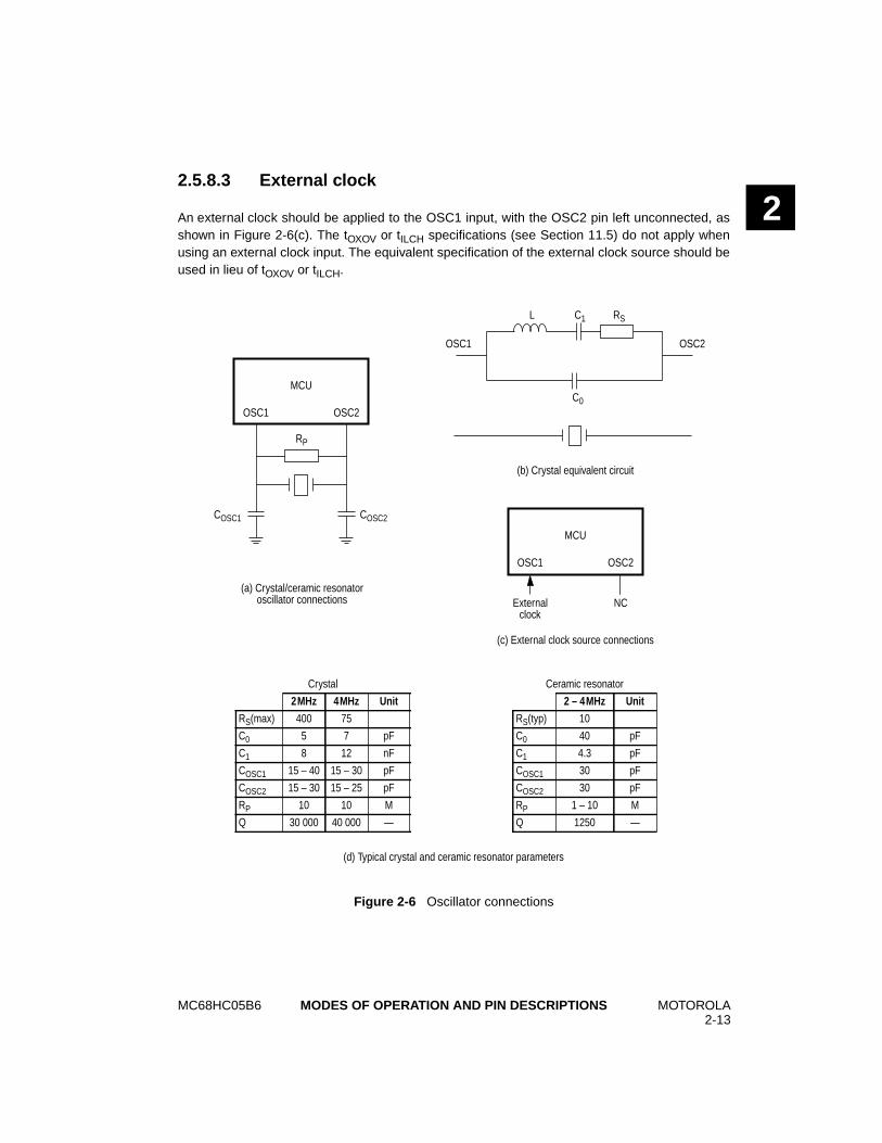
22.5.8.3 External clock
An external clock should be applied to the OSC1 input, with the OSC2 pin left unconnected, asshown in Figure 2-6(c). The tOXOV or tILCH specifications (see Section 11.5) do not apply whenusing an external clock input. The equivalent specification of the external clock source should beused in lieu of tOXOV or tILCH.
Figure 2-6 Oscillator connections
Ceramic resonator
2 – 4MHz Unit
RS(typ) 10
C0 40 pF
C1 4.3 pF
COSC1 30 pF
COSC2 30 pF
RP 1 – 10 M½
Q 1250 —
Crystal
2MHz 4MHz Unit
RS(max) 400 75
C0 5 7 pF
C1 8 12 nF
COSC1 15 – 40 15 – 30 pF
COSC2 15 – 30 15 – 25 pF
RP 10 10 M½
Q 30 000 40 000 —
OSC1 OSC2
RP
MCU
COSC2COSC1
OSC1 OSC2
MCU
NCExternalclock
OSC1 OSC2
RSC1L
C0
(d) Typical crystal and ceramic resonator parameters
(c) External clock source connections
(b) Crystal equivalent circuit
(a) Crystal/ceramic resonatoroscillator connections
MOTOROLA2-14
MC68HC05B6MODES OF OPERATION AND PIN DESCRIPTIONS
22.5.9 RDI (Receive data in)
The RDI pin is the input pin of the SCI receiver.
2.5.10 TDO (Transmit data out)
The TDO pin is the output pin of the SCI transmitter.
2.5.11 SCLK
The SCLK pin is the clock output pin of the SCI transmitter.
2.5.12 PLMA
The PLMA pin is the output of pulse length modulation converter A.
2.5.13 PLMB
The PLMB pin is the output of pulse length modulation converter B.
2.5.14 VPP1
The VPP1 pin is the output of the charge pump for the EEPROM1 array.
2.5.15 VRH
The VRH pin is the positive reference voltage for the A/D converter.
2.5.16 VRL
The VRL pin is the negative reference voltage for the A/D converter.
2.5.17 PA0 – PA7/PB0 – PB7/PC0 – PC7
These 24 I/O lines comprise ports A, B and C. The state of any pin is software programmable, andall the pins are configured as inputs during power-on or reset.
Under software control the PC2 pin can output the internal E-clock (see Section 4.2).
2.5.18 PD0/AN0–PD7/AN7
This 8-bit input only port (D) shares its pins with the A/D converter. When enabled, the A/Dconverter uses pins PD0/AN0 – PD7/AN7 as its analog inputs. On reset, the A/D converter isdisabled which forces the port D pins to be input only port pins (see Section 8.5).
MC68HC05B6 MOTOROLA3-1
MEMORY AND REGISTERS
33MEMORY AND REGISTERS
The MC68HC05B6 MCU is capable of addressing 8192 bytes of memory and registers with itsprogram counter. The memory map includes 5950 bytes of User ROM (including User vectors),432 bytes of self check ROM, 176 bytes of RAM and 256 bytes of EEPROM.
3.1 Registers
All the I/O, control and status registers of the MC68HC05B6 are contained within the first 32-byteblock of the memory map, as shown in Figure 3-1. The miscellaneous register is shown in Section3.8 as this register contains bits which are relevant to several modules.
3.2 RAM
The user RAM comprises 176 bytes of memory, from $0050 to $00FF. This is shared with a 64byte stack area. The stack begins at $00FF and may extend down to $00C0.
Note: Using the stack area for data storage or temporary work locations requires care to preventthe data from being overwritten due to stacking from an interrupt or subroutine call.
3.3 ROM
The User ROM consists of 5950 bytes of ROM mapped as follows:
• 48 bytes of page zero ROM from $0020 to $004F
• 5888 bytes of User ROM from $0800 to $1EFF
• 14 bytes of User vectors from $1FF2 to $1FFF
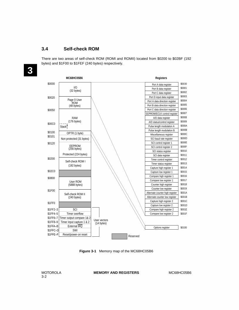
MOTOROLA3-2
MC68HC05B6MEMORY AND REGISTERS
3
3.4 Self-check ROM
There are two areas of self-check ROM (ROMI and ROMII) located from $0200 to $02BF (192bytes) and $1F00 to $1FEF (240 bytes) respectively.
Figure 3-1 Memory map of the MC68HC05B6
$1FFE–F
$1FF6–7
Port B data register
Port C data register
Port D input data register
Port A data register $0000
Compare low register 2
A/D data register
User vectors(14 bytes)
$0000I/O
(32 bytes)
$0020
$00C0
$0100
$1FF0
Stack
RAM(176 bytes)
$02C0
$0200
$1F00
$0050
Port A data direction register
Port B data direction register
Port C data direction register
EEPROM/ECLK control register
A/D status/control register
Pulse length modulation A
Pulse length modulation B
Miscellaneous register
SCI baud rate register
SCI control register 1
SCI control register 2
SCI status register
SCI data register
Timer control register
Timer status register
Capture high register 1
Capture low register 1
Compare high register 1
Compare low register 1
Counter high register
Counter low register
Alternate counter high register
Alternate counter low register
Capture high register 2
Capture low register 2
Compare high register 2
$0001
$0002
$0003
$0004
$0005
$0006
$0007
$0008
$0009
$000A
$000B
$000C
$000D
$000E
$000F
$0010
$0011
$0012
$0013
$0014
$0015
$0016
$0017
$0018
$0019
$001A
$001B
$001C
$001D
$001E
$001F
Page 0 UserROM
(48 bytes)
Self-check ROM I(192 bytes)
User ROM(5888 bytes)
Self-check ROM II(240 bytes)
$0800
$1FF2–3
OPTR (1 byte)
Non protected (31 bytes)
Protected (224 bytes)
EEPROM(256 bytes)
$0101
$0120
$0100Options register
Reserved
MC68HC05B6 Registers
SCITimer overflow
Timer output compare 1& 2Timer input capture 1 & 2
External IRQSWI
Reset/power-on reset
$1FF4–5
$1FF8–9$1FFA–B$1FFC–D
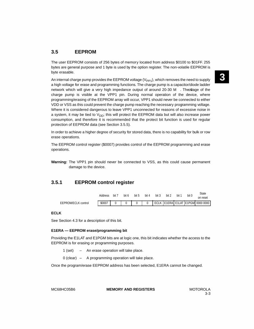
MC68HC05B6 MOTOROLA3-3
MEMORY AND REGISTERS
3
3.5 EEPROM
The user EEPROM consists of 256 bytes of memory located from address $0100 to $01FF. 255bytes are general purpose and 1 byte is used by the option register. The non-volatile EEPROM isbyte erasable.
An internal charge pump provides the EEPROM voltage (VPP1), which removes the need to supplya high voltage for erase and programming functions. The charge pump is a capacitor/diode laddernetwork which will give a very high impedance output of around 20-30 M½. The voltage of thecharge pump is visible at the VPP1 pin. During normal operation of the device, whereprogramming/erasing of the EEPROM array will occur, VPP1 should never be connected to eitherVDD or VSS as this could prevent the charge pump reaching the necessary programming voltage.Where it is considered dangerous to leave VPP1 unconnected for reasons of excessive noise ina system, it may be tied to VDD; this will protect the EEPROM data but will also increase powerconsumption, and therefore it is recommended that the protect bit function is used for regularprotection of EEPROM data (see Section 3.5.5).
In order to achieve a higher degree of security for stored data, there is no capability for bulk or rowerase operations.
The EEPROM control register ($0007) provides control of the EEPROM programming and eraseoperations.
Warning: The VPP1 pin should never be connected to VSS, as this could cause permanentdamage to the device.
3.5.1 EEPROM control register
ECLK
See Section 4.3 for a description of this bit.
E1ERA — EEPROM erase/programming bit
Providing the E1LAT and E1PGM bits are at logic one, this bit indicates whether the access to theEEPROM is for erasing or programming purposes.
1 (set) – An erase operation will take place.
0 (clear) – A programming operation will take place.
Once the program/erase EEPROM address has been selected, E1ERA cannot be changed.
Address bit 7 bit 6 bit 5 bit 4 bit 3 bit 2 bit 1 bit 0State
on reset
EEPROM/ECLK control $0007 0 0 0 0 ECLK E1ERA E1LAT E1PGM 0000 0000
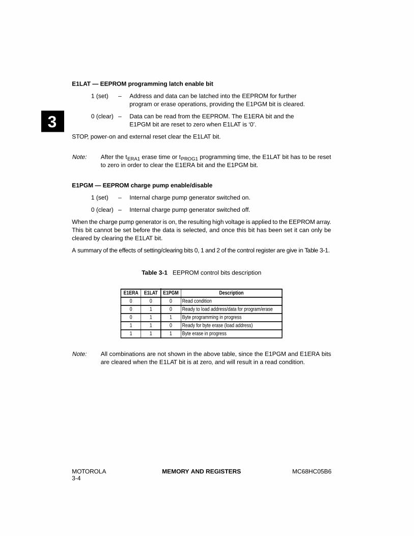
MOTOROLA3-4
MC68HC05B6MEMORY AND REGISTERS
3
E1LAT — EEPROM programming latch enable bit
1 (set) – Address and data can be latched into the EEPROM for furtherprogram or erase operations, providing the E1PGM bit is cleared.
0 (clear) – Data can be read from the EEPROM. The E1ERA bit and theE1PGM bit are reset to zero when E1LAT is ‘0’.
STOP, power-on and external reset clear the E1LAT bit.
Note: After the tERA1 erase time or tPROG1 programming time, the E1LAT bit has to be resetto zero in order to clear the E1ERA bit and the E1PGM bit.
E1PGM — EEPROM charge pump enable/disable
1 (set) – Internal charge pump generator switched on.
0 (clear) – Internal charge pump generator switched off.
When the charge pump generator is on, the resulting high voltage is applied to the EEPROM array.This bit cannot be set before the data is selected, and once this bit has been set it can only becleared by clearing the E1LAT bit.
A summary of the effects of setting/clearing bits 0, 1 and 2 of the control register are give in Table 3-1.
Note: All combinations are not shown in the above table, since the E1PGM and E1ERA bitsare cleared when the E1LAT bit is at zero, and will result in a read condition.
Table 3-1 EEPROM control bits description
E1ERA E1LAT E1PGM Description
0 0 0 Read condition
0 1 0 Ready to load address/data for program/erase
0 1 1 Byte programming in progress
1 1 0 Ready for byte erase (load address)
1 1 1 Byte erase in progress
MC68HC05B6 MOTOROLA3-5
MEMORY AND REGISTERS
3
3.5.2 EEPROM read operation
To be able to read from EEPROM, the E1LAT bit has to be at logic zero, as shown in Table 3-1.While this bit is at logic zero, the E1PGM bit and the E1ERA bit are permanently reset to zero andthe 256 bytes of EEPROM may be read as if it were a normal ROM area. The internal chargepump generator is automatically switched off since the E1PGM bit is reset.
If a read operation is executed while the E1LAT bit is set (erase or programming sequence), dataresulting from the operation will be $FF.
Note: When not performing any programming or erase operation, it is recommended thatEEPROM should remain in the read mode (E1LAT = 0)
3.5.3 EEPROM erase operation
To erase the contents of a byte of the EEPROM, the following steps should be taken:
1 Set the E1LAT bit.
2 Set the E1ERA bit (1& 2 may be done simultaneously with the sameinstruction).
3 Write address/data to the EEPROM address to be erased.
4 Set the E1PGM bit.
5 Wait for a time tERA1.
6 Reset the E1LAT bit (to logic zero).
While an erase operation is being performed, any access of the EEPROM array will not besuccessful.
The erased state of the EEPROM is $FF and the programmed state is $00.
Note: Data written to the address to be erased is not used, therefore its value is notsignificant.
If a second word is to be erased, it is important that the E1LAT bit be reset before restarting theerasing sequence otherwise any write to a new address will have no effect. This condition providesa higher degree of security for the stored data.
User programs must be running from the RAM or ROM as the EEPROM will have its address anddata buses latched.
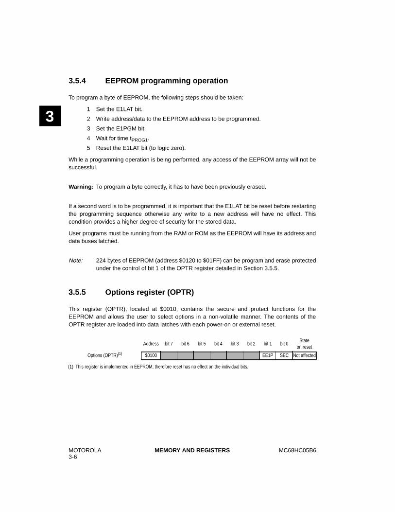
MOTOROLA3-6
MC68HC05B6MEMORY AND REGISTERS
3
3.5.4 EEPROM programming operation
To program a byte of EEPROM, the following steps should be taken:
1 Set the E1LAT bit.
2 Write address/data to the EEPROM address to be programmed.
3 Set the E1PGM bit.
4 Wait for time tPROG1.
5 Reset the E1LAT bit (to logic zero).
While a programming operation is being performed, any access of the EEPROM array will not besuccessful.
Warning: To program a byte correctly, it has to have been previously erased.
If a second word is to be programmed, it is important that the E1LAT bit be reset before restartingthe programming sequence otherwise any write to a new address will have no effect. Thiscondition provides a higher degree of security for the stored data.
User programs must be running from the RAM or ROM as the EEPROM will have its address anddata buses latched.
Note: 224 bytes of EEPROM (address $0120 to $01FF) can be program and erase protectedunder the control of bit 1 of the OPTR register detailed in Section 3.5.5.
3.5.5 Options register (OPTR)
This register (OPTR), located at $0010, contains the secure and protect functions for theEEPROM and allows the user to select options in a non-volatile manner. The contents of theOPTR register are loaded into data latches with each power-on or external reset.
(1) This register is implemented in EEPROM; therefore reset has no effect on the individual bits.
Address bit 7 bit 6 bit 5 bit 4 bit 3 bit 2 bit 1 bit 0State
on reset
Options (OPTR)(1) $0100 EE1P SEC Not affected
MC68HC05B6 MOTOROLA3-7
MEMORY AND REGISTERS
3
EE1P – EEPROM protect bit
In order to achieve a higher degree of protection, the EEPROM is effectively split into two parts,both working from the VPP1 charge pump. Part 1 of the EEPROM array (32 bytes from $0100 to$011F) cannot be protected; part 2 (224 bytes from $0120 to $01FF) is protected by the EE1P bitof the options register.
1 (set) – Part 2 of the EEPROM array is not protected; all 256 bytes of EEPROMcan be accessed for any read, erase or programming operations
0 (clear) – Part 2 of the EEPROM array is protected; any attempt to erase orprogram a location will be unsuccessful
When this bit is set to 1 (erased), the protection will remain until the next power-on or externalreset. EE1P can only be written to ‘0’ when the ELAT bit in the EEPROM control register is set.
SEC – Security bit
This high security bit allows the user to secure the EEPROM data from external accesses. Whenthe SEC bit is at ‘0’, the EEPROM contents are secured by preventing any entry to test mode. Theonly way to erase the SEC bit to ‘1’ externally is to enter self-check mode, at which time the entireEEPROM contents will be erased. When the SEC bit is changed, its new value will have no effectuntil the next external or power-on reset.
3.6 EEPROM during STOP mode
When entering STOP mode, the EEPROM is automatically set to the read mode and the VPP1high voltage charge pump generator is automatically disabled.
3.7 EEPROM during WAIT mode
The EEPROM is not affected by WAIT mode. Any program/erase operation will continue as innormal operating mode. The charge pump is not affected by WAIT mode, therefore it is possibleto wait the tERA1 erase time or tPROG1 programming time in WAIT mode.
Under normal operating conditions, the charge pump generator is driven by the internal CPUclocks. When the operating frequency is low, e.g. during WAIT mode, the clocking should be doneby the internal A/D RC oscillator. The RC oscillator is enabled by setting the ADRC bit of the A/Dstatus/control register at $0009.
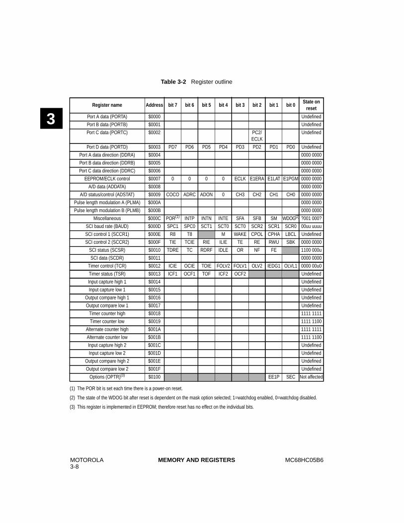
MOTOROLA3-8
MC68HC05B6MEMORY AND REGISTERS
3
(1) The POR bit is set each time there is a power-on reset.
(2) The state of the WDOG bit after reset is dependent on the mask option selected; 1=watchdog enabled, 0=watchdog disabled.
(3) This register is implemented in EEPROM; therefore reset has no effect on the individual bits.
Table 3-2 Register outline
Register name Address bit 7 bit 6 bit 5 bit 4 bit 3 bit 2 bit 1 bit 0State on
reset
Port A data (PORTA) $0000 Undefined
Port B data (PORTB) $0001 Undefined
Port C data (PORTC) $0002 PC2/ECLK
Undefined
Port D data (PORTD) $0003 PD7 PD6 PD5 PD4 PD3 PD2 PD1 PD0 Undefined
Port A data direction (DDRA) $0004 0000 0000
Port B data direction (DDRB) $0005 0000 0000
Port C data direction (DDRC) $0006 0000 0000
EEPROM/ECLK control $0007 0 0 0 0 ECLK E1ERA E1LAT E1PGM 0000 0000
A/D data (ADDATA) $0008 0000 0000
A/D status/control (ADSTAT) $0009 COCO ADRC ADON 0 CH3 CH2 CH1 CH0 0000 0000
Pulse length modulation A (PLMA) $000A 0000 0000
Pulse length modulation B (PLMB) $000B 0000 0000
Miscellaneous $000C POR(1) INTP INTN INTE SFA SFB SM WDOG(2) ?001 000?
SCI baud rate (BAUD) $000D SPC1 SPC0 SCT1 SCT0 SCT0 SCR2 SCR1 SCR0 00uu uuuu
SCI control 1 (SCCR1) $000E R8 T8 M WAKE CPOL CPHA LBCL Undefined
SCI control 2 (SCCR2) $000F TIE TCIE RIE ILIE TE RE RWU SBK 0000 0000
SCI status (SCSR) $0010 TDRE TC RDRF IDLE OR NF FE 1100 000u
SCI data (SCDR) $0011 0000 0000
Timer control (TCR) $0012 ICIE OCIE TOIE FOLV2 FOLV1 OLV2 IEDG1 OLVL1 0000 00u0
Timer status (TSR) $0013 ICF1 OCF1 TOF ICF2 OCF2 Undefined
Input capture high 1 $0014 Undefined
Input capture low 1 $0015 Undefined
Output compare high 1 $0016 Undefined
Output compare low 1 $0017 Undefined
Timer counter high $0018 1111 1111
Timer counter low $0019 1111 1100
Alternate counter high $001A 1111 1111
Alternate counter low $001B 1111 1100
Input capture high 2 $001C Undefined
Input capture low 2 $001D Undefined
Output compare high 2 $001E Undefined
Output compare low 2 $001F Undefined
Options (OPTR)(3) $0100 EE1P SEC Not affected
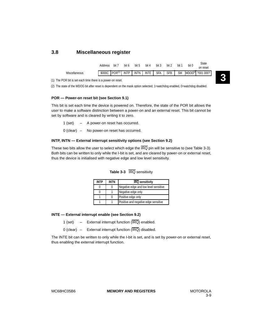
MC68HC05B6 MOTOROLA3-9
MEMORY AND REGISTERS
3
3.8 Miscellaneous register
POR — Power-on reset bit (see Section 9.1)
This bit is set each time the device is powered on. Therefore, the state of the POR bit allows theuser to make a software distinction between a power-on and an external reset. This bit cannot beset by software and is cleared by writing it to zero.
1 (set) – A power-on reset has occurred.
0 (clear) – No power-on reset has occurred.
INTP, INTN — External interrupt sensitivity options (see Section 9.2)
These two bits allow the user to select which edge the IRQ pin will be sensitive to (see Table 3-3).Both bits can be written to only while the I-bit is set, and are cleared by power-on or external reset,thus the device is initialised with negative edge and low level sensitivity.
INTE — External interrupt enable (see Section 9.2)
1 (set) – External interrupt function (IRQ) enabled.
0 (clear) – External interrupt function (IRQ) disabled.
The INTE bit can be written to only while the I-bit is set, and is set by power-on or external reset,thus enabling the external interrupt function.
(1) The POR bit is set each time there is a power-on reset.
(2) The state of the WDOG bit after reset is dependent on the mask option selected; 1=watchdog enabled, 0=watchdog disabled.
Address bit 7 bit 6 bit 5 bit 4 bit 3 bit 2 bit 1 bit 0State
on reset
Miscellaneous $000C POR(1) INTP INTN INTE SFA SFB SM WDOG(2) ?001 000?
Table 3-3 IRQ sensitivity
INTP INTN IRQ sensitivity
0 0 Negative edge and low level sensitive
0 1 Negative edge only
1 0 Positive edge only
1 1 Positive and negative edge sensitive
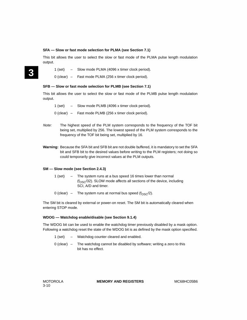
MOTOROLA3-10
MC68HC05B6MEMORY AND REGISTERS
3
SFA — Slow or fast mode selection for PLMA (see Section 7.1)
This bit allows the user to select the slow or fast mode of the PLMA pulse length modulationoutput.
1 (set) – Slow mode PLMA (4096 x timer clock period).
0 (clear) – Fast mode PLMA (256 x timer clock period).
SFB — Slow or fast mode selection for PLMB (see Section 7.1)
This bit allows the user to select the slow or fast mode of the PLMB pulse length modulationoutput.
1 (set) – Slow mode PLMB (4096 x timer clock period).
0 (clear) – Fast mode PLMB (256 x timer clock period).
Note: The highest speed of the PLM system corresponds to the frequency of the TOF bitbeing set, multiplied by 256. The lowest speed of the PLM system corresponds to thefrequency of the TOF bit being set, multiplied by 16.
Warning: Because the SFA bit and SFB bit are not double buffered, it is mandatory to set the SFAbit and SFB bit to the desired values before writing to the PLM registers; not doing socould temporarily give incorrect values at the PLM outputs.
SM — Slow mode (see Section 2.4.3)
1 (set) – The system runs at a bus speed 16 times lower than normal(fOSC/32). SLOW mode affects all sections of the device, includingSCI, A/D and timer.
0 (clear) – The system runs at normal bus speed (fOSC/2).
The SM bit is cleared by external or power-on reset. The SM bit is automatically cleared whenentering STOP mode.
WDOG — Watchdog enable/disable (see Section 9.1.4)
The WDOG bit can be used to enable the watchdog timer previously disabled by a mask option.Following a watchdog reset the state of the WDOG bit is as defined by the mask option specified.
1 (set) – Watchdog counter cleared and enabled.
0 (clear) – The watchdog cannot be disabled by software; writing a zero to thisbit has no effect.
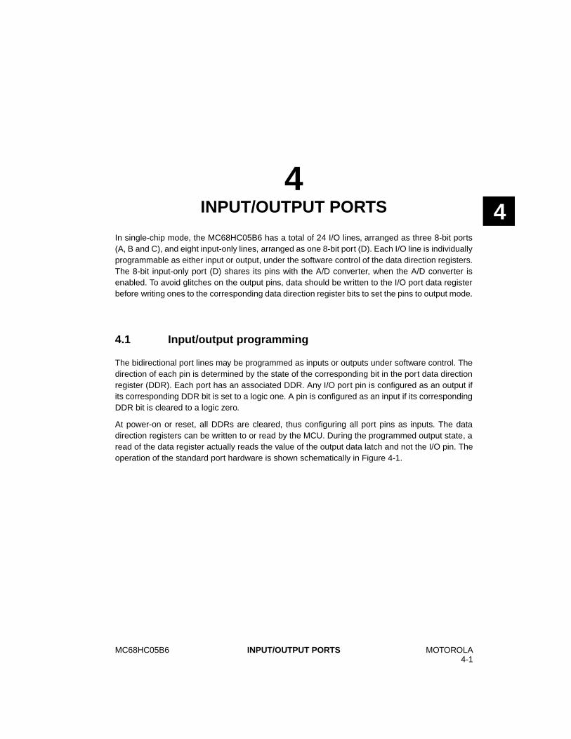
MC68HC05B6 MOTOROLA4-1
INPUT/OUTPUT PORTS
44
INPUT/OUTPUT PORTS
In single-chip mode, the MC68HC05B6 has a total of 24 I/O lines, arranged as three 8-bit ports(A, B and C), and eight input-only lines, arranged as one 8-bit port (D). Each I/O line is individuallyprogrammable as either input or output, under the software control of the data direction registers.The 8-bit input-only port (D) shares its pins with the A/D converter, when the A/D converter isenabled. To avoid glitches on the output pins, data should be written to the I/O port data registerbefore writing ones to the corresponding data direction register bits to set the pins to output mode.
4.1 Input/output programming
The bidirectional port lines may be programmed as inputs or outputs under software control. Thedirection of each pin is determined by the state of the corresponding bit in the port data directionregister (DDR). Each port has an associated DDR. Any I/O port pin is configured as an output ifits corresponding DDR bit is set to a logic one. A pin is configured as an input if its correspondingDDR bit is cleared to a logic zero.
At power-on or reset, all DDRs are cleared, thus configuring all port pins as inputs. The datadirection registers can be written to or read by the MCU. During the programmed output state, aread of the data register actually reads the value of the output data latch and not the I/O pin. Theoperation of the standard port hardware is shown schematically in Figure 4-1.
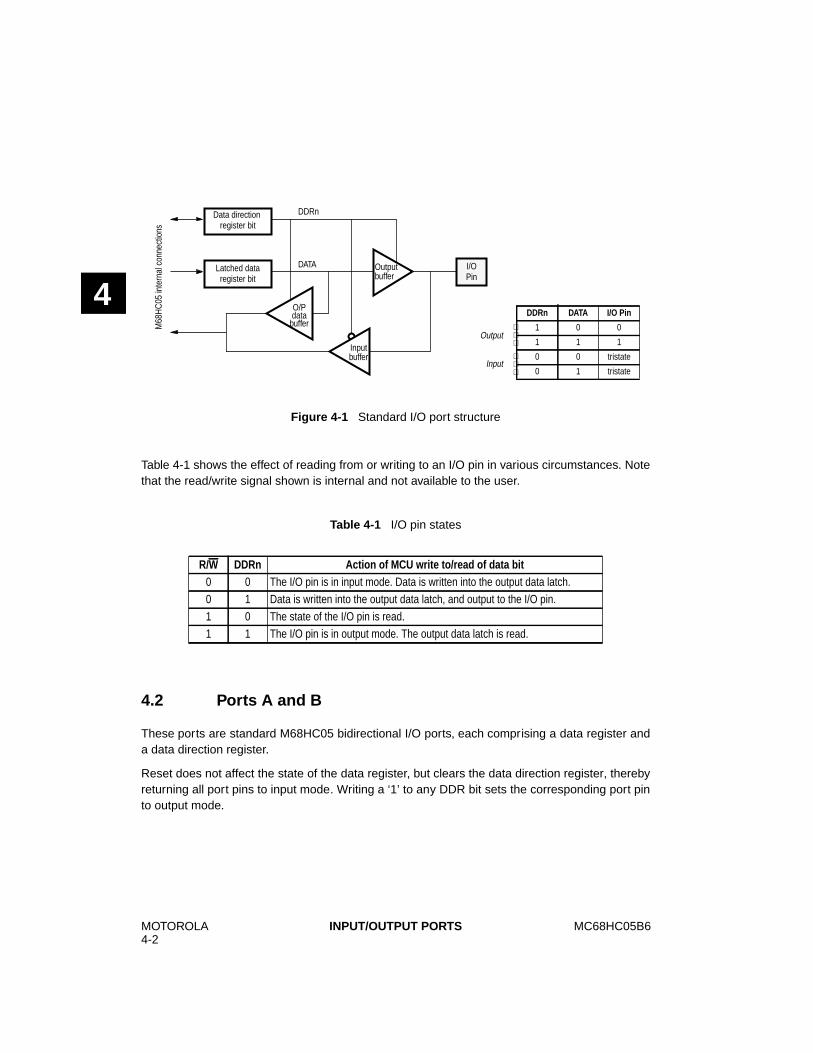
MOTOROLA4-2
MC68HC05B6INPUT/OUTPUT PORTS
4
Table 4-1 shows the effect of reading from or writing to an I/O pin in various circumstances. Notethat the read/write signal shown is internal and not available to the user.
4.2 Ports A and B
These ports are standard M68HC05 bidirectional I/O ports, each comprising a data register anda data direction register.
Reset does not affect the state of the data register, but clears the data direction register, therebyreturning all port pins to input mode. Writing a ‘1’ to any DDR bit sets the corresponding port pinto output mode.
Figure 4-1 Standard I/O port structure
Table 4-1 I/O pin states
R/W DDRn Action of MCU write to/read of data bit0 0 The I/O pin is in input mode. Data is written into the output data latch.0 1 Data is written into the output data latch, and output to the I/O pin.1 0 The state of the I/O pin is read.1 1 The I/O pin is in output mode. The output data latch is read.
Latched dataregister bit
DDRn
DATA
Inputbuffer
Outputbuffer
O/Pdata
bufferM68
HC
05 in
tern
al c
onne
ctio
ns
DDRn DATA I/O Pin
1 0 0
1 1 1
0 0 tristate
0 1 tristate
I/OPin
Output
Input
Data directionregister bit
MC68HC05B6 MOTOROLA4-3
INPUT/OUTPUT PORTS
4
4.3 Port C
In addition to the standard port functions described for port A and B, port C pin 2 can beconfigured, using the ECLK bit of the EEPROM/ECLK control register, to output the CPU clock. Ifthis is selected the corresponding DDR bit is automatically set and bit 2 of port C will always readthe output data latch. The other port C pins are not affected by this feature.
ECLK — External clock output bit
1 (set) – ECLK CPU clock is output on PC2.
0 (clear) – ECLK CPU clock is not output on PC2; port C acts as a normal I/O port.
The ECLK bit is cleared by power-on or external reset. It is not affected by the execution of a STOPor WAIT instruction.
The timing diagram of the clock output is shown in Figure 4-2.
4.4 Port D
This 8-bit input-only port shares its pins with the A/D converter subsystem. When the A/Dconverter is enabled, pins PD0-PD7 read the eight analog inputs to the A/D converter. Port D canbe read at any time, however, if it is read during an A/D conversion sequence noise, may beinjected on the analog inputs, resulting in reduced accuracy of the A/D. Furthermore, performing
Address bit 7 bit 6 bit 5 bit 4 bit 3 bit 2 bit 1 bit 0State
on reset
EEPROM/ECLK control $0007 0 0 0 0 ECLK E1ERA E1LAT E1PGM 0000 0000
Figure 4-2 ECLK timing diagram
Internal clock (PHI2)
External clock (ECLK/PC2)
Output port (if write to output port)
MOTOROLA4-4
MC68HC05B6INPUT/OUTPUT PORTS
4
a digital read of port D with levels other than VDD or VSS on the port D pins will result in greaterpower dissipation during the read cycle.
As port D is an input-only port there is no DDR associated with it. Also, at power up or externalreset, the A/D converter is disabled, thus the port is configured as a standard input-only port.
Note: It is recommended that all unused input ports and I/O ports be tied to an appropriatelogic level (i.e. either VDD or VSS).
4.5 Port registers
The following sections explain in detail the individual bits in the data and control registersassociated with the ports.
4.5.1 Port data registers A and B (PORTA and PORTB)
Each bit can be configured as input or output via the corresponding data direction bit in the portdata direction register (DDRx).
The state of the port data registers following reset is not defined.
4.5.2 Port data register C (PORTC)
Each bit can be configured as input or output via the corresponding data direction bit in the portdata direction register (DDRx).
In addition, bit 2 of port C is used to output the CPU clock if the ECLK bit in the EEPROMCTL/ECLK register is set (see Section 4.3).
The state of the port data registers following reset is not defined.
Address bit 7 bit 6 bit 5 bit 4 bit 3 bit 2 bit 1 bit 0State
on reset
Port A data (PORTA) $0000 Undefined
Port B data (PORTB) $0001 Undefined
Address bit 7 bit 6 bit 5 bit 4 bit 3 bit 2 bit 1 bit 0State
on reset
Port C data (PORTC) $0002PC2/ECLK
Undefined
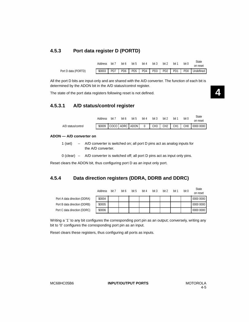
MC68HC05B6 MOTOROLA4-5
INPUT/OUTPUT PORTS
4
4.5.3 Port data register D (PORTD)
All the port D bits are input-only and are shared with the A/D converter. The function of each bit isdetermined by the ADON bit in the A/D status/control register.
The state of the port data registers following reset is not defined.
4.5.3.1 A/D status/control register
ADON — A/D converter on
1 (set) – A/D converter is switched on; all port D pins act as analog inputs forthe A/D converter.
0 (clear) – A/D converter is switched off; all port D pins act as input only pins.
Reset clears the ADON bit, thus configuring port D as an input only port.
4.5.4 Data direction registers (DDRA, DDRB and DDRC)
Writing a ‘1’ to any bit configures the corresponding port pin as an output; conversely, writing anybit to ‘0’ configures the corresponding port pin as an input.
Reset clears these registers, thus configuring all ports as inputs.
Address bit 7 bit 6 bit 5 bit 4 bit 3 bit 2 bit 1 bit 0State
on reset
Port D data (PORTD) $0003 PD7 PD6 PD5 PD4 PD3 PD2 PD1 PD0 Undefined
Address bit 7 bit 6 bit 5 bit 4 bit 3 bit 2 bit 1 bit 0State
on reset
A/D status/control $0009 COCO ADRC ADON 0 CH3 CH2 CH1 CH0 0000 0000
Address bit 7 bit 6 bit 5 bit 4 bit 3 bit 2 bit 1 bit 0State
on reset
Port A data direction (DDRA) $0004 0000 0000
Port B data direction (DDRB) $0005 0000 0000
Port C data direction (DDRC) $0006 0000 0000
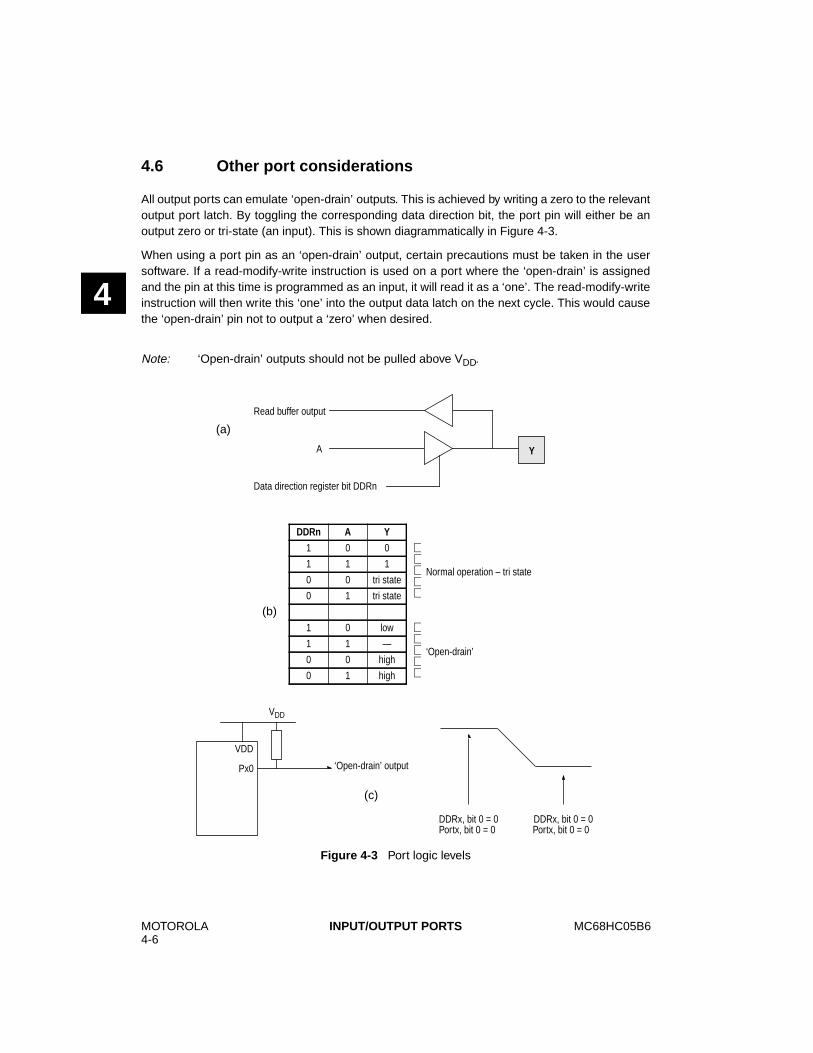
MOTOROLA4-6
MC68HC05B6INPUT/OUTPUT PORTS
4
4.6 Other port considerations
All output ports can emulate ‘open-drain’ outputs. This is achieved by writing a zero to the relevantoutput port latch. By toggling the corresponding data direction bit, the port pin will either be anoutput zero or tri-state (an input). This is shown diagrammatically in Figure 4-3.
When using a port pin as an ‘open-drain’ output, certain precautions must be taken in the usersoftware. If a read-modify-write instruction is used on a port where the ‘open-drain’ is assignedand the pin at this time is programmed as an input, it will read it as a ‘one’. The read-modify-writeinstruction will then write this ‘one’ into the output data latch on the next cycle. This would causethe ‘open-drain’ pin not to output a ‘zero’ when desired.
Note: ‘Open-drain’ outputs should not be pulled above VDD.
Figure 4-3 Port logic levels
DDRn A Y
(b)
1 0 0
Normal operation – tri state1 1 1
0 0 tri state
0 1 tri state
1 0 low
‘Open-drain’1 1 —
0 0 high
0 1 high
YA
Read buffer output
Data direction register bit DDRn
Px0
VDD
VDD
DDRx, bit 0 = 0Portx, bit 0 = 0
DDRx, bit 0 = 0Portx, bit 0 = 0
(c)
(a)
‘Open-drain’ output
MC68HC05B6 MOTOROLA5-1
PROGRAMMABLE TIMER
5
5PROGRAMMABLE TIMER
The programmable timer on the MC68HC05B6 consists of a 16-bit read-only free-running counter,with a fixed divide-by-four prescaler, plus the input capture/output compare circuitry. The timer canbe used for many purposes including measuring pulse length of two input signals and generatingtwo output signals. Pulse lengths for both input and output signals can vary from severalmicroseconds to many seconds. In addition, it works in conjunction with the pulse widthmodulation (PLM) system to execute two 8-bit D/A PLM (pulse length modulation) conversions,with a choice of two repetition rates. The timer is also capable of generating periodic interrupts orindicating passage of an arbitrary multiple of four CPU cycles. A block diagram is shown in Figure5-1, and timing diagrams are shown in Figure 5-2, Figure 5-3, Figure 5-4 and Figure 5-5.
The timer has a 16-bit architecture, hence each specific functional segment is represented by two8-bit registers (except the PLMA and PLMB which use one 8-bit register for each). These registerscontain the high and low byte of that functional segment. Accessing the low byte of a specific timerfunction allows full control of that function; however, an access of the high byte inhibits that specifictimer function until the low byte is also accessed.
The 16-bit programmable timer is monitored and controlled by a group of sixteen registers, fulldetails of which are contained in this section.
Note: A problem may arise if an interrupt occurs in the time between the high and low bytesbeing accessed. To prevent this, the I-bit in the condition code register (CCR) should beset while manipulating both the high and low byte register of a specific timer function,ensuring that an interrupt does not occur.
5.1 Counter
The key element in the programmable timer is a 16-bit, free-running counter or counter register,preceded by a prescaler that divides the internal processor clock by four. The prescaler gives thetimer a resolution of 2µs if the internal bus clock is 2 MHz. The counter is incremented during thelow portion of the internal bus clock. Software can read the counter at any time without affectingits value.
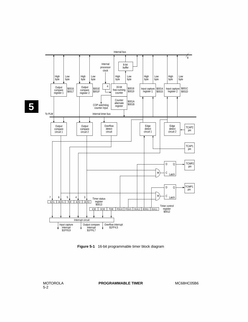
MOTOROLA5-2
MC68HC05B6PROGRAMMABLE TIMER
5
Figure 5-1 16-bit programmable timer block diagram
Internal
Internal bus
8
Outputcompareregister 1
processorclock
+
+
8-bitbuffer
4
High Low
16-bitfree-running
counter
Counteralternateregister
register 1register 2
Input capture
Internal timer bus
Overflowdetectcircuit
Edgedetect
TCAP1
TCMP2
TCMP1
Latch
D
C
Q
compareOutput
register 2Input capture
byte byteHighbyte
Lowbyte
Highbyte
Lowbyte
Highbyte
Lowbyte
Lowbyte
Highbyte
circuit 1compareOutput
circuit 2compareOutput
circuit 1
Edgedetect
circuit 2
TCAP2pin
pin
pin
pin
D
C
Q
Latch7 6 5 4 3 Timer statusregister
Timer control$0013
$0012
$0018$0019
$001A$001B
$001C$0016$0017
$0014$0015
$001E$001F $001D
To PLM
register
ICF1 OCF1 TOF ICF2 OCF2
ICIE OCIE TOIE FOLV2 OLVL2 IEDG1 OLVL1FOLV1
Interrupt circuit
Input captureinterrupt$1FF8,9
Output compareinterrupt$1FF6,7
Overflow interrupt$1FF4,5
COP watchdogcounter input
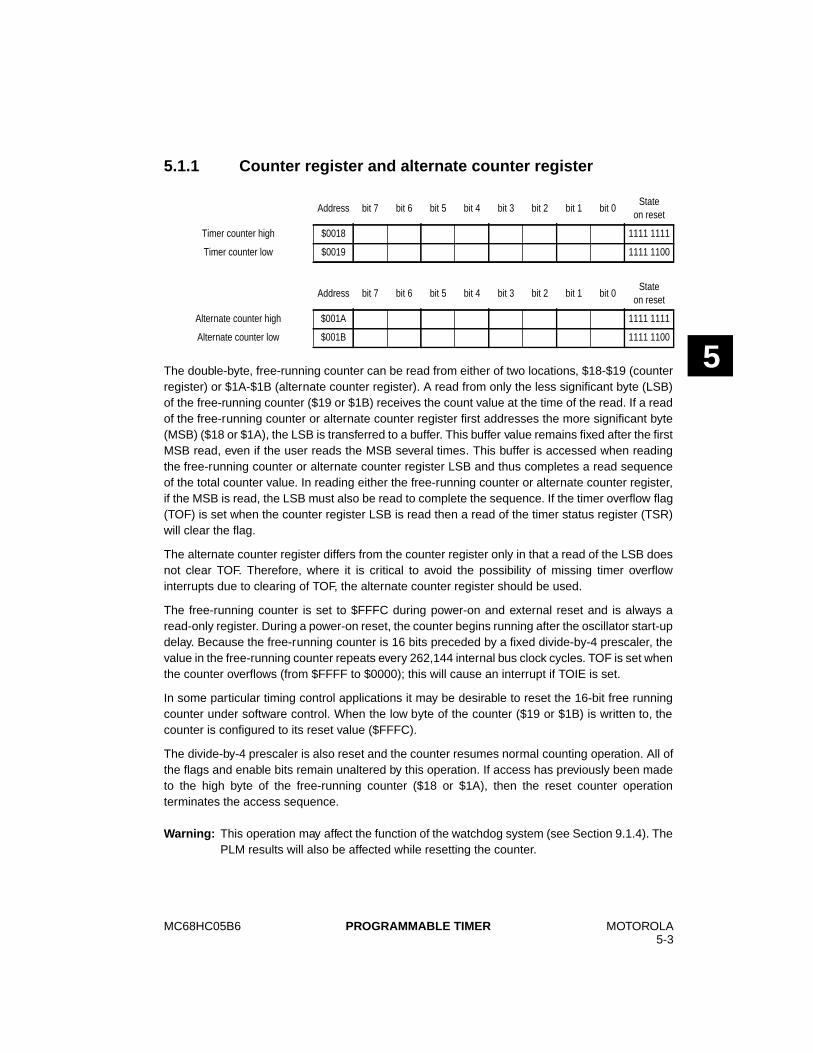
MC68HC05B6 MOTOROLA5-3
PROGRAMMABLE TIMER
5
5.1.1 Counter register and alternate counter register
The double-byte, free-running counter can be read from either of two locations, $18-$19 (counterregister) or $1A-$1B (alternate counter register). A read from only the less significant byte (LSB)of the free-running counter ($19 or $1B) receives the count value at the time of the read. If a readof the free-running counter or alternate counter register first addresses the more significant byte(MSB) ($18 or $1A), the LSB is transferred to a buffer. This buffer value remains fixed after the firstMSB read, even if the user reads the MSB several times. This buffer is accessed when readingthe free-running counter or alternate counter register LSB and thus completes a read sequenceof the total counter value. In reading either the free-running counter or alternate counter register,if the MSB is read, the LSB must also be read to complete the sequence. If the timer overflow flag(TOF) is set when the counter register LSB is read then a read of the timer status register (TSR)will clear the flag.
The alternate counter register differs from the counter register only in that a read of the LSB doesnot clear TOF. Therefore, where it is critical to avoid the possibility of missing timer overflowinterrupts due to clearing of TOF, the alternate counter register should be used.
The free-running counter is set to $FFFC during power-on and external reset and is always aread-only register. During a power-on reset, the counter begins running after the oscillator start-updelay. Because the free-running counter is 16 bits preceded by a fixed divide-by-4 prescaler, thevalue in the free-running counter repeats every 262,144 internal bus clock cycles. TOF is set whenthe counter overflows (from $FFFF to $0000); this will cause an interrupt if TOIE is set.
In some particular timing control applications it may be desirable to reset the 16-bit free runningcounter under software control. When the low byte of the counter ($19 or $1B) is written to, thecounter is configured to its reset value ($FFFC).
The divide-by-4 prescaler is also reset and the counter resumes normal counting operation. All ofthe flags and enable bits remain unaltered by this operation. If access has previously been madeto the high byte of the free-running counter ($18 or $1A), then the reset counter operationterminates the access sequence.
Warning: This operation may affect the function of the watchdog system (see Section 9.1.4). ThePLM results will also be affected while resetting the counter.
Address bit 7 bit 6 bit 5 bit 4 bit 3 bit 2 bit 1 bit 0State
on reset
Timer counter high $0018 1111 1111
Timer counter low $0019 1111 1100
Address bit 7 bit 6 bit 5 bit 4 bit 3 bit 2 bit 1 bit 0State
on reset
Alternate counter high $001A 1111 1111
Alternate counter low $001B 1111 1100
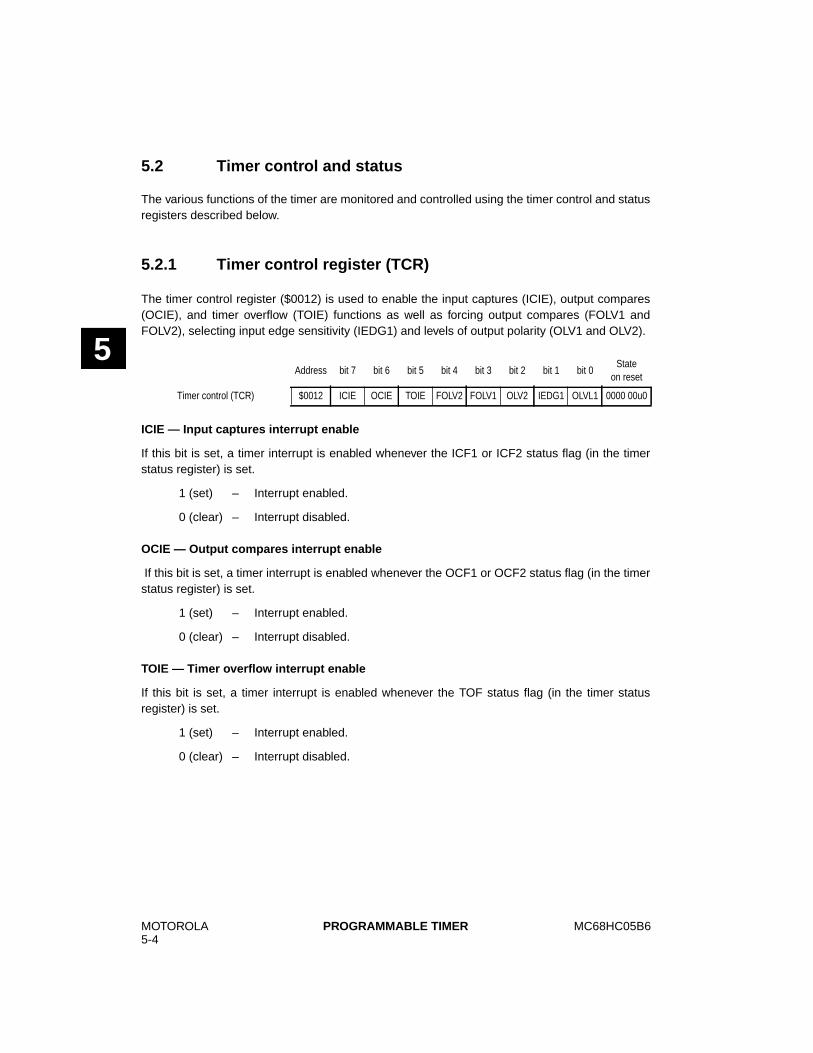
MOTOROLA5-4
MC68HC05B6PROGRAMMABLE TIMER
5
5.2 Timer control and status
The various functions of the timer are monitored and controlled using the timer control and statusregisters described below.
5.2.1 Timer control register (TCR)
The timer control register ($0012) is used to enable the input captures (ICIE), output compares(OCIE), and timer overflow (TOIE) functions as well as forcing output compares (FOLV1 andFOLV2), selecting input edge sensitivity (IEDG1) and levels of output polarity (OLV1 and OLV2).
ICIE — Input captures interrupt enable
If this bit is set, a timer interrupt is enabled whenever the ICF1 or ICF2 status flag (in the timerstatus register) is set.
1 (set) – Interrupt enabled.
0 (clear) – Interrupt disabled.
OCIE — Output compares interrupt enable
If this bit is set, a timer interrupt is enabled whenever the OCF1 or OCF2 status flag (in the timerstatus register) is set.
1 (set) – Interrupt enabled.
0 (clear) – Interrupt disabled.
TOIE — Timer overflow interrupt enable
If this bit is set, a timer interrupt is enabled whenever the TOF status flag (in the timer statusregister) is set.
1 (set) – Interrupt enabled.
0 (clear) – Interrupt disabled.
Address bit 7 bit 6 bit 5 bit 4 bit 3 bit 2 bit 1 bit 0State
on reset
Timer control (TCR) $0012 ICIE OCIE TOIE FOLV2 FOLV1 OLV2 IEDG1 OLVL1 0000 00u0
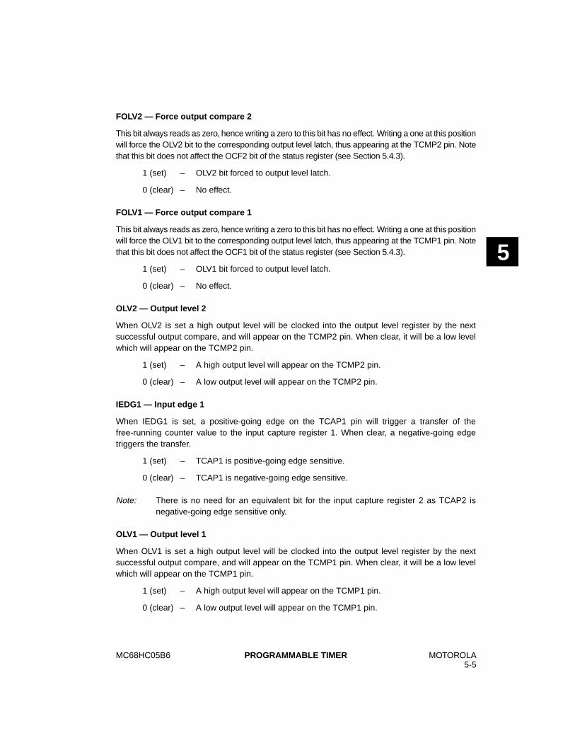
MC68HC05B6 MOTOROLA5-5
PROGRAMMABLE TIMER
5
FOLV2 — Force output compare 2
This bit always reads as zero, hence writing a zero to this bit has no effect. Writing a one at this positionwill force the OLV2 bit to the corresponding output level latch, thus appearing at the TCMP2 pin. Notethat this bit does not affect the OCF2 bit of the status register (see Section 5.4.3).
1 (set) – OLV2 bit forced to output level latch.
0 (clear) – No effect.
FOLV1 — Force output compare 1
This bit always reads as zero, hence writing a zero to this bit has no effect. Writing a one at this positionwill force the OLV1 bit to the corresponding output level latch, thus appearing at the TCMP1 pin. Notethat this bit does not affect the OCF1 bit of the status register (see Section 5.4.3).
1 (set) – OLV1 bit forced to output level latch.
0 (clear) – No effect.
OLV2 — Output level 2
When OLV2 is set a high output level will be clocked into the output level register by the nextsuccessful output compare, and will appear on the TCMP2 pin. When clear, it will be a low levelwhich will appear on the TCMP2 pin.
1 (set) – A high output level will appear on the TCMP2 pin.
0 (clear) – A low output level will appear on the TCMP2 pin.
IEDG1 — Input edge 1
When IEDG1 is set, a positive-going edge on the TCAP1 pin will trigger a transfer of thefree-running counter value to the input capture register 1. When clear, a negative-going edgetriggers the transfer.
1 (set) – TCAP1 is positive-going edge sensitive.
0 (clear) – TCAP1 is negative-going edge sensitive.
Note: There is no need for an equivalent bit for the input capture register 2 as TCAP2 isnegative-going edge sensitive only.
OLV1 — Output level 1
When OLV1 is set a high output level will be clocked into the output level register by the nextsuccessful output compare, and will appear on the TCMP1 pin. When clear, it will be a low levelwhich will appear on the TCMP1 pin.
1 (set) – A high output level will appear on the TCMP1 pin.
0 (clear) – A low output level will appear on the TCMP1 pin.
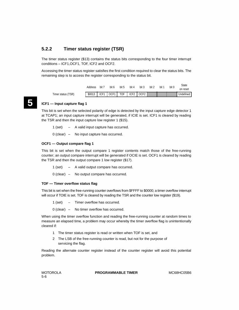
MOTOROLA5-6
MC68HC05B6PROGRAMMABLE TIMER
5
5.2.2 Timer status register (TSR)
The timer status register ($13) contains the status bits corresponding to the four timer interruptconditions – ICF1,OCF1, TOF, ICF2 and OCF2.
Accessing the timer status register satisfies the first condition required to clear the status bits. Theremaining step is to access the register corresponding to the status bit.
ICF1 — Input capture flag 1
This bit is set when the selected polarity of edge is detected by the input capture edge detector 1at TCAP1; an input capture interrupt will be generated, if ICIE is set. ICF1 is cleared by readingthe TSR and then the input capture low register 1 ($15).
1 (set) – A valid input capture has occurred.
0 (clear) – No input capture has occurred.
OCF1 — Output compare flag 1
This bit is set when the output compare 1 register contents match those of the free-runningcounter; an output compare interrupt will be generated if OCIE is set. OCF1 is cleared by readingthe TSR and then the output compare 1 low register ($17).
1 (set) – A valid output compare has occurred.
0 (clear) – No output compare has occurred.
TOF — Timer overflow status flag
This bit is set when the free-running counter overflows from $FFFF to $0000; a timer overflow interruptwill occur if TOIE is set. TOF is cleared by reading the TSR and the counter low register ($19).
1 (set) – Timer overflow has occurred.
0 (clear) – No timer overflow has occurred.
When using the timer overflow function and reading the free-running counter at random times tomeasure an elapsed time, a problem may occur whereby the timer overflow flag is unintentionallycleared if:
1 The timer status register is read or written when TOF is set, and
2 The LSB of the free-running counter is read, but not for the purpose ofservicing the flag.
Reading the alternate counter register instead of the counter register will avoid this potentialproblem.
Address bit 7 bit 6 bit 5 bit 4 bit 3 bit 2 bit 1 bit 0State
on reset
Timer status (TSR) $0013 ICF1 OCF1 TOF ICF2 OCF2 Undefined
MC68HC05B6 MOTOROLA5-7
PROGRAMMABLE TIMER
5
ICF2 — Input capture flag 2
This bit is set when a negative edge is detected by the input capture edge detector 2 at TCAP2;an input capture interrupt will be generated if ICIE is set. ICF2 is cleared by reading the TSR andthen the input capture low register 2 ($1D).
1 (set) – A valid (negative) input capture has occurred.
0 (clear) – No input capture has occurred.
OCF2 — Output compare flag 2
This bit is set when the output compare 2 register contents match those of the free-runningcounter; an output compare interrupt will be generated if OCIE is set. OCF2 is cleared by readingthe TSR and then the output compare 2 low register ($1F).
1 (set) – A valid output compare has occurred.
0 (clear) – No output compare has occurred.
5.3 Input capture
‘Input capture’ is a technique whereby an external signal is used to trigger a read of the freerunning counter. In this way it is possible to relate the timing of an external signal to the internalcounter value, and hence to elapsed time.
There are two input capture registers: input capture register 1 (ICR1) and input capture register 2 (ICR2).
The same input capture interrupt enable bit (ICIE) is used for the two input captures.
5.3.1 Input capture register 1 (ICR1)
The two 8-bit registers that make up the 16-bit input capture register 1 are read-only, and are usedto latch the value of the free-running counter after the input capture edge detector circuit 1 sensesa valid transition at TCAP1. The level transition that triggers the counter transfer is defined by theinput edge bit (IEDG1). When an input capture 1 occurs, the corresponding flag ICF1 in TSR isset. An interrupt can also accompany an input capture 1 provided the ICIE bit in TCR is set. The8 most significant bits are stored in the input capture high 1 register at $14, the 8 least significantbits in the input capture low 1 register at $15.
Address bit 7 bit 6 bit 5 bit 4 bit 3 bit 2 bit 1 bit 0State
on reset
Input capture high 1 $0014 Undefined
Input capture low 1 $0015 Undefined
MOTOROLA5-8
MC68HC05B6PROGRAMMABLE TIMER
5
The result obtained from an input capture will be one greater than the value of the free-runningcounter on the rising edge of the internal bus clock preceding the external transition. This delay isrequired for internal synchronization. Resolution is one count of the free-running counter, which isfour internal bus clock cycles. The free-running counter contents are transferred to the inputcapture register 1 on each valid signal transition whether the input capture 1 flag (ICF1) is set orclear. The input capture register 1 always contains the free-running counter value thatcorresponds to the most recent input capture 1. After a read of the input capture 1 register MSB($14), the counter transfer is inhibited until the LSB ($15) is also read. This characteristic causesthe time used in the input capture software routine and its interaction with the main program todetermine the minimum pulse period. A read of the input capture 1 register LSB ($15) does notinhibit the free-running counter transfer since the two actions occur on opposite edges of theinternal bus clock.
Reset does not affect the contents of the input capture 1 register, except when exiting STOP mode(see Section 5.6).
5.3.2 Input capture register 2 (ICR2)
The two 8-bit registers that make up the 16-bit input capture register 2 are read-only, and are usedto latch the value of the free-running counter after the input capture edge detector circuit 2 sensesa negative transition at pin TCAP2. When an input capture 2 occurs, the corresponding flag ICF2in TSR is set. An interrupt can also accompany an input capture 2 provided the ICIE bit in TCR isset.The 8 most significant bits are stored in the input capture 2 high register at $1C, the 8 leastsignificant bits in the input capture 2 low register at $1D.
The result obtained from an input capture will be one greater than the value of the free-runningcounter on the rising edge of the internal bus clock preceding the external transition. This delay isrequired for internal synchronization. Resolution is one count of the free-running counter, which isfour internal bus clock cycles. The free-running counter contents are transferred to the inputcapture register 2 on each negative signal transition whether the input capture 2 flag (IC2F) is setor clear. The input capture register 2 always contains the free-running counter value thatcorresponds to the most recent input capture 2. After a read of the input capture register 2 MSB($1C), the counter transfer is inhibited until the LSB ($1D) is also read. This characteristic causesthe time used in the input capture software routine and its interaction with the main program todetermine the minimum pulse period. A read of the input capture register 2 LSB ($1C) does notinhibit the free-running counter transfer since the two actions occur on opposite edges of theinternal bus clock.
Reset does not affect the contents of the input capture 2 register, except when exiting STOP mode(see Section 5.6).
Address bit 7 bit 6 bit 5 bit 4 bit 3 bit 2 bit 1 bit 0State
on reset
Input capture high 2 $001C Undefined
Input capture low 2 $001D Undefined
MC68HC05B6 MOTOROLA5-9
PROGRAMMABLE TIMER
5
5.4 Output compare
‘Output compare’ is a technique which may be used, for example, to generate an output waveform,or to signal when a specific time period has elapsed, by presetting the output compare register tothe appropriate value.
There are two output compare registers: output compare register 1 (OCR1) and output compareregister 2 (OCR2).
Note: The same output compare interrupt enable bit (OCIE) is used for the two outputcompares.
5.4.1 Output compare register 1 (OCR1)
The 16-bit output compare register 1 is made up of two 8-bit registers at locations $16 (MSB) and$17 (LSB). The contents of the output compare register 1 are compared with the contents of thefree-running counter continually and, if a match is found, the corresponding output compare flag(OCF1) in the timer status register is set and the output level (OLVL1) is transferred to pin TCMP1.The output compare register 1 values and the output level bit should be changed after eachsuccessful comparison to establish a new elapsed timeout. An interrupt can also accompany asuccessful output compare provided the corresponding interrupt enable bit (OCIE) is set. (Thefree-running counter is updated every four internal bus clock cycles.)
After a processor write cycle to the output compare register 1 containing the MSB ($16), the outputcompare function is inhibited until the LSB ($17) is also written. The user must write both bytes(locations) if the MSB is written first. A write made only to the LSB ($17) will not inhibit the compare1 function. The processor can write to either byte of the output compare register 1 without affectingthe other byte. The output level (OLVL1) bit is clocked to the output level register and hence to theTCMP1 pin whether the output compare flag 1 (OCF1) is set or clear. The minimum time requiredto update the output compare register 1 is a function of the program rather than the internalhardware. Because the output compare flag 1 and the output compare register 1 are not definedat power on, and not affected by reset, care must be taken when initializing output comparefunctions with software. The following procedure is recommended:
– Write to output compare high 1 to inhibit further compares;
– Read the timer status register to clear OCF1 (if set);
– Write to output compare low 1 to enable the output compare 1 function.
Address bit 7 bit 6 bit 5 bit 4 bit 3 bit 2 bit 1 bit 0State
on reset
Output compare high 1 $0016 Undefined
Output compare low 1 $0017 Undefined
MOTOROLA5-10
MC68HC05B6PROGRAMMABLE TIMER
5
The purpose of this procedure is to prevent the OCF1 bit from being set between the time it is readand the write to the corresponding output compare register.
All bits of the output compare register are readable and writable and are not altered by the timerhardware or reset. If the compare function is not needed, the two bytes of the output compareregister can be used as storage locations.
5.4.2 Output compare register 2 (OCR2)
The 16-bit output compare register 2 is made up of two 8-bit registers at locations $1E (MSB) and$1F (LSB). The contents of the output compare register 2 are compared with the contents of thefree-running counter continually and, if a match is found, the corresponding output compare flag(OCF2) in the timer status register is set and the output level (OLVL2) is transferred to pin TCMP2.The output compare register 2 values and the output level bit should be changed after eachsuccessful comparison to establish a new elapsed timeout. An interrupt can also accompany asuccessful output compare provided the corresponding interrupt enable bit (OCIE) is set. (Thefree-running counter is updated every four internal bus clock cycles.)
After a processor write cycle to the output compare register 2 containing the MSB ($1E), theoutput compare function is inhibited until the LSB ($1F) is also written. The user must write bothbytes (locations) if the MSB is written first. A write made only to the LSB ($1F) will not inhibit thecompare 2 function. The processor can write to either byte of the output compare register 2without affecting the other byte. The output level (OLVL2) bit is clocked to the output level registerand hence to the TCMP2 pin whether the output compare flag 2 (OCF2) is set or clear. Theminimum time required to update the output compare register 2 is a function of the program ratherthan the internal hardware. Because the output compare flag 2 and the output compare register2 are not defined at power on, and not affected by reset, care must be taken when initializingoutput compare functions with software. The following procedure is recommended:
– Write to output compare high 2 to inhibit further compares;
– Read the timer status register to clear OCF2 (if set);
– Write to output compare low 2 to enable the output compare 2 function.
Address bit 7 bit 6 bit 5 bit 4 bit 3 bit 2 bit 1 bit 0State
on reset
Output compare high 2 $001E Undefined
Output compare low 2 $001F Undefined
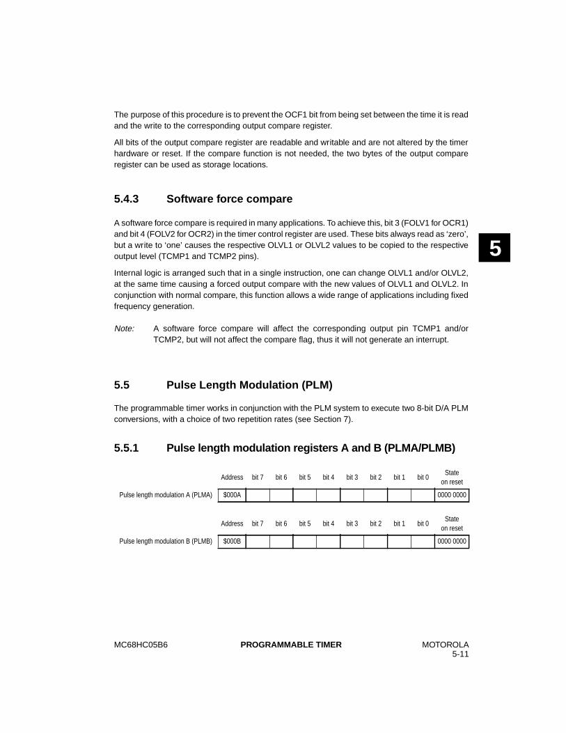
MC68HC05B6 MOTOROLA5-11
PROGRAMMABLE TIMER
5
The purpose of this procedure is to prevent the OCF1 bit from being set between the time it is readand the write to the corresponding output compare register.
All bits of the output compare register are readable and writable and are not altered by the timerhardware or reset. If the compare function is not needed, the two bytes of the output compareregister can be used as storage locations.
5.4.3 Software force compare
A software force compare is required in many applications. To achieve this, bit 3 (FOLV1 for OCR1)and bit 4 (FOLV2 for OCR2) in the timer control register are used. These bits always read as ‘zero’,but a write to ‘one’ causes the respective OLVL1 or OLVL2 values to be copied to the respectiveoutput level (TCMP1 and TCMP2 pins).
Internal logic is arranged such that in a single instruction, one can change OLVL1 and/or OLVL2,at the same time causing a forced output compare with the new values of OLVL1 and OLVL2. Inconjunction with normal compare, this function allows a wide range of applications including fixedfrequency generation.
Note: A software force compare will affect the corresponding output pin TCMP1 and/orTCMP2, but will not affect the compare flag, thus it will not generate an interrupt.
5.5 Pulse Length Modulation (PLM)
The programmable timer works in conjunction with the PLM system to execute two 8-bit D/A PLMconversions, with a choice of two repetition rates (see Section 7).
5.5.1 Pulse length modulation register s A and B (PLMA/PLMB)
Address bit 7 bit 6 bit 5 bit 4 bit 3 bit 2 bit 1 bit 0State
on reset
Pulse length modulation A (PLMA) $000A 0000 0000
Address bit 7 bit 6 bit 5 bit 4 bit 3 bit 2 bit 1 bit 0State
on reset
Pulse length modulation B (PLMB) $000B 0000 0000
MOTOROLA5-12
MC68HC05B6PROGRAMMABLE TIMER
5
5.6 Timer during STOP mode
When the MCU enters STOP mode, the timer counter stops counting and remains at thatparticular count value until STOP mode is exited by an interrupt. If STOP mode is exited bypower-on or external reset, the counter is forced to $FFFC but if it is exited by external interrupt(IRQ) then the counter resumes from its stopped value.
Another feature of the programmable timer is that if at least one valid input capture edge occursat one of the TCAP pins while in STOP mode, the corresponding input capture detect circuitry isarmed. This action does not wake the MCU or set any timer flags, but when the MCU doeswake-up there will be an active input capture flag (and data) from that first valid edge whichoccurred during STOP mode.
If STOP mode is exited by an external reset then no such input capture flag or data action takesplace even if there was a valid input capture edge (at one of the TCAP pins) during STOP mode.
5.7 Timer during WAIT mode
The timer system is not affected by WAIT mode and continues normal operation. Any valid timerinterrupt will wake-up the system.
5.8 Timer state diagrams
The relationships between the internal clock signals, the counter contents and the status of theflag bits are shown in the following figures. It should be noted that the signals labelled ‘internal’(processor clock, timer clocks and reset) are not available to the user.
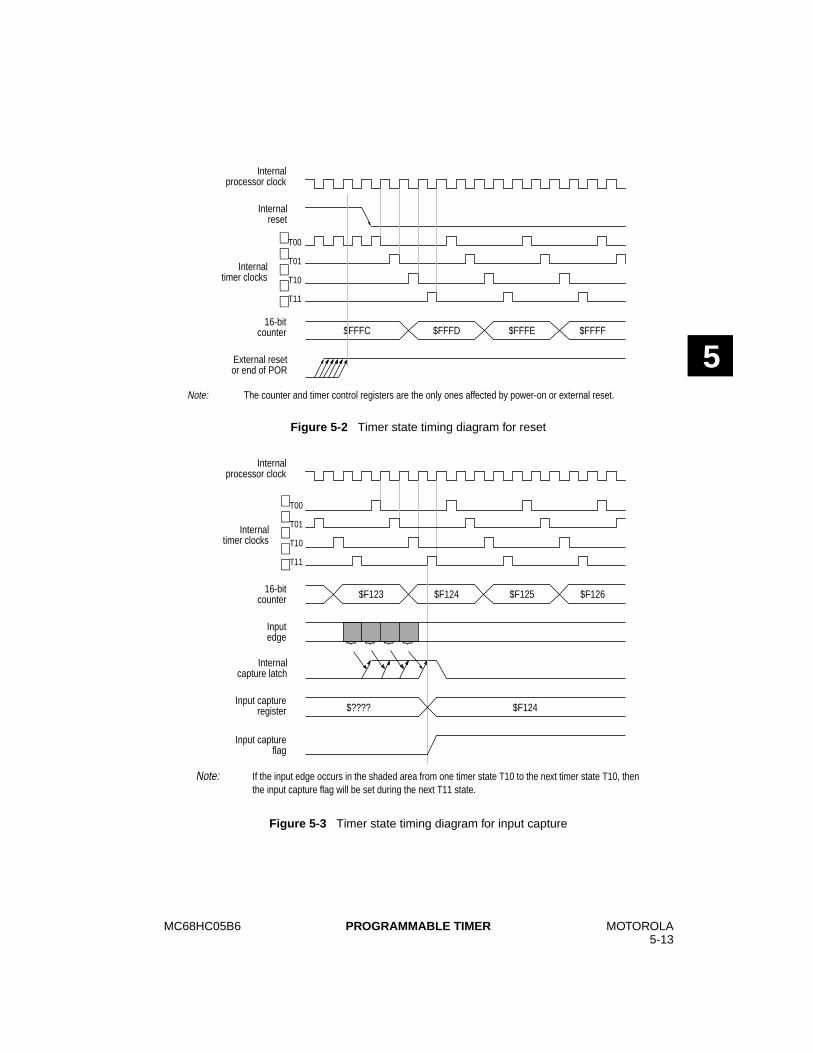
MC68HC05B6 MOTOROLA5-13
PROGRAMMABLE TIMER
5
Figure 5-2 Timer state timing diagram for reset
Figure 5-3 Timer state timing diagram for input capture
Internalprocessor clock
Internalreset
16-bitcounter
External resetor end of POR
Internaltimer clocks
$FFFC $FFFD $FFFE $FFFF
Note: The counter and timer control registers are the only ones affected by power-on or external reset.
T00
T01
T11
T10
Internalprocessor clock
16-bitcounter $F123 $F124 $F125 $F126
Internaltimer clocks
T00
T01
T11
T10
Internalcapture latch
$F124$????Input capture
register
Input captureflag
Inputedge } } } }
Note: If the input edge occurs in the shaded area from one timer state T10 to the next timer state T10, thenthe input capture flag will be set during the next T11 state.
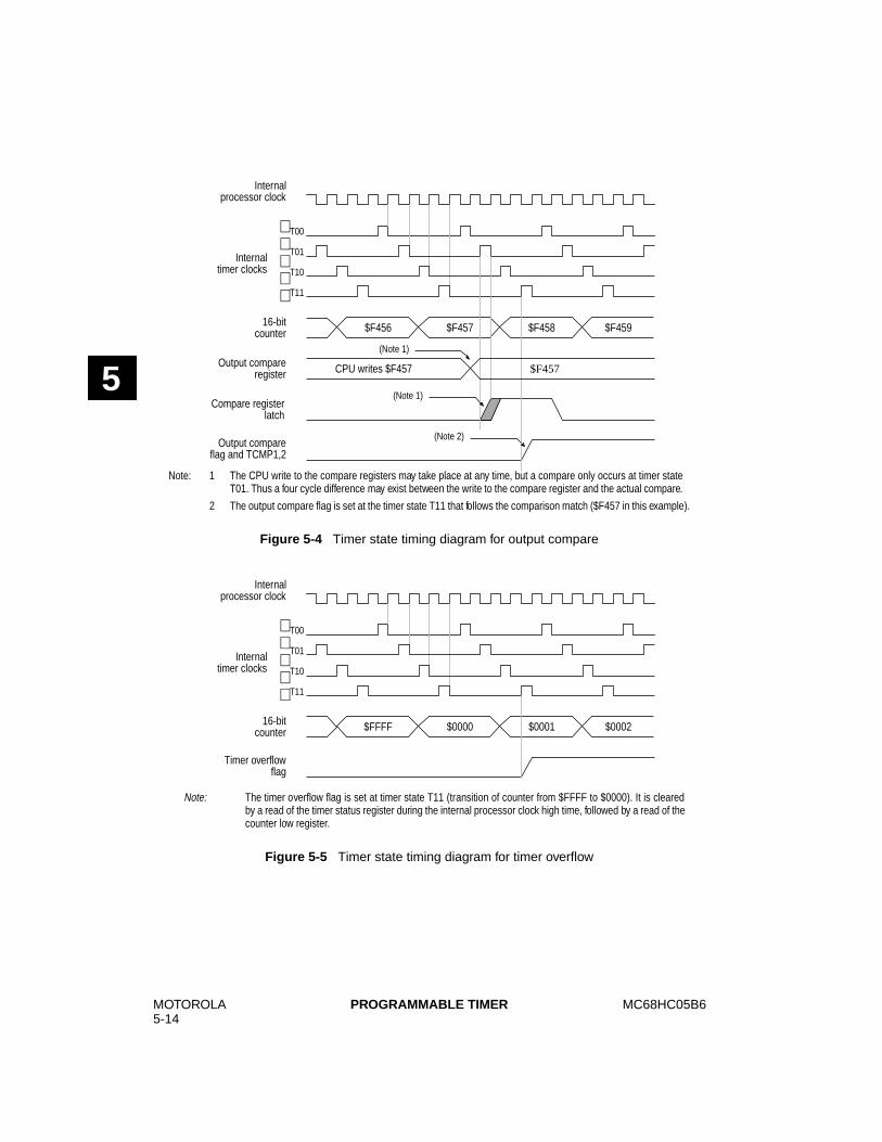
MOTOROLA5-14
MC68HC05B6PROGRAMMABLE TIMER
5
Figure 5-4 Timer state timing diagram for output compare
Figure 5-5 Timer state timing diagram for timer overflow
Internalprocessor clock
16-bitcounter $F456 $F457 $F458 $F459
Internaltimer clocks
T00
T01
T11
T10
$F457CPU writes $F457
Output compareflag and TCMP1,2
Note: 1 The CPU write to the compare registers may take place at any time, but a compare only occurs at timer stateT01. Thus a four cycle difference may exist between the write to the compare register and the actual compare.
2 The output compare flag is set at the timer state T11 that follows the comparison match ($F457 in this example).
Output compareregister
Compare registerlatch
(Note 2)
(Note 1)
(Note 1)
Internalprocessor clock
16-bitcounter $FFFF $0000 $0001 $0002
Internaltimer clocks
T00
T01
T11
T10
Note: The timer overflow flag is set at timer state T11 (transition of counter from $FFFF to $0000). It is clearedby a read of the timer status register during the internal processor clock high time, followed by a read of thecounter low register.
Timer overflowflag
MC68HC05B6 MOTOROLA6-1
SERIAL COMMUNICATIONS INTERFACE
6
6SERIAL COMMUNICATIONS INTERFACE
A full-duplex asynchronous serial communications interface (SCI) is provided with a standardnon-return-to-zero (NRZ) format and a variety of baud rates. The SCI transmitter and receiver arefunctionally independent and have their own baud rate generator; however they share a commonbaud rate prescaler and data format.
The serial data format is standard mark/space (NRZ) and provides one start bit, eight or nine databits, and one stop bit.
The SCLK pin is the output of the transmitter clock. It outputs the transmitter data clock forsynchronous transmission (no clocks on start bit and stop bit, and a software option to send clockon last data bit). This allows control of peripherals containing shift registers (e.g. LCD drivers).Phase and polarity of these clocks are software programmable.
Any SCI bidirectional communication requires a two-wire system: receive data in (RDI) andtransmit data out (TDO).
‘Baud’ and ‘bit rate’ are used synonymously in the following description.
6.1 SCI two-wire system features
• Standard NRZ (mark/space) format
• Advanced error detection method with noise detection for noise duration of up to 1/16th bit time
• Full-duplex operation (simultaneous transmit and receive)
• 32 software selectable baud rates
• Different baud rates for transmit and receive; for each transmit baud rate, 8 possible receivebaud rates
• Software selectable word length (eight or nine bits)
• Separate transmitter and receiver enable bits
• Capable of being interrupt driven
• Transmitter clocks available without altering the regular transmitter or receiver functions
• Four separate enable bits for interrupt control
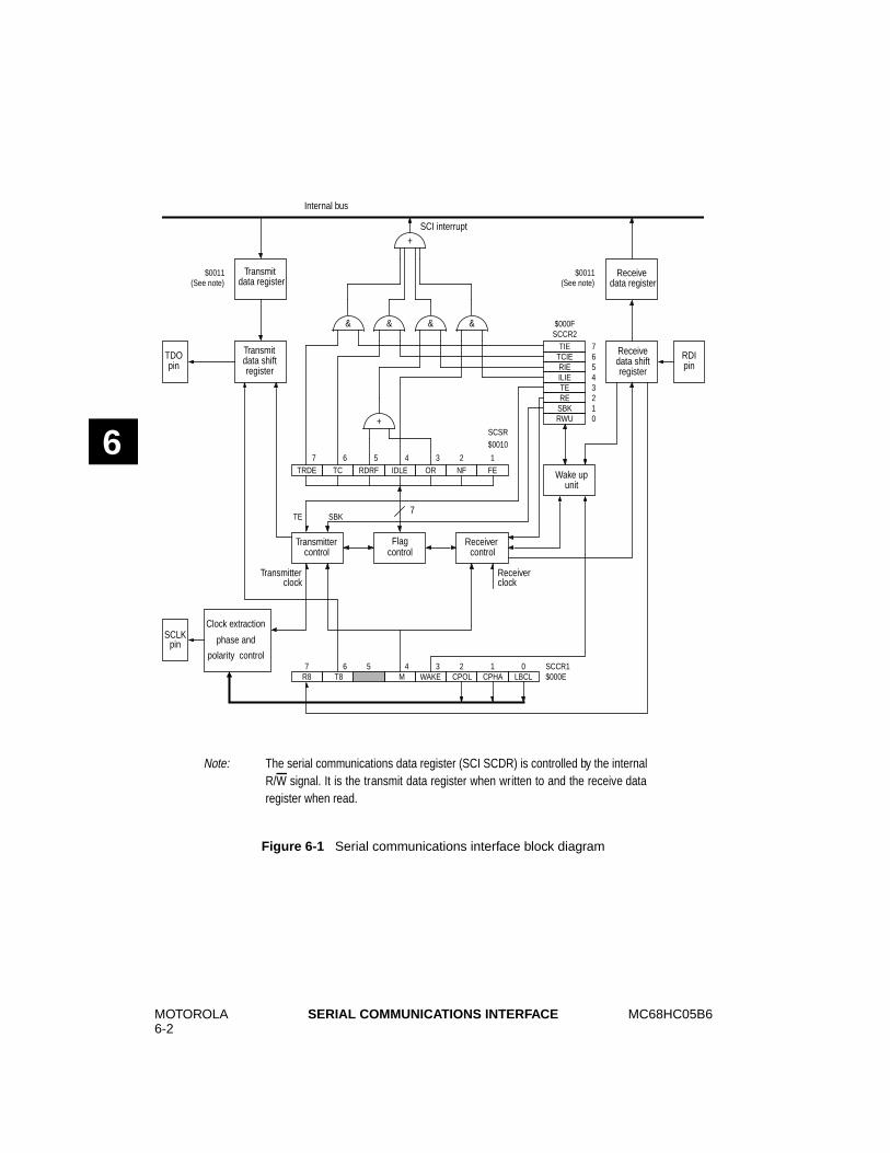
MOTOROLA6-2
MC68HC05B6SERIAL COMMUNICATIONS INTERFACE
6
Figure 6-1 Serial communications interface block diagram
& & & &
+
+
Internal bus
SCI interrupt
Transmit Receive
TDOpin
RDI
Transmittercontrol
Receivercontrol
clock
Clock extraction
phase and
polarity control
pin
Receiverclock
Transmitter
Flagcontrol
data register data register
TIETCIERIEILIETERE
SBKRWU
76
5
4
3
210
$000FSCCR2
SCSR$0010
SCCR1$000E
TRDE TC RDRF IDLE OR NF FE
TE SBK
$0011(See note) (See note)
R8 T8 M WAKE CPOL CPHA LBCL012
4
3
6
5
7
7 6 5 2
34
1
SCLKpin
Wake upunit
Receivedata shiftregister
Transmitdata shiftregister
$0011
Note: The serial communications data register (SCI SCDR) is controlled by the internalR/W signal. It is the transmit data register when written to and the receive dataregister when read.
7
MC68HC05B6 MOTOROLA6-3
SERIAL COMMUNICATIONS INTERFACE
6
6.2 SCI receiver features
• Receiver wake-up function (idle line or address bit)
• Idle line detection
• Framing error detection
• Noise detection
• Overrun detection
• Receiver data register full flag
6.3 SCI transmitter features
• Transmit data register empty flag
• Transmit complete flag
• Send break
6.4 Functional description
A block diagram of the SCI is shown in Figure 6-1. Option bits in serial control register1 (SCCR1)select the ‘wake-up’ method (WAKE bit) and data word length (M-bit) of the SCI. SCCR2 providescontrol bits that individually enable the transmitter and receiver, enable system interrupts andprovide the wake-up enable bit (RWU) and the send break code bit (SBK). Control bits in the baudrate register (BAUD) allow the user to select one of 32 different baud rates for the transmitter andreceiver (see Section 6.11.5).
Data transmission is initiated by writing to the serial communications data register (SCDR).Provided the transmitter is enabled, data stored in the SCDR is transferred to the transmit datashift register. This transfer of data sets the transmit data register empty flag (TDRE) in the SCIstatus register (SCSR) and generates an interrupt (if transmitter interrupts are enabled). Thetransfer of data to the transmit data shift register is synchronized with the bit rate clock (see Figure6-2). All data is transmitted least significant bit first. Upon completion of data transmission, thetransmission complete flag (TC) in the SCSR is set (provided no pending data, preamble or breakis to be sent) and an interrupt is generated (if the transmit complete interrupt is enabled). If thetransmitter is disabled, and the data, preamble or break (in the transmit data shift register) hasbeen sent, the TC bit will also be set. This will also generate an interrupt if the transmissioncomplete interrupt enable bit (TCIE) is set. If the transmitter is disabled during a transmission, thecharacter being transmitted will be completed before the transmitter gives up control of theTDO pin.
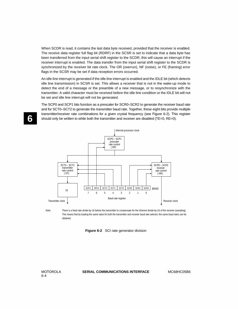
MOTOROLA6-4
MC68HC05B6SERIAL COMMUNICATIONS INTERFACE
6
When SCDR is read, it contains the last data byte received, provided that the receiver is enabled.The receive data register full flag bit (RDRF) in the SCSR is set to indicate that a data byte hasbeen transferred from the input serial shift register to the SCDR; this will cause an interrupt if thereceiver interrupt is enabled. The data transfer from the input serial shift register to the SCDR issynchronized by the receiver bit rate clock. The OR (overrun), NF (noise), or FE (framing) errorflags in the SCSR may be set if data reception errors occurred.
An idle line interrupt is generated if the idle line interrupt is enabled and the IDLE bit (which detectsidle line transmission) in SCSR is set. This allows a receiver that is not in the wake-up mode todetect the end of a message or the preamble of a new message, or to resynchronize with thetransmitter. A valid character must be received before the idle line condition or the IDLE bit will notbe set and idle line interrupt will not be generated.
The SCP0 and SCP1 bits function as a prescaler for SCR0–SCR2 to generate the receiver baud rateand for SCT0–SCT2 to generate the transmitter baud rate. Together, these eight bits provide multipletransmitter/receiver rate combinations for a given crystal frequency (see Figure 6-2). This registershould only be written to while both the transmitter and receiver are disabled (TE=0, RE=0).
Figure 6-2 SCI rate generator division
SCP1 SPC0 SCT2 SCT1 SCT0 SCR2 SCR1 SCR0
Internal processor clock
SCP0 – SCP1prescaler
rate control( NP)
SCR0 – SCR2receiver
( NR)
SCT0 – SCT2transmitterrate control
( NT)
16
Transmitter clock Receiver clock
rate control
7 6 5 4 3 2 1 0
$000D
Baud rate register
Note: There is a fixed rate divide-by-16 before the transmitter to compensate for the inherent divide-by-16 of the receiver (sampling).This means that by loading the same value for both the transmitter and receiver baud rate selector, the same baud rates can beobtained.
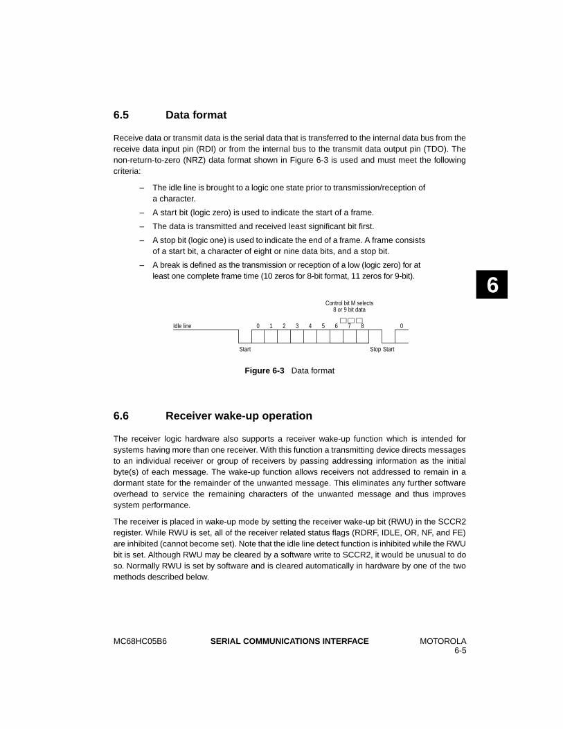
MC68HC05B6 MOTOROLA6-5
SERIAL COMMUNICATIONS INTERFACE
6
6.5 Data format
Receive data or transmit data is the serial data that is transferred to the internal data bus from thereceive data input pin (RDI) or from the internal bus to the transmit data output pin (TDO). Thenon-return-to-zero (NRZ) data format shown in Figure 6-3 is used and must meet the followingcriteria:
– The idle line is brought to a logic one state prior to transmission/reception ofa character.
– A start bit (logic zero) is used to indicate the start of a frame.
– The data is transmitted and received least significant bit first.
– A stop bit (logic one) is used to indicate the end of a frame. A frame consistsof a start bit, a character of eight or nine data bits, and a stop bit.
– A break is defined as the transmission or reception of a low (logic zero) for atleast one complete frame time (10 zeros for 8-bit format, 11 zeros for 9-bit).
6.6 Receiver wake-up operation
The receiver logic hardware also supports a receiver wake-up function which is intended forsystems having more than one receiver. With this function a transmitting device directs messagesto an individual receiver or group of receivers by passing addressing information as the initialbyte(s) of each message. The wake-up function allows receivers not addressed to remain in adormant state for the remainder of the unwanted message. This eliminates any further softwareoverhead to service the remaining characters of the unwanted message and thus improvessystem performance.
The receiver is placed in wake-up mode by setting the receiver wake-up bit (RWU) in the SCCR2register. While RWU is set, all of the receiver related status flags (RDRF, IDLE, OR, NF, and FE)are inhibited (cannot become set). Note that the idle line detect function is inhibited while the RWUbit is set. Although RWU may be cleared by a software write to SCCR2, it would be unusual to doso. Normally RWU is set by software and is cleared automatically in hardware by one of the twomethods described below.
Figure 6-3 Data format
StartStop
Control bit M selects8 or 9 bit data
Start
Idle line 0 1 2 3 4 5 6 7 8
0
MOTOROLA6-6
MC68HC05B6SERIAL COMMUNICATIONS INTERFACE
6
6.6.1 Idle line wake-up
In idle line wake-up mode, a dormant receiver wakes up as soon as the RDI line becomes idle.Idle is defined as a continuous logic high level on the RDI line for ten (or eleven) full bit times.Systems using this type of wake-up must provide at least one character time of idle betweenmessages to wake up sleeping receivers, but must not allow any idle time between characterswithin a message.
6.6.2 Address mark wake-up
In address mark wake-up, the most significant bit (MSB) in a character is used to indicate whetherit is an address (1) or data (0) character. Sleeping receivers will wake up whenever an addresscharacter is received. Systems using this method for wake-up would set the MSB of the firstcharacter of each message and leave it clear for all other characters in the message. Idle periodsmay be present within messages and no idle time is required between messages for this wake-upmethod.
6.7 Receive data in (RDI)
Receive data is the serial data that is applied through the input line and the SCI to the internal bus.The receiver circuitry clocks the input at a rate equal to 16 times the baud rate. This time is referredto as the RT rate in Figure 6-4 and as the receiver clock in Figure 6-2.
The receiver clock generator is controlled by the baud rate register, as shown in Figure 6-1 andFigure 6-2; however, the SCI is synchronized by the start bit, independent of the transmitter.
Once a valid start bit is detected, the start bit, each data bit and the stop bit are sampled threetimes at RT intervals 8 RT, 9 RT and 10 RT (1 RT is the position where the bit is expected to start),as shown in Figure 6-5. The value of the bit is determined by voting logic which takes the value ofthe majority of the samples. A noise flag is set when all three samples on a valid start bit or databit or the stop bit do not agree.
6.8 Start bit detection
When the input (idle) line is detected low, it is tested for three more sample times (referred to asthe start edge verification samples in Figure 6-4). If at least two of these three verification samplesdetect a logic zero, a valid start bit has been detected, otherwise the line is assumed to be idle. Anoise flag is set if one of the three verification samples detect a logic one, thus a valid start bitcould be assumed with a set noise flag present.
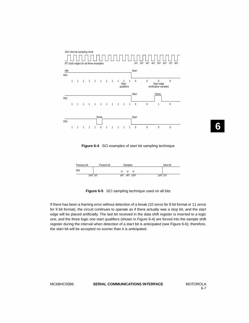
MC68HC05B6 MOTOROLA6-7
SERIAL COMMUNICATIONS INTERFACE
6
If there has been a framing error without detection of a break (10 zeros for 8 bit format or 11 zerosfor 9 bit format), the circuit continues to operate as if there actually was a stop bit, and the startedge will be placed artificially. The last bit received in the data shift register is inverted to a logicone, and the three logic one start qualifiers (shown in Figure 6-4) are forced into the sample shiftregister during the interval when detection of a start bit is anticipated (see Figure 6-6); therefore,the start bit will be accepted no sooner than it is anticipated.
Figure 6-4 SCI examples of start bit sampling technique
Figure 6-5 SCI sampling technique used on all bits
1 1 1 11 1 1111 1 0 0 0 0
1RT 2RT 3RT 5RT 7RT4RT 6RT 8RT
Start
qualifiers
Idle
Start edgeverification samples
16X internal sampling clock
RT clock edges for all three examples
Noise
Start
1 1 1 11 1 1110 1 0 0 0 0
1 1 1 11 1 1111 1 0 0 1 0
Start
Start
Noise
RDI
RDI
RDI
<< <
SamplesPresent bit Next bitPrevious bit
16RT 1RT 8RT 9RT 10RT 16RT 1RT
RDI
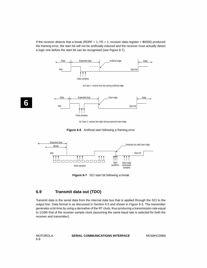
MOTOROLA6-8
MC68HC05B6SERIAL COMMUNICATIONS INTERFACE
6
If the receiver detects that a break (RDRF = 1, FE = 1, receiver data register = $0000) producedthe framing error, the start bit will not be artificially induced and the receiver must actually detecta logic one before the start bit can be recognised (see Figure 6-7).
6.9 Transmit data out (TDO)
Transmit data is the serial data from the internal data bus that is applied through the SCI to theoutput line. Data format is as discussed in Section 6.5 and shown in Figure 6-3. The transmittergenerates a bit time by using a derivative of the RT clock, thus producing a transmission rate equalto 1/16th that of the receiver sample clock (assuming the same baud rate is selected for both thereceiver and transmitter).
Figure 6-6 Artificial start following a framing error
Figure 6-7 SCI start bit following a break
Data Expected stop
Data samples
Artificial edge
Start bit
Data
RDI
Data Expected stop
Data samples
Start edge
Start bit
Data
RDI
a) Case 1: receive line low during artificial edge
b) Case 2: receive line high during expected start edge
Expected stop
Data samples
Detected as valid start edge
Start bitRDI
Break
Startqualifiers
Start edgeverificationsamples
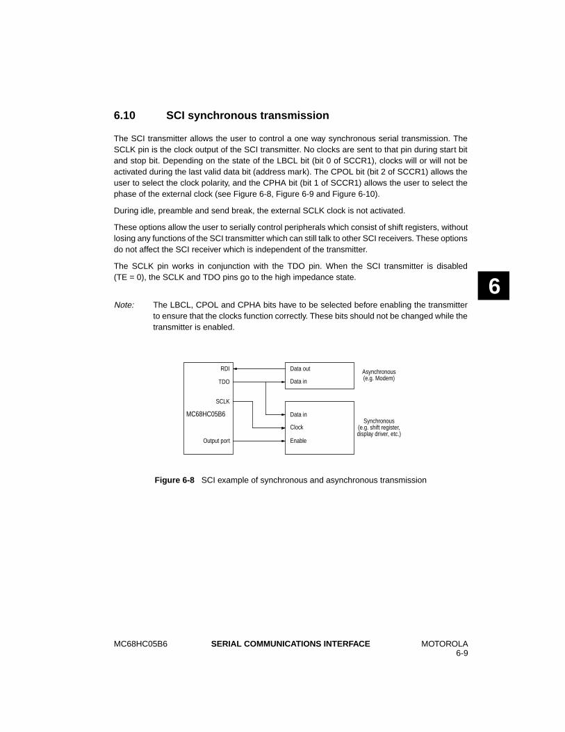
MC68HC05B6 MOTOROLA6-9
SERIAL COMMUNICATIONS INTERFACE
6
6.10 SCI synchronous transmission
The SCI transmitter allows the user to control a one way synchronous serial transmission. TheSCLK pin is the clock output of the SCI transmitter. No clocks are sent to that pin during start bitand stop bit. Depending on the state of the LBCL bit (bit 0 of SCCR1), clocks will or will not beactivated during the last valid data bit (address mark). The CPOL bit (bit 2 of SCCR1) allows theuser to select the clock polarity, and the CPHA bit (bit 1 of SCCR1) allows the user to select thephase of the external clock (see Figure 6-8, Figure 6-9 and Figure 6-10).
During idle, preamble and send break, the external SCLK clock is not activated.
These options allow the user to serially control peripherals which consist of shift registers, withoutlosing any functions of the SCI transmitter which can still talk to other SCI receivers. These optionsdo not affect the SCI receiver which is independent of the transmitter.
The SCLK pin works in conjunction with the TDO pin. When the SCI transmitter is disabled(TE = 0), the SCLK and TDO pins go to the high impedance state.
Note: The LBCL, CPOL and CPHA bits have to be selected before enabling the transmitterto ensure that the clocks function correctly. These bits should not be changed while thetransmitter is enabled.
Figure 6-8 SCI example of synchronous and asynchronous transmission
RDI
TDO
SCLK
Output port
Data out
Data in
Data in
Clock
Enable
Asynchronous
MC68HC05B6
(e.g. Modem)
Synchronous(e.g. shift register,display driver, etc.)
MOTOROLA6-10
MC68HC05B6SERIAL COMMUNICATIONS INTERFACE
6
6.11 SCI registers
The SCI system is configured and controlled by five registers: SCDR, SCCR1, SCCR2, SCSR,and BAUD.
6.11.1 Serial communications data register (SCDR)
The SCDR is controlled by the internal R/W signal and performs two functions in the SCI. It actsas the receive data register (RDR) when it is read and as the transmit data register (TDR) whenit is written. Figure 6-1 shows this register as two separate registers, RDR and TDR. The RDRprovides the interface from the receive shift register to the internal data bus and the TDR providesthe parallel interface from the internal data bus to the transmit shift register.
The receive data register is a read-only register containing the last byte of data received from theshift register for the internal data bus. The RDR full bit (RDRF) in the serial communications statusregister is set to indicate that a byte has been transferred from the input serial shift register to theSCDR. The transfer is synchronized with the receiver bit rate clock (from the receiver control) asshown in Figure 6-1. All data is received with the least significant bit first.
The transmit data register (TDR) is a write-only register containing the next byte of data to beapplied to the transmit shift register from the internal data bus. As long as the transmitter isenabled, data stored in the SCDR is transferred to the transmit shift register (after the current bytein the shift register has been transmitted).
The transfer is synchronized with the transmitter bit rate clock (from the transmitter control) asshown in Figure 6-1. All data is received with the least significant bit first.
6.11.2 Serial communications control register 1 (SCCR1)
The SCI control register 1 (SCCR1) contains control bits related to the nine data bit characterformat, the receiver wake-up feature and the options to output the transmitter clocks forsynchronous transmissions.
Address bit 7 bit 6 bit 5 bit 4 bit 3 bit 2 bit 1 bit 0State
on reset
SCI data (SCDR) $0011 0000 0000
Address bit 7 bit 6 bit 5 bit 4 bit 3 bit 2 bit 1 bit 0State
on reset
SCI control 1 (SCCR1) $000E R8 T8 M WAKE CPOL CPHA LBCL Undefined
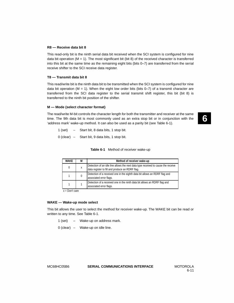
MC68HC05B6 MOTOROLA6-11
SERIAL COMMUNICATIONS INTERFACE
6
R8 — Receive data bit 8
This read-only bit is the ninth serial data bit received when the SCI system is configured for ninedata bit operation (M = 1). The most significant bit (bit 8) of the received character is transferredinto this bit at the same time as the remaining eight bits (bits 0–7) are transferred from the serialreceive shifter to the SCI receive data register.
T8 — Transmit data bit 8
This read/write bit is the ninth data bit to be transmitted when the SCI system is configured for ninedata bit operation (M = 1). When the eight low order bits (bits 0–7) of a transmit character aretransferred from the SCI data register to the serial transmit shift register, this bit (bit 8) istransferred to the ninth bit position of the shifter.
M — Mode (select character format)
The read/write M-bit controls the character length for both the transmitter and receiver at the sametime. The 9th data bit is most commonly used as an extra stop bit or in conjunction with the‘address mark’ wake-up method. It can also be used as a parity bit (see Table 6-1).
1 (set) – Start bit, 8 data bits, 1 stop bit.
0 (clear) – Start bit, 9 data bits, 1 stop bit.
WAKE — Wake-up mode select
This bit allows the user to select the method for receiver wake-up. The WAKE bit can be read orwritten to any time. See Table 6-1.
1 (set) – Wake-up on address mark.
0 (clear) – Wake-up on idle line.
Table 6-1 Method of receiver wake-up
WAKE M Method of receiver wake-up
0 xDetection of an idle line allows the next data type received to cause the receivedata register to fill and produce an RDRF flag.
1 0Detection of a received one in the eighth data bit allows an RDRF flag andassociated error flags.
1 1Detection of a received one in the ninth data bit allows an RDRF flag andassociated error flags.
x = Don’t care
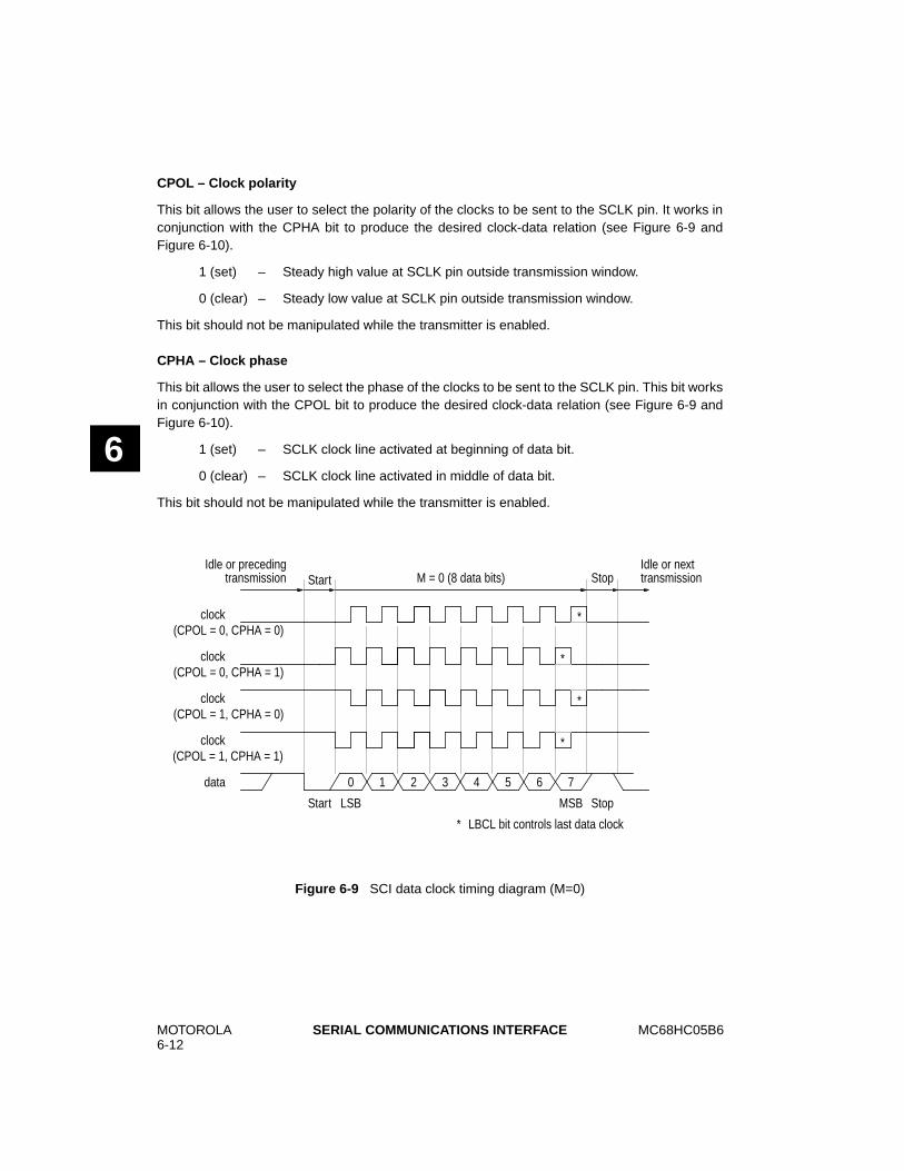
MOTOROLA6-12
MC68HC05B6SERIAL COMMUNICATIONS INTERFACE
6
CPOL – Clock polarity
This bit allows the user to select the polarity of the clocks to be sent to the SCLK pin. It works inconjunction with the CPHA bit to produce the desired clock-data relation (see Figure 6-9 andFigure 6-10).
1 (set) – Steady high value at SCLK pin outside transmission window.
0 (clear) – Steady low value at SCLK pin outside transmission window.
This bit should not be manipulated while the transmitter is enabled.
CPHA – Clock phase
This bit allows the user to select the phase of the clocks to be sent to the SCLK pin. This bit worksin conjunction with the CPOL bit to produce the desired clock-data relation (see Figure 6-9 andFigure 6-10).
1 (set) – SCLK clock line activated at beginning of data bit.
0 (clear) – SCLK clock line activated in middle of data bit.
This bit should not be manipulated while the transmitter is enabled.
Figure 6-9 SCI data clock timing diagram (M=0)
Idle or precedingtransmission
clock
StopStart
LSB
data
M = 0 (8 data bits)Idle or next
LBCL bit controls last data clock
transmission
clock
clock
clock
*
*
*
*
*
Start Stop
0 1 2 3 4 5 6
MSB
7
(CPOL = 0, CPHA = 0)
(CPOL = 0, CPHA = 1)
(CPOL = 1, CPHA = 0)
(CPOL = 1, CPHA = 1)
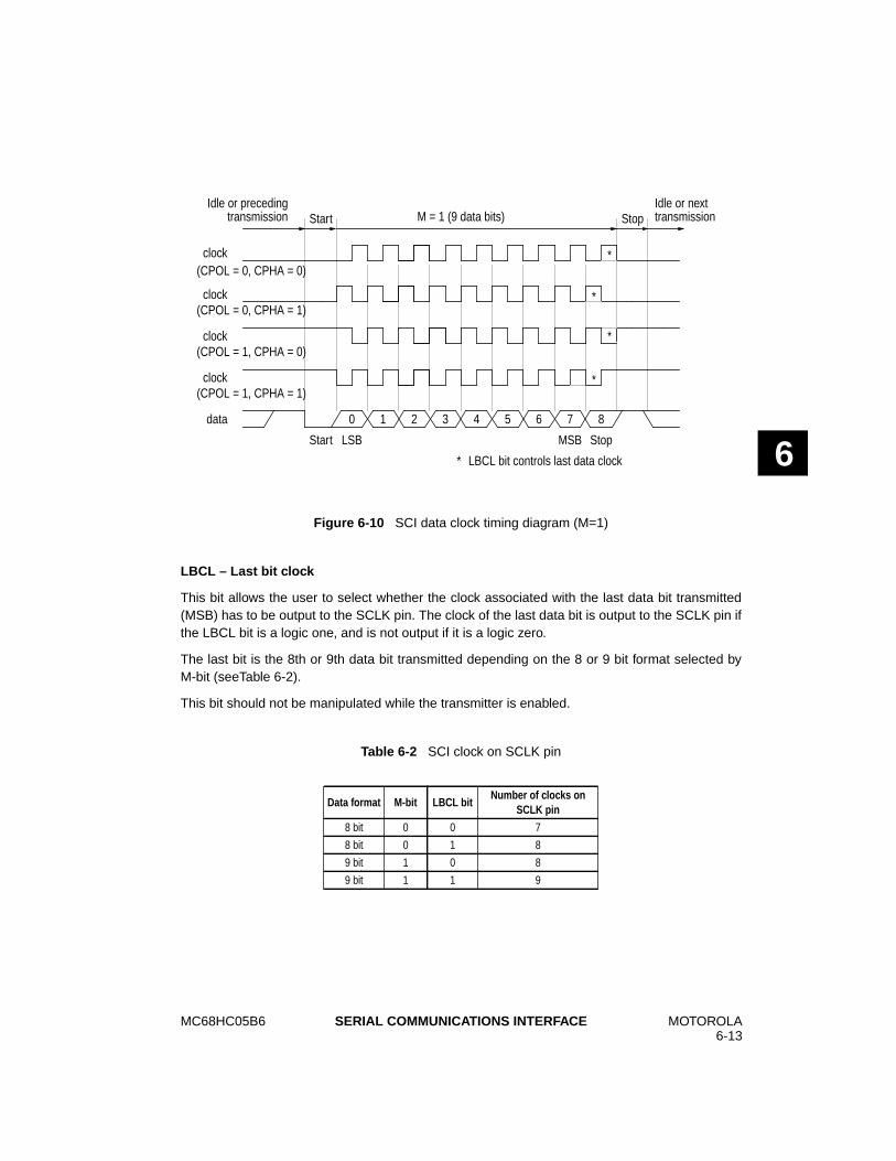
MC68HC05B6 MOTOROLA6-13
SERIAL COMMUNICATIONS INTERFACE
6
LBCL – Last bit clock
This bit allows the user to select whether the clock associated with the last data bit transmitted(MSB) has to be output to the SCLK pin. The clock of the last data bit is output to the SCLK pin ifthe LBCL bit is a logic one, and is not output if it is a logic zero.
The last bit is the 8th or 9th data bit transmitted depending on the 8 or 9 bit format selected byM-bit (seeTable 6-2).
This bit should not be manipulated while the transmitter is enabled.
Figure 6-10 SCI data clock timing diagram (M=1)
Table 6-2 SCI clock on SCLK pin
Data format M-bit LBCL bitNumber of clocks on
SCLK pin
8 bit 0 0 7
8 bit 0 1 8
9 bit 1 0 8
9 bit 1 1 9
Idle or precedingtransmission
clock
StopStart
LSB
data
M = 1 (9 data bits)Idle or next
LBCL bit controls last data clock
transmission
clock
clock
clock
*
*
*
*
Start Stop
0 1 2 3 4 5 6
MSB
7
*
8
(CPOL = 0, CPHA = 0)
(CPOL = 0, CPHA = 1)
(CPOL = 1, CPHA = 0)
(CPOL = 1, CPHA = 1)
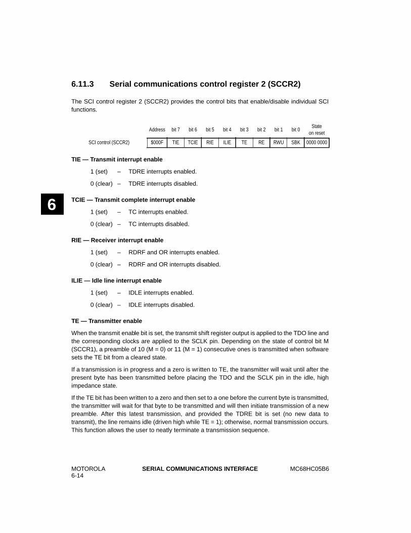
MOTOROLA6-14
MC68HC05B6SERIAL COMMUNICATIONS INTERFACE
6
6.11.3 Serial communications control register 2 (SCCR2)
The SCI control register 2 (SCCR2) provides the control bits that enable/disable individual SCIfunctions.
TIE — Transmit interrupt enable
1 (set) – TDRE interrupts enabled.
0 (clear) – TDRE interrupts disabled.
TCIE — Transmit complete interrupt enable
1 (set) – TC interrupts enabled.
0 (clear) – TC interrupts disabled.
RIE — Receiver interrupt enable
1 (set) – RDRF and OR interrupts enabled.
0 (clear) – RDRF and OR interrupts disabled.
ILIE — Idle line interrupt enable
1 (set) – IDLE interrupts enabled.
0 (clear) – IDLE interrupts disabled.
TE — Transmitter enable
When the transmit enable bit is set, the transmit shift register output is applied to the TDO line andthe corresponding clocks are applied to the SCLK pin. Depending on the state of control bit M(SCCR1), a preamble of 10 (M = 0) or 11 (M = 1) consecutive ones is transmitted when softwaresets the TE bit from a cleared state.
If a transmission is in progress and a zero is written to TE, the transmitter will wait until after thepresent byte has been transmitted before placing the TDO and the SCLK pin in the idle, highimpedance state.
If the TE bit has been written to a zero and then set to a one before the current byte is transmitted,the transmitter will wait for that byte to be transmitted and will then initiate transmission of a newpreamble. After this latest transmission, and provided the TDRE bit is set (no new data totransmit), the line remains idle (driven high while TE = 1); otherwise, normal transmission occurs.This function allows the user to neatly terminate a transmission sequence.
Address bit 7 bit 6 bit 5 bit 4 bit 3 bit 2 bit 1 bit 0State
on reset
SCI control (SCCR2) $000F TIE TCIE RIE ILIE TE RE RWU SBK 0000 0000
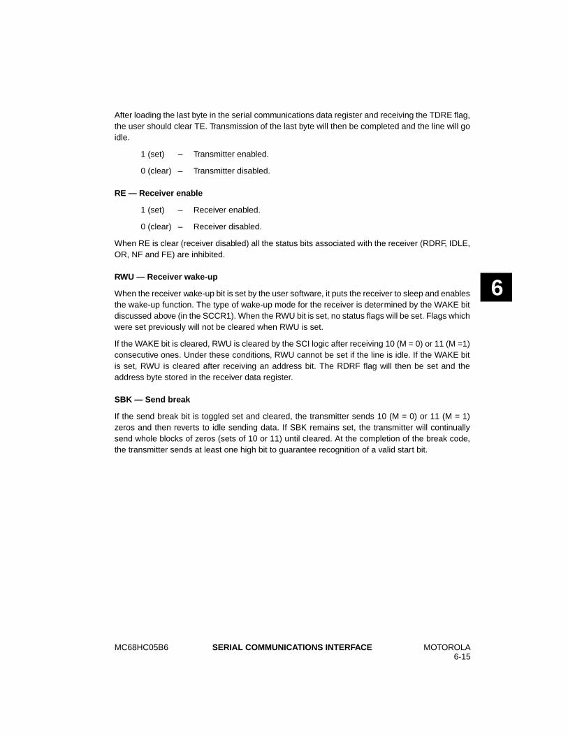
MC68HC05B6 MOTOROLA6-15
SERIAL COMMUNICATIONS INTERFACE
6
After loading the last byte in the serial communications data register and receiving the TDRE flag,the user should clear TE. Transmission of the last byte will then be completed and the line will goidle.
1 (set) – Transmitter enabled.
0 (clear) – Transmitter disabled.
RE — Receiver enable
1 (set) – Receiver enabled.
0 (clear) – Receiver disabled.
When RE is clear (receiver disabled) all the status bits associated with the receiver (RDRF, IDLE,OR, NF and FE) are inhibited.
RWU — Receiver wake-up
When the receiver wake-up bit is set by the user software, it puts the receiver to sleep and enablesthe wake-up function. The type of wake-up mode for the receiver is determined by the WAKE bitdiscussed above (in the SCCR1). When the RWU bit is set, no status flags will be set. Flags whichwere set previously will not be cleared when RWU is set.
If the WAKE bit is cleared, RWU is cleared by the SCI logic after receiving 10 (M = 0) or 11 (M =1)consecutive ones. Under these conditions, RWU cannot be set if the line is idle. If the WAKE bitis set, RWU is cleared after receiving an address bit. The RDRF flag will then be set and theaddress byte stored in the receiver data register.
SBK — Send break
If the send break bit is toggled set and cleared, the transmitter sends 10 (M = 0) or 11 (M = 1)zeros and then reverts to idle sending data. If SBK remains set, the transmitter will continuallysend whole blocks of zeros (sets of 10 or 11) until cleared. At the completion of the break code,the transmitter sends at least one high bit to guarantee recognition of a valid start bit.
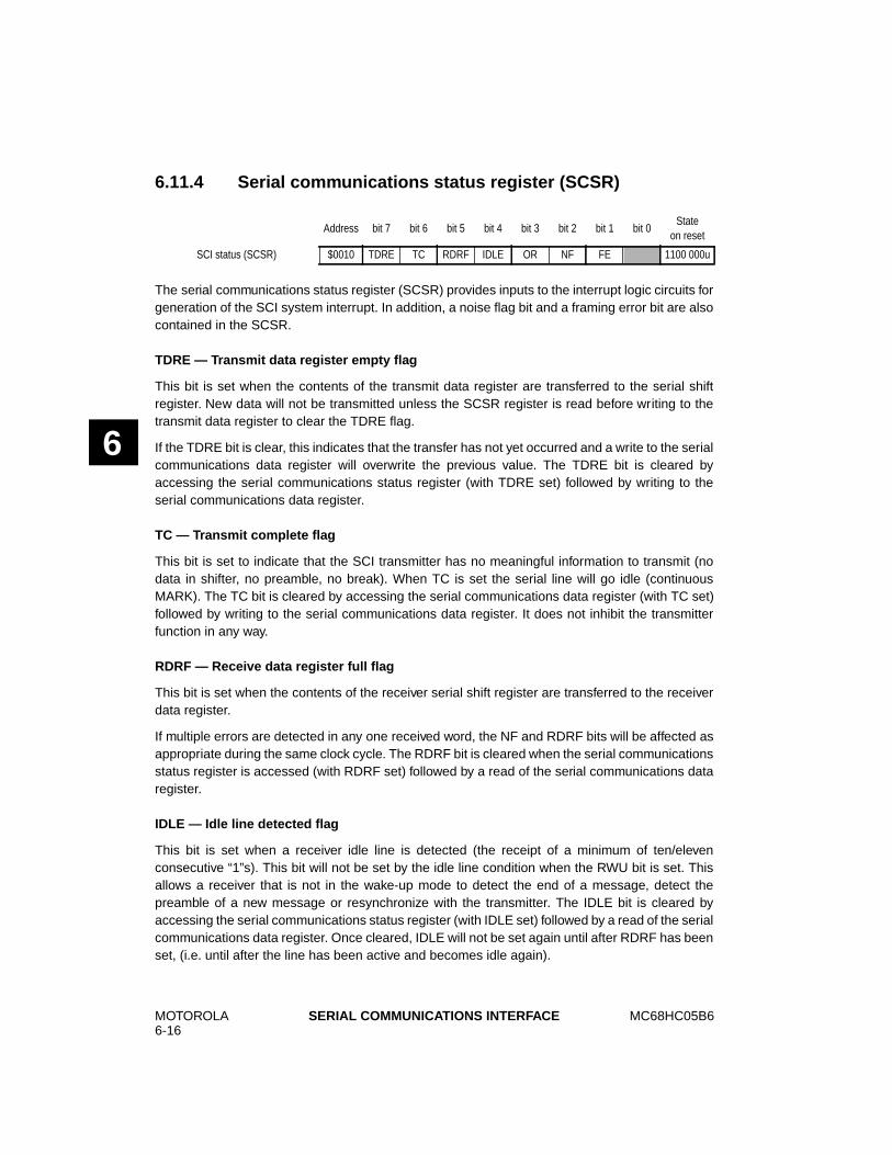
MOTOROLA6-16
MC68HC05B6SERIAL COMMUNICATIONS INTERFACE
6
6.11.4 Serial communications status register (SCSR)
The serial communications status register (SCSR) provides inputs to the interrupt logic circuits forgeneration of the SCI system interrupt. In addition, a noise flag bit and a framing error bit are alsocontained in the SCSR.
TDRE — Transmit data register empty flag
This bit is set when the contents of the transmit data register are transferred to the serial shiftregister. New data will not be transmitted unless the SCSR register is read before writing to thetransmit data register to clear the TDRE flag.
If the TDRE bit is clear, this indicates that the transfer has not yet occurred and a write to the serialcommunications data register will overwrite the previous value. The TDRE bit is cleared byaccessing the serial communications status register (with TDRE set) followed by writing to theserial communications data register.
TC — Transmit complete flag
This bit is set to indicate that the SCI transmitter has no meaningful information to transmit (nodata in shifter, no preamble, no break). When TC is set the serial line will go idle (continuousMARK). The TC bit is cleared by accessing the serial communications data register (with TC set)followed by writing to the serial communications data register. It does not inhibit the transmitterfunction in any way.
RDRF — Receive data register full flag
This bit is set when the contents of the receiver serial shift register are transferred to the receiverdata register.
If multiple errors are detected in any one received word, the NF and RDRF bits will be affected asappropriate during the same clock cycle. The RDRF bit is cleared when the serial communicationsstatus register is accessed (with RDRF set) followed by a read of the serial communications dataregister.
IDLE — Idle line detected flag
This bit is set when a receiver idle line is detected (the receipt of a minimum of ten/elevenconsecutive “1”s). This bit will not be set by the idle line condition when the RWU bit is set. Thisallows a receiver that is not in the wake-up mode to detect the end of a message, detect thepreamble of a new message or resynchronize with the transmitter. The IDLE bit is cleared byaccessing the serial communications status register (with IDLE set) followed by a read of the serialcommunications data register. Once cleared, IDLE will not be set again until after RDRF has beenset, (i.e. until after the line has been active and becomes idle again).
Address bit 7 bit 6 bit 5 bit 4 bit 3 bit 2 bit 1 bit 0State
on reset
SCI status (SCSR) $0010 TDRE TC RDRF IDLE OR NF FE 1100 000u
MC68HC05B6 MOTOROLA6-17
SERIAL COMMUNICATIONS INTERFACE
6
OR — Overrun error flag
This bit is set when a new byte is ready to be transferred from the receiver shift register to thereceiver data register and the receive data register is already full (RDRF bit is set). Data transferis inhibited until the RDRF bit is cleared. Data in the serial communications data register is validin this case, but additional data received during an overrun condition (including the byte causingthe overrun) will be lost.
The OR bit is cleared when the serial communications status register is accessed (with OR set)followed by a read of the serial communications data register.
NF — Noise error flag
This bit is set if there is noise on a ‘valid’ start bit, any of the data bits or on the stop bit. The NFbit is not set by noise on the idle line nor by invalid start bits. If there is noise, the NF bit is not setuntil the RDRF flag is set. Each data bit is sampled three times as described in Section 6.7.
The NF bit represents the status of the byte in the serial communications data register. For thebyte being received (shifted in) there will be also a ‘working’ noise flag, the value of which will betransferred to the NF bit when the serial data is loaded into the serial communications dataregister. The NF bit does not generate an interrupt because the RDRF bit gets set with NF andcan be used to generate the interrupt.
The NF bit is cleared when the serial communications status register is accessed (with NF set)followed by a read of the serial communications data register.
FE — Framing error flag
This bit is set when the word boundaries in the bit stream are not synchronized with the receiverbit counter (generated by the reception of a logic zero bit where a stop bit was expected). The FEbit reflects the status of the byte in the receive data register and the transfer from the receiveshifter to the receive data register is inhibited by an overrun. The FE bit is set during the samecycle as the RDRF bit but does not get set in the case of an overrun (OR). The framing error flaginhibits further transfer of data into the receive data register until it is cleared.
The FE bit is cleared when the serial communications status register is accessed (with FE set)followed by a read of the serial communications data register.
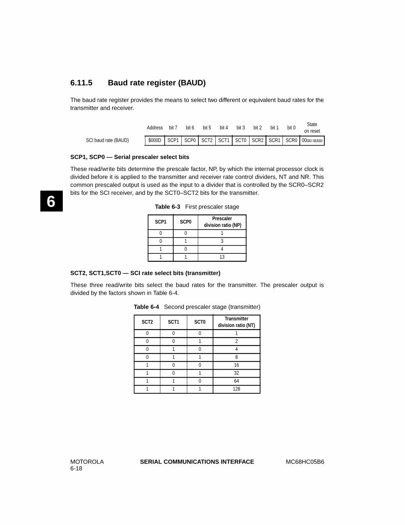
MOTOROLA6-18
MC68HC05B6SERIAL COMMUNICATIONS INTERFACE
6
6.11.5 Baud rate register (BAUD)
The baud rate register provides the means to select two different or equivalent baud rates for thetransmitter and receiver.
SCP1, SCP0 — Serial prescaler select bits
These read/write bits determine the prescale factor, NP, by which the internal processor clock isdivided before it is applied to the transmitter and receiver rate control dividers, NT and NR. Thiscommon prescaled output is used as the input to a divider that is controlled by the SCR0–SCR2bits for the SCI receiver, and by the SCT0–SCT2 bits for the transmitter.
SCT2, SCT1,SCT0 — SCI rate select bits (transmitter)
These three read/write bits select the baud rates for the transmitter. The prescaler output isdivided by the factors shown in Table 6-4.
Address bit 7 bit 6 bit 5 bit 4 bit 3 bit 2 bit 1 bit 0State
on reset
SCI baud rate (BAUD) $000D SCP1 SCP0 SCT2 SCT1 SCT0 SCR2 SCR1 SCR0 00uu uuuu
Table 6-3 First prescaler stage
SCP1 SCP0Prescaler
division ratio (NP)
0 0 1
0 1 3
1 0 4
1 1 13
Table 6-4 Second prescaler stage (transmitter)
SCT2 SCT1 SCT0Transmitter
division ratio (NT)
0 0 0 1
0 0 1 2
0 1 0 4
0 1 1 8
1 0 0 16
1 0 1 32
1 1 0 64
1 1 1 128
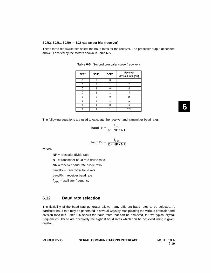
MC68HC05B6 MOTOROLA6-19
SERIAL COMMUNICATIONS INTERFACE
6
SCR2, SCR1, SCR0 — SCI rate select bits (receiver)
These three read/write bits select the baud rates for the receiver. The prescaler output describedabove is divided by the factors shown in Table 6-5.
The following equations are used to calculate the receiver and transmitter baud rates:
where:
NP = prescaler divide ratio
NT = transmitter baud rate divide ratio
NR = receiver baud rate divide ratio
baudTx = transmitter baud rate
baudRx = receiver baud rate
fOSC = oscillator frequency
6.12 Baud rate selection
The flexibility of the baud rate generator allows many different baud rates to be selected. Aparticular baud rate may be generated in several ways by manipulating the various prescaler anddivision ratio bits. Table 6-6 shows the baud rates that can be achieved, for five typical crystalfrequencies. These are effectively the highest baud rates which can be achieved using a givencrystal.
Table 6-5 Second prescaler stage (receiver)
SCR2 SCR1 SCR0Receiver
division ratio (NR)
0 0 0 1
0 0 1 2
0 1 0 4
0 1 1 8
1 0 0 16
1 0 1 32
1 1 0 64
1 1 1 128
baudTxfosc
32 NP NT• •----------------------------------=
baudRxfosc
32 NP NR• •-----------------------------------=
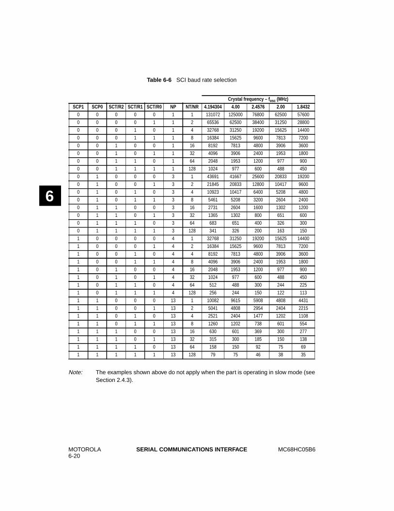
MOTOROLA6-20
MC68HC05B6SERIAL COMMUNICATIONS INTERFACE
6
Note: The examples shown above do not apply when the part is operating in slow mode (seeSection 2.4.3).
Table 6-6 SCI baud rate selection
Crystal frequency – f osc (MHz)
SCP1 SCP0 SCT/R2 SCT/R1 SCT/R0 NP NT/NR 4.194304 4.00 2.4576 2.00 1.8432
0 0 0 0 0 1 1 131072 125000 76800 62500 57600
0 0 0 0 1 1 2 65536 62500 38400 31250 28800
0 0 0 1 0 1 4 32768 31250 19200 15625 14400
0 0 0 1 1 1 8 16384 15625 9600 7813 7200
0 0 1 0 0 1 16 8192 7813 4800 3906 3600
0 0 1 0 1 1 32 4096 3906 2400 1953 1800
0 0 1 1 0 1 64 2048 1953 1200 977 900
0 0 1 1 1 1 128 1024 977 600 488 450
0 1 0 0 0 3 1 43691 41667 25600 20833 19200
0 1 0 0 1 3 2 21845 20833 12800 10417 9600
0 1 0 1 0 3 4 10923 10417 6400 5208 4800
0 1 0 1 1 3 8 5461 5208 3200 2604 2400
0 1 1 0 0 3 16 2731 2604 1600 1302 1200
0 1 1 0 1 3 32 1365 1302 800 651 600
0 1 1 1 0 3 64 683 651 400 326 300
0 1 1 1 1 3 128 341 326 200 163 150
1 0 0 0 0 4 1 32768 31250 19200 15625 14400
1 0 0 0 1 4 2 16384 15625 9600 7813 7200
1 0 0 1 0 4 4 8192 7813 4800 3906 3600
1 0 0 1 1 4 8 4096 3906 2400 1953 1800
1 0 1 0 0 4 16 2048 1953 1200 977 900
1 0 1 0 1 4 32 1024 977 600 488 450
1 0 1 1 0 4 64 512 488 300 244 225
1 0 1 1 1 4 128 256 244 150 122 113
1 1 0 0 0 13 1 10082 9615 5908 4808 4431
1 1 0 0 1 13 2 5041 4808 2954 2404 2215
1 1 0 1 0 13 4 2521 2404 1477 1202 1108
1 1 0 1 1 13 8 1260 1202 738 601 554
1 1 1 0 0 13 16 630 601 369 300 277
1 1 1 0 1 13 32 315 300 185 150 138
1 1 1 1 0 13 64 158 150 92 75 69
1 1 1 1 1 13 128 79 75 46 38 35

MC68HC05B6 MOTOROLA6-21
SERIAL COMMUNICATIONS INTERFACE
6
6.13 SCI during STOP mode
When the MCU enters STOP mode, the baud rate generator driving the receiver and transmitteris shut down. This stops all SCI activity. Both the receiver and the transmitter are unable tooperate.
If the STOP instruction is executed during a transmitter transfer, that transfer is halted. WhenSTOP mode is exited as a result of an external interrupt, that particular transmission resumes.
If the receiver is receiving data when the STOP instruction is executed, received data sampling isstopped (baud generator stops) and the rest of the data is lost.
Warning: For the above reasons, all SCI transactions should be in the idle state when the STOPinstruction is executed.
6.14 SCI during WAIT mode
The SCI system is not affected by WAIT mode and continues normal operation. Any valid SCIinterrupt will wake-up the system. If required, the SCI system can be disabled prior to enteringWAIT mode by writing a zero to the transmitter and receiver enable bits in the serialcommunication control register 2 at $000F. This action will result in a reduction of powerconsumption during WAIT mode.

MOTOROLA6-22
MC68HC05B6SERIAL COMMUNICATIONS INTERFACE
THIS PAGE INTENTIONALLY LEFT BLANK
6
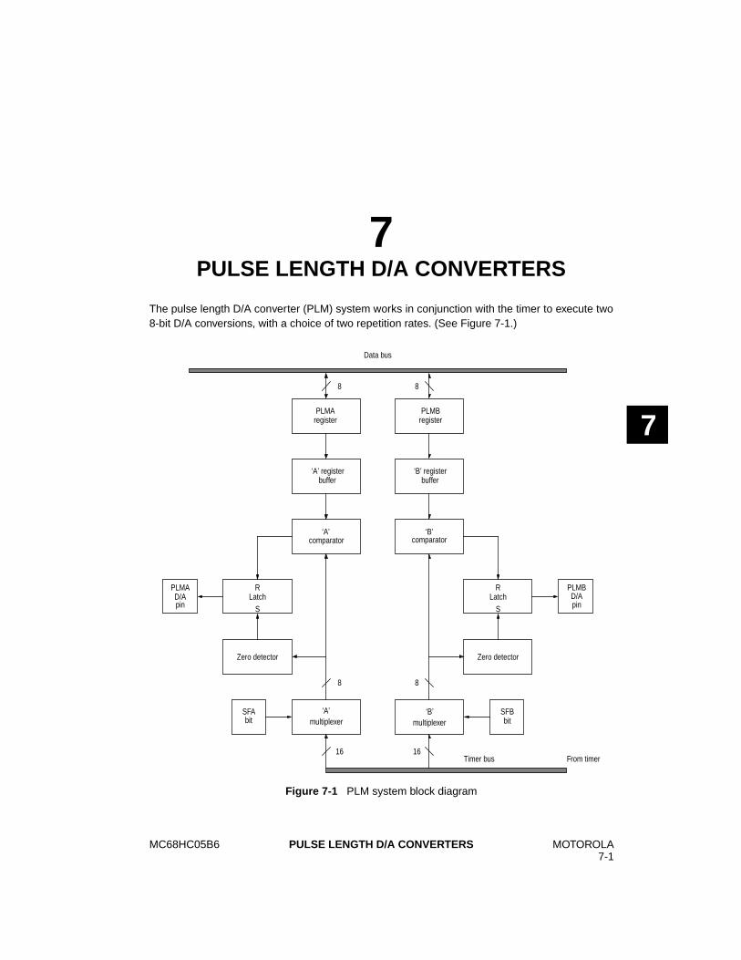
MC68HC05B6 MOTOROLA7-1
PULSE LENGTH D/A CONVERTERS
7
7PULSE LENGTH D/A CONVERTERS
The pulse length D/A converter (PLM) system works in conjunction with the timer to execute two8-bit D/A conversions, with a choice of two repetition rates. (See Figure 7-1.)
Figure 7-1 PLM system block diagram
PLMAregister
PLMB
‘A’ registerbuffer
‘B’ register
‘A’comparator
‘B’
Latch
Zero detector
SFAbit
SFB
D/Apin
Timer bus From timer
Data bus
8
16
multiplexer‘A’ ‘B’
buffer
register
comparator
multiplexer
PLMA
PLMB
D/AR
S
bit
Zero detector
8
16
8 8
pinLatch
R
S

MOTOROLA7-2
MC68HC05B6PULSE LENGTH D/A CONVERTERS
7
The D/A converter has two data registers associated with it, PLMA and PLMB.
This is a dual 8-bit resolution D/A converter associated with two output pins (PLMA and PLMB).The outputs are pulse length modulated signals whose duty cycle ratio may be modified. Thesesignals can be used directly as PLMs, or the filtered average may be used as general purposeanalog outputs.
The longest repetition period is 4096 times the programmable timer clock period (CPU clockmultiplied by four), and the shortest repetition period is 256 times the programmable timer clockperiod (the repetition rate frequencies for a 4 MHz crystal are 122 Hz and 1953 Hz respectively).Registers PLMA ($0A) and PLMB ($0B) are associated with the pulse length values of the twocounters. A value of $00 loaded into these registers results in a continuously low output on thecorresponding D/A output pin. A value of $80 results in a 50% duty cycle output, and so on, to themaximum value $FF corresponding to an output which is at ‘1’ for 255/256 of the cycle. When theMCU makes a write to register PLMA or PLMB the new value will only be picked up by the D/Aconverters at the end of a complete cycle of conversion. This results in a monotonic change of theDC component at the output without overshoots or vicious starts (a vicious start is an output whichgives totally erroneous PLM during the period immediately following an update of the PLM D/Aregisters). This feature is achieved by double buffering of the PLM D/A registers. Examples ofPWM output waveforms are shown in Figure 7-2.
Address bit 7 bit 6 bit 5 bit 4 bit 3 bit 2 bit 1 bit 0State
on reset
Pulse length modulation A (PLMA) $000A 0000 0000
Pulse length modulation B (PLMB) $000B 0000 0000
Figure 7-2 PLM output waveform examples
256 T
255 T
128 T
T
$80
$FF
T = 4 CPU clocks in fast mode and 64 CPU clocks in slow mode
128 T
T
$00
$01
255 T
MC68HC05B6 MOTOROLA7-3
PULSE LENGTH D/A CONVERTERS
7
Note: Since the PLM system uses the timer counter, PLM results will be affected while resettingthe timer counter. Both D/A registers are reset to $00 during power-on or external reset.WAIT mode does not affect the output waveform of the D/A converters.
7.1 Miscellaneous register
SFA — Slow or fast mode selection for PLMA
This bit allows the user to select the slow or fast mode of the PLMA pulse length modulationoutput.
1 (set) – Slow mode PLMA (4096 x timer clock period).
0 (clear) – Fast mode PLMA (256 x timer clock period).
SFB — Slow or fast mode selection for PLMB
This bit allows the user to select the slow or fast mode of the PLMB pulse length modulationoutput.
1 (set) – Slow mode PLMB (4096 x timer clock period).
0 (clear) – Fast mode PLMB (256 x timer clock period).
The highest speed of the PLM system corresponds to the frequency of the TOF bit being set,multiplied by 256. The lowest speed of the PLM system corresponds to the frequency of the TOFbit being set, multiplied by 16. Because the SFA bit and SFB bit are not double buffered, it ismandatory to set them to the desired values before writing to the PLM registers; not doing so couldtemporarily give incorrect values at the PLM outputs.
SM — Slow mode
1 (set) – The system runs at a bus speed 16 times lower than normal(fOSC/32). SLOW mode affects all sections of the device, includingSCI, A/D and timer.
0 (clear) – The system runs at normal bus speed (fOSC/2).
Address bit 7 bit 6 bit 5 bit 4 bit 3 bit 2 bit 1 bit 0State
on reset
Miscellaneous $000C POR INTP INTN INTE SFA SFB SM WDOG ?001 000?
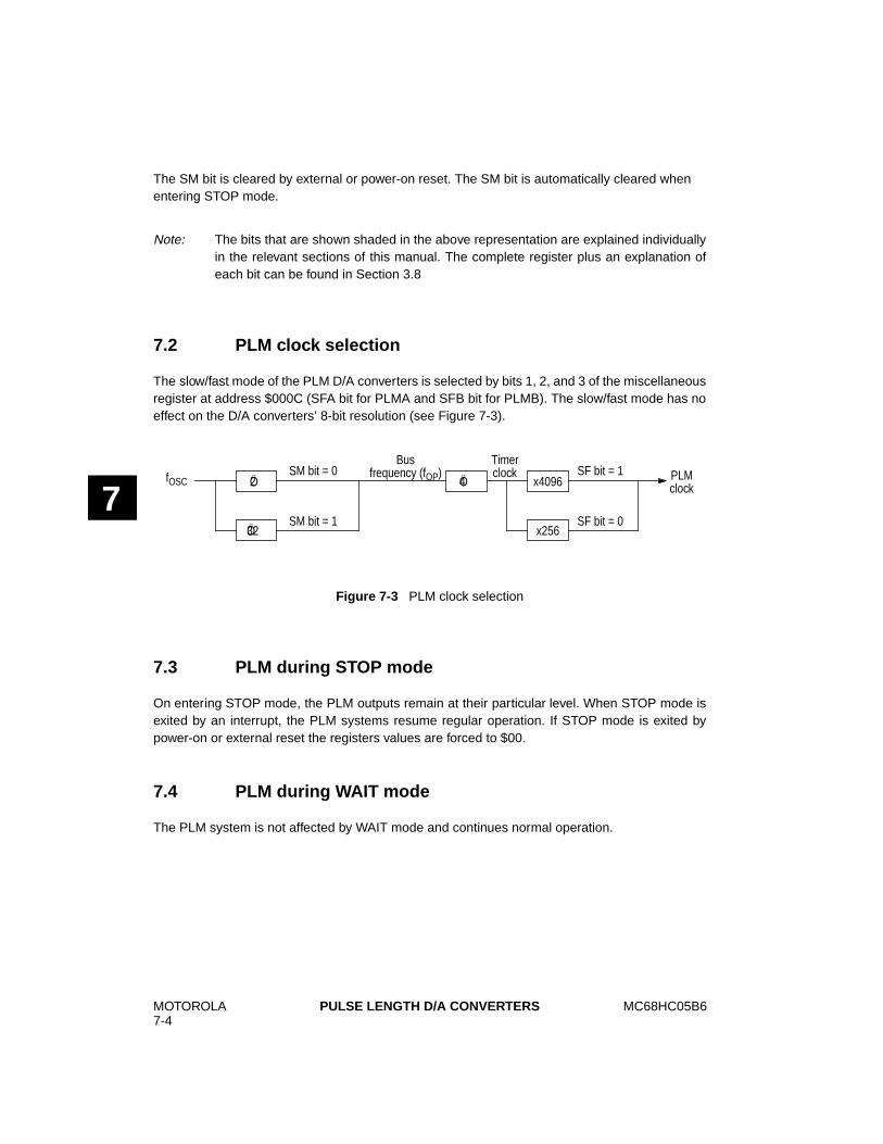
MOTOROLA7-4
MC68HC05B6PULSE LENGTH D/A CONVERTERS
7
The SM bit is cleared by external or power-on reset. The SM bit is automatically cleared whenentering STOP mode.
Note: The bits that are shown shaded in the above representation are explained individuallyin the relevant sections of this manual. The complete register plus an explanation ofeach bit can be found in Section 3.8
7.2 PLM clock selection
The slow/fast mode of the PLM D/A converters is selected by bits 1, 2, and 3 of the miscellaneousregister at address $000C (SFA bit for PLMA and SFB bit for PLMB). The slow/fast mode has noeffect on the D/A converters’ 8-bit resolution (see Figure 7-3).
7.3 PLM during STOP mode
On entering STOP mode, the PLM outputs remain at their particular level. When STOP mode isexited by an interrupt, the PLM systems resume regular operation. If STOP mode is exited bypower-on or external reset the registers values are forced to $00.
7.4 PLM during WAIT mode
The PLM system is not affected by WAIT mode and continues normal operation.
Figure 7-3 PLM clock selection
fOSC Ö2
Ö32
SM bit = 0
SM bit = 1
Ö4 x4096
x256
SF bit = 1
SF bit = 0
Timerclock PLM
clock
Busfrequency (fOP)
MC68HC05B6 MOTOROLA8-1
ANALOG TO DIGITAL CONVERTER
8
8ANALOG TO DIGITAL CONVERTER
The analog to digital converter system consists of a single 8-bit successive approximationconverter and a sixteen channel multiplexer. Eight of the channels are connected to thePD0/AN0 – PD7/AN7 pins of the MC68HC05B6 and the other eight channels are dedicated tointernal reference points for test functions. The channel input pins do not have any internal outputdriver circuitry connected to them because such circuitry would load the analog input signals dueto output buffer leakage current. There is one 8-bit result data register (address $08) and one 8-bitstatus/control register (address $09).
The A/D converter is ratiometric and two dedicated pins, VRH and VRL, are used to supply thereference voltage levels for all analog inputs. These pins are used in preference to the systempower supply lines because any voltage drops in the bonding wires of the heavily loaded supplypins could degrade the accuracy of the A/D conversion. An input voltage equal to or greater thanVRH converts to $FF (full scale) with no overflow indication and an input voltage equal to VRLconverts to $00.
The A/D converter can operate from either the bus clock or an internal RC type oscillator. Theinternal RC type oscillator is activated by the ADRC bit in the A/D status/control register (ADSTAT)and can be used to give a sufficiently high clock rate to the A/D converter when the bus speed is toolow to provide accurate results. When the A/D converter is not being used it can be disconnected,by clearing the ADON bit in the ADSTAT register, in order to save power (see Section 8.2.3).
For further information on A/D converter operation please refer to the M68HC11 ReferenceManual — M68HC11RM/AD.
8.1 A/D converter operation
The A/D converter consists of an analog multiplexer, an 8-bit digital to analog converter capacitorarray, a comparator and a successive approximation register (SAR) (see Figure 8-1).
There are eleven options that can be selected by the multiplexer; AN0–AN7, VRH, (VRH+VRL)/2or VRL. Selection is done via the CHx bits in the ADSTAT register (see Section 8.2.3). AN0–AN7are the only input points for A/D conversion operations; the others are reference points that canbe used for test purposes.
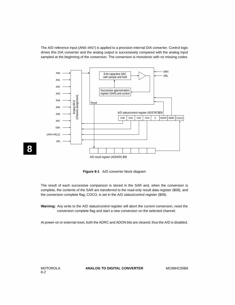
MOTOROLA8-2
MC68HC05B6ANALOG TO DIGITAL CONVERTER
8
The A/D reference input (AN0–AN7) is applied to a precision internal D/A converter. Control logicdrives this D/A converter and the analog output is successively compared with the analog inputsampled at the beginning of the conversion. The conversion is monotonic with no missing codes.
The result of each successive comparison is stored in the SAR and, when the conversion iscomplete, the contents of the SAR are transferred to the read-only result data register ($08), andthe conversion complete flag, COCO, is set in the A/D status/control register ($09).
Warning: Any write to the A/D status/control register will abort the current conversion, reset theconversion complete flag and start a new conversion on the selected channel.
At power-on or external reset, both the ADRC and ADON bits are cleared; thus the A/D is disabled.
Figure 8-1 A/D converter block diagram
AN0
VRH
(VRH+VRL)/2
VRL
Anal
og M
UX
A/D result register (ADDATA) $08
8-bit capacitive DACwith sample and hold
VRHVRL
Result
A/D status/control register (ADSTAT)$09
(Cha
nnel
ass
ignm
ent)
COCOADRCADON0CH3CH2CH1CH0
AN1
AN2
AN3
AN4
AN5
AN6
AN7
Successive approximationregister (SAR) and control
MC68HC05B6 MOTOROLA8-3
ANALOG TO DIGITAL CONVERTER
8
8.2 A/D registers
8.2.1 Port D data register (PORTD)
Port D is an input-only port which routes the eight analog inputs to the A/D converter. When theA/D converter is disabled, the pins are configured as standard input-only port pins, which can beread via the port D data register.
Note: When the A/D function is enabled, pins PD0–PD7 will act as analog inputs. Using a pinor pins as A/D inputs does not affect the ability to read port D as static inputs; however,reading port D during an A/D conversion sequence may inject noise on the analoginputs and result in reduced accuracy of the A/D result.Performing a digital read of port D with levels other than VDD or VSS on the pins willresult in greater power dissipation during the read cycle, and may give unpredictableresults on the corresponding port D pins.
8.2.2 A/D result data register (ADDATA )
ADDATA is a read-only register which is used to store the results of A/D conversions. Each resultis loaded into the register from the SAR and the conversion complete flag, COCO, in the ADSTATregister is set.
Address bit 7 bit 6 bit 5 bit 4 bit 3 bit 2 bit 1 bit 0State
on reset
Port D data (PORTD) $0003 PD7 PD6 PD5 PD4 PD3 PD2 PD1 PD0 Undefined
Address bit 7 bit 6 bit 5 bit 4 bit 3 bit 2 bit 1 bit 0State
on reset
A/D data (ADDATA) $0008 0000 0000
MOTOROLA8-4
MC68HC05B6ANALOG TO DIGITAL CONVERTER
8
8.2.3 A/D status/control register (ADSTAT)
COCO — Conversion complete flag
1 (set) – COCO is set each time a conversion is complete, allowing the newresult to be read from the A/D result data register ($08). Theconverter then starts a new conversion.
0 (clear) – COCO is cleared by reading the result data register or writing to thestatus/control register.
Reset clears the COCO flag.
ADRC — A/D RC oscillator control
The ADRC bit allows the user to control the A/D RC oscillator, which is used to provide asufficiently high clock rate to the A/D to ensure accuracy when the chip is running at low speeds.
1 (set) – When the ADRC bit is set, the A/D RC oscillator is turned on and, ifADON is set, the A/D runs from the RC oscillator clock. See Table 8-1.
0 (clear) – When the ADRC bit is cleared, the A/D RC oscillator is turned-offand, if ADON is set, the A/D runs from the CPU clock.
When the A/D RC oscillator is turned on, it takes a time tADRC to stabilize (see Table 11-7 andTable 11-8). During this time A/D conversion results may be inaccurate.
Note: If the MCU bus clock falls below 1MHz, the A/D RC oscillator should be switched on.
Power-on or external reset clears the ADRC bit.
Address bit 7 bit 6 bit 5 bit 4 bit 3 bit 2 bit 1 bit 0State
on reset
A/D status/control (ADSTAT) $0009 COCO ADRC ADON 0 CH3 CH2 CH1 CH0 0000 0000
Table 8-1 A/D clock selection
ADRC ADONRC
oscillatorA/D
converterComments
0 0 OFF OFF A/D switched off.
0 1 OFF ON A/D using CPU clock.
1 0 ON OFF Allows the RC oscillator to stabilize.
1 1 ON ON A/D using RC oscillator clock.
MC68HC05B6 MOTOROLA8-5
ANALOG TO DIGITAL CONVERTER
8
ADON — A/D converter on
The ADON bit allows the user to enable/disable the A/D converter.
1 (set) – A/D converter is switched on.
0 (clear) – A/D converter is switched off.
When the A/D converter is switched on, it takes a time tADON for the current sources to stabilize(see Table 11-7 and Table 11-8). During this time A/D conversion results may be inaccurate.
Power-on or external reset will clear the ADON bit, thus disabling the A/D converter.
CH3–CH0 — A/D channels 3, 2, 1 and 0
The CH3–CH0 bits allow the user to determine which channel of the A/D converter multiplexer isselected. See Table 8-2 for channel selection.
Reset clears the CH0–CH3 bits.
8.3 A/D converter during STOP mode
When the MCU enters STOP mode with the A/D converter turned on, the A/D clocks are stoppedand the A/D converter is disabled for the duration of STOP mode, including the 4064 cyclesstart-up time. If the A/D RC oscillator is in operation it will also be disabled.
Table 8-2 A/D channel assignment
CH3 CH2 CH1 CH0 Channel selected
0 0 0 0 AN0
0 0 0 1 AN1
0 0 1 0 AN2
0 0 1 1 AN3
0 1 0 0 AN4
0 1 0 1 AN5
0 1 1 0 AN6
0 1 1 1 AN7
1 0 0 0 VRH pin (high)
1 0 0 1 (VRH + VRL) / 2
1 0 1 0 VRL pin (low)
1 0 1 1 VRL pin (low)
1 1 0 0 VRL pin (low)
1 1 0 1 VRL pin (low)
1 1 1 0 VRL pin (low)
1 1 1 1 VRL pin (low)
MOTOROLA8-6
MC68HC05B6ANALOG TO DIGITAL CONVERTER
8
8.4 A/D converter during WAIT mode
The A/D converter is not affected by WAIT mode and continues normal operation.
In order to reduce power consumption the A/D converter can be disconnected, under softwarecontrol using the ADON bit and the ADRC bit in the A/D status/control register at $0009, beforeentering WAIT mode.
8.5 Port D analog input
The external analog voltage value to be processed by the A/D converter is sampled on an internalcapacitor through a resistive path, provided by input-selection switches and a sampling aperturetime switch, as shown in Figure 8-2. Sampling time is limited to 12 bus clock cycles. Aftersampling, the analog value is stored on the capacitor and held until the end of conversion. Duringthis hold time, the analog input is disconnected from the internal A/D system and the externalvoltage source sees a high impedance input.
The equivalent analog input during sampling is an RC low-pass filter with a minimum resistanceof 50 k½ and a capacitance of at least 10pF. It should be noted that these are typical valuesmeasured at room temperature.
Figure 8-2 Electrical model of an A/D input pin
Analoginput
pin
Input protection device
VRL
< 2pF
+ ~20V- ~0.7V
400 nAjunctionleakage
50k½
10pF
DACcapacitance
Note: The analog switch is closed during the 12 cycle sample time only.
MC68HC05B6 MOTOROLA9-1
RESETS AND INTERRUPTS
9
9RESETS AND INTERRUPTS
9.1 Resets
The MC68HC05B6 can be reset in three ways: by the initial power-on reset function, by an activelow input to the RESET pin or by a computer operating properly (COP) watchdog reset. Any ofthese resets will cause the program to go to its starting address, specified by the contents ofmemory locations $1FFE and $1FFF, and cause the interrupt mask bit in the condition coderegister to be set.
Figure 9-1 Reset timing diagram
VDD
RESET
1FFF1FFE1FFE1FFENew
1FFF1FFE1FFE1FFE PC
OSC1
NewPC
Internal
Internalprocessor clock
1FFE
Opcode
NewPCL
NewPCH
tVDDR
Opcode
NewPCL
NewPCH
address bus
Internaldata bus
tOXOV
tCYCtPORL
1FFE
Programexecutionbegins
Programexecutionbegins
tRL(or tDOGL)(Internal power-on reset) (External hardware reset)
VDD threshold (1-2V typical)
Reset sequence Reset sequence
MOTOROLA9-2
MC68HC05B6RESETS AND INTERRUPTS
9
9.1.1 Power-on reset
A power-on reset occurs when a positive transition is detected on VDD. The power-on resetfunction is strictly for power turn-on conditions and should not be used to detect drops in the powersupply voltage. The power-on circuitry provides a stabilization delay (tPORL) from when theoscillator becomes active. If the external RESET pin is low at the end of this delay then theprocessor remains in the reset state until RESET goes high. The user must ensure that the voltageon VDD has risen to a point where the MCU can operate properly by the time tPORL has elapsed.If there is doubt, the external RESET pin should remain low until the voltage on VDD has reachedthe specified minimum operating voltage. This may be accomplished by connecting an externalRC circuit to this pin to generate a power-on reset (POR). In this case, the time constant must begreat enough to allow the oscillator circuit to stabilize.
During power-on reset, the RESET pin is driven low during a tPORL delay start-up sequence. tPORL isdefined by a user specified mask option to be either 16 cycles or 4064 cycles (see Section 1.2).
A software distinction between a power-on reset and an external reset can be made using thePOR bit in the miscellaneous register (see Section 9.1.2).
9.1.2 Miscellaneous register
POR — Power-on reset bit
This bit is set each time the device is powered on. Therefore, the state of the POR bit allows theuser to make a software distinction between a power-on and an external reset. This bit cannot beset by software and is cleared by writing it to zero.
1 (set) – A power-on reset has occurred.
0 (clear) – No power-on reset has occurred.
Note: The bits shown shaded in the above representation are explained individually in therelevant sections of this manual. The complete register plus an explanation of each bitcan be found in Section 3.8.
(1) The POR bit is set each time there is a power-on reset.
(2) The state of the WDOG bit after reset is dependent on the mask option selected; 1=watchdog enabled, 0=watchdog disabled.
Address bit 7 bit 6 bit 5 bit 4 bit 3 bit 2 bit 1 bit 0State
on reset
Miscellaneous $000C POR(1) INTP INTN INTE SFA SFB SM WDOG(2) ?001 000?
MC68HC05B6 MOTOROLA9-3
RESETS AND INTERRUPTS
9
9.1.3 RESET pin
When the oscillator is running in a stable condition, the MCU is reset when a logic zero is appliedto the RESET input for a minimum period of 1.5 machine cycles (tCYC). An internal Schmitt Triggeris used to improve noise immunity on this pin. When the RESET pin goes high, the MCU willresume operation on the following cycle. When a reset condition occurs internally, i.e. from PORor the COP watchdog, the RESET pin provides an active-low open drain output signal which maybe used to reset external hardware. Current limitation to protect the pull-down device is providedin case an RC type external reset circuit is used.
9.1.4 Computer operating properly (COP) watchdog reset
The watchdog counter system consists of a divide-by-8 counter, preceded by a fixed divide-by-4and a fixed divide-by-256 prescaler, plus control logic as shown in Figure 9-2. The divide-by-8counter can be reset by software.
Warning: The input to the watchdog system is derived from the carry output of bit 7 of the freerunning timer counter. Therefore, a reset of the timer may affect the period of thewatchdog timeout.
The watchdog system can be automatically enabled, following power-on or external reset, via amask option (see Section 1.2), or it can be enabled by software by writing a ‘1’ to the WDOG bitin the miscellaneous register at $000C (see Section 9.1.2). Once enabled, the watchdog system
Figure 9-2 Watchdog system block diagram
Ö 256(Bit 7 of free
fosc/2
fosc/32
Main CPU
Ö 8 watchdogcounter
WDOG bit Control logic
Latch
+
Reset
Schmitt Inputprotectiontrigger
pin
Power-onS
R
Enab
le
Res
et
clock
Ö 4prescaler
running counter)
MOTOROLA9-4
MC68HC05B6RESETS AND INTERRUPTS
9
cannot be disabled by software (writing a ‘zero’ to the WDOG bit has no effect at any time). Inaddition, the WDOG bit acts as a reset mechanism for the watchdog counter. Writing a ‘1’ to thisbit clears the counter to its initial value and prevents a watchdog timeout.
WDOG — Watchdog enable/disable
The WDOG bit can be used to enable the watchdog timer previously disabled by a mask option.Following a watchdog reset the state of the WDOG bit is as defined by the mask option specified.
1 (set) – Watchdog enabled and counter cleared.
0 (clear) – The watchdog cannot be disabled by software; writing a zero to thisbit has no effect.
The divide-by-8 watchdog counter will generate a main reset of the chip when it reaches its finalstate; seven clocks are necessary to bring the watchdog counter from its clear state to its finalstate. This reset appears after time tDOG since the last clear or since the enable of the watchdogcounter system. The watchdog counter, therefore, has to be cleared periodically, by software, witha period less than tDOG.
The reset generated by the watchdog system is apparent at the RESET pin (see Figure 9-2). TheRESET pin level is re-entered in the control logic, and when it has been maintained at level ‘zero’for a minimum of tDOGL, the RESET pin is released.
9.1.4.1 COP watchdog during STOP mode
The STOP instruction is inhibited when the watchdog system is enabled. If a STOP instruction isexecuted while the watchdog system is enabled, then a watchdog reset will occur as if there werea watchdog timeout. In the case of a watchdog reset due to a STOP instruction, the oscillator willnot be affected, thus there will be no tPORL cycles start-up delay. On start-up, the watchdog will beconfigured according to the user specified mask option.
9.1.4.2 COP watchdog during WAIT mode
The state of the watchdog during WAIT mode is selected via a mask option (see Section 1.2) tobe one of the options below:
Watchdog enabled — the watchdog counter will continue to operate during WAIT mode and areset will occur after time tDOG.
Watchdog disabled — on entering WAIT mode, the watchdog counter system is reset anddisabled. On exiting WAIT mode the counter resumes normal operation.
MC68HC05B6 MOTOROLA9-5
RESETS AND INTERRUPTS
9
9.1.5 Functions affected by reset
When processing stops within the MCU for any reason, i.e. power-on reset, external reset or theexecution of a STOP or WAIT instruction, various internal functions of the MCU are affected.Table 9-1 shows the resulting action of any type of system reset, but not necessarily in the orderin which they occur.
Table 9-1 Effect of RESET, POR, STOP and WAIT
Function/effect RESET POR WAIT STOP
Timer prescaler set to zero x x – –
Timer counter set to $FFFC x x – –
All timer enable bits cleared (disable) x x – –
Data direction registers cleared (inputs) x x – –
Stack pointer set to $00FF x x – –
Force internal address bus to restart x x – –
Vector $1FFE, $1FFF x x – –
Interrupt mask bit (I-bit CCR) set to 1 x x – –
Interrupt mask bit (I-bit CCR) cleared – – x x
Set interrupt enable bit (INTE) x x – –
Set POR bit in miscellaneous register – x – –
Reset STOP latch x x – –
Reset IRQ latch x x – –
Reset WAIT latch x x – –
SCI disabled x x – –
SCI status bits cleared (except TDRE and TC) x x – –
SCI interrupt enable bits cleared x x – –
SCI status bits TDRE and TC set x x – –
Oscillator disabled for 4064 cycles – x – x
Timer clock cleared – x – x
SCI clock cleared – x – x
A/D disabled x x – x
SM bit in the miscellaneous register cleared x x – x
Watchdog counter reset x x x x
WDOG bit in the miscellaneous register reset x x – x
EEPROM control bits (see Section 3.5.1) x x – x
x = Described action takes place
– = Described action does not take place
MOTOROLA9-6
MC68HC05B6RESETS AND INTERRUPTS
9
9.2 Interrupts
The MCU can be interrupted by four different sources: three maskable hardware interrupts andone non maskable software interrupt:
• External signal on the IRQ pin
• Serial communications interface (SCI)
• Programmable timer
• Software interrupt instruction (SWI)
Interrupts cause the processor to save the register contents on the stack and to set the interruptmask (I-bit) to prevent additional interrupts. The RTI instruction (ReTurn from Interrupt) causes theregister contents to be recovered from the stack and normal processing to resume. Whileexecuting the RTI instruction, the value of the I-bit is replaced by the corresponding I-bit stored onthe stack.
Unlike reset, hardware interrupts do not cause the current instruction execution to be halted, butare considered pending until the current instruction is complete. The current instruction is the onealready fetched and being operated on. When the current instruction is complete, the processorchecks all pending hardware interrupts. If interrupts are not masked (I-bit clear) and thecorresponding interrupt enable bit is set, the processor proceeds with interrupt processing;otherwise, the next instruction is fetched and executed.
Note: Power-on and external reset clear all interrupt enable bits, but set the INTE bit in themiscellaneous register, thus preventing interrupts during the reset sequence.
9.2.1 Interrupt priorities
Each potential interrupt source is assigned a priority level, which means that if more than oneinterrupt is pending at the same time, the processor will service the one with the highest priorityfirst. For example, if both an external interrupt and a timer interrupt are pending after an instructionexecution, the external interrupt is serviced first.
Table 9-2 shows the relative priority of all the possible interrupt sources. Figure 9-3 showsthe interrupt processing flow.
9.2.2 Nonmaskable software interrupt (SWI)
The software interrupt (SWI) is an executable instruction and a nonmaskable interrupt: it isexecuted regardless of the state of the I-bit in the CCR. If the I-bit is zero (interrupts enabled), SWIis executed after interrupts that were pending when the SWI was fetched, but before interrupts
MC68HC05B6 MOTOROLA9-7
RESETS AND INTERRUPTS
9
generated after the SWI was fetched. The SWI interrupt service routine address is specified bythe contents of memory locations $1FFC and $1FFD.
9.2.3 Maskable hardware interrupts
If the interrupt mask bit in the CCR is set, all maskable interrupts (internal and external) aremasked. Clearing the I-bit allows interrupt processing to occur.
Note: The internal interrupt latch is cleared in the first part of the interrupt service routine;therefore, one external interrupt pulse could be latched and serviced as soon as theI-bit is cleared.
9.2.3.1 External interrupt ( IRQ)
If the interrupt mask in the condition code register has been cleared and the interrupt enable bit(INTE) is set and the signal on the external interrupt pin (IRQ) satisfies the condition selected bythe option control bits (INTP and INTN), then the external interrupt is recognized. INTE, INTP andINTN are all bits contained in the miscellaneous register at $000C. When the interrupt isrecognized, the current state of the CPU is pushed onto the stack and the I-bit is set. This masksfurther interrupts until the present one is serviced. The external interrupt service routine addressis specified by the content of memory locations $1FFA and $1FFB.
Table 9-2 Interrupt priorities
Source Register Flags Vector address Priority
Reset — — $1FFE, $1FFF highest
Software interrupt (SWI) — — $1FFC, $1FFD
External interrupt (IRQ) — — $1FFA, $1FFB
Timer input captures TSR ICF1, ICF2 $1FF8, $1FF9
Timer output compares TSR OCF1, OCF2 $1FF6, $1FF7
Timer overflow TSR TOF $1FF4, $1FF5
Serial communicationsinterface (SCI)
SCSRTDRE, TC, OR,
RDRF, IDLE$1FF2, $1FF3 lowest
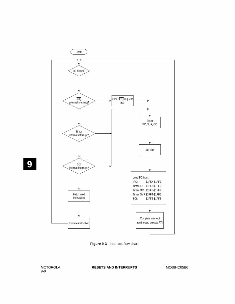
MOTOROLA9-8
MC68HC05B6RESETS AND INTERRUPTS
9
Figure 9-3 Interrupt flow chart
Reset
Is I-bit set?
IRQexternal interrupt?
Timerinternal interrupt?
SCIinternal interrupt?
Fetch nextinstruction
Execute instruction
Clear IRQ requestlatch
StackPC, X, A, CC
Set I-bit
Load PC from:IRQ: $1FFA-$1FFBTimer IC: $1FF8-$1FF9Timer OC: $1FF6-$1FF7Timer OVF:$1FF4-$1FF5SCI: $1FF2-$1FF3
Complete interruptroutine and execute RTI
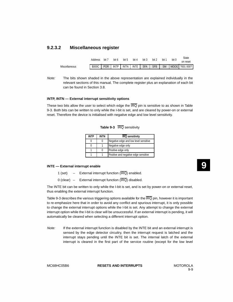
MC68HC05B6 MOTOROLA9-9
RESETS AND INTERRUPTS
9
9.2.3.2 Miscellaneous register
Note: The bits shown shaded in the above representation are explained individually in therelevant sections of this manual. The complete register plus an explanation of each bitcan be found in Section 3.8.
INTP, INTN — External interrupt sensitivity options
These two bits allow the user to select which edge the IRQ pin is sensitive to as shown in Table9-3. Both bits can be written to only while the I-bit is set, and are cleared by power-on or externalreset. Therefore the device is initialised with negative edge and low level sensitivity.
INTE — External interrupt enable
1 (set) – External interrupt function (IRQ) enabled.
0 (clear) – External interrupt function (IRQ) disabled.
The INTE bit can be written to only while the I-bit is set, and is set by power-on or external reset,thus enabling the external interrupt function.
Table 9-3 describes the various triggering options available for the IRQ pin, however it is importantto re-emphasize here that in order to avoid any conflict and spurious interrupt, it is only possibleto change the external interrupt options while the I-bit is set. Any attempt to change the externalinterrupt option while the I-bit is clear will be unsuccessful. If an external interrupt is pending, it willautomatically be cleared when selecting a different interrupt option.
Note: If the external interrupt function is disabled by the INTE bit and an external interrupt issensed by the edge detector circuitry, then the interrupt request is latched and theinterrupt stays pending until the INTE bit is set. The internal latch of the externalinterrupt is cleared in the first part of the service routine (except for the low level
Address bit 7 bit 6 bit 5 bit 4 bit 3 bit 2 bit 1 bit 0State
on reset
Miscellaneous $000C POR INTP INTN INTE SFA SFB SM WDOG ?001 000?
Table 9-3 IRQ sensitivity
INTP INTN IRQ sensitivity
0 0 Negative edge and low level sensitive
0 1 Negative edge only
1 0 Positive edge only
1 1 Positive and negative edge sensitive
MOTOROLA9-10
MC68HC05B6RESETS AND INTERRUPTS
9
interrupt which is not latched); therefore, only one external interrupt pulse can belatched during tILIL and serviced as soon as the I-bit is cleared.
9.2.3.3 Timer interrupts
There are five different timer interrupt flags (ICF1, ICF2, OCF1, OCF2 and TOF) that will cause atimer interrupt whenever they are set and enabled. These five interrupt flags are found in the fivemost significant bits of the timer status register (TSR) at location $0013. ICF1 and ICF2 will vectorto the service routine defined by $1FF8-$1FF9, OCF1 and OCF2 will vector to the service routinedefined by $1FF6–$1FF7 and TOF will vector to the service routine defined by $1FF4–$1FF5 asshown in Figure 5-1.
There are three corresponding enable bits; ICIE for ICF1 and ICF2, OCIE for OCF1 and OCF2,and TOIE for TOF. These enable bits are located in the timer control register (TCR) at address$0012. See Section 5.2.1 and Section 5.2.2 for further information.
9.2.3.4 Serial communications interface (SCI) interrupts
There are five different interrupt flags (TDRE, TC, OR, RDRF and IDLE) that cause SCI interruptswhenever they are set and enabled. These five interrupt flags are found in the five most significantbits of the SCI status register (SCSR) at location $0010.
There are four corresponding enable bits: TIE for TDRE, TCIE for TC, RIE for OR and RDRF, andILIE for IDLE. These enable bits are located in the serial communications control register 2(SCCR2) at address $000F. See Section 6.11.3 and Section 6.11.4.
The SCI interrupt causes the program counter to vector to the address pointed to by memorylocations $1FF2 and $1FF3 which contain the starting address of the interrupt service routine.Software in the SCI interrupt service routine must determine the priority and cause of the interruptby examining the interrupt flags and the status bits located in the serial communications statusregister SCSR (address $0010).
The general sequence for clearing an interrupt is a software sequence of accessing the serialcommunications status register while the flag is set followed by a read or write of an associatedregister. Refer to Section 6 for a description of the SCI system and its interrupts.
MC68HC05B6 MOTOROLA9-11
RESETS AND INTERRUPTS
9
9.2.4 Hardware controlled interrupt sequence
The following three functions: reset, STOP and WAIT, are not in the strictest sense interrupts. However,they are acted upon in a similar manner. Flowcharts for STOP and WAIT are shown in Figure 2-4.
RESET: A reset condition causes the program to vector to its starting address, which iscontained in memory locations $1FFE (MSB) and $1FFF (LSB). The I-bit in thecondition code register is also set, to disable interrupts.
STOP: The STOP instruction causes the oscillator to be turned off and the processor to ‘sleep’until an external interrupt (IRQ) or occurs or the device is reset.
WAIT: The WAIT instruction causes all processor clocks to stop, but leaves the timer clocksrunning. This ‘rest’ state of the processor can be cleared by reset, an external interrupt(IRQ), a timer interrupt or an SCI interrupt. There are no special WAIT vectors for theseindividual interrupts.

MOTOROLA9-12
MC68HC05B6RESETS AND INTERRUPTS
THIS PAGE INTENTIONALLY LEFT BLANK
9
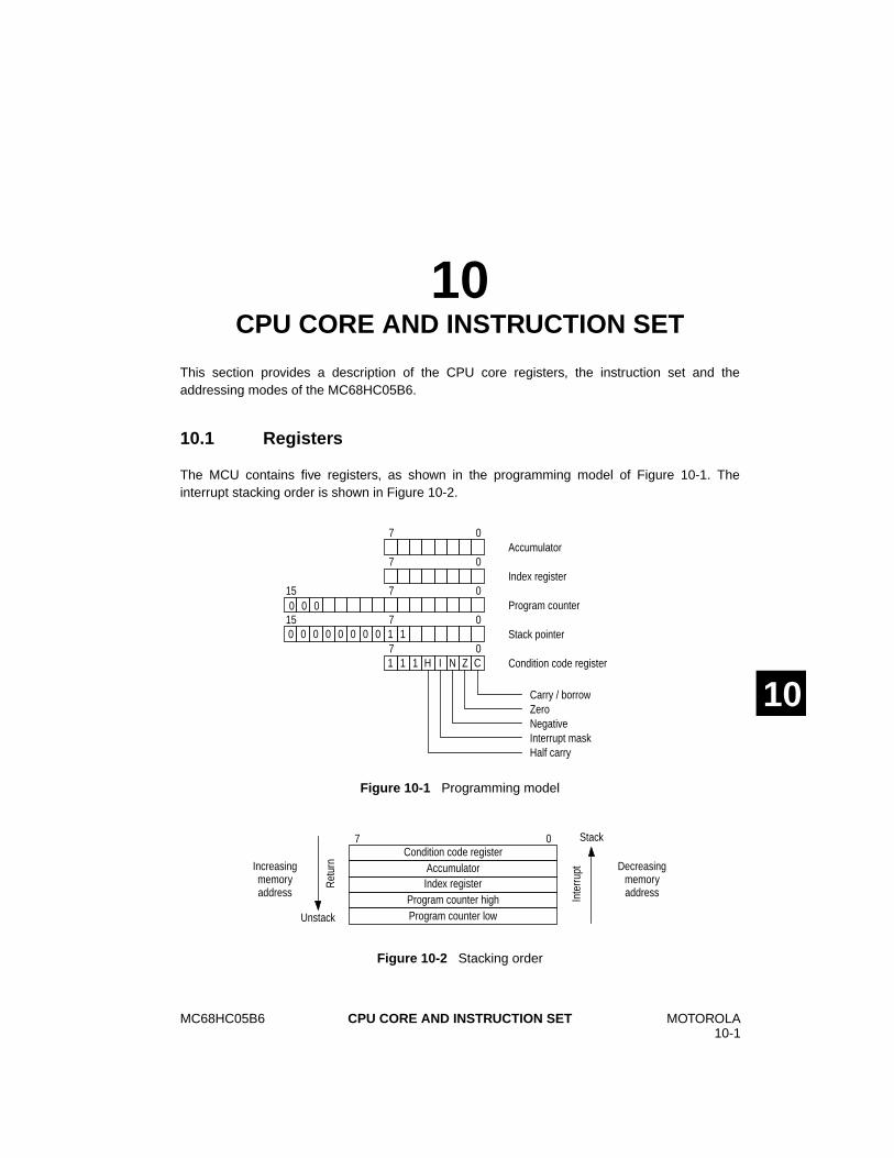
MC68HC05B6 MOTOROLA10-1
CPU CORE AND INSTRUCTION SET
10
10CPU CORE AND INSTRUCTION SET
This section provides a description of the CPU core registers, the instruction set and theaddressing modes of the MC68HC05B6.
10.1 Registers
The MCU contains five registers, as shown in the programming model of Figure 10-1. Theinterrupt stacking order is shown in Figure 10-2.
Figure 10-1 Programming model
Figure 10-2 Stacking order
Accumulator
Index register
Program counter
Stack pointer
Condition code register
Carry / borrowZeroNegativeInterrupt maskHalf carry
7 0
7 0
15 7 0
015 7 0
0 0 0 0 0 0 0 1 17 01 1 1 H I N Z C
000
Condition code registerAccumulatorIndex register
Program counter highProgram counter low
7 0 Stack
Unstack
Decreasingmemoryaddress
Increasingmemoryaddress In
terru
pt
Ret
urn
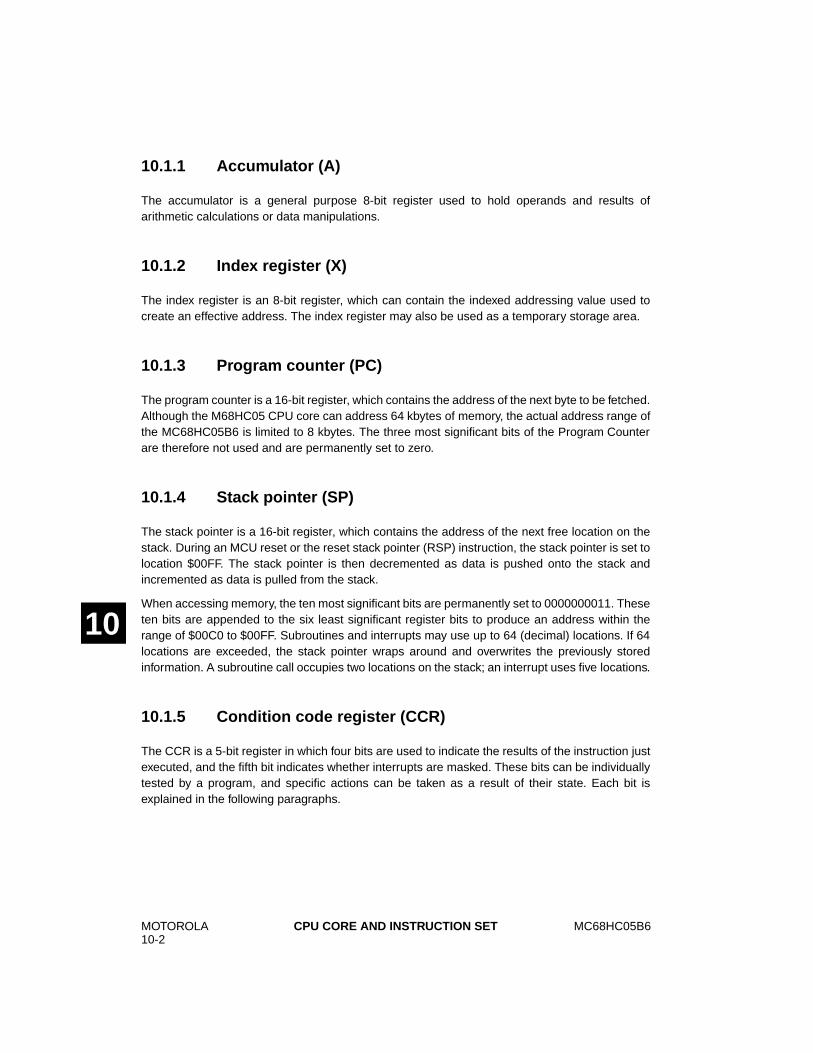
MOTOROLA10-2
MC68HC05B6CPU CORE AND INSTRUCTION SET
10
10.1.1 Accumulator (A)
The accumulator is a general purpose 8-bit register used to hold operands and results ofarithmetic calculations or data manipulations.
10.1.2 Index register (X)
The index register is an 8-bit register, which can contain the indexed addressing value used tocreate an effective address. The index register may also be used as a temporary storage area.
10.1.3 Program counter (PC)
The program counter is a 16-bit register, which contains the address of the next byte to be fetched.Although the M68HC05 CPU core can address 64 kbytes of memory, the actual address range ofthe MC68HC05B6 is limited to 8 kbytes. The three most significant bits of the Program Counterare therefore not used and are permanently set to zero.
10.1.4 Stack pointer (SP)
The stack pointer is a 16-bit register, which contains the address of the next free location on thestack. During an MCU reset or the reset stack pointer (RSP) instruction, the stack pointer is set tolocation $00FF. The stack pointer is then decremented as data is pushed onto the stack andincremented as data is pulled from the stack.
When accessing memory, the ten most significant bits are permanently set to 0000000011. Theseten bits are appended to the six least significant register bits to produce an address within therange of $00C0 to $00FF. Subroutines and interrupts may use up to 64 (decimal) locations. If 64locations are exceeded, the stack pointer wraps around and overwrites the previously storedinformation. A subroutine call occupies two locations on the stack; an interrupt uses five locations.
10.1.5 Condition code register (CCR)
The CCR is a 5-bit register in which four bits are used to indicate the results of the instruction justexecuted, and the fifth bit indicates whether interrupts are masked. These bits can be individuallytested by a program, and specific actions can be taken as a result of their state. Each bit isexplained in the following paragraphs.
MC68HC05B6 MOTOROLA10-3
CPU CORE AND INSTRUCTION SET
10
Half carry (H)
This bit is set during ADD and ADC operations to indicate that a carry occurred between bits 3 and 4.
Interrupt (I)
When this bit is set all maskable interrupts are masked. If an interrupt occurs while this bit is set,the interrupt is latched and remains pending until the interrupt bit is cleared.
Negative (N)
When set, this bit indicates that the result of the last arithmetic, logical, or data manipulation wasnegative.
Zero (Z)
When set, this bit indicates that the result of the last arithmetic, logical, or data manipulation was zero.
Carry/borrow (C)
When set, this bit indicates that a carry or borrow out of the arithmetic logical unit (ALU) occurredduring the last arithmetic operation. This bit is also affected during bit test and branch instructionsand during shifts and rotates.
10.2 Instruction set
The MCU has a set of 62 basic instructions. They can be grouped into five different types asfollows:
– Register/memory
– Read/modify/write
– Branch
– Bit manipulation
– Control
The following paragraphs briefly explain each type. All the instructions within a given type arepresented in individual tables.
This MCU uses all the instructions available in the M146805 CMOS family plus one more: theunsigned multiply (MUL) instruction. This instruction allows unsigned multiplication of the contentsof the accumulator (A) and the index register (X). The high-order product is then stored in theindex register and the low-order product is stored in the accumulator. A detailed definition of theMUL instruction is shown in Table 10-1.
MOTOROLA10-4
MC68HC05B6CPU CORE AND INSTRUCTION SET
10
10.2.1 Register/memory Instructions
Most of these instructions use two operands. The first operand is either the accumulator or theindex register. The second operand is obtained from memory using one of the addressing modes.The jump unconditional (JMP) and jump to subroutine (JSR) instructions have no registeroperand. Refer to Table 10-2 for a complete list of register/memory instructions.
10.2.2 Branch instructions
These instructions cause the program to branch if a particular condition is met; otherwise, nooperation is performed. Branch instructions are two-byte instructions. Refer to Table 10-3.
10.2.3 Bit manipulation instructions
The MCU can set or clear any writable bit that resides in the first 256 bytes of the memory space(page 0). All port data and data direction registers, timer and serial interface registers,control/status registers and a portion of the on-chip RAM reside in page 0. An additional featureallows the software to test and branch on the state of any bit within these locations. The bit set, bitclear, bit test and branch functions are all implemented with single instructions. For the test andbranch instructions, the value of the bit tested is also placed in the carry bit of the condition coderegister. Refer to Table 10-4.
10.2.4 Read/modify/write instructions
These instructions read a memory location or a register, modify or test its contents, and write themodified value back to memory or to the register. The test for negative or zero (TST) instruction isan exception to this sequence of reading, modifying and writing, since it does not modify the value.Refer to Table 10-5 for a complete list of read/modify/write instructions.
10.2.5 Control instructions
These instructions are register reference instructions and are used to control processor operationduring program execution. Refer to Table 10-6 for a complete list of control instructions.
10.2.6 Tables
Tables for all the instruction types listed above follow. In addition there is a complete alphabeticallisting of all the instructions (see Table 10-7 and Table 10-8), and an opcode map for the instructionset of the M68HC05 MCU family (see Table 10-9).
MC68HC05B6 MOTOROLA10-5
CPU CORE AND INSTRUCTION SET
10
Table 10-1 MUL instruction
Operation X:A ← X*A
DescriptionMultiplies the eight bits in the index register by the eightbits in the accumulator and places the 16-bit result in theconcatenated accumulator and index register.
Condition codes
H : ClearedI : Not affectedN : Not affectedZ : Not affectedC : Cleared
Source MUL
FormAddressing mode Cycles Bytes Opcode
Inherent 11 1 $42
Table 10-2 Register/memory instructions
Addressing modes
Immediate Direct ExtendedIndexed
(nooffset)
Indexed(8-bit
offset)
Indexed(16-bitoffset)
Function
Mne
mon
ic
Opc
ode
# By
tes
# Cy
cles
Opc
ode
# By
tes
# Cy
cles
Opc
ode
# By
tes
# Cy
cles
Opc
ode
# By
tes
# Cy
cles
Opc
ode
# By
tes
# Cy
cles
Opc
ode
# By
tes
# Cy
cles
Load A from memory LDA A6 2 2 B6 2 3 C6 3 4 F6 1 3 E6 2 4 D6 3 5
Load X from memory LDX AE 2 2 BE 2 3 CE 3 4 FE 1 3 EE 2 4 DE 3 5
Store A in memory STA B7 2 4 C7 3 5 F7 1 4 E7 2 5 D7 3 6
Store X in memory STX BF 2 4 CF 3 5 FF 1 4 EF 2 5 DF 3 6
Add memory to A ADD AB 2 2 BB 2 3 CB 3 4 FB 1 3 EB 2 4 DB 3 5
Add memory and carry to A ADC A9 2 2 B9 2 3 C9 3 4 F9 1 3 E9 2 4 D9 3 5
Subtract memory SUB A0 2 2 B0 2 3 C0 3 4 F0 1 3 E0 2 4 D0 3 5
Subtract memory from Awith borrow
SBC A2 2 2 B2 2 3 C2 3 4 F2 1 3 E2 2 4 D2 3 5
AND memory with A AND A4 2 2 B4 2 3 C4 3 4 F4 1 3 E4 2 4 D4 3 5
OR memory with A ORA AA 2 2 BA 2 3 CA 3 4 FA 1 3 EA 2 4 DA 3 5
Exclusive OR memory with A EOR A8 2 2 B8 2 3 C8 3 4 F8 1 3 E8 2 4 D8 3 5
Arithmetic compare Awith memory
CMP A1 2 2 B1 2 3 C1 3 4 F1 1 3 E1 2 4 D1 3 5
Arithmetic compare Xwith memory
CPX A3 2 2 B3 2 3 C3 3 4 F3 1 3 E3 2 4 D3 3 5
Bit test memory with A(logical compare)
BIT A5 2 2 B5 2 3 C5 3 4 F5 1 3 E5 2 4 D5 3 5
Jump unconditional JMP BC 2 2 CC 3 3 FC 1 2 EC 2 3 DC 3 4
Jump to subroutine JSR BD 2 5 CD 3 6 FD 1 5 ED 2 6 DD 3 7
MOTOROLA10-6
MC68HC05B6CPU CORE AND INSTRUCTION SET
10
Table 10-3 Branch instructions
Relative addressing mode
Function Mnemonic Opcode # Bytes # Cycles
Branch always BRA 20 2 3
Branch never BRN 21 2 3
Branch if higher BHI 22 2 3
Branch if lower or same BLS 23 2 3
Branch if carry clear BCC 24 2 3
(Branch if higher or same) (BHS) 24 2 3
Branch if carry set BCS 25 2 3
(Branch if lower) (BLO) 25 2 3
Branch if not equal BNE 26 2 3
Branch if equal BEQ 27 2 3
Branch if half carry clear BHCC 28 2 3
Branch if half carry set BHCS 29 2 3
Branch if plus BPL 2A 2 3
Branch if minus BMI 2B 2 3
Branch if interrupt mask bit is clear BMC 2C 2 3
Branch if interrupt mask bit is set BMS 2D 2 3
Branch if interrupt line is low BIL 2E 2 3
Branch if interrupt line is high BIH 2F 2 3
Branch to subroutine BSR AD 2 6
Table 10-4 Bit manipulation instructions
Addressing Modes
Bit set/clear Bit test and branch
Function Mnemonic Opcode # Bytes # Cycles Opcode # Bytes # Cycles
Branch if bit n is set BRSET n (n=0–7) 2•n 3 5
Branch if bit n is clear BRCLR n (n=0–7) 01+2•n 3 5
Set bit n BSET n (n=0–7) 10+2•n 2 5
Clear bit n BCLR n (n=0–7) 11+2•n 2 5
MC68HC05B6 MOTOROLA10-7
CPU CORE AND INSTRUCTION SET
10
Table 10-5 Read/modify/write instructions
Addressing modes
Inherent(A)
Inherent(X)
DirectIndexed
(nooffset)
Indexed(8-bit
offset)
Function
Mne
mon
ic
Opc
ode
# By
tes
# Cy
cles
Opc
ode
# By
tes
# Cy
cles
Opc
ode
# By
tes
# Cy
cles
Opc
ode
# By
tes
# Cy
cles
Opc
ode
# By
tes
# Cy
cles
Increment INC 4C 1 3 5C 1 3 3C 2 5 7C 1 5 6C 2 6
Decrement DEC 4A 1 3 5A 1 3 3A 2 5 7A 1 5 6A 2 6
Clear CLR 4F 1 3 5F 1 3 3F 2 5 7F 1 5 6F 2 6
Complement COM 43 1 3 53 1 3 33 2 5 73 1 5 63 2 6
Negate (two’s complement) NEG 40 1 3 50 1 3 30 2 5 70 1 5 60 2 6
Rotate left through carry ROL 49 1 3 59 1 3 39 2 5 79 1 5 69 2 6
Rotate right through carry ROR 46 1 3 56 1 3 36 2 5 76 1 5 66 2 6
Logical shift left LSL 48 1 3 58 1 3 38 2 5 78 1 5 68 2 6
Logical shift right LSR 44 1 3 54 1 3 34 2 5 74 1 5 64 2 6
Arithmetic shift right ASR 47 1 3 57 1 3 37 2 5 77 1 5 67 2 6
Test for negative or zero TST 4D 1 3 5D 1 3 3D 2 4 7D 1 4 6D 2 5
Multiply MUL 42 1 11
Table 10-6 Control instructions
Inherent addressing mode
Function Mnemonic Opcode # Bytes # Cycles
Transfer A to X TAX 97 1 2
Transfer X to A TXA 9F 1 2
Set carry bit SEC 99 1 2
Clear carry bit CLC 98 1 2
Set interrupt mask bit SEI 9B 1 2
Clear interrupt mask bit CLI 9A 1 2
Software interrupt SWI 83 1 10
Return from subroutine RTS 81 1 6
Return from interrupt RTI 80 1 9
Reset stack pointer RSP 9C 1 2
No-operation NOP 9D 1 2
Stop STOP 8E 1 2
Wait WAIT 8F 1 2
MOTOROLA10-8
MC68HC05B6CPU CORE AND INSTRUCTION SET
10
Table 10-7 Instruction set (1 of 2)
MnemonicAddressing modes Condition codes
INH IMM DIR EXT REL IX IX1 IX2 BSC BTB H I N Z C
ADC •
ADD •
AND • • •
ASL • •
ASR • •
BCC • • • • •
BCLR • • • • •
BCS • • • • •
BEQ • • • • •
BHCC • • • • •
BHCS • • • • •
BHI • • • • •
BHS • • • • •
BIH • • • • •
BIL • • • • •
BIT • • •
BLO • • • • •
BLS • • • • •
BMC • • • • •
BMI • • • • •
BMS • • • • •
BNE • • • • •
BPL • • • • •
BRA • • • • •
BRN • • • • •
BRCLR • • • •
BRSET • • • •
BSET • • • • •
BSR • • • • •
CLC • • • • 0
CLI • 0 • • •
CLR • • 0 1 •
CMP • •
Condition code symbols
H Half carry (from bit 3)Tested and set if true,cleared otherwise
I Interrupt mask • Not affected
N Negate (sign bit) ? Load CCR from stack
Z Zero 0 Cleared
C Carry/borrow 1 Set
Not implemented
Address mode abbreviationsBSC Bit set/clear IMM Immediate
BTB Bit test & branch IX Indexed (no offset)
DIR Direct IX1 Indexed, 1 byte offset
EXT Extended IX2 Indexed, 2 byte offset
INH Inherent REL Relative
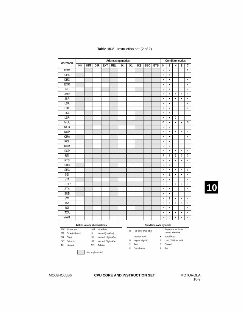
MC68HC05B6 MOTOROLA10-9
CPU CORE AND INSTRUCTION SET
10
Table 10-8 Instruction set (2 of 2)
MnemonicAddressing modes Condition codes
INH IMM DIR EXT REL IX IX1 IX2 BSC BTB H I N Z C
COM • • 1
CPX • •
DEC • • •
EOR • • •
INC • • •
JMP • • • • •
JSR • • • • •
LDA • • •
LDX • • •
LSL • •
LSR • • 0
MUL 0 • • • 0
NEG • •
NOP • • • • •
ORA • • •
ROL • •
ROR • •
RSP • • • • •
RTI ? ? ? ? ?
RTS • • • • •
SBC • •
SEC • • • • 1
SEI • 1 • • •
STA • • •
STOP • 0 • • •
STX • • •
SUB • •
SWI • 1 • • •
TAX • • • • •
TST • • •
TXA • • • • •
WAIT • 0 • • •
Condition code symbols
H Half carry (from bit 3)Tested and set if true,cleared otherwise
I Interrupt mask • Not affected
N Negate (sign bit) ? Load CCR from stack
Z Zero 0 Cleared
C Carry/borrow 1 Set
Not implemented
Address mode abbreviationsBSC Bit set/clear IMM Immediate
BTB Bit test & branch IX Indexed (no offset)
DIR Direct IX1 Indexed, 1 byte offset
EXT Extended IX2 Indexed, 2 byte offset
INH Inherent REL Relative
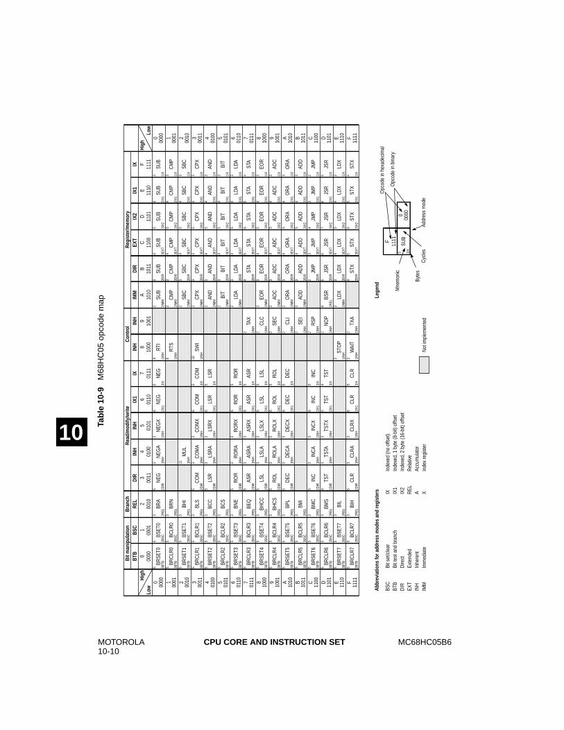
MOTOROLA10-10
MC68HC05B6CPU CORE AND INSTRUCTION SET
10 Tabl
e 10
-9M
68H
C05
opc
ode
map
Bit m
anip
ulat
ion
Bran
chRe
ad/m
odify
/writ
eCo
ntro
lRe
gist
er/m
emor
yBT
BBS
CRE
LDI
RIN
HIN
HIX
1IX
INH
INH
IMM
DIR
EXT
IX2
IX1
IXHi
gh0
12
34
56
78
9A
BC
DE
FHi
ghLo
w00
0000
0100
1000
1101
0001
0101
1001
1110
0010
0110
1010
1111
0011
0111
1011
11Lo
w0
0000
55
35
33
65
92
34
54
30
0000
BRSE
T0BS
ET0
BRA
NEG
NEG
AN
EGX
NEG
NEG
RTI
SUB
SUB
SUB
SUB
SUB
SUB
3BTB
2BSC
2REL
2DIR
1IN
H1I
NH
2IX1
1IX
1IN
H2I
MM
2DIR
3EXT
3IX2
2IX1
1IX
100
015
53
62
34
54
31
0001
BRC
LR0
BCLR
0BR
NRT
SC
MP
CM
PC
MP
CM
PC
MP
CM
P3B
TB2B
SC2R
EL1I
NH
2IM
M2D
IR3E
XT3I
X22I
X11I
X
200
105
53
112
34
54
32
0010
BRSE
T1BS
ET1
BHI
MU
LSB
CSB
CSB
CSB
CSB
CSB
C3B
TB2B
SC2R
EL1I
NH
2IM
M2D
IR3E
XT3I
X22I
X11I
X
300
115
53
53
36
510
23
45
43
300
11BR
CLR
1BC
LR1
BLS
CO
MC
OM
AC
OM
XC
OM
CO
MSW
IC
PXC
PXC
PXC
PXC
PXC
PX3B
TB2B
SC2R
EL2D
IR1I
NH
1IN
H2I
X11I
X1I
NH
2IM
M2D
IR3E
XT3I
X22I
X11I
X
401
005
53
53
36
52
34
54
34
0100
BRSE
T2BS
ET2
BCC
LSR
LSR
ALS
RX
LSR
LSR
AND
AND
AND
AND
AND
AND
3BTB
2BSC
2REL
2DIR
1IN
H1I
NH
2IX1
1IX
2IM
M2D
IR3E
XT3I
X22I
X11I
X
501
015
53
23
45
43
501
01BR
CLR
2BC
LR2
BCS
BIT
BIT
BIT
BIT
BIT
BIT
3BTB
2BSC
2REL
2IM
M2D
IR3E
XT3I
X22I
X11I
X
601
105
53
53
36
52
34
54
36
0110
BRSE
T3BS
ET3
BNE
RO
RRO
RA
ROR
XR
OR
ROR
LDA
LDA
LDA
LDA
LDA
LDA
3BTB
2BSC
2REL
2DIR
1IN
H1I
NH
2IX1
1IX
2IM
M2D
IR3E
XT3I
X22I
X11I
X
701
115
53
53
36
52
45
65
47
0111
BRC
LR3
BCLR
3BE
QAS
RAS
RA
ASR
XAS
RAS
RTA
XST
AST
AST
AST
AST
A3B
TB2B
SC2R
EL2D
IR1I
NH
1IN
H2I
X11I
X1I
NH
2DIR
3EXT
3IX2
2IX1
1IX
810
005
53
53
36
52
23
45
43
810
00BR
SET4
BSET
4BH
CC
LSL
LSLA
LSLX
LSL
LSL
CLC
EOR
EOR
EOR
EOR
EOR
EOR
3BTB
2BSC
2REL
2DIR
1IN
H1I
NH
2IX1
1IX
1IN
H2I
MM
2DIR
3EXT
3IX2
2IX1
1IX
910
015
53
53
36
52
23
45
43
910
01BR
CLR
4BC
LR4
BHC
SRO
LRO
LARO
LXRO
LRO
LSE
CAD
CAD
CAD
CAD
CAD
CAD
C3B
TB2B
SC2R
EL2D
IR1I
NH
1IN
H2I
X11I
X1I
NH
2IM
M2D
IR3E
XT3I
X22I
X11I
X
A10
105
53
53
36
52
23
45
43
A10
10BR
SET5
BSET
5BP
LD
ECD
ECA
DEC
XD
ECD
ECC
LIO
RA
OR
AO
RA
OR
AO
RA
OR
A3B
TB2B
SC2R
EL2D
IR1I
NH
1IN
H2I
X11I
X1I
NH
2IM
M2D
IR3E
XT3I
X22I
X11I
X
B10
115
53
22
34
54
3B
1011
BRC
LR5
BCLR
5BM
ISE
IAD
DAD
DAD
DAD
DAD
DAD
D3B
TB2B
SC2R
EL1I
NH
2IM
M2D
IR3E
XT3I
X22I
X11I
X
C11
005
53
53
36
52
23
43
2C
1100
BRSE
T6BS
ET6
BMC
INC
INC
AIN
CX
INC
INC
RSP
JMP
JMP
JMP
JMP
JMP
3BTB
2BSC
2REL
2DIR
1IN
H1I
NH
2IX1
1IX
1IN
H2D
IR3E
XT3I
X22I
X11I
X
D11
015
53
43
35
42
65
67
65
D11
01BR
CLR
6BC
LR6
BMS
TST
TSTA
TSTX
TST
TST
NO
PBS
RJS
RJS
RJS
RJS
RJS
R3B
TB2B
SC2R
EL2D
IR1I
NH
1IN
H2I
X11I
X1I
NH
2REL
2DIR
3EXT
3IX2
2IX1
1IX
E11
105
53
22
34
54
3E
1110
BRSE
T7BS
ET7
BIL
STO
PLD
XLD
XLD
XLD
XLD
XLD
X3B
TB2B
SC2R
EL1I
NH
2IM
M2D
IR3E
XT3I
X22I
X11I
X
F11
115
53
53
36
52
24
56
54
F11
11BR
CLR
7BC
LR7
BIH
CLR
CLR
AC
LRX
CLR
CLR
WAI
TTX
AST
XST
XST
XST
XST
X3B
TB2B
SC2R
EL2D
IR1I
NH
1IN
H2I
X11I
X1I
NH
1IN
H2D
IR3E
XT3I
X22I
X11I
X
F11
113
000
00SU
B1I
X
Opc
ode
in h
exad
ecim
al
Opc
ode
in b
inar
y
Addr
ess
mod
eC
ycle
sBy
tes
Mne
mon
ic
Lege
ndAb
brev
iatio
ns fo
r add
ress
mod
es a
nd re
gist
ers
BSC
BTB
DIR
EXT
INH
IMM
IX IX1
IX2
REL
A X
Bit s
et/c
lear
Bit t
est a
nd b
ranc
hD
irect
Exte
nded
Inhe
rent
Imm
edia
te
Inde
xed
(no
offs
et)
Inde
xed,
1 b
yte
(8-b
it) o
ffset
Inde
xed,
2 b
yte
(16-
bit)
offs
etR
elat
iveAc
cum
ulat
orIn
dex
regi
ster
Not
impl
emen
ted
MC68HC05B6 MOTOROLA10-11
CPU CORE AND INSTRUCTION SET
10
10.3 Addressing modes
Ten different addressing modes provide programmers with the flexibility to optimize their code forall situations. The various indexed addressing modes make it possible to locate data tables, codeconversion tables and scaling tables anywhere in the memory space. Short indexed accesses aresingle byte instructions; the longest instructions (three bytes) enable access to tables throughoutmemory. Short absolute (direct) and long absolute (extended) addressing are also included. Oneor two byte direct addressing instructions access all data bytes in most applications. Extendedaddressing permits jump instructions to reach all memory locations.
The term ‘effective address’ (EA) is used in describing the various addressing modes. Theeffective address is defined as the address from which the argument for an instruction is fetchedor stored. The ten addressing modes of the processor are described below. Parentheses are usedto indicate ‘contents of’ the location or register referred to. For example, (PC) indicates thecontents of the location pointed to by the PC (program counter). An arrow indicates ‘is replacedby’ and a colon indicates concatenation of two bytes. For additional details and graphicalillustrations, refer to the M6805 HMOS/M146805 CMOS Famil y Micr ocomputer/Microprocessor User's Manual or to the M68HC05 Applications Guide .
10.3.1 Inherent
In the inherent addressing mode, all the information necessary to execute the instruction iscontained in the opcode. Operations specifying only the index register or accumulator, as well asthe control instruction, with no other arguments are included in this mode. These instructions areone byte long.
10.3.2 Immediate
In the immediate addressing mode, the operand is contained in the byte immediately following theopcode. The immediate addressing mode is used to access constants that do not change duringprogram execution (e.g. a constant used to initialize a loop counter).
EA = PC+1; PC ← PC+2
10.3.3 Direct
In the direct addressing mode, the effective address of the argument is contained in a single bytefollowing the opcode byte. Direct addressing allows the user to directly address the lowest 256bytes in memory with a single two-byte instruction.
EA = (PC+1); PC ← PC+2Address bus high ← 0; Address bus low ← (PC+1)
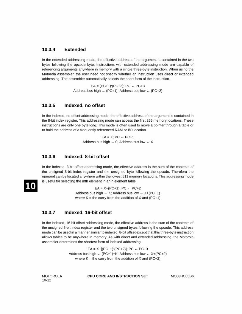
MOTOROLA10-12
MC68HC05B6CPU CORE AND INSTRUCTION SET
10
10.3.4 Extended
In the extended addressing mode, the effective address of the argument is contained in the twobytes following the opcode byte. Instructions with extended addressing mode are capable ofreferencing arguments anywhere in memory with a single three-byte instruction. When using theMotorola assembler, the user need not specify whether an instruction uses direct or extendedaddressing. The assembler automatically selects the short form of the instruction.
EA = (PC+1):(PC+2); PC ← PC+3Address bus high ← (PC+1); Address bus low ← (PC+2)
10.3.5 Indexed, no offset
In the indexed, no offset addressing mode, the effective address of the argument is contained inthe 8-bit index register. This addressing mode can access the first 256 memory locations. Theseinstructions are only one byte long. This mode is often used to move a pointer through a table orto hold the address of a frequently referenced RAM or I/O location.
EA = X; PC ← PC+1Address bus high ← 0; Address bus low ← X
10.3.6 Indexed, 8-bit offset
In the indexed, 8-bit offset addressing mode, the effective address is the sum of the contents ofthe unsigned 8-bit index register and the unsigned byte following the opcode. Therefore theoperand can be located anywhere within the lowest 511 memory locations. This addressing modeis useful for selecting the mth element in an n element table.
EA = X+(PC+1); PC ← PC+2Address bus high ← K; Address bus low ← X+(PC+1)where K = the carry from the addition of X and (PC+1)
10.3.7 Indexed, 16-bit offset
In the indexed, 16-bit offset addressing mode, the effective address is the sum of the contents ofthe unsigned 8-bit index register and the two unsigned bytes following the opcode. This addressmode can be used in a manner similar to indexed, 8-bit offset except that this three-byte instructionallows tables to be anywhere in memory. As with direct and extended addressing, the Motorolaassembler determines the shortest form of indexed addressing.
EA = X+[(PC+1):(PC+2)]; PC ← PC+3Address bus high ← (PC+1)+K; Address bus low ← X+(PC+2)
where K = the carry from the addition of X and (PC+2)
MC68HC05B6 MOTOROLA10-13
CPU CORE AND INSTRUCTION SET
10
10.3.8 Relative
The relative addressing mode is only used in branch instructions. In relative addressing, thecontents of the 8-bit signed byte (the offset) following the opcode are added to the PC if, and onlyif, the branch conditions are true. Otherwise, control proceeds to the next instruction. The span ofrelative addressing is from –126 to +129 from the opcode address. The programmer need notcalculate the offset when using the Motorola assembler, since it calculates the proper offset andchecks to see that it is within the span of the branch.
EA = PC+2+(PC+1); PC ← EA if branch taken;otherwise EA = PC ← PC+2
10.3.9 Bit set/clear
In the bit set/clear addressing mode, the bit to be set or cleared is part of the opcode. The bytefollowing the opcode specifies the address of the byte in which the specified bit is to be set orcleared. Any read/write bit in the first 256 locations of memory, including I/O, can be selectivelyset or cleared with a single two-byte instruction.
EA = (PC+1); PC ← PC+2Address bus high ← 0; Address bus low ← (PC+1)
10.3.10 Bit test and branch
The bit test and branch addressing mode is a combination of direct addressing and relativeaddressing. The bit to be tested and its condition (set or clear) is included in the opcode. Theaddress of the byte to be tested is in the single byte immediately following the opcode byte (EA1).The signed relative 8-bit offset in the third byte (EA2) is added to the PC if the specified bit is setor cleared in the specified memory location. This single three-byte instruction allows the programto branch based on the condition of any readable bit in the first 256 locations of memory. The spanof branch is from –125 to +130 from the opcode address. The state of the tested bit is alsotransferred to the carry bit of the condition code register.
EA1 = (PC+1); PC ← PC+2Address bus high ← 0; Address bus low ← (PC+1)EA2 = PC+3+(PC+2); PC ← EA2 if branch taken;
otherwise PC ← PC+3

MOTOROLA10-14
MC68HC05B6CPU CORE AND INSTRUCTION SET
THIS PAGE INTENTIONALLY LEFT BLANK
10
MC68HC05B6 MOTOROLA11-1
ELECTRICAL SPECIFICATIONS
11
11ELECTRICAL SPECIFICATIONS
This section contains the electrical specifications and associated timing information for theMC68HC05B6.
11.1 Maximum ratings
Note: This device contains circuitry designed to protect against damage due to highelectrostatic voltages or electric fields. However, it is recommended that normalprecautions be taken to avoid the application of any voltages higher than those givenin the maximum ratings table to this high impedance circuit. For maximum reliability allunused inputs should be tied to either VSS or VDD.
(1) All voltages are with respect to VSS.
(2) Maximum current drain per pin is for one pin at a time, limited by an external resistor.
Table 11-1 Maximum ratings
Rating Symbol Value Unit
Supply voltage(1) VDD – 0.5 to +7.0 V
Input voltage VIN VSS – 0.5 to VDD + 0.5 V
Input voltage– Self-check mode (IRQ pin only)
VIN VSS – 0.5 to 2VDD + 0.5 V
Operating temperature range– Standard (MC68HC05B6)– Extended (MC68HC05B6C)– Automotive (MC68HC05B6M)
TA TL to TH0 to +70
–40 to +85–40 to +125
¡C
Storage temperature range TSTG – 65 to +150 ¡C
Current drain per pin (excluding VDD and VSS)(2)
– Source– Sink
IDIS
2545
mAmA
MOTOROLA11-2
MC68HC05B6ELECTRICAL SPECIFICATIONS
11
11.2 Thermal characteristics and power considerations
The average chip junction temperature, TJ, in degrees Celsius can be obtained from the following
equation:
[1]
where:
TA = Ambient temperature (¡C)
θJA = Package thermal resistance, junction-to-ambient (¡C/W)
PD = PINT + PI/O (W)
PINT = Internal chip power = IDD • VDD (W)
PI/O = Power dissipation on input and output pins (user determined)
An approximate relationship between PD and TJ (if PI/O is neglected) is:
[2]
Solving equations [1] and [2] for K gives:
[3]
where K is a constant for a particular part. K can be determined by measuring PD (at equilibrium)for a known TA. Using this value of K, the values of PD and TJ can be obtained for any value of TAby solving the above equations. The package thermal characteristics are shown in Table 11-2.
Table 11-2 Package thermal characteristics
Characteristics Symbol Value Unit
Thermal resistance
– 64-pin quad flat package θJA 50 ¡C/W
– Plastic 56 pin shrink DIL package θJA 50 ¡C/W
– Plastic 52 pin PLCC package θJA 50 ¡C/W
Figure 11-1 Equivalent test load
TJ TA PD θJA•( )+=
PDK
TJ 273+---------------------=
K PD TA 273+( )• θJA PD2•+=
Voltage Pins R1 R2 C
4.5V PA0–7, PB0–7, PC0–7 3.26k½ 2.38k½ 50pF
3.0V PA0–7, PB0–7, PC0–7 10.91k½ 6.32k½ 50pF
VDD = 4.5/3.0V
R2
R1C
Testpoint
MC68HC05B6 MOTOROLA11-3
ELECTRICAL SPECIFICATIONS
11
11.3 DC electrical characteristics
(1) All IDD measurements taken with suitable decoupling capacitors across the power supply to suppress the transientswitching currents inherent in CMOS designs (see Section 2).
(2) Typical values are at mid point of voltage range and at 25¡C only.
(3) RUN and WAIT IDD: measured using an external square-wave clock source (fOSC = 4.2MHz); all inputs 0.2 V fromrail; no DC loads; maximum load on outputs 50pF (20pF on OSC2).STOP /WAIT IDD: all ports configured as inputs; VIL = 0.2 V and VIH = VDD – 0.2 V: STOP IDD measured withOSC1 = VDD.WAIT IDD is affected linearly by the OSC2 capacitance.
Table 11-3 DC electrical characteristics for 5V operation
(VDD = 5 Vdc ± 10%, VSS = 0 Vdc, TA = TL to TH)Characteristic (1) Symbol Min Typ (2) Max Unit
Output voltageILOAD = – 10 µAILOAD = +10 µA
VOHVOL
VDD – 0.1—
——
—0.1
V
Output high voltage (ILOAD = 0.8mA)PA0–7, PB0–7, PC0–7, TCMP1, TCMP2
Output high voltage (ILOAD = 1.6mA)TDO, SCLK, PLMA, PLMB
VOH
VOH
VDD – 0.8
VDD – 0.8
VDD – 0.4
VDD – 0.4
—
—
V
Output low voltage (ILOAD = 1.6mA)PA0–7, PB0–7, PC0–7, TCMP1, TCMP2,
TDO, SCLK, PLMA, PLMBOutput low voltage (ILOAD = 1.6mA)
RESET
VOL
VOL
— 0.1
0.4
0.4
1
V
Input high voltagePA0–7, PB0–7, PC0–7, PD0–7, OSC1,IRQ, RESET, TCAP1, TCAP2, RDI
VIH 0.7VDD — VDD V
Input low voltagePA0–7, PB0–7, PC0–7, OSC1, IRQ, RESET,TCAP1, TCAP2, RDI
VIL VSS — 0.2VDD V
Supply current(3)
RUN (SM = 0) (See Figure 11-2)RUN (SM = 1) (See Figure 11-3)WAIT (SM = 0) (See Figure 11-4)WAIT (SM = 1) (See Figure 11-5)STOP
0 to 70 (standard)– 40 to 85 (extended)– 40 to 105 (extended)– 40 to 125 (automotive)
IDD
————
————
3.50.51
0.35
2———
61.521
10206060
mAmAmAmA
µAµAµAµA
High-Z leakage currentPA0–7, PB0–7, PC0–7, TDO, RESET, SCLK IIL — ±0.2 ±1 µA
Input current (0 to 70)IRQ, OSC1, TCAP1, TCAP2, RDI,PD0/AN0-PD7/AN7 (channel not selected)
IIN — ±0.2±0.2
±1±1
µA
Input current (– 40 to 125)IRQ, OSC1, TCAP1, TCAP2, RDI, IIN — — ±5 µA
CapacitancePorts (as input or output), RESET, TDO, SCLKIRQ, TCAP1, TCAP2, OSC1, RDIPD0/AN0–PD7/AN7 (A/D off)PD0/AN0–PD7/AN7 (A/D on)
COUTCINCINCIN
————
——1222
128
TBDTBD
pFpFpFpF
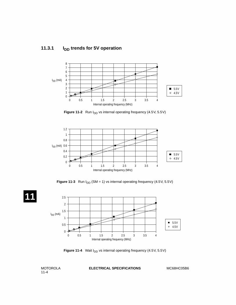
MOTOROLA11-4
MC68HC05B6ELECTRICAL SPECIFICATIONS
11
11.3.1 IDD trends for 5V operation
Figure 11-2 Run IDD vs internal operating frequency (4.5V, 5.5V)
Figure 11-3 Run IDD (SM = 1) vs internal operating frequency (4.5V, 5.5V)
Figure 11-4 Wait IDD vs internal operating frequency (4.5V, 5.5V)
876543210
0 0.5 1 1.5 2 2.5 3 3.5 4
IDD (mA)
Internal operating frequency (MHz)
5.5V4.5V
1.2
00 0.5 1 1.5 2 2.5 3 3.5 4
IDD (mA)
Internal operating frequency (MHz)
5.5V4.5V
1
0.8
0.6
0.4
0.2
2.5
00 0.5 1 1.5 2 2.5 3 3.5 4
IDD (mA)
Internal operating frequency (MHz)
5.5V4.5V
2
1.5
1
0.5
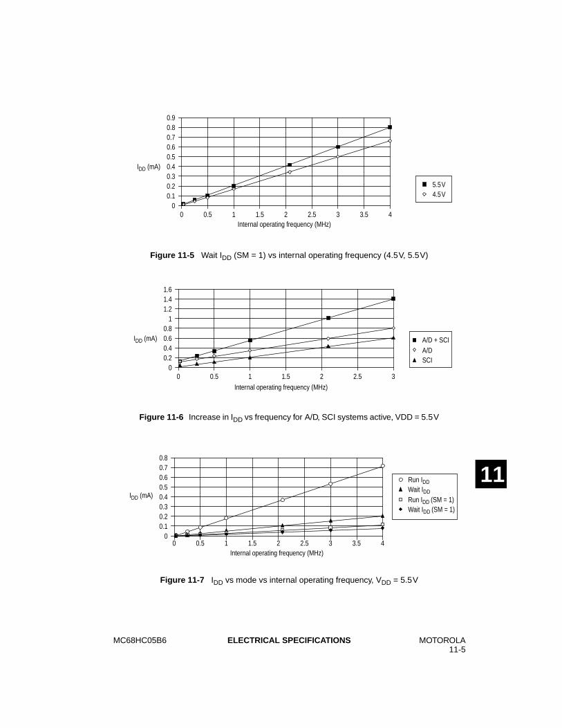
MC68HC05B6 MOTOROLA11-5
ELECTRICAL SPECIFICATIONS
11
Figure 11-5 Wait IDD (SM = 1) vs internal operating frequency (4.5V, 5.5V)
Figure 11-6 Increase in IDD vs frequency for A/D, SCI systems active, VDD = 5.5V
Figure 11-7 IDD vs mode vs internal operating frequency, VDD = 5.5V
0.80.70.60.50.40.30.20.1
00 0.5 1 1.5 2 2.5 3 3.5 4
IDD (mA)
Internal operating frequency (MHz)
5.5V4.5V
0.9
1.41.2
10.80.60.40.2
00 0.5 1 1.5 2 2.5 3
IDD (mA)
Internal operating frequency (MHz)
A/D + SCIA/D
1.6
SCI
0.80.70.60.50.40.30.20.1
00 0.5 1 1.5 2 2.5 3 3.5 4
IDD (mA)
Internal operating frequency (MHz)
Wait IDD (SM = 1)
Run IDDWait IDDRun IDD (SM = 1)
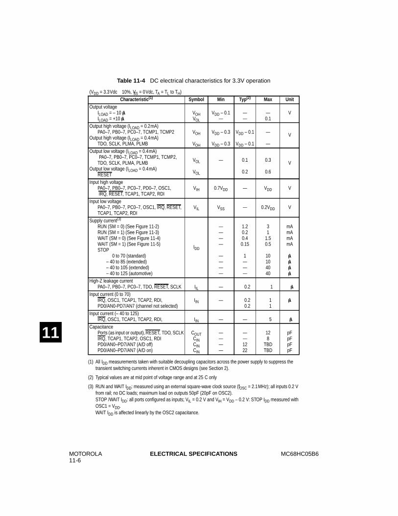
MOTOROLA11-6
MC68HC05B6ELECTRICAL SPECIFICATIONS
11
(1) All IDD measurements taken with suitable decoupling capacitors across the power supply to suppress thetransient switching currents inherent in CMOS designs (see Section 2).
(2) Typical values are at mid point of voltage range and at 25¡C only.
(3) RUN and WAIT IDD: measured using an external square-wave clock source (fOSC = 2.1MHz); all inputs 0.2 Vfrom rail; no DC loads; maximum load on outputs 50pF (20pF on OSC2).STOP /WAIT IDD: all ports configured as inputs; VIL = 0.2 V and VIH = VDD – 0.2 V: STOP IDD measured withOSC1 = VDD.WAIT IDD is affected linearly by the OSC2 capacitance.
Table 11-4 DC electrical characteristics for 3.3V operation
(VDD = 3.3Vdc ± 10%, VSS = 0Vdc, TA = TL to TH)Characteristic (1) Symbol Min Typ (2) Max Unit
Output voltageILOAD = – 10 µAILOAD = +10 µA
VOHVOL
VDD – 0.1—
——
—0.1
V
Output high voltage (ILOAD = 0.2mA)PA0–7, PB0–7, PC0–7, TCMP1, TCMP2
Output high voltage (ILOAD = 0.4mA)TDO, SCLK, PLMA, PLMB
VOH
VOH
VDD – 0.3
VDD – 0.3
VDD – 0.1
VDD – 0.1
—
—
V
Output low voltage (ILOAD = 0.4mA)PA0–7, PB0–7, PC0–7, TCMP1, TCMP2,
TDO, SCLK, PLMA, PLMBOutput low voltage (ILOAD = 0.4mA)
RESET
VOL
VOL
— 0.1
0.2
0.3
0.6
V
Input high voltagePA0–7, PB0–7, PC0–7, PD0–7, OSC1,IRQ, RESET, TCAP1, TCAP2, RDI
VIH 0.7VDD — VDD V
Input low voltagePA0–7, PB0–7, PC0–7, OSC1, IRQ, RESET,TCAP1, TCAP2, RDI
VIL VSS — 0.2VDD V
Supply current(3)
RUN (SM = 0) (See Figure 11-2)RUN (SM = 1) (See Figure 11-3)WAIT (SM = 0) (See Figure 11-4)WAIT (SM = 1) (See Figure 11-5)STOP
0 to 70 (standard)– 40 to 85 (extended)– 40 to 105 (extended)– 40 to 125 (automotive)
IDD
————
————
1.20.20.40.15
1———
31
1.50.5
10104040
mAmAmAmA
µAµAµAµA
High-Z leakage currentPA0–7, PB0–7, PC0–7, TDO, RESET, SCLK IIL — ±0.2 ±1 µA
Input current (0 to 70)IRQ, OSC1, TCAP1, TCAP2, RDI,PD0/AN0-PD7/AN7 (channel not selected)
IIN — ±0.2±0.2
±1±1
µA
Input current (– 40 to 125)IRQ, OSC1, TCAP1, TCAP2, RDI, IIN — — ±5 µA
CapacitancePorts (as input or output), RESET, TDO, SCLKIRQ, TCAP1, TCAP2, OSC1, RDIPD0/AN0–PD7/AN7 (A/D off)PD0/AN0–PD7/AN7 (A/D on)
COUTCINCINCIN
————
——1222
128
TBDTBD
pFpFpFpF
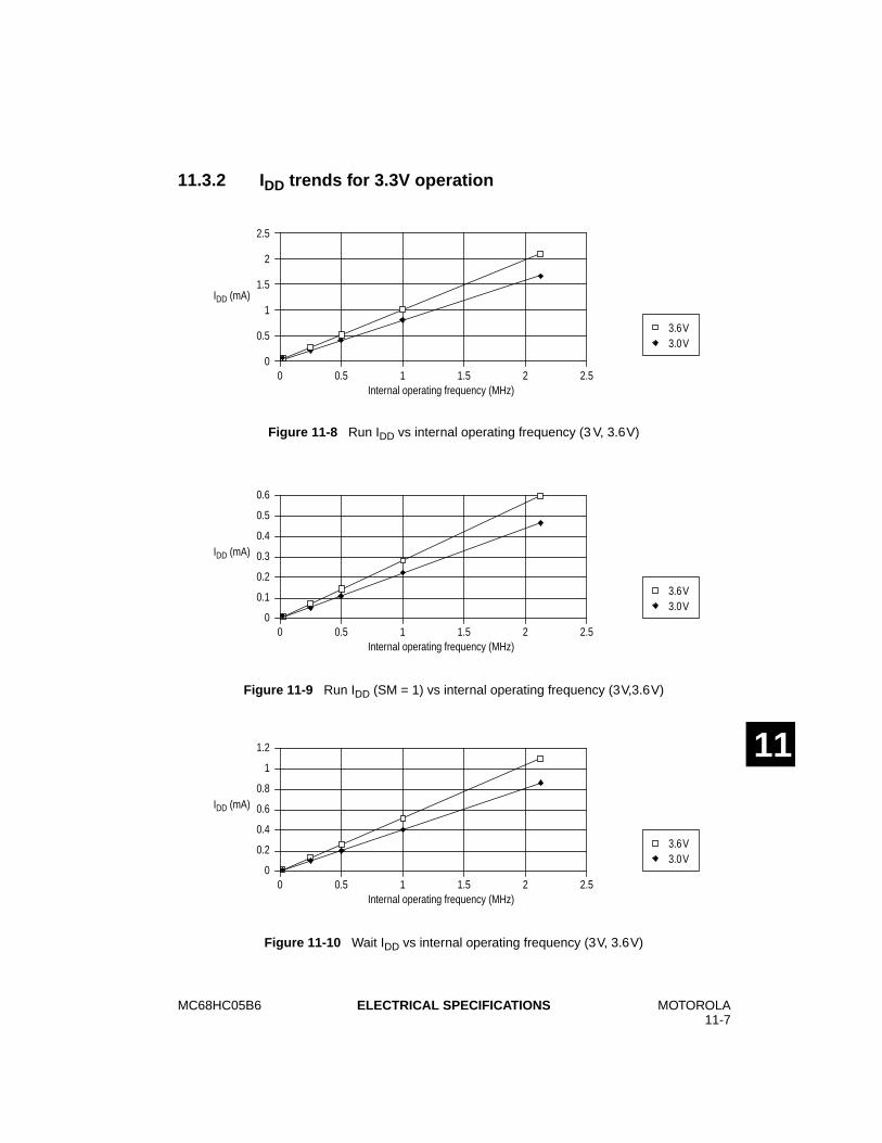
MC68HC05B6 MOTOROLA11-7
ELECTRICAL SPECIFICATIONS
11
11.3.2 IDD trends for 3.3V operation
Figure 11-8 Run IDD vs internal operating frequency (3 V, 3.6V)
Figure 11-9 Run IDD (SM = 1) vs internal operating frequency (3V,3.6V)
Figure 11-10 Wait IDD vs internal operating frequency (3V, 3.6V)
2.5
00 0.5 1 1.5 2 2.5
IDD (mA)
Internal operating frequency (MHz)
3.6V3.0V
2
1.5
1
0.5
0.6
00 0.5 1 1.5 2 2.5
IDD (mA)
Internal operating frequency (MHz)
3.6V3.0V
0.5
0.4
0.3
0.2
0.1
1.2
00 0.5 1 1.5 2 2.5
IDD (mA)
Internal operating frequency (MHz)
3.6V3.0V
1
0.8
0.6
0.4
0.2
MOTOROLA11-8
MC68HC05B6ELECTRICAL SPECIFICATIONS
11
Figure 11-11 Wait IDD (SM = 1) vs internal operating frequency (3V, 3.6V)
Figure 11-12 Increase in IDD vs frequency for A/D, SCI systems active, VDD = 3.6V
Figure 11-13 IDD vs mode vs internal operating frequency, VDD = 3.6V
0.5
00 0.5 1 1.5 2 2.5
IDD (mA)
Internal operating frequency (MHz)
3.6V3.0V
0.4
0.3
0.2
0.1
0.70.60.50.40.30.20.1
00 0.5 1 1.5 2 2.5
IDD (mA)
Internal operating frequency (MHz)
A/D
SCI
A/D + SCI
2.5
2
1.5
1
0.5
00 0.5 1 1.5 2 2.5
IDD (mA)
Internal operating frequency (MHz)
Run IDD
Wait IDD
Run IDD (SM=1)
Wait IDD (SM=1)
MC68HC05B6 MOTOROLA11-9
ELECTRICAL SPECIFICATIONS
11
11.4 A/D converter characteristics
(1) Performance verified down to 2.5V ÆVR, but accuracy is tested and guaranteed at ÆVR = 5V±10%.
(2) Source impedances greater than 10k½ will adversely affect internal charging time during input sampling.
(3) The external system error caused by input leakage current is approximately equal to the product of R source and inputcurrent. Input current to A/D channel will be dependent on external source impedance (see Figure 8-2).
Table 11-5 A/D characteristics for 5V operation
(VDD = 5.0 Vdc ± 10%, VSS = 0 Vdc, TA = TL to TH)
Characteristic Parameter Min Max Unit
Resolution Number of bits resolved by the A/D 8 — Bit
Non-linearity Max deviation from the best straight line through the A/Dtransfer characteristics(VRH = VDD and VRL = 0V)
— ± 0.5 LSB
Quantization error Uncertainty due to converter resolution — ± 0.5 LSB
Absolute accuracy Difference between the actual input voltage and thefull-scale equivalent of the binary code output code for allerrors
— ± 1 LSB
Conversion range Analog input voltage range VRL VRH V
VRH Maximum analog reference voltage VRL VDD + 0.1 V
VRL Minimum analog reference voltage VSS – 0.1 VRH V
ÆVR(1) Minimum difference between VRH and VRL 3 — V
Conversion time Total time to perform a single analog to digital conversiona. External clock (OSC1, OSC2)b. Internal RC oscillator
——
3232
tCYCµs
Monotonicity Conversion result never decreases with an increase ininput voltage and has no missing codes
GUARANTEED
Zero input reading Conversion result when VIN = VRL 00 — Hex
Full scale reading Conversion result when VIN = VRH — FF Hex
Sample acquisition time Analog input acquisition samplinga. External clock (OSC1, OSC2)b. Internal RC oscillator(2)
——
1212
tCYCs
Sample/hold capacitance Input capacitance on PD0/AN0–PD7/AN7 — 12 pF
Input leakage(3) Input leakage on A/D pins PD0/AN0–PD7/AN7, VRL, VRH — 1 µA
MOTOROLA11-10
MC68HC05B6ELECTRICAL SPECIFICATIONS
11
(1) Source impedances greater than 10k½ will adversely affect internal charging time during input sampling.
(2) The external system error caused by input leakage current is approximately equal to the product of R source and inputcurrent. Input current to A/D channel will be dependent on external source impedance (see Figure 8-2).
Table 11-6 A/D characteristics for 3.3V operation
(VDD = 3.3 Vdc ± 10%, VSS = 0 Vdc, TA = TL to TH)
Characteristic Parameter Min Max Unit
Resolution Number of bits resolved by the A/D 8 — Bit
Non-linearity Max deviation from the best straight line through the A/Dtransfer characteristics(VRH = VDD and VRL = 0V)
— ± 1 LSB
Quantization error Uncertainty due to converter resolution — ± 1 LSB
Absolute accuracy Difference between the actual input voltage and thefull-scale equivalent of the binary code output code for allerrors
— ± 2 LSB
Conversion range Analog input voltage range VRL VRH V
VRH Maximum analog reference voltage VRL VDD + 0.1 V
VRL Minimum analog reference voltage VSS – 0.1 VRH V
ÆVR Minimum difference between VRH and VRL 3 — V
Conversion time Total time to perform a single analog to digital conversionInternal RC oscillator — 32 µs
Monotonicity Conversion result never decreases with an increase ininput voltage and has no missing codes
GUARANTEED
Zero input reading Conversion result when VIN = VRL 00 — Hex
Full scale reading Conversion result when VIN = VRH — FF Hex
Sample acquisition time Analog input acquisition samplingInternal RC oscillator(1) — 12 s
Sample/hold capacitance Input capacitance on PD0/AN0–PD7/AN7 — 12 pF
Input leakage(2) Input leakage on A/D pins PD0/AN0–PD7/AN7, VRL, VRH — 1 µA
MC68HC05B6 MOTOROLA11-11
ELECTRICAL SPECIFICATIONS
11
11.5 Control timing
(1) For bus frequencies less than 2 MHz, the internal RC oscillator should be used whenprogramming the EEPROM.
(2) Since a 2-bit prescaler in the timer must count four external cycles (tcyc), this is the limitingfactor in determining the timer resolution.
(3) The minimum period tTLTL should not be less than the number of cycle times it takes toexecute the capture interrupt service routine plus 24 tcyc.
(4) The minimum period tILIL should not be less than the number of cycle times it takes toexecute the interrupt service routine plus 21 tcyc.
Table 11-7 Control timing for 5V operation
(VDD = 5.0 Vdc ± 10%, VSS = 0 Vdc, TA = TL to TH)
Characteristic Symbol Min Max Unit
Frequency of operationCrystal optionExternal clock option
fOSCfOSC
—dc
4.24.2
MHzMHz
Internal operating frequency (fOSC/2)CrystalExternal clock
fOPfOP
dcdc
2.12.1
MHzMHz
Cycle time (see Figure 9-1) tCYC 480 — ns
Crystal oscillator start-up time (see Figure 9-1) tOXOV — 100 ms
Stop recovery start-up time (crystal oscillator) tILCH 100 ms
RC oscillator stabilization time tADRC 100 ms
A/D converter stabilization time tADON 500 µs
External RESET input pulse width tRL 1.5 — tCYC
Power-on RESET output pulse width4064 cycle16 cycle
tPORLtPORL
406416
——
tCYCtCYC
Watchdog RESET output pulse width tDOGL 1.5 — tCYC
Watchdog time-out tDOG 6144 7168 tCYC
EEPROM byte erase time0 to 70 (standard)
– 40 to 85 (extended)– 40 to 125 (automotive)
tERAtERAtERA
101010
———
msmsms
EEPROM byte program time(1)
0 to 70 (standard)– 40 to 85 (extended)– 40 to 125 (automotive)
tPROGtPROGtPROG
101020
———
msmsms
Timer (see Figure 11-14)Resolution(2)
Input capture pulse widthInput capture pulse period
tRESLtTH, tTLtTLTL
4125—(3)
———
tCYCns
tCYC
Interrupt pulse width (edge-triggered) tILIH 125 — ns
Interrupt pulse period tILIL —(4) — tCYC
OSC1 pulse width tOH, tOL 90 — ns
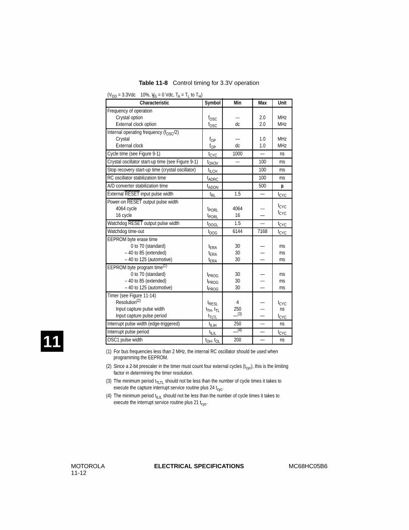
MOTOROLA11-12
MC68HC05B6ELECTRICAL SPECIFICATIONS
11(1) For bus frequencies less than 2 MHz, the internal RC oscillator should be used when
programming the EEPROM.
(2) Since a 2-bit prescaler in the timer must count four external cycles (tcyc), this is the limitingfactor in determining the timer resolution.
(3) The minimum period tTLTL should not be less than the number of cycle times it takes toexecute the capture interrupt service routine plus 24 tcyc.
(4) The minimum period tILIL should not be less than the number of cycle times it takes toexecute the interrupt service routine plus 21 tcyc.
Table 11-8 Control timing for 3.3V operation
(VDD = 3.3Vdc ± 10%, VSS = 0 Vdc, TA = TL to TH)
Characteristic Symbol Min Max Unit
Frequency of operationCrystal optionExternal clock option
fOSCfOSC
—dc
2.02.0
MHzMHz
Internal operating frequency (fOSC/2)CrystalExternal clock
fOPfOP
—dc
1.01.0
MHzMHz
Cycle time (see Figure 9-1) tCYC 1000 — ns
Crystal oscillator start-up time (see Figure 9-1) tOXOV — 100 ms
Stop recovery start-up time (crystal oscillator) tILCH 100 ms
RC oscillator stabilization time tADRC 100 ms
A/D converter stabilization time tADON 500 µs
External RESET input pulse width tRL 1.5 — tCYC
Power-on RESET output pulse width4064 cycle16 cycle
tPORLtPORL
406416
——
tCYCtCYC
Watchdog RESET output pulse width tDOGL 1.5 — tCYC
Watchdog time-out tDOG 6144 7168 tCYC
EEPROM byte erase time0 to 70 (standard)
– 40 to 85 (extended)– 40 to 125 (automotive)
tERAtERAtERA
303030
———
msmsms
EEPROM byte program time(1)
0 to 70 (standard)– 40 to 85 (extended)– 40 to 125 (automotive)
tPROGtPROGtPROG
303030
———
msmsms
Timer (see Figure 11-14)Resolution(2)
Input capture pulse widthInput capture pulse period
tRESLtTH, tTLtTLTL
4250—(3)
———
tCYCns
tCYC
Interrupt pulse width (edge-triggered) tILIH 250 — ns
Interrupt pulse period tILIL —(4) — tCYC
OSC1 pulse width tOH, tOL 200 — ns
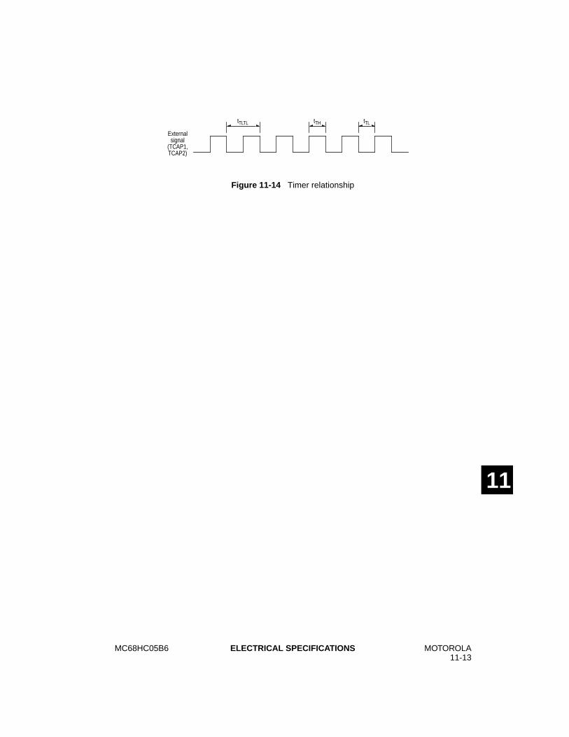
MC68HC05B6 MOTOROLA11-13
ELECTRICAL SPECIFICATIONS
11
Figure 11-14 Timer relationship
Externalsignal
(TCAP1,TCAP2)
tTLTL tTH tTL

MOTOROLA11-14
MC68HC05B6ELECTRICAL SPECIFICATIONS
THIS PAGE INTENTIONALLY LEFT BLANK
11
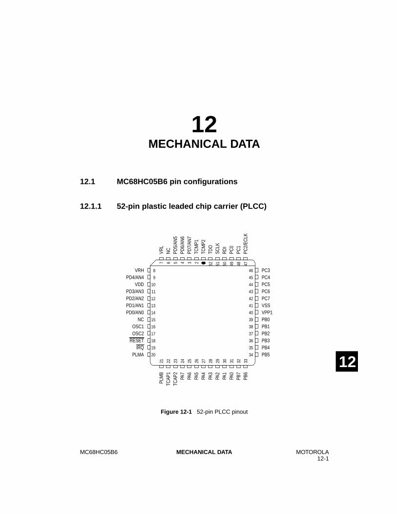
MC68HC05B6 MOTOROLA12-1
MECHANICAL DATA
12
12MECHANICAL DATA
12.1 MC68HC05B6 pin configurations
12.1.1 52-pin plastic leaded chip carrier (PLCC)
Figure 12-1 52-pin PLCC pinout
PC3PC4PC5PC6PC7VSSVPP1PB0PB1PB2PB3PB4PB5
VRHPD4/AN4
VDDPD3/AN3PD2/AN2PD1/AN1PD0/AN0
NCOSC1OSC2
RESETIRQ
PLMA
PLM
BTC
AP1
TCAP
2PA
7PA
6PA
5PA
4PA
3PA
2PA
1PA
0PB
7PB
6
VRL
NC
PD5/
AN5
PD6/
AN6
PD7/
AN7
TCM
P1TC
MP2
TDO
SCLK
RD
IPC
0PC
1PC
2/EC
LK
46
45
44
43
42
41
40
39
38
37
36
35
34
8
9
10
11
12
13
14
15
16
17
18
19
20
21 22 23 24 25 26 27 28 29 30 31 32 33
7 6 5 4 3 2 52 51 50 49 48 47
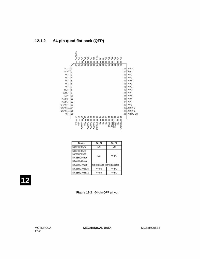
MOTOROLA12-2
MC68HC05B6MECHANICAL DATA
12
12.1.2 64-pin quad flat pack (QFP)
Figure 12-2 64-pin QFP pinout
NC
PB0
NC
VPP1
17 18 20 21 22 23 24 25 26 27 29 30 31 3219
4847
45444342414039383736353433
46
PB6PB7
NCPA0PA1PA2PA3PA4PA5PA6PA7NCTCAP2TCAP1PLMB D/A
NC
PC1PC0
NCNCNCNCRDI
SCLKTDO
TCMP2TCMP1
PD7/AN7PD6/AN6PD5/AN5
NC
NCVR
LVR
H
VDD
PD3/
AN3
PD2/
AN2
PD1/
AN1
NC
NC
NC
OSC
1O
SC2
RES
ET IRQ
PLM
A D
/A
PD4/
AN4
PC2/
ECLK
PC3
PC5
PC6
PC7
VSS
PB1
PB2
PB3
PB4
PB5
PC4
12
45678910111213141516
3
PD0/
AN0
28
64 63 61 60 59 58 56 55 54 53 52 51 50 4962 57
Device Pin 27 Pin 57
MC68HC05B4 NC NC
MC68HC05B6MC68HC05B8MC68HC05B16MC68HC05B32
NC VPP1
MC68HC705B5 Not available in this package
MC68HC705B16 VPP6 VPP1
MC68HC705B32 VPP6 VPP1
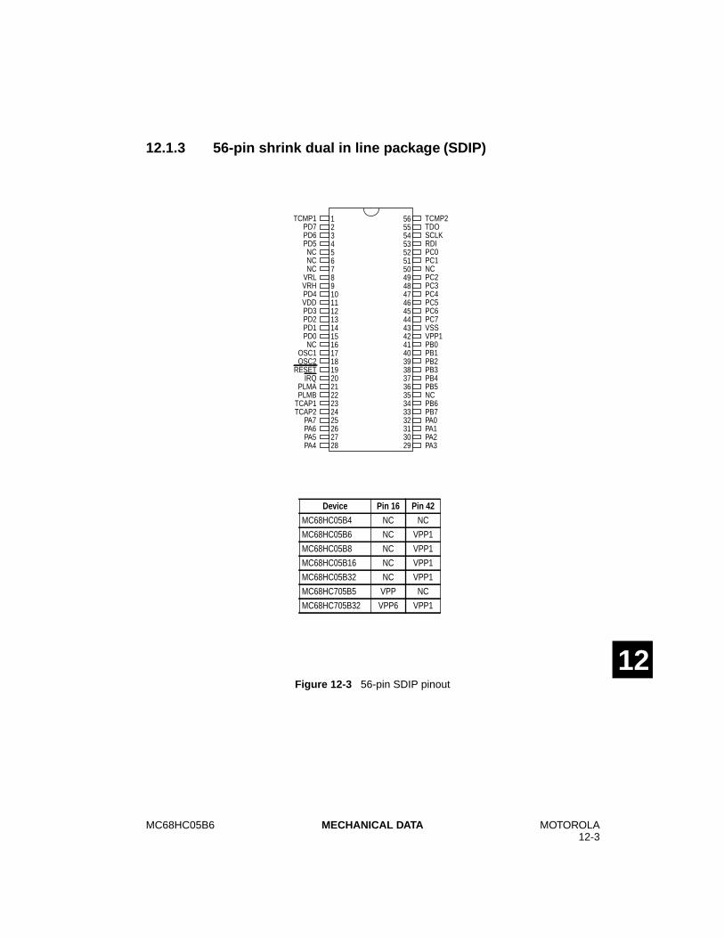
MC68HC05B6 MOTOROLA12-3
MECHANICAL DATA
12
12.1.3 56-pin shrink dual in line package (SDIP)
Figure 12-3 56-pin SDIP pinout
123456789101112131415161718192021
TCMP1PD7PD6PD5NCNCNC
VRLVRHPD4VDDPD3PD2PD1PD0NC
OSC1OSC2
RESETIRQ
PLMA22232425262728
56 TCMP2TDOSCLKRDIPC0PC1NCPC2PC3PC4PC5PC6PC7VSSVPP1PB0PB1PB2PB3PB4PB5
555453525150494847464544434241403938373635343332313029
PLMBTCAP1TCAP2
PA7PA6PA5PA4
NCPB6PB7PA0PA1PA2PA3
Device Pin 16 Pin 42
MC68HC05B4 NC NC
MC68HC05B6 NC VPP1
MC68HC05B8 NC VPP1
MC68HC05B16 NC VPP1
MC68HC05B32 NC VPP1
MC68HC705B5 VPP NC
MC68HC705B32 VPP6 VPP1
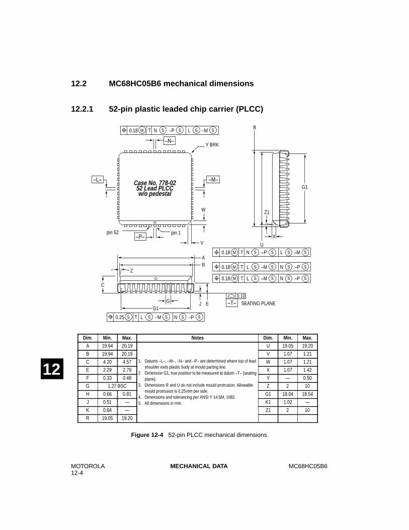
MOTOROLA12-4
MC68HC05B6MECHANICAL DATA
12
12.2 MC68HC05B6 mechanical dimensions
12.2.1 52-pin plastic leaded chip carrier (PLCC)
Figure 12-4 52-pin PLCC mechanical dimensions
–L– –M–
–P–
–N–
pin 1pin 52
V
W
Y BRK
ZRA
C
J EGG1
U
B
G1
Z1
X
0.10–T– SEATING PLANE
0.18 T N –P L –MM SS S S
Case No. 778-0252 Lead PLCCw/o pedestal
Dim. Min. Max. Notes Dim. Min. Max.
A 19.94 20.19
1. Datums –L–, –M–, –N– and –P– are determined where top of leadshoulder exits plastic body at mould parting line.
2. Dimension G1, true position to be measured at datum –T– (seatingplane).
3. Dimensions R and U do not include mould protrusion. Allowablemould protrusion is 0.25mm per side.
4. Dimensions and tolerancing per ANSI Y 14.5M, 1982.5. All dimensions in mm.
U 19.05 19.20
B 19.94 20.19 V 1.07 1.21
C 4.20 4.57 W 1.07 1.21
E 2.29 2.79 X 1.07 1.42
F 0.33 0.48 Y — 0.50
G 1.27 BSC Z 2 10
H 0.66 0.81 G1 18.04 18.54
J 0.51 — K1 1.02 —
K 0.64 — Z1 2 10
R 19.05 19.20
0.18 T L –M N –PM SS S S
0.18 T L –M N –PM SS S S
0.18 T N –P L –MM SS S S
0.25 T L –M N –PS SS S S
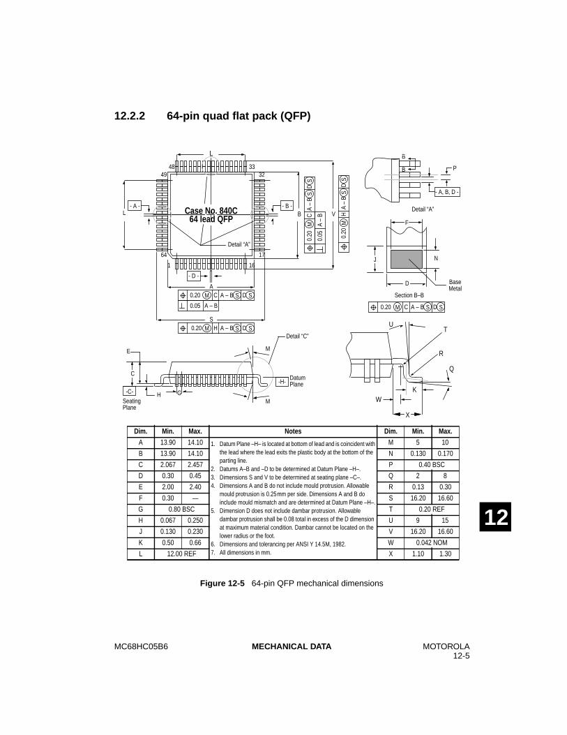
MC68HC05B6 MOTOROLA12-5
MECHANICAL DATA
12
12.2.2 64-pin quad flat pack (QFP)
Figure 12-5 64-pin QFP mechanical dimensions
64 lead QFP
0.20 M C A – B S D S
L
3348
161
32
17
49
64
- B -B V
0.05 A – B
- D -
A
S0.20 M H A – B S D S
L- A -
Detail “A”
B
B
- A, B, D -
P
Detail “A”
F
NJ
D
Section B–B
BaseMetal
GH
E
C
-C-
M
Detail “C”
M
-H-DatumPlane
SeatingPlane
UT
R
Q
KW
X
Dim. Min. Max. Notes Dim. Min. Max.
A 13.90 14.10 1. Datum Plane –H– is located at bottom of lead and is coincident withthe lead where the lead exits the plastic body at the bottom of theparting line.
2. Datums A–B and –D to be determined at Datum Plane –H–.3. Dimensions S and V to be determined at seating plane –C–.4. Dimensions A and B do not include mould protrusion. Allowable
mould protrusion is 0.25mm per side. Dimensions A and B doinclude mould mismatch and are determined at Datum Plane –H–.
5. Dimension D does not include dambar protrusion. Allowabledambar protrusion shall be 0.08 total in excess of the D dimensionat maximum material condition. Dambar cannot be located on thelower radius or the foot.
6. Dimensions and tolerancing per ANSI Y 14.5M, 1982.7. All dimensions in mm.
M 5 10
B 13.90 14.10 N 0.130 0.170
C 2.067 2.457 P 0.40 BSC
D 0.30 0.45 Q 2 8
E 2.00 2.40 R 0.13 0.30
F 0.30 — S 16.20 16.60
G 0.80 BSC T 0.20 REF
H 0.067 0.250 U 9 15
J 0.130 0.230 V 16.20 16.60
K 0.50 0.66 W 0.042 NOM
L 12.00 REF X 1.10 1.30
0.20
MC
A –
BS
DS
0.05
A –
B
0.20
MH
A –
BS
DS
0.20 M C A – B S D S
Case No. 840C
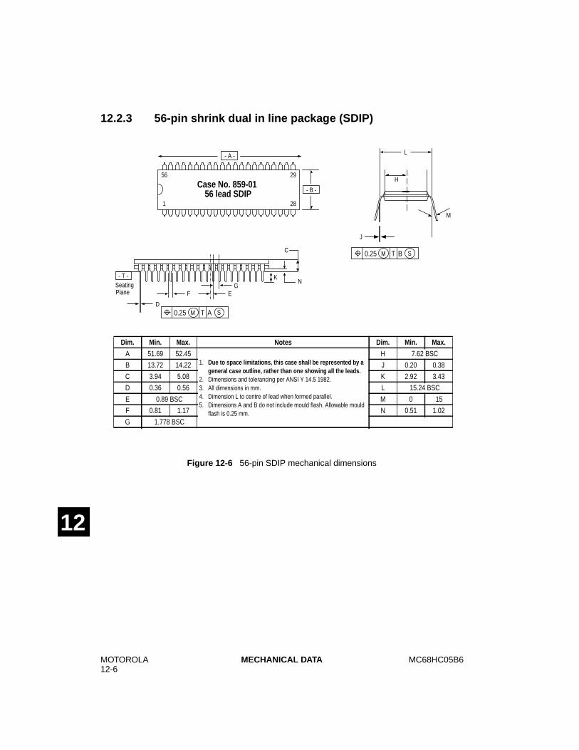
MOTOROLA12-6
MC68HC05B6MECHANICAL DATA
12
12.2.3 56-pin shrink dual in line package (SDIP)
Figure 12-6 56-pin SDIP mechanical dimensions
1 28
56 29
- A -
NG
D
F
L
M
PlaneSeating
C
Dim. Min. Max. Notes Dim. Min. Max.
A 51.69 52.451. Due to space limitations, this case shall be represented by a
general case outline, rather than one showing all the leads.2. Dimensions and tolerancing per ANSI Y 14.5 1982.3. All dimensions in mm.4. Dimension L to centre of lead when formed parallel.5. Dimensions A and B do not include mould flash. Allowable mould
flash is 0.25 mm.
H 7.62 BSC
B 13.72 14.22 J 0.20 0.38
C 3.94 5.08 K 2.92 3.43
D 0.36 0.56 L 15.24 BSC
E 0.89 BSC M 0¡ 15¡
F 0.81 1.17 N 0.51 1.02
G 1.778 BSC
Case No. 859-0156 lead SDIP - B -
H
K- T -
0.25 T AM S
0.25 T BM S
J
E
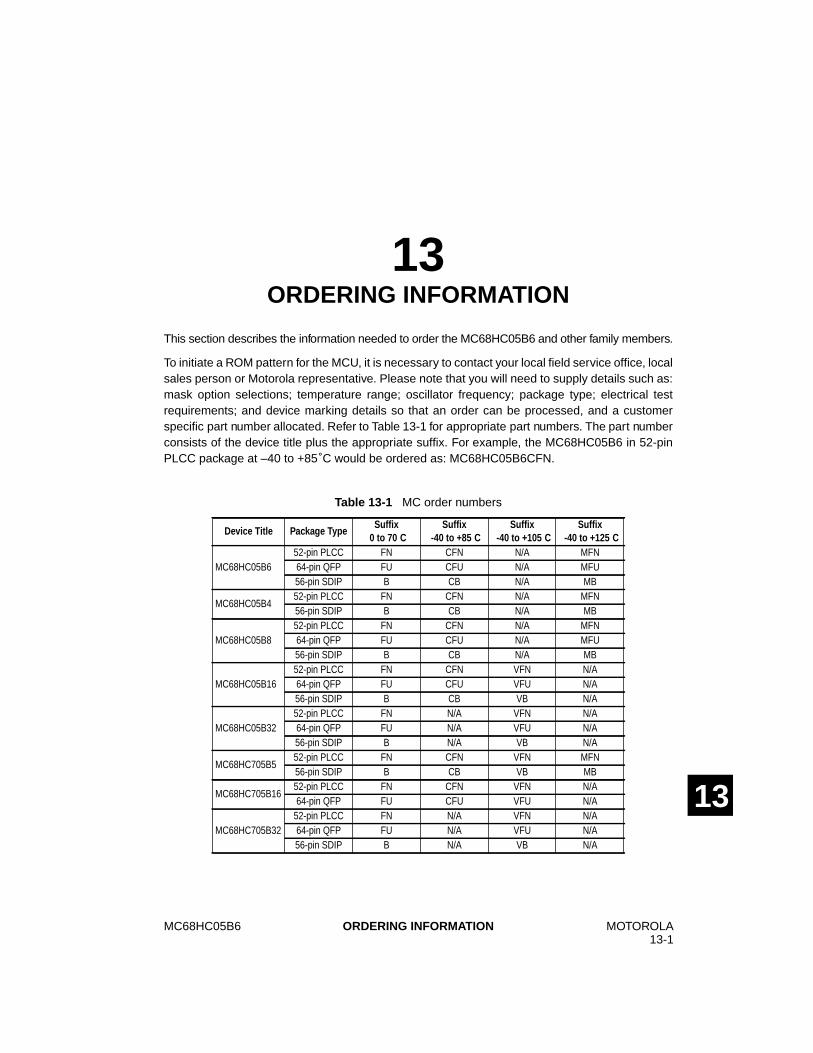
MC68HC05B6 MOTOROLA13-1
ORDERING INFORMATION
13
13ORDERING INFORMATION
This section describes the information needed to order the MC68HC05B6 and other family members.
To initiate a ROM pattern for the MCU, it is necessary to contact your local field service office, localsales person or Motorola representative. Please note that you will need to supply details such as:mask option selections; temperature range; oscillator frequency; package type; electrical testrequirements; and device marking details so that an order can be processed, and a customerspecific part number allocated. Refer to Table 13-1 for appropriate part numbers. The part numberconsists of the device title plus the appropriate suffix. For example, the MC68HC05B6 in 52-pinPLCC package at –40 to +85˚C would be ordered as: MC68HC05B6CFN.
Table 13-1 MC order numbers
Device Title Package TypeSuffix
0 to 70¡CSuffix
-40 to +85¡CSuffix
-40 to +105¡CSuffix
-40 to +125¡C
MC68HC05B652-pin PLCC FN CFN N/A MFN64-pin QFP FU CFU N/A MFU56-pin SDIP B CB N/A MB
MC68HC05B452-pin PLCC FN CFN N/A MFN56-pin SDIP B CB N/A MB
MC68HC05B852-pin PLCC FN CFN N/A MFN64-pin QFP FU CFU N/A MFU56-pin SDIP B CB N/A MB
MC68HC05B1652-pin PLCC FN CFN VFN N/A64-pin QFP FU CFU VFU N/A56-pin SDIP B CB VB N/A
MC68HC05B3252-pin PLCC FN N/A VFN N/A64-pin QFP FU N/A VFU N/A56-pin SDIP B N/A VB N/A
MC68HC705B552-pin PLCC FN CFN VFN MFN56-pin SDIP B CB VB MB
MC68HC705B1652-pin PLCC FN CFN VFN N/A64-pin QFP FU CFU VFU N/A
MC68HC705B3252-pin PLCC FN N/A VFN N/A64-pin QFP FU N/A VFU N/A56-pin SDIP B N/A VB N/A
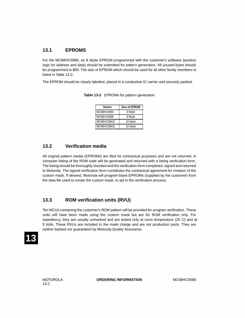
MOTOROLA13-2
MC68HC05B6ORDERING INFORMATION
13
13.1 EPROMS
For the MC68HC05B6, an 8 kbyte EPROM programmed with the customer’s software (positivelogic for address and data) should be submitted for pattern generation. All unused bytes shouldbe programmed to $00. The size of EPROM which should be used for all other family members islisted in Table 13-2.
The EPROM should be clearly labelled, placed in a conductive IC carrier and securely packed.
13.2 Verification media
All original pattern media (EPROMs) are filed for contractual purposes and are not returned. Acomputer listing of the ROM code will be generated and returned with a listing verification form.The listing should be thoroughly checked and the verification form completed, signed and returnedto Motorola. The signed verification form constitutes the contractual agreement for creation of thecustom mask. If desired, Motorola will program blank EPROMs (supplied by the customer) fromthe data file used to create the custom mask, to aid in the verification process.
13.3 ROM verification units (RVU)
Ten MCUs containing the customer’s ROM pattern will be provided for program verification. Theseunits will have been made using the custom mask but are for ROM verification only. Forexpediency, they are usually unmarked and are tested only at room temperature (25¡C) and at5 Volts. These RVUs are included in the mask charge and are not production parts. They areneither backed nor guaranteed by Motorola Quality Assurance.
Table 13-2 EPROMs for pattern generation
Device Size of EPROM
MC68HC05B4 8 kbyte
MC68HC05B8 8 kbyte
MC68HC05B16 16 kbyte
MC68HC05B32 32 kbyte
MC68HC05B6 MOTOROLAA-1
MC68HC05B4
14
AMC68HC05B4
The MC68HC05B4 is a device similar to the MC68HC05B6, but without EEPROM and having areduced ROM size of 4 kbytes. The entire MC68HC05B6 data sheet applies to the MC68HC05B4,with the exceptions outlined in this appendix.
Features
• 4158 bytes User ROM (including 14 bytes User vectors)
• No EEPROM
Section 3.5, ‘EEPROM’, therefore, does not apply to the MC68HC05B4, and the register ataddress $07 only allows the user to select whether or not the ECLK should appear at PC2, usingbit 3 of $07. All other bits of this register read as ‘0’.
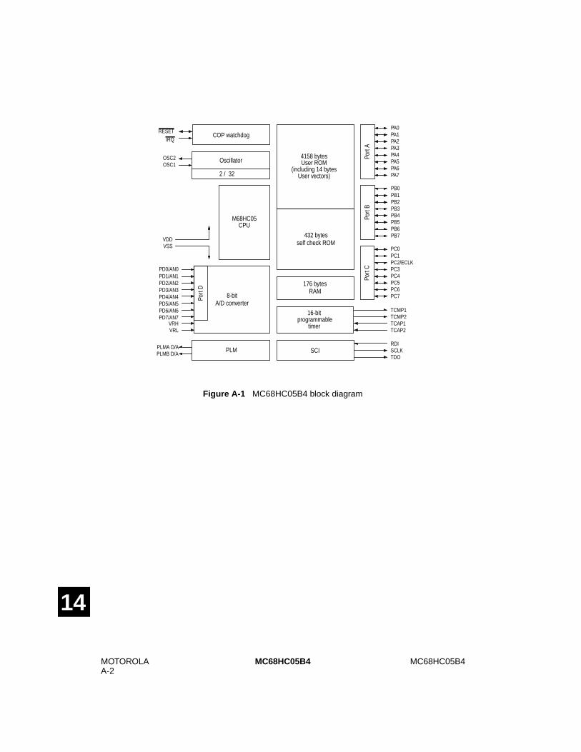
MOTOROLAA-2
MC68HC05B4MC68HC05B4
14
Figure A-1 MC68HC05B4 block diagram
Port
A
PA0PA1PA2PA3PA4PA5PA6PA7
Port
B
PB0PB1PB2PB3PB4PB5PB6PB7
Port
C
PC0PC1PC2/ECLKPC3PC4PC5PC6PC7
16-bitprogrammable
timer
Port
D
PD0/AN0PD1/AN1PD2/AN2PD3/AN3PD4/AN4PD5/AN5PD6/AN6PD7/AN7
Oscillator
176 bytesRAM
COP watchdogRESET
IRQ
VDDVSS
OSC1OSC2
M68HC05CPU
SCI
A/D converter
PLM
TCAP1TCAP2
TCMP1TCMP2
VRHVRL
RDISCLKTDO
2 / 32
PLMA D/APLMB D/A
8-bit
432 bytes
User ROM4158 bytes
self check ROM
(including 14 bytesUser vectors)
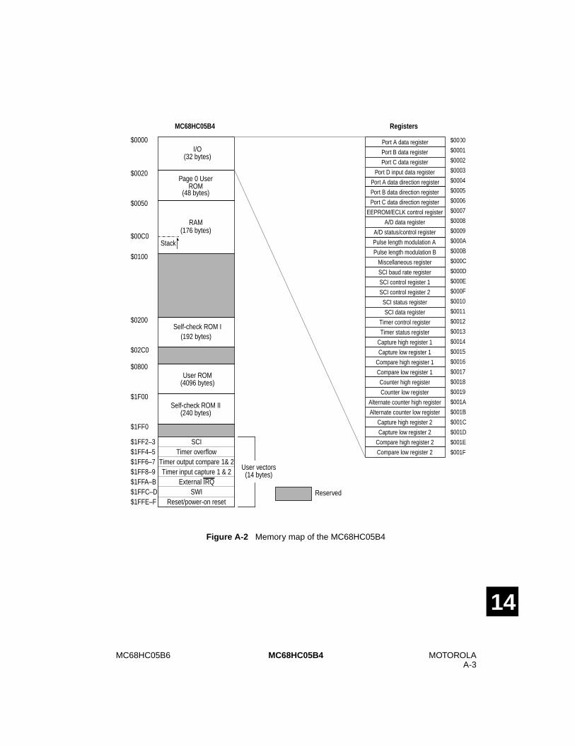
MC68HC05B6 MOTOROLAA-3
MC68HC05B4
14
Figure A-2 Memory map of the MC68HC05B4
User vectors(14 bytes)
$1FF2–3 SCITimer overflow
Timer output compare 1& 2Timer input capture 1 & 2
External IRQSWI
Reset/power-on reset
Port B data register
Port C data register
Port D input data register
Port A data register $0000
Compare low register 2
A/D data register
$0000I/O
(32 bytes)
$0020
$00C0
$0100
$1FF0
Stack
RAM(176 bytes)
$02C0
$0200
$1F00
$0050
Port A data direction register
Port B data direction register
Port C data direction register
EEPROM/ECLK control register
A/D status/control register
Pulse length modulation A
Pulse length modulation B
Miscellaneous register
SCI baud rate register
SCI control register 1
SCI control register 2
SCI status register
SCI data register
Timer control register
Timer status register
Capture high register 1
Capture low register 1
Compare high register 1
Compare low register 1
Counter high register
Counter low register
Alternate counter high register
Alternate counter low register
Capture high register 2
Capture low register 2
Compare high register 2
$0001
$0002
$0003
$0004
$0005
$0006
$0007
$0008
$0009
$000A
$000B
$000C
$000D
$000E
$000F
$0010
$0011
$0012
$0013
$0014
$0015
$0016
$0017
$0018
$0019
$001A
$001B
$001C
$001D
$001E
$001F
Page 0 UserROM
(48 bytes)
Self-check ROM I(192 bytes)
User ROM(4096 bytes)
Self-check ROM II(240 bytes)
$0800
Reserved
MC68HC05B4 Registers
$1FF4–5$1FF6–7$1FF8–9$1FFA–B$1FFC–D$1FFE–F
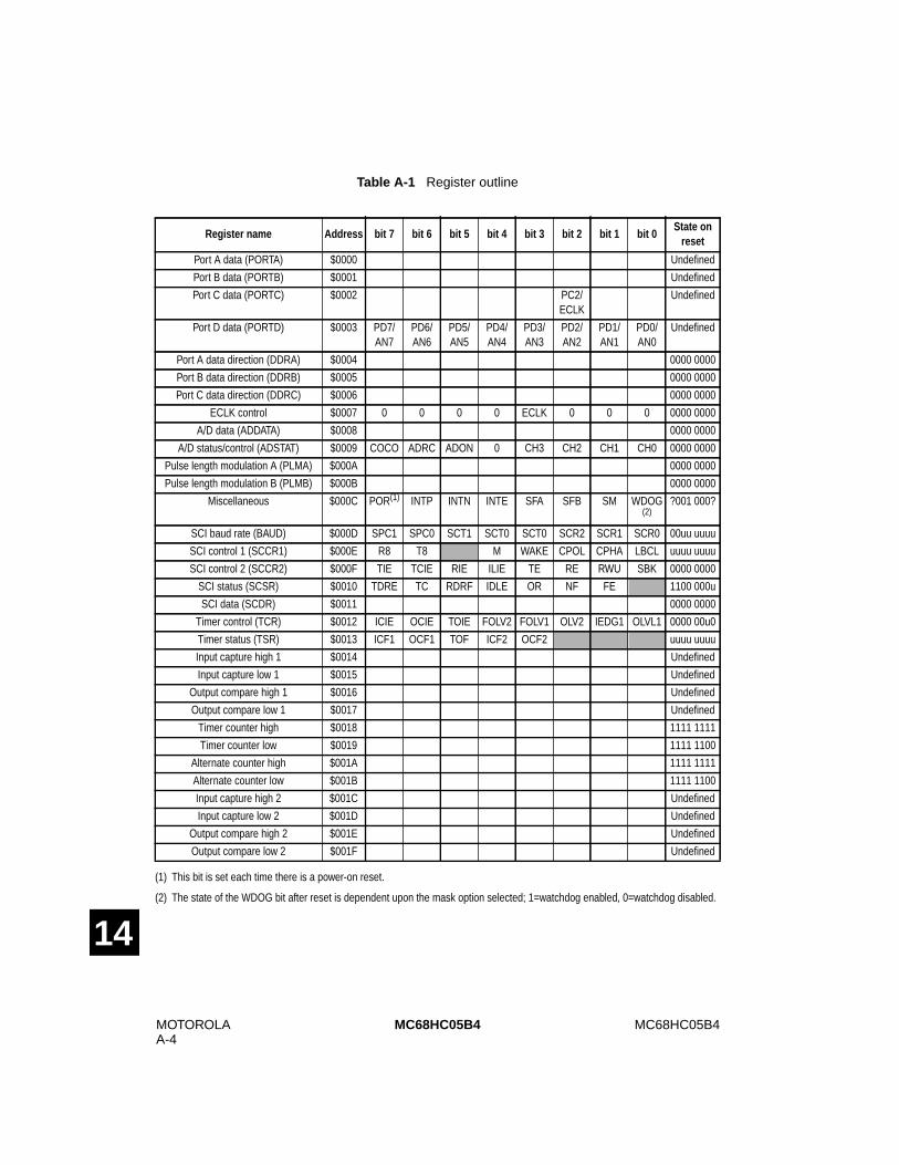
MOTOROLAA-4
MC68HC05B4MC68HC05B4
14
(1) This bit is set each time there is a power-on reset.
(2) The state of the WDOG bit after reset is dependent upon the mask option selected; 1=watchdog enabled, 0=watchdog disabled.
Table A-1 Register outline
Register name Address bit 7 bit 6 bit 5 bit 4 bit 3 bit 2 bit 1 bit 0State on
reset
Port A data (PORTA) $0000 Undefined
Port B data (PORTB) $0001 Undefined
Port C data (PORTC) $0002 PC2/ECLK
Undefined
Port D data (PORTD) $0003 PD7/AN7
PD6/AN6
PD5/AN5
PD4/AN4
PD3/AN3
PD2/AN2
PD1/AN1
PD0/AN0
Undefined
Port A data direction (DDRA) $0004 0000 0000
Port B data direction (DDRB) $0005 0000 0000
Port C data direction (DDRC) $0006 0000 0000
ECLK control $0007 0 0 0 0 ECLK 0 0 0 0000 0000
A/D data (ADDATA) $0008 0000 0000
A/D status/control (ADSTAT) $0009 COCO ADRC ADON 0 CH3 CH2 CH1 CH0 0000 0000
Pulse length modulation A (PLMA) $000A 0000 0000
Pulse length modulation B (PLMB) $000B 0000 0000
Miscellaneous $000C POR(1) INTP INTN INTE SFA SFB SM WDOG(2)
?001 000?
SCI baud rate (BAUD) $000D SPC1 SPC0 SCT1 SCT0 SCT0 SCR2 SCR1 SCR0 00uu uuuu
SCI control 1 (SCCR1) $000E R8 T8 M WAKE CPOL CPHA LBCL uuuu uuuu
SCI control 2 (SCCR2) $000F TIE TCIE RIE ILIE TE RE RWU SBK 0000 0000
SCI status (SCSR) $0010 TDRE TC RDRF IDLE OR NF FE 1100 000u
SCI data (SCDR) $0011 0000 0000
Timer control (TCR) $0012 ICIE OCIE TOIE FOLV2 FOLV1 OLV2 IEDG1 OLVL1 0000 00u0
Timer status (TSR) $0013 ICF1 OCF1 TOF ICF2 OCF2 uuuu uuuu
Input capture high 1 $0014 Undefined
Input capture low 1 $0015 Undefined
Output compare high 1 $0016 Undefined
Output compare low 1 $0017 Undefined
Timer counter high $0018 1111 1111
Timer counter low $0019 1111 1100
Alternate counter high $001A 1111 1111
Alternate counter low $001B 1111 1100
Input capture high 2 $001C Undefined
Input capture low 2 $001D Undefined
Output compare high 2 $001E Undefined
Output compare low 2 $001F Undefined
MC68HC05B6 MOTOROLAB-1
MC68HC05B8
14
BMC68HC05B8
The MC68HC05B8 is a device similar to the MC68HC05B6, but with an increased ROM size of7.25 kbytes. The entire MC68HC05B6 data sheet applies to the MC68HC05B8, with theexceptions outlined in this appendix.
Features
• 7230 bytes User ROM (including 14 bytes User vectors)
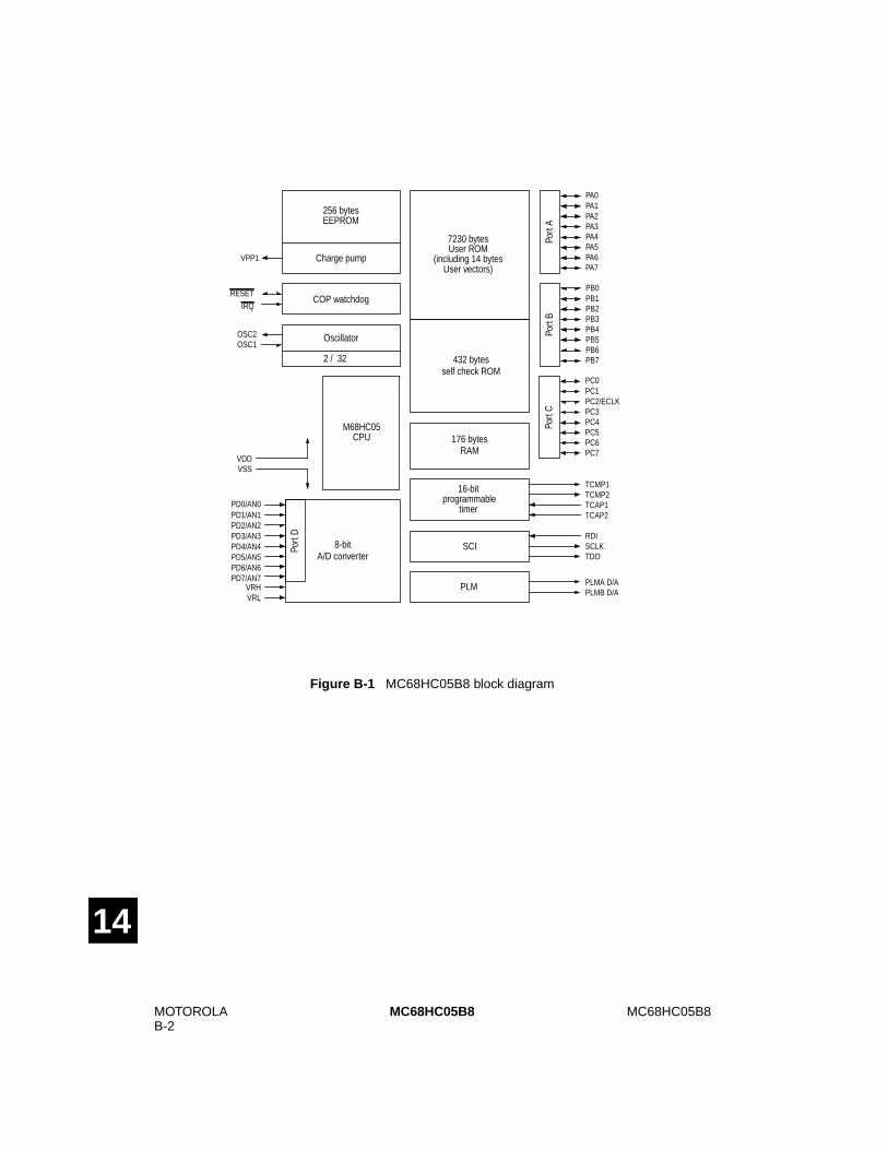
MOTOROLAB-2
MC68HC05B8MC68HC05B8
14
Figure B-1 MC68HC05B8 block diagram
Port
A
PA0PA1PA2PA3PA4PA5PA6PA7
Port
B
PB0PB1PB2PB3PB4PB5PB6PB7
Port
C
PC0PC1PC2/ECLKPC3PC4PC5PC6PC7
16-bitprogrammable
timer
Port
D
PD0/AN0PD1/AN1PD2/AN2PD3/AN3PD4/AN4PD5/AN5PD6/AN6PD7/AN7
Oscillator
176 bytesRAM
COP watchdogRESET
IRQ
VDDVSS
OSC1OSC2
M68HC05CPU
SCIA/D converter
PLM
TCAP1TCAP2
TCMP1TCMP2
VRHVRL
RDISCLKTDO
VPP1
256 bytesEEPROM
Charge pump
2 / 32
PLMA D/APLMB D/A
8-bit
432 bytes
User ROM7230 bytes
self check ROM
(including 14 bytesUser vectors)
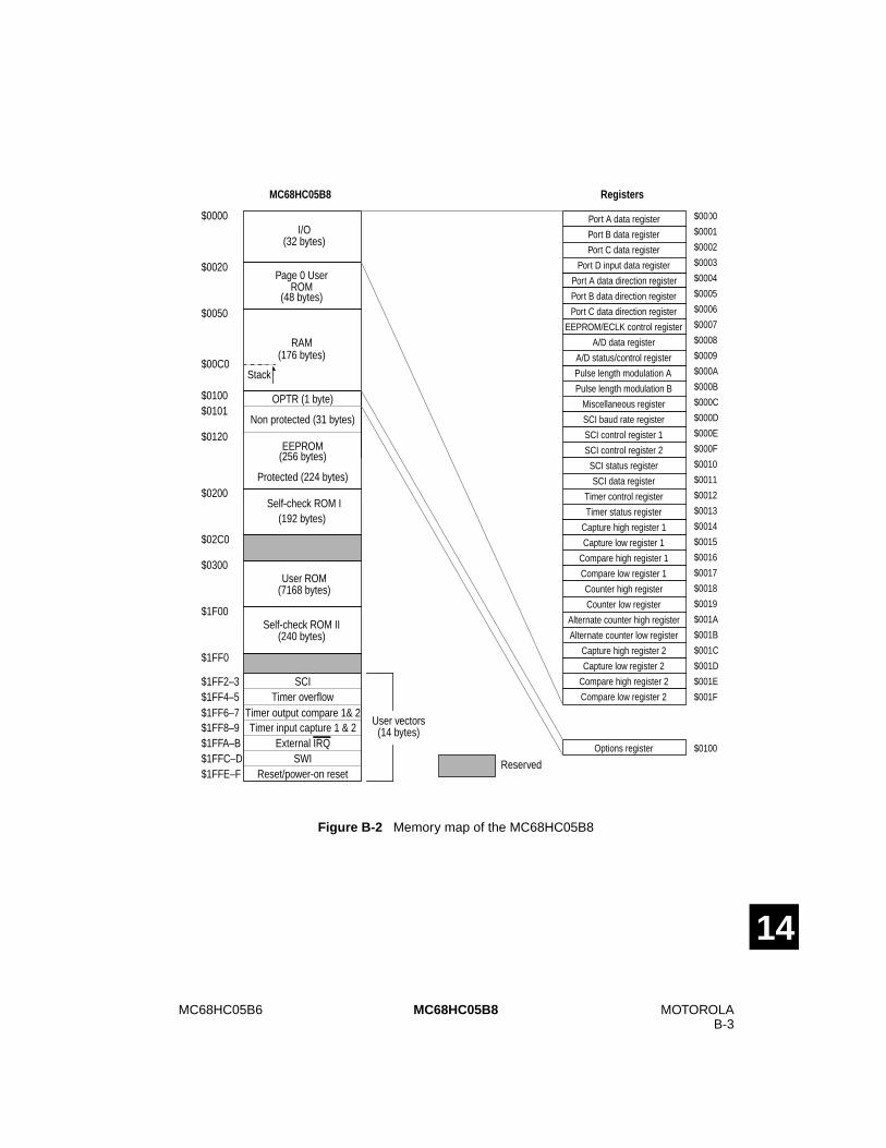
MC68HC05B6 MOTOROLAB-3
MC68HC05B8
14
Figure B-2 Memory map of the MC68HC05B8
Port B data register
Port C data register
Port D input data register
Port A data register $0000
Compare low register 2
A/D data register
$0000I/O
(32 bytes)
$0020
$00C0
$0100
$1FF0
Stack
RAM(176 bytes)
$02C0
$0200
$1F00
$0050
Port A data direction register
Port B data direction register
Port C data direction register
EEPROM/ECLK control register
A/D status/control register
Pulse length modulation A
Pulse length modulation B
Miscellaneous register
SCI baud rate register
SCI control register 1
SCI control register 2
SCI status register
SCI data register
Timer control register
Timer status register
Capture high register 1
Capture low register 1
Compare high register 1
Compare low register 1
Counter high register
Counter low register
Alternate counter high register
Alternate counter low register
Capture high register 2
Capture low register 2
Compare high register 2
$0001
$0002
$0003
$0004
$0005
$0006
$0007
$0008
$0009
$000A
$000B
$000C
$000D
$000E
$000F
$0010
$0011
$0012
$0013
$0014
$0015
$0016
$0017
$0018
$0019
$001A
$001B
$001C
$001D
$001E
$001F
Page 0 UserROM
(48 bytes)
Self-check ROM I(192 bytes)
User ROM(7168 bytes)
Self-check ROM II(240 bytes)
$0300
OPTR (1 byte)
Non protected (31 bytes)
Protected (224 bytes)
EEPROM(256 bytes)
$0101
$0120
$0100Options register
Reserved
MC68HC05B8 Registers
User vectors(14 bytes)
$1FF2–3 SCITimer overflow
Timer output compare 1& 2Timer input capture 1 & 2
External IRQSWI
Reset/power-on reset
$1FF4–5$1FF6–7$1FF8–9$1FFA–B$1FFC–D$1FFE–F
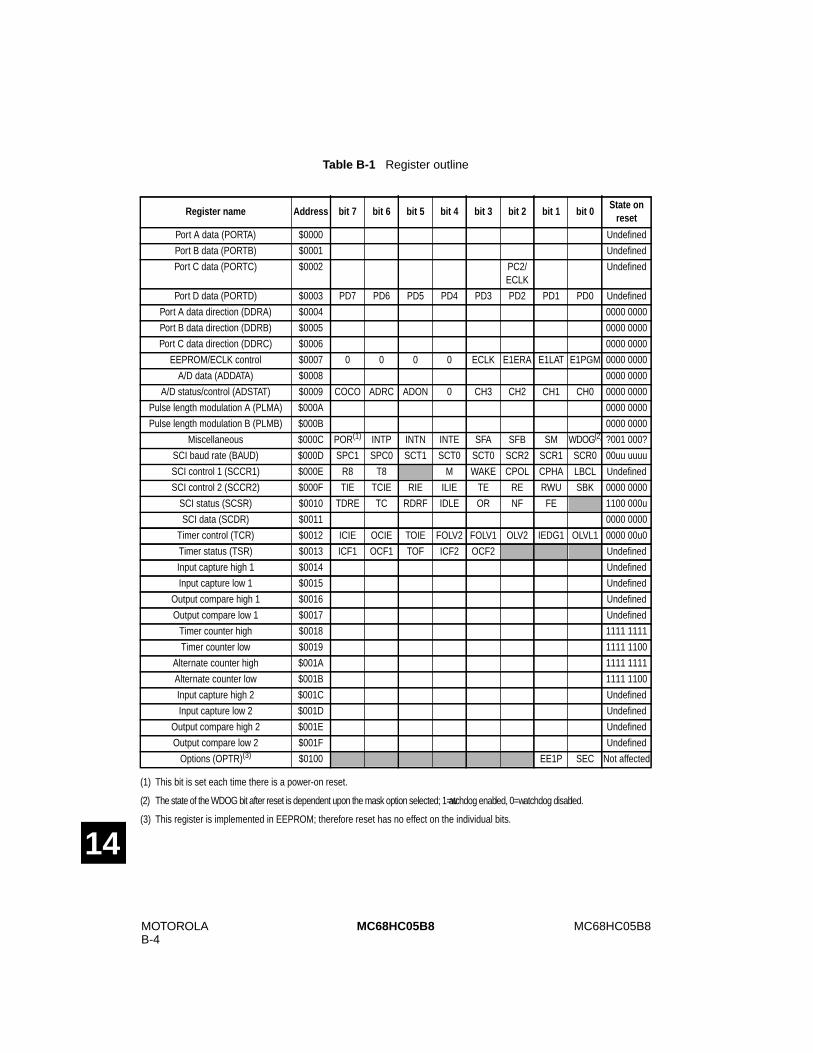
MOTOROLAB-4
MC68HC05B8MC68HC05B8
14
(1) This bit is set each time there is a power-on reset.
(2) The state of the WDOG bit after reset is dependent upon the mask option selected; 1=watchdog enabled, 0=watchdog disabled.
(3) This register is implemented in EEPROM; therefore reset has no effect on the individual bits.
Table B-1 Register outline
Register name Address bit 7 bit 6 bit 5 bit 4 bit 3 bit 2 bit 1 bit 0State on
reset
Port A data (PORTA) $0000 Undefined
Port B data (PORTB) $0001 Undefined
Port C data (PORTC) $0002 PC2/ECLK
Undefined
Port D data (PORTD) $0003 PD7 PD6 PD5 PD4 PD3 PD2 PD1 PD0 Undefined
Port A data direction (DDRA) $0004 0000 0000
Port B data direction (DDRB) $0005 0000 0000
Port C data direction (DDRC) $0006 0000 0000
EEPROM/ECLK control $0007 0 0 0 0 ECLK E1ERA E1LAT E1PGM 0000 0000
A/D data (ADDATA) $0008 0000 0000
A/D status/control (ADSTAT) $0009 COCO ADRC ADON 0 CH3 CH2 CH1 CH0 0000 0000
Pulse length modulation A (PLMA) $000A 0000 0000
Pulse length modulation B (PLMB) $000B 0000 0000
Miscellaneous $000C POR(1) INTP INTN INTE SFA SFB SM WDOG(2) ?001 000?
SCI baud rate (BAUD) $000D SPC1 SPC0 SCT1 SCT0 SCT0 SCR2 SCR1 SCR0 00uu uuuu
SCI control 1 (SCCR1) $000E R8 T8 M WAKE CPOL CPHA LBCL Undefined
SCI control 2 (SCCR2) $000F TIE TCIE RIE ILIE TE RE RWU SBK 0000 0000
SCI status (SCSR) $0010 TDRE TC RDRF IDLE OR NF FE 1100 000u
SCI data (SCDR) $0011 0000 0000
Timer control (TCR) $0012 ICIE OCIE TOIE FOLV2 FOLV1 OLV2 IEDG1 OLVL1 0000 00u0
Timer status (TSR) $0013 ICF1 OCF1 TOF ICF2 OCF2 Undefined
Input capture high 1 $0014 Undefined
Input capture low 1 $0015 Undefined
Output compare high 1 $0016 Undefined
Output compare low 1 $0017 Undefined
Timer counter high $0018 1111 1111
Timer counter low $0019 1111 1100
Alternate counter high $001A 1111 1111
Alternate counter low $001B 1111 1100
Input capture high 2 $001C Undefined
Input capture low 2 $001D Undefined
Output compare high 2 $001E Undefined
Output compare low 2 $001F Undefined
Options (OPTR)(3) $0100 EE1P SEC Not affected
MC68HC05B6 MOTOROLAC-1
MC68HC705B5
14
CMC68HC705B5
The MC68HC705B5 is a device similar to the MC68HC05B6, but with the 6 kbytes ROM and 256bytes EEPROM replaced by a single EPROM array. In addition, the self-check routines availableon the MC68HC05B6 are replaced by bootstrap firmware. The MC68HC705B5 is intended tooperate as a one time programmable (OTP) version of the MC68HC05B6 or the MC68HC05B4,meaning that the application program can never be erased once it has been loaded into theEPROM. The entire MC68HC05B6 data sheet applies to the MC68HC705B5, with the exceptionsoutlined in this appendix.
Features
• 6206 bytes EPROM (including 14 bytes User vectors)
• No EEPROM
• Bootstrap firmware
• Simultaneous programming of up to 4 bytes
• Data protection for program code
• Optional pull-down resistors on port B and port C
• Additional temperature range available; -40 to +105¡C
• MC68HC05B6 mask options are programmable using control bits held in the optionsregister
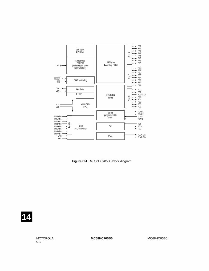
MOTOROLAC-2
MC68HC05B6MC68HC705B5
14
Figure C-1 MC68HC705B5 block diagram
Port
A
PA0PA1PA2PA3PA4PA5PA6PA7
Port
B
PB0PB1PB2PB3PB4PB5PB6PB7
Port
C
PC0PC1PC2/ECLKPC3PC4PC5PC6PC7
16-bitprogrammable
timer
Port
D
PD0/AN0PD1/AN1PD2/AN2PD3/AN3PD4/AN4PD5/AN5PD6/AN6PD7/AN7
Oscillator
176 bytesRAM
COP watchdogRESET
IRQ
VDDVSS
OSC1OSC2
M68HC05CPU
SCIA/D converter
PLM
TCAP1TCAP2
TCMP1TCMP2
VRHVRL
RDISCLKTDO
VPP6
256 bytesEPROM1
6206 bytes
2 / 32
PLMA D/APLMB D/A
8-bit
496 bytesbootstrap ROM
EPROM(including 14 bytes
User vectors)
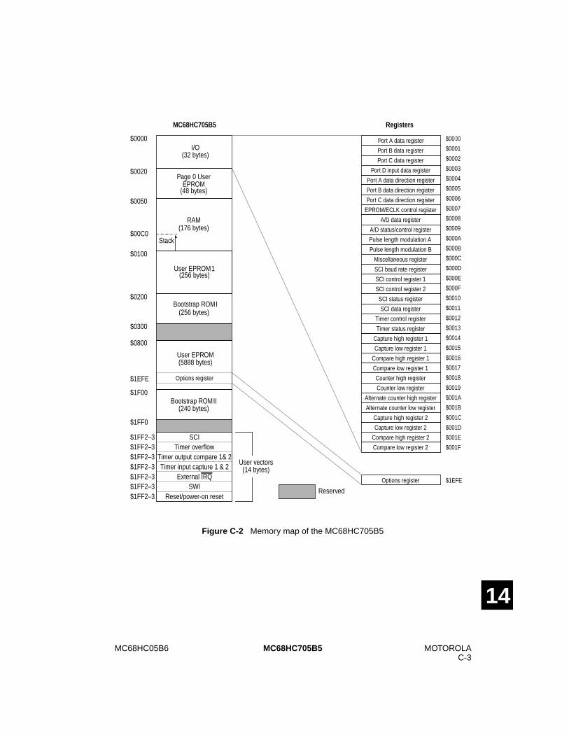
MC68HC05B6 MOTOROLAC-3
MC68HC705B5
14
Figure C-2 Memory map of the MC68HC705B5
Port B data register
Port C data register
Port D input data register
Port A data register $0000
Compare low register 2
A/D data register
$0000I/O
(32 bytes)
$0020
$00C0
$0100
$1FF0
Stack
RAM(176 bytes)
$0300
$0200
$1F00
$0050
Port A data direction register
Port B data direction register
Port C data direction register
EPROM/ECLK control register
A/D status/control register
Pulse length modulation A
Pulse length modulation B
Miscellaneous register
SCI baud rate register
SCI control register 1
SCI control register 2
SCI status register
SCI data register
Timer control register
Timer status register
Capture high register 1
Capture low register 1
Compare high register 1
Compare low register 1
Counter high register
Counter low register
Alternate counter high register
Alternate counter low register
Capture high register 2
Capture low register 2
Compare high register 2
$0001
$0002
$0003
$0004
$0005
$0006
$0007
$0008
$0009
$000A
$000B
$000C
$000D
$000E
$000F
$0010
$0011
$0012
$0013
$0014
$0015
$0016
$0017
$0018
$0019
$001A
$001B
$001C
$001D
$001E
$001F
Page 0 UserEPROM
(48 bytes)
Bootstrap ROMI(256 bytes)
User EPROM(5888 bytes)
Bootstrap ROMII(240 bytes)
$0800
User EPROM1(256 bytes)
$1EFEOptions register
Reserved
MC68HC705B5 Registers
Options register$1EFE
User vectors(14 bytes)
$1FF2–3 SCITimer overflow
Timer output compare 1& 2Timer input capture 1 & 2
External IRQSWI
Reset/power-on reset
$1FF2–3$1FF2–3$1FF2–3$1FF2–3$1FF2–3$1FF2–3
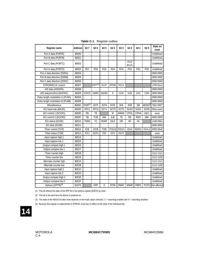
MOTOROLAC-4
MC68HC05B6MC68HC705B5
14
(1) This bit reflects the state of the EPP bit in the options register ($1EFE) at reset.
(2) This bit is set each time the device is powered-on.
(3) The state of the WDOG bit after reset depends on the mask option selected; ‘1’ = watchdog enabled and ‘0’ = watchdog disabled.
(4) Because this register is implemented in EPROM, reset has no effect on the state of the individual bits.
Table C-1 Register outline
Register name Address bit 7 bit 6 bit 5 bit 4 bit 3 bit 2 bit 1 bit 0State on
reset
Port A data (PORTA) $0000 Undefined
Port B data (PORTB) $0001 Undefined
Port C data (PORTC) $0002PC2/ECLK
Undefined
Port D data (PORTD) $0003 PD7 PD6 PD5 PD4 PD3 PD2 PD1 PD0 Undefined
Port A data direction (DDRA) $0004 0000 0000
Port B data direction (DDRB) $0005 0000 0000
Port C data direction (DDRC) $0006 0000 0000
EPROM/ECLK control $0007 EPPT(1) ELAT EPGM ECLK u?00 0uuu
A/D data (ADDATA) $0008 0000 0000
A/D status/control (ADSTAT) $0009 COCO ADRC ADON 0 CH3 CH2 CH1 CH0 0000 0000
Pulse length modulation A (PLMA) $000A 0000 0000
Pulse length modulation B (PLMB) $000B 0000 0000
Miscellaneous $000C POR(2) INTP INTN INTE SFA SFB SM WDOG(3) ?001 000?
SCI baud rate (BAUD) $000D SPC1 SPC0 SCT1 SCT0 SCT0 SCR2 SCR1 SCR0 00uu uuuu
SCI control 1 (SCCR1) $000E R8 T8 M WAKE CPOL CPHA LBCL uuuu
SCI control 2 (SCCR2) $000F TIE TCIE RIE ILIE TE RE RWU SBK 0000 0000
SCI status (SCSR) $0010 TDRE TC RDRF IDLE OR NF FE 1100 000u
SCI data (SCDR) $0011 0000 0000
Timer control (TCR) $0012 ICIE OCIE TOIE FOLV2 FOLV1 OLV2 IEDG1 OLVL1 0000 00u0
Timer status (TSR) $0013 ICF1 OCF1 TOF ICF2 OCF2 uuuu
Input capture high 1 $0014 Undefined
Input capture low 1 $0015 Undefined
Output compare high 1 $0016 Undefined
Output compare low 1 $0017 Undefined
Timer counter high $0018 1111 1111
Timer counter low $0019 1111 1100
Alternate counter high $001A 1111 1111
Alternate counter low $001B 1111 1100
Input capture high 2 $001C Undefined
Input capture low 2 $001D Undefined
Output compare high 2 $001E Undefined
Output compare low 2 $001F Undefined
Options (OPTR)(4) $1EFE EPP 0 RTIM RWAT WWAT PBPD PCPD Not affected
MC68HC05B6 MOTOROLAC-5
MC68HC705B5
14
C.1 EPROM
The MC68HC705B5 has a total of 6206 bytes of EPROM, 256 bytes being reserved for theEPROM1 array (see Figure C-2). The EPP bit (EPROM protect) is not operative on the EPROM1array, making it possible to program it after the main EPROM has been programmed andprotected. The reset and interrupt vectors are located at $1FF2-$1FFF and the EPROM controlregister described in Section C.2.1 is located at address $0007.
The EPROM array is supplied by the VPP6 pin in both read and programming modes. Typicallythe user’s software will be loaded in a programming board where VPP6 is controlled by one of thebootstrap loader routines (bootloader mode). It will then be placed in an application where noprogramming occurs (user mode). In this case the VPP6 pin should be hardwired to VDD.
An erased EPROM byte reads as $00.
Warning: A minimum VDD voltage must be applied to the VPP6 pin at all times, includingpower-on, as a lower voltage could damage the device.
C.1.1 EPROM programming operation
The User program can be used to program some EPROM locations, provided the properprocedure is followed. In particular, the programming sequence must be running in RAM, as theEPROM will not be available for code execution while the ELAT bit is set. The VPP6 switching mustoccur externally, after the EPGM bit is set, for example, under the control of a signal generated ona pin by the programming routine.
Note: When the part becomes a PROM, only the cumulative programming of bits to logic 1 ispossible if multiple programming is made on the same byte.
To allow simultaneous programming of up to 4 bytes, they must be in the same group of addresseswhich share the same most significant address bits; only the two LSBs can change.
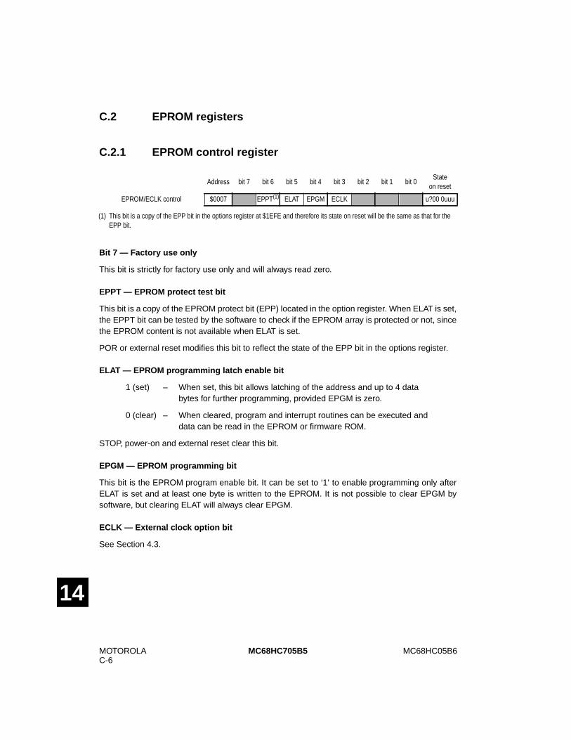
MOTOROLAC-6
MC68HC05B6MC68HC705B5
14
C.2 EPROM registers
C.2.1 EPROM control register
Bit 7 — Factory use only
This bit is strictly for factory use only and will always read zero.
EPPT — EPROM protect test bit
This bit is a copy of the EPROM protect bit (EPP) located in the option register. When ELAT is set,the EPPT bit can be tested by the software to check if the EPROM array is protected or not, sincethe EPROM content is not available when ELAT is set.
POR or external reset modifies this bit to reflect the state of the EPP bit in the options register.
ELAT — EPROM programming latch enable bit
1 (set) – When set, this bit allows latching of the address and up to 4 databytes for further programming, provided EPGM is zero.
0 (clear) – When cleared, program and interrupt routines can be executed anddata can be read in the EPROM or firmware ROM.
STOP, power-on and external reset clear this bit.
EPGM — EPROM programming bit
This bit is the EPROM program enable bit. It can be set to ‘1’ to enable programming only afterELAT is set and at least one byte is written to the EPROM. It is not possible to clear EPGM bysoftware, but clearing ELAT will always clear EPGM.
ECLK — External clock option bit
See Section 4.3.
(1) This bit is a copy of the EPP bit in the options register at $1EFE and therefore its state on reset will be the same as that for theEPP bit.
Address bit 7 bit 6 bit 5 bit 4 bit 3 bit 2 bit 1 bit 0State
on reset
EPROM/ECLK control $0007 EPPT(1) ELAT EPGM ECLK u?00 0uuu
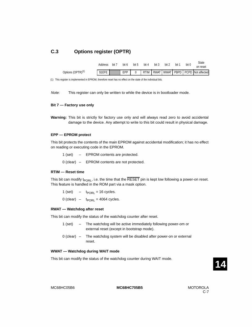
MC68HC05B6 MOTOROLAC-7
MC68HC705B5
14
C.3 Options register (OPTR)
Note: This register can only be written to while the device is in bootloader mode.
Bit 7 — Factory use only
Warning: This bit is strictly for factory use only and will always read zero to avoid accidentaldamage to the device. Any attempt to write to this bit could result in physical damage.
EPP — EPROM protect
This bit protects the contents of the main EPROM against accidental modification; it has no effecton reading or executing code in the EPROM.
1 (set) – EPROM contents are protected.
0 (clear) – EPROM contents are not protected.
RTIM — Reset time
This bit can modify tPORL, i.e. the time that the RESET pin is kept low following a power-on reset.This feature is handled in the ROM part via a mask option.
1 (set) – tPORL = 16 cycles.
0 (clear) – tPORL = 4064 cycles.
RWAT — Watchdog after reset
This bit can modify the status of the watchdog counter after reset.
1 (set) – The watchdog will be active immediately following power-om orexternal reset (except in bootstrap mode).
0 (clear) – The watchdog system will be disabled after power-on or externalreset.
WWAT — Watchdog during WAIT mode
This bit can modify the status of the watchdog counter during WAIT mode.
(1) This register is implemented in EPROM, therefore reset has no effect on the state of the individual bits.
Address bit 7 bit 6 bit 5 bit 4 bit 3 bit 2 bit 1 bit 0State
on reset
Options (OPTR)(1) $1EFE EPP 0 RTIM RWAT WWAT PBPD PCPD Not affected
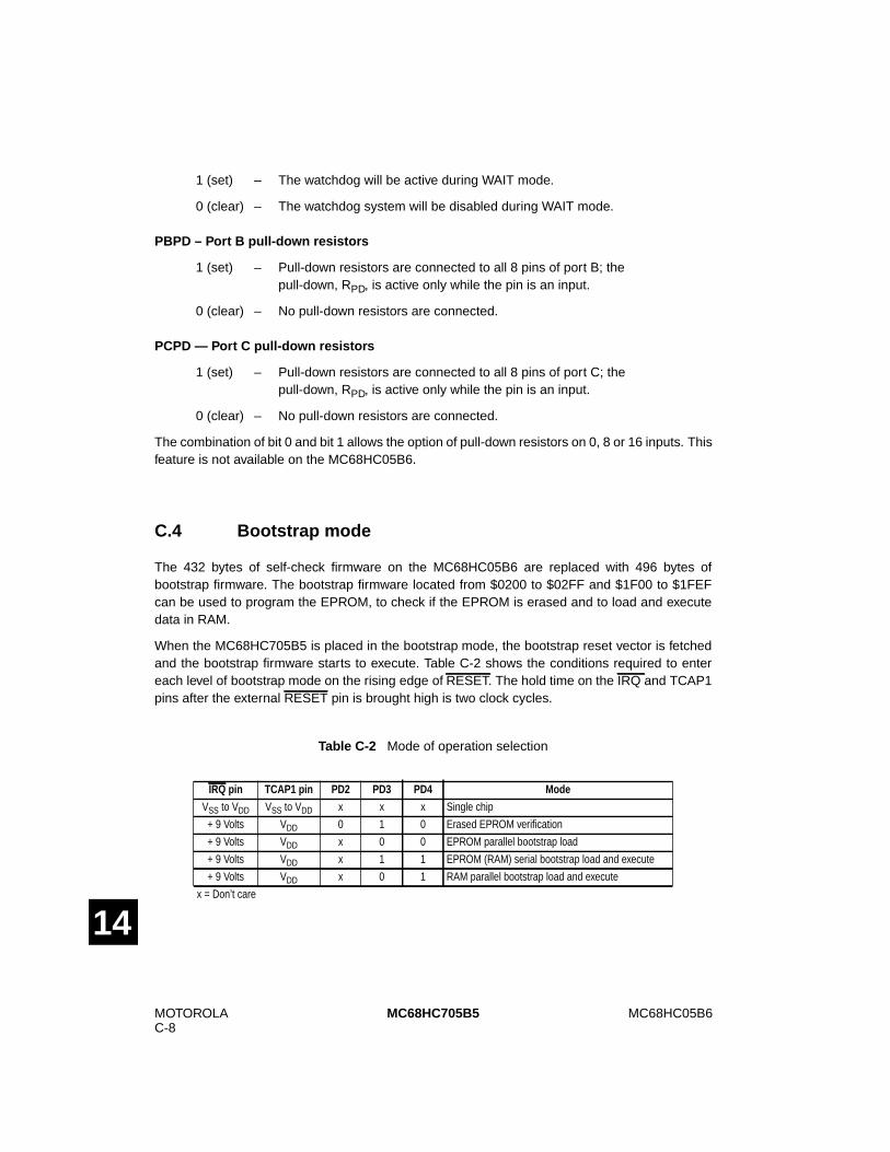
MOTOROLAC-8
MC68HC05B6MC68HC705B5
14
1 (set) – The watchdog will be active during WAIT mode.
0 (clear) – The watchdog system will be disabled during WAIT mode.
PBPD – Port B pull-down resistors
1 (set) – Pull-down resistors are connected to all 8 pins of port B; thepull-down, RPD, is active only while the pin is an input.
0 (clear) – No pull-down resistors are connected.
PCPD — Port C pull-down resistors
1 (set) – Pull-down resistors are connected to all 8 pins of port C; thepull-down, RPD, is active only while the pin is an input.
0 (clear) – No pull-down resistors are connected.
The combination of bit 0 and bit 1 allows the option of pull-down resistors on 0, 8 or 16 inputs. Thisfeature is not available on the MC68HC05B6.
C.4 Bootstrap mode
The 432 bytes of self-check firmware on the MC68HC05B6 are replaced with 496 bytes ofbootstrap firmware. The bootstrap firmware located from $0200 to $02FF and $1F00 to $1FEFcan be used to program the EPROM, to check if the EPROM is erased and to load and executedata in RAM.
When the MC68HC705B5 is placed in the bootstrap mode, the bootstrap reset vector is fetchedand the bootstrap firmware starts to execute. Table C-2 shows the conditions required to entereach level of bootstrap mode on the rising edge of RESET. The hold time on the IRQ and TCAP1pins after the external RESET pin is brought high is two clock cycles.
Table C-2 Mode of operation selection
IRQ pin TCAP1 pin PD2 PD3 PD4 Mode
VSS to VDD VSS to VDD x x x Single chip
+ 9 Volts VDD 0 1 0 Erased EPROM verification
+ 9 Volts VDD x 0 0 EPROM parallel bootstrap load
+ 9 Volts VDD x 1 1 EPROM (RAM) serial bootstrap load and execute
+ 9 Volts VDD x 0 1 RAM parallel bootstrap load and execute
x = Don’t care
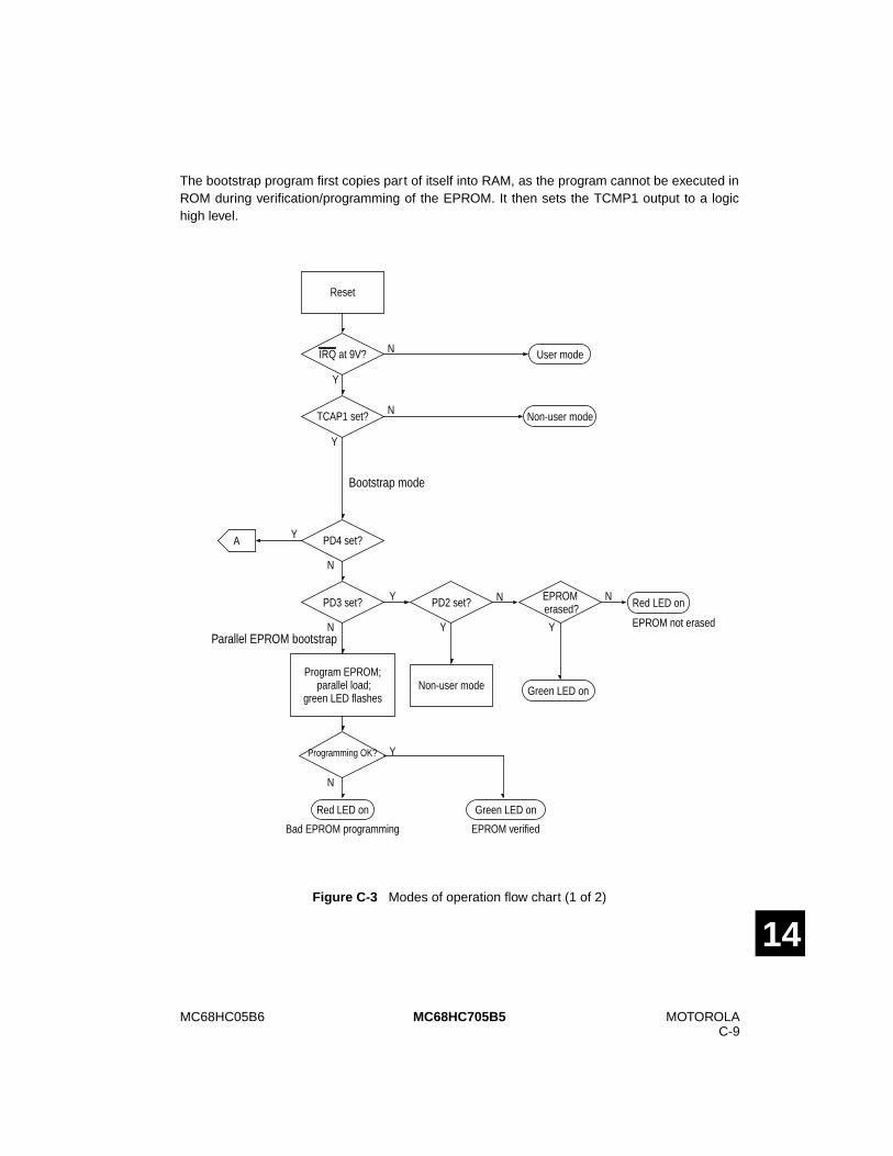
MC68HC05B6 MOTOROLAC-9
MC68HC705B5
14
The bootstrap program first copies part of itself into RAM, as the program cannot be executed inROM during verification/programming of the EPROM. It then sets the TCMP1 output to a logichigh level.
Figure C-3 Modes of operation flow chart (1 of 2)
TCAP1 set?
IRQ at 9V?
EPROM erased?PD2 set?PD3 set?
PD4 set?
Reset
Program EPROM;parallel load;
green LED flashes
Programming OK?
User mode
Red LED on
Green LED onNon-user mode
Red LED on Green LED on
Non-user mode
A
Y
Y
Y
Y
Y Y
N
N
N
N N
N
Y
Bootstrap mode
EPROM not erased
EPROM verified
Parallel EPROM bootstrap
Bad EPROM programming
N
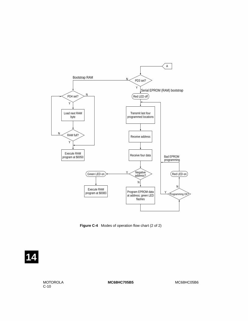
MOTOROLAC-10
MC68HC05B6MC68HC705B5
14
Figure C-4 Modes of operation flow chart (2 of 2)
Programming OK?
Negativeaddress?
PD4 set?
PD3 set?
Transmit last fourprogrammed locations
A
Red LED off
Receive address
Receive four data
Execute RAMprogram at $0083
Green LED on
Load next RAMbyte
RAM full?
Execute RAMprogram at $0050
Program EPROM dataat address; green LED
flashes
Red LED on
N
Y
Y
Y
Y
Y
N
NN
Serial EPROM (RAM) bootstrap
Bad EPROM
Bootstrap RAM
programming
N
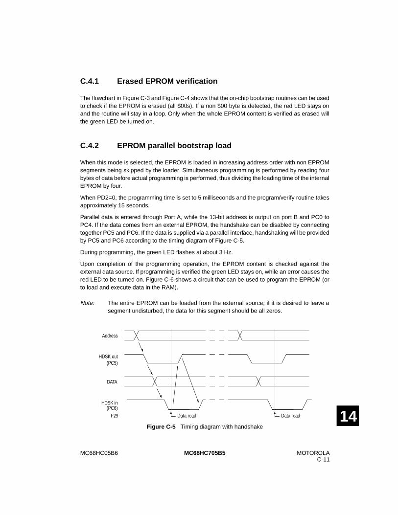
MC68HC05B6 MOTOROLAC-11
MC68HC705B5
14
C.4.1 Erased EPROM verification
The flowchart in Figure C-3 and Figure C-4 shows that the on-chip bootstrap routines can be usedto check if the EPROM is erased (all $00s). If a non $00 byte is detected, the red LED stays onand the routine will stay in a loop. Only when the whole EPROM content is verified as erased willthe green LED be turned on.
C.4.2 EPROM parallel bootstrap load
When this mode is selected, the EPROM is loaded in increasing address order with non EPROMsegments being skipped by the loader. Simultaneous programming is performed by reading fourbytes of data before actual programming is performed, thus dividing the loading time of the internalEPROM by four.
When PD2=0, the programming time is set to 5 milliseconds and the program/verify routine takesapproximately 15 seconds.
Parallel data is entered through Port A, while the 13-bit address is output on port B and PC0 toPC4. If the data comes from an external EPROM, the handshake can be disabled by connectingtogether PC5 and PC6. If the data is supplied via a parallel interface, handshaking will be providedby PC5 and PC6 according to the timing diagram of Figure C-5.
During programming, the green LED flashes at about 3 Hz.
Upon completion of the programming operation, the EPROM content is checked against theexternal data source. If programming is verified the green LED stays on, while an error causes thered LED to be turned on. Figure C-6 shows a circuit that can be used to program the EPROM (orto load and execute data in the RAM).
Note: The entire EPROM can be loaded from the external source; if it is desired to leave asegment undisturbed, the data for this segment should be all zeros.
Figure C-5 Timing diagram with handshake
Data read Data read
Address
HDSK out(PC5)
DATA
HDSK in(PC6)
F29
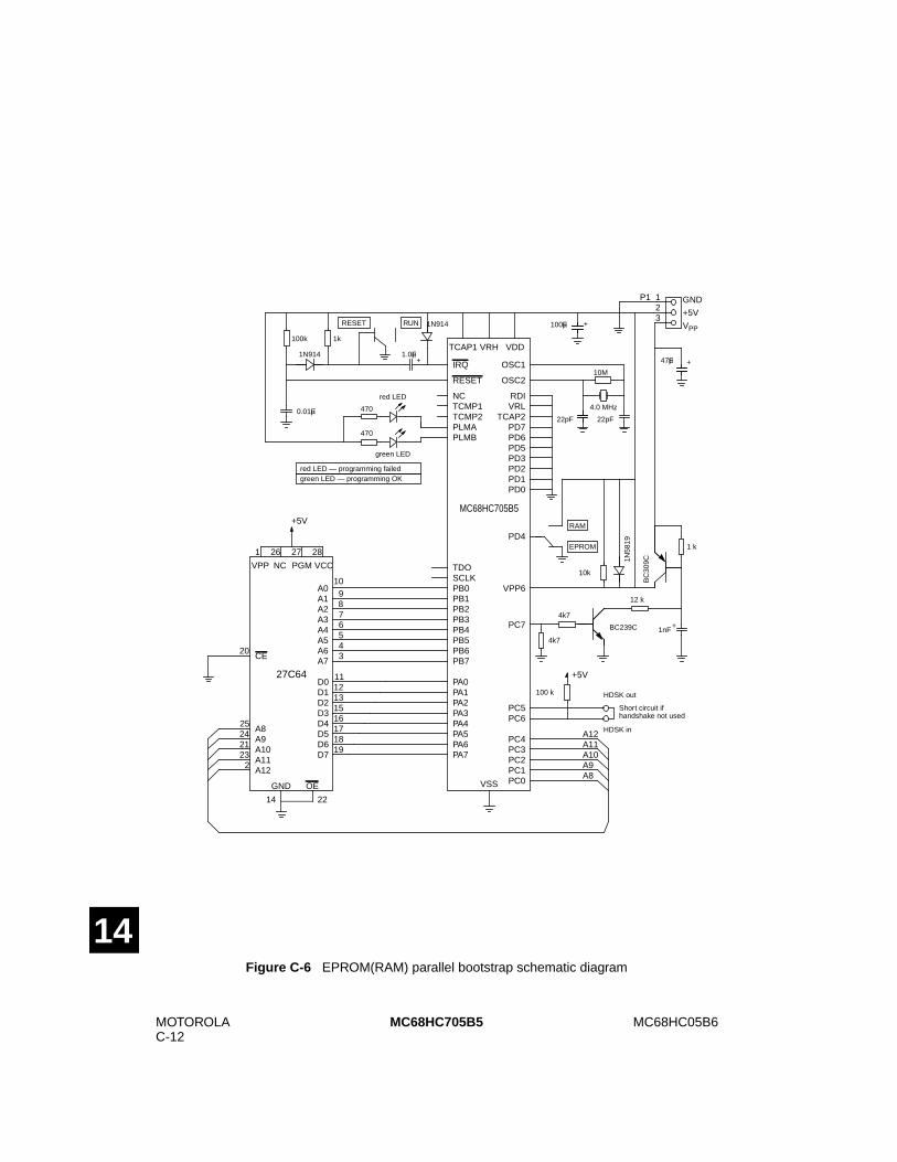
MOTOROLAC-12
MC68HC05B6MC68HC705B5
14Figure C-6 EPROM(RAM) parallel bootstrap schematic diagram
PB0PB1PB2PB3PB4PB5PB6PB7
PA0PA1PA2PA3PA4PA5PA6PA7
VDD
OSC1
OSC2
TCAP1
IRQ
RESET
VSS
A0A1A2A3A4A5A6A7
D0D1D2D3D4D5D6D7
GND OE
VCCPGMVPP
14 22
10987654
1 26 27 28
12131516171819
11
3
+5V
12
P1 GND
+5V100µF
22pF
4.0 MHz
1N914
1k½
1.0µF
22pF
10M½
100k½
1N914
RESET RUN
0.01µF
TDOSCLK
RDIVRL
TCAP2PD7PD6PD5PD3PD2PD1PD0
PD4
+5V
3VPP
VPP6
PC7
PC5
PC4PC3PC2PC1PC0
PC6
NC
242123
2
A9A8
A10
A12
CE
A11
A12A11A10A9A8
HDSK out
HDSK in
Short circuit ifhandshake not used
100 k½
NCTCMP1TCMP2PLMAPLMB
470½
470½
red LED
green LED
4k7½
4k7½
12 k½
BC239C
BC
309C
10k ½
27C64
+
+
VRH
red LED — programming failedgreen LED — programming OK
25
1nF1N
5819
1 k½
+
RAM
EPROM
47µF +
20
MC68HC705B5
MC68HC05B6 MOTOROLAC-13
MC68HC705B5
14
C.4.3 EPROM (RAM) serial bootstrap load and execute
The serial routine communicates through the SCI with an external host, typically a PC, by meansof an RS232 link at 9600 baud, 8-bit, no parity and full duplex.
Data format is not ASCII, but 8-bit binary, so a complementary program must be run by the hostto supply the required format. Such a program is available for the IBM PC from Motorola.
The EPROM bootstrap routines are used to customise the OTP EPROM. To increase the speedof programming, four bytes are programmed in parallel while the data is simultaneouslytransmitted and received in full duplex. This implies that while 4 bytes are being programmed, thenext 4 bytes are received and the preceding 4 bytes are echoed. The format accepted by the serialloader is as follows:
[address n high] [address n low] [data(n)] [data (n+1)] [data (n+2)] [data (n+3)]
Address n must have the two LSBs at zero so that n, n+1, n+2 and n+3 have identical MSBs.These blocks of four bytes do not need to be contiguous, as a new address is transmitted for eachnew group.
The protocol is as follows:
1 The MC68HC705B5 sends the last two bytes programmed to the host as aprompt; this allows verification by the host of proper programming.
2 In response to the first byte prompt, the host sends the first address byte.
3 After receiving the first address byte, the MC68HC705B5 sends the nextbyte programmed.
4 The exchange of data continues until the MC68HC705B5 has sent the fourdata bytes and the host has sent the 2 address data bytes and 4 data bytes.
5 If the data is non zero, it is programmed at the address provided, while thenext address and bytes are received and the previous data is echoed.
6 Loop to 1.
After reset, the MC68HC705B5 serial bootstrap routine will first echo two blocks of four bytes at$0000, as no data is programmed yet.
If the data sent in is $00, no programming in the EPROM takes place, and the contents of theaccessed location are returned as a prompt. The entire EPROM memory can be read in thisfashion (serial dump). The red LED will be on if the data read from the EPROM is not $00.
Serial RAM loading and execute can be accomplished in this mode. A RAM byte will be written ifthe address sent by the host in the serial protocol points to the RAM.
In the RAM bootloader mode, all interrupt vectors are mapped to pseudo-vectors in RAM (seeTable C-3). This allows programmers to use their own service-routine addresses. Eachpseudo-vector is allowed three bytes of space rather than the two bytes for normal vectors,because an explicit jump (JMP) opcode is needed to cause the desired jump to the user’sservice-routine address.
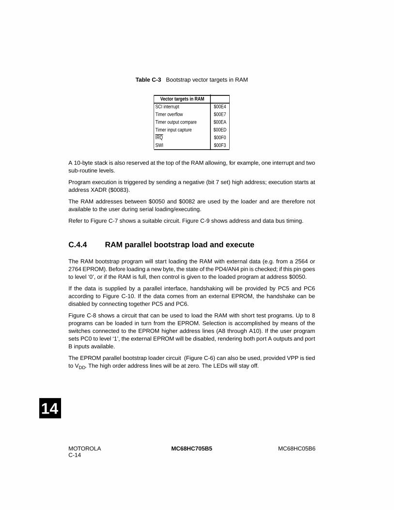
MOTOROLAC-14
MC68HC05B6MC68HC705B5
14
A 10-byte stack is also reserved at the top of the RAM allowing, for example, one interrupt and twosub-routine levels.
Program execution is triggered by sending a negative (bit 7 set) high address; execution starts ataddress XADR ($0083).
The RAM addresses between $0050 and $0082 are used by the loader and are therefore notavailable to the user during serial loading/executing.
Refer to Figure C-7 shows a suitable circuit. Figure C-9 shows address and data bus timing.
C.4.4 RAM parallel bootstrap load and execute
The RAM bootstrap program will start loading the RAM with external data (e.g. from a 2564 or2764 EPROM). Before loading a new byte, the state of the PD4/AN4 pin is checked; if this pin goesto level ‘0’, or if the RAM is full, then control is given to the loaded program at address $0050.
If the data is supplied by a parallel interface, handshaking will be provided by PC5 and PC6according to Figure C-10. If the data comes from an external EPROM, the handshake can bedisabled by connecting together PC5 and PC6.
Figure C-8 shows a circuit that can be used to load the RAM with short test programs. Up to 8programs can be loaded in turn from the EPROM. Selection is accomplished by means of theswitches connected to the EPROM higher address lines (A8 through A10). If the user programsets PC0 to level ‘1’, the external EPROM will be disabled, rendering both port A outputs and portB inputs available.
The EPROM parallel bootstrap loader circuit (Figure C-6) can also be used, provided VPP is tiedto VDD. The high order address lines will be at zero. The LEDs will stay off.
Table C-3 Bootstrap vector targets in RAM
Vector targets in RAM
SCI interrupt $00E4
Timer overflow $00E7
Timer output compare $00EA
Timer input capture $00ED
IRQ $00F0
SWI $00F3
MC68HC05B6 MOTOROLAC-15
MC68HC705B5
14Figure C-7 EPROM (RAM) serial bootstrap schematic diagram
Red — programming errorGreen — programming OK
40
VPP6
PC7
PB0PB1PB2PB3PB4PB5PB6PB7
PA0PA1PA2PA3PA4PA5PA6PA7
VDD
OSC1
OSC2
TCAP1
IRQ
RESET
VSS
12
P1 GND
+5V
1N9141k½
1.0µF
100k½
1N914
RESET RUN
0.01µF
3VPP
PC5PC4PC3PC2PC1PC0
PC6
PLMA
PLMB
470½
470½
Red LED
Green LED
+
+
VRH
22µF
22µF
22µF
2 x 3K½ 12
34
8
675
111213
14
15
16
5321
22µF
RS232Connector
MAX232
+5V9600 BD
8-bitno parity
19
18
20
21
5052
3938373635343332
3130292827262524
1413125
43444546474849
232151
22 8 10
41 7
VRL
TCAP2TCMP1TCMP2
SCLKNC
10nF47µF
PD0
PD4
PD1PD2PD5PD6PD7
+
+
+
+
22pF
4.0 MHz
22pF
10M½
4k7½
4k7½
12 k½
BC239C
BC
309C
10k ½
1nF1N
5819
1 k½
+
Serial boot
Erase check
47µF +
PD3
4
RDITDO
Erase check
Red — EPROM not erasedGreen — EPROM erased
Serial boot
MC68HC705B5
3
MOTOROLAC-16
MC68HC05B6MC68HC705B5
14Figure C-8 RAM parallel bootstrap schematic diagram
PB0PB1PB2PB3PB4PB5PB6PB6PB7
PA0PA1PA2PA3PA4PA5PA6PA7
VDD
TCAP2TCMP2TCMP1
PLMBPLMASCLKTDORDI
VRHVRLPD7PD6PD5PD3PD2PD1PD0PC7PC6PC5PC4PC3PC2PC1PC0
NC
OSC1
OSC2
TCAP1
IRQ
RESET
PD4VPP6
VSS
A0A1A2A3A4A5A6A7
D0D1D2D3D4D5D6D7
GND OE
A8
A9
A10
A11A12
CE
VCCPGMVPP
20
2
25
24
23
14 22
10987654
1 26 27 28
21
12131516171819
11
3
+5V
3 x 4.7k½
+5V+5V
16 x 100k½
1
2
P1 GND
+5V100µF
22pF
4.0 MHz
1N914
1k½
1.0µF
22pF
10M½
100k½
1N914
RESET RUN
0.01µF
U12764
+5V18 x 100 k½
+
+
NC
MC68HC705B5
MC68HC05B6 MOTOROLAC-17
MC68HC705B5
14
C.4.5 Bootstrap loader timing diagrams
Figure C-9 EPROM parallel bootstrap loader timing diagram
tCOOE
tADEtDHE
Address
Data
tADEtDHE
tADEtDHE
tADEtDHE
tCOOE tCOOE tCDDE
tADE max (address to data delay) 5 machine cycles
tDHA min (data hold time) 14 machine cycles
tCOOE (load cycle time) 117 machine cycles < tCOOE < 150 machine cycles
tCDDE (programming cycle time) tCOOE + tPROG (5ms nominal)
1 machine cycle = 1/(2f0(Xtal))
MOTOROLAC-18
MC68HC05B6MC68HC705B5
14
Figure C-10 RAM parallel loader timing diagram
tADR tDHR
Address
Data
tCR
PD4 tEXR max
tHO
tHI max
PC5 out
PC6 in
tADR max (address to data delay; PC6=PC5) 16 machine cycles
tDHR min (data hold time) 4 machine cycles
tCR (load cycle time; PC6=PC5) 49 machine cycles
tHO (PC5 handshake out delay) 5 machine cycles
tHI max (PC6 handshake in, data hold time) 10 machine cycles
tEXR max (max delay for transition to berecognised during this cycle; PC6=PC5 30 machine cycles
1 machine cycle = 1/(2f0(Xtal))
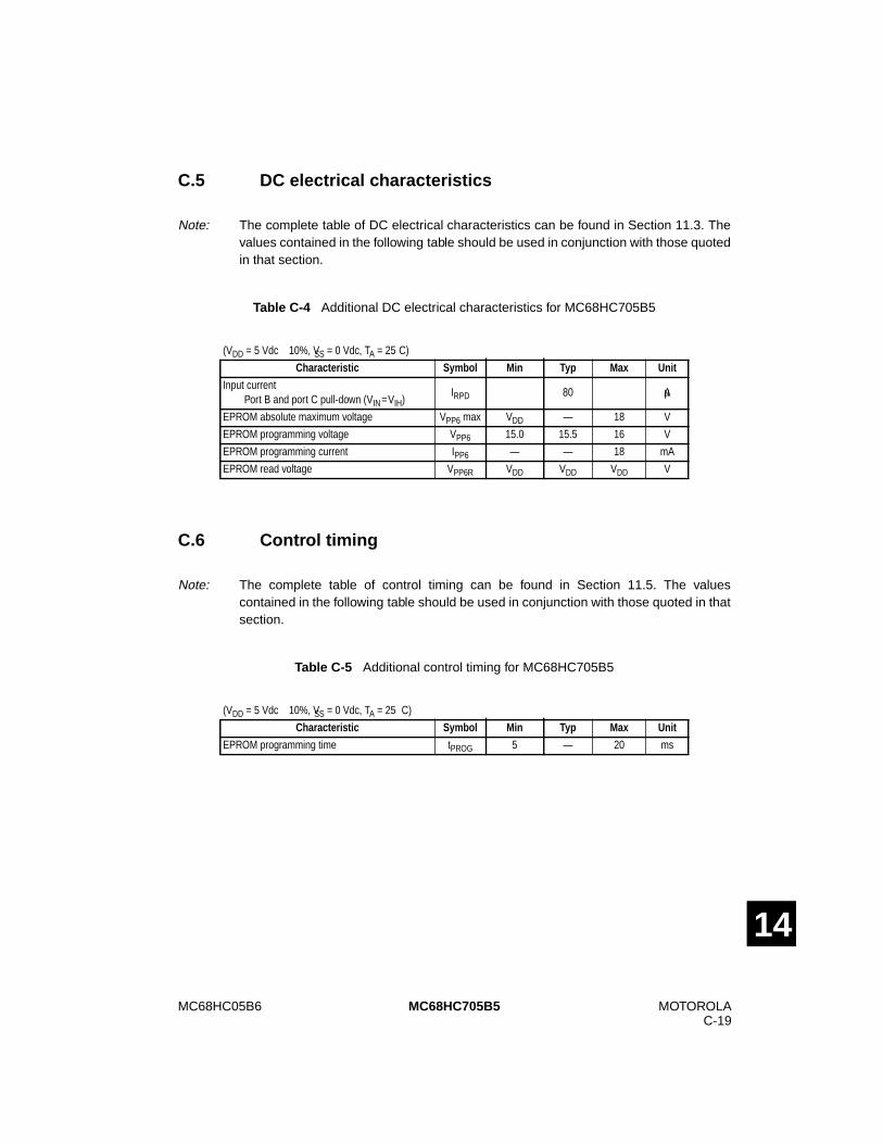
MC68HC05B6 MOTOROLAC-19
MC68HC705B5
14
C.5 DC electrical characteristics
Note: The complete table of DC electrical characteristics can be found in Section 11.3. Thevalues contained in the following table should be used in conjunction with those quotedin that section.
C.6 Control timing
Note: The complete table of control timing can be found in Section 11.5. The valuescontained in the following table should be used in conjunction with those quoted in thatsection.
Table C-4 Additional DC electrical characteristics for MC68HC705B5
(VDD = 5 Vdc ± 10%, VSS = 0 Vdc, TA = 25¡C)
Characteristic Symbol Min Typ Max Unit
Input currentPort B and port C pull-down (VIN=VIH)
IRPD 80 µA
EPROM absolute maximum voltage VPP6 max VDD — 18 V
EPROM programming voltage VPP6 15.0 15.5 16 V
EPROM programming current IPP6 — — 18 mA
EPROM read voltage VPP6R VDD VDD VDD V
Table C-5 Additional control timing for MC68HC705B5
(VDD = 5 Vdc ± 10%, VSS = 0 Vdc, TA = 25¡ C)
Characteristic Symbol Min Typ Max Unit
EPROM programming time tPROG 5 — 20 ms

MOTOROLAC-20
MC68HC05B6MC68HC705B5
THIS PAGE INTENTIONALLY LEFT BLANK
14
MC68HC05B6 MOTOROLAD-1
MC68HC05B16
14
DMC68HC05B16
The MC68HC05B16 is a device similar to the MC68HC05B6, but with increased RAM, ROM andself-check ROM sizes. The entire MC68HC05B6 data sheet, including the electricalcharacteristics, applies to the MC68HC05B16, with the exceptions outlined in this appendix.
Features
• 15 kbytes User ROM
• 352 bytes of RAM
• 496 bytes self-check ROM
• 52-pin PLCC, 56-pin SDIP and 64-pin QFP packages
D.1 Self-check routines
The self-check routines for the MC68HC05B16 are identical to those of the MC68HC05B6 withthe following exception.
The count byte on the MC68HC05B16 can be any value up to 256 ($00). The first 176 bytes areloaded into RAM I and the remainder is loaded into RAM II starting at $0250.

MOTOROLAD-2
MC68HC05B16MC68HC05B16
14
Figure D-1 MC68HC05B16 block diagram
Port
A
PA0PA1PA2PA3PA4PA5PA6PA7
Port
B
PB0PB1PB2PB3PB4PB5PB6PB7
Port
C
PC0PC1PC2/ECLKPC3PC4PC5PC6PC7
16-bittimer
Port
D
PD0/AN0PD1/AN1PD2/AN2PD3/AN3PD4/AN4PD5/AN5PD6/AN6PD7/AN7
Oscillator
COP watchdogRESET
IRQ
VDDVSS
OSC1OSC2
M68HC05CPU
SCIA/D converter
PLM
TCAP1TCAP2
TCMP1TCMP2
VRHVRL
RDISCLKTDO
VPP1
256 bytesEEPROM
Charge pump
2 / 32
PLMA D/APLMB D/A
8-bit
15120 bytesROM
352 bytesstatic RAM
496 bytesself-check ROM
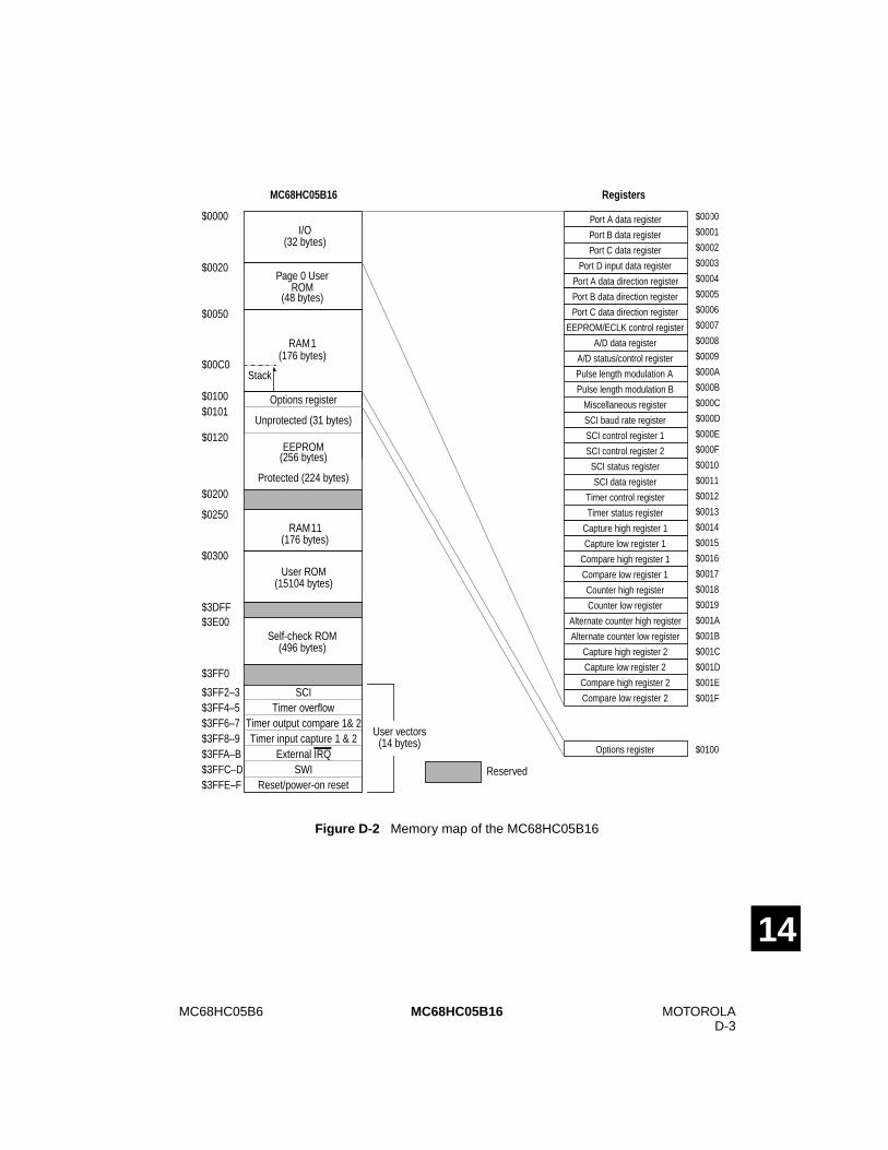
MC68HC05B6 MOTOROLAD-3
MC68HC05B16
14
Figure D-2 Memory map of the MC68HC05B16
Port B data register
Port C data register
Port D input data register
Port A data register $0000
Compare low register 2
A/D data register
$0000I/O
(32 bytes)
$0020
$00C0
$0100
$3FF0
Stack
RAM1(176 bytes)
$0250
$0200
$3E00
$0050
Port A data direction register
Port B data direction register
Port C data direction register
EEPROM/ECLK control register
A/D status/control register
Pulse length modulation A
Pulse length modulation B
Miscellaneous register
SCI baud rate register
SCI control register 1
SCI control register 2
SCI status register
SCI data register
Timer control register
Timer status register
Capture high register 1
Capture low register 1
Compare high register 1
Compare low register 1
Counter high register
Counter low register
Alternate counter high register
Alternate counter low register
Capture high register 2
Capture low register 2
Compare high register 2
$0001
$0002
$0003
$0004
$0005
$0006
$0007
$0008
$0009
$000A
$000B
$000C
$000D
$000E
$000F
$0010
$0011
$0012
$0013
$0014
$0015
$0016
$0017
$0018
$0019
$001A
$001B
$001C
$001D
$001E
$001F
Page 0 UserROM
(48 bytes)
User ROM(15104 bytes)
Self-check ROM(496 bytes)
$0300
Options register
Unprotected (31 bytes)
Protected (224 bytes)
EEPROM(256 bytes)
$0101
$0120
$0100Options register
Reserved
MC68HC05B16 Registers
RAM11(176 bytes)
$3DFF
User vectors(14 bytes)
$3FF2–3 SCITimer overflow
Timer output compare 1& 2Timer input capture 1 & 2
External IRQSWI
Reset/power-on reset
$3FF4–5$3FF6–7$3FF8–9$3FFA–B$3FFC–D$3FFE–F
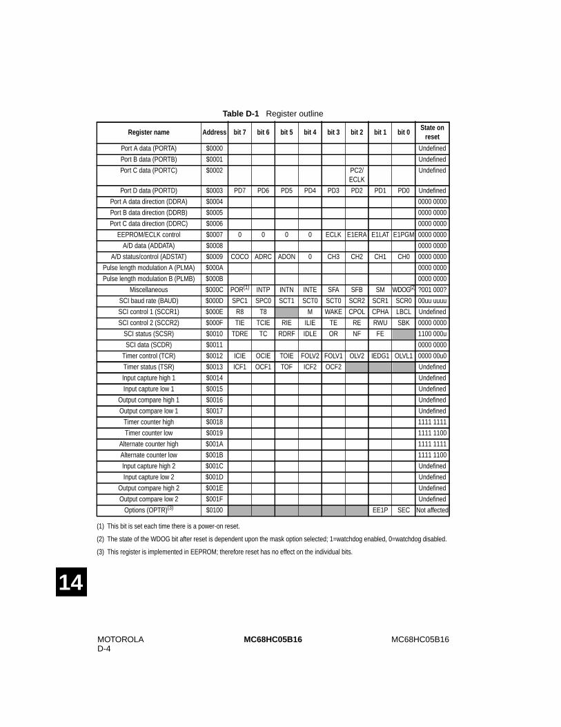
MOTOROLAD-4
MC68HC05B16MC68HC05B16
14
(1) This bit is set each time there is a power-on reset.
(2) The state of the WDOG bit after reset is dependent upon the mask option selected; 1=watchdog enabled, 0=watchdog disabled.
(3) This register is implemented in EEPROM; therefore reset has no effect on the individual bits.
Table D-1 Register outline
Register name Address bit 7 bit 6 bit 5 bit 4 bit 3 bit 2 bit 1 bit 0State on
reset
Port A data (PORTA) $0000 Undefined
Port B data (PORTB) $0001 Undefined
Port C data (PORTC) $0002 PC2/ECLK
Undefined
Port D data (PORTD) $0003 PD7 PD6 PD5 PD4 PD3 PD2 PD1 PD0 Undefined
Port A data direction (DDRA) $0004 0000 0000
Port B data direction (DDRB) $0005 0000 0000
Port C data direction (DDRC) $0006 0000 0000
EEPROM/ECLK control $0007 0 0 0 0 ECLK E1ERA E1LAT E1PGM 0000 0000
A/D data (ADDATA) $0008 0000 0000
A/D status/control (ADSTAT) $0009 COCO ADRC ADON 0 CH3 CH2 CH1 CH0 0000 0000
Pulse length modulation A (PLMA) $000A 0000 0000
Pulse length modulation B (PLMB) $000B 0000 0000
Miscellaneous $000C POR(1) INTP INTN INTE SFA SFB SM WDOG(2) ?001 000?
SCI baud rate (BAUD) $000D SPC1 SPC0 SCT1 SCT0 SCT0 SCR2 SCR1 SCR0 00uu uuuu
SCI control 1 (SCCR1) $000E R8 T8 M WAKE CPOL CPHA LBCL Undefined
SCI control 2 (SCCR2) $000F TIE TCIE RIE ILIE TE RE RWU SBK 0000 0000
SCI status (SCSR) $0010 TDRE TC RDRF IDLE OR NF FE 1100 000u
SCI data (SCDR) $0011 0000 0000
Timer control (TCR) $0012 ICIE OCIE TOIE FOLV2 FOLV1 OLV2 IEDG1 OLVL1 0000 00u0
Timer status (TSR) $0013 ICF1 OCF1 TOF ICF2 OCF2 Undefined
Input capture high 1 $0014 Undefined
Input capture low 1 $0015 Undefined
Output compare high 1 $0016 Undefined
Output compare low 1 $0017 Undefined
Timer counter high $0018 1111 1111
Timer counter low $0019 1111 1100
Alternate counter high $001A 1111 1111
Alternate counter low $001B 1111 1100
Input capture high 2 $001C Undefined
Input capture low 2 $001D Undefined
Output compare high 2 $001E Undefined
Output compare low 2 $001F Undefined
Options (OPTR)(3) $0100 EE1P SEC Not affected
MC68HC05B6 MOTOROLAE-1
MC68HC705B16
14
EMC68HC705B16
The MC68HC705B16 is a device similar to the MC68HC05B6, but with increased RAM and15 kbytes of EPROM instead of 6 kbytes of ROM. In addition, the self-check routines available inthe MC68HC05B6 are replaced by bootstrap firmware. The MC68HC705B16 is an OTPROM(one-time programmable ROM) version of the MC68HC05B16, meaning that once the applicationprogram has been loaded in the EPROM it can never be erased. The entire MC68HC05B6 datasheet applies to the MC68HC705B16, with the exceptions outlined in this appendix.
Features
• 15 kbytes EPROM
• 352 bytes of RAM
• 576 bytes bootstrap ROM
• Simultaneous programming of up to 8 bytes of EPROM
• Optional pull-down resistors available on all port B and port C pins
• 52-pin PLCC and 64-pin QFP packages
Note: The electrical characteristics of the MC68HC05B6 as provided in Section 11 do notapply to the MC68HC705B16. Data specific to the MC68HC705B16 can be found inthis appendix.
To ensure correct operation of the MC68HC705B16 after power-on, the device mustbe reset a second time after power-on. This can be done in software using theMC68HC705B16 watchdog.
The following software sub-routine should be used:RESET2 BSET 0, $0C Start watchdog
STOP STOP causes immediate watchdogsystem reset
The interrupt vector at $3FF0 and $3FF1 must be initialised with the RESET2 addressvalue.
MOTOROLAE-2
MC68HC705B16MC68HC705B16
14
Figure E-1 MC68HC705B16 block diagram
Port
A
PA0PA1PA2PA3PA4PA5PA6PA7
Port
B
PB0PB1PB2PB3PB4PB5PB6PB7
Port
C
PC0PC1PC2/ECLKPC3PC4PC5PC6PC7
16-bittimer
Port
D
PD0/AN0PD1/AN1PD2/AN2PD3/AN3PD4/AN4PD5/AN5PD6/AN6PD7/AN7
Oscillator
COP watchdogRESET
IRQ
VDDVSS
OSC1OSC2
M68HC05CPU
SCIA/D converter
PLM
TCAP1TCAP2
TCMP1TCMP2
VRHVRL
RDISCLKTDO
VPP1
256 bytesEEPROM
Charge pump
2 / 32
PLMA D/APLMB D/A
8-bit
15168 bytesEPROM
352 bytesstatic RAM
576 bytes
VPP6
bootstrap ROM
MC68HC05B6 MOTOROLAE-3
MC68HC705B16
14
Figure E-2 Memory map of the MC68HC705B16
Port B data register
Port C data register
Port D input data register
Port A data register $0000
Compare low register 2
A/D data register
$0000I/O
(32 bytes)
$0020
$00C0
$0100
$3FF0
Stack
RAM1(176 bytes)
$0250
$0200
$3E00
$0050
Port A data direction register
Port B data direction register
Port C data direction register
E/EEPROM/ECLK control register
A/D status/control register
Pulse length modulation A
Pulse length modulation B
Miscellaneous register
SCI baud rate register
SCI control register 1
SCI control register 2
SCI status register
SCI data register
Timer control register
Timer status register
Capture high register 1
Capture low register 1
Compare high register 1
Compare low register 1
Counter high register
Counter low register
Alternate counter high register
Alternate counter low register
Capture high register 2
Capture low register 2
Compare high register 2
$0001
$0002
$0003
$0004
$0005
$0006
$0007
$0008
$0009
$000A
$000B
$000C
$000D
$000E
$000F
$0010
$0011
$0012
$0013
$0014
$0015
$0016
$0017
$0018
$0019
$001A
$001B
$001C
$001D
$001E
$001F
Page 0 UserEPROM
(48 bytes)
User EPROM(15104 bytes)
Bootstrap ROM11(496 bytes)
$0300
Options register
Unprotected (31 bytes)
Protected (224 bytes)
EEPROM(256 bytes)
$0101
$0120
$0100Options register
Reserved
MC68HC705B16 Registers
RAM11(176 bytes)
$3DFE$3DFF
Mask option register
Mask option register $3DFE
Bootstrap ROM1(80 bytes)
User vectors(14 bytes)
$3FF2–3 SCITimer overflow
Timer output compare 1& 2Timer input capture 1 & 2
External IRQSWI
Reset/power-on reset
$3FF4–5$3FF6–7$3FF8–9$3FFA–B$3FFC–D$3FFE–F

MOTOROLAE-4
MC68HC705B16MC68HC705B16
14
(1) This bit is set each time there is a power-on reset.
(2) The state of the WDOG bit after reset is dependent upon the mask option selected; 1=watchdog enabled, 0=watchdog disabled.
(3) This register is implemented in EEPROM; therefore reset has no effect on the individual bits.
(4) This register is implemented in EPROM; therefore reset has no effect on the individual bits.
Table E-1 Register outline
Register name Address bit 7 bit 6 bit 5 bit 4 bit 3 bit 2 bit 1 bit 0State on
reset
Port A data (PORTA) $0000 Undefined
Port B data (PORTB) $0001 Undefined
Port C data (PORTC) $0002 PC2/ECLK
Undefined
Port D data (PORTD) $0003 PD7 PD6 PD5 PD4 PD3 PD2 PD1 PD0 Undefined
Port A data direction (DDRA) $0004 0000 0000
Port B data direction (DDRB) $0005 0000 0000
Port C data direction (DDRC) $0006 0000 0000
EPROM/EEPROM/ECLK control $0007 E6LAT E6PGM ECLK E1ERA E1LAT E1PGM 0000 0000
A/D data (ADDATA) $0008 0000 0000
A/D status/control (ADSTAT) $0009 COCO ADRC ADON 0 CH3 CH2 CH1 CH0 0000 0000
Pulse length modulation A (PLMA) $000A 0000 0000
Pulse length modulation B (PLMB) $000B 0000 0000
Miscellaneous $000C POR(1) INTP INTN INTE SFA SFB SM WDOG(2) ?001 000?
SCI baud rate (BAUD) $000D SPC1 SPC0 SCT1 SCT0 SCT0 SCR2 SCR1 SCR0 00uu uuuu
SCI control 1 (SCCR1) $000E R8 T8 M WAKE CPOL CPHA LBCL Undefined
SCI control 2 (SCCR2) $000F TIE TCIE RIE ILIE TE RE RWU SBK 0000 0000
SCI status (SCSR) $0010 TDRE TC RDRF IDLE OR NF FE 1100 000u
SCI data (SCDR) $0011 0000 0000
Timer control (TCR) $0012 ICIE OCIE TOIE FOLV2 FOLV1 OLV2 IEDG1 OLVL1 0000 00u0
Timer status (TSR) $0013 ICF1 OCF1 TOF ICF2 OCF2 Undefined
Input capture high 1 $0014 Undefined
Input capture low 1 $0015 Undefined
Output compare high 1 $0016 Undefined
Output compare low 1 $0017 Undefined
Timer counter high $0018 1111 1111
Timer counter low $0019 1111 1100
Alternate counter high $001A 1111 1111
Alternate counter low $001B 1111 1100
Input capture high 2 $001C Undefined
Input capture low 2 $001D Undefined
Output compare high 2 $001E Undefined
Output compare low 2 $001F Undefined
Options (OPTR)(3) $0100 EE1P SEC Not affected
Mask option register (MOR)(4) $3DFE RTIM RWAT WWAT PBPD PCPD Not affected
MC68HC05B6 MOTOROLAE-5
MC68HC705B16
14
E.1 EPROM
The MC68HC705B16 memory map is given in Figure E-2. The device has a total of 15168 bytesof EPROM (including 14 bytes for User vectors) and 256 bytes of EEPROM.
The EPROM array is supplied by the VPP6 pin in both read and program modes. Typically theuser’s software would be loaded into a programming board where VPP6 is controlled by one of thebootstrap loader routines. It would then be placed in an application where no programming occurs.In this case the VPP6 pin should be hardwired to VDD.
Warning: A minimum VDD voltage must be applied to the VPP6 pin at all times, includingpower-on. Failure to do so could result in permanent damage to the device.
E.1.1 EPROM read operation
The execution of a program in the EPROM address range or a load from the EPROM are bothread operations. The E6LAT bit in the EPROM/EEPROM control register should be cleared to ‘0’which automatically resets the E6PGM bit. In this way the EPROM is read like a normal ROM.Reading the EPROM with the E6LAT bit set will give data that does not correspond to the actualmemory content. As interrupt vectors are in EPROM, they will not be loaded when E6LAT is set.Similarly, the bootstrap ROM routines cannot be executed when E6LAT is set. In read mode, theVPP6 pin must be at the VDD level. When entering the STOP mode, the EPROM is automaticallyset to the read mode.
Note: An erased byte reads as $00.
E.1.2 EPROM program operation
Typically the EPROM will be programmed by the bootstrap routines resident in the on-chip ROM.However, the user program can be used to program some EPROM locations if the properprocedure is followed. In particular, the programming sequence must be running in RAM, as theEPROM will not be available for code execution while the E6LAT bit is set. The VPP6 switchingmust occur externally after the E6PGM bit is set, for example under control of a signal generatedon a pin by the programming routine.
Note: When the part becomes a PROM, only the cumulative programming of bits to logic ‘1’is possible if multiple programming is made on the same byte.
To allow simultaneous programming of up to eight bytes, these bytes must be in the same groupof addresses which share the same most significant address bits; only the three least significantbits can change.
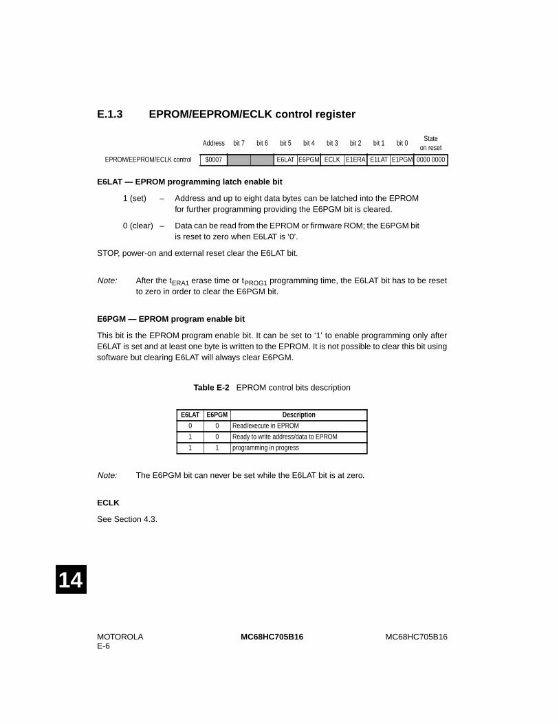
MOTOROLAE-6
MC68HC705B16MC68HC705B16
14
E.1.3 EPROM/EEPROM/ECLK control register
E6LAT — EPROM programming latch enable bit
1 (set) – Address and up to eight data bytes can be latched into the EPROMfor further programming providing the E6PGM bit is cleared.
0 (clear) – Data can be read from the EPROM or firmware ROM; the E6PGM bitis reset to zero when E6LAT is ‘0’.
STOP, power-on and external reset clear the E6LAT bit.
Note: After the tERA1 erase time or tPROG1 programming time, the E6LAT bit has to be resetto zero in order to clear the E6PGM bit.
E6PGM — EPROM program enable bit
This bit is the EPROM program enable bit. It can be set to ‘1’ to enable programming only afterE6LAT is set and at least one byte is written to the EPROM. It is not possible to clear this bit usingsoftware but clearing E6LAT will always clear E6PGM.
Note: The E6PGM bit can never be set while the E6LAT bit is at zero.
ECLK
See Section 4.3.
Address bit 7 bit 6 bit 5 bit 4 bit 3 bit 2 bit 1 bit 0State
on reset
EPROM/EEPROM/ECLK control $0007 E6LAT E6PGM ECLK E1ERA E1LAT E1PGM 0000 0000
Table E-2 EPROM control bits description
E6LAT E6PGM Description
0 0 Read/execute in EPROM
1 0 Ready to write address/data to EPROM
1 1 programming in progress

MC68HC05B6 MOTOROLAE-7
MC68HC705B16
14
E1ERA — EEPROM erase/programming bit
Providing the E1LAT and E1PGM bits are at logic one, this bit indicates whether the access to theEEPROM is for erasing or programming purposes.
1 (set) – An erase operation will take place.
0 (clear) – A programming operation will take place.
Once the program/erase EEPROM address has been selected, E1ERA cannot be changed.
E1LAT — EEPROM programming latch enable bit
1 (set) – Address and data can be latched into the EEPROM for furtherprogram or erase operations, providing the E1PGM bit is cleared.
0 (clear) – Data can be read from the EEPROM. The E1ERA bit and theE1PGM bit are reset to zero when E1LAT is ‘0’.
STOP, power-on and external reset clear the E1LAT bit.
Note: After the tERA1 erase time or tPROG1 programming time, the E1LAT bit has to be resetto zero in order to clear the E1ERA bit and the E1PGM bit.
E1PGM — EEPROM charge pump enable/disable
1 (set) – Internal charge pump generator switched on.
0 (clear) – Internal charge pump generator switched off.
When the charge pump generator is on, the resulting high voltage is applied to the EEPROM array.This bit cannot be set before the data is selected, and once this bit has been set it can only becleared by clearing the E1LAT bit.
A summary of the effects of setting/clearing bits 0, 1 and 2 of the control register are given in Table E-3.
Note: The E1PGM and E1ERA bits are cleared when the E1LAT bit is at zero.
Table E-3 EEPROM control bits description
E1ERA E1LAT E1PGM Description
0 0 0 Read condition
0 1 0 Ready to load address/data for program/erase
0 1 1 Byte programming in progress
1 1 0 Ready for byte erase (load address)
1 1 1 Byte erase in progress
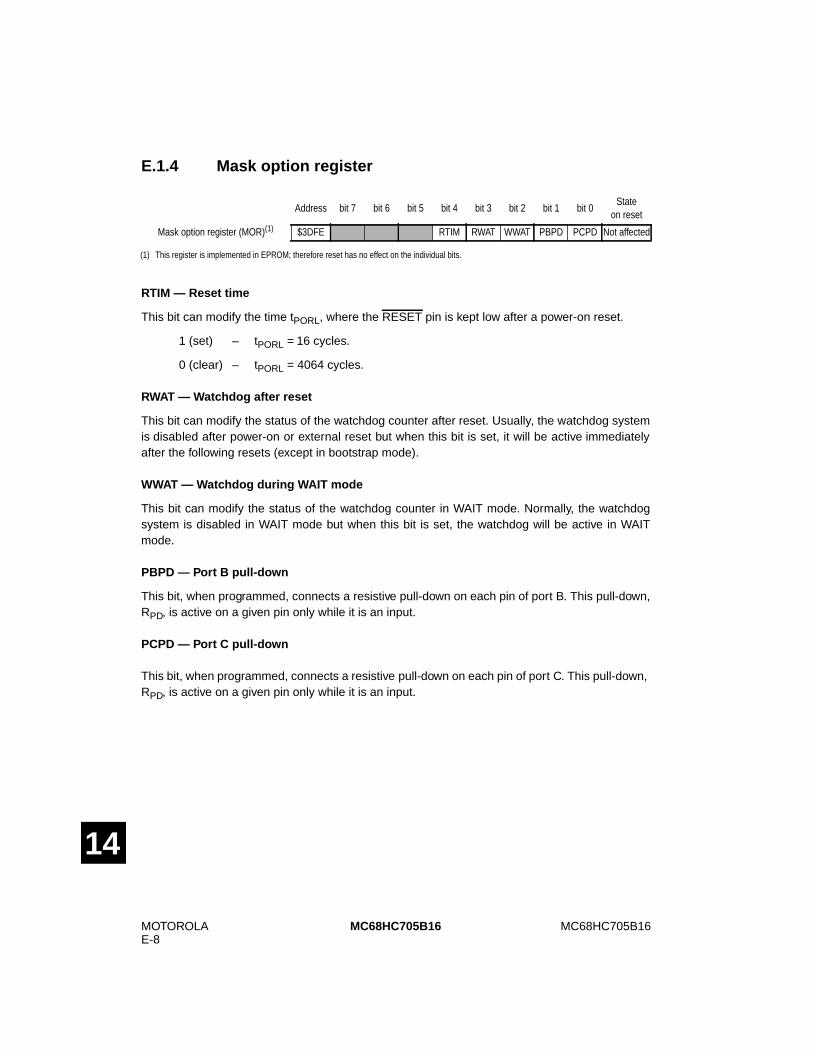
MOTOROLAE-8
MC68HC705B16MC68HC705B16
14
E.1.4 Mask option register
RTIM — Reset time
This bit can modify the time tPORL, where the RESET pin is kept low after a power-on reset.
1 (set) – tPORL = 16 cycles.
0 (clear) – tPORL = 4064 cycles.
RWAT — Watchdog after reset
This bit can modify the status of the watchdog counter after reset. Usually, the watchdog systemis disabled after power-on or external reset but when this bit is set, it will be active immediatelyafter the following resets (except in bootstrap mode).
WWAT — Watchdog during WAIT mode
This bit can modify the status of the watchdog counter in WAIT mode. Normally, the watchdogsystem is disabled in WAIT mode but when this bit is set, the watchdog will be active in WAITmode.
PBPD — Port B pull-down
This bit, when programmed, connects a resistive pull-down on each pin of port B. This pull-down,RPD, is active on a given pin only while it is an input.
PCPD — Port C pull-down
This bit, when programmed, connects a resistive pull-down on each pin of port C. This pull-down,RPD, is active on a given pin only while it is an input.
(1) This register is implemented in EPROM; therefore reset has no effect on the individual bits.
Address bit 7 bit 6 bit 5 bit 4 bit 3 bit 2 bit 1 bit 0State
on reset
Mask option register (MOR)(1) $3DFE RTIM RWAT WWAT PBPD PCPD Not affected
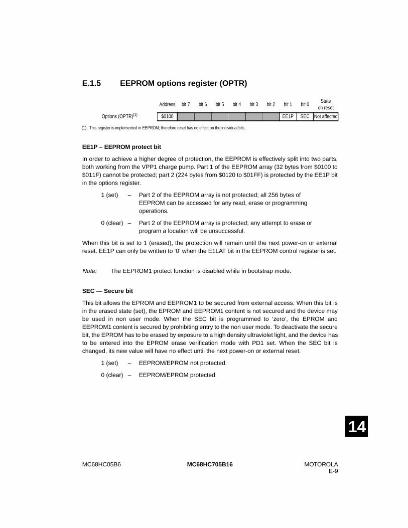
MC68HC05B6 MOTOROLAE-9
MC68HC705B16
14
E.1.5 EEPROM options register (OPTR)
EE1P – EEPROM protect bit
In order to achieve a higher degree of protection, the EEPROM is effectively split into two parts,both working from the VPP1 charge pump. Part 1 of the EEPROM array (32 bytes from $0100 to$011F) cannot be protected; part 2 (224 bytes from $0120 to $01FF) is protected by the EE1P bitin the options register.
1 (set) – Part 2 of the EEPROM array is not protected; all 256 bytes ofEEPROM can be accessed for any read, erase or programmingoperations.
0 (clear) – Part 2 of the EEPROM array is protected; any attempt to erase orprogram a location will be unsuccessful.
When this bit is set to 1 (erased), the protection will remain until the next power-on or externalreset. EE1P can only be written to ‘0’ when the E1LAT bit in the EEPROM control register is set.
Note: The EEPROM1 protect function is disabled while in bootstrap mode.
SEC — Secure bit
This bit allows the EPROM and EEPROM1 to be secured from external access. When this bit isin the erased state (set), the EPROM and EEPROM1 content is not secured and the device maybe used in non user mode. When the SEC bit is programmed to ‘zero’, the EPROM andEEPROM1 content is secured by prohibiting entry to the non user mode. To deactivate the securebit, the EPROM has to be erased by exposure to a high density ultraviolet light, and the device hasto be entered into the EPROM erase verification mode with PD1 set. When the SEC bit ischanged, its new value will have no effect until the next power-on or external reset.
1 (set) – EEPROM/EPROM not protected.
0 (clear) – EEPROM/EPROM protected.
(1) This register is implemented in EEPROM; therefore reset has no effect on the individual bits.
Address bit 7 bit 6 bit 5 bit 4 bit 3 bit 2 bit 1 bit 0State
on reset
Options (OPTR)(1) $0100 EE1P SEC Not affected
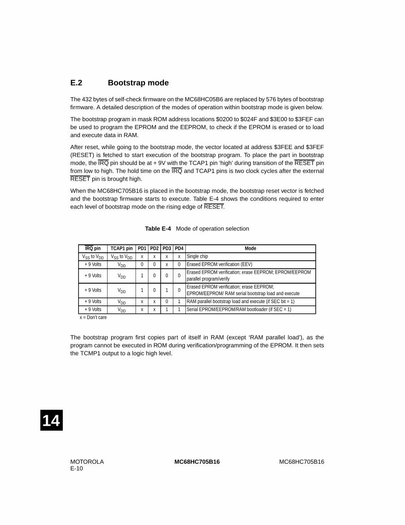
MOTOROLAE-10
MC68HC705B16MC68HC705B16
14
E.2 Bootstrap mode
The 432 bytes of self-check firmware on the MC68HC05B6 are replaced by 576 bytes of bootstrapfirmware. A detailed description of the modes of operation within bootstrap mode is given below.
The bootstrap program in mask ROM address locations $0200 to $024F and $3E00 to $3FEF canbe used to program the EPROM and the EEPROM, to check if the EPROM is erased or to loadand execute data in RAM.
After reset, while going to the bootstrap mode, the vector located at address $3FEE and $3FEF(RESET) is fetched to start execution of the bootstrap program. To place the part in bootstrapmode, the IRQ pin should be at + 9V with the TCAP1 pin ‘high’ during transition of the RESET pinfrom low to high. The hold time on the IRQ and TCAP1 pins is two clock cycles after the externalRESET pin is brought high.
When the MC68HC705B16 is placed in the bootstrap mode, the bootstrap reset vector is fetchedand the bootstrap firmware starts to execute. Table E-4 shows the conditions required to entereach level of bootstrap mode on the rising edge of RESET.
The bootstrap program first copies part of itself in RAM (except ‘RAM parallel load’), as theprogram cannot be executed in ROM during verification/programming of the EPROM. It then setsthe TCMP1 output to a logic high level.
Table E-4 Mode of operation selection
IRQ pin TCAP1 pin PD1 PD2 PD3 PD4 Mode
VSS to VDD VSS to VDD x x x x Single chip
+ 9 Volts VDD 0 0 x 0 Erased EPROM verification (EEV)
+ 9 Volts VDD 1 0 0 0Erased EPROM verification; erase EEPROM; EPROM/EEPROMparallel program/verify
+ 9 Volts VDD 1 0 1 0Erased EPROM verification; erase EEPROM;EPROM/EEPROM/ RAM serial bootstrap load and execute
+ 9 Volts VDD x x 0 1 RAM parallel bootstrap load and execute (if SEC bit = 1)
+ 9 Volts VDD x x 1 1 Serial EPROM/EEPROM/RAM bootloader (if SEC = 1)
x = Don’t care
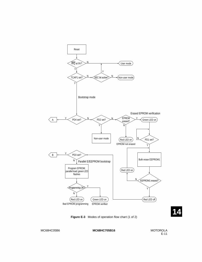
MC68HC05B6 MOTOROLAE-11
MC68HC705B16
14Figure E-3 Modes of operation flow chart (1 of 2)
PD3 set?
EEPROM1 erased?
TCAP1 set?
IRQ at 9V?
PD2 set?PD4 set?
Reset
Program EPROM;parallel load; green LED
flashes
User mode
Green LED on
Red LED onNon-user mode
Red LED on Green LED on
Non-user mode
A
N
YY
Y
Y N
Y N
N
N Y
N
Y
Bootstrap mode
EPROM not erased
EPROM verified
Parallel E/EEPROM bootstrap
Bad EPROM programming
N
PD1 set?
Bulk erase EEPROM1
Red LED on
Red LED off
N
Y
Y
N
B
N
Y
Erased EPROM verification
SEC bit active?
EPROMerased?
Programming OK?
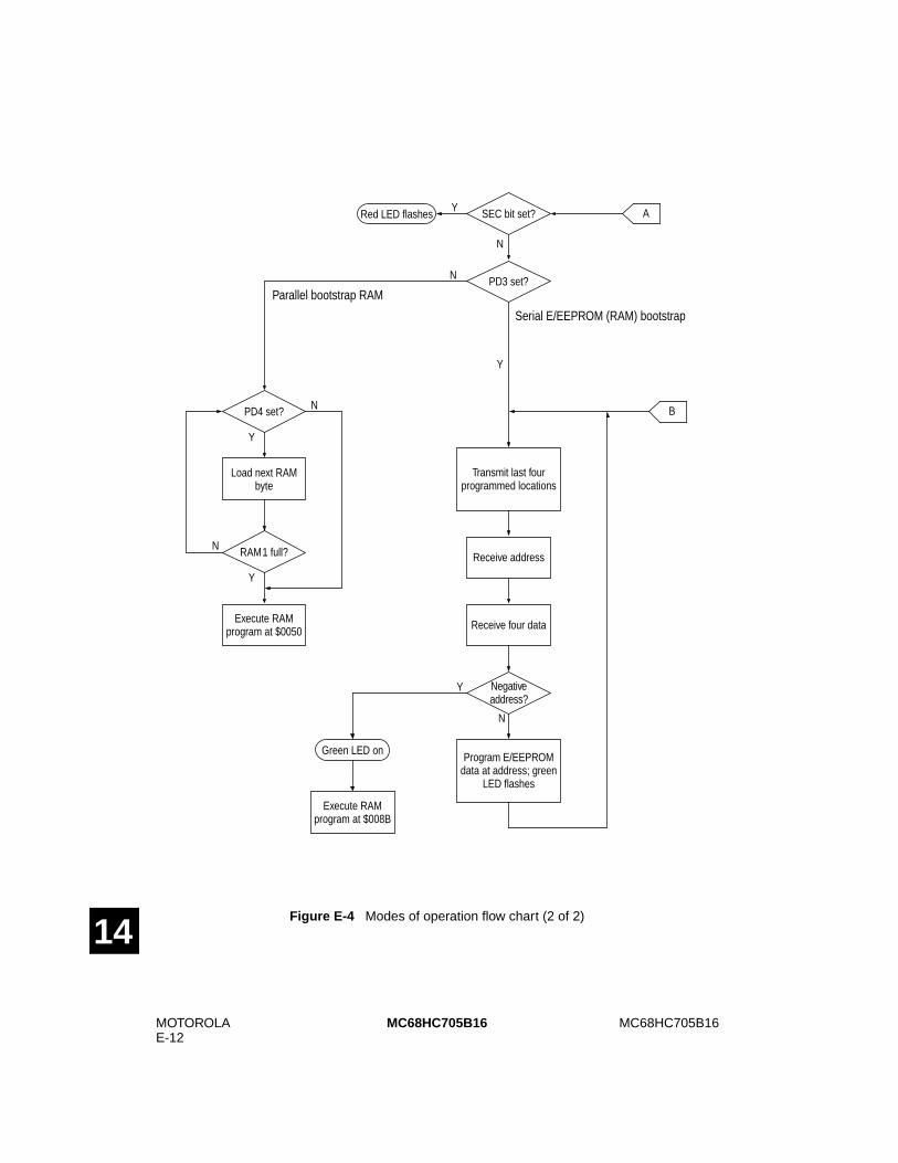
MOTOROLAE-12
MC68HC705B16MC68HC705B16
14Figure E-4 Modes of operation flow chart (2 of 2)
Negativeaddress?
PD4 set?
PD3 set?
Transmit last fourprogrammed locations
A
Receive address
Receive four data
Execute RAMprogram at $008B
Green LED on
Load next RAMbyte
RAM1 full?
Execute RAMprogram at $0050
Program E/EEPROMdata at address; green
LED flashes
N
Y
Y
Y
Y
N
N
Serial E/EEPROM (RAM) bootstrap
Parallel bootstrap RAM
SEC bit set?Red LED flashes
B
N
Y
N
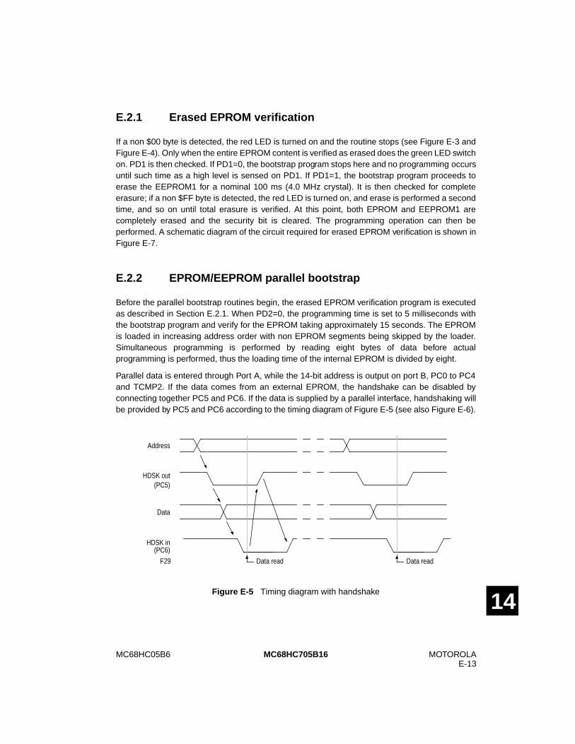
MC68HC05B6 MOTOROLAE-13
MC68HC705B16
14
E.2.1 Erased EPROM verification
If a non $00 byte is detected, the red LED is turned on and the routine stops (see Figure E-3 andFigure E-4). Only when the entire EPROM content is verified as erased does the green LED switchon. PD1 is then checked. If PD1=0, the bootstrap program stops here and no programming occursuntil such time as a high level is sensed on PD1. If PD1=1, the bootstrap program proceeds toerase the EEPROM1 for a nominal 100 ms (4.0 MHz crystal). It is then checked for completeerasure; if a non $FF byte is detected, the red LED is turned on, and erase is performed a secondtime, and so on until total erasure is verified. At this point, both EPROM and EEPROM1 arecompletely erased and the security bit is cleared. The programming operation can then beperformed. A schematic diagram of the circuit required for erased EPROM verification is shown inFigure E-7.
E.2.2 EPROM/EEPROM parallel bootstrap
Before the parallel bootstrap routines begin, the erased EPROM verification program is executedas described in Section E.2.1. When PD2=0, the programming time is set to 5 milliseconds withthe bootstrap program and verify for the EPROM taking approximately 15 seconds. The EPROMis loaded in increasing address order with non EPROM segments being skipped by the loader.Simultaneous programming is performed by reading eight bytes of data before actualprogramming is performed, thus the loading time of the internal EPROM is divided by eight.
Parallel data is entered through Port A, while the 14-bit address is output on port B, PC0 to PC4and TCMP2. If the data comes from an external EPROM, the handshake can be disabled byconnecting together PC5 and PC6. If the data is supplied by a parallel interface, handshaking willbe provided by PC5 and PC6 according to the timing diagram of Figure E-5 (see also Figure E-6).
Figure E-5 Timing diagram with handshake
Data read Data read
Address
HDSK out(PC5)
Data
HDSK in(PC6)
F29
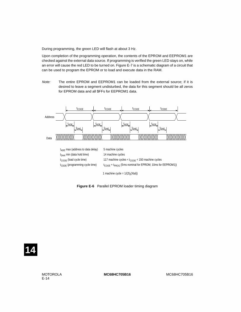
MOTOROLAE-14
MC68HC705B16MC68HC705B16
14
During programming, the green LED will flash at about 3 Hz.
Upon completion of the programming operation, the contents of the EPROM and EEPROM1 arechecked against the external data source. If programming is verified the green LED stays on, whilean error will cause the red LED to be turned on. Figure E-7 is a schematic diagram of a circuit thatcan be used to program the EPROM or to load and execute data in the RAM.
Note: The entire EPROM and EEPROM1 can be loaded from the external source; if it isdesired to leave a segment undisturbed, the data for this segment should be all zerosfor EPROM data and all $FFs for EEPROM1 data.
Figure E-6 Parallel EPROM loader timing diagram
tCOOE
tADEtDHE
Address
Data
tADEtDHE
tADEtDHE
tADEtDHE
tCOOE tCOOE tCDDE
tADE max (address to data delay) 5 machine cycles
tDHA min (data hold time) 14 machine cycles
tCOOE (load cycle time) 117 machine cycles < tCOOE < 150 machine cycles
tCDDE (programming cycle time) tCOOE + tPROG (5ms nominal for EPROM; 10ms for EEPROM1))
1 machine cycle = 1/(2f0(Xtal))
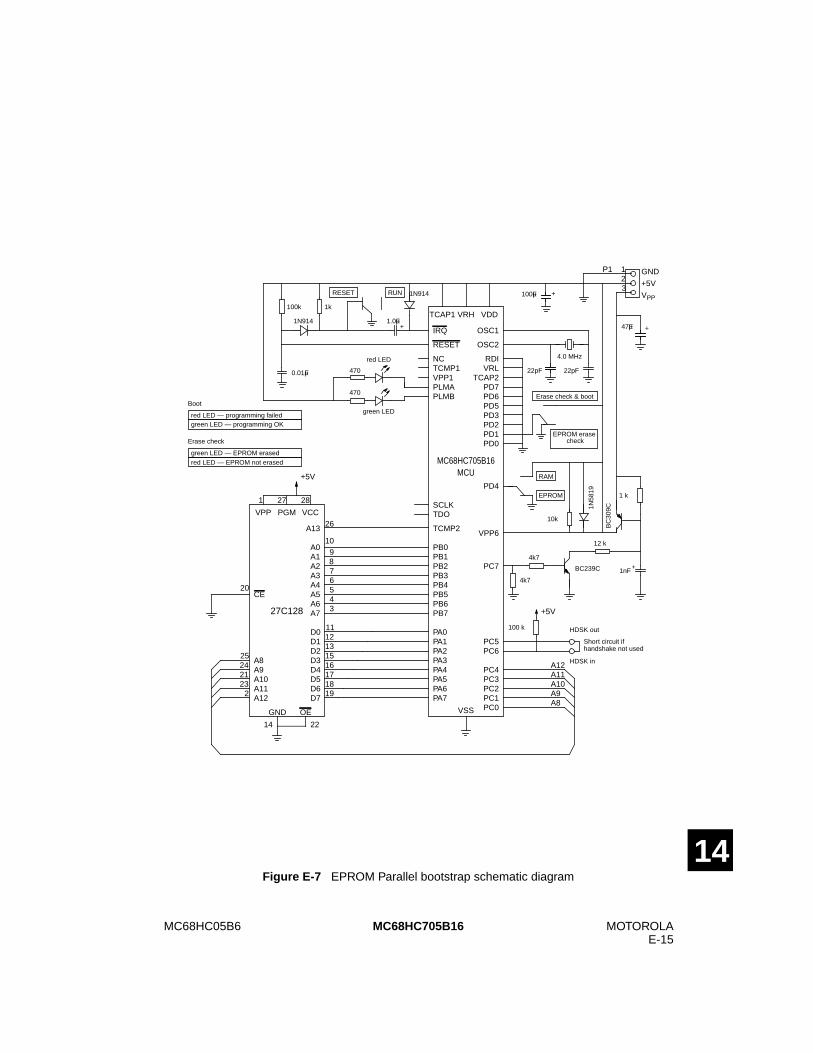
MC68HC05B6 MOTOROLAE-15
MC68HC705B16
14Figure E-7 EPROM Parallel bootstrap schematic diagram
VCC
281
VPP PGM
27
PB0PB1PB2PB3PB4PB5PB6PB7
PA0PA1PA2PA3PA4PA5PA6PA7
VDD
OSC1
OSC2
TCAP1
IRQ
RESET
VSS
A0A1A2A3A4A5A6A7
D0D1D2D3D4D5D6D7
GND OE
14 22
10987654
26
12131516171819
11
3
+5V
12
P1 GND
+5V100µF
22pF
4.0 MHz
1N914
1k½
1.0µF
22pF
100k½
1N914
RESET RUN
0.01µF
TDOSCLK
RDIVRL
TCAP2PD7PD6PD5PD3PD2PD1PD0
PD4
+5V
3VPP
VPP6
PC7
PC5
PC4PC3PC2PC1PC0
PC6
242123
2
A9A8
A10
A12
CE
A11
A12A11A10A9A8
HDSK out
HDSK in
Short circuit ifhandshake not used
100 k½
NCTCMP1
TCMP2
PLMAPLMB
470½
470½
red LED
green LED
4k7½
4k7½
12 k½
BC239C
BC
309C
10k ½
27C128
+
+
VRH
red LED — programming failedgreen LED — programming OK
25
1nF
1N58
19
1 k½
+
RAM
EPROM
green LED — EPROM erased
47µF +
Erase check & boot
EPROM erase check
VPP1
red LED — EPROM not erased
Boot
Erase check
A13
20
MC68HC705B16MCU
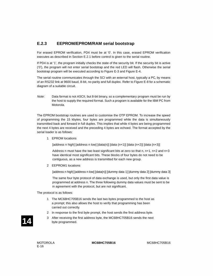
MOTOROLAE-16
MC68HC705B16MC68HC705B16
14
E.2.3 EEPROM/EPROM/RAM serial bootstrap
For erased EPROM verification, PD4 must be at ‘0’. In this case, erased EPROM verificationexecutes as described in Section E.2.1 before control is given to the serial routine.
If PD4 is at ‘1’, the program initially checks the state of the security bit. If the security bit is active(‘0’), the program will not enter serial bootstrap and the red LED will flash. Otherwise the serialbootstrap program will be executed according to Figure E-3 and Figure E-4.
The serial routine communicates through the SCI with an external host, typically a PC, by meansof an RS232 link at 9600 baud, 8-bit, no parity and full duplex. Refer to Figure E-8 for a schematicdiagram of a suitable circuit.
Note: Data format is not ASCII, but 8-bit binary, so a complementary program must be run bythe host to supply the required format. Such a program is available for the IBM PC fromMotorola.
The EPROM bootstrap routines are used to customise the OTP EPROM. To increase the speedof programming the 15 kbytes, four bytes are programmed while the data is simultaneouslytransmitted back and forward in full duplex. This implies that while 4 bytes are being programmedthe next 4 bytes are received and the preceding 4 bytes are echoed. The format accepted by theserial loader is as follows:
1 EPROM locations
[address n high] [address n low] [data(n)] [data (n+1)] [data (n+2)] [data (n+3)]
Address n must have the two least significant bits at zero so that n, n+1, n+2 and n+3have identical most significant bits. These blocks of four bytes do not need to becontiguous, as a new address is transmitted for each new group.
2 EEPROM1 locations
[address n high] [address n low] [data(n)] [dummy data 1] [dummy data 2] [dummy data 3]
The same four byte protocol of data exchange is used, but only the first data value isprogrammed at address n. The three following dummy data values must be sent to bein agreement with the protocol, but are not significant.
The protocol is as follows:
1 The MC68HC705B16 sends the last two bytes programmed to the host asa prompt; this also allows the host to verify that programming has beencarried out correctly.
2 In response to the first byte prompt, the host sends the first address byte.
3 After receiving the first address byte, the MC68HC705B16 sends the nextbyte programmed.
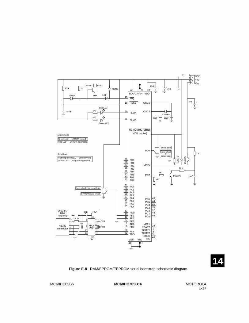
MC68HC05B6 MOTOROLAE-17
MC68HC705B16
14Figure E-8 RAM/EPROM/EEPROM serial bootstrap schematic diagram
Green LED — programming endedFlashing green LED — programming
40
VPP6
PC7
PB0PB1PB2PB3PB4PB5PB6PB7
PA0PA1PA2PA3PA4PA5PA6PA7
VDD
OSC1
OSC2
TCAP1
IRQ
RESET
VSS
12
P1 GND
+5V
1N9141k½
1.0µF
100k½
1N914
RESET RUN
0.01µF
3VPP
PC5PC4PC3PC2PC1PC0
PC6
PLMA
PLMB
470½
470½
Red LED
Green LED
+
+
VRH
22µF
22µF
22µF
2 x 3K½ 12
34
8
675
111213
14
15
16
5321
22µF
RS232connector
MAX232
+5V9600 BD
8-bitno parity
19
18
20
21
5052
3938373635343332
3130292827262524
14131254
43444546474849
232151
22 8 10
41 7
VRL
TCAP2TCMP1TCMP2
SCLKNC
10nF47µF
PD0
PD4
PD1PD2PD5PD6PD7
+
+
+
+
22pF
4.0 MHz
22pF
4k7½
4k7½
12 k½
BC239C
BC
309C
10k ½
1nF1N
5819
1 k½
+
Serial boot
Erase check
47µF +
PD3
RDITDO
Erase check
Red LED — EPROM not erasedGreen LED — EPROM erased
Serial boot &serial boot
Erase check and serial boot
EPROM erase check
VPP13
U2 MC68HC705B16MCU (socket)
MOTOROLAE-18
MC68HC705B16MC68HC705B16
14
4 The exchange of data continues until the MC68HC705B16 has sent the fourdata bytes and the host has sent the 2 address data bytes and 4 data bytes.
5 If the data is different from $00 for EPROM or $FF for EEPROM, it isprogrammed at the address provided, while the next address and bytes arereceived and the previous data is echoed.
6 Loop to 1.
After reset, the MC68HC705B16 serial bootstrap routine will first echo two blocks of four bytes at$00, as no data is programmed yet.
If the data received is $00 for EPROM locations or $FF for EEPROM locations, no programmingin the EPROM and EEPROM1 takes place, and the contents of the accessed location are returnedas a prompt. The entire EPROM/EEPROM memory can be read in this fashion (serial dump).
Warning: When using this function with a programmed device, the device must be placed intoRAM/EPROM/EEPROM serial bootstrap mode without EPROM erase check (PD4 = 1).
Serial RAM loading and execute can be accomplished in this mode. A RAM byte will be written ifthe address sent by the host in the serial protocol points to the RAM.
RAM bytes $008B–$00E3 and $0250–$02ED are available for user test programs. A 10-byte stackresides at the top of RAMI, allowing, for example, one interrupt and two sub-routine levels. TheRAM addresses between $0050 and $008A are used by the loader and are therefore not availableto the user during serial loading/executing.
If the SEC bit is at ‘1’, program execution is triggered by sending a negative (bit 7 set) highaddress; execution starts at address XADR ($008B).
In the RAM bootloader mode, all interrupt vectors are mapped to pseudo-vectors in RAM (seeTable E-5). This allows programmers to use their own service-routine addresses. Eachpseudo-vector is allowed three bytes of space rather than the two bytes for normal vectors,because an explicit jump (JMP) opcode is needed to cause the desired jump to the user’s serviceroutine address.
Table E-5 Bootstrap vector targets in RAM
Vector targets in RAM
SCI interrupt $02EE
Timer overflow $02F1
Timer output compare $02F4
Timer input capture $02F7
IRQ $02FA
SWI $02FD
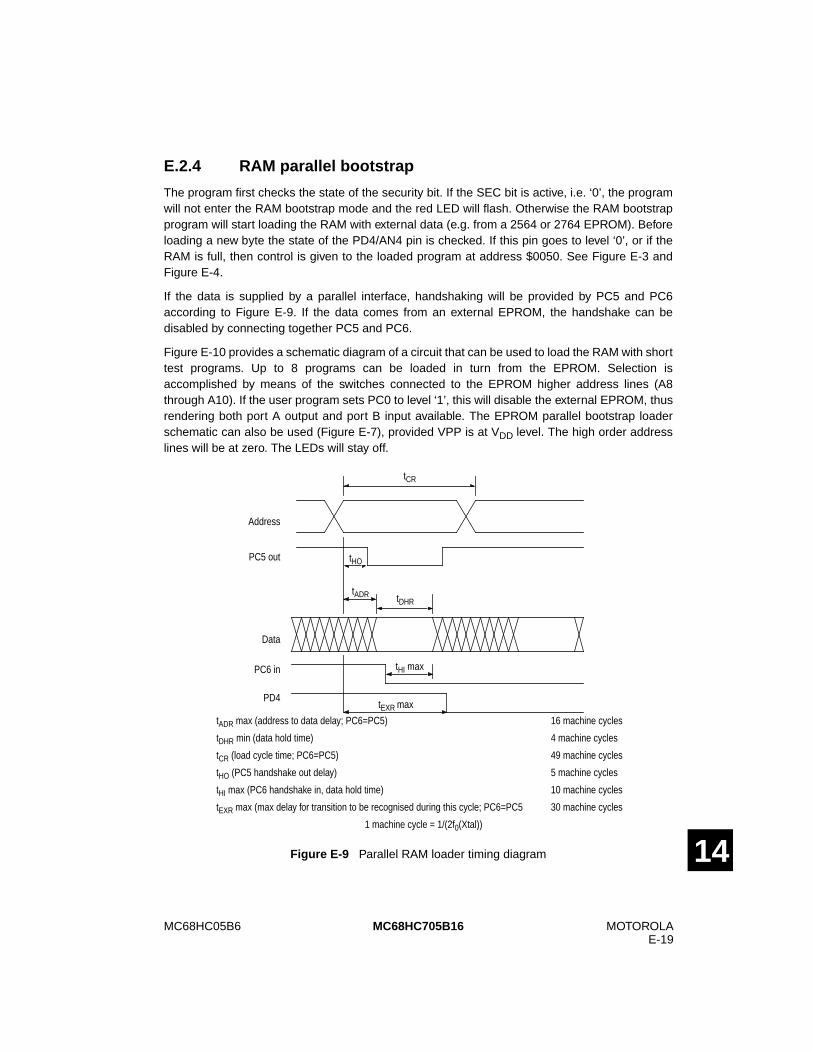
MC68HC05B6 MOTOROLAE-19
MC68HC705B16
14
E.2.4 RAM parallel bootstrap
The program first checks the state of the security bit. If the SEC bit is active, i.e. ‘0’, the programwill not enter the RAM bootstrap mode and the red LED will flash. Otherwise the RAM bootstrapprogram will start loading the RAM with external data (e.g. from a 2564 or 2764 EPROM). Beforeloading a new byte the state of the PD4/AN4 pin is checked. If this pin goes to level ‘0’, or if theRAM is full, then control is given to the loaded program at address $0050. See Figure E-3 andFigure E-4.
If the data is supplied by a parallel interface, handshaking will be provided by PC5 and PC6according to Figure E-9. If the data comes from an external EPROM, the handshake can bedisabled by connecting together PC5 and PC6.
Figure E-10 provides a schematic diagram of a circuit that can be used to load the RAM with shorttest programs. Up to 8 programs can be loaded in turn from the EPROM. Selection isaccomplished by means of the switches connected to the EPROM higher address lines (A8through A10). If the user program sets PC0 to level ‘1’, this will disable the external EPROM, thusrendering both port A output and port B input available. The EPROM parallel bootstrap loaderschematic can also be used (Figure E-7), provided VPP is at VDD level. The high order addresslines will be at zero. The LEDs will stay off.
Figure E-9 Parallel RAM loader timing diagram
tADR tDHR
Address
Data
tCR
PD4tEXR max
tHO
tHI max
PC5 out
PC6 in
tADR max (address to data delay; PC6=PC5) 16 machine cycles
tDHR min (data hold time) 4 machine cycles
tCR (load cycle time; PC6=PC5) 49 machine cycles
tHO (PC5 handshake out delay) 5 machine cycles
tHI max (PC6 handshake in, data hold time) 10 machine cycles
tEXR max (max delay for transition to be recognised during this cycle; PC6=PC5 30 machine cycles
1 machine cycle = 1/(2f0(Xtal))
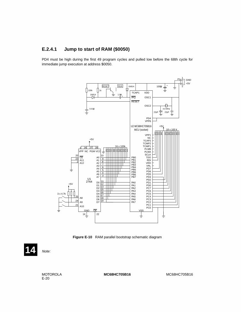
MOTOROLAE-20
MC68HC705B16MC68HC705B16
14
E.2.4.1 Jump to start of RAM ($0050)
PD4 must be high during the first 49 program cycles and pulled low before the 68th cycle forimmediate jump execution at address $0050.
Note:
Figure E-10 RAM parallel bootstrap schematic diagram
PB0PB1PB2PB3PB4PB5PB6PB6PB7
PA0PA1PA2PA3PA4PA5PA6PA7
VDD
TCAP2TCMP2TCMP1
PLMBPLMASCLKTDORDI
VRHVRLPD7PD6PD5PD3PD2PD1PD0PC7PC6PC5PC4PC3PC2PC1PC0
NC
OSC1
OSC2
TCAP1
IRQ
RESET
PD4VPP6
VSS
A0A1A2A3A4A5A6A7
D0D1D2D3D4D5D6D7
GND OE
A8
A9
A10
A11A12
CE
VCCPGMVPP
20
2
25
24
23
14 22
10987654
1 26 27 28
21
12131516171819
11
3
+5V
3 x 4.7k½
+5V
16 x 100k½
1
2
P1 GND
+5V100µF
22pF
4.0 MHz
1N914
1k½
1.0µF
22pF
100k½
1N914
RESET RUN
0.01µF
U12764
+5V18 x 100 k½
+
+
NC
VPP1
U2 MC68HC705B16MCU (socket)
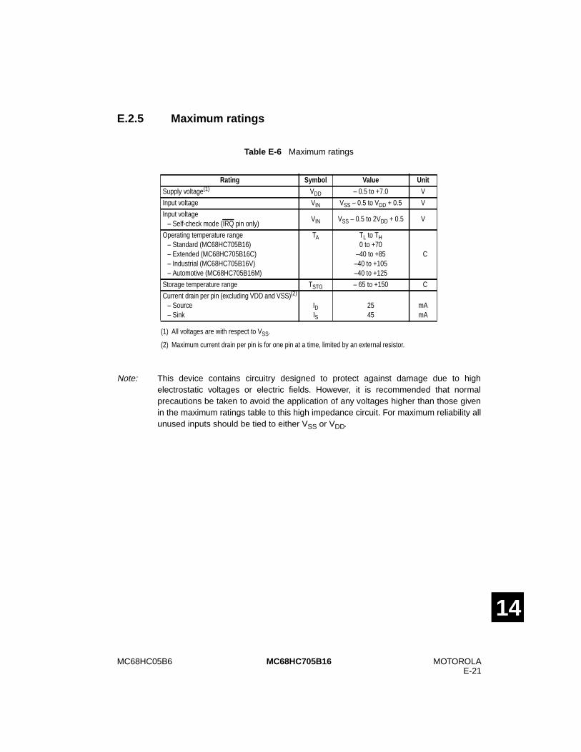
MC68HC05B6 MOTOROLAE-21
MC68HC705B16
14
E.2.5 Maximum ratings
Note: This device contains circuitry designed to protect against damage due to highelectrostatic voltages or electric fields. However, it is recommended that normalprecautions be taken to avoid the application of any voltages higher than those givenin the maximum ratings table to this high impedance circuit. For maximum reliability allunused inputs should be tied to either VSS or VDD.
(1) All voltages are with respect to VSS.
(2) Maximum current drain per pin is for one pin at a time, limited by an external resistor.
Table E-6 Maximum ratings
Rating Symbol Value Unit
Supply voltage(1) VDD – 0.5 to +7.0 V
Input voltage VIN VSS – 0.5 to VDD + 0.5 V
Input voltage– Self-check mode (IRQ pin only)
VIN VSS – 0.5 to 2VDD + 0.5 V
Operating temperature range– Standard (MC68HC705B16)– Extended (MC68HC705B16C)– Industrial (MC68HC705B16V)– Automotive (MC68HC705B16M)
TA TL to TH0 to +70
–40 to +85–40 to +105–40 to +125
¡C
Storage temperature range TSTG – 65 to +150 ¡C
Current drain per pin (excluding VDD and VSS)(2)
– Source– Sink
IDIS
2545
mAmA
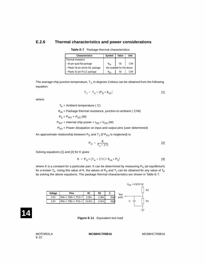
MOTOROLAE-22
MC68HC705B16MC68HC705B16
14
E.2.6 Thermal characteristics and power considerations
The average chip junction temperature, TJ, in degrees Celsius can be obtained from the following
equation:
[1]
where:
TA = Ambient temperature (¡C)
θJA = Package thermal resistance, junction-to-ambient (¡C/W)
PD = PINT + PI/O (W)
PINT = Internal chip power = IDD • VDD (W)
PI/O = Power dissipation on input and output pins (user determined)
An approximate relationship between PD and TJ (if PI/O is neglected) is:
[2]
Solving equations [1] and [2] for K gives:
[3]
where K is a constant for a particular part. K can be determined by measuring PD (at equilibrium)for a known TA. Using this value of K, the values of PD and TJ can be obtained for any value of TAby solving the above equations. The package thermal characteristics are shown in Table E-7.
Table E-7 Package thermal characteristics
Characteristics Symbol Value Unit
Thermal resistance
– 64-pin quad flat package θJA 50 ¡C/W
– Plastic 56 pin shrink DIL package Not available for this device
– Plastic 52 pin PLCC package θJA 50 ¡C/W
Figure E-11 Equivalent test load
TJ TA PD θJA•( )+=
PDK
TJ 273+---------------------=
K PD TA 273+( )• θJA PD2•+=
VDD = 4.5/3.0 V
R2
R1C
Testpoint
Voltage Pins R1 R2 C
4.5V PA0–7, PB0–7, PC0–7 3.26k½ 2.38k½ 50pF
3.0V PA0–7, PB0–7, PC0–7 10.91k½ 6.32k½ 50pF

MC68HC05B6 MOTOROLAE-23
MC68HC705B16
14
E.2.7 DC electrical characteristicsTable E-8 DC electrical characteristics for 5V operation
(VDD = 5 Vdc ± 10%, VSS = 0 Vdc, TA = TL to TH)Characteristic (1) Symbol Min Typ (2) Max Unit
Output voltageILOAD = – 10 µAILOAD = +10 µA
VOHVOL
VDD – 0.1—
——
—0.1
V
Output high voltage (ILOAD = 0.8mA)PA0–7, PB0–7, PC0–7, TCMP1, TCMP2
Output high voltage (ILOAD = 1.6mA)TDO, SCLK, PLMA, PLMB
VOH
VOH
VDD – 0.8
VDD – 0.8
VDD – 0.4
VDD – 0.4
—
—
V
Output low voltage (ILOAD = 1.6mA)PA0–7, PB0–7, PC0–7, TCMP1, TCMP2,
TDO, SCLK, PLMA, PLMBOutput low voltage (ILOAD = 1.6mA)
RESET
VOL
VOL
— 0.1
0.4
0.4
1
V
Input high voltagePA0–7, PB0–7, PC0–7, PD0–7, OSC1,IRQ, RESET, TCAP1, TCAP2, RDI
VIH 0.7VDD — VDD V
Input low voltagePA0–7, PB0–7, PC0–7, PD0–7, OSC1,IRQ, RESET, TCAP1, TCAP2, RDI
VIL VSS — 0.2VDD V
Supply current(3)
RUN (SM = 0) (See Figure 11-2)RUN (SM = 1) (See Figure 11-3)WAIT (SM = 0) (See Figure 11-4)WAIT (SM = 1) (See Figure 11-5)STOP
0 to 70 (standard)– 40 to 85 (extended)– 40 to 105 (industrial)– 40 to 125 (automotive)
IDDIDDIDDIDD
IDDIDDIDDIDD
————
————
5.01.01.50.9
2———
61.521
10206060
mAmAmAmA
µAµAµAµA
EPROMAbsolute maximum voltageProgramming voltageProgramming currentRead voltage
VPP6 maxVPP6IPP6
VPP6R
VDD15—
VDD
—15.550
VDD
181664
VDD±10%
VV
mAV
High-Z leakage currentPA0–7, PB0–7, PC0–7, TDO, RESET, SCLK IIL — ±0.2 ±1 µA
Input currentPort B and port C pull-down (VIN=VIH) IRPD 80 µA
Input current (0 to 70)IRQ, OSC1, TCAP1, TCAP2, RDI,PD0/AN0-PD7/AN7 (channel not selected)
IIN — ±0.2 ±1 µA
Input current (– 40 to 125)IRQ, OSC1, TCAP1, TCAP2, RDI,PD0/AN0-PD7/AN7 (channel not selected)
IIN — — ±5 µA
CapacitancePorts (as input or output), RESET, TDO, SCLKIRQ, TCAP1, TCAP2, OSC1, RDIPD0/AN0–PD7/AN7 (A/D off)PD0/AN0–PD7/AN7 (A/D on)
COUTCINCINCIN
————
——1222
128——
pFpFpFpF
MOTOROLAE-24
MC68HC705B16MC68HC705B16
14
(1) All IDD measurements taken with suitable decoupling capacitors across the power supply to suppress thetransient switching currents inherent in CMOS designs (see Section 2).
(2) Typical values are at mid point of voltage range and at 25¡C only.
(3) RUN and WAIT IDD: measured using an external square-wave clock source (fOSC = 4.2MHz); all inputs 0.2 Vfrom rail; no DC loads; maximum load on outputs 50pF (20pF on OSC2).STOP /WAIT IDD: all ports configured as inputs; VIL = 0.2 V and VIH = VDD – 0.2 V: STOP IDD measured withOSC1 = VDD.WAIT IDD is affected linearly by the OSC2 capacitance.
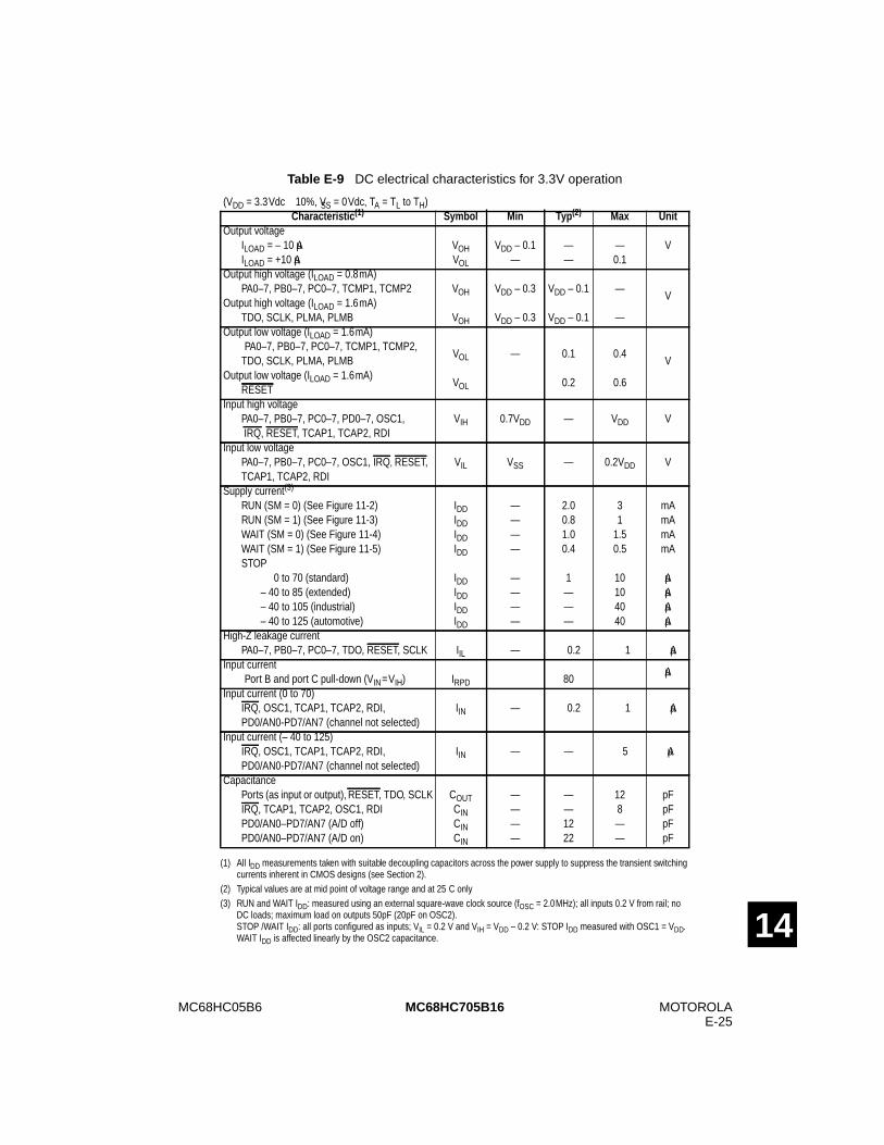
MC68HC05B6 MOTOROLAE-25
MC68HC705B16
14
(1) All IDD measurements taken with suitable decoupling capacitors across the power supply to suppress the transient switchingcurrents inherent in CMOS designs (see Section 2).
(2) Typical values are at mid point of voltage range and at 25¡C only.(3) RUN and WAIT IDD: measured using an external square-wave clock source (fOSC = 2.0MHz); all inputs 0.2 V from rail; no
DC loads; maximum load on outputs 50pF (20pF on OSC2).STOP /WAIT IDD: all ports configured as inputs; VIL = 0.2 V and VIH = VDD – 0.2 V: STOP IDD measured with OSC1 = VDD.WAIT IDD is affected linearly by the OSC2 capacitance.
Table E-9 DC electrical characteristics for 3.3V operation
(VDD = 3.3Vdc ± 10%, VSS = 0Vdc, TA = TL to TH)Characteristic (1) Symbol Min Typ (2) Max Unit
Output voltageILOAD = – 10 µAILOAD = +10 µA
VOHVOL
VDD – 0.1—
——
—0.1
V
Output high voltage (ILOAD = 0.8mA)PA0–7, PB0–7, PC0–7, TCMP1, TCMP2
Output high voltage (ILOAD = 1.6mA)TDO, SCLK, PLMA, PLMB
VOH
VOH
VDD – 0.3
VDD – 0.3
VDD – 0.1
VDD – 0.1
—
—
V
Output low voltage (ILOAD = 1.6mA)PA0–7, PB0–7, PC0–7, TCMP1, TCMP2,
TDO, SCLK, PLMA, PLMBOutput low voltage (ILOAD = 1.6mA)
RESET
VOL
VOL
— 0.1
0.2
0.4
0.6
V
Input high voltagePA0–7, PB0–7, PC0–7, PD0–7, OSC1,IRQ, RESET, TCAP1, TCAP2, RDI
VIH 0.7VDD — VDD V
Input low voltagePA0–7, PB0–7, PC0–7, OSC1, IRQ, RESET,TCAP1, TCAP2, RDI
VIL VSS — 0.2VDD V
Supply current(3)
RUN (SM = 0) (See Figure 11-2)RUN (SM = 1) (See Figure 11-3)WAIT (SM = 0) (See Figure 11-4)WAIT (SM = 1) (See Figure 11-5)STOP
0 to 70 (standard)– 40 to 85 (extended)– 40 to 105 (industrial)– 40 to 125 (automotive)
IDDIDDIDDIDD
IDDIDDIDDIDD
————
————
2.00.81.00.4
1———
31
1.50.5
10104040
mAmAmAmA
µAµAµAµA
High-Z leakage currentPA0–7, PB0–7, PC0–7, TDO, RESET, SCLK IIL — ±0.2 ±1 µA
Input currentPort B and port C pull-down (VIN=VIH) IRPD 80
µA
Input current (0 to 70)IRQ, OSC1, TCAP1, TCAP2, RDI,PD0/AN0-PD7/AN7 (channel not selected)
IIN — ±0.2 ±1 µA
Input current (– 40 to 125)IRQ, OSC1, TCAP1, TCAP2, RDI,PD0/AN0-PD7/AN7 (channel not selected)
IIN — — ±5 µA
CapacitancePorts (as input or output), RESET, TDO, SCLKIRQ, TCAP1, TCAP2, OSC1, RDIPD0/AN0–PD7/AN7 (A/D off)PD0/AN0–PD7/AN7 (A/D on)
COUTCINCINCIN
————
——1222
128——
pFpFpFpF
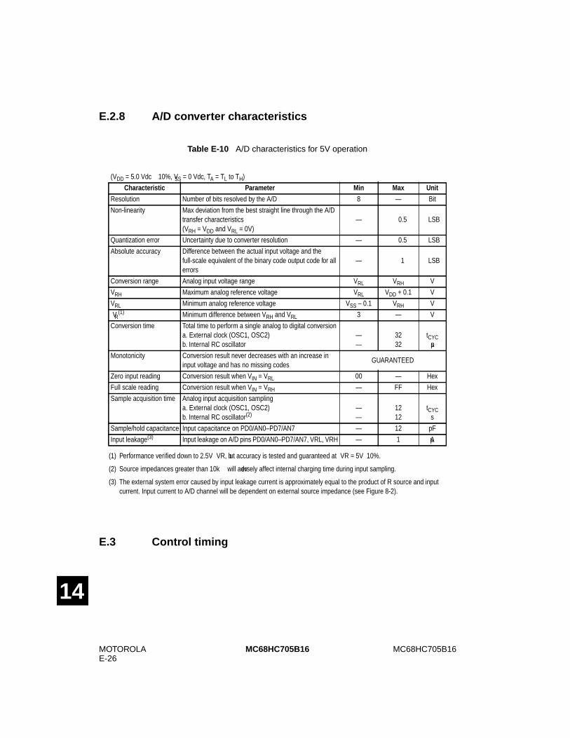
MOTOROLAE-26
MC68HC705B16MC68HC705B16
14
E.2.8 A/D converter characteristics
E.3 Control timing
(1) Performance verified down to 2.5V ÆVR, but accuracy is tested and guaranteed at ÆVR = 5V±10%.
(2) Source impedances greater than 10k½ will adversely affect internal charging time during input sampling.
(3) The external system error caused by input leakage current is approximately equal to the product of R source and inputcurrent. Input current to A/D channel will be dependent on external source impedance (see Figure 8-2).
Table E-10 A/D characteristics for 5V operation
(VDD = 5.0 Vdc ± 10%, VSS = 0 Vdc, TA = TL to TH)
Characteristic Parameter Min Max Unit
Resolution Number of bits resolved by the A/D 8 — Bit
Non-linearity Max deviation from the best straight line through the A/Dtransfer characteristics(VRH = VDD and VRL = 0V)
— ± 0.5 LSB
Quantization error Uncertainty due to converter resolution — ± 0.5 LSB
Absolute accuracy Difference between the actual input voltage and thefull-scale equivalent of the binary code output code for allerrors
— ± 1 LSB
Conversion range Analog input voltage range VRL VRH V
VRH Maximum analog reference voltage VRL VDD + 0.1 V
VRL Minimum analog reference voltage VSS – 0.1 VRH V
ÆVR(1) Minimum difference between VRH and VRL 3 — V
Conversion time Total time to perform a single analog to digital conversiona. External clock (OSC1, OSC2)b. Internal RC oscillator
——
3232
tCYCµs
Monotonicity Conversion result never decreases with an increase ininput voltage and has no missing codes
GUARANTEED
Zero input reading Conversion result when VIN = VRL 00 — Hex
Full scale reading Conversion result when VIN = VRH — FF Hex
Sample acquisition time Analog input acquisition samplinga. External clock (OSC1, OSC2)b. Internal RC oscillator(2)
——
1212
tCYCs
Sample/hold capacitance Input capacitance on PD0/AN0–PD7/AN7 — 12 pF
Input leakage(3) Input leakage on A/D pins PD0/AN0–PD7/AN7, VRL, VRH — 1 µA

MC68HC05B6 MOTOROLAE-27
MC68HC705B16
14
(1) Source impedances greater than 10k½ will adversely affect internal charging time during input sampling.
(2) The external system error caused by input leakage current is approximately equal to the product of R source and inputcurrent. Input current to A/D channel will be dependent on external source impedance (see Figure 8-2).
Table E-11 A/D characteristics for 3.3V operation
(VDD = 3.3 Vdc ± 10%, VSS = 0 Vdc, TA = TL to TH)
Characteristic Parameter Min Max Unit
Resolution Number of bits resolved by the A/D 8 — Bit
Non-linearity Max deviation from the best straight line through the A/Dtransfer characteristics(VRH = VDD and VRL = 0V)
— ± 1 LSB
Quantization error Uncertainty due to converter resolution — ± 1 LSB
Absolute accuracy Difference between the actual input voltage and thefull-scale equivalent of the binary code output code for allerrors
— ± 2 LSB
Conversion range Analog input voltage range VRL VRH V
VRH Maximum analog reference voltage VRL VDD + 0.1 V
VRL Minimum analog reference voltage VSS – 0.1 VRH V
ÆVR Minimum difference between VRH and VRL 3 — V
Conversion time Total time to perform a single analog to digital conversionInternal RC oscillator — 32 µs
Monotonicity Conversion result never decreases with an increase ininput voltage and has no missing codes
GUARANTEED
Zero input reading Conversion result when VIN = VRL 00 — Hex
Full scale reading Conversion result when VIN = VRH — FF Hex
Sample acquisition time Analog input acquisition samplingInternal RC oscillator(1) — 12 s
Sample/hold capacitance Input capacitance on PD0/AN0–PD7/AN7 — 12 pF
Input leakage(2) Input leakage on A/D pins PD0/AN0–PD7/AN7, VRL, VRH — 1 µA
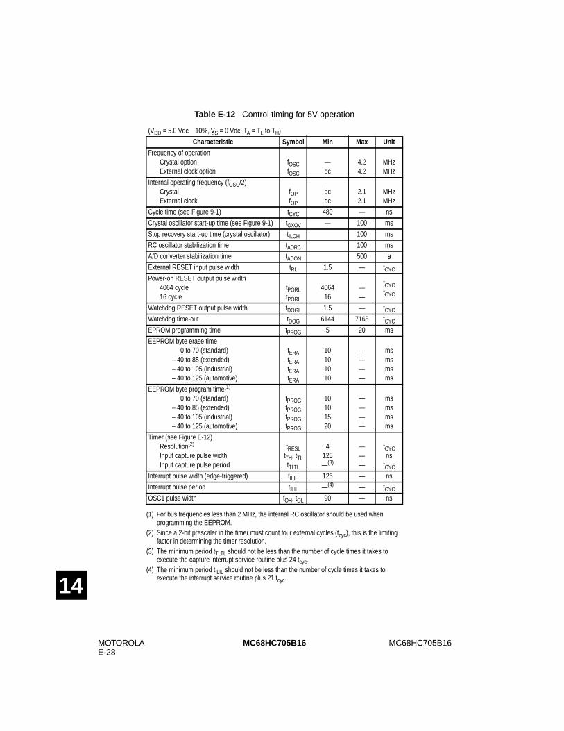
MOTOROLAE-28
MC68HC705B16MC68HC705B16
14
(1) For bus frequencies less than 2 MHz, the internal RC oscillator should be used whenprogramming the EEPROM.
(2) Since a 2-bit prescaler in the timer must count four external cycles (tcyc), this is the limitingfactor in determining the timer resolution.
(3) The minimum period tTLTL should not be less than the number of cycle times it takes toexecute the capture interrupt service routine plus 24 tcyc.
(4) The minimum period tILIL should not be less than the number of cycle times it takes toexecute the interrupt service routine plus 21 tcyc.
Table E-12 Control timing for 5V operation
(VDD = 5.0 Vdc ± 10%, VSS = 0 Vdc, TA = TL to TH)
Characteristic Symbol Min Max Unit
Frequency of operationCrystal optionExternal clock option
fOSCfOSC
—dc
4.24.2
MHzMHz
Internal operating frequency (fOSC/2)CrystalExternal clock
fOPfOP
dcdc
2.12.1
MHzMHz
Cycle time (see Figure 9-1) tCYC 480 — ns
Crystal oscillator start-up time (see Figure 9-1) tOXOV — 100 ms
Stop recovery start-up time (crystal oscillator) tILCH 100 ms
RC oscillator stabilization time tADRC 100 ms
A/D converter stabilization time tADON 500 µs
External RESET input pulse width tRL 1.5 — tCYC
Power-on RESET output pulse width4064 cycle16 cycle
tPORLtPORL
406416
——
tCYCtCYC
Watchdog RESET output pulse width tDOGL 1.5 — tCYC
Watchdog time-out tDOG 6144 7168 tCYC
EPROM programming time tPROG 5 20 ms
EEPROM byte erase time0 to 70 (standard)
– 40 to 85 (extended)– 40 to 105 (industrial)– 40 to 125 (automotive)
tERAtERAtERAtERA
10101010
————
msmsmsms
EEPROM byte program time(1)
0 to 70 (standard)– 40 to 85 (extended)– 40 to 105 (industrial)– 40 to 125 (automotive)
tPROGtPROGtPROGtPROG
10101520
————
msmsmsms
Timer (see Figure E-12)Resolution(2)
Input capture pulse widthInput capture pulse period
tRESLtTH, tTLtTLTL
4125—(3)
———
tCYCns
tCYC
Interrupt pulse width (edge-triggered) tILIH 125 — ns
Interrupt pulse period tILIL —(4) — tCYC
OSC1 pulse width tOH, tOL 90 — ns

MC68HC05B6 MOTOROLAE-29
MC68HC705B16
14
(1) For bus frequencies less than 2 MHz, the internal RC oscillator should be used whenprogramming the EEPROM.
(2) Since a 2-bit prescaler in the timer must count four external cycles (tcyc), this is the limitingfactor in determining the timer resolution.
(3) The minimum period tTLTL should not be less than the number of cycle times it takes toexecute the capture interrupt service routine plus 24 tcyc.
(4) The minimum period tILIL should not be less than the number of cycle times it takes toexecute the interrupt service routine plus 21 tcyc.
Table E-13 Control timing for 3.3V operation
(VDD = 3.3Vdc ± 10%, VSS = 0 Vdc, TA = TL to TH)
Characteristic Symbol Min Max Unit
Frequency of operationCrystal optionExternal clock option
fOSCfOSC
—dc
2.02.0
MHzMHz
Internal operating frequency (fOSC/2)CrystalExternal clock
fOPfOP
—dc
1.01.0
MHzMHz
Cycle time (see Figure 9-1) tCYC 1000 — ns
Crystal oscillator start-up time (see Figure 9-1) tOXOV — 100 ms
Stop recovery start-up time (crystal oscillator) tILCH 100 ms
RC oscillator stabilization time tADRC 100 ms
A/D converter stabilization time tADON 500 µs
External RESET input pulse width tRL 1.5 — tCYC
Power-on RESET output pulse width4064 cycle16 cycle
tPORLtPORL
406416
——
tCYCtCYC
Watchdog RESET output pulse width tDOGL 1.5 — tCYC
Watchdog time-out tDOG 6144 7168 tCYC
EPROM programming time tPROG 5 20 ms
EEPROM byte erase time0 to 70 (standard)
– 40 to 85 (extended)– 40 to 105 (industrial)– 40 to 125 (automotive)
tERAtERAtERAtERA
30303030
————
msmsmsms
EEPROM byte program time(1)
0 to 70 (standard)– 40 to 85 (extended)– 40 to 85 (industrial)– 40 to 125 (automotive)
tPROGtPROGtPROGtPROG
30303030
————
msmsmsms
Timer (see Figure E-12)Resolution(2)
Input capture pulse widthInput capture pulse period
tRESLtTH, tTLtTLTL
4250—(3)
———
tCYCns
tCYC
Interrupt pulse width (edge-triggered) tILIH 250 — ns
Interrupt pulse period tILIL —(4) — tCYC
OSC1 pulse width tOH, tOL 200 — ns
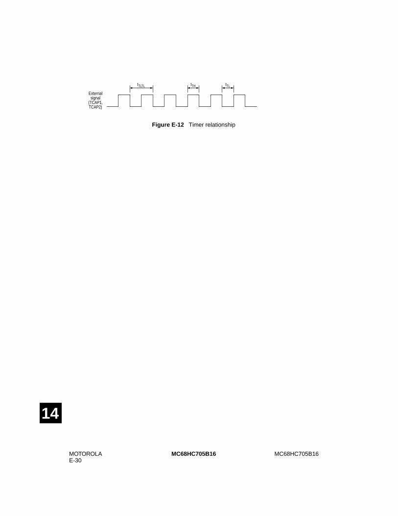
MOTOROLAE-30
MC68HC705B16MC68HC705B16
14
Figure E-12 Timer relationship
Externalsignal
(TCAP1,TCAP2)
tTLTL tTH tTL
MC68HC05B6 MOTOROLAF-1
MC68HC05B32
14
FMC68HC05B32
The MC68HC05B32 is a device similar to the MC68HC05B6, but with increased RAM and ROMsizes. The entire MC68HC05B6 data sheet applies to the MC68HC05B32, with the exceptionsoutlined in this appendix.
Features
• 31248 bytes User ROM
• No page zero ROM
• 528 bytes of RAM
• 638 bytes of self-check ROM
• 52-pin PLCC, 56-pin SDIP and 64-pin QFP packages
Note: Preliminary electrical specifications for the MC68HC05B32 should be taken as beingidentical to those for the MC68HC705B32. When silicon is fully available, the part willbe re-characterised and new data made available.
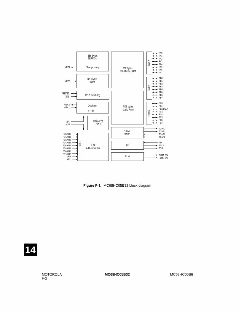
MOTOROLAF-2
MC68HC05B6MC68HC05B32
14
Figure F-1 MC68HC05B32 block diagram
Port
A
PA0PA1PA2PA3PA4PA5PA6PA7
Port
B
PB0PB1PB2PB3PB4PB5PB6PB7
Port
C
PC0PC1PC2/ECLKPC3PC4PC5PC6PC7
16-bittimer
Port
D
PD0/AN0PD1/AN1PD2/AN2PD3/AN3PD4/AN4PD5/AN5PD6/AN6PD7/AN7
Oscillator
COP watchdogRESET
IRQ
VDDVSS
OSC1OSC2
M68HC05CPU
SCIA/D converter
PLM
TCAP1TCAP2
TCMP1TCMP2
VRHVRL
RDISCLKTDO
VPP1
256 bytesEEPROM
Charge pump
2 / 32
PLMA D/APLMB D/A
8-bit
32 kbytesROM
528 bytesstatic RAM
638 bytes
VPP6
self-check ROM
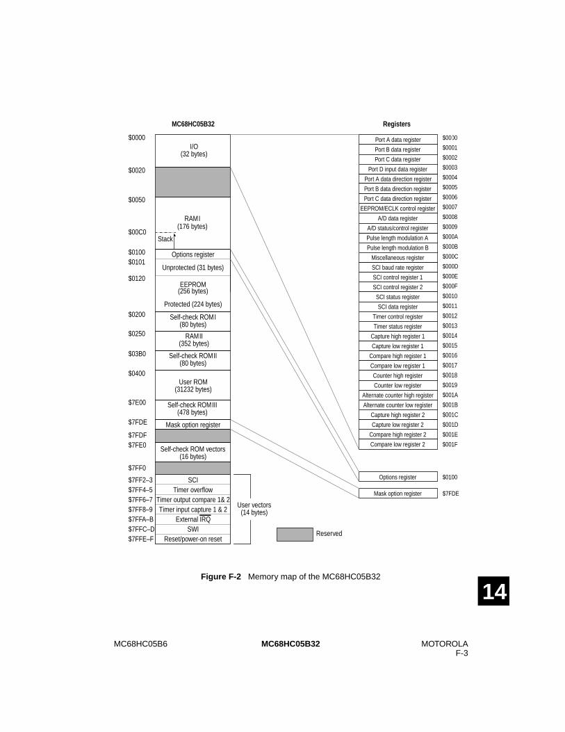
MC68HC05B6 MOTOROLAF-3
MC68HC05B32
14Figure F-2 Memory map of the MC68HC05B32
Port B data register
Port C data register
Port D input data register
Port A data register $0000
Compare low register 2
A/D data register
$0000I/O
(32 bytes)
$0020
$00C0
$0100
$7FDF
$7FF0
Stack
RAMI(176 bytes)
$0250
$0200
$0050
Port A data direction register
Port B data direction register
Port C data direction register
EEPROM/ECLK control register
A/D status/control register
Pulse length modulation A
Pulse length modulation B
Miscellaneous register
SCI baud rate register
SCI control register 1
SCI control register 2
SCI status register
SCI data register
Timer control register
Timer status register
Capture high register 1
Capture low register 1
Compare high register 1
Compare low register 1
Counter high register
Counter low register
Alternate counter high register
Alternate counter low register
Capture high register 2
Capture low register 2
Compare high register 2
$0001
$0002
$0003
$0004
$0005
$0006
$0007
$0008
$0009
$000A
$000B
$000C
$000D
$000E
$000F
$0010
$0011
$0012
$0013
$0014
$0015
$0016
$0017
$0018
$0019
$001A
$001B
$001C
$001D
$001E
$001F
User ROM(31232 bytes)
Self-check ROMIII(478 bytes)
$03B0
$7FE0
Options register
Unprotected (31 bytes)
Protected (224 bytes)
EEPROM(256 bytes)
$0101
$0120
$0100Options register
Reserved
MC68HC05B32 Registers
RAMII(352 bytes)
$0400
Mask option register
Mask option register $7FDE
Self-check ROMI(80 bytes)
Self-check ROM vectors(16 bytes)
Self-check ROMII(80 bytes)
$7E00
$7FDE
User vectors(14 bytes)
$7FF2–3 SCITimer overflow
Timer output compare 1& 2Timer input capture 1 & 2
External IRQSWI
Reset/power-on reset
$7FF4–5$7FF6–7$7FF8–9$7FFA–B$7FFC–D$7FFE–F

MOTOROLAF-4
MC68HC05B6MC68HC05B32
14
(1) This bit is set each time there is a power-on reset.
(2) The state of the WDOG bit after reset is dependent upon the mask option selected; 1 = watchdog enabled, 0 = watchdog disabled.
(3) This register is implemented in EEPROM; therefore reset has no effect on the individual bits.
(4) This register is implemented in ROM; therefore reset has no effect on the individual bits.
Table F-1 Register outline
Register name Address bit 7 bit 6 bit 5 bit 4 bit 3 bit 2 bit 1 bit 0State on
reset
Port A data (PORTA) $0000 Undefined
Port B data (PORTB) $0001 Undefined
Port C data (PORTC) $0002 PC2/ECLK
Undefined
Port D data (PORTD) $0003 PD7 PD6 PD5 PD4 PD3 PD2 PD1 PD0 Undefined
Port A data direction (DDRA) $0004 0000 0000
Port B data direction (DDRB) $0005 0000 0000
Port C data direction (DDRC) $0006 0000 0000
EEPROM/ECLK control $0007 0 0 0 0 ECLK E1ERA E1LAT E1PGM 0000 0000
A/D data (ADDATA) $0008 0000 0000
A/D status/control (ADSTAT) $0009 COCO ADRC ADON 0 CH3 CH2 CH1 CH0 0000 0000
Pulse length modulation A (PLMA) $000A 0000 0000
Pulse length modulation B (PLMB) $000B 0000 0000
Miscellaneous $000C POR(1) INTP INTN INTE SFA SFB SM WDOG(2) ?001 000?
SCI baud rate (BAUD) $000D SPC1 SPC0 SCT1 SCT0 SCT0 SCR2 SCR1 SCR0 00uu uuuu
SCI control 1 (SCCR1) $000E R8 T8 M WAKE CPOL CPHA LBCL Undefined
SCI control 2 (SCCR2) $000F TIE TCIE RIE ILIE TE RE RWU SBK 0000 0000
SCI status (SCSR) $0010 TDRE TC RDRF IDLE OR NF FE 1100 000u
SCI data (SCDR) $0011 0000 0000
Timer control (TCR) $0012 ICIE OCIE TOIE FOLV2 FOLV1 OLV2 IEDG1 OLVL1 0000 00u0
Timer status (TSR) $0013 ICF1 OCF1 TOF ICF2 OCF2 Undefined
Input capture high 1 $0014 Undefined
Input capture low 1 $0015 Undefined
Output compare high 1 $0016 Undefined
Output compare low 1 $0017 Undefined
Timer counter high $0018 1111 1111
Timer counter low $0019 1111 1100
Alternate counter high $001A 1111 1111
Alternate counter low $001B 1111 1100
Input capture high 2 $001C Undefined
Input capture low 2 $001D Undefined
Output compare high 2 $001E Undefined
Output compare low 2 $001F Undefined
Options (OPTR)(3) $0100 EE1P SEC Not affected
Mask option register (MOR)(4) $7FDE RTIM RWAT WWAT PBPD PCPD Not affected
MC68HC05B6 MOTOROLAG-1
MC68HC705B32
14
GMC68HC705B32
The MC68HC705B32 is an EPROM version of the MC68HC05B32, with the ROM replaced by asimilar amount of EPROM and with a bootstrap mode instead of a self-check mode. The entireMC68HC05B6 data sheet applies to the MC68HC705B32, with the exceptions outlined in thisappendix.
Features
• 31248 bytes user EPROM
• No page zero EPROM at $20–$4F
• 528 bytes of RAM
• 638 bytes bootstrap ROM instead of 432 bytes of self-check ROM
• Simultaneous programming of up to 16 bytes of EPROM
• 52-pin PLCC, 56-pin SDIP and 64-pin QFP packages
Note: The electrical characteristics from the MC68HC05B6 data sheet should not be used forthe MC68HC705B32. Data specific to this device can be found in Section G.2.6 andSection G.2.8.
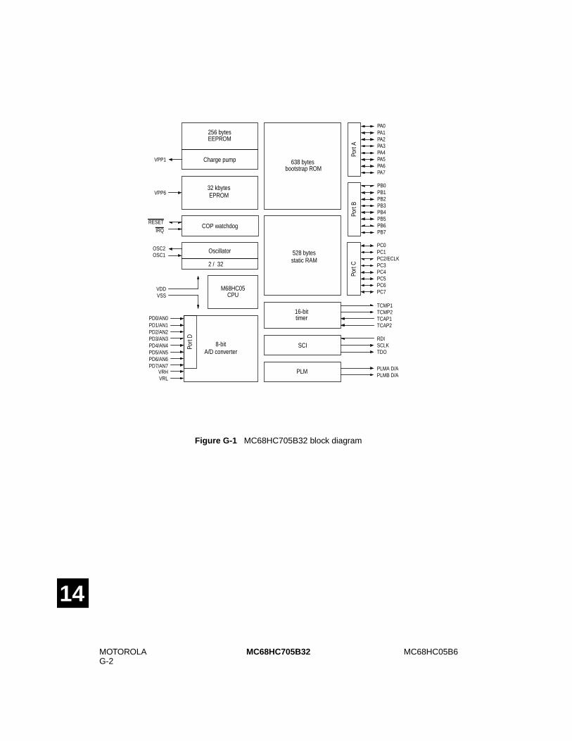
MOTOROLAG-2
MC68HC05B6MC68HC705B32
14
Figure G-1 MC68HC705B32 block diagram
Port
A
PA0PA1PA2PA3PA4PA5PA6PA7
Port
B
PB0PB1PB2PB3PB4PB5PB6PB7
Port
C
PC0PC1PC2/ECLKPC3PC4PC5PC6PC7
16-bittimer
Port
D
PD0/AN0PD1/AN1PD2/AN2PD3/AN3PD4/AN4PD5/AN5PD6/AN6PD7/AN7
Oscillator
COP watchdogRESET
IRQ
VDDVSS
OSC1OSC2
M68HC05CPU
SCIA/D converter
PLM
TCAP1TCAP2
TCMP1TCMP2
VRHVRL
RDISCLKTDO
VPP1
256 bytesEEPROM
Charge pump
2 / 32
PLMA D/APLMB D/A
8-bit
32 kbytesEPROM
528 bytesstatic RAM
638 bytes
VPP6
bootstrap ROM
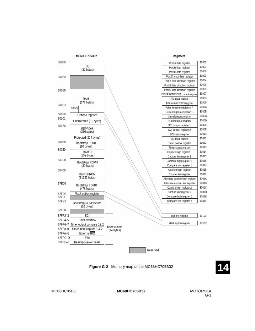
MC68HC05B6 MOTOROLAG-3
MC68HC705B32
14Figure G-2 Memory map of the MC68HC705B32
Port B data register
Port C data register
Port D input data register
Port A data register $0000
Compare low register 2
A/D data register
$0000I/O
(32 bytes)
$0020
$00C0
$0100
$7FDE
$7FF0
Stack
RAM1(176 bytes)
$0250
$0200
$0050
Port A data direction register
Port B data direction register
Port C data direction register
E/EEPROM/ECLK control register
A/D status/control register
Pulse length modulation A
Pulse length modulation B
Miscellaneous register
SCI baud rate register
SCI control register 1
SCI control register 2
SCI status register
SCI data register
Timer control register
Timer status register
Capture high register 1
Capture low register 1
Compare high register 1
Compare low register 1
Counter high register
Counter low register
Alternate counter high register
Alternate counter low register
Capture high register 2
Capture low register 2
Compare high register 2
$0001
$0002
$0003
$0004
$0005
$0006
$0007
$0008
$0009
$000A
$000B
$000C
$000D
$000E
$000F
$0010
$0011
$0012
$0013
$0014
$0015
$0016
$0017
$0018
$0019
$001A
$001B
$001C
$001D
$001E
$001F
Bootstrap ROMII(80 bytes)
Bootstrap ROM vectors(16 bytes)
$03B0
$7FE0
Options register
Unprotected (31 bytes)
Protected (224 bytes)
EEPROM(256 bytes)
$0101
$0120
$0100Options register
Reserved
MC68HC705B32 Registers
RAM11(352 bytes)
$0400
Mask option register
Mask option register $7FDE
Bootstrap ROMI(80 bytes)
User EPROM(31232 bytes)
Bootstrap ROMIII(478 bytes)
$7E00
User vectors(14 bytes)
$7FF2–3 SCITimer overflow
Timer output compare 1& 2Timer input capture 1 & 2
External IRQSWI
Reset/power-on reset
$7FDF
$7FF4–5$7FF6–7$7FF8–9$7FFA–B$7FFC–D$7FFE–F
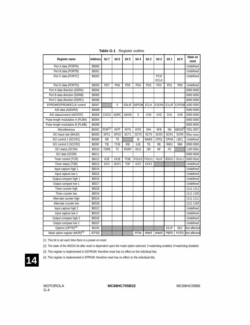
MOTOROLAG-4
MC68HC05B6MC68HC705B32
14
(1) This bit is set each time there is a power-on reset.
(2) The state of the WDOG bit after reset is dependent upon the mask option selected; 1=watchdog enabled, 0=watchdog disabled.
(3) This register is implemented in EEPROM; therefore reset has no effect on the individual bits.
(4) This register is implemented in EPROM; therefore reset has no effect on the individual bits.
Table G-1 Register outline
Register name Address bit 7 bit 6 bit 5 bit 4 bit 3 bit 2 bit 1 bit 0State on
reset
Port A data (PORTA) $0000 Undefined
Port B data (PORTB) $0001 Undefined
Port C data (PORTC) $0002 PC2/ECLK
Undefined
Port D data (PORTD) $0003 PD7 PD6 PD5 PD4 PD3 PD2 PD1 PD0 Undefined
Port A data direction (DDRA) $0004 0000 0000
Port B data direction (DDRB) $0005 0000 0000
Port C data direction (DDRC) $0006 0000 0000
EPROM/EEPROM/ECLK control $0007 0 E6LAT E6PGM ECLK E1ERA E1LAT E1PGM u000 0000
A/D data (ADDATA) $0008 0000 0000
A/D status/control (ADSTAT) $0009 COCO ADRC ADON 0 CH3 CH2 CH1 CH0 0000 0000
Pulse length modulation A (PLMA) $000A 0000 0000
Pulse length modulation B (PLMB) $000B 0000 0000
Miscellaneous $000C POR(1) INTP INTN INTE SFA SFB SM WDOG(2) ?001 000?
SCI baud rate (BAUD) $000D SPC1 SPC0 SCT1 SCT0 SCT0 SCR2 SCR1 SCR0 00uu uuuu
SCI control 1 (SCCR1) $000E R8 T8 M WAKE CPOL CPHA LBCL Undefined
SCI control 2 (SCCR2) $000F TIE TCIE RIE ILIE TE RE RWU SBK 0000 0000
SCI status (SCSR) $0010 TDRE TC RDRF IDLE OR NF FE 1100 000u
SCI data (SCDR) $0011 0000 0000
Timer control (TCR) $0012 ICIE OCIE TOIE FOLV2 FOLV1 OLV2 IEDG1 OLVL1 0000 00u0
Timer status (TSR) $0013 ICF1 OCF1 TOF ICF2 OCF2 Undefined
Input capture high 1 $0014 Undefined
Input capture low 1 $0015 Undefined
Output compare high 1 $0016 Undefined
Output compare low 1 $0017 Undefined
Timer counter high $0018 1111 1111
Timer counter low $0019 1111 1100
Alternate counter high $001A 1111 1111
Alternate counter low $001B 1111 1100
Input capture high 2 $001C Undefined
Input capture low 2 $001D Undefined
Output compare high 2 $001E Undefined
Output compare low 2 $001F Undefined
Options (OPTR)(3) $0100 EE1P SEC Not affected
Mask option register (MOR)(4) $7FDE RTIM RWAT WWAT PBPD PCPD Not affected
MC68HC05B6 MOTOROLAG-5
MC68HC705B32
14
G.1 EPROM
Figure G-2 shows the MC68HC705B32 memory map. The device has a total of 31232 bytes ofEPROM (including 14 bytes for User vectors) and 256 bytes of EEPROM.
The EPROM array is supplied by the VPP6 pin in both read and program modes. Typically theuser’s software will be loaded into a programming board where VPP6 is controlled by one of thebootstrap loader routines. It will then be placed in an application where no programming occurs.In this case the VPP6 pin should be hardwired to VDD.
Warning: A minimum VDD voltage must be applied to the VPP6 pin at all times, includingpower-on. Failure to do so could result in permanent damage to the device.
G.1.1 EPROM read operation
The execution of a program in the EPROM address range or a load from the EPROM are bothread operations. The E6LAT bit in the EPROM/EEPROM control register should be cleared to ‘0’which automatically resets the E6PGM bit. In this way the EPROM is read like a normal ROM.Reading the EPROM with the E6LAT bit set will give data that does not correspond to the actualmemory content. As interrupt vectors are in EPROM, they will not be loaded when E6LAT is set.Similarly, the bootstrap ROM routines cannot be executed when E6LAT is set. In read mode, theVPP6 pin must be at the VDD level. When entering the STOP mode, the EPROM is automaticallyset to the read mode.
Note: An erased byte reads as $00.
G.1.2 EPROM program operation
Typically, the EPROM will be programmed by the bootstrap routines resident in the on-chip ROM.However, the user program can be used to program some EPROM locations if the properprocedure is followed. In particular, the programming sequence must be running in RAM, as theEPROM will not be available for code execution while the E6LAT bit is set. The VPP6 switchingmust occur externally after EPGM is set, for example under control of a signal generated on a pinby the programming routine.
Note: When the part becomes a PROM, only the cumulative programming of bits to logic ‘1’is possible if multiple programming is made on the same byte.
To allow simultaneous programming of up to sixteen bytes, these bytes must be in the same groupof addresses which share the same most significant address bits; only the four LSBs can change.
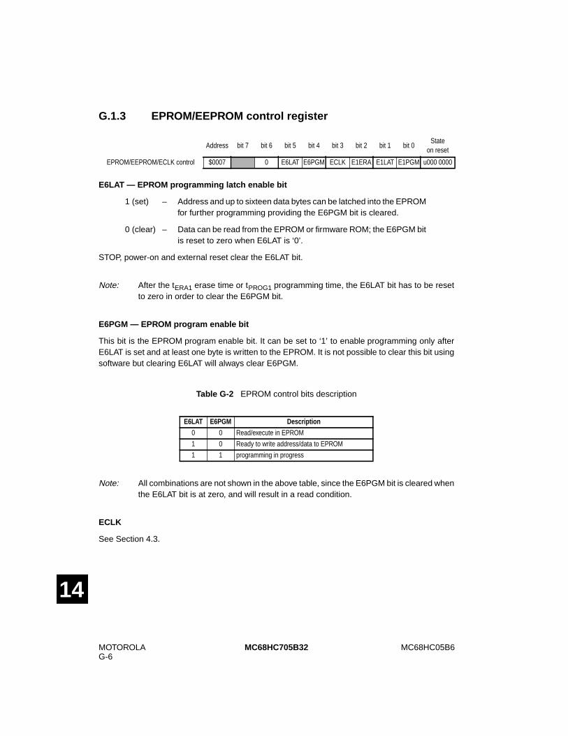
MOTOROLAG-6
MC68HC05B6MC68HC705B32
14
G.1.3 EPROM/EEPROM control register
E6LAT — EPROM programming latch enable bit
1 (set) – Address and up to sixteen data bytes can be latched into the EPROMfor further programming providing the E6PGM bit is cleared.
0 (clear) – Data can be read from the EPROM or firmware ROM; the E6PGM bitis reset to zero when E6LAT is ‘0’.
STOP, power-on and external reset clear the E6LAT bit.
Note: After the tERA1 erase time or tPROG1 programming time, the E6LAT bit has to be resetto zero in order to clear the E6PGM bit.
E6PGM — EPROM program enable bit
This bit is the EPROM program enable bit. It can be set to ‘1’ to enable programming only afterE6LAT is set and at least one byte is written to the EPROM. It is not possible to clear this bit usingsoftware but clearing E6LAT will always clear E6PGM.
Note: All combinations are not shown in the above table, since the E6PGM bit is cleared whenthe E6LAT bit is at zero, and will result in a read condition.
ECLK
See Section 4.3.
Address bit 7 bit 6 bit 5 bit 4 bit 3 bit 2 bit 1 bit 0State
on reset
EPROM/EEPROM/ECLK control $0007 0 E6LAT E6PGM ECLK E1ERA E1LAT E1PGM u000 0000
Table G-2 EPROM control bits description
E6LAT E6PGM Description
0 0 Read/execute in EPROM
1 0 Ready to write address/data to EPROM
1 1 programming in progress
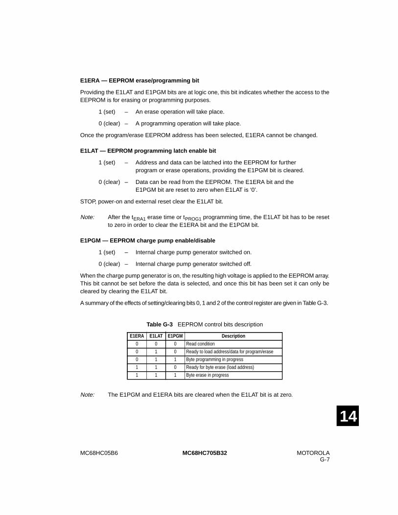
MC68HC05B6 MOTOROLAG-7
MC68HC705B32
14
E1ERA — EEPROM erase/programming bit
Providing the E1LAT and E1PGM bits are at logic one, this bit indicates whether the access to theEEPROM is for erasing or programming purposes.
1 (set) – An erase operation will take place.
0 (clear) – A programming operation will take place.
Once the program/erase EEPROM address has been selected, E1ERA cannot be changed.
E1LAT — EEPROM programming latch enable bit
1 (set) – Address and data can be latched into the EEPROM for furtherprogram or erase operations, providing the E1PGM bit is cleared.
0 (clear) – Data can be read from the EEPROM. The E1ERA bit and theE1PGM bit are reset to zero when E1LAT is ‘0’.
STOP, power-on and external reset clear the E1LAT bit.
Note: After the tERA1 erase time or tPROG1 programming time, the E1LAT bit has to be resetto zero in order to clear the E1ERA bit and the E1PGM bit.
E1PGM — EEPROM charge pump enable/disable
1 (set) – Internal charge pump generator switched on.
0 (clear) – Internal charge pump generator switched off.
When the charge pump generator is on, the resulting high voltage is applied to the EEPROM array.This bit cannot be set before the data is selected, and once this bit has been set it can only becleared by clearing the E1LAT bit.
A summary of the effects of setting/clearing bits 0, 1 and 2 of the control register are given in Table G-3.
Note: The E1PGM and E1ERA bits are cleared when the E1LAT bit is at zero.
Table G-3 EEPROM control bits description
E1ERA E1LAT E1PGM Description
0 0 0 Read condition
0 1 0 Ready to load address/data for program/erase
0 1 1 Byte programming in progress
1 1 0 Ready for byte erase (load address)
1 1 1 Byte erase in progress
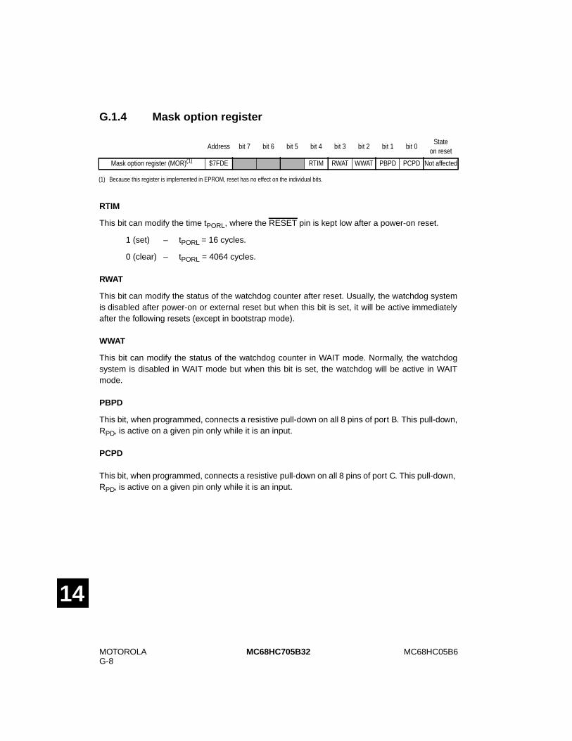
MOTOROLAG-8
MC68HC05B6MC68HC705B32
14
G.1.4 Mask option register
RTIM
This bit can modify the time tPORL, where the RESET pin is kept low after a power-on reset.
1 (set) – tPORL = 16 cycles.
0 (clear) – tPORL = 4064 cycles.
RWAT
This bit can modify the status of the watchdog counter after reset. Usually, the watchdog systemis disabled after power-on or external reset but when this bit is set, it will be active immediatelyafter the following resets (except in bootstrap mode).
WWAT
This bit can modify the status of the watchdog counter in WAIT mode. Normally, the watchdogsystem is disabled in WAIT mode but when this bit is set, the watchdog will be active in WAITmode.
PBPD
This bit, when programmed, connects a resistive pull-down on all 8 pins of port B. This pull-down,RPD, is active on a given pin only while it is an input.
PCPD
This bit, when programmed, connects a resistive pull-down on all 8 pins of port C. This pull-down,RPD, is active on a given pin only while it is an input.
(1) Because this register is implemented in EPROM, reset has no effect on the individual bits.
Address bit 7 bit 6 bit 5 bit 4 bit 3 bit 2 bit 1 bit 0State
on reset
Mask option register (MOR)(1) $7FDE RTIM RWAT WWAT PBPD PCPD Not affected
MC68HC05B6 MOTOROLAG-9
MC68HC705B32
14
G.1.5 Options register (OPTR)
EE1P – EEPROM protect bit
In order to achieve a higher degree of protection, the EEPROM is effectively split into two parts,both working from the VPP1 charge pump. Part 1 of the EEPROM array (32 bytes from $0100 to$011F) cannot be protected; part 2 (224 bytes from $0120 to $01FF) is protected by the EE1P bitof the options register.
1 (set) – Part 2 of the EEPROM array is not protected; all 256 bytes ofEEPROM can be accessed for any read, erase or programmingoperations.
0 (clear) – Part 2 of the EEPROM array is protected; any attempt to erase orprogram a location will be unsuccessful.
When this bit is set to 1 (erased), the protection will remain until the next power-on or externalreset. EE1P can only be written to ‘0’ when the E1LAT bit in the EEPROM control register is set.
Note: The EEPROM1 protect function is disabled while in bootstrap mode.
SEC — Secure bit
This bit allows the EPROM and EEPROM1 to be secured from external access. When this bit isin the erased state (set), the EPROM and EEPROM1 content is not secured and the device maybe used in non user mode. When the SEC bit is programmed to ‘zero’, the EPROM andEEPROM1 content is secured by prohibiting entry to the non user mode. To deactivate the securebit, the EPROM has to be erased by exposure to a high density ultraviolet light, and the device hasto be entered into the EPROM erase verification mode with PD1 set. When the SEC bit ischanged, its new value will have no effect until the next power-on or external reset.
1 (set) – EEPROM/EPROM not protected.
0 (clear) – EEPROM/EPROM protected.
(1) Because this register is implemented in EEPROM, reset has no effect on the individual bits.
Address bit 7 bit 6 bit 5 bit 4 bit 3 bit 2 bit 1 bit 0State
on reset
Options (OPTR)(1) $0100 EE1P SEC Not affected
MOTOROLAG-10
MC68HC05B6MC68HC705B32
14
G.2 Bootstrap mode
The 432 bytes of self-check firmware on the MC68HC05B6 are replaced by 654 bytes of bootstrapfirmware. A detailed description of the modes of operation within bootstrap mode is given below.
The bootstrap program in mask ROM address locations $0200 to $024F, $03B0 to $3FFF, $7E00to $7FDD and $7FE0 to $7FEF can be used to program the EPROM and the EEPROM, to checkif the EPROM is erased or to load and execute data in RAM.
After reset, while going to the bootstrap mode, the vector located at address $7FEE and $7FEF(RESET) is fetched to start execution of the bootstrap program. To place the part in bootstrapmode, the IRQ pin should be at 2xVDD with the TCAP1 pin ‘high’ during transition of the RESETpin from low to high. The hold time on the IRQ and TCAP1 pins is two clock cycles after theexternal RESET pin is brought high.
When the MC68HC705B32 is placed in the bootstrap mode, the bootstrap reset vector will befetched and the bootstrap firmware will start to execute. Table G-4 shows the conditions requiredto enter each level of bootstrap mode on the rising edge of RESET.
The bootstrap program will first copy part of itself in RAM (except ‘RAM parallel load’), as theprogram cannot be executed in ROM during verification/programming of the EPROM. It will thenset the TCMP1 output to a logic high level, unlike the MC68HC05B6 which keeps TCMP1 low. Thiscan be used to distinguish between the two circuits and, in particular, for selection of the VPP leveland current capability.
Table G-4 Mode of operation selection
IRQ pin TCAP1 pin PD1 PD2 PD3 PD4 Mode
VSS to VDD VSS to VDD x x x x Single chip
+ 9 Volts VDD 0 0 0 x Erased EPROM verification
+ 9 Volts VDD 1 0 0 0Erased EPROM verification; erase EEPROM;EPROM/EEPROM parallel program/verify
+ 9 Volts VDD 0 1 0 0Erased EPROM verification;no EEPROM erase if SEC is zero (parallel mode)
+ 9 Volts VDD 1 1 0 0Erased EPROM verification; erase EEPROM;EPROM parallel program/verify (no E2)
+ 9 Volts VDD x 1 1 0 Jump to start of RAM ($0051); SEC bit = 0
+ 9 Volts VDD 0 1 0 1 EPROM and EEPROM verification; SEC bit = 0 (parallel mode)
+ 9 Volts VDD x x 1 1Serial RAM load/execute – similar to MC68HC05B6 but can fill RAMI, II and III
x = Don’t care
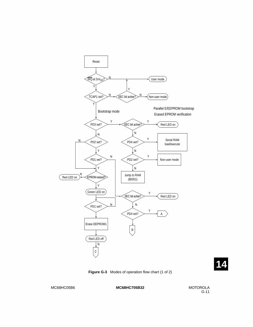
MC68HC05B6 MOTOROLAG-11
MC68HC705B32
14Figure G-3 Modes of operation flow chart (1 of 2)
Red LED on
TCAP1 set?
SEC bit active?PD3 set?
Reset
User mode
Red LED on
Non-user mode
Non-user modeN
YY
Y
Y
N
Y
N
N
Bootstrap modeParallel E/EEPROM bootstrap
N
PD4 set?
Y
Erased EPROM verification
Serial RAMload/execute
N
PD2 set?
Y
N
Jump to RAM($0051)
PD2 set?
N
PD1 set?
Y
N
SEC bit active? Red LED onY
N
PD4 set?Y
EPROM erased?
N
Y
Y
Green LED on
PD1 set?
N
Erase EEPROM1
Red LED off
N
A
B
C
SEC bit active?
IRQ at 2xVDD?
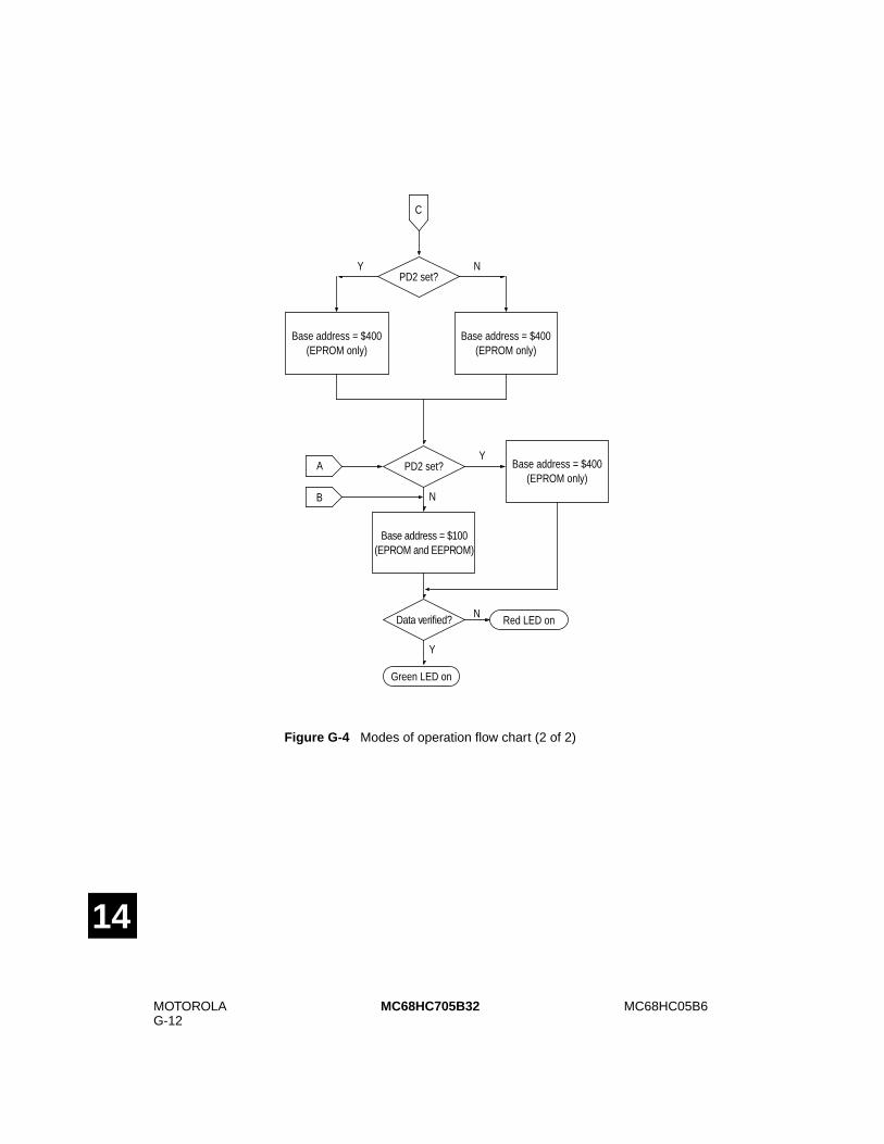
MOTOROLAG-12
MC68HC05B6MC68HC705B32
14
Figure G-4 Modes of operation flow chart (2 of 2)
Data verified?
YPD2 set?
NN
Red LED on
A Base address = $400(EPROM only)
Base address = $100(EPROM and EEPROM)
Y
N
Green LED on
B
C
PD2 set?NY
Base address = $400(EPROM only)
Base address = $400(EPROM only)
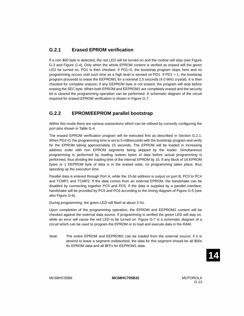
MC68HC05B6 MOTOROLAG-13
MC68HC705B32
14
G.2.1 Erased EPROM verification
If a non $00 byte is detected, the red LED will be turned on and the routine will stop (see FigureG-3 and Figure G-4). Only when the whole EPROM content is verified as erased will the greenLED be turned on. PD1 is then checked. If PD1=0, the bootstrap program stops here and noprogramming occurs until such time as a high level is sensed on PD1. If PD1 = 1, the bootstrapprogram proceeds to erase the EEPROM1 for a nominal 2.5 seconds (4.0 MHz crystal). It is thenchecked for complete erasure; if any EEPROM byte is not erased, the program will stop beforeerasing the SEC byte. When both EPROM and EEPROM1 are completely erased and the securitybit is cleared the programming operation can be performed. A schematic diagram of the circuitrequired for erased EPROM verification is shown in Figure G-7.
G.2.2 EPROM/EEPROM parallel bootstrap
Within this mode there are various subsections which can be utilised by correctly configuring theport pins shown in Table G-4.
The erased EPROM verification program will be executed first as described in Section G.2.1.When PD2=0, the programming time is set to 5 milliseconds with the bootstrap program and verifyfor the EPROM taking approximately 15 seconds. The EPROM will be loaded in increasingaddress order with non EPROM segments being skipped by the loader. Simultaneousprogramming is performed by reading sixteen bytes of data before actual programming isperformed, thus dividing the loading time of the internal EPROM by 16. If any block of 16 EPROMbytes or 1 EEPROM byte of data is in the erased state, no programming takes place, thusspeeding up the execution time.
Parallel data is entered through Port A, while the 15-bit address is output on port B, PC0 to PC4and TCMP1 and TCMP2. If the data comes from an external EPROM, the handshake can bedisabled by connecting together PC5 and PC6. If the data is supplied by a parallel interface,handshake will be provided by PC5 and PC6 according to the timing diagram of Figure G-5 (seealso Figure G-6).
During programming, the green LED will flash at about 3 Hz.
Upon completion of the programming operation, the EPROM and EEPROM1 content will bechecked against the external data source. If programming is verified the green LED will stay on,while an error will cause the red LED to be turned on. Figure G-7 is a schematic diagram of acircuit which can be used to program the EPROM or to load and execute data in the RAM.
Note: The entire EPROM and EEPROM1 can be loaded from the external source; if it isdesired to leave a segment undisturbed, the data for this segment should be all $00sfor EPROM data and all $FFs for EEPROM1 data.
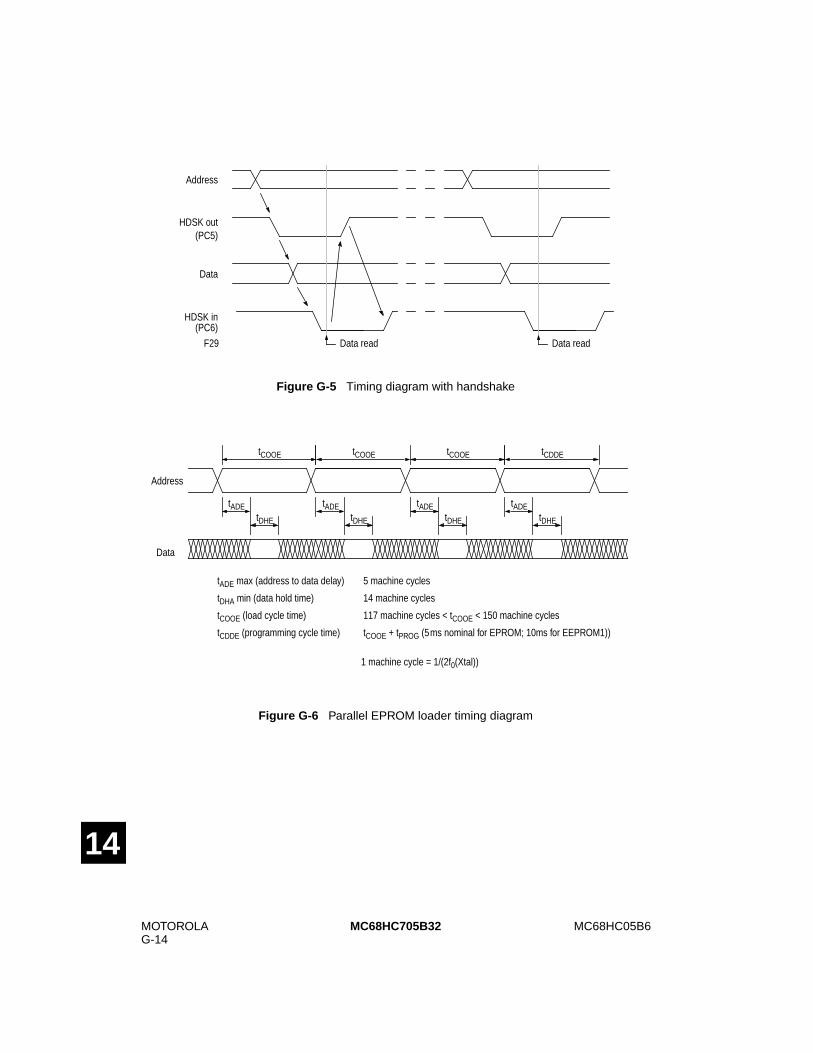
MOTOROLAG-14
MC68HC05B6MC68HC705B32
14
Figure G-5 Timing diagram with handshake
Figure G-6 Parallel EPROM loader timing diagram
Data read Data read
Address
HDSK out(PC5)
Data
HDSK in(PC6)
F29
tCOOE
tADEtDHE
Address
Data
tADEtDHE
tADEtDHE
tADEtDHE
tCOOE tCOOE tCDDE
tADE max (address to data delay) 5 machine cycles
tDHA min (data hold time) 14 machine cycles
tCOOE (load cycle time) 117 machine cycles < tCOOE < 150 machine cycles
tCDDE (programming cycle time) tCOOE + tPROG (5ms nominal for EPROM; 10ms for EEPROM1))
1 machine cycle = 1/(2f0(Xtal))
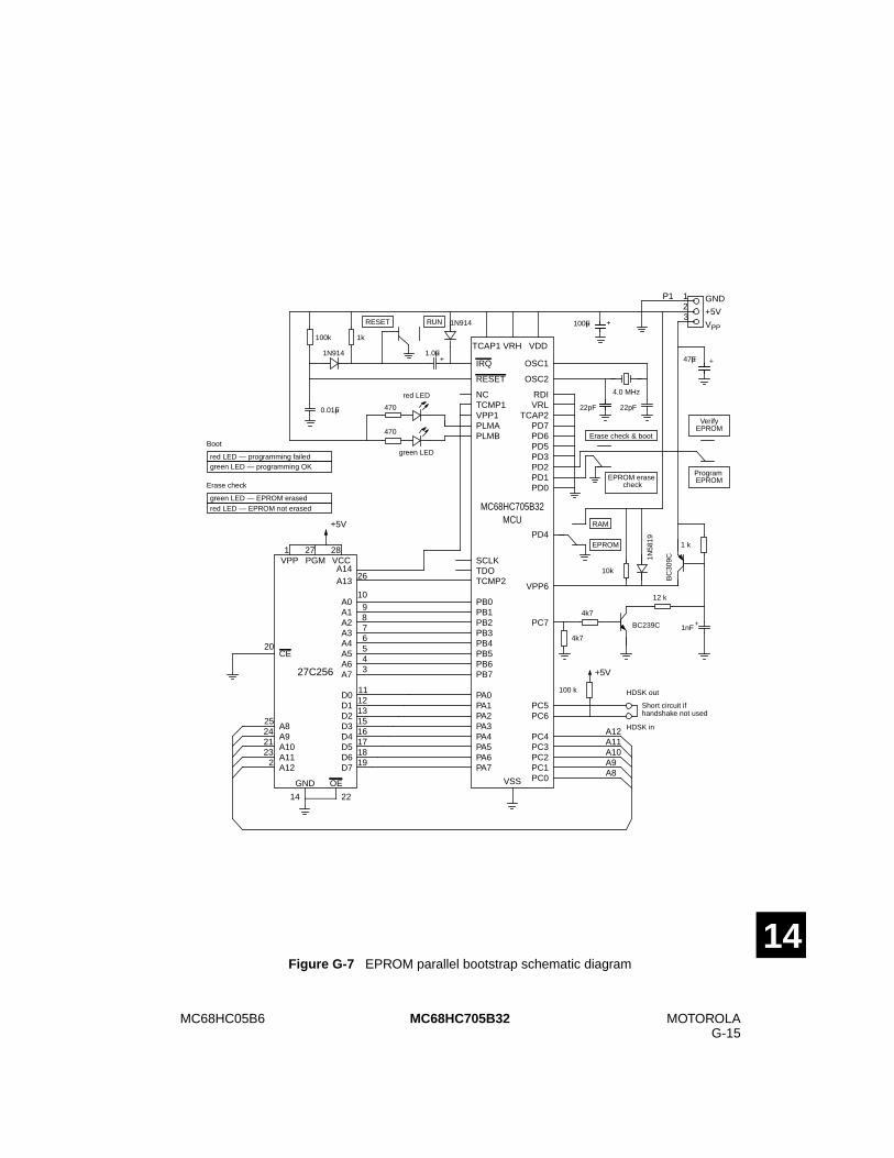
MC68HC05B6 MOTOROLAG-15
MC68HC705B32
14Figure G-7 EPROM parallel bootstrap schematic diagram
VCC281
VPP PGM27
PB0PB1PB2PB3PB4PB5PB6PB7
PA0PA1PA2PA3PA4PA5PA6PA7
VDD
OSC1
OSC2
TCAP1
IRQ
RESET
VSS
A0A1A2A3A4A5A6A7
D0D1D2D3D4D5D6D7
GND OE
14 22
10987654
26
12131516171819
11
3
+5V
12
P1 GND
+5V100µF
22pF
4.0 MHz
1N914
1k½
1.0µF
22pF
100k½
1N914
RESET RUN
0.01µF
TDOSCLK
RDIVRL
TCAP2PD7PD6PD5PD3PD2PD1PD0
PD4
+5V
3VPP
VPP6
PC7
PC5
PC4PC3PC2PC1PC0
PC6
242123
2
A9A8
A10
A12
CE
A11
A12A11A10A9A8
HDSK out
HDSK in
Short circuit ifhandshake not used
100 k½
NCTCMP1
TCMP2
PLMAPLMB
470½
470½
red LED
green LED
4k7½
4k7½
12 k½
BC239C
BC
309C
10k ½
27C256
+
+
VRH
red LED — programming failedgreen LED — programming OK
25
1nF
1N58
19
1 k½
+
RAM
EPROM
green LED — EPROM erased
47µF +
Erase check & boot
EPROM erase check
VPP1
red LED — EPROM not erased
Boot
Erase check
A13
20
MC68HC705B32MCU
A14
Verify
ProgramEPROM
EPROM
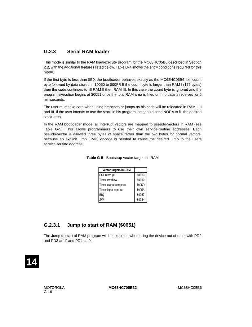
MOTOROLAG-16
MC68HC05B6MC68HC705B32
14
G.2.3 Serial RAM loader
This mode is similar to the RAM load/execute program for the MC68HC05B6 described in Section2.2, with the additional features listed below. Table G-4 shows the entry conditions required for thismode.
If the first byte is less than $B0, the bootloader behaves exactly as the MC68HC05B6, i.e. countbyte followed by data stored in $0050 to $00FF. If the count byte is larger than RAM I (176 bytes)then the code continues to fill RAM II then RAM III. In this case the count byte is ignored and theprogram execution begins at $0051 once the total RAM area is filled or if no data is received for 5milliseconds.
The user must take care when using branches or jumps as his code will be relocated in RAM I, IIand III. If the user intends to use the stack in his program, he should send NOP’s to fill the desiredstack area.
In the RAM bootloader mode, all interrupt vectors are mapped to pseudo-vectors in RAM (seeTable G-5). This allows programmers to use their own service-routine addresses. Eachpseudo-vector is allowed three bytes of space rather than the two bytes for normal vectors,because an explicit jump (JMP) opcode is needed to cause the desired jump to the usersservice-routine address.
G.2.3.1 Jump to start of RAM ($0051)
The Jump to start of RAM program will be executed when bring the device out of reset with PD2and PD3 at ‘1’ and PD4 at ‘0’.
Table G-5 Bootstrap vector targets in RAM
Vector targets in RAM
SCI interrupt $0063
Timer overflow $0060
Timer output compare $005D
Timer input capture $005A
IRQ $0057
SWI $0054
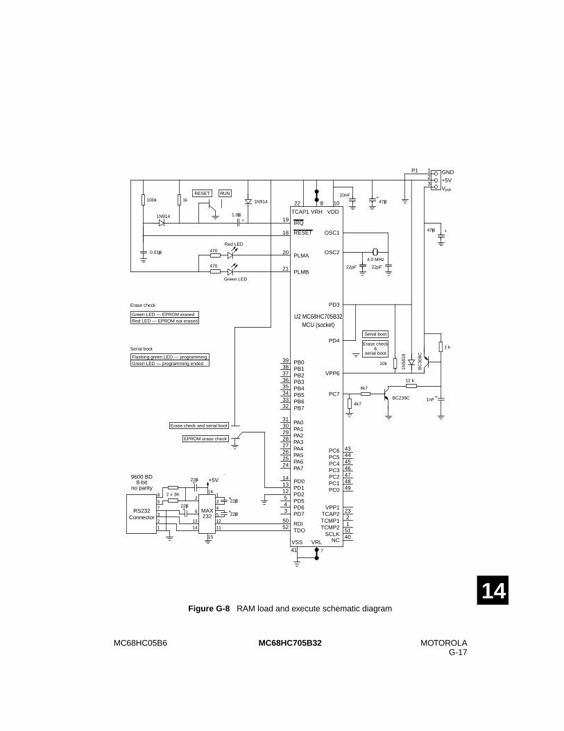
MC68HC05B6 MOTOROLAG-17
MC68HC705B32
14Figure G-8 RAM load and execute schematic diagram
Green LED — programming endedFlashing green LED — programming
40
VPP6
PC7
PB0PB1PB2PB3PB4PB5PB6PB7
PA0PA1PA2PA3PA4PA5PA6PA7
VDD
OSC1
OSC2
TCAP1
IRQ
RESET
VSS
12
P1 GND
+5V
1N9141k½
1.0µF
100k½
1N914
RESET RUN
0.01µF
3VPP
PC5PC4PC3PC2PC1PC0
PC6
PLMA
PLMB
470½
470½
Red LED
Green LED
+
+
VRH
22µF
22µF
22µF
2 x 3K½ 12
34
8
675
111213
14
15
16
5321
22µF
RS232Connector
MAX232
+5V9600 BD
8-bitno parity
19
18
20
21
5052
3938373635343332
3130292827262524
14131254
43444546474849
232151
22 8 10
41 7
VRL
TCAP2TCMP1TCMP2
SCLKNC
10nF47µF
PD0
PD4
PD1PD2PD5PD6PD7
+
+
+
+
22pF
4.0 MHz
22pF
4k7½
4k7½
12 k½
BC239C
BC
309C
10k ½
1nF1N
5819
1 k½
+
Serial boot
Erase check
47µF +
PD3
RDITDO
Erase check
Red LED — EPROM not erasedGreen LED — EPROM erased
Serial boot &serial boot
Erase check and serial boot
EPROM erase check
VPP13
U2 MC68HC705B32MCU (socket)
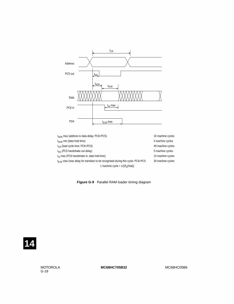
MOTOROLAG-18
MC68HC05B6MC68HC705B32
14
Figure G-9 Parallel RAM loader timing diagram
tADR tDHR
Address
Data
tCR
PD4 tEXR max
tHO
tHI max
PC5 out
PC6 in
tADR max (address to data delay; PC6=PC5) 16 machine cycles
tDHR min (data hold time) 4 machine cycles
tCR (load cycle time; PC6=PC5) 49 machine cycles
tHO (PC5 handshake out delay) 5 machine cycles
tHI max (PC6 handshake in, data hold time) 10 machine cycles
tEXR max (max delay for transition to be recognised during this cycle; PC6=PC5 30 machine cycles
1 machine cycle = 1/(2f0(Xtal))

MC68HC05B6 MOTOROLAG-19
MC68HC705B32
14
G.2.4 Maximum ratings
Note: This device contains circuitry designed to protect against damage due to highelectrostatic voltages or electric fields. However, it is recommended that normalprecautions be taken to avoid the application of any voltages higher than those givenin the maximum ratings table to this high impedance circuit. For maximum reliability allunused inputs should be tied to either VSS or VDD.
(1) All voltages are with respect to VSS.
(2) Maximum current drain per pin is for one pin at a time, limited by an external resistor.
Table G-6 Maximum ratings
Rating Symbol Value Unit
Supply voltage(1) VDD – 0.5 to +7.0 V
Input voltage VIN VSS – 0.5 to VDD + 0.5 V
Input voltage– Self-check mode (IRQ pin only)
VIN VSS – 0.5 to 2VDD + 0.5 V
Operating temperature range– Standard (MC68HC705B32)– Extended (MC68HC705B32C)– Industrial (MC68HC705B32V)– Automotive (MC68HC705B32M)
TA TL to TH0 to +70
–40 to +85–40 to +105–40 to +125
¡C
Storage temperature range TSTG – 65 to +150 ¡C
Current drain per pin (excluding VDD and VSS)(2)
– Source– Sink
IDIS
2545
mAmA
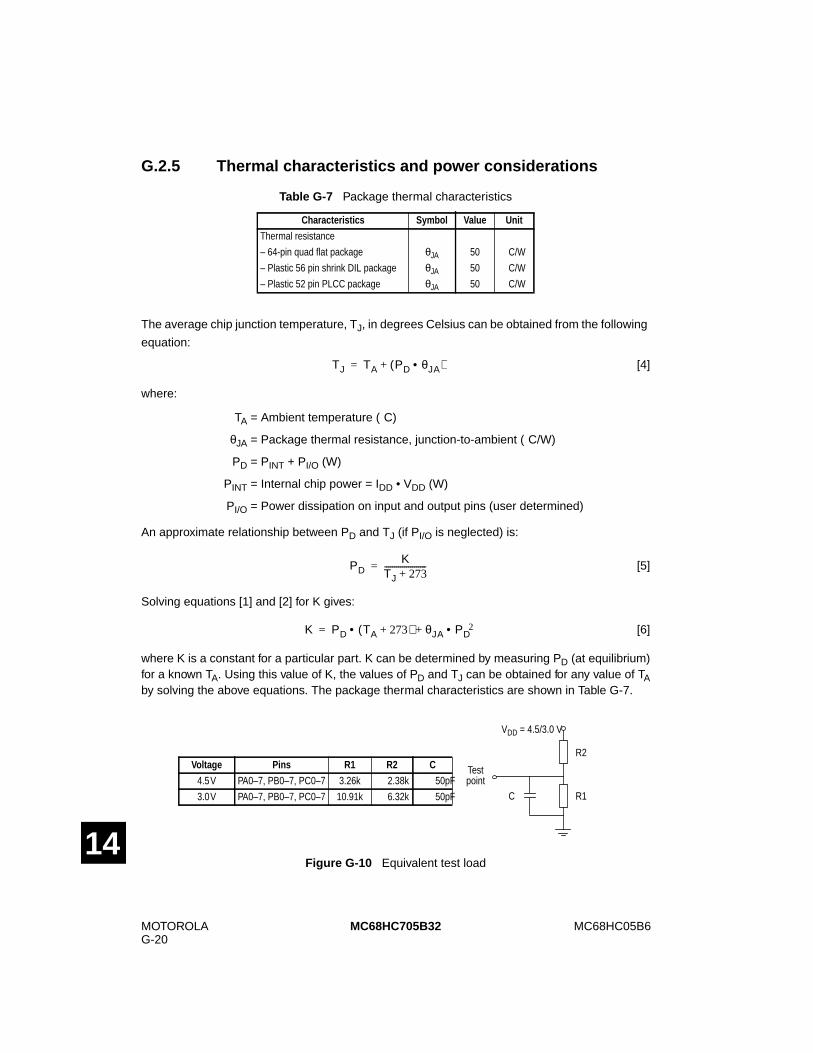
MOTOROLAG-20
MC68HC05B6MC68HC705B32
14
G.2.5 Thermal characteristics and power considerations
The average chip junction temperature, TJ, in degrees Celsius can be obtained from the following
equation:
[4]
where:
TA = Ambient temperature (¡C)
θJA = Package thermal resistance, junction-to-ambient (¡C/W)
PD = PINT + PI/O (W)
PINT = Internal chip power = IDD • VDD (W)
PI/O = Power dissipation on input and output pins (user determined)
An approximate relationship between PD and TJ (if PI/O is neglected) is:
[5]
Solving equations [1] and [2] for K gives:
[6]
where K is a constant for a particular part. K can be determined by measuring PD (at equilibrium)for a known TA. Using this value of K, the values of PD and TJ can be obtained for any value of TAby solving the above equations. The package thermal characteristics are shown in Table G-7.
Table G-7 Package thermal characteristics
Characteristics Symbol Value Unit
Thermal resistance
– 64-pin quad flat package θJA 50 ¡C/W
– Plastic 56 pin shrink DIL package θJA 50 ¡C/W
– Plastic 52 pin PLCC package θJA 50 ¡C/W
Figure G-10 Equivalent test load
TJ TA PD θJA•( )+=
PDK
TJ 273+---------------------=
K PD TA 273+( )• θJA PD2•+=
VDD = 4.5/3.0 V
R2
R1C
Testpoint
Voltage Pins R1 R2 C
4.5V PA0–7, PB0–7, PC0–7 3.26k½ 2.38k½ 50pF
3.0V PA0–7, PB0–7, PC0–7 10.91k½ 6.32k½ 50pF
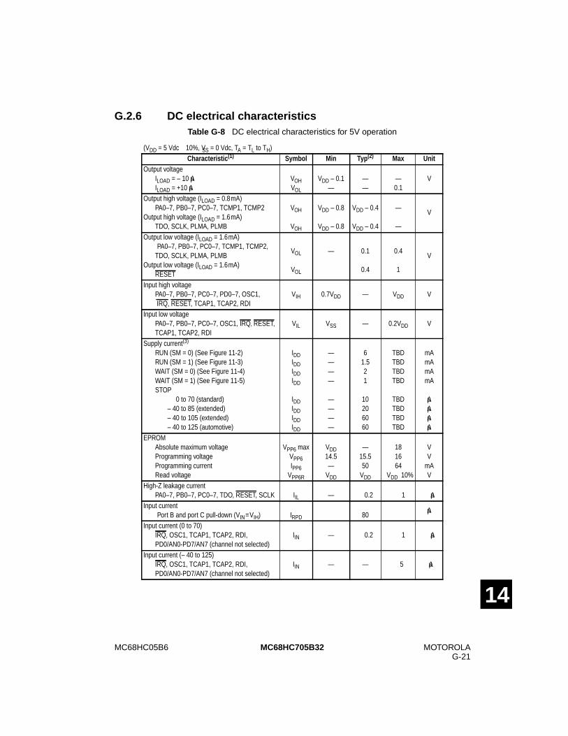
MC68HC05B6 MOTOROLAG-21
MC68HC705B32
14
G.2.6 DC electrical characteristicsTable G-8 DC electrical characteristics for 5V operation
(VDD = 5 Vdc ± 10%, VSS = 0 Vdc, TA = TL to TH)Characteristic (1) Symbol Min Typ (2) Max Unit
Output voltageILOAD = – 10 µAILOAD = +10 µA
VOHVOL
VDD – 0.1—
——
—0.1
V
Output high voltage (ILOAD = 0.8mA)PA0–7, PB0–7, PC0–7, TCMP1, TCMP2
Output high voltage (ILOAD = 1.6mA)TDO, SCLK, PLMA, PLMB
VOH
VOH
VDD – 0.8
VDD – 0.8
VDD – 0.4
VDD – 0.4
—
—
V
Output low voltage (ILOAD = 1.6mA)PA0–7, PB0–7, PC0–7, TCMP1, TCMP2,
TDO, SCLK, PLMA, PLMBOutput low voltage (ILOAD = 1.6mA)
RESET
VOL
VOL
— 0.1
0.4
0.4
1
V
Input high voltagePA0–7, PB0–7, PC0–7, PD0–7, OSC1,IRQ, RESET, TCAP1, TCAP2, RDI
VIH 0.7VDD — VDD V
Input low voltagePA0–7, PB0–7, PC0–7, OSC1, IRQ, RESET,TCAP1, TCAP2, RDI
VIL VSS — 0.2VDD V
Supply current(3)
RUN (SM = 0) (See Figure 11-2)RUN (SM = 1) (See Figure 11-3)WAIT (SM = 0) (See Figure 11-4)WAIT (SM = 1) (See Figure 11-5)STOP
0 to 70 (standard)– 40 to 85 (extended)– 40 to 105 (extended)– 40 to 125 (automotive)
IDDIDDIDDIDD
IDDIDDIDDIDD
————
————
61.521
10206060
TBDTBDTBDTBD
TBDTBDTBDTBD
mAmAmAmA
µAµAµAµA
EPROMAbsolute maximum voltageProgramming voltageProgramming currentRead voltage
VPP6 maxVPP6IPP6
VPP6R
VDD14.5—
VDD
—15.550
VDD
181664
VDD±10%
VV
mAV
High-Z leakage currentPA0–7, PB0–7, PC0–7, TDO, RESET, SCLK IIL — ±0.2 ±1 µA
Input currentPort B and port C pull-down (VIN=VIH) IRPD 80
µA
Input current (0 to 70)IRQ, OSC1, TCAP1, TCAP2, RDI,PD0/AN0-PD7/AN7 (channel not selected)
IIN — ±0.2 ±1 µA
Input current (– 40 to 125)IRQ, OSC1, TCAP1, TCAP2, RDI,PD0/AN0-PD7/AN7 (channel not selected)
IIN — — ±5 µA
MOTOROLAG-22
MC68HC05B6MC68HC705B32
14
(1) All IDD measurements taken with suitable decoupling capacitors across the power supply to suppress thetransient switching currents inherent in CMOS designs (see Section 2).
(2) Typical values are at mid point of voltage range and at 25¡C only.
(3) RUN and WAIT IDD: measured using an external square-wave clock source (fOSC = 4.2MHz); all inputs 0.2 Vfrom rail; no DC loads; maximum load on outputs 50pF (20pF on OSC2).STOP /WAIT IDD: all ports configured as inputs; VIL = 0.2 V and VIH = VDD – 0.2 V: STOP IDD measured withOSC1 = VDD.WAIT IDD is affected linearly by the OSC2 capacitance.
CapacitancePorts (as input or output), RESET, TDO, SCLKIRQ, TCAP1, TCAP2, OSC1, RDIPD0/AN0–PD7/AN7 (A/D off)PD0/AN0–PD7/AN7 (A/D on)
COUTCOUTCINCIN
————
——1222
128——
pFpFpFpF
Table G-8 DC electrical characteristics for 5V operation (Continued)
(VDD = 5 Vdc ± 10%, VSS = 0 Vdc, TA = TL to TH)Characteristic (1) Symbol Min Typ (2) Max Unit
MC68HC05B6 MOTOROLAG-23
MC68HC705B32
14
(1) All IDD measurements taken with suitable decoupling capacitors across the power supply to suppress thetransient switching currents inherent in CMOS designs (see Section 2).
(2) Typical values are at mid point of voltage range and at 25¡C only.
(3) RUN and WAIT IDD: measured using an external square-wave clock source (fOSC = 2.1MHz); all inputs 0.2 Vfrom rail; no DC loads; maximum load on outputs 50pF (20pF on OSC2).STOP /WAIT IDD: all ports configured as inputs; VIL = 0.2 V and VIH = VDD – 0.2 V: STOP IDD measured withOSC1 = VDD.WAIT IDD is affected linearly by the OSC2 capacitance.
Table G-9 DC electrical characteristics for 3.3V operation
(VDD = 3.3Vdc ± 10%, VSS = 0Vdc, TA = TL to TH)Characteristic (1) Symbol Min Typ (2) Max Unit
Output voltageILOAD = – 10 µAILOAD = +10 µA
VOHVOL
VDD – 0.1—
——
—0.1
V
Output high voltage (ILOAD = 0.8mA)PA0–7, PB0–7, PC0–7, TCMP1, TCMP2
Output high voltage (ILOAD = 1.6mA)TDO, SCLK, PLMA, PLMB
VOH
VOH
VDD – 0.3
VDD – 0.3
VDD – 0.1
VDD – 0.1
—
—
V
Output low voltage (ILOAD = 1.6mA)PA0–7, PB0–7, PC0–7, TCMP1, TCMP2,
TDO, SCLK, PLMA, PLMBOutput low voltage (ILOAD = 1.6mA)
RESET
VOL
VOL
— 0.1
0.2
0.4
0.6
V
Input high voltagePA0–7, PB0–7, PC0–7, PD0–7, OSC1,IRQ, RESET, TCAP1, TCAP2, RDI
VIH 0.7VDD — VDD V
Input low voltagePA0–7, PB0–7, PC0–7, OSC1, IRQ, RESET,TCAP1, TCAP2, RDI
VIL VSS — 0.2VDD V
Supply current(3)
RUN (SM = 0) (See Figure 11-2)RUN (SM = 1) (See Figure 11-3)WAIT (SM = 0) (See Figure 11-4)WAIT (SM = 1) (See Figure 11-5)STOP
0 to 70 (standard)– 40 to 85 (extended)– 40 to 105 (extended)– 40 to 125 (automotive)
IDDIDDIDDIDD
IDDIDDIDDIDD
————
————
31
1.50.5
10104040
TBDTBDTBDTBD
TBDTBDTBDTBD
mAmAmAmA
µAµAµAµA
High-Z leakage currentPA0–7, PB0–7, PC0–7, TDO, RESET, SCLK IIL — ±0.2 ±1 µA
Input current (0 to 70)IRQ, OSC1, TCAP1, TCAP2, RDI,PD0/AN0-PD7/AN7 (channel not selected)
IIN — ±0.2 ±1 µA
Input current (– 40 to 125)IRQ, OSC1, TCAP1, TCAP2, RDI,PD0/AN0-PD7/AN7 (channel not selected)
IIN — — ±5 µA
CapacitancePorts (as input or output), RESET, TDO, SCLKIRQ, TCAP1, TCAP2, OSC1, RDIPD0/AN0–PD7/AN7 (A/D off)PD0/AN0–PD7/AN7 (A/D on)
COUTCOUTCINCIN
————
——1222
128——
pFpFpFpF
MOTOROLAG-24
MC68HC05B6MC68HC705B32
14
G.2.7 A/D converter characteristics
G.2.8 Control timing
(1) Source impedances greater than 10k½ will adversely affect internal charging time during input sampling.
(2) The external system error caused by input leakage current is approximately equal to the product of R source and inputcurrent. Input current to A/D channel will be dependent on external source impedance (see Figure 8-2).
Table G-10 A/D characteristics for 5V operation
(VDD = 5.0 Vdc ± 10%, VSS = 0 Vdc, TA = TL to TH)
Characteristic Parameter Min Max Unit
Resolution Number of bits resolved by the A/D 8 — Bit
Non-linearity Max deviation from the best straight line through the A/Dtransfer characteristics(VRH = VDD and VRL = 0V)
— ± 0.5 LSB
Quantization error Uncertainty due to converter resolution — ± 0.5 LSB
Absolute accuracy Difference between the actual input voltage and thefull-scale equivalent of the binary code output code for allerrors
— ± 1 LSB
Conversion range Analog input voltage range VRL VRH V
VRH Maximum analog reference voltage VRL VDD + 0.1 V
VRL Minimum analog reference voltage VSS – 0.1 VRH V
ÆVR Minimum difference between VRH and VRL 3 — V
Conversion time Total time to perform a single analog to digital conversiona. External clock (OSC1, OSC2)b. Internal RC oscillator
——
3232
tCYCµs
Monotonicity Conversion result never decreases with an increase ininput voltage and has no missing codes
GUARANTEED
Zero input reading Conversion result when VIN = VRL 00 — Hex
Full scale reading Conversion result when VIN = VRH — FF Hex
Sample acquisition time Analog input acquisition samplinga. External clock (OSC1, OSC2)b. Internal RC oscillator(1)
——
1212
tCYCs
Sample/hold capacitance Input capacitance on PD0/AN0–PD7/AN7 — 12 pF
Input leakage(2) Input leakage on A/D pins PD0/AN0–PD7/AN7, VRL, VRH — 1 µA
MC68HC05B6 MOTOROLAG-25
MC68HC705B32
14
(1) Source impedances greater than 10k½ will adversely affect internal charging time during input sampling.
(2) The external system error caused by input leakage current is approximately equal to the product of R source and inputcurrent. Input current to A/D channel will be dependent on external source impedance (see Figure 8-2).
Table G-11 A/D characteristics for 3.3V operation
(VDD = 3.3 Vdc ± 10%, VSS = 0 Vdc, TA = TL to TH)
Characteristic Parameter Min Max Unit
Resolution Number of bits resolved by the A/D 8 — Bit
Non-linearity Max deviation from the best straight line through the A/Dtransfer characteristics(VRH = VDD and VRL = 0V)
— ± 1 LSB
Quantization error Uncertainty due to converter resolution — ± 1 LSB
Absolute accuracy Difference between the actual input voltage and thefull-scale equivalent of the binary code output code for allerrors
— ± 2 LSB
Conversion range Analog input voltage range VRL VRH V
VRH Maximum analog reference voltage VRL VDD + 0.1 V
VRL Minimum analog reference voltage VSS – 0.1 VRH V
ÆVR Minimum difference between VRH and VRL 3 — V
Conversion time Total time to perform a single analog to digital conversionInternal RC oscillator — 32 µs
Monotonicity Conversion result never decreases with an increase ininput voltage and has no missing codes
GUARANTEED
Zero input reading Conversion result when VIN = VRL 00 — Hex
Full scale reading Conversion result when VIN = VRH — FF Hex
Sample acquisition time Analog input acquisition samplingInternal RC oscillator(1) — 12 s
Sample/hold capacitance Input capacitance on PD0/AN0–PD7/AN7 — 12 pF
Input leakage(2) Input leakage on A/D pins PD0/AN0–PD7/AN7, VRL, VRH — 1 µA
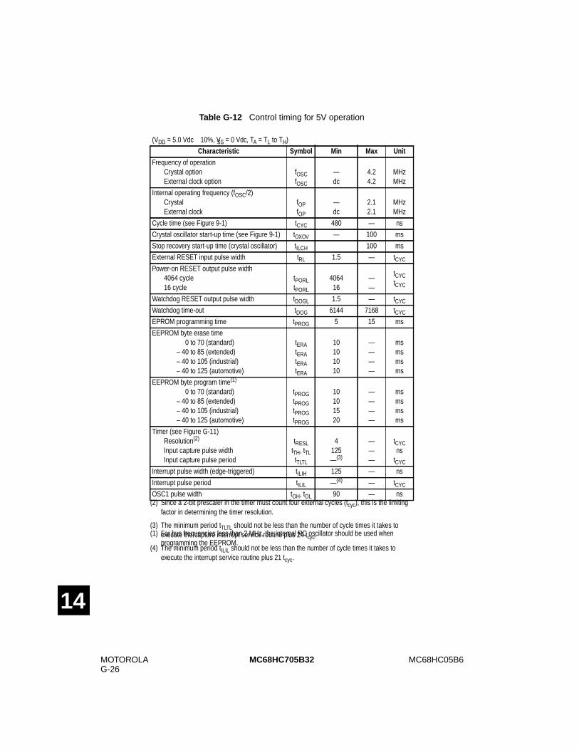
MOTOROLAG-26
MC68HC05B6MC68HC705B32
14
(1) For bus frequencies less than 2 MHz, the internal RC oscillator should be used whenprogramming the EEPROM.
(2) Since a 2-bit prescaler in the timer must count four external cycles (tcyc), this is the limitingfactor in determining the timer resolution.
(3) The minimum period tTLTL should not be less than the number of cycle times it takes toexecute the capture interrupt service routine plus 24 tcyc.
(4) The minimum period tILIL should not be less than the number of cycle times it takes toexecute the interrupt service routine plus 21 tcyc.
Table G-12 Control timing for 5V operation
(VDD = 5.0 Vdc ± 10%, VSS = 0 Vdc, TA = TL to TH)
Characteristic Symbol Min Max Unit
Frequency of operationCrystal optionExternal clock option
fOSCfOSC
—dc
4.24.2
MHzMHz
Internal operating frequency (fOSC/2)CrystalExternal clock
fOPfOP
—dc
2.12.1
MHzMHz
Cycle time (see Figure 9-1) tCYC 480 — ns
Crystal oscillator start-up time (see Figure 9-1) tOXOV — 100 ms
Stop recovery start-up time (crystal oscillator) tILCH 100 ms
External RESET input pulse width tRL 1.5 — tCYC
Power-on RESET output pulse width4064 cycle16 cycle
tPORLtPORL
406416
——
tCYCtCYC
Watchdog RESET output pulse width tDOGL 1.5 — tCYC
Watchdog time-out tDOG 6144 7168 tCYC
EPROM programming time tPROG 5 15 ms
EEPROM byte erase time0 to 70 (standard)
– 40 to 85 (extended)– 40 to 105 (industrial)– 40 to 125 (automotive)
tERAtERAtERAtERA
10101010
————
msmsmsms
EEPROM byte program time(1)
0 to 70 (standard)– 40 to 85 (extended)– 40 to 105 (industrial)– 40 to 125 (automotive)
tPROGtPROGtPROGtPROG
10101520
————
msmsmsms
Timer (see Figure G-11)Resolution(2)
Input capture pulse widthInput capture pulse period
tRESLtTH, tTLtTLTL
4125—(3)
———
tCYCns
tCYC
Interrupt pulse width (edge-triggered) tILIH 125 — ns
Interrupt pulse period tILIL —(4) — tCYC
OSC1 pulse width tOH, tOL 90 — ns
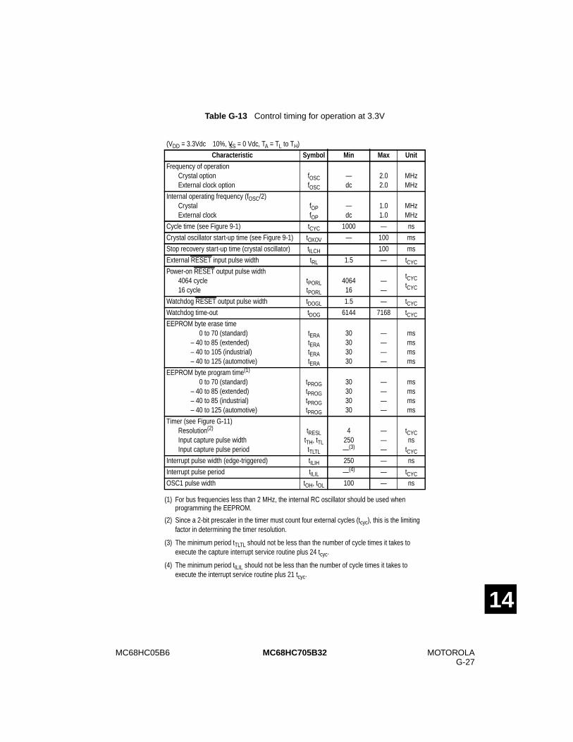
MC68HC05B6 MOTOROLAG-27
MC68HC705B32
14
(1) For bus frequencies less than 2 MHz, the internal RC oscillator should be used whenprogramming the EEPROM.
(2) Since a 2-bit prescaler in the timer must count four external cycles (tcyc), this is the limitingfactor in determining the timer resolution.
(3) The minimum period tTLTL should not be less than the number of cycle times it takes toexecute the capture interrupt service routine plus 24 tcyc.
(4) The minimum period tILIL should not be less than the number of cycle times it takes toexecute the interrupt service routine plus 21 tcyc.
Table G-13 Control timing for operation at 3.3V
(VDD = 3.3Vdc ± 10%, VSS = 0 Vdc, TA = TL to TH)
Characteristic Symbol Min Max Unit
Frequency of operationCrystal optionExternal clock option
fOSCfOSC
—dc
2.02.0
MHzMHz
Internal operating frequency (fOSC/2)CrystalExternal clock
fOPfOP
—dc
1.01.0
MHzMHz
Cycle time (see Figure 9-1) tCYC 1000 — ns
Crystal oscillator start-up time (see Figure 9-1) tOXOV — 100 ms
Stop recovery start-up time (crystal oscillator) tILCH 100 ms
External RESET input pulse width tRL 1.5 — tCYC
Power-on RESET output pulse width4064 cycle16 cycle
tPORLtPORL
406416
——
tCYCtCYC
Watchdog RESET output pulse width tDOGL 1.5 — tCYC
Watchdog time-out tDOG 6144 7168 tCYC
EEPROM byte erase time0 to 70 (standard)
– 40 to 85 (extended)– 40 to 105 (industrial)– 40 to 125 (automotive)
tERAtERAtERAtERA
30303030
————
msmsmsms
EEPROM byte program time(1)
0 to 70 (standard)– 40 to 85 (extended)– 40 to 85 (industrial)– 40 to 125 (automotive)
tPROGtPROGtPROGtPROG
30303030
————
msmsmsms
Timer (see Figure G-11)Resolution(2)
Input capture pulse widthInput capture pulse period
tRESLtTH, tTLtTLTL
4250—(3)
———
tCYCns
tCYC
Interrupt pulse width (edge-triggered) tILIH 250 — ns
Interrupt pulse period tILIL —(4) — tCYC
OSC1 pulse width tOH, tOL 100 — ns
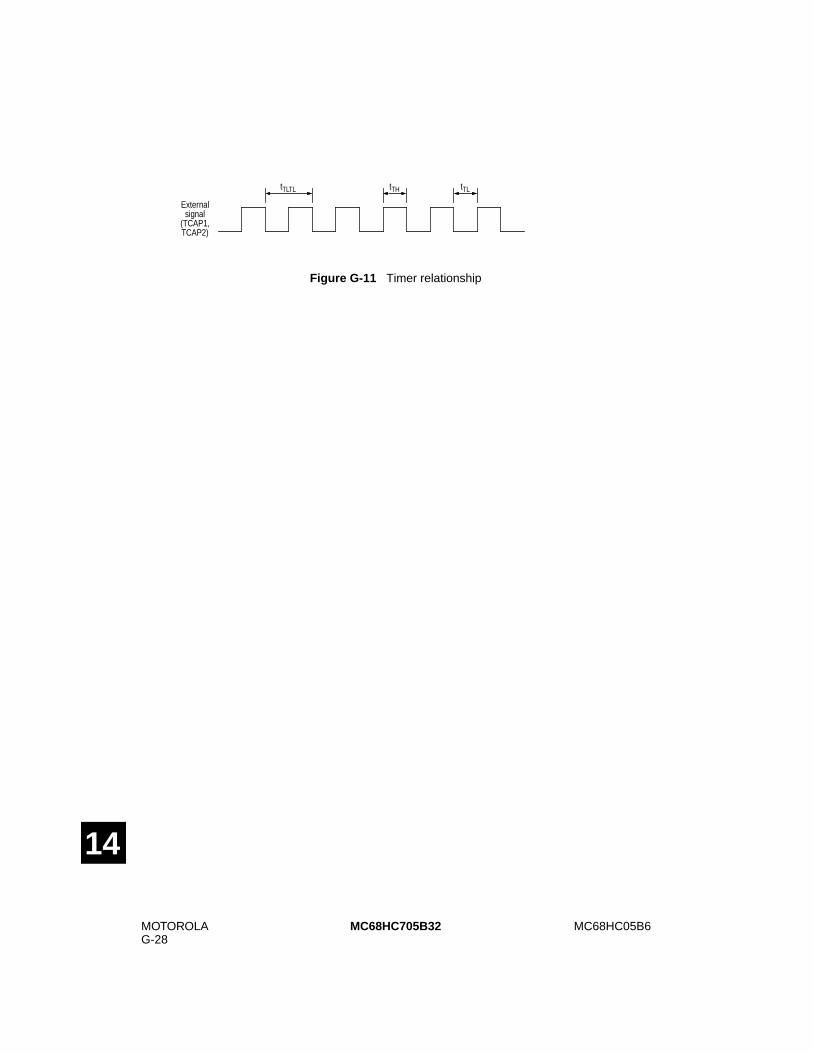
MOTOROLAG-28
MC68HC05B6MC68HC705B32
14
Figure G-11 Timer relationship
Externalsignal
(TCAP1,TCAP2)
tTLTL tTH tTL
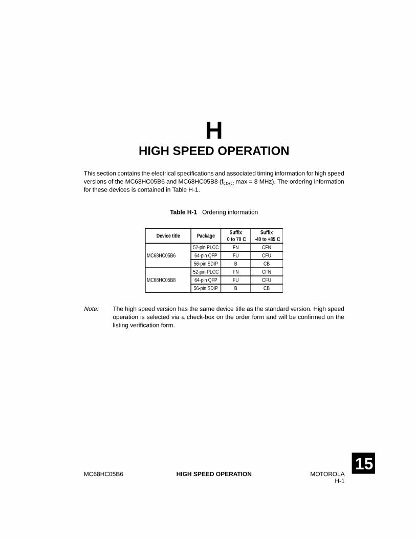
MC68HC05B6 MOTOROLAH-1
HIGH SPEED OPERATION15
HHIGH SPEED OPERATION
This section contains the electrical specifications and associated timing information for high speedversions of the MC68HC05B6 and MC68HC05B8 (fOSC max = 8 MHz). The ordering informationfor these devices is contained in Table H-1.
Note: The high speed version has the same device title as the standard version. High speedoperation is selected via a check-box on the order form and will be confirmed on thelisting verification form.
Table H-1 Ordering information
Device title PackageSuffix
0 to 70¡CSuffix
-40 to +85¡C
MC68HC05B6
52-pin PLCC FN CFN
64-pin QFP FU CFU
56-pin SDIP B CB
MC68HC05B8
52-pin PLCC FN CFN
64-pin QFP FU CFU
56-pin SDIP B CB
MOTOROLAH-2
MC68HC05B6HIGH SPEED OPERATION
15
H.1 DC electrical characteristics
(1) All IDD measurements taken with suitable decoupling capacitors across the power supply to suppress the transientswitching currents inherent in CMOS designs (see Section 2).
(2) Typical values are at mid point of voltage range and at 25¡C only.
(3) RUN and WAIT IDD: measured using an external square-wave clock source (fOSC = 8.0MHz); all inputs 0.2 V fromrail; no DC loads; maximum load on outputs 50pF (20pF on OSC2).STOP /WAIT IDD: all ports configured as inputs; VIL = 0.2 V and VIH = VDD – 0.2 V: STOP IDD measured withOSC1 = VDD.WAIT IDD is affected linearly by the OSC2 capacitance.
Table H-2 DC electrical characteristics for 5V operation
(VDD = 5 Vdc ± 10%, VSS = 0 Vdc, TA = TL to TH)Characteristic (1) Symbol Min Typ (2) Max Unit
Output voltageILOAD = – 10 µAILOAD = +10 µA
VOHVOL
VDD – 0.1—
——
—0.1
V
Output high voltage (ILOAD = 0.8mA)PA0–7, PB0–7, PC0–7, TCMP1, TCMP2
Output high voltage (ILOAD = 1.6mA)TDO, SCLK, PLMA, PLMB
VOH
VOH
VDD – 0.8
VDD – 0.8
———
—
—
V
Output low voltage (ILOAD = 1.6mA)PA0–7, PB0–7, PC0–7, TCMP1, TCMP2,
TDO, SCLK, PLMA, PLMBOutput low voltage (ILOAD = 1.6mA)
RESET
VOL
VOL
———
———
0.4
1
V
Input high voltagePA0–7, PB0–7, PC0–7, PD0–7, OSC1,IRQ, RESET, TCAP1, TCAP2, RDI
VIH 0.7VDD — VDD V
Input low voltagePA0–7, PB0–7, PC0–7, OSC1, IRQ, RESET,TCAP1, TCAP2, RDI
VIL VSS — 0.2VDD V
Supply current(3)
RUN (SM = 0) (See Figure 11-2)RUN (SM = 1) (See Figure 11-3)WAIT (SM = 0) (See Figure 11-4)WAIT (SM = 1) (See Figure 11-5)STOP
0 to 70 (standard)– 40 to 85 (extended)
IDD
————
——
————
——
12342
1020
mAmAmAmA
µAµA
High-Z leakage currentPA0–7, PB0–7, PC0–7, TDO, RESET, SCLK IIL — — ±1 µA
Input current (0 to 70)IRQ, OSC1, TCAP1, TCAP2, RDI,PD0/AN0-PD7/AN7 (channel not selected)
IIN — ——
±5±1
µA
CapacitancePorts (as input or output), RESET, TDO, SCLKIRQ, TCAP1, TCAP2, OSC1, RDIPD0/AN0–PD7/AN7 (A/D off)PD0/AN0–PD7/AN7 (A/D on)
COUTCINCINCIN
————
——1222
128
TBDTBD
pFpFpFpF
MC68HC05B6 MOTOROLAH-3
HIGH SPEED OPERATION15
H.2 A/D converter characteristics
(1) Performance verified down to 2.5V ÆVR, but accuracy is tested and guaranteed at ÆVR = 5V±10%.
(2) Source impedances greater than 10k½ will adversely affect internal charging time during input sampling.
(3) The external system error caused by input leakage current is approximately equal to the product of Rsource and input current. Input current to A/D channel will be dependent on external source impedance(see Figure 8-2).
Table H-3 A/D characteristics for 5V operation
(VDD = 5.0 Vdc ± 10%, VSS = 0 Vdc, TA = TL to TH)
Characteristic Parameter Min Max Unit
Resolution Number of bits resolved by the A/D 8 — Bit
Non-linearityMax deviation from the best straight line throughthe A/D transfer characteristics(VRH = VDD and VRL = 0V)
— ± 0.5 LSB
Quantization error Uncertainty due to converter resolution — ± 0.5 LSB
Absolute accuracyDifference between the actual input voltage andthe full-scale equivalent of the binary codeoutput code for all errors
— ± 1 LSB
Conversion range Analog input voltage range VRL VRH V
VRH Maximum analog reference voltage VRL VDD + 0.1 V
VRL Minimum analog reference voltage VSS – 0.1 VRH V
ÆVR(1) Minimum difference between VRH and VRL 3 — V
Conversion time
Total time to perform a single analog to digitalconversiona. External clock (OSC1, OSC2)b. Internal RC oscillator
——
3232
tCYCµs
MonotonicityConversion result never decreases with anincrease in input voltage and has no missingcodes
GUARANTEED
Zero input reading Conversion result when VIN = VRL 00 — Hex
Full scale reading Conversion result when VIN = VRH — FF Hex
Sample acquisitiontime
Analog input acquisition samplinga. External clock (OSC1, OSC2)b. Internal RC oscillator(2)
——
1212
tCYCs
Sample/holdcapacitance
Input capacitance on PD0/AN0–PD7/AN7 — 12 pF
Input leakage(3) Input leakage on A/D pins PD0/AN0–PD7/AN7VRL, VRH
——
11
µAµA
MOTOROLAH-4
MC68HC05B6HIGH SPEED OPERATION
15
H.3 Control timing for 5V operation
(1) For bus frequencies less than 2 MHz, the internal RC oscillator should be used whenprogramming the EEPROM.
(2) Since a 2-bit prescaler in the timer must count four external cycles (tcyc), this is the limitingfactor in determining the timer resolution.
(3) The minimum period tTLTL should not be less than the number of cycle times it takes toexecute the capture interrupt service routine plus 24 tcyc.
(4) The minimum period tILIL should not be less than the number of cycle times it takes toexecute the interrupt service routine plus 21 tcyc.
(VDD = 5.0 Vdc ± 10%, VSS = 0 Vdc, TA = TL to TH)
Characteristic Symbol Min Max Unit
Frequency of operationCrystal optionExternal clock option
fOSCfOSC
—dc
8.08.0
MHzMHz
Internal operating frequency (fOSC/2)CrystalExternal clock
fOPfOP
—dc
4.04.0
MHzMHz
Cycle time (see Figure 9-1) tCYC 250 — ns
Crystal oscillator start-up time (see Figure 9-1) tOXOV — 100 ms
Stop recovery start-up time (crystal oscillator) tILCH 100 ms
External RESET input pulse width tRL 1.5 — tCYC
Power-on RESET output pulse width4064 cycle16 cycle
tPORLtPORL
406416
——
tCYCtCYC
Watchdog RESET output pulse width tDOGL 1.5 — tCYC
Watchdog time-out tDOG 6144 7168 tCYC
EEPROM byte erase time0 to 70 (standard)
– 40 to 85 (extended)tERAtERA
1010
——
msms
EEPROM byte program time(1)
0 to 70 (standard)– 40 to 85 (extended)
tPROGtPROG
1010
——
msms
Timer (see Figure H-1)Resolution(2)
Input capture pulse widthInput capture pulse period
tRESLtTH, tTLtTLTL
4125—(3)
———
tCYCns
tCYC
Interrupt pulse width (edge-triggered) tILIH 125 — ns
Interrupt pulse period tILIL —(4) — tCYC
OSC1 pulse width tOH, tOL 90 — ns
Figure H-1 Timer relationship
Externalsignal
(TCAP1,TCAP2)
tTLTL tTH tTL
CUSTOMER FEEDBACK QUESTIONNAIRE (MC68HC05B6)Motorola wishes to continue to improve the quality of its documentation. We would welcome your feedback on the publication youhave just received. Having used the document, please complete this card (or a photocopy of it, if you prefer).
1. How would you rate the quality of the document? Check one box in each category.
Excellent Poor Excellent Poor
Organisation Tables
Readability Table of contents
Understandability Index
Accuracy Page size/binding
Illustrations Overall impression
Comments:
2. What is your intended use for this document? If more than one option applies, please rank them (1, 2, 3).
Selection of device for new application Other Please specify:
System design
Training purposes
3. How well does this manual enable you to perform the task(s) outlined in question 2?
Completely Not at all Comments:
4. How easy is it to find the information you are looking for?
Easy Difficult Comments:
5. Is the level of technical detail in the following sections sufficient to allow you to understand how the device functions?
Too little detail Too much detail
Comments:
6. Have you found any errors? If so, please comment:
7. From your point of view, is anything missing from the document? If so, please say what:
– C
ut a
long
this
line
to r
emov
e –
SECTION 1 INTRODUCTION
SECTION 2 MODES OF OPERATION AND PIN DESCRIPTIONS
SECTION 3 MEMORY AND REGISTERS
SECTION 4 INPUT/OUTPUT PORTS
SECTION 5 PROGRAMMABLE TIMER
SECTION 6 SERIAL COMMUNICATIONS INTERFACE
SECTION 7 PULSE LENGTH D/A CONVERTERS
SECTION 8 ANALOG TO DIGITAL CONVERTER
SECTION 9 RESETS AND INTERRUPTS
SECTION 10 CPU CORE AND INSTRUCTION SET
SECTION 11 ELECTRICAL SPECIFICATIONS
SECTION 12 MECHANICAL DATA
SECTION 13 ORDERING INFORMATION
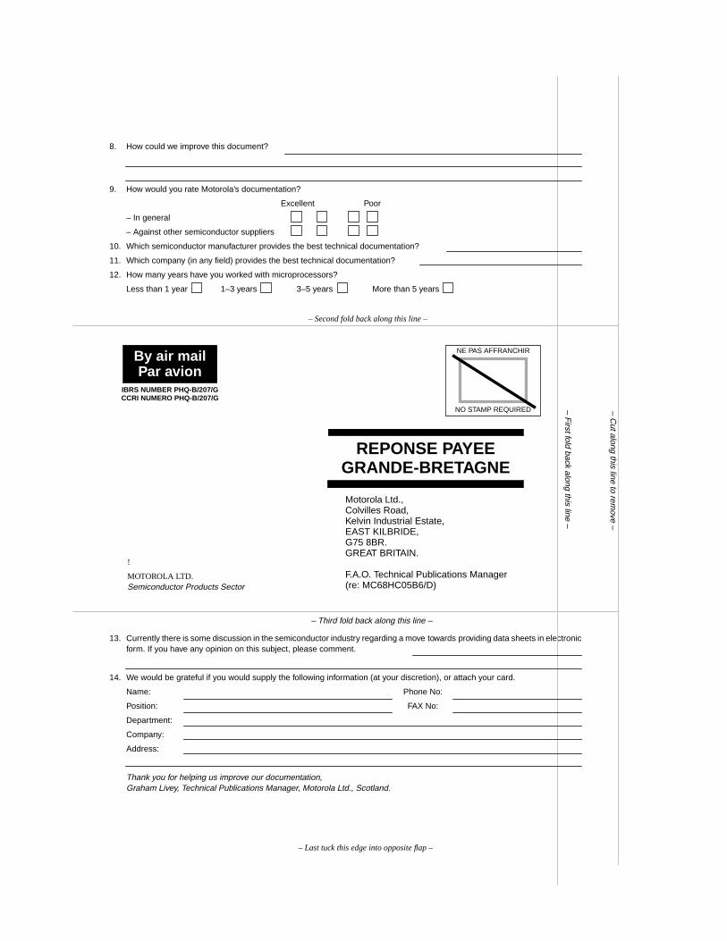
13. Currently there is some discussion in the semiconductor industry regarding a move towards providing data sheets in electronicform. If you have any opinion on this subject, please comment.
14. We would be grateful if you would supply the following information (at your discretion), or attach your card.
Name: Phone No:
Position: FAX No:
Department:
Company:
Address:
Thank you for helping us improve our documentation,Graham Livey, Technical Publications Manager, Motorola Ltd., Scotland.
– Cut along this line to rem
ove –
– Second fold back along this line –
– Third fold back along this line –
– Last tuck this edge into opposite flap –
8. How could we improve this document?
9. How would you rate Motorola’s documentation?
Excellent Poor
– In general
– Against other semiconductor suppliers
10. Which semiconductor manufacturer provides the best technical documentation?
11. Which company (in any field) provides the best technical documentation?
12. How many years have you worked with microprocessors?
Less than 1 year 1–3 years 3–5 years More than 5 years
By air mailPar avion
NE PAS AFFRANCHIR
IBRS NUMBER PHQ-B/207/GCCRI NUMERO PHQ-B/207/G
REPONSE PAYEEGRANDE-BRETAGNE
Motorola Ltd.,Colvilles Road,Kelvin Industrial Estate,EAST KILBRIDE,G75 8BR.GREAT BRITAIN.
F.A.O. Technical Publications Manager(re: MC68HC05B6/D)
NO STAMP REQUIRED – First fold back along this line –
!
MOTOROLA LTD.Semiconductor Products Sector

1
2
3
4
5
6
7
8
9
10
11
12
13
14
15
INTRODUCTION
MODES OF OPERATION AND PIN DESCRIPTIONS
MEMORY AND REGISTERS
INPUT/OUTPUT PORTS
PROGRAMMABLE TIMER
SERIAL COMMUNICATIONS INTERFACE
PULSE LENGTH D/A CONVERTERS
ANALOG TO DIGITAL CONVERTER
RESETS AND INTERRUPTS
CPU CORE AND INSTRUCTION SET
ELECTRICAL SPECIFICATIONS
MECHANICAL DATA
ORDERING INFORMATION
APPENDICES
HIGH SPEED OPERATION
1
2
3
4
5
6
7
8
9
10
11
12
13
14
15
INTRODUCTION
MODES OF OPERATION AND PIN DESCRIPTIONS
MEMORY AND REGISTERS
INPUT/OUTPUT PORTS
PROGRAMMABLE TIMER
SERIAL COMMUNICATIONS INTERFACE
PULSE LENGTH D/A CONVERTERS
ANALOG TO DIGITAL CONVERTER
RESETS AND INTERRUPTS
CPU CORE AND INSTRUCTION SET
ELECTRICAL SPECIFICATIONS
MECHANICAL DATA
ORDERING INFORMATION
APPENDICES
HIGH SPEED OPERATION

2
1
3
4
5
6
7
8
9
10
11
12
13
14
15
2
1
3
4
5
6
7
8
9
10
11
12
13
14
15
Literature Distribution Centres:EUROPE: Motorola Ltd., European Literature Centre, 88 Tanners Drive, Blakelands,
Milton Keynes, MK14 5BP, England.ASIA PACIFIC: Motorola Semiconductors (H.K.) Ltd., Silicon Harbour Center, No. 2, Dai King Street,
Tai Po Industrial Estate, Tai Po, N.T., Hong Kong.JAPAN: Nippon Motorola Ltd., 4-32-1, Nishi-Gotanda, Shinagawa-ku, Tokyo 141, Japan.USA: Motorola Literature Distribution, P.O. Box 20912, Phoenix, Arizona 85036.
!MOTOROLAMC68HC05B6/D

![KNIVES - Grasche · H6 CTK ST 35° W L T Easy Line see page(s) A27 L W T α [mm] [mm] [mm] [°] UMG04 SMG02 KCR08 HC05 7.5 12.0 1.5 35 80360013 80330647 9.6 12.0 1.5 35 80358956 80360014](https://img.pdfslide.net/doc/110x75/5e89a5fa0c084b047416fecc/knives-h6-ctk-st-35-w-l-t-easy-line-see-pages-a27-l-w-t-mm-mm-mm.jpg)