Embed Size (px)
Citation preview

MCM-C Multichip Module Manufacturing Guide
Federal Manufacturing & Technologies
R. J. Blazek,
D. R. Kautz, and
J. V. Galichia
KCP-613-6384
Published November 2000
Topical Report
D. R. Kautz, Project Leader
Approved for public release; distribution is unlimited.
Prepared Under Contract Number DE-ACO4-76-DP00613 for the
United States Department of Energy
1 of 57 3/14/01 3:10 PM
Multichip Module-Ceramic file:///I|/fulltext/f00/096/00096766/sub/6384blaz.htm

DISCLAIMER
This report was prepared as an account of work sponsored by an agency of the United StatesGovernment. Neither the United States Government nor any agency thereof, nor any of their employees,nor any of their contractors, subcontractors or their employees, makes any warranty, express or implied,or assumes any legal liability or responsibility for the accuracy, completeness, or any third party's use orthe results of such use of any information, apparatus, product, or process disclosed, or represents that itsuse would not infringe privately owned rights. Reference herein to any specific commercial product,process, or service by trade names, trademark, manufacturer, or otherwise, does not necessarilyconstitute or imply its endorsement, recommendation, or favoring by the United States Government orany agency thereof or its contractors or subcontractors. The views and opinions of authors expressedherein do not necessarily state or reflect those of the United States Government or any agency thereof.
Printed in the United States of America.
This report has been reproduced from the best available copy.
Available to DOE and DOE contractors from the Office of Scientific and Technical Information, P. O. Box 62, Oak Ridge, Tennessee 37831; prices available from (865) 576-8401, FTS 626-8401 Facsimile: (865) 576-5728, E-mail: [email protected]
Available to the public from the National Technical Information Service, U. S. Department ofCommerce, 5285 Port Royal Rd., Springfield, Virginia 22161, (800) 553-6847, Facsimile: (703) 605-6900, E-mail: [email protected]
A prime contractor with the United States
Department of Energy under Contract Number
DE-ACO4-76-DP00613.
Honeywell
Federal Manufacturing & Technologies
P. O. Box 419159
Kansas City, Missouri
64141-6159
KCP-613-6384
Distribution Category UC-706
2 of 57 3/14/01 3:10 PM
Multichip Module-Ceramic file:///I|/fulltext/f00/096/00096766/sub/6384blaz.htm

Approved for public release; distribution is unlimited.
MCM-C MULTICHIP MODULE MANUFACTURING GUIDE
R. J. Blazek,
D. R. Kautz, and
J. V. Galichia
Published November 2000
Topical Report
D. R. Kautz, Project Leader
Project Team:
R. J. Blazek
J. V. Galichia
©Copyright Honeywell 2000
Contents
Section
Abstract
Summary
Discussion
Scope and Purpose
Activity
Introduction
Reference
Appendices
3 of 57 3/14/01 3:10 PM
Multichip Module-Ceramic file:///I|/fulltext/f00/096/00096766/sub/6384blaz.htm

A. MCM-C Technology
A1 MCM Process Flow
A2 Manufacturing Customer Checklist
A3 Product Definition Checklist
A4 Material Properties
B. LTCC Network Dimensions
B1 LTCC Cross Section
B2 High-Yield Layout
B3 High-Density Layout
B4 Chip and Wire and Cavity Layout
B5 Seal Ring, Braze Pad, and Lid Definition
B6 Thick Film Resistor Layout
B7 Surface Mount Layout
C. MCM-C Examples
D. MCM Reference. Design Specifications for Manufacturability of MCM-C Multichip Modules 40
Illustration
Figure
1 Example MCM-C Configuration
Abstract
The multichip module-ceramic (MCM-C) microcircuit technology using low-temperature cofiredceramic (LTCC) networks has been applied to electronic systems that require increased performance,
4 of 57 3/14/01 3:10 PM
Multichip Module-Ceramic file:///I|/fulltext/f00/096/00096766/sub/6384blaz.htm

reduced volume, and higher density. This MCM-C guide focuses on the manufacturability issues thatmust be considered for LTCC network fabrication and MCM assembly and the effects that processcapabilities have on the MCM design layout and product yield.
Summary
Honeywell Federal Manufacturing & Technologies (FM&T) provides complete microcircuit capabilitiesfrom design layout through manufacturing and final electrical testing. Manufacturing and testingcapabilities include design layout, electrical and mechanical computer simulation and modeling, circuitanalysis, component analysis, network fabrication, microelectronic assembly, electrical tester design,electrical testing, materials analysis, and environmental evaluation.
This document provides manufacturing guidelines for multichip module-ceramic (MCM-C)microcircuits. Figure 1 illustrates an example MCM-C configuration with the parts and processes that areavailable. The MCM-C technology is used to manufacture microcircuits for electronic systems thatrequire increased performance, reduced volume, and higher density that cannot be achieved by thestandard hybrid microcircuit or printed wiring board technologies. The guidelines focus on themanufacturability issues that must be considered for low-temperature cofired ceramic (LTCC) networkfabrication and MCM assembly and the impact that process capabilities have on the overall MCM designlayout and product yield.
Prerequisites that are necessary to initiate the MCM design layout include electrical, mechanical, andenvironmental requirements. Customer design data can be accepted in many standard electronic fileformats. Other requirements include schedule, quantity, cost, classification, and quality level. Designconsiderations include electrical, network, packaging, and producibility; and deliverables includefinished product, drawings, documentation, and electronic files.
5 of 57 3/14/01 3:10 PM
Multichip Module-Ceramic file:///I|/fulltext/f00/096/00096766/sub/6384blaz.htm

Figure 1. Example MCM-C Configuration
Discussion
Scope and Purpose
The scope of this document involved the development of design layout guidelines for LTCC MCMs thatare used for electronic systems. These MCMs typically consist of multilayered cofired thick filmnetworks with chip and wire and/or surface mount assembled components. The purpose of this documentwas to update an existing 73-page document1 and replace it with a simplified, more effective MCM-Cmanufacturing guide in both written and electronic website versions.
Activity
Introduction
This manufacturing guide includes four appendices that provide information about the MCM-Ctechnology, illustrate design layout requirements for LTCC networks, show actual MCM-C assemblies,and provide a reference with MCM-C guidance. Appendix A involves the MCM-C technology andconsists of four sections. Appendix A1 provides an MCM process flow chart that shows the overallrequirements from design layout through manufacturing to final electrical testing. Appendix A2 providesa manufacturing checklist for the customer that summarizes the specific details that should be consideredfor LTCC network design layout. Appendix A3 is a product definition checklist for creating drawingswith material, network fabrication, assembly, component, and electrical testing information. AppendixA4 provides material properties for metals, alloys, substrates, adhesives, semiconductors, solders, andpastes.
Appendix B involves LTCC network dimensions and consists of seven sections. Appendix B1 shows across-section of a typical LTCC network with items identified on the various layers. Appendix B2provides LTCC network dimensions for high-yield layouts. Appendix B3 provides LTCC networkdimensions for high-density layouts. Appendix B4 illustrates LTCC network requirements for chip andwire interconnections and LTCC cavities. Appendix B5 shows requirements for seal rings and LTCCnetwork braze pads and defines dimensions for lids and solder preforms. Appendix B6 identifies thickfilm resistor requirements. Appendix B7 provides LTCC network dimensions for surface mountassembly.
Appendix C provides four actual examples of MCM-C assemblies. Various features are identified foreach example such as the LTCC network layers, chip components, wire interconnections, and nextassembly interconnections. Appendix D provides a reference for MCM-C design layout that is titled"Design Specifications for Manufacturability of MCM-C Multichip Modules."
Reference
1Chris Allen, Roy Blazek, Jay Desch, Jerry Elarton, David Kautz, Dick Markley,
6 of 57 3/14/01 3:10 PM
Multichip Module-Ceramic file:///I|/fulltext/f00/096/00096766/sub/6384blaz.htm
Howard Morgenstern, Ron Stewart, and Larry Warner, Design Specifications for Manufacturability ofMCM-C Multichip Modules, AlliedSignal Federal Manufacturing & Technologies: KCP-613-5430, June1995 (Available from NTIS).
Appendix A
MCM-C Technology
A1. MCM Process Flow
A2. MCM-C Technology: Manufacturing Customer Checklist
PRE-ROUTING TASKS DATE TO BE COMPLETED
DATECOMPLETED
Verification
Schematic vs. draft schematic
7 of 57 3/14/01 3:10 PM
Multichip Module-Ceramic file:///I|/fulltext/f00/096/00096766/sub/6384blaz.htm

Electronic netlist file vs. schematic
Components CAD definition vs. component definitions (library)
Components availability
Electrical / Thermal
Controlled impedance conductor lines
Propagation delay
High current conductor lines
Isolation, shielding and cross talk
Thermal management
Die backside metallization and potential
Printed Resistors
Verify each resistor value
Power dissipation considered for each resistor
Low resistance paths to low value resistors
Probe pads for resistor trimming
Place all resistors for active trimming on one side of LTCC
Provide opening in all resistor loops
Design Definition
Electrical interface
Mechanical interface
LTCC layers (number, planes and XY runs)
LTCC cavity (features and components)
Manufacturability
Network considerations reviewed with engineer
MCM package considerations reviewed with engineer
Testability
8 of 57 3/14/01 3:10 PM
Multichip Module-Ceramic file:///I|/fulltext/f00/096/00096766/sub/6384blaz.htm
Requirements reviewed with test equipment engineer
Test nodes defined for key signals
POST-ROUTING TASKS DATE TO BE COMPLETED
DATECOMPLETED
Verify CAD conductor routing vs. schematic
Verify conductor lines widths/spacings/vias meet designdefinition
Verify special features
Controlled impedance conductor lines (W)
Propagation delay (L)
High current conductor lines (W)
Thermal management
Verify package marking
Verify alignment marks for automatic equipment
Verify placement of pin one indicator for components andnetworks
Verify seal ring, lid and braze pad are correct for final MCMpackage design
Verify testing
Verify final MCM package design against MCMrequirements
9 of 57 3/14/01 3:10 PM
Multichip Module-Ceramic file:///I|/fulltext/f00/096/00096766/sub/6384blaz.htm

requirements
A3. MCM-C Technology: Product Definition Checklist
REQUIRED INFORMATION DATE TO BECOMPLETED
DATECOMPLETED
MCM Graphic Layout
Components and circuitry on one or both sides of thenetwork
Die attachment requirements
Temperature restrictions
Wire length and loop height restrictions
Wire diameter requirements
Wire layout enlargement
Wire and ribbon requirements
Component/lid clearance
Surface mount soldering flag notes
Solder dispensing flag notes
Epoxy dispensing flag notes
Marking requirements
Static handling flag notes
Active trimming flag notes
MCM Material List
Drawings: AY, CK, AC, SS, 99 specs, material specs
LTCC network
Other networks
10 of 57 3/14/01 3:10 PM
Multichip Module-Ceramic file:///I|/fulltext/f00/096/00096766/sub/6384blaz.htm

Epoxy materials
Eutectic die attach materials
Wire and ribbon materials
Solder materials
MCM lid
Components
MCM Schematic
Electrical schematic for verification and troubleshooting
REQUIRED INFORMATION DATE TO BECOMPLETED
DATECOMPLETED
MCM Electrical Test Specifications
Electrical requirements
Electrical test temperatures
Temperature cycling
Power burn-in
Centrifuge test
Shock and vibration
MCM operating and storage conditions
Network Graphic Layout
Network dimensions
Network cavity dimensions
Network solder screen printing requirements
LTCC tape materials
11 of 57 3/14/01 3:10 PM
Multichip Module-Ceramic file:///I|/fulltext/f00/096/00096766/sub/6384blaz.htm

Alignment marks for automated wire bonding, wire pulltesting, component pick-and-place, solder and epoxydispensing
Seal frame solder attachment materials
Pin and lead solder attachment material
Network Material List
DD (Design Definition)
Substrate materials
Thick film paste - chip and wire
Thick film paste - surface mount
Thin film materials
Thick film paste - seal frame
Thick film paste - pins and leads
Pins, leads, seal rings
Screens and stencils
12 of 57 3/14/01 3:10 PM
Multichip Module-Ceramic file:///I|/fulltext/f00/096/00096766/sub/6384blaz.htm

REQUIRED INFORMATION DATE TO BECOMPLETED
DATECOMPLETED
Component Drawings
Component dimensions - length, width and thickness
Component wire bond pad dimensions and pitch
Component materials (Si, GaAs)
Component topside metallization and passivation
Component backside metallization and potential
Die bond pad layout (vendor map)
Component wire bond pads - gold or aluminum
Component termination materials compatible with surfacemount soldering
Component storage conditions
Component Considerations
Component testing (known good die)
Component visual inspection
Component library for future tests and failure analysis
High-yield components using mature technology
Commercial-grade component requirements
Military-grade component requirements
Part Drawings
Lid dimensions
Lid materials and plating conditions
Lid solder attachment materials
13 of 57 3/14/01 3:10 PM
Multichip Module-Ceramic file:///I|/fulltext/f00/096/00096766/sub/6384blaz.htm

A4. MCM-C Technology: Material Properties
This section is a convenient reference of some key properties of materials used in multichip moduleapplications. It summarizes thermal, electrical, mechanical, and processing information on thesematerials, and the parametric values come from a variety of sources listed at the end of the document.
The section contains seven tables as itemized below.
Table 1 Properties of Pure Metals
Table 2 Properties of Alloys
Table 3 Properties of Substrate Materials
Table 4 Properties of Adhesive Materials
Table 5 Properties of Semiconductor Materials
Table 6 Properties of Solder Materials
Table 7 Properties of Paste Materials
Pure Metals
14 of 57 3/14/01 3:10 PM
Multichip Module-Ceramic file:///I|/fulltext/f00/096/00096766/sub/6384blaz.htm

Silver Copper Gold Aluminum Nickel
Parameter Units Ag Cu Au Al Ni
Manufacturer - - - - - - - - - -
Density @ 25° C g/cm3 10.5[1] 8.92[1] 19.3[1] 2.702[1] 8.90[1]
Thermal Conductivity @100° C
W/m-K 427[1] 398[1] 315[1] 237[1] 89.9[1]
Thermal Expansion @ 0°-200° C
ppm/° C 19[1] 16.6[1] 14.2[1] 25[1] 13[1]
Specific Heat J/g-K 0.234[1] 0.385[1] 0.129[1] 0.900[1] 0.444[1]
Young's Modulus GPa 82.7[5] 129.8[5] 78.5[5] 70.6[5] 199.5[5]
Electrical Resistivity @20° C
W -cm 1.59µ [1] 1.67µ [1] 2.35µ [1] 2.65µ [1] 6.84µ[1]
Process Info - MeltingTemperature
° C 962[1] 1083[1] 1064[1] 660[1] 1453[1]
Table 1 Properties of Pure Metals
Alloys
15 of 57 3/14/01 3:10 PM
Multichip Module-Ceramic file:///I|/fulltext/f00/096/00096766/sub/6384blaz.htm

CMSHA-40
Cu-Mo-Cu Invar
Parameter Units Al60/Si40 Mo74/Cu26 Fe64/Ni36
Manufacturer Sumitomo AMAX, Inc. INCO
Density @ 25° C g/cm3 2.53[9] 9.9[10] 8.1[20]
Thermal Conductivity @100° C
W/m-K 138[9] 195[10] 11[20]
Thermal Expansion @ 0°-200° C
ppm/°C
13.5[9] 5.66[10] 1.7-2.0[5]
Specific Heat J/g-K 0.879[9] 0.295[10] 0.515[20]
Young's Modulus GPa 101[9] 228[10] 140-150[5]
Electrical Resistivity @20° C
W -cm 8.35µ [9] 3.5µ [10] 75-85µ [5]
Process Info - MeltingTemperature
° C 2575-2675[25]
Kovar Thermkon76
Parameter Units Fe54/Ni29/Co17 W80/Cu20
Manufacturer Stupakoff Labs CMW, Inc.
Density @ 25° C g/cm3 8.36-8.50[5] 15.56[11]
Thermal Conductivity @100° C
W/m-K 17.1[25] 180[11]
Thermal Expansion @ 0°-200° C
ppm/°C
4.81[5] 7.6[11]
Specific Heat J/g-K
Young's Modulus GPa 14.1[5] 240[11]
Electrical Resistivity @20° C
W -cm 48.9µ [5] 4.21µ [11]
Process Info - MeltingTemperature
° C 1450[25]
16 of 57 3/14/01 3:10 PM
Multichip Module-Ceramic file:///I|/fulltext/f00/096/00096766/sub/6384blaz.htm

Table 2 Properties of Alloys
Substrate Materials
NaturalDiamond Type IIa
CVDDiamond
PolycrystallineDiamond
Parameter Units C C C
Manufacturer Crystallume Diamonex
Density @ 25° C g/cm3 3.515[2] 3.5[16] 3.2 to 3.4[15]
Thermal Conductivity @ 100°C
W/m-K 2000[2] 1300[16] >1300[15]
Thermal Expansion @ 0° -200°C
ppm/° C 1.34[2] 2.0[16] 2[15]
Specific Heat J/g-K 0.519[16]
Young's Modulus GPa 900-1000[2] 1050[24]
Flexural Strength MPa 300[3]
Electrical Resistivity @ 20° C W -cm 104 to >1016[2] 1012 to1016[24]
>1011[15]
Rel. Dielectric Constant @freq
5.68 @ 3kHz[2]
5.7[24] 5.7[15]
Dielectric Loss Tangent @freq
x10-3 10[3] 0.5[14] <0.5 @ 15GHz[15]
Process Info - MeltingTemperature Max Useful Temperature
° C500-700[2]
700[15]
17 of 57 3/14/01 3:10 PM
Multichip Module-Ceramic file:///I|/fulltext/f00/096/00096766/sub/6384blaz.htm
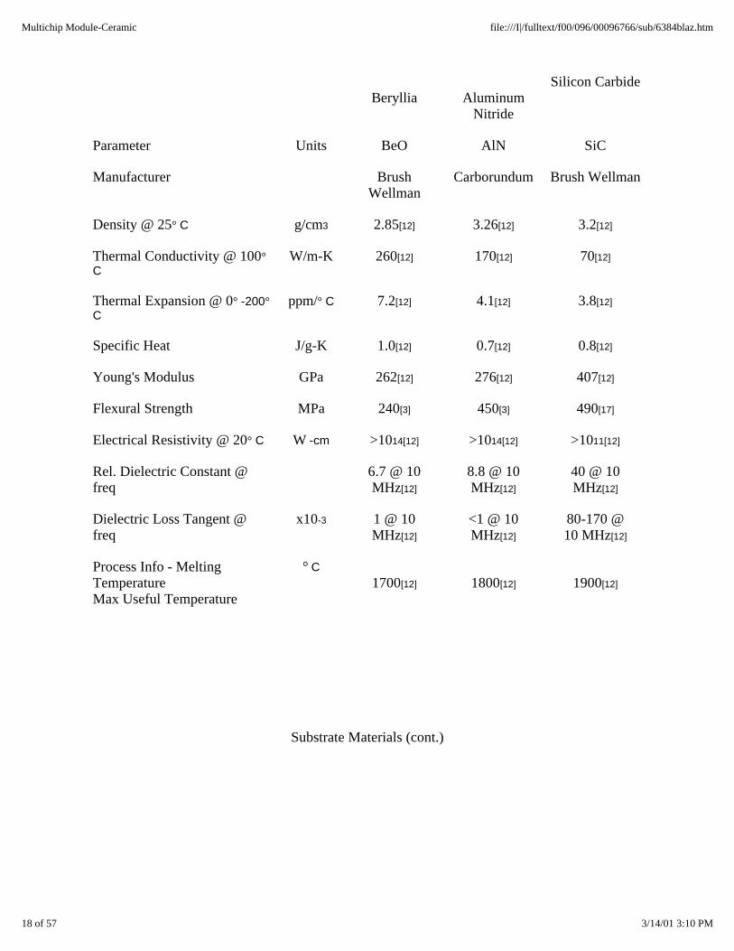
Beryllia Aluminum
Nitride
Silicon Carbide
Parameter Units BeO AlN SiC
Manufacturer BrushWellman
Carborundum Brush Wellman
Density @ 25° C g/cm3 2.85[12] 3.26[12] 3.2[12]
Thermal Conductivity @ 100°C
W/m-K 260[12] 170[12] 70[12]
Thermal Expansion @ 0° -200°C
ppm/° C 7.2[12] 4.1[12] 3.8[12]
Specific Heat J/g-K 1.0[12] 0.7[12] 0.8[12]
Young's Modulus GPa 262[12] 276[12] 407[12]
Flexural Strength MPa 240[3] 450[3] 490[17]
Electrical Resistivity @ 20° C W -cm >1014[12] >1014[12] >1011[12]
Rel. Dielectric Constant @freq
6.7 @ 10MHz[12]
8.8 @ 10MHz[12]
40 @ 10MHz[12]
Dielectric Loss Tangent @freq
x10-3 1 @ 10MHz[12]
<1 @ 10MHz[12]
80-170 @10 MHz[12]
Process Info - MeltingTemperature Max Useful Temperature
° C1700[12] 1800[12] 1900[12]
Substrate Materials (cont.)
18 of 57 3/14/01 3:10 PM
Multichip Module-Ceramic file:///I|/fulltext/f00/096/00096766/sub/6384blaz.htm

Alumina LTCC 901 LTCC951
LTCC 845
Parameter Units 96%Al2O3
Manufacturer Coors Du Pont Du Pont Du Pont
Density @ 25° C g/cm3 3.75[13] 2.89[6] 3.1[6] 2.4[6]
Thermal Conductivity @ 100°C
W/m-K 20[13] 2.0[6] 3.0[6] 2.0[6]
Thermal Expansion @ 0°-200° C
ppm/°C
6.3[13] 7.9[6] 5.7[6] 4.5[6]
Specific Heat J/g-K 0.88[13]
Young's Modulus GPa 303[13]
Flexural Strength MPa 399[13] 229[6] 320[6] 240[6]
Electrical Resistivity @ 20° C W -cm >1014[13]
Rel. Dielectric Constant @freq
9.5 @ 100MHz[13]
7.9 @ 1MHz[6]
7.3 @1 GHz[26]
7.8 @ 10MHz[6]
£ 4.8 @ 5kHz to
5 GHz[6]
Dielectric Loss Tangent @freq
x10-3 0.4 @ 100MHz[13]
3 @ 1 MHz[6]
5 @ 1 GHz[26]
1.5 @ 10MHz[6]
3 @ 5 kHzto 5 GHz[6]
Process Info - MeltingTemperature Max Useful Temperature
° C1500[12] 650[21]
Table 3 Properties of Substrates
Adhesive Materials
19 of 57 3/14/01 3:10 PM
Multichip Module-Ceramic file:///I|/fulltext/f00/096/00096766/sub/6384blaz.htm

Ablebond84-1LMIT Epibond 7002 Epo-Tek
H20E
Parameter Units Silver-filledepoxy
Silver-filledepoxy
Silver-filledepoxy
Manufacturer Abelstik Furane EpoxyTechnology
Density @ 25° C g/cm3 3.99[8] 2.99[18] 2.60[19]
Thermal Conductivity @ 100°C
W/m-K 5.9[8] 1.67[18] 1.59[19]
Thermal Expansion @ 0° -200°C
ppm/°C
52[8] 50[18]
Specific Heat J/g-K
Die Shear Strength @ 25° C MPa 34.5[8] 11.9[18]
Lap Shear Strength @ 25° C MPa 11.0[8] 13.8[18] 10.3[19]
Electrical Resistivity @ 20° C W -cm 70µ [8] 200µ [18] 100-400µ[19]
Process Info - CuringTemperature Glass Transition Temperature
° C 150[8]
103[8]
165[18]
145[18]
50-175[19] 50-60[19]
20 of 57 3/14/01 3:10 PM
Multichip Module-Ceramic file:///I|/fulltext/f00/096/00096766/sub/6384blaz.htm

JM7000
Staystik 101
Staystik 181
Parameter Units Silver-FilledCyanate
Ester
Silver-filledThermoplastic
Silver-filledThermoplastic
Manufacturer Honeywell Cookson Cookson
Density @ 25° C g/cm3
Thermal Conductivity @100° C
W/m-K 1.1[27] 3.0 – 3.5[7] 3.0 – 3.5[7]
Thermal Expansion @ 0°-200° C
ppm/°C
33[27] 40[7] 40[7]
Specific Heat J/g-K 0.46[7] 0.46[7]
Die Shear Strength @ 25° C MPa 17.2[27] 24.1[7] 17.2[7]
Lap Shear Strength @ 25° C MPa
Electrical Resistivity @ 20° C W -cm 2m 500µ [7] 500µ [7]
Process Info - CuringTemperature Glass Transition Temperature
° C 150 - 350[27]
>240[27]
300 - 375[7]
>180[7]
160 - 275[7]
>98[7]
Adhesive Materials (cont.)
21 of 57 3/14/01 3:10 PM
Multichip Module-Ceramic file:///I|/fulltext/f00/096/00096766/sub/6384blaz.htm

Stayform 401 Stayform 501 Stayform 581
Parameter Units Thermoplastic Silver-filledThermoplastic
Silver-filledThermoplastic
Manufacturer Cookson Cookson Cookson
Density @ 25° C g/cm3
Thermal Conductivity @100° C
W/m-K 0.25 – 0.30[7] 3.0 – 3.5[7] 3.0 – 3.5[7]
Thermal Expansion @ 0°-200° C
ppm/° C 60[7] 40[7] 50[7]
Specific Heat J/g-K 1.26[7] 0.46[7] 0.46[7]
Die Shear Strength @ 25° C MPa 24.8[7] 24.1[7] 17.2[7]
Lap Shear Strength @ 25° C MPa
Electrical Resistivity @ 20°C
W -cm >109[7] 500µ [7] 500µ [7]
Rel. Dielectric Constant @freq
3.0 @ 50MHz[7]
Dielectric Loss Tangent @freq
x10-3 10 @ 50MHz[7]
Process Info – CuringTemperature Glass TransitionTemperature
° C 225 - 300[7]
>145[7]
300-375[7]
>180[7]
160 -275[7]
>98[7]
Table 4 Properties of Adhesive Material
Semiconductor Materials
22 of 57 3/14/01 3:10 PM
Multichip Module-Ceramic file:///I|/fulltext/f00/096/00096766/sub/6384blaz.htm

Silicon GalliumArsenide
Parameter Units Si GaAs
Manufacturer
Density @ 25° C g/cm3 2.3283[1] 5.316[1]
Thermal Conductivity @ 100° C W/m-K 83.5[1] 46[3]
Thermal Expansion @ 0° -200°C
ppm/° C 3[1] 6[4]
Specific Heat J/g-K 0.707[1] 0.327[1]
Young's Modulus GPa 131[23] 85.5[23]
Flexural Strength MPa
Electrical Resistivity @ 20° C W -cm 230k[5] 108[22]
Rel. Dielectric Constant @ freq 12[3] 12.9 @4-18 GHz[22]
Dielectric Loss Tangent @ freq x10-3
Process Info - MeltingTemperature
° C 1410[1] 1238[1]
Table 5 Properties of Semiconductor Materials
Solder Materials
23 of 57 3/14/01 3:10 PM
Multichip Module-Ceramic file:///I|/fulltext/f00/096/00096766/sub/6384blaz.htm

Tin/Lead Eutectic
Parameter Units Sn63/Pb37 Au80/Sn20
Manufacturer Williams Williams
Density @ 25° C g/cm3 8.40[25] 14.51[25]
Thermal Conductivity @ 100° C W/m-K 51[25] 68.2[25]
Thermal Expansion @ 0° -200° C ppm/° C 25[25] 15.93[25]
Specific Heat J/g-K
Die Shear Strength @ 25° C Mpa
Lap Shear Strength @ 25° C Pa 41.8[28]
Electrical Resistivity @ 25° C W -cm 1.7n[28]
Process Info - LiquidusTemperature
° C 183[25] 280[25]
Table 6 Properties of Solder Materials
Paste Materials
24 of 57 3/14/01 3:10 PM
Multichip Module-Ceramic file:///I|/fulltext/f00/096/00096766/sub/6384blaz.htm

Primary Purpose Metal Type Resistivity(mohms/sq)
NominalThickness(microns)
Primary Use
Fire System
Via Fill Gold 1 Layer
Conductors Gold 5 6 to 9
Via Fill Silver 1 Layer
Conductor Silver 3.3 6 to 9
Via Fill Palladium/Silver 1 layer
Conductor Palladium/Silver 20 6 to 9
External Post-Fire Materials
Conductors Gold 4 8 Gold WireBondable
Conductors Palladium/
Platinum/Gold
80 15 Tin/Lead Solder
Conductors Palladium/Gold 80 15 Lead/IndiumSolder
Conductors Palladium/Silver 20 15 Tin/Lead Solder
Insulator Glass ---- 12 Cross-overDielectric
Table 7 Properties of Paste Materials
MATERIAL PROPERTIES REFERENCES
[1] Wearst, Robert C., Handbook of Chemistry and Physics, CRC Press, 1975.
[2] Chrenko, R. M. and H. M. Strong, "Physical Properties of Diamond," General Electric CompanyReport No. 75CRD089.
[3] Altshuler, Anatoly M. and John L. Sprague, "The Synthesis, Properties and Applications of DiamondCeramic Materials," Electronic Components & Technology Conference, 1991 Proceedings.
25 of 57 3/14/01 3:10 PM
Multichip Module-Ceramic file:///I|/fulltext/f00/096/00096766/sub/6384blaz.htm

[4] Bernstein, Mary, "CVD Diamond: Taking the Heat," Lasers & Optronics, April 1991, pp. 57-64.
[5] Goodfellow Corporation Catalog 1992-93.
[6] Du Pont Green Tape System Data Sheets.
[7] Staystik, Inc. (New Name, Cookson Semiconductor Package Materials), Product Information.
[8] Ablestik Data Sheet.
[9] Sumitomo Electric CMSH A-40 Data Sheet.
[10] AMAX Speciality Metals Corp., Copper-Clad Moly Data Sheet.
[11] CMW, Inc. (Contact Metals Welding), Series 1200 Properties of CMW Metals, Metal Alloys andContact Metals Brochure.
[12] The Carborundum Company, High Thermal Conductivity Ceramics Comparison, Product DataSheet.
[13] Coors Ceramic Company, ADS-96R Product Data Sheet.
[14] Lu, Grant and E. Fredrick Borchelt, "CVD Diamond Boosts Performance of Laser Diodes,"Photonics Spectra, September 1993, pp. 88-92.
[15] Diamonex, Inc. Porduct Data.
[16] Bernstein, Mary, "CVD Diamond Taking the Heat," Lasers & Optics, April 1991, pp. 57-64.
[17] Kyocera, Product Information.
[18] Furane Products Company, Product Data Sheet.
[19] Epoxy Technology Inc., Product Data Sheet.
[20] Metals Handbook, ASM International, 1990.
[21] Private communications with Du Pont.
[22] Williams, Ralph E., Gallium Arsenide Processing Techniques, Artech House, Inc. 1984.
[23] Howes, M.J., Gallium Arsenide, John Wiley & Sons, Ltd., 1985.
[24] Napolitano, L.M., M.R. Daily, E. Meeks, D. Miller, D.P. Norwood, D.W. Peterson, C.A. Reber,J.E. Robles, and W. Worobey, "Development of a Power Electronics Multichip Module on SyntheticDiamond Substrates," ICEMM Proceedings '93, pp. 92-96.
[25] Williams Advanced Materials, Product Information.
[26] Gipprich, John W., Kevin A. Leahy, Angela J. Martin, Edward L. Rich III, and Kevin W. Sparks,
26 of 57 3/14/01 3:10 PM
Multichip Module-Ceramic file:///I|/fulltext/f00/096/00096766/sub/6384blaz.htm

"Microwave Dielectric Constant of a Low Temperature Co-Fired Ceramic," Proceedings of the 41stElectronic Components & Technology Conference, May, 1991, pp. 20-25.
[27] Honeywell Electronic Materials, Product Data Sheet.
[28] Electronic Materials and Processes Handbook, 1994.
Appendix B
LTCC Network Dimensions
B1. LTCC Cross Section
Low Temperture Cofired Ceramic (LTCC) Networks
Thick film printed conductors and resistors
27 of 57 3/14/01 3:10 PM
Multichip Module-Ceramic file:///I|/fulltext/f00/096/00096766/sub/6384blaz.htm

Multiple conductor planes stacked on each other and interconnected by electrical blind and buried viasand microvias
Hermetic multiple cavities for integrated circuits
Exterior populated with surface mount components
Several varieties of interconnections for next assembly interface
These networks combine all three hybrid technologies
Thick film processing
Chip and wire assembly
Surface mount attachment
B2. High-Yield Layout
LTCC Network Dimensional and Parametric Information and Constraints for a Typical High-Yield MCM Design
(All dimensions are in mils except where noted. 1 mil = 0.001 inch)
General Information on FM&T Capabilities
Maximum Part Size (fired) 3.70 x 3.70 inches
Post Fired Dimensional Tolerances
Pre-Fired Sizing ± 10%
Post-Fired Sizing ± 2 mils
Maximum Number of Layers 50*
* Designer should minimize the number of layers needed.
Camber (mils/inch) 3 typical
Tape Data
28 of 57 3/14/01 3:10 PM
Multichip Module-Ceramic file:///I|/fulltext/f00/096/00096766/sub/6384blaz.htm

The typical shrinkage for the tape from unfired to fired is 13% in the X and Y directions and 15% in theZ direction. Actual shrinkage is tape lot dependent and is controlled by the design expansion factor.
The tape has three thicknesses in the Z direction which are 4.5 unfired (3.8 fired), 6.5 unfired (5.5 fired),and 10 unfired (8.5 fired).
Vias, Electrical
Via sizes are 7 and 10 mil diameters. These via sizes are placed in the unfired tape.
The minimum recommended via diameters are approximately 1x the unfired tape thickness.
The minimum via spacing to the design fired edge of the network shall be 3x the via diameter.
The minimum via-to-via spacing within the same tape layer shall be 3x the average via diameter.
The minimum via stagger between tape layers shall be 2x the via diameter.
Stacking of vias is acceptable. Via staggering is recommended for reducing surface irregularities due tovia material shrinkage being different from the tape. See wire bond pad section for special viarequirements.
Vias, Thermal
Thermal via sizes are 7, 10, and 20 mil diameters placed in an array. A minimum of one layer of viastagger is recommended for hermeticity. The minimum via-to-via spacing shall be 2x the via diameter.
Conductor Lines, Internal
29 of 57 3/14/01 3:10 PM
Multichip Module-Ceramic file:///I|/fulltext/f00/096/00096766/sub/6384blaz.htm
The minimum line width shall be 8 mils (fired).
The minimum conductor spacing shall be 8 mils (fired).
Conductor lines connecting to a via shall be 2 mils larger (unfired) than the via diameter. A catch padshall be added to support this connection recommendation
.
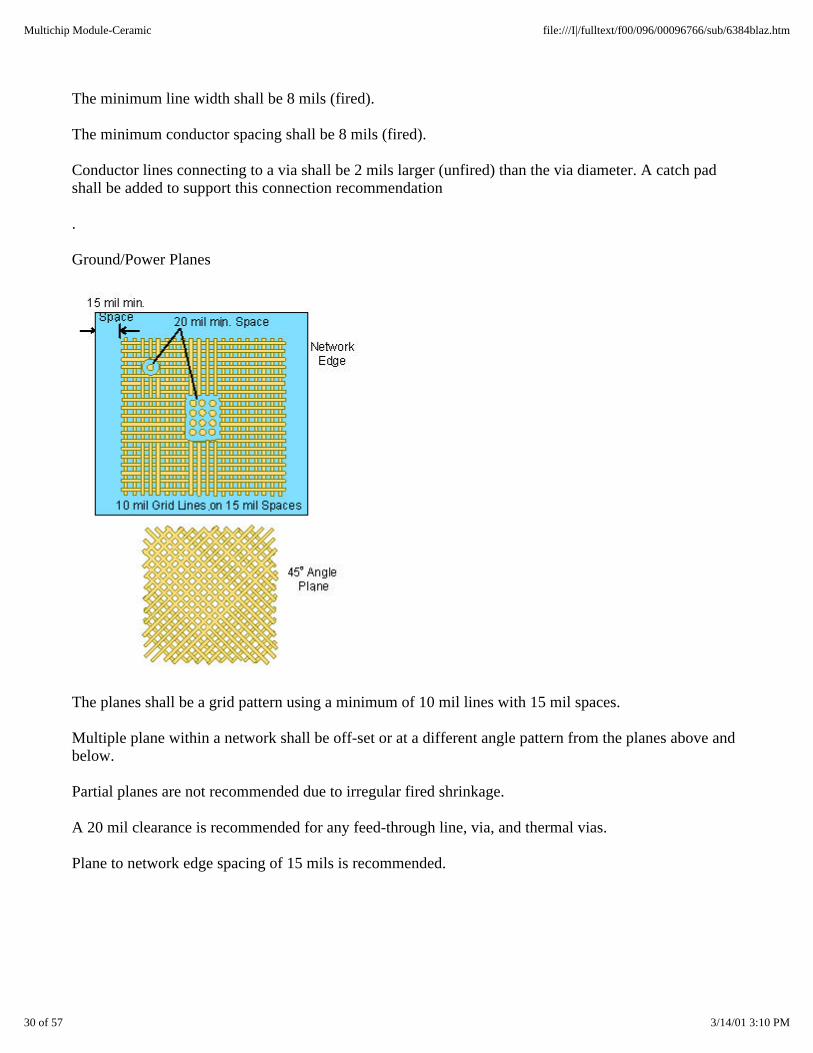
Ground/Power Planes
The planes shall be a grid pattern using a minimum of 10 mil lines with 15 mil spaces.
Multiple plane within a network shall be off-set or at a different angle pattern from the planes above andbelow.
Partial planes are not recommended due to irregular fired shrinkage.
A 20 mil clearance is recommended for any feed-through line, via, and thermal vias.
Plane to network edge spacing of 15 mils is recommended.
30 of 57 3/14/01 3:10 PM
Multichip Module-Ceramic file:///I|/fulltext/f00/096/00096766/sub/6384blaz.htm

B3. High-Density Layout
LTCC Network Dimensional and Parametric Information and Constraints for a Typical High-Density MCM Layout
(All dimensions are in mils except where noted. 1 mil = 0.001 inch)
General Information on FM&T Capabilities
Maximum Part Size (fired) 3.70 x 3.70 inches
Post Fired Dimensional Tolerances
Pre-Fired Sizing ± 10%
Post-Fired Sizing ± 2 mils
Maximum Number of Layers 50*
* Designer should minimize the number of layers needed.
Camber (mils/inch) 3 typical
Tape Data
The typical shrinkage for the tape from unfired to fired is 13% in the X and Y directions and 15% in theZ direction. Actual shrinkage is tape lot dependent and is controlled by the design expansion factor.
The tape has three thicknesses in the Z direction which are 4.5 unfired (3.8 fired), 6.5 unfired (5.5 fired),and 10 unfired (8.5 fired).
Vias, Electrical
Via sizes are 5, 7, and 10 mil diameters. These via sizes are placed in the unfired tape.
The minimum recommended via diameters are approximately 1x the unfired tape thickness.
The minimum via spacing to the design fired edge of the network shall be 3x the via diameter.
The minimum via-to-via spacing within the same tape layer shall be 3x the average via diameter.
31 of 57 3/14/01 3:10 PM
Multichip Module-Ceramic file:///I|/fulltext/f00/096/00096766/sub/6384blaz.htm

The minimum via stagger between tape layers shall be 2x the via diameter.
Stacking of vias is acceptable. Via staggering is recommended for reducing surface irregularities due tovia material shrinkage being different from the tape. See wire bond pad section for special viarequirements.
Vias, Thermal
Thermal via sizes are 7, 10, and 20 mil diameters placed in an array. A minimum of one layer of viastagger is recommended for hermeticity. The minimum via-to-via spacing shall be 2x the via diameter.
Conductor Lines, Internal
The minimum line width shall be 6 mils (fired).
The minimum conductor spacing shall be 6 mils (fired).
Conductor lines connecting to a via shall be 2 mils larger (unfired) than the via diameter. A catch padshall be added to support this connection recommendation. If higher density is required, catch pads maybe eliminated, but yield may be affected.
.
32 of 57 3/14/01 3:10 PM
Multichip Module-Ceramic file:///I|/fulltext/f00/096/00096766/sub/6384blaz.htm

Ground/Power Planes
The planes shall be a grid pattern using a minimum of 10 mil lines with 15 mil spaces.
Multiple plane within a network shall be off-set or at a different angle pattern from the planes above andbelow.
Partial planes are not recommended due to irregular fired shrinkage.
A 15 mil clearance is recommended for any feed-through line, via, and thermal vias.
Plane to network edge spacing of 15 mils is recommended.
B4. Chip and Wire and Cavity Layout
(All dimensions are post-fired, except where noted)
(All dimensions are in mils except where noted. 1 mil = 0.001 inch)
Min/MaxDimension
Typical FigureItem
33 of 57 3/14/01 3:10 PM
Multichip Module-Ceramic file:///I|/fulltext/f00/096/00096766/sub/6384blaz.htm

Network Thickness 40 min (nocavity)
P
LTCC thickness at bottom of cavity 40 min 40 G
Bond wire length [1] 100 max L
Wire bond (width and length) [2] 6 min 10 W & 3
Die mounting pad (width and length beyond die) [3] 5 min 10 1
Die edge distance to edge of wire bond pad. Minimum or2X thickness of die (whichever is greater) ONLY FORWIRE BOND PADS ON THE SAME LAYER AS DIEPAD
20 min 20 2
Wire bond pad via stayout Via dia + 4 2 X via dia. 4
Die bond pad neck down should conform to conductorrequirements
Line widthmin
5
Bond wire angle from die to network wire bond pad 30° max q
Wire bond pad spacing 8 min 10 S & 6
Die to die mounting pad spacing 10 min 10 7
Cavity depth N/A K
First ledge height = Die height +/- 10 for single ledge or
= Die height – 10 for multiple ledges
F
Distance from die edge to cavity wall 10 min 20 E
Wire bond pad length (FOR CAVITY DESIGN), B = C-A 15 min B
Seal ring height (minimum) = Die height (max) – K + M
Where: M – Bond wire loop height + 10 min (20 typical)for wire to lid clearance (see wire information )
20 min H
Cavity edge to seal ring (minimum) = H/Tan φ 20 min 30 J
Cavity ledge length C = (A + D) + (T/Tan φ ) see wireinformation
30 C
Where: Pad pull back 3 min A
Bondable pad length 10 min D
34 of 57 3/14/01 3:10 PM
Multichip Module-Ceramic file:///I|/fulltext/f00/096/00096766/sub/6384blaz.htm

Bond ledge height LTCClayers
T1 & T2
Tool angle 80° Wire bonder f
Wire Information
Wiresize
(mils)
Material Bondtype
Bond padwidth and
length
Wirebondheight
(M)
LTCCcavitywall
clearance
( C )
Max.current
wirelength
>0.040
in.
1.0 Au Ball 10 min 10 min 30 0.65A
1.0 Al Wedge 10 min 10 min 40 0.48A
For other wire and ribbon sizes contact FM&T.
35 of 57 3/14/01 3:10 PM
Multichip Module-Ceramic file:///I|/fulltext/f00/096/00096766/sub/6384blaz.htm

High Density, Fine Pitch
Wire Bond Pad Layout
Cavity and Die Layout Definition Notes
[1] Wire Length. Maximum wire length (bond-to-bond) for high shock or acceleration shall not exceed80 mils.
[2] Wire Bond Pads. Wire bond pads shall be positioned to prevent bonding wires from crossing over
36 of 57 3/14/01 3:10 PM
Multichip Module-Ceramic file:///I|/fulltext/f00/096/00096766/sub/6384blaz.htm

semiconductor die, another bonding wire, or exposed conductor line.
A "1" indicator should be placed next to the number one wire bond pad. This indicator will aid theoperator during the wire bonding process.
Die-to-die wire bonding is not permitted.
Electrical vias should be located away from the wire bonding area to avoid bonding problem.
For multiple wire bonds, increase bond pad 10 mils minimum in direction of bonding.
[3] Die Mounting Pad. Die mounting pads are used for epoxy or eutectic bonding of back-bondedsemiconductor dice (transistors, diodes and integrated circuits) to the substrate metallization.
When attaching semiconductor die it is important that the correct electrical "potential" be connected tothe die mounting pad. That "potential" may be voltage, GND or floating condition.
Die Attachment and Wire Bonder Alignment Marks. A "+" mark shall be placed on opposite cornerswithin the area of the die components and the wire bond pads.
B5. Seal Ring, Braze Pad, and Lid Definition
(All dimensionsare as fired and are in mils. 1 mil = 0.001 inch)
Seal Ring _
Seal ring ID length (SRIDL) = CL + 2A + 2B
Seal ring ID width (SRIDW) = CW + 2A + 2B
Where A = 10 min. (20 typical) and B = 10 min. (typical)
37 of 57 3/14/01 3:10 PM
Multichip Module-Ceramic file:///I|/fulltext/f00/096/00096766/sub/6384blaz.htm

Seal ring OD length (SRODL) = Seal ring ID length + 2 x seal ring width
Seal ring OD width (SRODW) = Seal ring ID width + 2 x seal ring width
where seal ring width is 30 mils for cavity sizes < 1 inch and 50 mils for cavity
sizes > 1 inch
Seal ring OD radius = 30 and ID radius = 20
Note: A large cavity will require a larger seal ring width.
Braze Pad
Braze pad ID length = Seal ring ID length – 2B
Braze pad ID width = Seal ring ID width – 2B
Braze pad OD length = Seal ring OD length +2F
Braze pad OD width = Seal ring OD width + 2F
where F = 10 min. (15 typical)
Braze pad radius should be the same as the seal ring
Lid
Lid length = Seal ring OD length – 2E
Lid width = Seal ring OD width – 2E
where E = 10 min (typical)
Lid radius = same as seal ring
Lid thickness = 10 min. if lid width or length is
less than 0.70 in. and 15 mils min. for larger openings
Lid Solder Preform
Solder ID length = Seal ring ID length + 2C
Solder ID width = Seal ring ID width + 2C
where C = 5 min. (typical)
Solder OD length = Lid OD length
38 of 57 3/14/01 3:10 PM
Multichip Module-Ceramic file:///I|/fulltext/f00/096/00096766/sub/6384blaz.htm

Solder OD width = Lid OD width
Solder preform thickness is 3 +/- 0.3 (typical)
B6. Thick Film Resistor Layout
Thick Film Resistor Definition -- External
There are three basic considerations in designing a thick file resistor: 1) the resistance value; 2) thepower dissipation required; and 3) the allowable resistance tolerance. The resistor value is influenced byits length-to-width ratio, and the power dissipation is a function of the resistor area.
All resistors that are to be trimmed to value must have associated probe pads. Other resistors that do notrequire trimming should still have associated probe pads, since such resistors still must be probed tocheck if they are within specified resistance limits.
When the schematic design includes parallel resistors (for example, resistor loops), a break in anassociated network conductor line shall be provided to establish independence among such resistors fortrimming. The break is closed later during assembly by bridging with a bond wire.
Resistor material is available in decade values of sheet resistance and they are: 10Ω / , 100Ω / ,1,000Ω / , 10,000Ω / , 100,000Ω / , and 1MΩ / .
Power dissipation is a function of the resistor area. For high reliability applications and to compensatefor resistor trimming, such resistors shall be designed with a power density rating of 25 W/sq. in.
A formula for calculating the minimum width of a resistor, given the power dissipation required, is asfollows:
________________
Where: W = √ (P x Ps) / (D x R)
R = Resistor value (KΩ )
P = maximum power dissipation in resistor (mW)
D = power density rating of system (W/sq. in.)
Ps = sheet resistance of resistor material (Ω / )
W = minimum resistor width (mil)
Thick film resistors are trimmed to value. The trimming operation can only provide an increase inresistance. All resistors that must be more precise than 35% shall be designed to 70% of their desiredfinal value.
For resistors that require a tolerance of ± 5% to ± 1%, the following design constraints should beobserved:
39 of 57 3/14/01 3:10 PM
Multichip Module-Ceramic file:///I|/fulltext/f00/096/00096766/sub/6384blaz.htm

Minimum dimension is 0.050 in. Minimum resistor value is 50Ω Maximum resistor length-to-width ratios are 5:1 to 1:5; that is, the length can be as much as 5times the width or as small as 1/5 the width.
Caution: Very large and very small resistors may not necessarily abide by the theoretical formula fordetermining resistor values.
Resistance = Published Sheet Resistance x Length
Width
(All dimensions are post-fired and are in mils. 1 mil = 0.001inch)
Min/MaxDimension
Typical Figure
Item
Resistor length 25 min 50 1
Resistor width 25 min 50 2
Resistor to pad overlap 10 min 10 3
Pad beyond resistor width 5 min 10 4
Pad beyond resistor end 5 min 10 5
Probe pad (length and width) 20 min 30 6
Nearest conductor 15 min 15 7
40 of 57 3/14/01 3:10 PM
Multichip Module-Ceramic file:///I|/fulltext/f00/096/00096766/sub/6384blaz.htm

B7. Surface Mount Layout
(All dimensions are post-fired, except where noted)
(All dimensions are in mils except where noted. 1 mil = 0.001 inch)
41 of 57 3/14/01 3:10 PM
Multichip Module-Ceramic file:///I|/fulltext/f00/096/00096766/sub/6384blaz.htm

Min/Max Dimension Typical FigureItem
Chip bond pad [1]
Chip pad width 35 1
Pad beyond chip width (max width) 5 min 10 2
Pad beyond chip end (max length) 5 min 10 3
Chip to pad overlap 12 min 20 4
Chip pad-to-chip pad spacing 10 min 10 5
LCC Mounting pads [2]
Pad width Same as LCC
Pad length beyond LCC package 20 min 20 6
Nearest conductor 10 min 7
Triple PtAu for all solder pads
First PtAu print As defined minus 2 mils (all sides)
Dielectric window Opening is 2 mils overlap on first print (allsides)
Second PtAu print As defined
Third PtAu print As defined
42 of 57 3/14/01 3:10 PM
Multichip Module-Ceramic file:///I|/fulltext/f00/096/00096766/sub/6384blaz.htm

Surface Mount Layout Definition Notes
[1] Component Solder Pads. When circuits are to be assembled using solder techniques, the conductorsthat receive solder shall be triple-printed. This triple printing makes subsequent soldering operations lesscritical and provides for enhanced conductor adhesion.
Components requiring orientation should include a notch, where possible, on one component solder padto aid part installation.
Use nominal component dimensions when designing solder pad geometries. Pad sizes are designed toaccept component variations from nominal.
Components with length greater than or equal to 200 mils should use the typical pad dimensions orlarger.
Both pads should be the same dimensions to minimize the possibility of component misalignment duringthe soldering operations.
Chip resistors and capacitors with a package size less than 0603 will affect product yields.
43 of 57 3/14/01 3:10 PM
Multichip Module-Ceramic file:///I|/fulltext/f00/096/00096766/sub/6384blaz.htm

[2] LCC Mounting Pads. It is important to obtain an accurate representation of the LCC metallizationpattern.
A "pin one" indicator for an LCC on the substrate is typically a longer solder pad. This uniqueness willaid the operator during the assembly process.
SMT Pick and Place Alignment Marks. A "• " mark will be placed on opposite corners within thearea of the SMT components. The "• " is a 30 mil diameter circle
Surface Mount Package Pad Definitions. See IPC Standard SM782 or www.IPC.org for typical padconfigurations.
Appendix C
MCM-C Examples
MCM-C, 2.24 x 2.24 in.; 32-layer LTCC network; 800 MHz clock frequency; 12,103 electrical vias;thermal vias; 11 silicon and GaAs ICs; 637, 1-mil gold wire interconnections; hermetically sealed active
chip components
44 of 57 3/14/01 3:10 PM
Multichip Module-Ceramic file:///I|/fulltext/f00/096/00096766/sub/6384blaz.htm

MCM-C, 2.0 x 2.0 in.; 16-layer LTCC network; electrical and thermal vias; hermetically sealed ASICand other active chip components; AlN TKN chip carrier; passive surface mount components; PGA pinsfor next assembly interface
MCM-C, 0.676 x 0.676 in.; 6-layer, 2-sided LTCC network; 7-mil electrical vias; hermetically sealedactive chip components with 1-mil gold wire interconnections on one side; passive surface mountcomponents on opposite side; J-leaded edge clips for next assembly interface
45 of 57 3/14/01 3:10 PM
Multichip Module-Ceramic file:///I|/fulltext/f00/096/00096766/sub/6384blaz.htm

MCM-C, 0.870 x 0.780 in.; 6-layer, 2-sided LTCC network; 7-mil electrical vias; hermetically sealedactive analog and digital chip components with 1-mil gold wire interconnections on one side; passivesurface mount components on opposite side; J-leaded edge clips for next assembly interface
Appendix D
MCM Reference
Design Specifications for Manufacturability of MCM-C Multichip Modules
Design Specifications for Manufacturability of MCM-C Multichip Modules
Roy Blazek, Jay Desch, David Kautz, and Howard Morgenstern
AlliedSignal Federal Manufacturing & Technologies*
P.O. Box 419159
Kansas City , MO 64141-6159
Phone: 816-997-4901; Fax: 816-997-3297
46 of 57 3/14/01 3:10 PM
Multichip Module-Ceramic file:///I|/fulltext/f00/096/00096766/sub/6384blaz.htm

Email: [email protected]
Abstract
A comprehensive guide for ceramic-based multichip modules (MCMs) [1] has been developed byAlliedSignal Federal Manufacturing & Technologies (FM&T) to provide manufacturability informationfor its customers about how MCM designs can be affected by existing process and equipmentcapabilities. This guide extends beyond a listing of design rules by providing information about designlayout, low-temperature cofired ceramic (LTCC) substrate fabrication, MCM assembly, and electricaltesting. Electrical, mechanical, packaging, environmental, and producibility issues are reviewed.Examples of three MCM designs are shown in the form of packaging cross-sectional views, LTCCsubstrate layer allocations, and overall MCM photographs. The guide has proven to be an effective toolfor enhancing communications between MCM designers and manufacturers and producing a microcircuitthat meets design requirements within the limitations of process capabilities.
Key Words: Multichip module, Multichip module ceramic (MCM-C), LTCC substrate, manufacturability
Introduction
The development of MCMs using LTCC substrates is a continuing effort by AlliedSignal FM&T to meetfuture microelectronic packaging designs. The complexity of these MCMs requires that concurrentengineering methods be used to decrease overall project flowtime. Future electronic systems will requirethe cofired ceramic MCM technology for the higher performance, smaller volume, faster speed, lighterweight, and higher density that cannot be provided by traditional hybrid microcircuit and printed wiringboard technologies.
In order to meet a customer’s electronic system design requirements, a close relationship must bedeveloped between designers and manufacturers so that the microcircuits required for these electronicsystems can be designed, packaged, and tested within the required cycle time, process yield, and costconstraints. Design guides had been developed for earlier hybrid microcircuit (HMC) production, butredesign and rework resulted when designers stretched to incorporate functional characteristics thatexceeded the HMC process equipment and technology limitations.
The developers of the MCM-C technology realized that a more comprehensive design guide was requiredto transform complex MCM designs into producible microcircuits. As a result, the Design Specificationsfor Manufacturability of MCM-C Multichip Modules was created as part of a Total Quality initiative. Sixsigma manufacturing quality levels can be achieved only if six sigma designs are developed by focusingmore attention at the front end of the design-manufacturing cycle.
The Design Specifications for MCM-C Multichip Modules is a 73-page document that includes electrical,mechanical, environmental, testing, packaging design, and MCM producibility requirements andconsiderations for ceramic MCMs. A review of deliverables includes drawings, documentation, andcomputer-automated design (CAD) files. Seven appendices include material properties, CAD checklists,substrate, assembly, and testing effects on design, component procurement, and MCM-C designexamples.
Customer Requirements
47 of 57 3/14/01 3:10 PM
Multichip Module-Ceramic file:///I|/fulltext/f00/096/00096766/sub/6384blaz.htm

The MCM-C development process sequence includes the customer requirements, MCM design, LTCCsubstrate fabrication, MCM assembly, electrical and environmental testing, and delivery. The knowledgeneeded to define a complete MCM package may be provided by the customer, but more likely aconcurrent effort between the MCM design team and the customer will be required to develop all of thenecessary information. The type of ceramic MCM available at AlliedSignal FM&T is a microelectronicassembly composed of standard and custom-designed integrated circuits and surface mount componentsthat are attached to a multilayer, high density, three-dimensional, interconnected substrate. Some of theelectrical, mechanical, environmental, and testing requirements that will be required by the design teamto manufacture this type of MCM include the following:
Electrical requirements
functional block diagram,
schematic, and
electrical interfaces;
interconnect impedances, terminations, loads, and bandwidths.
Mechanical requirements
size of the MCM,
heat transfer, and
mechanical interfaces;
pin or lead geometry and location,
attachment material composition and next assembly processing conditions,
encapsulation materials, and
location of thermal pathways.
Environmental requirements
operational shock and vibration,
thermal,
hermetic,
atmosphere, and
storage and transportation.
Testing requirements
48 of 57 3/14/01 3:10 PM
Multichip Module-Ceramic file:///I|/fulltext/f00/096/00096766/sub/6384blaz.htm

electrical,
temperature,
burn-in, and
shock and vibration.
In addition to MCM performance, other customer requirements include documentation, cost, quantity,schedule, and quality. Since these items are interrelated and invariably require trade-offs, the design teamcan most effectively analyze and communicate such trade-offs by first understanding the customer’spriorities in these areas.
Packaging Design Requirements
The success of an MCM project is directly related to the concurrent efforts between the customer and thedesign team. The design team includes representatives from electrical, LTCC substrate, MCM assembly,drafting, testing, quality, and manufacturing areas. Packaging design requirements include electricaldesign and testing, LTCC substrate fabrication, and MCM assembly. The design team and customer musthave complete knowledge of the capabilities and interactions of all of these areas in order to obtain amanufacturable design. An MCM producibility assessment is performed before the design is committedto manufacturing.
Electrical Design and Testing
The electrical design of the MCM must produce the schematic definition inclusive of all componentsymbols, signal input/output (I/O) definitions, and signal timing relationships or event sequences. Thisdesign cannot be considered complete until some degree of design testing is successfully conducted, suchas the use of simulation and analysis tools and/or actually breadboarding the design and testing forcorrect functionality.
Once the electrical design has been completed, implementation techniques must be identified that ensurethe required electrical performance. Issues to be resolved include power distribution (voltage, current,grounding) and signal integrity (isolation, controlled impedance interconnects, dielectric effects,propagation delay, MCM I/O launch). The product of this effort should be layout and routing rules, apreliminary layer stackup, dielectric tape selection, and a concept for I/O interconnect to the user system.Module electrical testing and troubleshooting should be considered early in the design so that additionaltest points are incorporated.
A thermal analysis is always in order for any MCM design. The basic goal of thermal analysis is tominimize the thermal impedance between the semiconductor die surface (where active, heat-generatingjunctions are located) and the outer surface of the MCM (where the heat transfer to the environment or tothe user system occurs).
Before finalizing the LTCC substrate layout, the design team must verify the electrical and thermalmanagement designs. This verification avoids increased cost and production delays that result frominaccurate definition. Table 1, which appears in the MCM-C manufacturability guide, provides thedesign team with a checklist to support the initial phase of the design.
49 of 57 3/14/01 3:10 PM
Multichip Module-Ceramic file:///I|/fulltext/f00/096/00096766/sub/6384blaz.htm

Table 1. LTCC Substrate Pre-Routing Checklist
Verification
Schematic vs. draft schematic
Electrical netlist file vs. schematic
Components CAD definition vs. componentdefinition
Considerations
Controlled impedance conductor lines
Propagation delay
High current conductor lines
Isolation, shielding and cross talk
Thermal management
Die backside metallization and potential
Printed resistors
Verify each resistor value
Power dissipation for each resistor
Low resistance paths to low value resistors
Probe pads for resistor trimming
Place all resistors for active trimming onone side of substrate
Provide opening in all resistor loops
Design definition
Electrical interface
Mechanical interface
LTCC layers (number, planes and XY runs)
LTCC cavity (features and components)
Manufacturability
50 of 57 3/14/01 3:10 PM
Multichip Module-Ceramic file:///I|/fulltext/f00/096/00096766/sub/6384blaz.htm

Substrate considerations reviewed withengineer
MCM package considerations reviewedwith engineer
Testability
Requirements reviewed with test equipmentengineer
Test nodes defined for key signals
LTCC Substrate Fabrication
The substrate design/layout and assembly are the concluding processes in the MCM design where all ofthe customer requirements, the manufacturing process capabilities, and the remaining design trade-offoptions are merged together to create the final MCM package definition. The process of creating thepackage definition also defines the substrate features due to the nature of the technology. LTCCsubstrates can serve as both the interconnecting network and the module package.
MCM thermal characteristics are often dominated by the substrate characteristics. One factor impactingsubstrate thermal performance is the thickness of the substrate beneath the heat dissipating devices. Byplacing these devices in cavities, substrate thickness can be reduced. An illustration of the cavity layoutis shown in Figure 1. The minimum and typical dimensions of the substrate and cavity are shown inTable 2. All substrate dimensions are post-fired conditions and are in mm except where noted . Thesubstrate cavity parameters include cofired package thickness, LTCC thickness at the bottom of the cavity, cavity depth, ledgeheight, distance from die edge to cavity wall, seal ring height, cavity edge to seal ring, and cavity ledge length.
Figure 1. Cavity Layout Definition
Table 2. LTCC Substrate Cavity Parameters
Minimum
or TypicalDimension
(mm)
Fig.1
Item
Cofired packagethickness
1.52 min P
51 of 57 3/14/01 3:10 PM
Multichip Module-Ceramic file:///I|/fulltext/f00/096/00096766/sub/6384blaz.htm

LTCC thickness atbottom of cavity
1.02 min G
Cavity depth NA K
First ledge height =Die height ± 0.25 for singleledge or Die height -0.25 formultiple ledges
NA F
Distance from die edgeto cavity wall
0.25 min
0.50 typ
E
Wire bond pad length(FOR CAVITYDESIGN). B=C-A
0.38 min B
Seal ring height (min)= Die height (max)-K+M Where:M=Bond wire loopheight + 0.25 (min) forlid clearance
0.50 min H
Bond wire loop heightfor 0.025 Au wire
0.25 typ
Bond wire loop heightfor 0.127 Al wire
0.76 typ
Cavity edge to sealring (minimum) =H/Tanφ
0.50 min
0.76 typ
J
Cavity bond pad ledgelengthC=(A+D)+(T/Tan φ )
0.76 typ C
Bond pad pull back 0.08 min A
Bondable pad length 0.25 min D
Bond ledge height =Number of LTCClayers • layer’s post-firedthickness
NA T
Tool Angle for wirebonder
70° f
52 of 57 3/14/01 3:10 PM
Multichip Module-Ceramic file:///I|/fulltext/f00/096/00096766/sub/6384blaz.htm

The LTCC substrate thicknesses shown in Table 2 were established to ensure that the substrate will haveadequate package strength. The tightest dimensional tolerance on the contour of the substrate can be heldif the substrate is rectangular. Arcs, keyways, and irregular shapes are possible but not with tighttolerances because they are cut before firing. Substrate layer allocation is related to the designedthickness of the part and the electrical functionality assigned to each layer.
Voltages and grounds are distributed to the components by metal planes designed into specified substratelayers, one plane for each voltage and ground. Each plane is typically composed of metal printed on thespecified layer in a cross-hatched pattern. An adequate number of substrate signal layers must be definedso that all of the MCM interconnections can be successfully routed. Signal layers are normally defined asa pair of two conductor layers where one layer is used to route traces primarily in an X direction whilethe traces on the other layer are routed primarily in the Y direction. This orthogonal routing techniquetends to reduce coupling between layers and retain planar external surfaces.
The manufacturability guide provides a recommended width for internal traces. Wider traces are possiblefor unique signal properties, but the designer is advised that traces with lesser widths can reducesubstrate yield. A recommended diameter for internal electrical vias is specified in the guide. Larger viadiameters are possible, but the ratio of the via diameter to tape thickness becomes critical. Smaller viadiameters are possible, but forcing the ink into the smaller via becomes more difficult, and the substrateyield is reduced. Guidance is provided for minimum spacing between electrical vias and for staggeringvias every two layers. Thermal vias are treated separately from electrical vias, and spacing and diameterrequirements are provided.
A six-page appendix in the MCM-C manufacturability guide provides LTCC substrate information andconstraints on design. Information in this appendix includes a conceptual substrate cross-section andlayer allocation; substrate dimensional and parametric information and constraints for a typical dielectrictape, typical paste properties, seal ring, braze pad, and lid definition; and a substrate specificationsummary.
MCM Assembly
A definition is required for each unique component to be used in the MCM design. The componentcharacteristics which are essential for proper MCM design include the length, width, and thicknessdimensions for each component. Information about bond pad dimensions, pitch, and materialcomposition is required for layout and assembly. A die bond pad layout showing the location of all bondpads with meaningful names is required. This information could be in the form of a die photograph or ascaled drawing. Knowledge of the die technology is required to establish appropriate assembly, handling,and testing processes. Die technology includes semiconductor material, logic type, and information ondie passivation.
Die attach techniques dramatically impact the thermal impedance between the semiconductor die and theLTCC substrate. Electrically conductive and nonconductive epoxies and thermoplastic adhesives areused for die attachment to provide MCM rework capability. Information regarding the semiconductor diebackside metallization is required as it impacts die attach options. Knowledge of the semiconductor diebackside potential is required so that the die attach pad may be connected to the proper voltage orallowed to float. As in the case of die attach, passive component attachment techniques and materialselection can be critical to the thermal performance.
53 of 57 3/14/01 3:10 PM
Multichip Module-Ceramic file:///I|/fulltext/f00/096/00096766/sub/6384blaz.htm

Die components should be placed on the substrate to provide adequate room for attachment andconnection. Components should be placed and oriented for the shortest trace interconnect lengths. Theinterconnect length of high-speed signal traces requires particular attention. After each die has beenattached to the substrate, it must be electrically interconnected to the substrate. This interconnect isaccomplished with wires bonded between appropriate die and substrate bond pads. Themanufacturability guide shows specific physical limitations for substrate bond pad size and spacing, wirelengths, current carrying capabilities, and rework procedures.
Surface mount components are usually leadless chip carriers, chip resistors, or chip capacitors.Interconnect traces for these components are typically located on internal layers of the substrate. Thesurface mount pads that are used for attaching these components must be triple-printed to prevent solderleaching. The solders selected for attachment of surface mount components must be compatible with thesubstrate metallization and component termination materials. Solder can be applied to the substrate byscreen printing, preforms, or automated dispensing. Component reflow soldering can be done by usingconvection or infrared belt furnaces or a vapor phase chamber.
Brazing (high-temperature soldering) is used to attach pins or leads and a seal ring to the substrate. Theability to braze a seal ring to the substrate allows a hermetic die cavity to be formed with the addition ofa lid. Pins or leads are typically used for the electrical interface and mechanical support between theMCM and the user system. The dimensions of these parts must be defined. Several constraints andrecommendations on the design of a seal ring, its braze pad, and the companion lid are shown in themanufacturability guide.
A 16-page appendix in the MCM-C manufacturability guide provides assembly information andconstraints on design. Information in this appendix includes an assembly drawing checklist; cavity andcomponent layout definition; surface mount layout definition; substrate pin, lead, and seal ringattachment; die attachment; wire bonding; gold ribbon bonding; sealing and leak testing; and surfacemount assembly. Assembly and rework limitations are shown for each process with descriptions ofmaterials, process times and temperatures, and available equipment.
MCM Producibility
When an MCM design is completed but before it is committed to manufacturing, a final assessment ofthe producibility must be conducted. This assessment is the culmination of an on-going producibilityassessment which should have been occurring throughout the design process.
The producibility of the design can be influenced by the availability and quality of the pieceparts,particularly die components such as Application Specific Integrated Circuits (ASICs). Unlike packagedcomponents, when a die is incorporated into the design, it is not readily replaceable with a functionallyidentical die from another supplier. Even if die quantities are expected to be available, additional dietesting may be required to ensure die quality (known good die) prior to assembly; otherwise, excessivedie replacement rework will be inevitable.
The ability to manufacture an MCM design must not only address the availability of those processes andequipment directly related to the assembly of the MCM but also the processes and equipment required toproduce all parts of the MCM such as the LTCC substrate. While all processes and equipment may beavailable, acceptable producibility must also permit an achievable assembly sequence that provides dieprotection, cleanliness, and decreasing process temperatures with subsequent processing steps.
54 of 57 3/14/01 3:10 PM
Multichip Module-Ceramic file:///I|/fulltext/f00/096/00096766/sub/6384blaz.htm

MCM Examples
The manufacturability guide includes three design examples; this paper will only describe two. Theprocessor module (PM) is shown in Figure 2, which is a 5.08 X 5.08 cm package with 165 PGA pins forelectrical interface. This module performs all the processing and decision-making functions as part of acontroller system. A surface mount read only memory (ROM) provides capability to define the module’stask.
Figure 2. PM with Open Cavity
Figure 3 shows the cross-sectional view of the cavity area of the processor module. Some of the PMfeatures are a two-tiered wire bondout cavity for the large digital ASIC, a sixteen-layer low temperaturecofired ceramic substrate, and a high thermal conducting thick film aluminum nitride diode chipsubcarrier with thermal vias.
Figure 3. PM - Package Cross-Sectional View
Figure 4 shows PM layer allocation. The substrate thickness will be based on the mechanicalrequirements of the substrate and its physical features including those layers which form the die cavity.The electrical functionality of the substrate layers will be assigned based on the number of ground and/orpower planes required and the electrical interconnect density of the signal layers.
55 of 57 3/14/01 3:10 PM
Multichip Module-Ceramic file:///I|/fulltext/f00/096/00096766/sub/6384blaz.htm

Figure 4. PM - Substrate Layer Allocation
The input/output module (IOM) is shown in Figure 5, which is a 5.08 X 5.08 cm package with PGA pinsfor electrical interface. This module performs the input level shifting for eight lines and provides outputdrives.
Figure 5. IOM with Open Cavity
Figure 6 shows the cross-sectional view of the cavity area of the input/output module. Some of thefeatures are an analog ASIC, an eight-layer low temperature cofired ceramic substrate, and a highthermal conducting thin film aluminum nitride FET subcarrier with staggered thermal vias.
Figure 6. IOM - Package Cross-Sectional View
56 of 57 3/14/01 3:10 PM
Multichip Module-Ceramic file:///I|/fulltext/f00/096/00096766/sub/6384blaz.htm

Conclusions
The development of Design Specifications for Manufacturability of MCM-C Multichip Modules resultedwith an effective reference for creating complex ceramic MCMs within the limitations of the LTCCsubstrate fabrication, MCM assembly, and electrical testing capabilities. By improving the customerknowledge of the overall process and technology effects on design, the producibility of the MCM wasincreased before manufacturing was initiated. By involving the customer in the overalldesign-manufacturing process, design changes and rework could be reduced, and packaging and testingyields could be increased. Adherence to the design rules in the manufacturability guide is expected toproduce MCM designs that lead to optimum substrate, assembly, and testing yields and MCMs that canbe delivered on schedule at a reasonable cost. This manfacturability guide is expected to expand as thetechnology and more complex designs evolve, and as new, higher-capability packaging and testequipment develop.
Acknowledgments
The authors wish to express their gratitude to Chris Allen, Jerry Elarton, Dick Markley, Ron Stewart, andLarry Warner who co-authored the comprehensive guide for ceramic-based multichip modules andSandia National Laboratories/New Mexico for their circuit designs.
Reference
[1] Chris Allen, Roy Blazek, Jay Desch, Jerry Elarton, David Kautz, Dick Markley, HowardMorgenstern, Ron Stewart, and Larry Warner, Design Specifications for Manufacturability of MCM-CMultichip Modules, AlliedSignal Federal Manufacturing & Technologies: KCP-613-5430, June 1995(Available from National Technical Information Service, U.S. Department of Commerce, 5285 PortRoyal Rd., Springfield, Virginia 22161).
57 of 57 3/14/01 3:10 PM
Multichip Module-Ceramic file:///I|/fulltext/f00/096/00096766/sub/6384blaz.htm