Embed Size (px)
Citation preview
MCP1623/24Low-Voltage Input Boost Regulator
for PIC® Microcontrollers
Features
• Up to 96% Typical Efficiency
• 425 mA Typical Peak Input Current Limit:
- IOUT > 50 mA @ 1.2V VIN, 3.3V VOUT
- IOUT > 175 mA @ 2.4V VIN, 3.3V VOUT
- IOUT > 175 mA @ 3.3V VIN, 5.0V VOUT
• Low Start-Up Voltage: 0.65V, 3.3V VOUT @ 1 mA (typical)
• Low Operating Input Voltage: 0.35V, typical 3.3VOUT @ 1 mA
• Adjustable Output Voltage Range: 2.0V to 5.5V
• Maximum Input Voltage VOUT < 5.5V
• Automatic PFM/PWM Operation (MCP1624)
• PWM-Only Operation (MCP1623)
• PWM Operation: 500 kHz
• Low Device Quiescent Current: 19 µA, typical PFM Mode
• Internal Synchronous Rectifier
• Internal Compensation
• Inrush Current Limiting and Internal Soft Start
• True Load Disconnect
• Shutdown Current (All States): <1 µA
• Low Noise, Anti-Ringing Control
• Overtemperature Protection
• Available Packages:
- 6-Lead SOT-23
- 8-Lead 2 x 3 DFN
Applications
• One, Two and Three-Cell Alkaline and NiMH/NiCd Low-Power PIC® Microcontroller Applications
General Description
The MCP1623/24 is a compact, high-efficiency,fixed-frequency, synchronous step-up DC-DCconverter. It provides an easy-to-use power supplysolution for PIC® microcontroller applications poweredby either single-cell, two-cell, or three-cell alkaline,NiCd, NiMH, and single-cell Li-Ion or Li-Polymerbatteries.
Low-voltage technology allows the regulator to start upwithout high inrush current or output voltage overshootfrom a low 0.65V input. High efficiency is accomplishedby integrating the low-resistance N-Channel Boostswitch and synchronous P-Channel switch. Allcompensation and protection circuitry are integrated tominimize external components. For standbyapplications, the MCP1624 operates and consumesonly 19 µA while operating at no load.
A “true” Load Disconnect mode provides input to outputisolation while disabled (EN = GND) by removing thenormal boost regulator diode path from input to output.This mode consumes less than 1 µA of input current.
Output voltage is set by a small external resistordivider.
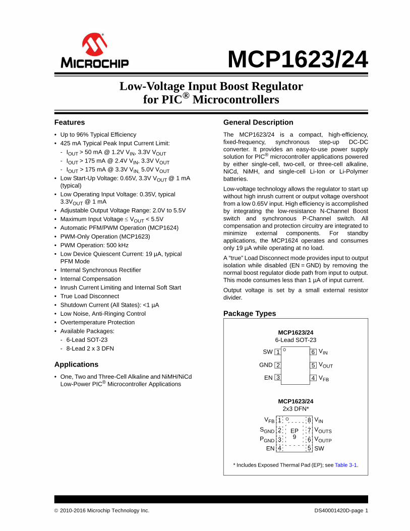
Package Types
3
2
1
4
6 VIN
VFB
SW
GND
EN
5 VOUT
MCP1623/246-Lead SOT-23
MCP1623/242x3 DFN*
PGND
SGND
EN
VOUTS
VOUTP
1
2
3
4
8
7
6
5 SW
VINVFB
EP9
* Includes Exposed Thermal Pad (EP); see Table 3-1.
2010-2016 Microchip Technology Inc. DS40001420D-page 1
MCP1623/24
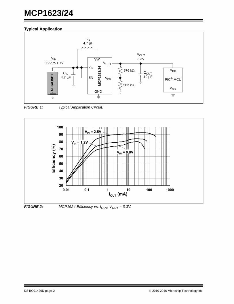
Typical Application
FIGURE 1: Typical Application Circuit.
FIGURE 2: MCP1624 Efficiency vs. IOUT, VOUT = 3.3V.
VIN
GND
VFB
SWVIN 0.9V to 1.7V
VOUT
3.3V
COUT10 µF
CIN4.7 µF
L14.7 µH
VOUT
+
-
976 k
562 k
AL
KA
LIN
E EN PIC® MCU
VDD
VSS
MC
P1
623
/24
20
30
40
50
60
70
80
90
100
0.01 0.1 1 10 100 1000
Eff
icie
nc
y (
%)
IOUT (mA)
VIN = 0.8V
VIN = 1.2V
VIN = 2.5V
DS40001420D-page 2 2010-2016 Microchip Technology Inc.
MCP1623/24
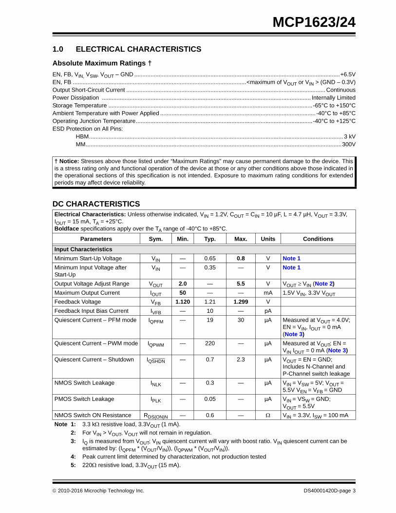
1.0 ELECTRICAL CHARACTERISTICS
Absolute Maximum Ratings †
EN, FB, VIN, VSW, VOUT – GND ...............................................................................................................................+6.5VEN, FB ...........................................................................................................<maximum of VOUT or VIN > (GND – 0.3V)Output Short-Circuit Current ........................................................................................................................... ContinuousPower Dissipation ................................................................................................................................. Internally LimitedStorage Temperature .............................................................................................................................. -65°C to +150°CAmbient Temperature with Power Applied ................................................................................................ -40°C to +85°COperating Junction Temperature............................................................................................................. -40°C to +125°CESD Protection on All Pins:
HBM............................................................................................................................................................. 3 kVMM..............................................................................................................................................................300V
† Notice: Stresses above those listed under “Maximum Ratings” may cause permanent damage to the device. Thisis a stress rating only and functional operation of the device at those or any other conditions above those indicated inthe operational sections of this specification is not intended. Exposure to maximum rating conditions for extendedperiods may affect device reliability.
DC CHARACTERISTICSElectrical Characteristics: Unless otherwise indicated, VIN = 1.2V, COUT = CIN = 10 µF, L = 4.7 µH, VOUT = 3.3V, IOUT = 15 mA, TA = +25°C. Boldface specifications apply over the TA range of -40°C to +85°C.
Parameters Sym. Min. Typ. Max. Units Conditions
Input Characteristics
Minimum Start-Up Voltage VIN — 0.65 0.8 V Note 1
Minimum Input Voltage after Start-Up
VIN — 0.35 — V Note 1
Output Voltage Adjust Range VOUT 2.0 — 5.5 V VOUT VIN (Note 2)
Maximum Output Current IOUT 50 — — mA 1.5V VIN, 3.3V VOUT
Feedback Voltage VFB 1.120 1.21 1.299 V
Feedback Input Bias Current IVFB — 10 — pA
Quiescent Current – PFM mode IQPFM — 19 30 µA Measured at VOUT = 4.0V; EN = VIN, IOUT = 0 mA (Note 3)
Quiescent Current – PWM mode IQPWM — 220 — µA Measured at VOUT; EN = VIN IOUT = 0 mA (Note 3)
Quiescent Current – Shutdown IQSHDN — 0.7 2.3 µA VOUT = EN = GND; Includes N-Channel and P-Channel switch leakage
NMOS Switch Leakage INLK — 0.3 — µA VIN = VSW = 5V; VOUT = 5.5V VEN = VFB = GND
PMOS Switch Leakage IPLK — 0.05 — µA VIN = VSW = GND; VOUT = 5.5V
NMOS Switch ON Resistance RDS(ON)N — 0.6 — VIN = 3.3V, ISW = 100 mA
Note 1: 3.3 k resistive load, 3.3VOUT (1 mA).
2: For VIN > VOUT, VOUT will not remain in regulation.
3: IQ is measured from VOUT; VIN quiescent current will vary with boost ratio. VIN quiescent current can be estimated by: (IQPFM * (VOUT/VIN)), (IQPWM * (VOUT/VIN)).
4: Peak current limit determined by characterization, not production tested
5: 220 resistive load, 3.3VOUT (15 mA).
2010-2016 Microchip Technology Inc. DS40001420D-page 3

MCP1623/24
TEMPERATURE SPECIFICATIONS
PMOS Switch ON Resistance RDS(ON)P — 0.9 — VIN = 3.3V, ISW = 100 mA
NMOS Peak Switch Current Limit
IN(MAX) 300 425 — mA Note 4
VOUT AccuracyVOUT% -7.4 — +7.4 % Includes line and load
regulation; VIN = 1.5V,IOUT = 50 mA
Line Regulation VOUT/ VOUT)/ VIN|
— 0.01 — %/V VIN = 1.5V to 3VIOUT = 25 mA
Load Regulation VOUT/ VOUT|
— 0.01 — % IOUT = 25 mA to 50 mA;VIN = 1.5V
Maximum Duty Cycle DCMAX — 90 — %
Switching Frequency fSW 370 500 630 kHz
EN Input Logic High VIH 90 — — %of VIN IOUT = 1 mA
EN Input Logic Low VIL — — 20 %of VIN IOUT = 1 mA
EN Input Leakage Current IENLK — 0.005 — µA VEN = 5V
Soft Start Time tSS — 750 — µS EN Low-to-High, 90% of VOUT (Note 5)
Thermal Shutdown Die Temperature
TSD — 150 — C
Die Temperature Hysteresis TSDHYS — 10 — C
Electrical Specifications: Unless otherwise indicated, VIN = 1.2V, COUT = CIN = 10 µF, L = 4.7 µH, VOUT = 3.3V, IOUT = 15 mA, TA = +25°C. Boldface specifications apply over the TA range of -40°C to +85°C.
Parameters Sym. Min. Typ. Max. Units Conditions
Temperature Ranges
Operating Junction Temperature Range
TJ -40 — +125 °C Steady state
Storage Temperature Range TA -65 — +150 °C
Maximum Junction Temperature TJ — — +150 °C Transient
Package Thermal Resistance
Thermal Resistance, 6LD-SOT-23 JA — 190.5 — °C/W
Thermal Resistance, 8LD-2x3 DFN JA — 75 — °C/W
DC CHARACTERISTICS (CONTINUED)Electrical Characteristics: Unless otherwise indicated, VIN = 1.2V, COUT = CIN = 10 µF, L = 4.7 µH, VOUT = 3.3V, IOUT = 15 mA, TA = +25°C. Boldface specifications apply over the TA range of -40°C to +85°C.
Parameters Sym. Min. Typ. Max. Units Conditions
Note 1: 3.3 k resistive load, 3.3VOUT (1 mA).
2: For VIN > VOUT, VOUT will not remain in regulation.
3: IQ is measured from VOUT; VIN quiescent current will vary with boost ratio. VIN quiescent current can be estimated by: (IQPFM * (VOUT/VIN)), (IQPWM * (VOUT/VIN)).
4: Peak current limit determined by characterization, not production tested
5: 220 resistive load, 3.3VOUT (15 mA).
DS40001420D-page 4 2010-2016 Microchip Technology Inc.

MCP1623/24
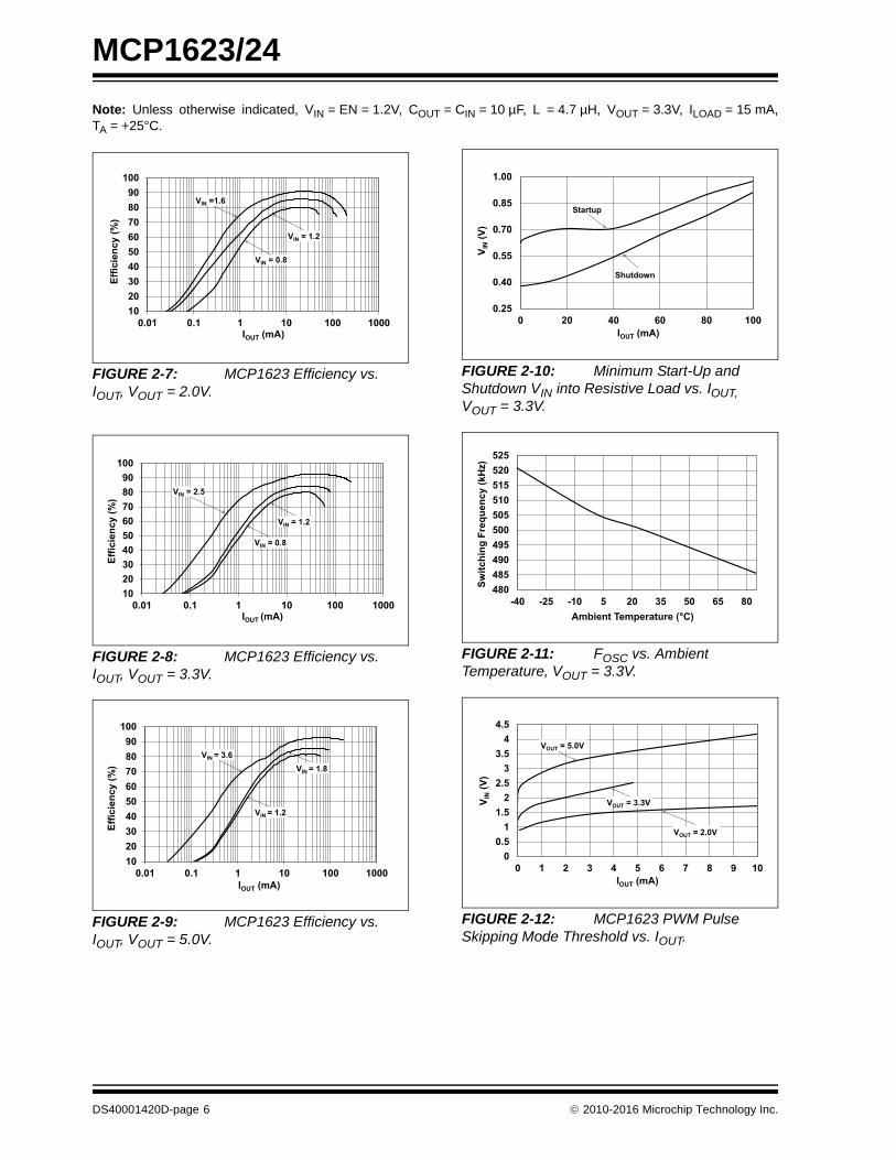
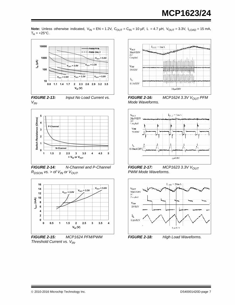
2.0 TYPICAL PERFORMANCE CURVES
Note: Unless otherwise indicated, VIN = EN = 1.2V, COUT = CIN = 10 µF, L = 4.7 µH, VOUT = 3.3V, ILOAD = 15 mA,TA = +25°C.
FIGURE 2-1: MCP1624 VOUT IQ vs. Ambient Temperature in PFM Mode, VIN = 1.2V.
FIGURE 2-2: MCP1623 VOUT IQ vs. Ambient Temperature in PWM Mode, VIN = 1.2V.
FIGURE 2-3: IOUTMAX vs. VOUT.
FIGURE 2-4: MCP1624 Efficiency vs. IOUT, VOUT = 2.0V.
FIGURE 2-5: MCP1624 Efficiency vs. IOUT, VOUT = 3.3V.
FIGURE 2-6: MCP1624 Efficiency vs. IOUT, VOUT = 5.0V.
Note: The graphs and tables provided following this note are a statistical summary based on a limited number ofsamples and are provided for informational purposes only. The performance characteristics listed hereinare not tested or guaranteed. In some graphs or tables, the data presented may be outside the specifiedoperating range (e.g., outside specified power supply range) and therefore outside the warranted range.
10.0
12.5
15.0
17.5
20.0
22.5
25.0
27.5
-40 -25 -10 5 20 35 50 65 80
I Q P
FM
Mo
de
(µ
A)
Ambient Temperature (°C)
VOUT = 2.0V
VOUT = 5.0V
VOUT = 3.3V
150
175
200
225
250
275
300
-40 -25 -10 5 20 35 50 65 80
I Q P
WM
Mo
de
(µ
A)
Ambient Temperature (°C)
VOUT = 3.3V
VOUT = 5.0V
0
100
200
300
400
500
600
0 0.5 1 1.5 2 2.5 3 3.5 4 4.5 5
I OU
T (
mA
)
VIN (V)
VOUT = 3.3V
VOUT = 2.0V VOUT = 5.0V
VIN = 0.8V
VIN = 1.2V
VIN = 1.6V
10
20
30
40
50
60
70
80
90
100
0.01 0.1 1 10 100 1000
Eff
icie
ncy (
%)
IOUT (mA)
VIN = 2.5
VIN = 1.2 VIN = 0.8
10
20
30
40
50
60
70
80
90
100
0.01 0.1 1 10 100 1000
Eff
icie
nc
y (
%)
IOUT (mA)
VIN = 1.2
VIN = 1.8
VIN = 3.6
10
20
30
40
50
60
70
80
90
100
0.01 0.1 1 10 100 1000
Eff
icie
nc
y (
%)
IOUT (mA)
2010-2016 Microchip Technology Inc. DS40001420D-page 5
MCP1623/24
Note: Unless otherwise indicated, VIN = EN = 1.2V, COUT = CIN = 10 µF, L = 4.7 µH, VOUT = 3.3V, ILOAD = 15 mA,TA = +25°C.
FIGURE 2-7: MCP1623 Efficiency vs. IOUT, VOUT = 2.0V.
FIGURE 2-8: MCP1623 Efficiency vs. IOUT, VOUT = 3.3V.
FIGURE 2-9: MCP1623 Efficiency vs. IOUT, VOUT = 5.0V.
FIGURE 2-10: Minimum Start-Up and Shutdown VIN into Resistive Load vs. IOUT, VOUT = 3.3V.
FIGURE 2-11: FOSC vs. Ambient Temperature, VOUT = 3.3V.
FIGURE 2-12: MCP1623 PWM Pulse Skipping Mode Threshold vs. IOUT.
VIN = 0.8
VIN = 1.2
VIN =1.6
10
20
30
40
50
60
70
80
90
100
0.01 0.1 1 10 100 1000
Eff
icie
nc
y (
%)
IOUT (mA)
VIN = 0.8
VIN = 1.2
VIN = 2.5
10
20
30
40
50
60
70
80
90
100
0.01 0.1 1 10 100 1000
Eff
icie
nc
y (
%)
IOUT (mA)
VIN = 1.2
VIN = 1.8 VIN = 3.6
10
20
30
40
50
60
70
80
90
100
0.01 0.1 1 10 100 1000
Eff
icie
nc
y (
%)
IOUT (mA)
0.25
0.40
0.55
0.70
0.85
1.00
0 20 40 60 80 100
VIN
(V
)
IOUT (mA)
Startup
Shutdown
480
485
490
495
500
505
510
515
520
525
-40 -25 -10 5 20 35 50 65 80
Sw
itch
ing
Fre
qu
en
cy (
kH
z)
Ambient Temperature (°C)
0
0.5
1
1.5
2
2.5
3
3.5
4
4.5
0 1 2 3 4 5 6 7 8 9 10
VIN
(V
)
IOUT (mA)
VOUT = 3.3V
VOUT = 5.0V
VOUT = 2.0V
DS40001420D-page 6 2010-2016 Microchip Technology Inc.
MCP1623/24
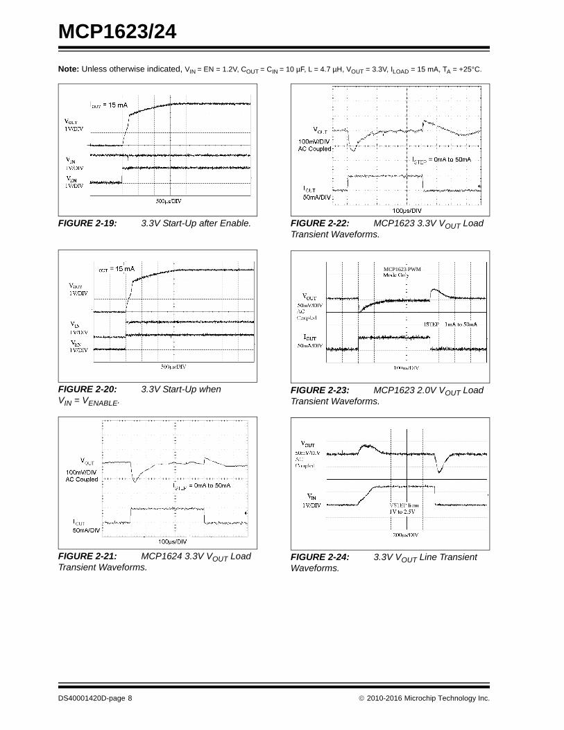
Note: Unless otherwise indicated, VIN = EN = 1.2V, COUT = CIN = 10 µF, L = 4.7 µH, VOUT = 3.3V, ILOAD = 15 mA,TA = +25°C.
FIGURE 2-13: Input No Load Current vs. VIN.
FIGURE 2-14: N-Channel and P-Channel RDSON vs. > of VIN or VOUT.
FIGURE 2-15: MCP1624 PFM/PWM Threshold Current vs. VIN.
FIGURE 2-16: MCP1624 3.3V VOUT PFM Mode Waveforms.
FIGURE 2-17: MCP1623 3.3V VOUT PWM Mode Waveforms.
FIGURE 2-18: High Load Waveforms.
10
100
1000
10000
0.8 1.1 1.4 1.7 2 2.3 2.6 2.9 3.2 3.5
I IN (
µA
)
VIN (V)
VOUT = 3.3V VOUT = 5.0V VOUT = 2.0V
VOUT = 2.0V VOUT = 3.3V
VOUT = 5.0V
PWM/PFM
PWM ONLY
0
1
2
3
4
5
1 1.5 2 2.5 3 3.5 4 4.5 5
Sw
itc
h R
es
ista
nc
e (
Oh
ms
)
> VIN or VOUT
P-Channel
N-Channel
0
2
4
6
8
10
12
14
16
0 0.5 1 1.5 2 2.5 3 3.5 4
I OU
T (
mA
)
VIN (V)
VOUT = 2.0V VOUT = 3.3V
VOUT = 5.0V
2010-2016 Microchip Technology Inc. DS40001420D-page 7
MCP1623/24
Note: Unless otherwise indicated, VIN = EN = 1.2V, COUT = CIN = 10 µF, L = 4.7 µH, VOUT = 3.3V, ILOAD = 15 mA, TA = +25°C.
FIGURE 2-19: 3.3V Start-Up after Enable.
FIGURE 2-20: 3.3V Start-Up when VIN = VENABLE.
FIGURE 2-21: MCP1624 3.3V VOUT Load Transient Waveforms.
FIGURE 2-22: MCP1623 3.3V VOUT Load Transient Waveforms.
FIGURE 2-23: MCP1623 2.0V VOUT Load Transient Waveforms.
FIGURE 2-24: 3.3V VOUT Line Transient Waveforms.
MCP1623 PWM
DS40001420D-page 8 2010-2016 Microchip Technology Inc.

MCP1623/24
3.0 PIN DESCRIPTIONS
The descriptions of the pins are listed in Table 3-1.
TABLE 3-1: PIN FUNCTION TABLE
3.1 Switch Node Pin (SW)
Connects the inductor from the input voltage to the SWpin. The SW pin carries inductor current and can be ashigh as 425 mA peak. The integrated N-Channel switchdrain and integrated P-Channel switch source areinternally connected at the SW node.
3.2 Ground Pin (GND)
The ground or return pin is used for circuit groundconnection. Length of trace from input cap return, outputcap return and GND pin should be made as short aspossible to minimize noise on the GND pin.
3.3 Enable Pin (EN)
The EN pin is a logic-level input used to enable ordisable device switching and lower quiescent currentwhile disabled. A logic high (greater than 90% of VIN)will enable the regulator output. A logic low (less than20% of VIN) will ensure that the regulator is disabled.
3.4 Feedback Voltage Pin (FB)
The FB pin is used to provide output voltage regulationby using a resistor divider. The FB voltage will be 1.21Vtypical with the output voltage in regulation.
3.5 Output Voltage Pin (VOUT)
The output voltage pin connects the integratedP-Channel MOSFET to the output capacitor. The FBvoltage divider is also connected to the VOUT pin forvoltage regulation.
3.6 Power Supply Input Voltage Pin (VIN)
Connects the input voltage source to VIN. The inputsource should be decoupled to GND with a 4.7 µFminimum capacitor.
3.7 Signal Ground Pin (SGND)The signal ground pin is used as a return for theintegrated VREF and error amplifier. In the 2x3 DFNpackage, the SGND and power ground (PGND) pins areconnected externally.
3.8 Power Ground Pin (PGND)The power ground pin is used as a return for thehigh--current N-Channel switch. In the 2x3 DFNpackage, the PGND and signal ground (SGND) pins areconnected externally.
3.9 Output Voltage Sense Pin (VOUTS)
The output voltage sense pin connects the regulatedoutput voltage to the internal bias circuits. In the2x3 DFN package, VOUTS and VOUTP are connectedexternally.
3.10 Output Voltage Power Pin (VOUTP)The output voltage power pin connects the outputvoltage to the switch node. High current flows throughthe integrated P-Channel and out of this pin to theoutput capacitor and output. In the 2x3 DFN package,VOUTS and VOUTP are connected externally.
3.11 Exposed Thermal Pad (EP)There is an internal electrical connection between theExposed Thermal Pad (EP) and the VSS pin; they mustbe connected to the same potential on the PrintedCircuit Board (PCB).
MCP1623/24 Symbol Description
SOT-23 2x3 DFN
1 5 SW Switch Node, Boost Inductor Input Pin
2 — GND Ground Pin
3 4 EN Enable Control Input Pin
4 1 FB Feedback Voltage Pin
5 — VOUT Output Voltage Pin
6 8 VIN Input Voltage Pin
— 2 SGND Signal Ground Pin
— 3 PGND Power Ground Pin
— 7 VOUTS Output Voltage Sense Pin
— 6 VOUTP Output Voltage Power Pin
— 9 EP Exposed Thermal Pad (EP); must be connected to VSS.
2010-2016 Microchip Technology Inc. DS40001420D-page 9

MCP1623/24
NOTES:
DS40001420D-page 10 2010-2016 Microchip Technology Inc.
MCP1623/24
4.0 DETAILED DESCRIPTION
4.1 Device Option Overview
The MCP1623/24 family of devices is capable of lowstart-up voltage and delivers high efficiency over a wideload range for single-cell, two-cell, three-cell alkaline,NiMH, NiCd and single-cell Li-Ion battery inputs. A highlevel of integration lowers total system cost, easesimplementation and reduces board area. The devicesfeature low start-up voltage, adjustable output voltage,PWM/PFM mode operation, low IQ, integratedsynchronous switch, internal compensation, low noiseanti-ringing control, inrush current limit and soft start.There is one feature option for the MCP1623/24 family:PWM/PFM mode or PWM mode only.
4.1.1 PWM/PFM MODE OPTION
The MCP1624 devices use an automatic switchoverfrom PWM to PFM mode for light load conditions tomaximize efficiency over a wide range of output current.During PFM mode, higher peak current is used to pumpthe output up to the threshold limit. While operating inPFM or PWM mode, the P-Channel switch is used as asynchronous rectifier, turning off when the inductorcurrent reaches 0 mA to maximize efficiency. In PFMmode, a comparator is used to terminate switching whenthe output voltage reaches the upper threshold limit.Once switching has terminated, the output voltage willdecay or coast down. During this period, very low IQ isconsumed from the device and input source, whichkeeps power efficiency high at light load. Thedisadvantages of PWM/PFM mode are higher outputripple voltage and variable PFM mode frequency. ThePFM mode frequency is a function of input voltage,output voltage and load. While in PFM mode, the boostconverter pumps the output up at a switching frequencyof 500 kHz.
4.1.2 PWM MODE ONLY OPTION
The MCP1623 devices disable PFM mode switching,and operate only in PWM mode over the entire loadrange. During periods of light load operation, theMCP1623 continues to operate at a constant 500 kHzswitching frequency, keeping the output ripple voltagelower than PFM mode. During PWM-only mode, theMCP1623 P-Channel switch acts as a synchronousrectifier by turning off to prevent reverse current flowfrom the output cap back to the input in order to keepefficiency high. For noise immunity, the N-ChannelMOSFET current sense is blanked for approximately100 ns. With a typical minimum duty cycle of 100 ns,the MCP1623 continues to switch at a constantfrequency under light load conditions. Figure 2-12represents the input voltage versus load current for thepulse-skipping threshold in PWM-only mode. At lighterloads, the MCP1623 device begins to skip pulses.
TABLE 4-1: PART NUMBER SELECTION
Part Number PWM/PFM PWM
MCP1623 X
MCP1624 X
2010-2016 Microchip Technology Inc. DS40001420D-page 11

MCP1623/24
4.2 Functional Description
The MCP1623/24 is a compact, high-efficiency,fixed-frequency, step-up DC-DC converter thatprovides an easy-to-use power supply solution forPIC® microcontroller applications powered by eithersingle-cell, two-cell, or three-cell alkaline, NiCd, orNiMH, and single-cell Li-Ion or Li-Polymer batteries.
Figure 4-1 depicts the functional block diagram of theMCP1623/24.
4.2.1 LOW-VOLTAGE START-UP
The MCP1623/24 is capable of starting from a low inputvoltage. Start-up voltage is typically 0.65V for a 3.3Voutput and 1 mA resistive load.
When enabled, the internal start-up logic turns therectifying P-Channel switch on until the outputcapacitor is charged to a value close to the inputvoltage. The rectifying switch is current limited duringthis time. After charging the output capacitor to theinput voltage, the device starts switching. If the inputvoltage is below 1.6V, the device runs open-loop with afixed duty cycle of 70% until the output reaches 1.6V.
During this time, the boost switch current is limited to50% of its nominal value. Once the output voltagereaches 1.6V, normal closed-loop PWM operation isinitiated. The MCP1623/24 charges an internal capacitor with avery weak current source. The voltage on thiscapacitor, in turn, slowly ramps the current limit of theboost switch to its nominal value. The soft-startcapacitor is completely discharged in the event of acommanded shutdown or a thermal shutdown.
There is no undervoltage lockout feature for theMCP1623/24. The device will start up at the lowestpossible voltage and run down to the lowest possiblevoltage. For typical battery applications, this may resultin “motor-boating” for deeply discharged batteries.
FIGURE 4-1: MCP1623/24 Block Diagram.
Gate Drive and
ShutdownControlLogic
VIN
EN
VOUT
GND
ISENSE
IZERO
ILIMIT
0.3V
0V
Soft Start
DirectionControl
Oscillator SlopeComp. S
PWM/PFMLogic
1.21V
Internal
SW
FB
EA
Bias
DS40001420D-page 12 2010-2016 Microchip Technology Inc.
MCP1623/24
4.2.2 PWM MODE OPERATION
In normal PWM operation, the MCP1623/24 operatesas a fixed frequency, synchronous boost converter. Theswitching frequency is internally maintained with aoscillator typically set to 500 kHz. The MCP1623device will operate in PWM-only mode even duringperiods of light load operation. By operating inPWM-only mode, the output ripple remains low and thefrequency is constant. Operating in fixed PWM moderesults in lower efficiency during light load operation(when compared to PFM mode (MCP1624)).
Lossless current sensing converts the peak currentsignal to a voltage to sum with the internal slopecompensation. This summed signal is compared to thevoltage error amplifier output to provide a peak currentcontrol command for the PWM signal. The slopecompensation is adaptive to the input and outputvoltage. Therefore, the converter provides the properamount of slope compensation to ensure stability, but isnot excessive, which causes a loss of phase margin.The peak current limit is set to 425 mA typical.
4.2.3 PFM MODE OPERATION
The MCP1624 device is capable of operating in normalPWM mode and PFM mode to maintain high efficiencyat all loads. In PFM mode, the output ripple has avariable frequency component that changes with theinput voltage and output current. With no load, thequiescent current draw from the output is typically19 µA. The PFM mode can be disabled in selecteddevice options.
PFM operation is initiated if the output load current fallsbelow an internally programmed threshold. The outputvoltage is continuously monitored. When the outputvoltage drops below its nominal value, PFM operationpulses one or several times to bring the output backinto regulation. If the output load current rises abovethe upper threshold, the MCP1624 transitions smoothlyinto PWM mode.
4.2.4 ADJUSTABLE OUTPUT VOLTAGE
The MCP1623/24 output voltage is adjustable with aresistor divider over a 2.0V minimum to 5.5V maximumrange. High-value resistors are recommended tominimize quiescent current to keep efficiency high atlight loads.
4.2.5 ENABLE/OUTPUT DISCONNECT
The enable pin is used to turn the boost converter onand off. The enable threshold voltage varies with inputvoltage. To enable the boost converter, the EN voltagelevel must be greater than 90% of the VIN voltage. Todisable the boost converter, the EN voltage must beless than 20% of the VIN voltage.
The MCP1623/24 devices incorporate a true outputdisconnect feature. With the EN pin pulled low, theoutput of the MCP1623/24 is isolated or disconnectedfrom the input by turning off the integrated P-Channelswitch and removing the switch bulk diode connection.This removes the DC path typical in boost converters,which allows the output to be disconnected from theinput. During this mode, less than 1 µA of current isconsumed from the input (battery). True output discon-nect does not discharge the output; the output voltageis held up by the external COUT capacitance.
4.2.6 INTERNAL BIAS
The MCP1623/24 gets its start-up bias from VIN. Oncethe output exceeds the input, bias comes from theoutput. Therefore, once started, operation iscompletely independent of VIN. Operation is onlylimited by the output power level and the input sourceseries resistance. Once started, the output will remainin regulation down to 0.35V typical with 1 mA outputcurrent for low source impedance inputs.
4.2.7 INTERNAL COMPENSATION
The error amplifier, with its associated compensationnetwork, completes the closed-loop system bycomparing the output voltage to a reference at theinput of the error amplifier, and feeding the amplifiedand inverted signal to the control input of the innercurrent loop. The compensation network providesphase leads and lags at appropriate frequencies tocancel excessive phase lags and leads of the powercircuit. All necessary compensation components andslope compensation are integrated.
4.2.8 SHORT-CIRCUIT PROTECTION
Unlike most boost converters, the MCP1623/24 allowsits output to be shorted during normal operation. Theinternal current limit and overtemperature protection limitexcessive stress and protect the device during periodsof short circuit, overcurrent and overtemperature.
4.2.9 LOW-NOISE OPERATION
The MCP1623/24 integrates a low-noise anti-ringingswitch that damps the oscillations typically observed atthe switch node of a boost converter when operating inthe Discontinuous Inductor Current mode. Thisremoves the high-frequency radiated noise.
4.2.10 OVERTEMPERATURE PROTECTION
Overtemperature protection circuitry is integrated in theMCP1623/24. This circuitry monitors the device junctiontemperature and shuts the device off if the junctiontemperature exceeds the typical +150oC threshold. Ifthis threshold is exceeded, the device will automaticallyrestart once the junction temperature drops by 10oC.The soft start is reset during an overtemperaturecondition.
2010-2016 Microchip Technology Inc. DS40001420D-page 13

MCP1623/24
NOTES:
DS40001420D-page 14 2010-2016 Microchip Technology Inc.
MCP1623/24
5.0 APPLICATION INFORMATION
5.1 Typical Applications
The MCP1623/24 synchronous boost regulatoroperates over a wide input voltage and output voltagerange. The power efficiency is high for several decadesof load range. Output current capability increases withinput voltage and decreases with increasing outputvoltage. The maximum output current is based on theN-Channel peak current limit. Typical characterizationcurves in this data sheet are presented to display thetypical output current capability.
5.2 Adjustable Output Voltage Calculations
To calculate the resistor divider values for theMCP1623/24, Equation 5-1 can be used, where RTOPis connected to VOUT, RBOT is connected to GND andboth are connected to the FB input pin.
EQUATION 5-1:
EXAMPLE 1:
VOUT = 3.3V
VFB = 1.21V
RBOT = 309 k
RTOP = 533.7 k (Standard Value = 536 k)
EXAMPLE 2:
VOUT = 5.0V
VFB = 1.21V
RBOT = 309 k
RTOP = 967.9 k (Standard Value = 976 k)
There are some potential issues with higher valueresistors. For small surface mount resistors,environment contamination can create leakage pathsthat significantly change the resistor divider that effectthe output voltage. The FB input leakage current canalso impact the divider and change the output voltagetolerance.
5.3 Input Capacitor Selection
The boost input current is smoothed by the boostinductor reducing the amount of filtering necessary atthe input. Some capacitance is recommended toprovide decoupling from the source. Low ESR X5R orX7R are well suited since they have a low-temperaturecoefficient and small size. For most applications,4.7 µF of capacitance is sufficient at the input. Forhigh-power applications that have high sourceimpedance or long leads, connecting the battery to theinput 10 µF of capacitance is recommended. Additionalinput capacitance can be added to provide a stableinput voltage.
Table 5-1 contains the recommended range for theinput capacitor value.
5.4 Output Capacitor Selection
The output capacitor helps provide a stable outputvoltage during sudden load transients and reduces theoutput voltage ripple. As with the input capacitor, X5Rand X7R ceramic capacitors are well suited for thisapplication.
The MCP1623/24 is internally compensated so outputcapacitance range is limited. See Table 5-1 for therecommended output capacitor range.
While the N-Channel switch is on, the output current issupplied by the output capacitor COUT. The amount ofoutput capacitance and equivalent series resistancewill have a significant effect on the output ripplevoltage. While COUT provides load current, a voltagedrop also appears across its internal ESR that resultsin ripple voltage.
EQUATION 5-2:
Table 5-1 contains the recommended range for theinput and output capacitor value.
RTOP RBOT
VOUT
VFB------------- 1– =
TABLE 5-1: CAPACITOR VALUE RANGE
CIN COUT
Min. 4.7 µF 10 µF
Max. — 100 µF
IOUT COUTdVdt------- =
Where:
dV = ripple voltage
dt = On time of the N-Channel switch(D x 1/FSW)
2010-2016 Microchip Technology Inc. DS40001420D-page 15

MCP1623/24
5.5 Inductor Selection
The MCP1623/24 is designed to be used with smallsurface-mount inductors; the inductance value canrange from 2.2 µH to 10 µH. An inductance value of4.7 µH is recommended to achieve a good balancebetween inductor size, converter load transientresponse and minimized noise.
Several parameters are used to select the correctinductor: maximum rated current, saturation currentand copper resistance (ESR). For boost converters, theinductor current can be much higher than the outputcurrent. The lower the inductor ESR, the higher theefficiency of the converter, a common trade-off in sizeversus efficiency.
Peak current is the maximum or limit, and saturationcurrent typically specifies a point at which theinductance has rolled off a percentage of the ratedvalue. This can range from a 20% to 40% reduction ininductance. As inductance rolls off, the inductor ripplecurrent increases as does the peak switch current. It isimportant to keep the inductance from rolling off toomuch, causing switch current to reach the peak limit.
5.6 Thermal Calculations
By calculating the power dissipation and applying thepackage thermal resistance, (JA), the junctiontemperature is estimated. The maximum continuousjunction temperature rating for the MCP1623/24 is+125oC.
To quickly estimate the internal power dissipation forthe switching boost regulator, an empirical calculationusing measured efficiency can be used. Given themeasured efficiency, the internal power dissipation isestimated by Equation 5-3.
EQUATION 5-3:
The difference between the first term, input power, andthe second term, power delivered, is the internalMCP1623/24 power dissipation. This is an estimateassuming that most of the power lost is internal to theMCP1623/24 and not CIN, COUT and the inductor.There is some percentage of power lost in the boostinductor, with very little loss in the input and outputcapacitors. For a more accurate estimation of internalpower dissipation, subtract the IINRMS
2 x LESR powerdissipation.
TABLE 5-2: MCP1623/24 RECOMMENDED INDUCTORS
Part Number
Va
lue
(µH
)
DC
R(t
yp)
I SA
T(A
) SizeWxLxH (mm)
Coilcraft
ME3220 4.7 0.190 1.5 2.5x3.2x2.0
LPS3015 4.7 0.200 1.2 3.0x3.0x1.5
EPL3012 4.7 0.165 1.0 3.0x3.0x1.3
XPL2010 4.7 0.336 0.75 1.9x2.0x1.0
Coiltronics®
SD3110 4.7 0.285 0.68 3.1x3.1x1.0
SD3112 4.7 0.246 0.80 3.1x3.1x1.2
SD3114 4.7 0.251 1.14 3.1x3.1x1.4
Wurth Elektronik®
WE-TPC Type TH 4.7 0.200 0.8 2.8x2.8x1.35
WE-TPC Type S 4.7 0.105 0.90 3.8x3.8x1.65
WE-TPC Type M 4.7 0.082 1.65 4.8x4.8x1.8
Sumida Corporation
CMH23 4.7 0.537 0.70 2.3x2.3x1.0
CMD4D06 4.7 0.216 0.75 3.5x4.3x0.8
CDRH4D 4.7 0.09 0.800 4.6x4.6x1.5
TDK Corporation
B82462A2472M000 4.7 0.084 2.00 6.0x6.0x2.5
B82462G4472M 4.7 0.04 1.8 6.3x6.3x3.0
VOUT IOUTEfficiency
------------------------------- VOUT IOUT – PDis=
DS40001420D-page 16 2010-2016 Microchip Technology Inc.

MCP1623/24
5.7 PCB Layout Information
Good printed circuit board layout techniques areimportant to any switching circuitry and switchingpower supplies are no different. When wiring theswitching high-current paths, short and wide tracesshould be used. Therefore, it is important that the inputand output capacitors be placed as close as possible tothe MCP1623/24 to minimize the loop area.
The feedback resistors and feedback signal should berouted away from the switching node and the switchingcurrent loop. When possible, ground planes and tracesshould be used to help shield the feedback signal andminimize noise and magnetic interference.
FIGURE 5-1: MCP1623/24 SOT-23-6 Recommended Layout.
COUTL CIN
+VIN
GND
GND
+VOUT
Via to GND Plane
MCP1623/24
Via for Enable
RTOPRBOT
1
2010-2016 Microchip Technology Inc. DS40001420D-page 17

MCP1623/24
NOTES:
DS40001420D-page 18 2010-2016 Microchip Technology Inc.

MCP1623/24
6.0 PACKAGING INFORMATION
6.1 Package Marking Information (Not to Scale)
Legend: XX...X Customer-specific informationY Year code (last digit of calendar year)YY Year code (last 2 digits of calendar year)WW Week code (week of January 1 is week ‘01’)NNN Alphanumeric traceability code Pb-free JEDEC® designator for Matte Tin (Sn)* This package is Pb-free. The Pb-free JEDEC® designator ( )
can be found on the outer packaging for this package.
Note: In the event the full Microchip part number cannot be marked on one line, it willbe carried over to the next line, thus limiting the number of availablecharacters for customer-specific information.
3e
3e
6-Lead SOT-23 Example
Part Number Code
MCP1623T-I/CHY HUNN
MCP1623T-I/CH JANN
MCP1623T-I/CH JUNN
MCP1624T-I/CHY CJNN
MCP1624T-I/CH JTNN
8-Lead DFN (2x3x0.9 mm) Example
CJNN
Part Number Code
MCP1623-I/MC AKH
MCP1623T-I/MC AKH
MCP1624-I/MC ALH
MCP1624T-I/MC ALH
AKH61125
2010-2016 Microchip Technology Inc. DS40001420D-page 19

MCP1623/24
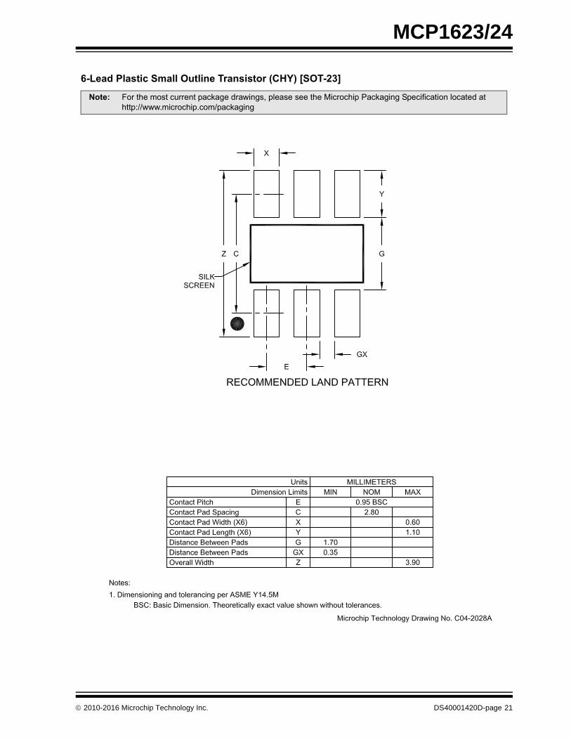
6-Lead Plastic Small Outline Transistor (CHY) [SOT-23]
Notes:1. Dimensions D and E1 do not include mold flash or protrusions. Mold flash or protrusions shall not exceed 0.127 mm per side.2. Dimensioning and tolerancing per ASME Y14.5M.
BSC: Basic Dimension. Theoretically exact value shown without tolerances.
Note: For the most current package drawings, please see the Microchip Packaging Specification located at http://www.microchip.com/packaging
Units MILLIMETERSDimension Limits MIN NOM MAX
Number of Pins N 6Pitch e 0.95 BSCOutside Lead Pitch e1 1.90 BSCOverall Height A 0.90 – 1.45Molded Package Thickness A2 0.89 – 1.30Standoff A1 0.00 – 0.15Overall Width E 2.20 – 3.20Molded Package Width E1 1.30 – 1.80Overall Length D 2.70 – 3.10Foot Length L 0.10 – 0.60Footprint L1 0.35 – 0.80Foot Angle 0° – 30°Lead Thickness c 0.08 – 0.26Lead Width b 0.20 – 0.51
b
E
4N
E1
PIN 1 ID BYLASER MARK
D
1 2 3
e
e1
A
A1
A2 c
L
L1
φ
Microchip Technology Drawing C04-028B
DS40001420D-page 20 2010-2016 Microchip Technology Inc.
MCP1623/24
6-Lead Plastic Small Outline Transistor (CHY) [SOT-23]
Note: For the most current package drawings, please see the Microchip Packaging Specification located at http://www.microchip.com/packaging
2010-2016 Microchip Technology Inc. DS40001420D-page 21

MCP1623/24
���������� ��������������������������������������!"�##�$��%�&���'
�����*�� ��������!"�����# $�% �&"� �'�������(�)"&�'"!&�) �����& #�*�&����&� ���&�� #��� ���� ���+�� �'������ ��� ����'�� � $�! #�&� �)��!��&� �#!�;� ���+�� ��!�!�*�!���"��& #��� ��' �!���������#�&�� �������� �����<�=���>��
?�@G ?�!�����' �!������� �� &������� $��&����" �!��*��*�&��"&�&�� ���� !��<JG � % � �� ���' �!���(�"!"�����*�&��"&�&�� ���� (�%�����%��'�&����"��! !������
����* J���&� �'�!&��"�� �&���+�� �#��*���!(�� �! �! �&� �������������+������� ��%���&��������& #��&��&&GKK***�'����������'K��+�����
V��&! ��ZZ��<�<����' �!����Z�'�&! ��[ [\� ��]
["') ���%����! [ ^��&�� ��>��?�@\� �����_ ���& � ��^� ���� �����&��#�%%� �� ���� ���� ���>@��&��&�����+� !! �; ������<J\� �����Z ��&� � �����?�@\� �����`�#&� < ;����?�@<$�! #���#�Z ��&� �� ��;� j ��>><$�! #���#�`�#&� <� ��>� j ���>@��&��&�`�#&� ) ���� ���> ��;�@��&��&�Z ��&� Z ��;� ���� ��>�@��&��&&�<$�! #���# q ���� j j
D
N
E
NOTE 1
1 2
EXPOSED PAD
NOTE 12 1
D2
K
L
E2
N
eb
A3 A1
A
NOTE 2
BOTTOM VIEWTOP VIEW
�������� � �������� ���*��� @����;@
DS40001420D-page 22 2010-2016 Microchip Technology Inc.

MCP1623/24
Note: For the most current package drawings, please see the Microchip Packaging Specification located at
http://www.microchip.com/packaging
2010-2016 Microchip Technology Inc. DS40001420D-page 23

MCP1623/24
NOTES:
DS40001420D-page 24 2010-2016 Microchip Technology Inc.

MCP1623/24
APPENDIX A: REVISION HISTORY
Revision D (September 2016)
The following is the list of modifications:
1. Minor modifications in DC Characteristics table(n-channel and p-channel max. leakage specs).
2. Minor typographical corrections.
Revision C (February 2011)
The following is the list of modifications:
1. Added the 8-lead, 2x3 DFN package and relatedinformation throughout the document.
2. Updated the package marking information anddrawings.
3. Updated the Product Identification Systempage.
Revision B (July 2010)
The following is the list of modifications:
1. Updated the packaging specification.
Revision A (May 2010)
• Initial release of the document.
2010-2016 Microchip Technology Inc. DS40001420D-page 25
MCP1623/24
NOTES:
DS40001420D-page 26 2010-2016 Microchip Technology Inc.

MCP1623/24
PRODUCT IDENTIFICATION SYSTEM
To order or obtain information, e.g., on pricing or delivery, refer to the factory or the listed sales office.
PART NO. X /XX
PackageTemperatureRange
Device
Device: MCP1623: 0.65V, PWM Only True Disconnect, Sync Boost Regulator
MCP1624: 0.65V, PWM/PFM True Disconnect, Sync Boost Regulator
Tape and Reel Option:
Blank = Standard packaging (tube or tray)T = Tape and Reel(1)
Temperature Range:
I = -40C to +85C (Industrial)
Package: CH = Plastic Small Outline Transistor (SOT-23), 6-leadCHY* = Plastic Small Outline Transistor (SOT-23), 6-leadMC = Plastic Dual Flat, No Lead (2x3 DFN), 8-lead
Y* = Nickel palladium gold manufacturing designator.Only available on the SOT-23 package.
Examples:
a) MCP1623T-I/CHY: Tape and Reel,0.65V, Sync Reg.,6LD SOT-23 package
b) MCP1624T-I/CHY: Tape and Reel,0.65V, Sync Reg.,6LD SOT-23 package
c) MCP1623-I/MC: 0.65V, Sync Reg.,8LD DFN package
d) MCP1623T-I/MC: Tape and Reel,0.65V, Sync Reg.,8LD DFN package
e) MCP1624-I/MC: 0.65V, Sync Reg.,8LD DFN package
f) MCP1624T-I/MC: Tape and Reel,0.65V, Sync Reg.,8LD DFN package
Note 1: Tape and Reel identifier only appears in the catalog part number description. This identi-fier is used for ordering purposes and is not printed on the device package. Check with your Microchip Sales Office for package availability with the Tape and Reel option.
[X](1)
Tape and ReelOption
2010-2016 Microchip Technology Inc. DS40001420D-page 27

MCP1623/24
NOTES:
DS40001420D-page 28 2010-2016 Microchip Technology Inc.
MCP1623/24
Note the following details of the code protection feature on Microchip devices:
• Microchip products meet the specification contained in their particular Microchip Data Sheet.
• Microchip believes that its family of products is one of the most secure families of its kind on the market today, when used in the intended manner and under normal conditions.
• There are dishonest and possibly illegal methods used to breach the code protection feature. All of these methods, to our knowledge, require using the Microchip products in a manner outside the operating specifications contained in Microchip’s Data Sheets. Most likely, the person doing so is engaged in theft of intellectual property.
• Microchip is willing to work with the customer who is concerned about the integrity of their code.
• Neither Microchip nor any other semiconductor manufacturer can guarantee the security of their code. Code protection does not mean that we are guaranteeing the product as “unbreakable.”
Code protection is constantly evolving. We at Microchip are committed to continuously improving the code protection features of ourproducts. Attempts to break Microchip’s code protection feature may be a violation of the Digital Millennium Copyright Act. If such actsallow unauthorized access to your software or other copyrighted work, you may have a right to sue for relief under that Act.
Information contained in this publication regarding deviceapplications and the like is provided only for your convenienceand may be superseded by updates. It is your responsibility toensure that your application meets with your specifications.MICROCHIP MAKES NO REPRESENTATIONS ORWARRANTIES OF ANY KIND WHETHER EXPRESS ORIMPLIED, WRITTEN OR ORAL, STATUTORY OROTHERWISE, RELATED TO THE INFORMATION,INCLUDING BUT NOT LIMITED TO ITS CONDITION,QUALITY, PERFORMANCE, MERCHANTABILITY ORFITNESS FOR PURPOSE. Microchip disclaims all liabilityarising from this information and its use. Use of Microchipdevices in life support and/or safety applications is entirely atthe buyer’s risk, and the buyer agrees to defend, indemnify andhold harmless Microchip from any and all damages, claims,suits, or expenses resulting from such use. No licenses areconveyed, implicitly or otherwise, under any Microchipintellectual property rights unless otherwise stated.
2010-2016 Microchip Technology Inc.
Microchip received ISO/TS-16949:2009 certification for its worldwide headquarters, design and wafer fabrication facilities in Chandler and Tempe, Arizona; Gresham, Oregon and design centers in California and India. The Company’s quality system processes and procedures are for its PIC® MCUs and dsPIC® DSCs, KEELOQ® code hopping devices, Serial EEPROMs, microperipherals, nonvolatile memory and analog products. In addition, Microchip’s quality system for the design and manufacture of development systems is ISO 9001:2000 certified.
QUALITY MANAGEMENT SYSTEM CERTIFIED BY DNV
== ISO/TS 16949 ==
Trademarks
The Microchip name and logo, the Microchip logo, AnyRate, dsPIC, FlashFlex, flexPWR, Heldo, JukeBlox, KeeLoq, KeeLoq logo, Kleer, LANCheck, LINK MD, MediaLB, MOST, MOST logo, MPLAB, OptoLyzer, PIC, PICSTART, PIC32 logo, RightTouch, SpyNIC, SST, SST Logo, SuperFlash and UNI/O are registered trademarks of Microchip Technology Incorporated in the U.S.A. and other countries.
ClockWorks, The Embedded Control Solutions Company, ETHERSYNCH, Hyper Speed Control, HyperLight Load, IntelliMOS, mTouch, Precision Edge, and QUIET-WIRE are registered trademarks of Microchip Technology Incorporated in the U.S.A.
Analog-for-the-Digital Age, Any Capacitor, AnyIn, AnyOut, BodyCom, chipKIT, chipKIT logo, CodeGuard, dsPICDEM, dsPICDEM.net, Dynamic Average Matching, DAM, ECAN, EtherGREEN, In-Circuit Serial Programming, ICSP, Inter-Chip Connectivity, JitterBlocker, KleerNet, KleerNet logo, MiWi, motorBench, MPASM, MPF, MPLAB Certified logo, MPLIB, MPLINK, MultiTRAK, NetDetach, Omniscient Code Generation, PICDEM, PICDEM.net, PICkit, PICtail, PureSilicon, RightTouch logo, REAL ICE, Ripple Blocker, Serial Quad I/O, SQI, SuperSwitcher, SuperSwitcher II, Total Endurance, TSHARC, USBCheck, VariSense, ViewSpan, WiperLock, Wireless DNA, and ZENA are trademarks of Microchip Technology Incorporated in the U.S.A. and other countries.
SQTP is a service mark of Microchip Technology Incorporated in the U.S.A.
Silicon Storage Technology is a registered trademark of Microchip Technology Inc. in other countries.
GestIC is a registered trademarks of Microchip Technology Germany II GmbH & Co. KG, a subsidiary of Microchip Technology Inc., in other countries.
All other trademarks mentioned herein are property of their respective companies.
© 2010-2016, Microchip Technology Incorporated, Printed in the U.S.A., All Rights Reserved.
ISBN: 978-1-5224-0920-5
DS40001420D-page 29
DS40001420D-page 30 2010-2016 Microchip Technology Inc.
AMERICASCorporate Office2355 West Chandler Blvd.Chandler, AZ 85224-6199Tel: 480-792-7200 Fax: 480-792-7277Technical Support: http://www.microchip.com/supportWeb Address: www.microchip.com
AtlantaDuluth, GA Tel: 678-957-9614 Fax: 678-957-1455
Austin, TXTel: 512-257-3370
BostonWestborough, MA Tel: 774-760-0087 Fax: 774-760-0088
ChicagoItasca, IL Tel: 630-285-0071 Fax: 630-285-0075
ClevelandIndependence, OH Tel: 216-447-0464 Fax: 216-447-0643
DallasAddison, TX Tel: 972-818-7423 Fax: 972-818-2924
DetroitNovi, MI Tel: 248-848-4000
Houston, TX Tel: 281-894-5983
IndianapolisNoblesville, IN Tel: 317-773-8323Fax: 317-773-5453
Los AngelesMission Viejo, CA Tel: 949-462-9523 Fax: 949-462-9608
New York, NY Tel: 631-435-6000
San Jose, CA Tel: 408-735-9110
Canada - TorontoTel: 905-695-1980 Fax: 905-695-2078
ASIA/PACIFICAsia Pacific OfficeSuites 3707-14, 37th FloorTower 6, The GatewayHarbour City, Kowloon
Hong KongTel: 852-2943-5100Fax: 852-2401-3431
Australia - SydneyTel: 61-2-9868-6733Fax: 61-2-9868-6755
China - BeijingTel: 86-10-8569-7000 Fax: 86-10-8528-2104
China - ChengduTel: 86-28-8665-5511Fax: 86-28-8665-7889
China - ChongqingTel: 86-23-8980-9588Fax: 86-23-8980-9500
China - DongguanTel: 86-769-8702-9880
China - GuangzhouTel: 86-20-8755-8029
China - HangzhouTel: 86-571-8792-8115 Fax: 86-571-8792-8116
China - Hong Kong SARTel: 852-2943-5100 Fax: 852-2401-3431
China - NanjingTel: 86-25-8473-2460Fax: 86-25-8473-2470
China - QingdaoTel: 86-532-8502-7355Fax: 86-532-8502-7205
China - ShanghaiTel: 86-21-5407-5533 Fax: 86-21-5407-5066
China - ShenyangTel: 86-24-2334-2829Fax: 86-24-2334-2393
China - ShenzhenTel: 86-755-8864-2200 Fax: 86-755-8203-1760
China - WuhanTel: 86-27-5980-5300Fax: 86-27-5980-5118
China - XianTel: 86-29-8833-7252Fax: 86-29-8833-7256
ASIA/PACIFICChina - XiamenTel: 86-592-2388138 Fax: 86-592-2388130
China - ZhuhaiTel: 86-756-3210040 Fax: 86-756-3210049
India - BangaloreTel: 91-80-3090-4444 Fax: 91-80-3090-4123
India - New DelhiTel: 91-11-4160-8631Fax: 91-11-4160-8632
India - PuneTel: 91-20-3019-1500
Japan - OsakaTel: 81-6-6152-7160 Fax: 81-6-6152-9310
Japan - TokyoTel: 81-3-6880- 3770 Fax: 81-3-6880-3771
Korea - DaeguTel: 82-53-744-4301Fax: 82-53-744-4302
Korea - SeoulTel: 82-2-554-7200Fax: 82-2-558-5932 or 82-2-558-5934
Malaysia - Kuala LumpurTel: 60-3-6201-9857Fax: 60-3-6201-9859
Malaysia - PenangTel: 60-4-227-8870Fax: 60-4-227-4068
Philippines - ManilaTel: 63-2-634-9065Fax: 63-2-634-9069
SingaporeTel: 65-6334-8870Fax: 65-6334-8850
Taiwan - Hsin ChuTel: 886-3-5778-366Fax: 886-3-5770-955
Taiwan - KaohsiungTel: 886-7-213-7828
Taiwan - TaipeiTel: 886-2-2508-8600 Fax: 886-2-2508-0102
Thailand - BangkokTel: 66-2-694-1351Fax: 66-2-694-1350
EUROPEAustria - WelsTel: 43-7242-2244-39Fax: 43-7242-2244-393
Denmark - CopenhagenTel: 45-4450-2828 Fax: 45-4485-2829
France - ParisTel: 33-1-69-53-63-20 Fax: 33-1-69-30-90-79
Germany - DusseldorfTel: 49-2129-3766400
Germany - KarlsruheTel: 49-721-625370
Germany - MunichTel: 49-89-627-144-0 Fax: 49-89-627-144-44
Italy - Milan Tel: 39-0331-742611 Fax: 39-0331-466781
Italy - VeniceTel: 39-049-7625286
Netherlands - DrunenTel: 31-416-690399 Fax: 31-416-690340
Poland - WarsawTel: 48-22-3325737
Spain - MadridTel: 34-91-708-08-90Fax: 34-91-708-08-91
Sweden - StockholmTel: 46-8-5090-4654
UK - WokinghamTel: 44-118-921-5800Fax: 44-118-921-5820
Worldwide Sales and Service
06/23/16