Embed Size (px)
Citation preview
MCP2561/2FDHigh-Speed CAN Flexible Data Rate Transceiver
Features: • Optimized for CAN FD (Flexible Data rate) at 2, 5
and 8 Mbps Operation- Maximum Propagation Delay: 120 ns- Loop Delay Symmetry: -10%/+10% (2 Mbps)
• Implements ISO-11898-2 and ISO-11898-5 Standard Physical Layer Requirements
• Very Low Standby Current (5 µA, typical)• VIO Supply Pin to Interface Directly to
CAN Controllers and Microcontrollers with 1.8V to 5.5V I/O
• SPLIT Output Pin to Stabilize Common Mode in Biased Split Termination Schemes
• CAN Bus Pins are Disconnected when Device is Unpowered- An Unpowered Node or Brown-Out Event will
Not Load the CAN Bus• Detection of Ground Fault:
- Permanent Dominant Detection on TXD
- Permanent Dominant Detection on Bus• Power-on Reset and Voltage Brown-Out
Protection on VDD Pin• Protection Against Damage Due to Short-Circuit
Conditions (Positive or Negative Battery Voltage)• Protection Against High-Voltage Transients in
Automotive Environments• Automatic Thermal Shutdown Protection• Suitable for 12V and 24V Systems• Meets or exceeds stringent automotive design
requirements including “Hardware Requirements for LIN, CAN and FlexRay Interfaces in Automotive Applications”, Version 1.3, May 2012- Radiated emissions @ 2 Mbps with Common
Mode Choke (CMC)- DPI @ 2 Mbps with CMC
• High ESD Protection on CANH and CANL, meeting IEC61000-4-2 up to ±14 kV
• Available in PDIP-8L, SOIC-8L and 3x3 DFN-8L• Temperature ranges:
- Extended (E): -40°C to +125°C- High (H): -40°C to +150°C
Description:The MCP2561/2FD is a second generation high-speed CAN transceiver from Microchip Technology Inc. It offers the same features as the MCP2561/2. Additionally, it guarantees Loop Delay Symmetry in order to support the higher data rates required for CAN FD. The maximum propagation delay was improved to support longer bus length.The device meets the automotive requirements for CAN FD bit rates exceeding 2 Mbps, low quiescent current, electromagnetic compatibility (EMC) and electrostatic discharge (ESD).
Package Types
MCP2561/2FD Family Members
MCP2562FDPDIP, SOIC
VDD
VSS
RXD
CANH
CANL
1
2
34
8
7
65 VIO
STBYTXD
MCP2561FDPDIP, SOIC
VDD
VSS
RXD
CANH
CANL
1
2
34
8
7
65 SPLIT
STBYTXD
MCP2561FD3x3 DFN*
VDD
VSS
RXD
CANH
CANL
1
2
3
4
8
7
6
5 SPLIT
STBYTXD
EP9
MCP2562FD3x3 DFN*
VDD
VSS
RXD
CANH
CANL
1
2
3
4
8
7
6
5 VIO
STBYTXD
EP9
* Includes Exposed Thermal Pad (EP); see Table 1-2
Device Feature Description
MCP2561FD SPLIT pin Common mode stabilizationMCP2562FD VIO pin Internal level shifter on digital I/O pins
Note: For ordering information, see the “Product Identification System” section on page 29.
2014 Microchip Technology Inc. DS20005284A-page 1
MCP2561/2FD
Block DiagramNote 1: There is only one receiver implemented. The receiver can operate in Low-Power or High-Speed mode.
2: Only MCP2561FD has the SPLIT pin.
3: Only MCP2562FD has the VIO pin. In MCP2561FD, the supply for the digital I/O is internally connected to VDD.
VDD
CANH
CANL
TXD
RXD
Driverand
Slope Control
ThermalProtection
PORUVLO
Digital I/OSupply
VIO(3)
VSS
STBY
PermanentDominant Detect
VIO
VIO
ModeControl
VDD/2
SPLIT(2 )
Wake-UpFilter
CANH
CANL
CANH
CANL
Receiver
LP_RX(1)
HS_RX
DS20005284A-page 2 2014 Microchip Technology Inc.
MCP2561/2FD
1.0 DEVICE OVERVIEWThe MCP2561/2FD is a high-speed CAN device, fault-tolerant device that serves as the interface between a CAN protocol controller and the physical bus. The MCP2561/2FD device provides differential transmit and receive capability for the CAN protocol controller, and is fully compatible with the ISO-11898-2 and ISO-11898-5 standards.
The Loop Delay Symmetry is guaranteed to support data rates that are up to 5 Mbps for CAN FD (Flexible Data rate). The maximum propagation delay was improved to support longer bus length.
Typically, each node in a CAN system must have a device to convert the digital signals generated by a CAN controller to signals suitable for transmission over the bus cabling (differential output). It also provides a buffer between the CAN controller and the high-voltage spikes that can be generated on the CAN bus by outside sources.
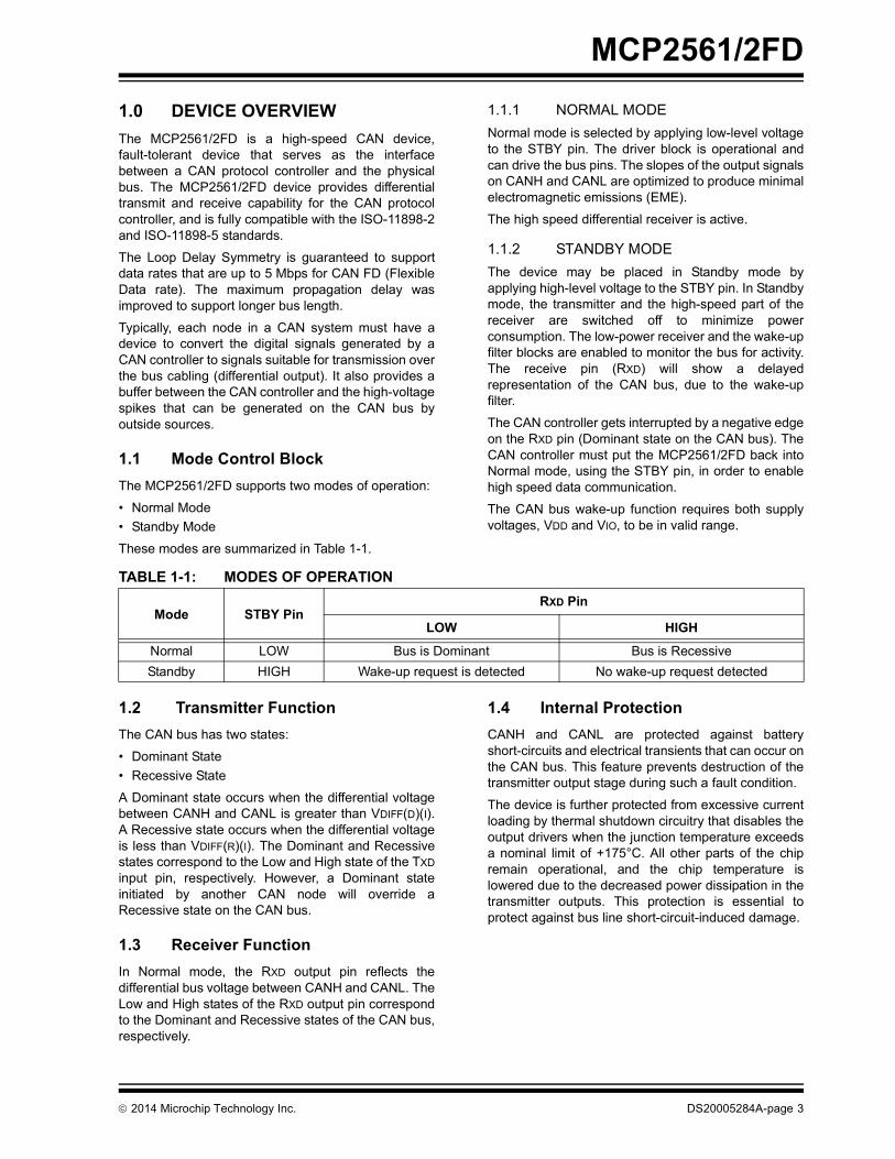
1.1 Mode Control BlockThe MCP2561/2FD supports two modes of operation:
• Normal Mode• Standby Mode
These modes are summarized in Table 1-1.
1.1.1 NORMAL MODENormal mode is selected by applying low-level voltage to the STBY pin. The driver block is operational and can drive the bus pins. The slopes of the output signals on CANH and CANL are optimized to produce minimal electromagnetic emissions (EME).
The high speed differential receiver is active.
1.1.2 STANDBY MODEThe device may be placed in Standby mode by applying high-level voltage to the STBY pin. In Standby mode, the transmitter and the high-speed part of the receiver are switched off to minimize power consumption. The low-power receiver and the wake-up filter blocks are enabled to monitor the bus for activity. The receive pin (RXD) will show a delayed representation of the CAN bus, due to the wake-up filter.
The CAN controller gets interrupted by a negative edge on the RXD pin (Dominant state on the CAN bus). The CAN controller must put the MCP2561/2FD back into Normal mode, using the STBY pin, in order to enable high speed data communication.
The CAN bus wake-up function requires both supply voltages, VDD and VIO, to be in valid range.
1.2 Transmitter FunctionThe CAN bus has two states:
• Dominant State• Recessive State
A Dominant state occurs when the differential voltage between CANH and CANL is greater than VDIFF(D)(I). A Recessive state occurs when the differential voltage is less than VDIFF(R)(I). The Dominant and Recessive states correspond to the Low and High state of the TXDinput pin, respectively. However, a Dominant state initiated by another CAN node will override a Recessive state on the CAN bus.
1.3 Receiver FunctionIn Normal mode, the RXD output pin reflects the differential bus voltage between CANH and CANL. The Low and High states of the RXD output pin correspond to the Dominant and Recessive states of the CAN bus, respectively.
1.4 Internal ProtectionCANH and CANL are protected against battery short-circuits and electrical transients that can occur on the CAN bus. This feature prevents destruction of the transmitter output stage during such a fault condition.
The device is further protected from excessive current loading by thermal shutdown circuitry that disables the output drivers when the junction temperature exceeds a nominal limit of +175°C. All other parts of the chip remain operational, and the chip temperature is lowered due to the decreased power dissipation in the transmitter outputs. This protection is essential to protect against bus line short-circuit-induced damage.
TABLE 1-1: MODES OF OPERATION
Mode STBY PinRXD Pin
LOW HIGH
Normal LOW Bus is Dominant Bus is RecessiveStandby HIGH Wake-up request is detected No wake-up request detected
2014 Microchip Technology Inc. DS20005284A-page 3
MCP2561/2FD
1.5 Permanent Dominant Detection The MCP2561/2FD device prevents two conditions:• Permanent Dominant condition on TXD
• Permanent Dominant condition on the bus
In Normal mode, if the MCP2561/2FD detects an extended Low state on the TXD input, it will disable the CANH and CANL output drivers in order to prevent the corruption of data on the CAN bus. The drivers will remain disabled until TXD goes High.
In Standby mode, if the MCP2561/2FD detects an extended Dominant condition on the bus, it will set the RXD pin to Recessive state. This allows the attached controller to go to Low-Power mode until the Dominant issue is corrected. RXD is latched High until a Recessive state is detected on the bus, and the wake-up function is enabled again.
Both conditions have a time-out of 1.25 ms (typical). This implies a maximum bit time of 69.44 µs (14.4 kHz), allowing up to 18 consecutive dominant bits on the bus.
1.6 Power-On Reset (POR) and Undervoltage Detection
The MCP2561/2FD has undervoltage detection on both supply pins: VDD and VIO. Typical undervoltage thresholds are 1.2V for VIO and 4V for VDD.
When the device is powered on, CANH and CANL remain in a high-impedance state until both VDD and VIO exceed their undervoltage levels. Once powered on, CANH and CANL will enter a high-impedance state if the voltage level at VDD drops below the undervoltage level, providing voltage brown-out protection during normal operation.
In Normal mode, the receiver output is forced to Recessive state during an undervoltage condition on VDD. In Standby mode, the low-power receiver is only enabled when both VDD and VIO supply voltages rise above their respective undervoltage thresholds. Once these threshold voltages are reached, the low-power receiver is no longer controlled by the POR comparator and remains operational down to about 2.5V on the VDD supply (MCP2561/2FD). The MCP2562FD transfers data to the RXD pin down to 1.8V on the VIOsupply.
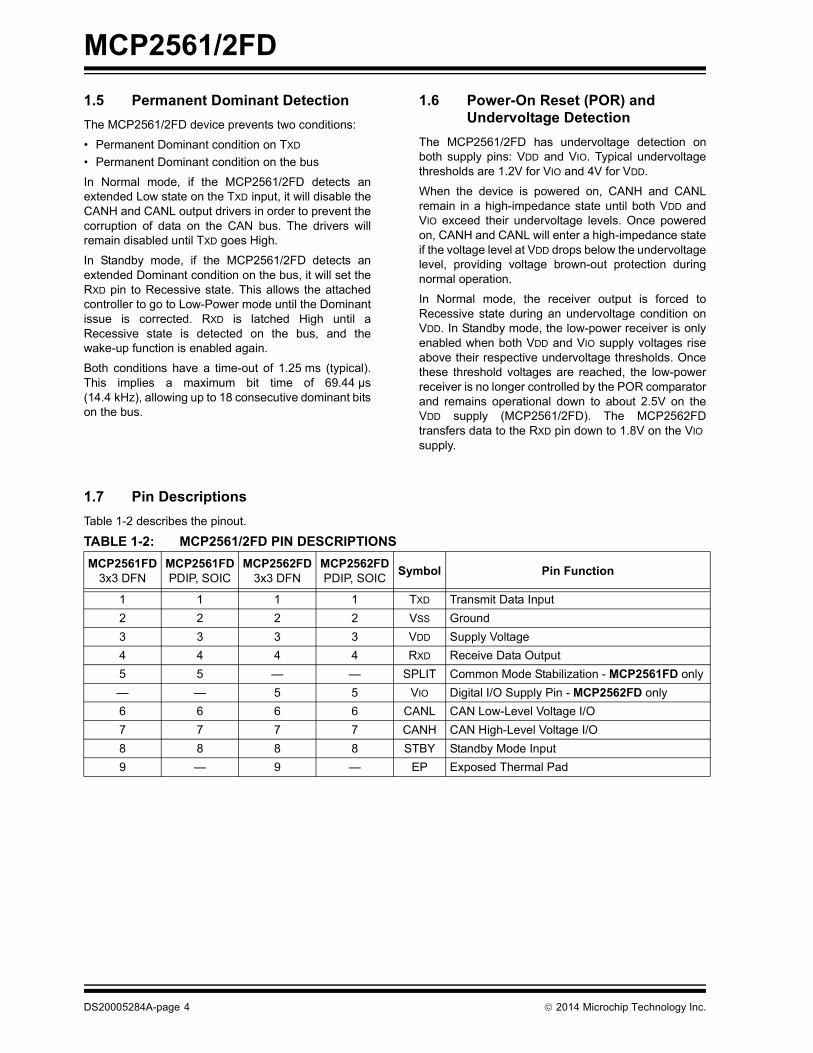
1.7 Pin DescriptionsTable 1-2 describes the pinout.
TABLE 1-2: MCP2561/2FD PIN DESCRIPTIONSMCP2561FD
3x3 DFNMCP2561FDPDIP, SOIC
MCP2562FD3x3 DFN
MCP2562FDPDIP, SOIC Symbol Pin Function
1 1 1 1 TXD Transmit Data Input2 2 2 2 VSS Ground3 3 3 3 VDD Supply Voltage4 4 4 4 RXD Receive Data Output5 5 — — SPLIT Common Mode Stabilization - MCP2561FD only— — 5 5 VIO Digital I/O Supply Pin - MCP2562FD only6 6 6 6 CANL CAN Low-Level Voltage I/O7 7 7 7 CANH CAN High-Level Voltage I/O8 8 8 8 STBY Standby Mode Input9 — 9 — EP Exposed Thermal Pad
DS20005284A-page 4 2014 Microchip Technology Inc.
MCP2561/2FD
1.7.1 TRANSMITTER DATAINPUT PIN (TXD)The CAN transceiver drives the differential output pins CANH and CANL according to TXD. It is usually connected to the transmitter data output of the CAN controller device. When TXD is Low, CANH and CANL are in the Dominant state. When TXD is High, CANH and CANL are in the Recessive state, provided that another CAN node is not driving the CAN bus with a Dominant state. TXD is connected to an internal pull-up resistor (nominal 33 k) to VDD or VIO, in the MCP2561FD or MCP2562FD, respectively.
1.7.2 GROUND SUPPLY PIN (VSS)Ground supply pin.
1.7.3 SUPPLY VOLTAGE PIN (VDD)Positive supply voltage pin. Supplies transmitter and receiver, including the wake-up receiver.
1.7.4 RECEIVER DATA OUTPUT PIN (RXD)
RXD is a CMOS-compatible output that drives High or Low depending on the differential signals on the CANH and CANL pins, and is usually connected to the receiver data input of the CAN controller device. RXD is High when the CAN bus is Recessive, and Low in the Dominant state. RXD is supplied by VDD or VIO, in the MCP2561FD or MCP2562FD, respectively.
1.7.5 SPLIT PIN (MCP2561FD ONLY)Reference Voltage Output (defined as VDD/2). The pin is only active in Normal mode. In Standby mode, or when VDD is off, SPLIT floats.
1.7.6 VIO PIN (MCP2562FD ONLY)Supply for digital I/O pins. In the MCP2561FD, the supply for the digital I/O (TXD, RXD and STBY) is internally connected to VDD.
1.7.7 CAN LOW PIN (CANL)The CANL output drives the Low side of the CAN differential bus. This pin is also tied internally to the receive input comparator. CANL disconnects from the bus when MCP2561/2FD is not powered.
1.7.8 CAN HIGH PIN (CANH)The CANH output drives the high-side of the CAN differential bus. This pin is also tied internally to the receive input comparator. CANH disconnects from the bus when MCP2561/2FD is not powered.
1.7.9 STANDBY MODE INPUT PIN (STBY)This pin selects between Normal or Standby mode. In Standby mode, the transmitter, high speed receiver and SPLIT are turned off, only the low power receiver and wake-up filter are active. STBY is connected to an internal MOS pull-up resistor to VDD or VIO, in the MCP2561FD or MCP2562FD, respectively. The value of the MOS pull-up resistor depends on the supply volt-age. Typical values are 660 k for 5V, 1.1 M for 3.3V and 4.4 M for 1.8V
1.7.10 EXPOSED THERMAL PAD (EP)It is recommended that this pad is connected to VSS for the enhancement of electromagnetic immunity and thermal resistance.
2014 Microchip Technology Inc. DS20005284A-page 5
MCP2561/2FD
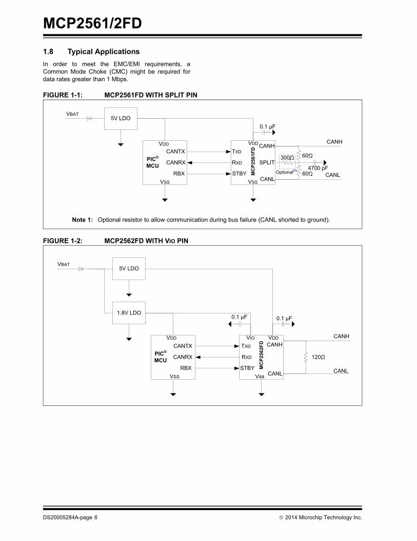
1.8 Typical ApplicationsIn order to meet the EMC/EMI requirements, a Common Mode Choke (CMC) might be required for data rates greater than 1 Mbps.FIGURE 1-1: MCP2561FD WITH SPLIT PIN
FIGURE 1-2: MCP2562FD WITH VIO PIN
5V LDO
VDD VDD
TXD
RXD
STBY
CANTX
CANRX
RBXVSS VSS
PIC®
MCU
MC
P256
1FD
SPLIT
CANH
CANL4700 pF
0.1 μF
CANH
CANL60
60300
Optional(1)
VBAT
Note 1: Optional resistor to allow communication during bus failure (CANL shorted to ground).
1.8V LDO
VDD VDD
TXD
RXD
STBY
CANTX
CANRX
RBXVSS Vss
PIC®
MCU
MC
P256
2FD
CANH
CANL
5V LDO
VIO
0.1 μF
CANH
CANL
0.1 μF
120
VBAT
DS20005284A-page 6 2014 Microchip Technology Inc.
MCP2561/2FD
2.0 ELECTRICAL CHARACTERISTICS
2.1 Terms and DefinitionsA number of terms are defined in ISO-11898 that are used to describe the electrical characteristics of a CAN transceiver device. These terms and definitions are summarized in this section.
2.1.1 BUS VOLTAGEVCANL and VCANH denote the voltages of the bus line wires CANL and CANH relative to ground of each individual CAN node.
2.1.2 COMMON MODE BUS VOLTAGE RANGE
Boundary voltage levels of VCANL and VCANH with respect to ground, for which proper operation will occur, if up to the maximum number of CAN nodes are connected to the bus.
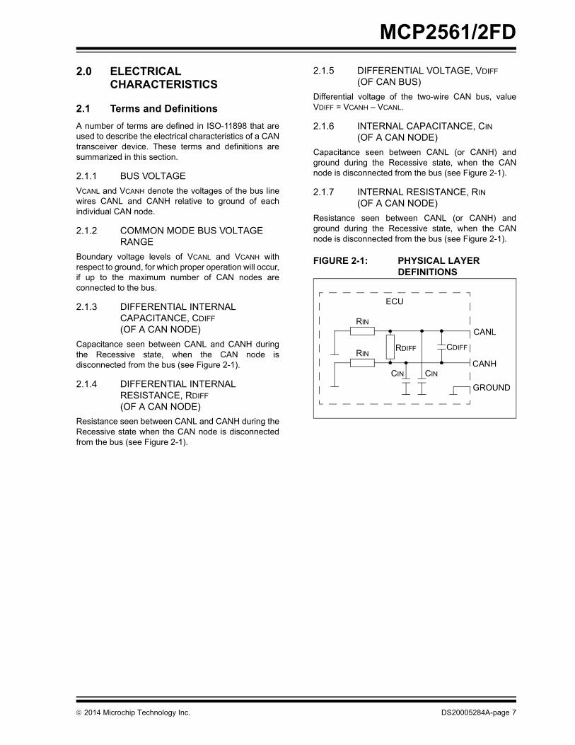
2.1.3 DIFFERENTIAL INTERNAL CAPACITANCE, CDIFF (OF A CAN NODE)
Capacitance seen between CANL and CANH during the Recessive state, when the CAN node is disconnected from the bus (see Figure 2-1).
2.1.4 DIFFERENTIAL INTERNAL RESISTANCE, RDIFF (OF A CAN NODE)
Resistance seen between CANL and CANH during the Recessive state when the CAN node is disconnected from the bus (see Figure 2-1).
2.1.5 DIFFERENTIAL VOLTAGE, VDIFF (OF CAN BUS)
Differential voltage of the two-wire CAN bus, value VDIFF = VCANH – VCANL.
2.1.6 INTERNAL CAPACITANCE, CIN (OF A CAN NODE)
Capacitance seen between CANL (or CANH) and ground during the Recessive state, when the CAN node is disconnected from the bus (see Figure 2-1).
2.1.7 INTERNAL RESISTANCE, RIN (OF A CAN NODE)
Resistance seen between CANL (or CANH) and ground during the Recessive state, when the CAN node is disconnected from the bus (see Figure 2-1).
FIGURE 2-1: PHYSICAL LAYER DEFINITIONS
RIN
RINRDIFF
CIN CIN
CDIFF
CANL
CANH
GROUND
ECU
2014 Microchip Technology Inc. DS20005284A-page 7
MCP2561/2FD
2.2 Absolute Maximum Ratings†VDD.............................................................................................................................................................................7.0VVIO..............................................................................................................................................................................7.0V
DC Voltage at TXD, RXD, STBY and VSS.............................................................................................-0.3V to VIO + 0.3V
DC Voltage at CANH, CANL and SPLIT ...................................................................................................... -58V to +58V
Transient Voltage on CANH, CANL (ISO-7637) (See Figure 2-5)............................................................ -150V to +100V
Storage temperature ...............................................................................................................................-55°C to +150°C
Operating ambient temperature ..............................................................................................................-40°C to +150°C
Virtual Junction Temperature, TVJ (IEC60747-1) ....................................................................................-40°C to +190°C
Soldering temperature of leads (10 seconds) .......................................................................................................+300°C
ESD protection on CANH and CANL pins for MCP2561FD (IEC 61000-4-2) ........................................................±14 kV
ESD protection on CANH and CANL pins for MCP2562FD (IEC 61000-4-2) ..........................................................±8 kV
ESD protection on CANH and CANL pins (IEC 801; Human Body Model)..............................................................±8 kV
ESD protection on all other pins (IEC 801; Human Body Model).............................................................................±4 kV
ESD protection on all pins (IEC 801; Machine Model) ............................................................................................±300V
ESD protection on all pins (IEC 801; Charge Device Model) ..................................................................................±750V
† NOTICE: Stresses above those listed under “Maximum ratings” may cause permanent damage to the device. This is a stress rating only and functional operation of the device at those or any other conditions above those indicated in the operational listings of this specification is not implied. Exposure to maximum rating conditions for extended periods may affect device reliability.
DS20005284A-page 8 2014 Microchip Technology Inc.
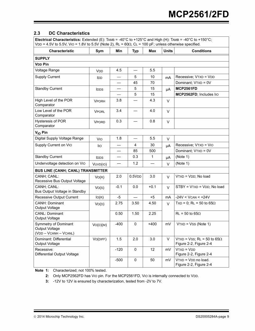
MCP2561/2FD
2.3 DC Characteristics Electrical Characteristics: Extended (E): TAMB = -40°C to +125°C and High (H): TAMB = -40°C to +150°C; VDD = 4.5V to 5.5V, VIO = 1.8V to 5.5V (Note 2), RL = 60, CL = 100 pF; unless otherwise specified.
Characteristic Sym Min Typ Max Units Conditions
SUPPLYVDD PinVoltage Range VDD 4.5 — 5.5
Supply Current IDD — 5 10 mA Recessive; VTXD = VDD
— 45 70 Dominant; VTXD = 0VStandby Current IDDS — 5 15 µA MCP2561FD
— 5 15 MCP2562FD; Includes IIOHigh Level of the POR Comparator
VPORH 3.8 — 4.3 V
Low Level of the POR Comparator
VPORL 3.4 — 4.0 V
Hysteresis of POR Comparator
VPORD 0.3 — 0.8 V
VIO PinDigital Supply Voltage Range VIO 1.8 — 5.5 VSupply Current on VIO IIO — 4 30 µA Recessive; VTXD = VIO
— 85 500 Dominant; VTXD = 0VStandby Current IDDS — 0.3 1 µA (Note 1)
Undervoltage detection on VIO VUVD(IO) — 1.2 — V (Note 1)
BUS LINE (CANH; CANL) TRANSMITTERCANH; CANL: Recessive Bus Output Voltage
VO(R) 2.0 0.5VDD 3.0 V VTXD = VDD; No load
CANH; CANL: Bus Output Voltage in Standby
VO(S) -0.1 0.0 +0.1 V STBY = VTXD = VDD; No load
Recessive Output Current IO(R) -5 — +5 mA -24V < VCAN < +24VCANH: Dominant Output Voltage
VO(D) 2.75 3.50 4.50 V TXD = 0; RL = 50 to 65
CANL: Dominant Output Voltage
0.50 1.50 2.25 RL = 50 to 65
Symmetry of Dominant Output Voltage (VDD – VCANH – VCANL)
VO(D)(M) -400 0 +400 mV VTXD = VSS (Note 1)
Dominant: Differential Output Voltage
VO(DIFF) 1.5 2.0 3.0 V VTXD = VSS; RL = 50 to 65Figure 2-2, Figure 2-4
Recessive: Differential Output Voltage
-120 0 12 mV VTXD = VDDFigure 2-2, Figure 2-4
-500 0 50 mV VTXD = VDD,no load.Figure 2-2, Figure 2-4
Note 1: Characterized; not 100% tested.2: Only MCP2562FD has VIO pin. For the MCP2561FD, VIO is internally connected to VDD. 3: -12V to 12V is ensured by characterization, tested from -2V to 7V.
2014 Microchip Technology Inc. DS20005284A-page 9
MCP2561/2FD
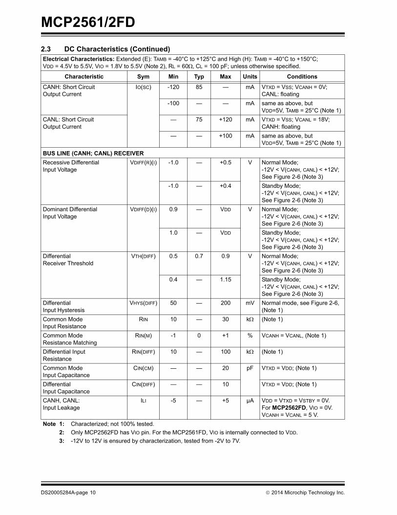
CANH: Short Circuit Output Current
IO(SC) -120 85 — mA VTXD = VSS; VCANH = 0V;CANL: floating
-100 — — mA same as above, butVDD=5V, TAMB = 25°C (Note 1)
CANL: Short Circuit Output Current
— 75 +120 mA VTXD = VSS; VCANL = 18V; CANH: floating
— — +100 mA same as above, butVDD=5V, TAMB = 25°C (Note 1)
BUS LINE (CANH; CANL) RECEIVERRecessive Differential Input Voltage
VDIFF(R)(I) -1.0 — +0.5 V Normal Mode;-12V < V(CANH, CANL) < +12V;See Figure 2-6 (Note 3)
-1.0 — +0.4 Standby Mode;-12V < V(CANH, CANL) < +12V;See Figure 2-6 (Note 3)
Dominant Differential Input Voltage
VDIFF(D)(I) 0.9 — VDD V Normal Mode;-12V < V(CANH, CANL) < +12V;See Figure 2-6 (Note 3)
1.0 — VDD Standby Mode;-12V < V(CANH, CANL) < +12V;See Figure 2-6 (Note 3)
Differential Receiver Threshold
VTH(DIFF) 0.5 0.7 0.9 V Normal Mode;-12V < V(CANH, CANL) < +12V;See Figure 2-6 (Note 3)
0.4 — 1.15 Standby Mode;-12V < V(CANH, CANL) < +12V;See Figure 2-6 (Note 3)
Differential Input Hysteresis
VHYS(DIFF) 50 — 200 mV Normal mode, see Figure 2-6, (Note 1)
Common Mode Input Resistance
RIN 10 — 30 k (Note 1)
Common Mode Resistance Matching
RIN(M) -1 0 +1 % VCANH = VCANL, (Note 1)
Differential Input Resistance
RIN(DIFF) 10 — 100 k (Note 1)
Common Mode Input Capacitance
CIN(CM) — — 20 pF VTXD = VDD; (Note 1)
Differential Input Capacitance
CIN(DIFF) — — 10 VTXD = VDD; (Note 1)
CANH, CANL: Input Leakage
ILI -5 — +5 µA VDD = VTXD = VSTBY = 0V.For MCP2562FD, VIO = 0V.VCANH = VCANL = 5 V.
2.3 DC Characteristics (Continued)Electrical Characteristics: Extended (E): TAMB = -40°C to +125°C and High (H): TAMB = -40°C to +150°C; VDD = 4.5V to 5.5V, VIO = 1.8V to 5.5V (Note 2), RL = 60, CL = 100 pF; unless otherwise specified.
Characteristic Sym Min Typ Max Units Conditions
Note 1: Characterized; not 100% tested.2: Only MCP2562FD has VIO pin. For the MCP2561FD, VIO is internally connected to VDD. 3: -12V to 12V is ensured by characterization, tested from -2V to 7V.
DS20005284A-page 10 2014 Microchip Technology Inc.
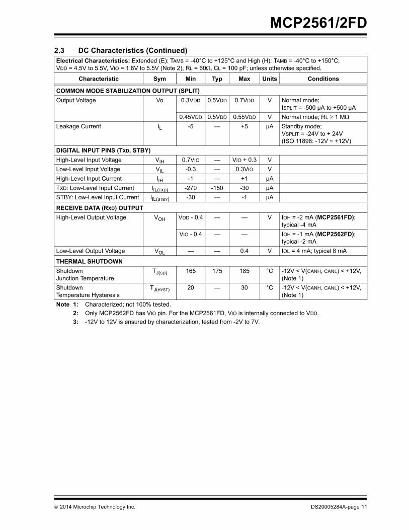
MCP2561/2FD
COMMON MODE STABILIZATION OUTPUT (SPLIT)Output Voltage Vo 0.3VDD 0.5VDD 0.7VDD V Normal mode;
ISPLIT = -500 µA to +500 µA0.45VDD 0.5VDD 0.55VDD V Normal mode; RL 1 M
Leakage Current IL -5 — +5 µA Standby mode; VSPLIT = -24V to + 24V (ISO 11898: -12V ~ +12V)
DIGITAL INPUT PINS (TXD, STBY)High-Level Input Voltage VIH 0.7VIO — VIO + 0.3 VLow-Level Input Voltage VIL -0.3 — 0.3VIO VHigh-Level Input Current IIH -1 — +1 µATXD: Low-Level Input Current IIL(TXD) -270 -150 -30 µASTBY: Low-Level Input Current IIL(STBY) -30 — -1 µA
RECEIVE DATA (RXD) OUTPUTHigh-Level Output Voltage VOH VDD - 0.4 — — V IOH = -2 mA (MCP2561FD);
typical -4 mAVIO - 0.4 — — IOH = -1 mA (MCP2562FD);
typical -2 mALow-Level Output Voltage VOL — — 0.4 V IOL = 4 mA; typical 8 mA
THERMAL SHUTDOWNShutdown Junction Temperature
TJ(SD) 165 175 185 °C -12V < V(CANH, CANL) < +12V,(Note 1)
Shutdown Temperature Hysteresis
TJ(HYST) 20 — 30 °C -12V < V(CANH, CANL) < +12V,(Note 1)
2.3 DC Characteristics (Continued)Electrical Characteristics: Extended (E): TAMB = -40°C to +125°C and High (H): TAMB = -40°C to +150°C; VDD = 4.5V to 5.5V, VIO = 1.8V to 5.5V (Note 2), RL = 60, CL = 100 pF; unless otherwise specified.
Characteristic Sym Min Typ Max Units Conditions
Note 1: Characterized; not 100% tested.2: Only MCP2562FD has VIO pin. For the MCP2561FD, VIO is internally connected to VDD. 3: -12V to 12V is ensured by characterization, tested from -2V to 7V.
2014 Microchip Technology Inc. DS20005284A-page 11
MCP2561/2FD
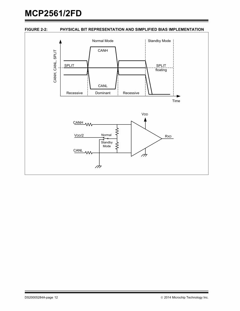
FIGURE 2-2: PHYSICAL BIT REPRESENTATION AND SIMPLIFIED BIAS IMPLEMENTATIONCA
NH
,CA
NL,
SP
LIT
Time
CANH
CANL
SPLIT
Normal Mode Standby Mode
Recessive RecessiveDominant
SPLITfloating
CANL
CANH
VDD/2 RXD
VDD
Normal
StandbyMode
DS20005284A-page 12 2014 Microchip Technology Inc.
MCP2561/2FD
FIGURE 2-3: TEST LOAD CONDITIONS
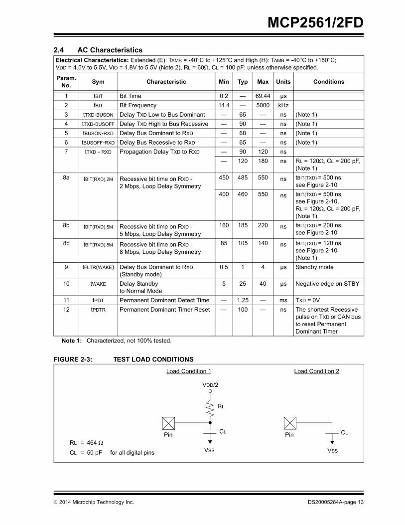
2.4 AC Characteristics Electrical Characteristics: Extended (E): TAMB = -40°C to +125°C and High (H): TAMB = -40°C to +150°C; VDD = 4.5V to 5.5V, VIO = 1.8V to 5.5V (Note 2), RL = 60CL = 100 pF; unless otherwise specified.
Param. No. Sym Characteristic Min Typ Max Units Conditions
1 tBIT Bit Time 0.2 — 69.44 µs2 fBIT Bit Frequency 14.4 — 5000 kHz3 tTXD-BUSON Delay TXD Low to Bus Dominant — 65 — ns (Note 1)4 tTXD-BUSOFF Delay TXD High to Bus Recessive — 90 — ns (Note 1)5 tBUSON-RXD Delay Bus Dominant to RXD — 60 — ns (Note 1)6 tBUSOFF-RXD Delay Bus Recessive to RXD — 65 — ns (Note 1)7 tTXD - RXD Propagation Delay TXD to RXD — 90 120 ns
— 120 180 ns RL = 120CL = 200 pF, (Note 1)
8a tBIT(RXD),2M Recessive bit time on RXD - 2 Mbps, Loop Delay Symmetry
450 485 550 ns tBIT(TXD) = 500 ns,see Figure 2-10
400 460 550 ns tBIT(TXD) = 500 ns,see Figure 2-10, RL = 120CL = 200 pF, (Note 1)
8b tBIT(RXD),5M Recessive bit time on RXD - 5 Mbps, Loop Delay Symmetry
160 185 220 ns tBIT(TXD) = 200 ns,see Figure 2-10
8c tBIT(RXD),8M Recessive bit time on RXD - 8 Mbps, Loop Delay Symmetry
85 105 140 ns tBIT(TXD) = 120 ns,see Figure 2-10(Note 1)
9 tFLTR(WAKE) Delay Bus Dominant to RXD (Standby mode)
0.5 1 4 µs Standby mode
10 tWAKE Delay Standby to Normal Mode
5 25 40 µs Negative edge on STBY
11 tPDT Permanent Dominant Detect Time — 1.25 — ms TXD = 0V12 tPDTR Permanent Dominant Timer Reset — 100 — ns The shortest Recessive
pulse on TXD or CAN bus to reset Permanent Dominant Timer
Note 1: Characterized, not 100% tested.
VDD/2
CL
RL
Pin Pin
VSS VSS
CL
RL = 464
CL = 50 pF for all digital pins
Load Condition 1 Load Condition 2
2014 Microchip Technology Inc. DS20005284A-page 13
MCP2561/2FD
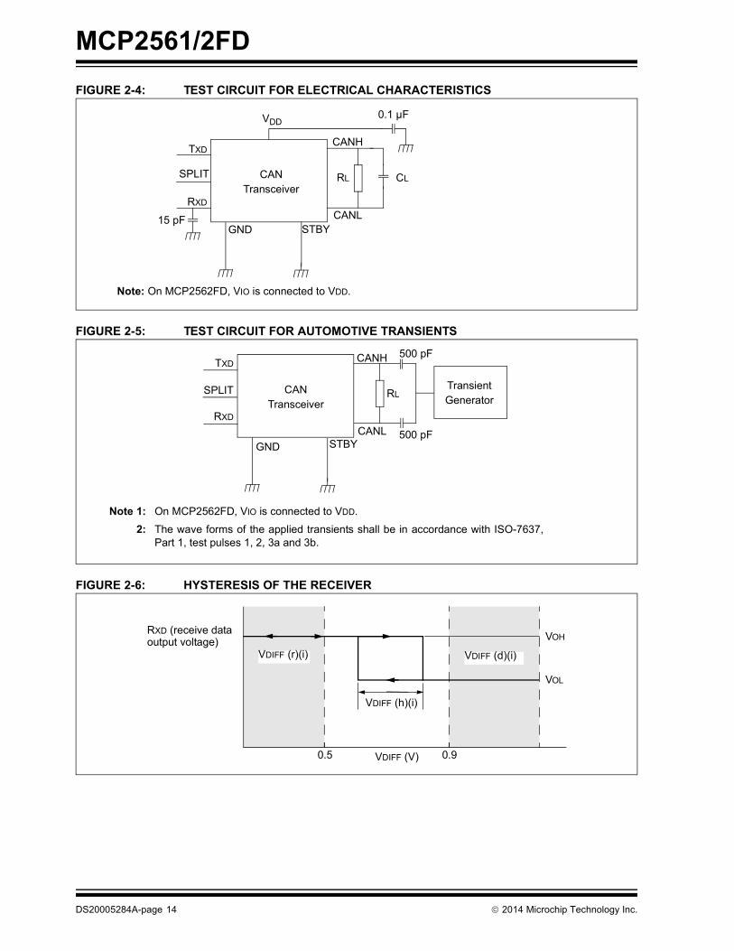
FIGURE 2-4: TEST CIRCUIT FOR ELECTRICAL CHARACTERISTICSFIGURE 2-5: TEST CIRCUIT FOR AUTOMOTIVE TRANSIENTS
FIGURE 2-6: HYSTERESIS OF THE RECEIVER
GND
RXD
SPLIT
TXD
RL CL
15 pF
CANH
CANL
CANTransceiver
0.1 µFVDD
STBY
Note: On MCP2562FD, VIO is connected to VDD.
GND
RXD
SPLIT
TXD
RL
500 pF
500 pF
Note 1: On MCP2562FD, VIO is connected to VDD.
2: The wave forms of the applied transients shall be in accordance with ISO-7637, Part 1, test pulses 1, 2, 3a and 3b.
CANH
CANL
CANTransceiver
TransientGenerator
STBY
VOH
VOL
0.5 0.9
VDIFF (h)(i)
VDIFF (V)
RXD (receive dataoutput voltage)
VDIFF (r)(i) VDIFF (d)(i)
DS20005284A-page 14 2014 Microchip Technology Inc.
MCP2561/2FD
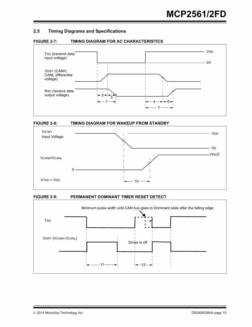
2.5 Timing Diagrams and SpecificationsFIGURE 2-7: TIMING DIAGRAM FOR AC CHARACTERISTICS
FIGURE 2-8: TIMING DIAGRAM FOR WAKEUP FROM STANDBY
FIGURE 2-9: PERMANENT DOMINANT TIMER RESET DETECT
3
7 47
0V
VDDTXD (transmit datainput voltage)
VDIFF (CANH,CANL differentialvoltage)
RXD (receive dataoutput voltage) 5
6
VTXD = VDD 10
0V
VDDVSTBY
VCANH/VCANL
Input Voltage
0
VDD/2
11 12
TXD
VDIFF (VCANH-VCANL)Driver is off
Minimum pulse width until CAN bus goes to Dominant state after the falling edge.
2014 Microchip Technology Inc. DS20005284A-page 15
MCP2561/2FD
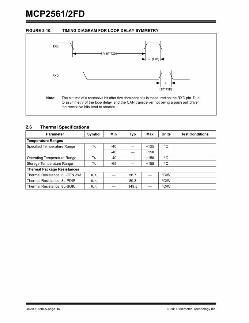
FIGURE 2-10: TIMING DIAGRAM FOR LOOP DELAY SYMMETRYTXD
5*tBIT(TXD)
tBIT(TXD)
tBIT(RXD)
RXD
8
Note: The bit time of a recessive bit after five dominant bits is measured on the RXD pin. Due to asymmetry of the loop delay, and the CAN transceiver not being a push pull driver, the recessive bits tend to shorten.
2.6 Thermal SpecificationsParameter Symbol Min Typ Max Units Test Conditions
Temperature RangesSpecified Temperature Range TA -40 — +125 C
-40 — +150Operating Temperature Range TA -40 — +150 CStorage Temperature Range TA -65 — +155 CThermal Package ResistancesThermal Resistance, 8L-DFN 3x3 JA — 56.7 — C/WThermal Resistance, 8L-PDIP JA — 89.3 — C/WThermal Resistance, 8L-SOIC JA — 149.5 — C/W
DS20005284A-page 16 2014 Microchip Technology Inc.
MCP2561/2FD
3.0 PACKAGING INFORMATION
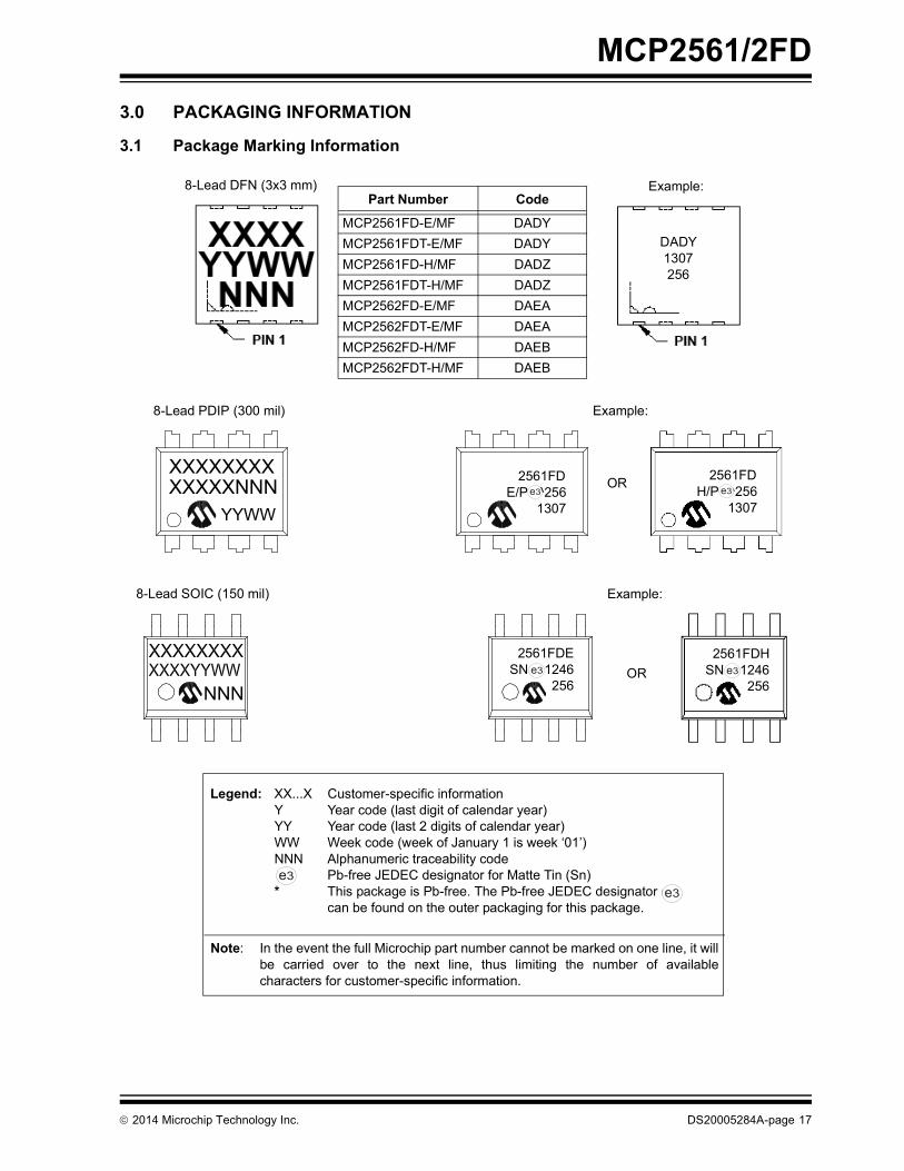
3.1 Package Marking Information
8-Lead PDIP (300 mil) Example:
8-Lead SOIC (150 mil) Example:
Legend: XX...X Customer-specific informationY Year code (last digit of calendar year)YY Year code (last 2 digits of calendar year)WW Week code (week of January 1 is week ‘01’)NNN Alphanumeric traceability code Pb-free JEDEC designator for Matte Tin (Sn)* This package is Pb-free. The Pb-free JEDEC designator ( )
can be found on the outer packaging for this package.
Note: In the event the full Microchip part number cannot be marked on one line, it will be carried over to the next line, thus limiting the number of available characters for customer-specific information.
3e
3e
Example:8-Lead DFN (3x3 mm)
8-Lead PDIP (300 mil) Example:
XXXXXXXXXXXXXNNN
YYWW
2561FDE/P ^^256
13073e
Part Number Code
MCP2561FD-E/MF DADYMCP2561FDT-E/MF DADYMCP2561FD-H/MF DADZMCP2561FDT-H/MF DADZMCP2562FD-E/MF DAEAMCP2562FDT-E/MF DAEAMCP2562FD-H/MF DAEBMCP2562FDT-H/MF DAEB
DADY1307256
NNN
2561FDE SN ^^1246
2563e OR
2561FDHSN ^^1246
2563e
OR 2561FDH/P ^^256
13073e
2014 Microchip Technology Inc. DS20005284A-page 17
MCP2561/2FD
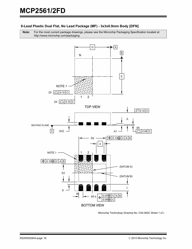
Note: For the most current package drawings, please see the Microchip Packaging Specification located at http://www.microchip.com/packaging
DS20005284A-page 18 2014 Microchip Technology Inc.
MCP2561/2FD
Note: For the most current package drawings, please see the Microchip Packaging Specification located at http://www.microchip.com/packaging
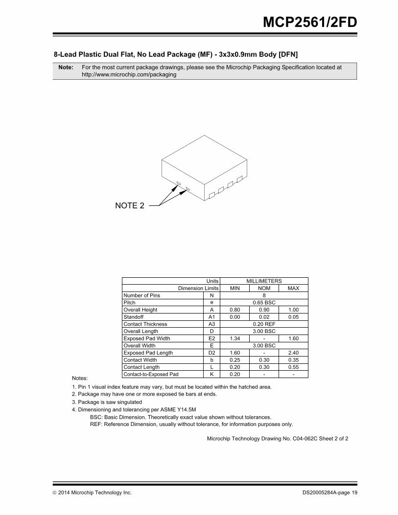
2014 Microchip Technology Inc. DS20005284A-page 19
MCP2561/2FD
Note: For the most current package drawings, please see the Microchip Packaging Specification located at http://www.microchip.com/packaging
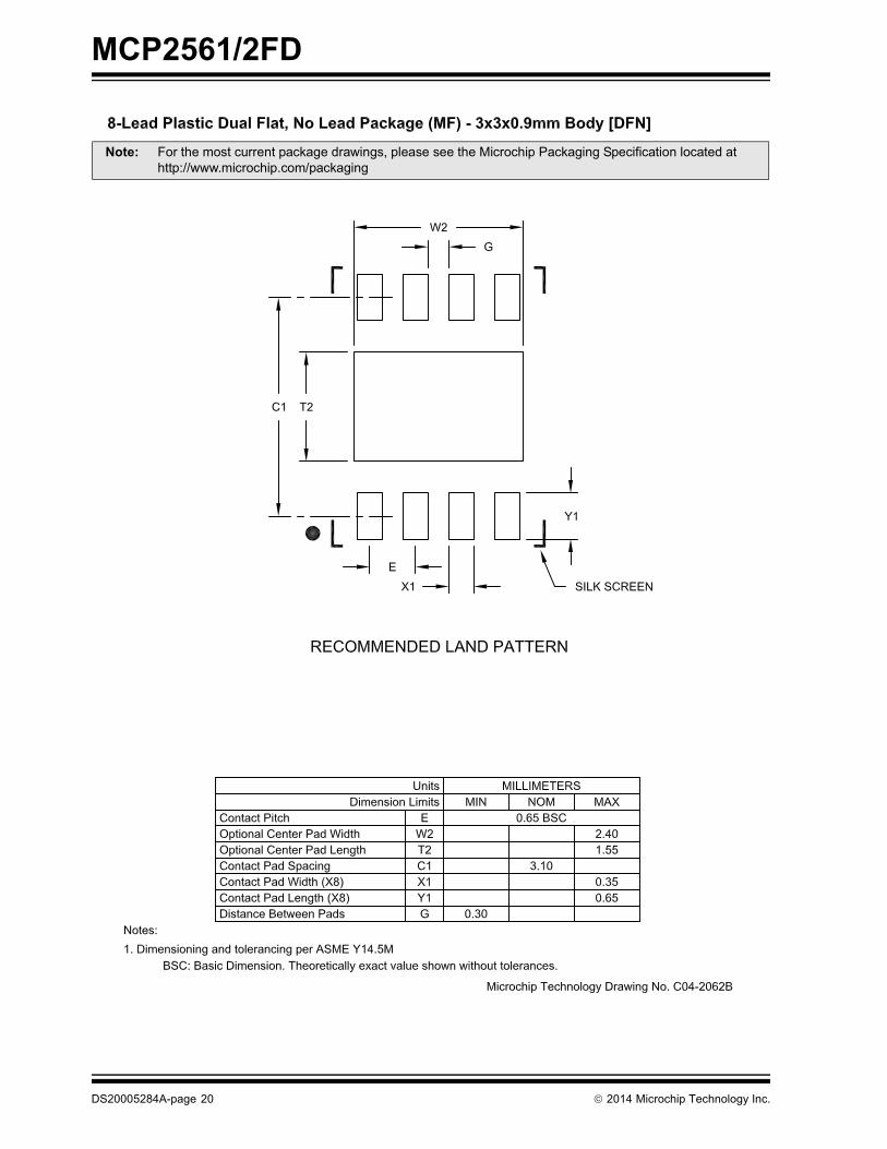
DS20005284A-page 20 2014 Microchip Technology Inc.
MCP2561/2FD
B
A
For the most current package drawings, please see the Microchip Packaging Specification located athttp://www.microchip.com/packaging
Note:
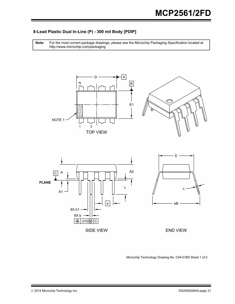
Microchip Technology Drawing No. C04-018D Sheet 1 of 2
8-Lead Plastic Dual In-Line (P) - 300 mil Body [PDIP]
eB
E
A
A1
A2
L
8X b
8X b1
D
E1
c
C
PLANE
.010 C
1 2
N
NOTE 1
TOP VIEW
END VIEWSIDE VIEW
e
2014 Microchip Technology Inc. DS20005284A-page 21
MCP2561/2FD
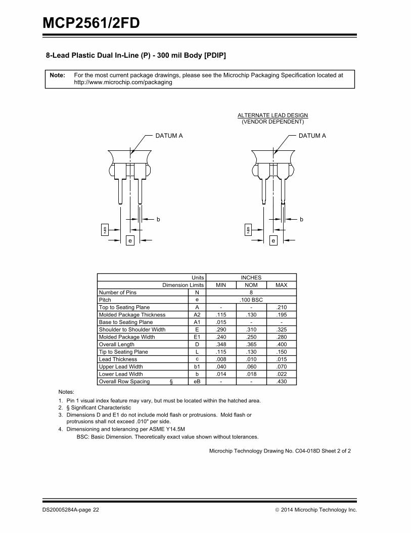
Microchip Technology Drawing No. C04-018D Sheet 2 of 2
For the most current package drawings, please see the Microchip Packaging Specification located athttp://www.microchip.com/packaging
Note:
8-Lead Plastic Dual In-Line (P) - 300 mil Body [PDIP]
Units INCHESDimension Limits MIN NOM MAX
Number of Pins N 8Pitch e .100 BSCTop to Seating Plane A - - .210Molded Package Thickness A2 .115 .130 .195Base to Seating Plane A1 .015Shoulder to Shoulder Width E .290 .310 .325Molded Package Width E1 .240 .250 .280Overall Length D .348 .365 .400Tip to Seating Plane L .115 .130 .150Lead Thickness c .008 .010 .015Upper Lead Width b1 .040 .060 .070Lower Lead Width b .014 .018 .022Overall Row Spacing eB - - .430
BSC: Basic Dimension. Theoretically exact value shown without tolerances.
3.
1.
protrusions shall not exceed .010" per side.
2.
4.
Notes:
§
- -
Dimensions D and E1 do not include mold flash or protrusions. Mold flash or
Pin 1 visual index feature may vary, but must be located within the hatched area.§ Significant Characteristic
Dimensioning and tolerancing per ASME Y14.5M
e
DATUM A DATUM A
e
be2
be2
ALTERNATE LEAD DESIGN(VENDOR DEPENDENT)
DS20005284A-page 22 2014 Microchip Technology Inc.
MCP2561/2FD
Note: For the most current package drawings, please see the Microchip Packaging Specification located at http://www.microchip.com/packaging
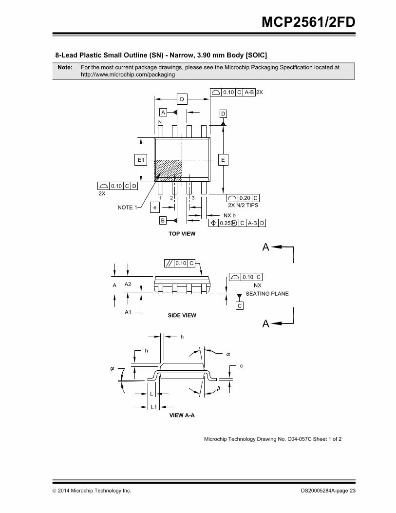
2014 Microchip Technology Inc. DS20005284A-page 23
MCP2561/2FD
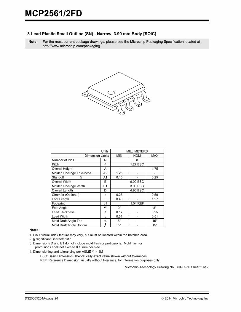
Note: For the most current package drawings, please see the Microchip Packaging Specification located at http://www.microchip.com/packaging
DS20005284A-page 24 2014 Microchip Technology Inc.
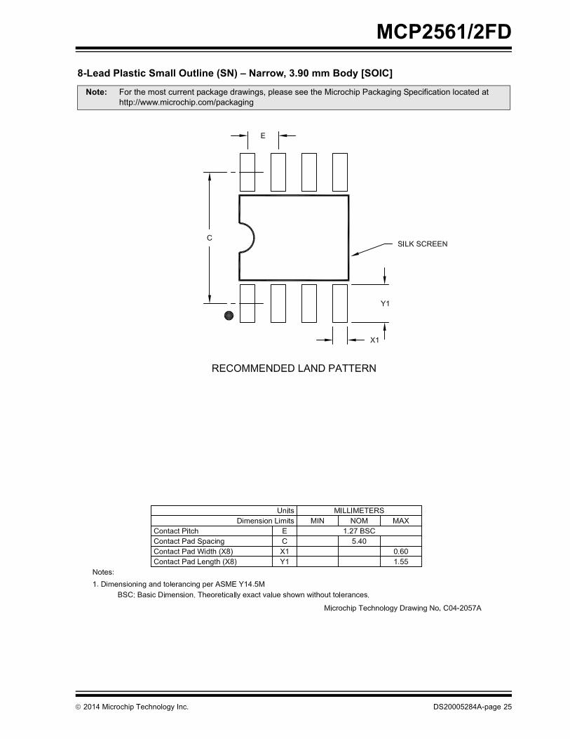
MCP2561/2FD
���������� ��������� �������������������������� ��!�"��#$%
����& ������!"���#�������$����%�&���"'�����"��"���������������(��$�����������)������������%��������*++&&&�!��������!+���$�����
2014 Microchip Technology Inc. DS20005284A-page 25

MCP2561/2FD
NOTES:DS20005284A-page 26 2014 Microchip Technology Inc.
MCP2561/2FD
APPENDIX A: REVISION HISTORY
Revision A (March 2014)Original Release of this Document.
2014 Microchip Technology Inc. DS20005284A-page 27
MCP2561/2FD
NOTES:DS20005284A-page 28 2014 Microchip Technology Inc.
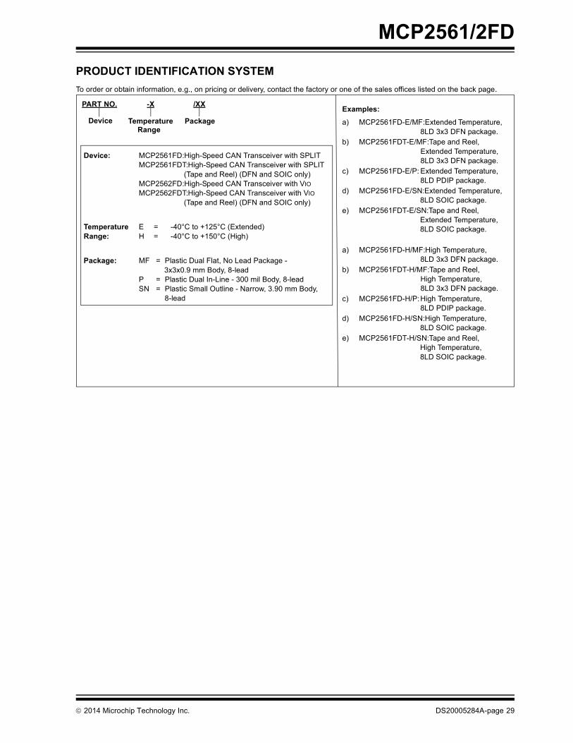
MCP2561/2FD
PRODUCT IDENTIFICATION SYSTEMTo order or obtain information, e.g., on pricing or delivery, contact the factory or one of the sales offices listed on the back page.
PART NO. -X /XX
PackageTemperatureRange
Device
Device: MCP2561FD:High-Speed CAN Transceiver with SPLITMCP2561FDT:High-Speed CAN Transceiver with SPLIT
(Tape and Reel) (DFN and SOIC only)MCP2562FD:High-Speed CAN Transceiver with VIOMCP2562FDT:High-Speed CAN Transceiver with VIO
(Tape and Reel) (DFN and SOIC only)
Temperature Range:
E = -40°C to +125°C (Extended)H = -40°C to +150°C (High)
Package: MF = Plastic Dual Flat, No Lead Package - 3x3x0.9 mm Body, 8-lead
P = Plastic Dual In-Line - 300 mil Body, 8-leadSN = Plastic Small Outline - Narrow, 3.90 mm Body,
8-lead
Examples:
a) MCP2561FD-E/MF:Extended Temperature,8LD 3x3 DFN package.
b) MCP2561FDT-E/MF:Tape and Reel,Extended Temperature,8LD 3x3 DFN package.
c) MCP2561FD-E/P: Extended Temperature,8LD PDIP package.
d) MCP2561FD-E/SN:Extended Temperature,8LD SOIC package.
e) MCP2561FDT-E/SN:Tape and Reel,Extended Temperature,8LD SOIC package.
a) MCP2561FD-H/MF:High Temperature,8LD 3x3 DFN package.
b) MCP2561FDT-H/MF:Tape and Reel,High Temperature,8LD 3x3 DFN package.
c) MCP2561FD-H/P:High Temperature,8LD PDIP package.
d) MCP2561FD-H/SN:High Temperature,8LD SOIC package.
e) MCP2561FDT-H/SN:Tape and Reel,High Temperature,8LD SOIC package.
2014 Microchip Technology Inc. DS20005284A-page 29

MCP2561/2FD
NOTES:DS20005284A-page 30 2014 Microchip Technology Inc.
Note the following details of the code protection feature on Microchip devices:• Microchip products meet the specification contained in their particular Microchip Data Sheet.
• Microchip believes that its family of products is one of the most secure families of its kind on the market today, when used in the intended manner and under normal conditions.
• There are dishonest and possibly illegal methods used to breach the code protection feature. All of these methods, to our knowledge, require using the Microchip products in a manner outside the operating specifications contained in Microchip’s Data Sheets. Most likely, the person doing so is engaged in theft of intellectual property.
• Microchip is willing to work with the customer who is concerned about the integrity of their code.
• Neither Microchip nor any other semiconductor manufacturer can guarantee the security of their code. Code protection does not mean that we are guaranteeing the product as “unbreakable.”
Code protection is constantly evolving. We at Microchip are committed to continuously improving the code protection features of our products. Attempts to break Microchip’s code protection feature may be a violation of the Digital Millennium Copyright Act. If such acts allow unauthorized access to your software or other copyrighted work, you may have a right to sue for relief under that Act.
Information contained in this publication regarding device applications and the like is provided only for your convenience and may be superseded by updates. It is your responsibility to ensure that your application meets with your specifications. MICROCHIP MAKES NO REPRESENTATIONS OR WARRANTIES OF ANY KIND WHETHER EXPRESS OR IMPLIED, WRITTEN OR ORAL, STATUTORY OR OTHERWISE, RELATED TO THE INFORMATION, INCLUDING BUT NOT LIMITED TO ITS CONDITION, QUALITY, PERFORMANCE, MERCHANTABILITY OR FITNESS FOR PURPOSE. Microchip disclaims all liability arising from this information and its use. Use of Microchip devices in life support and/or safety applications is entirely at the buyer’s risk, and the buyer agrees to defend, indemnify and hold harmless Microchip from any and all damages, claims, suits, or expenses resulting from such use. No licenses are conveyed, implicitly or otherwise, under any Microchip intellectual property rights.
2014 Microchip Technology Inc.
QUALITY MANAGEMENT SYSTEM CERTIFIED BY DNV
== ISO/TS 16949 ==
Trademarks
The Microchip name and logo, the Microchip logo, dsPIC, FlashFlex, KEELOQ, KEELOQ logo, MPLAB, PIC, PICmicro, PICSTART, PIC32 logo, rfPIC, SST, SST Logo, SuperFlash and UNI/O are registered trademarks of Microchip Technology Incorporated in the U.S.A. and other countries.
FilterLab, Hampshire, HI-TECH C, Linear Active Thermistor, MTP, SEEVAL and The Embedded Control Solutions Company are registered trademarks of Microchip Technology Incorporated in the U.S.A.
Silicon Storage Technology is a registered trademark of Microchip Technology Inc. in other countries.
Analog-for-the-Digital Age, Application Maestro, BodyCom, chipKIT, chipKIT logo, CodeGuard, dsPICDEM, dsPICDEM.net, dsPICworks, dsSPEAK, ECAN, ECONOMONITOR, FanSense, HI-TIDE, In-Circuit Serial Programming, ICSP, Mindi, MiWi, MPASM, MPF, MPLAB Certified logo, MPLIB, MPLINK, mTouch, Omniscient Code Generation, PICC, PICC-18, PICDEM, PICDEM.net, PICkit, PICtail, REAL ICE, rfLAB, Select Mode, SQI, Serial Quad I/O, Total Endurance, TSHARC, UniWinDriver, WiperLock, ZENA and Z-Scale are trademarks of Microchip Technology Incorporated in the U.S.A. and other countries.
SQTP is a service mark of Microchip Technology Incorporated in the U.S.A.
GestIC and ULPP are registered trademarks of Microchip Technology Germany II GmbH & Co. KG, a subsidiary of Microchip Technology Inc., in other countries.
All other trademarks mentioned herein are property of their respective companies.
© 2014, Microchip Technology Incorporated, Printed in the U.S.A., All Rights Reserved.
Printed on recycled paper.
ISBN: 978-1-63276-020-3
Microchip received ISO/TS-16949:2009 certification for its worldwide
DS20005284A-page 31
headquarters, design and wafer fabrication facilities in Chandler and Tempe, Arizona; Gresham, Oregon and design centers in California and India. The Company’s quality system processes and procedures are for its PIC® MCUs and dsPIC® DSCs, KEELOQ® code hopping devices, Serial EEPROMs, microperipherals, nonvolatile memory and analog products. In addition, Microchip’s quality system for the design and manufacture of development systems is ISO 9001:2000 certified.
DS20005284A-page 32 2014 Microchip Technology Inc.
AMERICASCorporate Office2355 West Chandler Blvd.Chandler, AZ 85224-6199Tel: 480-792-7200 Fax: 480-792-7277Technical Support: http://www.microchip.com/supportWeb Address: www.microchip.comAtlantaDuluth, GA Tel: 678-957-9614 Fax: 678-957-1455Austin, TXTel: 512-257-3370 BostonWestborough, MA Tel: 774-760-0087 Fax: 774-760-0088ChicagoItasca, IL Tel: 630-285-0071 Fax: 630-285-0075ClevelandIndependence, OH Tel: 216-447-0464 Fax: 216-447-0643DallasAddison, TX Tel: 972-818-7423 Fax: 972-818-2924DetroitNovi, MI Tel: 248-848-4000Houston, TX Tel: 281-894-5983IndianapolisNoblesville, IN Tel: 317-773-8323Fax: 317-773-5453Los AngelesMission Viejo, CA Tel: 949-462-9523 Fax: 949-462-9608New York, NY Tel: 631-435-6000San Jose, CA Tel: 408-735-9110Canada - TorontoTel: 905-673-0699 Fax: 905-673-6509
ASIA/PACIFICAsia Pacific OfficeSuites 3707-14, 37th FloorTower 6, The GatewayHarbour City, KowloonHong KongTel: 852-2943-5100Fax: 852-2401-3431Australia - SydneyTel: 61-2-9868-6733Fax: 61-2-9868-6755China - BeijingTel: 86-10-8569-7000 Fax: 86-10-8528-2104China - ChengduTel: 86-28-8665-5511Fax: 86-28-8665-7889China - ChongqingTel: 86-23-8980-9588Fax: 86-23-8980-9500China - HangzhouTel: 86-571-8792-8115 Fax: 86-571-8792-8116China - Hong Kong SARTel: 852-2943-5100 Fax: 852-2401-3431China - NanjingTel: 86-25-8473-2460Fax: 86-25-8473-2470China - QingdaoTel: 86-532-8502-7355Fax: 86-532-8502-7205China - ShanghaiTel: 86-21-5407-5533 Fax: 86-21-5407-5066China - ShenyangTel: 86-24-2334-2829Fax: 86-24-2334-2393China - ShenzhenTel: 86-755-8864-2200 Fax: 86-755-8203-1760China - WuhanTel: 86-27-5980-5300Fax: 86-27-5980-5118China - XianTel: 86-29-8833-7252Fax: 86-29-8833-7256China - XiamenTel: 86-592-2388138 Fax: 86-592-2388130China - ZhuhaiTel: 86-756-3210040 Fax: 86-756-3210049
ASIA/PACIFICIndia - BangaloreTel: 91-80-3090-4444 Fax: 91-80-3090-4123India - New DelhiTel: 91-11-4160-8631Fax: 91-11-4160-8632India - PuneTel: 91-20-3019-1500Japan - OsakaTel: 81-6-6152-7160 Fax: 81-6-6152-9310Japan - TokyoTel: 81-3-6880- 3770 Fax: 81-3-6880-3771Korea - DaeguTel: 82-53-744-4301Fax: 82-53-744-4302Korea - SeoulTel: 82-2-554-7200Fax: 82-2-558-5932 or 82-2-558-5934Malaysia - Kuala LumpurTel: 60-3-6201-9857Fax: 60-3-6201-9859Malaysia - PenangTel: 60-4-227-8870Fax: 60-4-227-4068Philippines - ManilaTel: 63-2-634-9065Fax: 63-2-634-9069SingaporeTel: 65-6334-8870Fax: 65-6334-8850Taiwan - Hsin ChuTel: 886-3-5778-366Fax: 886-3-5770-955Taiwan - KaohsiungTel: 886-7-213-7830Taiwan - TaipeiTel: 886-2-2508-8600 Fax: 886-2-2508-0102Thailand - BangkokTel: 66-2-694-1351Fax: 66-2-694-1350
EUROPEAustria - WelsTel: 43-7242-2244-39Fax: 43-7242-2244-393Denmark - CopenhagenTel: 45-4450-2828 Fax: 45-4485-2829France - ParisTel: 33-1-69-53-63-20 Fax: 33-1-69-30-90-79Germany - DusseldorfTel: 49-2129-3766400Germany - MunichTel: 49-89-627-144-0 Fax: 49-89-627-144-44Germany - PforzheimTel: 49-7231-424750Italy - Milan Tel: 39-0331-742611 Fax: 39-0331-466781Italy - VeniceTel: 39-049-7625286 Netherlands - DrunenTel: 31-416-690399 Fax: 31-416-690340Poland - WarsawTel: 48-22-3325737 Spain - MadridTel: 34-91-708-08-90Fax: 34-91-708-08-91Sweden - StockholmTel: 46-8-5090-4654UK - WokinghamTel: 44-118-921-5800Fax: 44-118-921-5820
Worldwide Sales and Service
03/25/14