Embed Size (px)
Citation preview
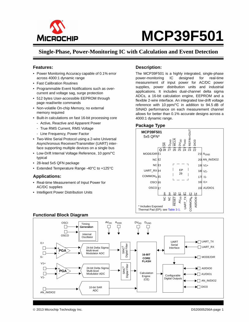
MCP39F501Single-Phase, Power-Monitoring IC with Calculation and Event Detection
Features:• Power Monitoring Accuracy capable of 0.1% error
across 4000:1 dynamic range
• Fast Calibration Routines
• Programmable Event Notifications such as over-current and voltage sag, surge protection
• 512 bytes User-accessible EEPROM through page read/write commands
• Non-volatile On-chip Memory, no external memory required
• Built-in calculations on fast 16-bit processing core
- Active, Reactive and Apparent Power
- True RMS Current, RMS Voltage
- Line Frequency, Power Factor
• Two-Wire Serial Protocol using a 2-wire Universal Asynchronous Receiver/Transmitter (UART) inter-face supporting multiple devices on a single bus
• Low-Drift Internal Voltage Reference, 10 ppm/°C typical
• 28-lead 5x5 QFN package
• Extended Temperature Range -40°C to +125°C
Applications:• Real-time Measurement of Input Power for
AC/DC supplies
• Intelligent Power Distribution Units
Description:The MCP39F501 is a highly integrated, single-phasepower-monitoring IC designed for real-timemeasurement of input power for AC/DC powersupplies, power distribution units and industrialapplications. It includes dual-channel delta sigmaADCs, a 16-bit calculation engine, EEPROM and aflexible 2-wire interface. An integrated low-drift voltagereference with 10 ppm/°C in addition to 94.5 dB ofSINAD performance on each measurement channelallows for better than 0.1% accurate designs across a4000:1 dynamic range.
Package Type
Functional Block Diagram
125
2
3
4
5
8 9 10 11 12
21
20
19
18
17
28 27 26 24MODE/DIR
NC
UART_RX
COMMONA
NCN
C
NC
AV
DD
UA
RT
_TX
RE
SE
T
DV
DD
DG
ND
MC
LR
EP29
6
7
OSCI
OSCO
13 14C
OM
MO
NB
A0/
DIO
0
16
15
23 22
RE
FIN
+/O
UT
DIO
3
I1+
I1-
V1-
V1+
AN_IN/DIO2
AGND
DG
ND
A1/DIO1
DR
MCP39F5015x5 QFN*
* Includes Exposed Thermal Pad (EP); see Table 3-1.
24-bit Delta Sigma Multi-level
+- S
INC
3
Dig
ital F
ilter
Modulator ADC PGA
I1+
I1-
24-bit Delta Sigma Multi-level
+- S
INC
3
Dig
ital F
ilter
Modulator ADC PGA
V1+
V1-
16-BITCORE
CalculationEngine
(CE)
ConfigurableDigital Outputs
UARTSerial
Interface
UART_TX
UART_RX
A0/DIO0
FLASH
10-bit SARADC
AN_IN/DIO2
OSCI
OSCO
Timing Generation
InternalOscillator
Generation
AVDD AGND DVDD DGND
A1/DIO1
MODE/DIR
DIO3
AN_IN/DIO2
2013 Microchip Technology Inc. DS20005256A-page 1
MCP39F501
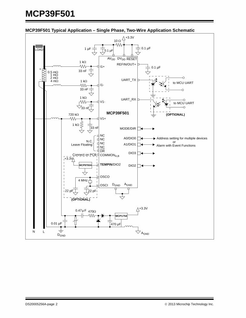
MCP39F501 Typical Application – Single Phase, Two-Wire Application Schematic
DGND
OSCO
OSCI
DVDD RESETAVDD
I1+
I1-
V1-
V1+
NCNCNC
REFIN/OUT+
AGND
COMMONA,B
NC
LOAD
+3.3V
N L
MCP1754
+3.3V
AGNDDGND
+
-
33 nF
33 nF
33 nF
1 k
1 k
1 k
720 k
1 k
4 MHz
22 pF 22 pF
33 nF
0.01 µF
0.47µ F 470
470 µF
10
1 µF0.1 µF
0.1 µF
0.1 µF
0.5 m1 m
TEMPIN/DIO2
2 m
Leave FloatingN.C.
MCP9700A
(OPTIONAL)
+3.3V
to MCU UART
to MCU UARTUART_RX
UART_TX
DR
(OPTIONAL)
Connect on PCB
A0/DIO0
DIO3
A1/DIO1
MODE/DIR
DIO2
Address setting for multiple devicesor
Alarm with Event Functions
MCP39F501
4 m
DS20005256A-page 2 2013 Microchip Technology Inc.
MCP39F501
1.0 ELECTRICAL CHARACTERISTICS
Absolute Maximum Ratings †
DVDD.....................................................................-0.3 to 4.5VAVDD .....................................................................-0.3 to 4.0VDigital inputs and outputs w.r.t. AGND................. -0.3V to 4.0VAnalog Inputs (I+,I-,V+,V-) w.r.t. AGND ............... ....-2V to +2VVREF input w.r.t. AGND .............................-0.6V to AVDD +0.6VMaximum Current out of DGND pin..............................300 mAMaximum Current into DVDD pin.................................250 mAMaximum Output Current Sunk by Digital IO................25 mAMaximum Current Sourced by Digital IO.......................25 mAStorage temperature .....................................-65°C to +150°CAmbient temperature with power applied......-40°C to +125°CSoldering temperature of leads (10 seconds) ............. +300°CESD on the analog inputs (HBM,MM).................4.0 kV, 200VESD on all other pins (HBM,MM)........................4.0 kV, 200V
† Notice: Stresses above those listed under “MaximumRatings” may cause permanent damage to the device.This is a stress rating only and functional operation ofthe device at those or any other conditions above thoseindicated in the operation listings of this specification isnot implied. Exposure to maximum rating conditions forextended periods may affect device reliability.
1.1 Specifications
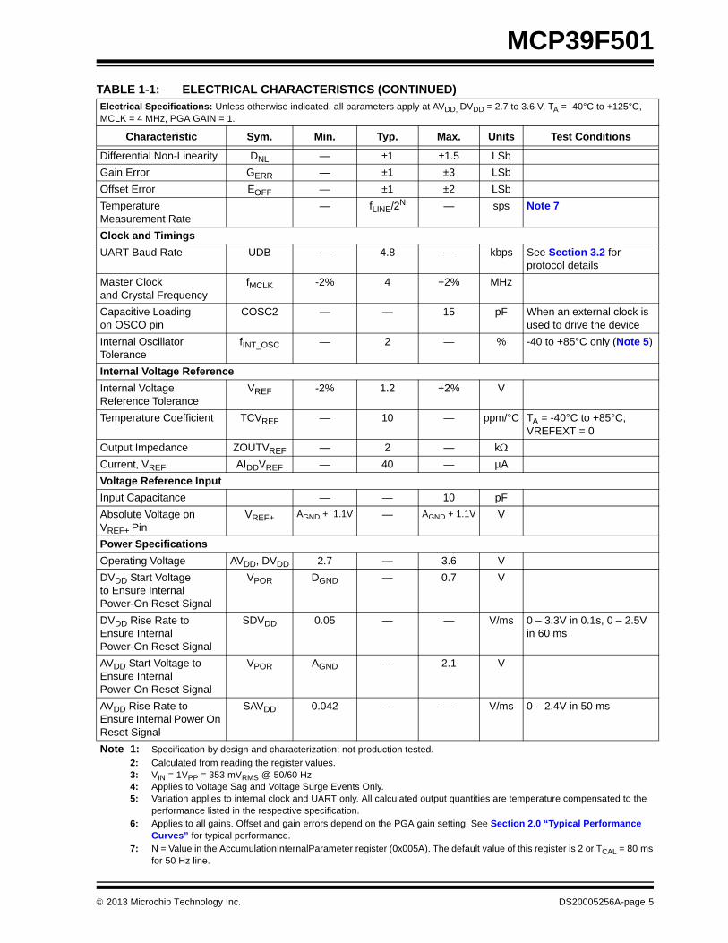
TABLE 1-1: ELECTRICAL CHARACTERISTICSElectrical Specifications: Unless otherwise indicated, all parameters apply at AVDD, DVDD = 2.7 to 3.6 V, TA = -40°C to +125°C, MCLK = 4 MHz, PGA GAIN = 1.
Characteristic Sym. Min. Typ. Max. Units Test Conditions
Power Measurement
Active Power (Note 2) P — ±0.1 — % 4000:1 Dynamic Range on Current Channel (Note 1)
Reactive Power (Note 2) Q — ±0.1 — % 4000:1 Dynamic Range on Current Channel (Note 1)
Apparent Power (Note 2) S — ±0.1 — % 4000:1 Dynamic Range on Current Channel (Note 1)
Current RMS (Note 2) IRMS — ±0.1 — % 4000:1 Dynamic Range on Current Channel (Note 1)
Voltage RMS (Note 2) VRMS — ±0.1 — % 4000:1 Dynamic Range on Voltage Channel (Note 1)
Power Factor (Note 2) — ±0.1 — %
Line Frequency (Note 2) VRMS — ±0.1 — %
Calibration, Calculation and Event Detection Times
Auto-Calibration Time tCAL — 2N x (1/fLINE) — ms Note 7
Minimum Calculationand Event Detection Time
tCALC_EVENT 2N x (1/fLINE) — — ms
Minimum Time for Voltage Sag Detection
tAC_DROP — see Section 7.7
— ms Note 4
Note 1: Specification by design and characterization; not production tested.
2: Calculated from reading the register values.3: VIN = 1VPP = 353 mVRMS @ 50/60 Hz.4: Applies to Voltage Sag and Voltage Surge Events Only.5: Variation applies to internal clock and UART only. All calculated output quantities are temperature compensated to the
performance listed in the respective specification.6: Applies to all gains. Offset and gain errors depend on the PGA gain setting. See Section 2.0 “Typical Performance
Curves” for typical performance.7: N = Value in the AccumulationInternalParameter register (0x005A). The default value of this register is 2 or TCAL = 80 ms
for 50 Hz line.
2013 Microchip Technology Inc. DS20005256A-page 3
MCP39F501
24-Bit Delta Sigma ADC Performance
Analog Input Absolute Voltage
VIN -1 — +1 V
Analog Input Leakage Current
AIN — 1 — nA
Differential Input Voltage Range
(I1+ – I1-),(V1+ – V1-)
-600/GAIN — +600/GAIN mV VREF = 1.2V, proportional to VREF
Offset Error VOS -1 — +1 mV
Offset Error Drift — 0.5 — µV/°C
Gain Error GE -4 — +4 % Note 6
Gain Error Drift — 1 — ppm/°C
Differential Input Impedance
ZIN 232 — — k G = 1
142 — — k G = 2
72 — — k G = 4
38 — — k G = 8
36 — — k G = 16
33 — — k G = 32
Signal-to-Noise and Distortion Ratio
SINAD 92 94.5 — dB Note 3
Total Harmonic Distortion THD — -106.5 -103 dBc Note 3
Signal-to-Noise Ratio SNR 92 95 — dB Note 3
Spurious Free Dynamic Range
SFDR — 111 — dB Note 3
Crosstalk CTALK — -122 — dB
AC Power Supply Rejection Ratio
AC PSRR — -73 — dB AVDD and DVDD = 3.3V + 0.6VPP, 100 Hz, 120 Hz, 1 kHz
DC Power Supply Rejection Ratio
DC PSRR — -73 — dB AVDD and DVDD = 3.0 to 3.6V
DC Common Mode Rejection Ratio
DC CMRR — -105 — dB VCM varies from -1V to +1V
10-Bit SAR ADC Performance for Temperature Measurement
Resolution NR — 10 — bits
Absolute Input Voltage VIN DGND - 0.3 — DGND + 0.3 V
Recommended Impedance of Analog Voltage Source
RIN — — 2.5 k
Integral Non-Linearity INL — ±1 ±2 LSb
TABLE 1-1: ELECTRICAL CHARACTERISTICS (CONTINUED)Electrical Specifications: Unless otherwise indicated, all parameters apply at AVDD, DVDD = 2.7 to 3.6 V, TA = -40°C to +125°C, MCLK = 4 MHz, PGA GAIN = 1.
Characteristic Sym. Min. Typ. Max. Units Test Conditions
Note 1: Specification by design and characterization; not production tested.
2: Calculated from reading the register values.3: VIN = 1VPP = 353 mVRMS @ 50/60 Hz.4: Applies to Voltage Sag and Voltage Surge Events Only.5: Variation applies to internal clock and UART only. All calculated output quantities are temperature compensated to the
performance listed in the respective specification.6: Applies to all gains. Offset and gain errors depend on the PGA gain setting. See Section 2.0 “Typical Performance
Curves” for typical performance.7: N = Value in the AccumulationInternalParameter register (0x005A). The default value of this register is 2 or TCAL = 80 ms
for 50 Hz line.
DS20005256A-page 4 2013 Microchip Technology Inc.
MCP39F501
Differential Non-Linearity DNL — ±1 ±1.5 LSb
Gain Error GERR — ±1 ±3 LSb
Offset Error EOFF — ±1 ±2 LSb
Temperature Measurement Rate
— fLINE/2N — sps Note 7
Clock and Timings
UART Baud Rate UDB — 4.8 — kbps See Section 3.2 for protocol details
Master Clock and Crystal Frequency
fMCLK -2% 4 +2% MHz
Capacitive Loading on OSCO pin
COSC2 — — 15 pF When an external clock is used to drive the device
Internal Oscillator Tolerance
fINT_OSC — 2 — % -40 to +85°C only (Note 5)
Internal Voltage Reference
Internal Voltage Reference Tolerance
VREF -2% 1.2 +2% V
Temperature Coefficient TCVREF — 10 — ppm/°C TA = -40°C to +85°C, VREFEXT = 0
Output Impedance ZOUTVREF — 2 — k
Current, VREF AIDDVREF — 40 — µA
Voltage Reference Input
Input Capacitance — — 10 pF
Absolute Voltage on VREF+ Pin
VREF+ AGND + 1.1V — AGND + 1.1V V
Power Specifications
Operating Voltage AVDD, DVDD 2.7 — 3.6 V
DVDD Start Voltage to Ensure Internal Power-On Reset Signal
VPOR DGND — 0.7 V
DVDD Rise Rate to Ensure Internal Power-On Reset Signal
SDVDD 0.05 — — V/ms 0 – 3.3V in 0.1s, 0 – 2.5V in 60 ms
AVDD Start Voltage to Ensure Internal Power-On Reset Signal
VPOR AGND — 2.1 V
AVDD Rise Rate to Ensure Internal Power On Reset Signal
SAVDD 0.042 — — V/ms 0 – 2.4V in 50 ms
TABLE 1-1: ELECTRICAL CHARACTERISTICS (CONTINUED)Electrical Specifications: Unless otherwise indicated, all parameters apply at AVDD, DVDD = 2.7 to 3.6 V, TA = -40°C to +125°C, MCLK = 4 MHz, PGA GAIN = 1.
Characteristic Sym. Min. Typ. Max. Units Test Conditions
Note 1: Specification by design and characterization; not production tested.
2: Calculated from reading the register values.3: VIN = 1VPP = 353 mVRMS @ 50/60 Hz.4: Applies to Voltage Sag and Voltage Surge Events Only.5: Variation applies to internal clock and UART only. All calculated output quantities are temperature compensated to the
performance listed in the respective specification.6: Applies to all gains. Offset and gain errors depend on the PGA gain setting. See Section 2.0 “Typical Performance
Curves” for typical performance.7: N = Value in the AccumulationInternalParameter register (0x005A). The default value of this register is 2 or TCAL = 80 ms
for 50 Hz line.
2013 Microchip Technology Inc. DS20005256A-page 5
MCP39F501
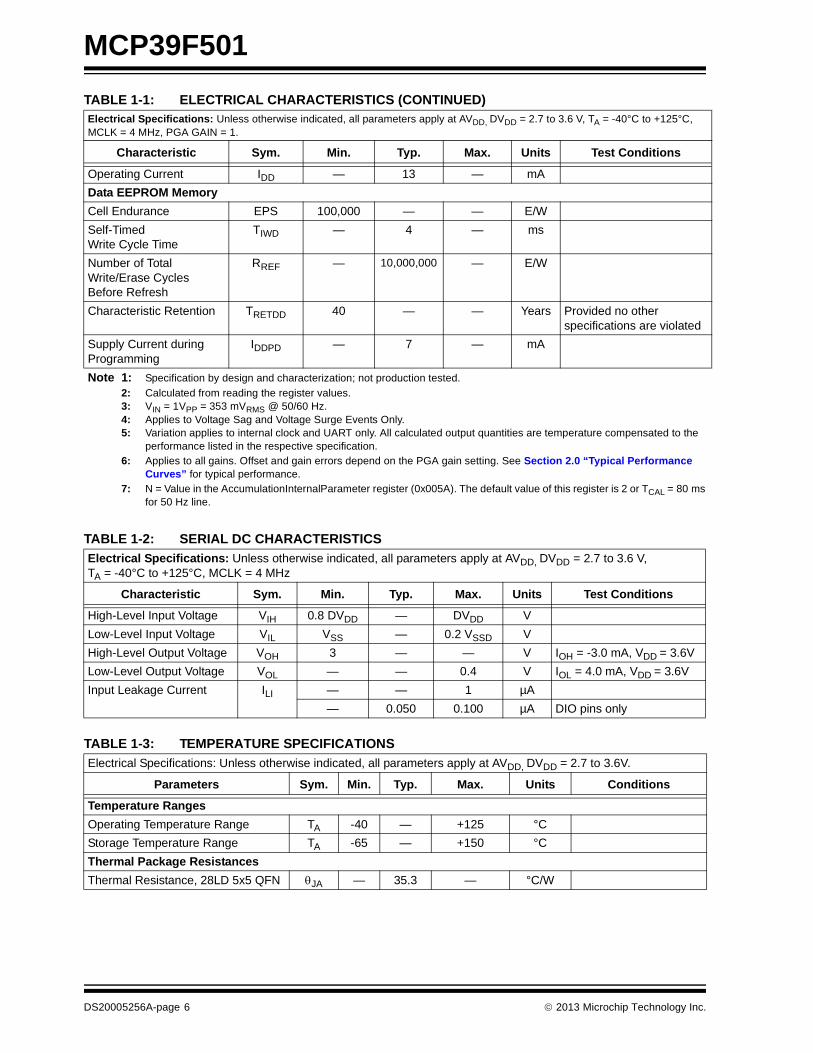
Operating Current IDD — 13 — mA
Data EEPROM Memory
Cell Endurance EPS 100,000 — — E/W
Self-Timed Write Cycle Time
TIWD — 4 — ms
Number of Total Write/Erase Cycles Before Refresh
RREF — 10,000,000 — E/W
Characteristic Retention TRETDD 40 — — Years Provided no other specifications are violated
Supply Current during Programming
IDDPD — 7 — mA
TABLE 1-2: SERIAL DC CHARACTERISTICS
Electrical Specifications: Unless otherwise indicated, all parameters apply at AVDD, DVDD = 2.7 to 3.6 V, TA = -40°C to +125°C, MCLK = 4 MHz
Characteristic Sym. Min. Typ. Max. Units Test Conditions
High-Level Input Voltage VIH 0.8 DVDD — DVDD V
Low-Level Input Voltage VIL VSS — 0.2 VSSD V
High-Level Output Voltage VOH 3 — — V IOH = -3.0 mA, VDD = 3.6V
Low-Level Output Voltage VOL — — 0.4 V IOL = 4.0 mA, VDD = 3.6V
Input Leakage Current ILI — — 1 µA
— 0.050 0.100 µA DIO pins only
TABLE 1-3: TEMPERATURE SPECIFICATIONS
Electrical Specifications: Unless otherwise indicated, all parameters apply at AVDD, DVDD = 2.7 to 3.6V.
Parameters Sym. Min. Typ. Max. Units Conditions
Temperature Ranges
Operating Temperature Range TA -40 — +125 °C
Storage Temperature Range TA -65 — +150 °C
Thermal Package Resistances
Thermal Resistance, 28LD 5x5 QFN JA — 35.3 — °C/W
TABLE 1-1: ELECTRICAL CHARACTERISTICS (CONTINUED)Electrical Specifications: Unless otherwise indicated, all parameters apply at AVDD, DVDD = 2.7 to 3.6 V, TA = -40°C to +125°C, MCLK = 4 MHz, PGA GAIN = 1.
Characteristic Sym. Min. Typ. Max. Units Test Conditions
Note 1: Specification by design and characterization; not production tested.
2: Calculated from reading the register values.3: VIN = 1VPP = 353 mVRMS @ 50/60 Hz.4: Applies to Voltage Sag and Voltage Surge Events Only.5: Variation applies to internal clock and UART only. All calculated output quantities are temperature compensated to the
performance listed in the respective specification.6: Applies to all gains. Offset and gain errors depend on the PGA gain setting. See Section 2.0 “Typical Performance
Curves” for typical performance.7: N = Value in the AccumulationInternalParameter register (0x005A). The default value of this register is 2 or TCAL = 80 ms
for 50 Hz line.
DS20005256A-page 6 2013 Microchip Technology Inc.
MCP39F501
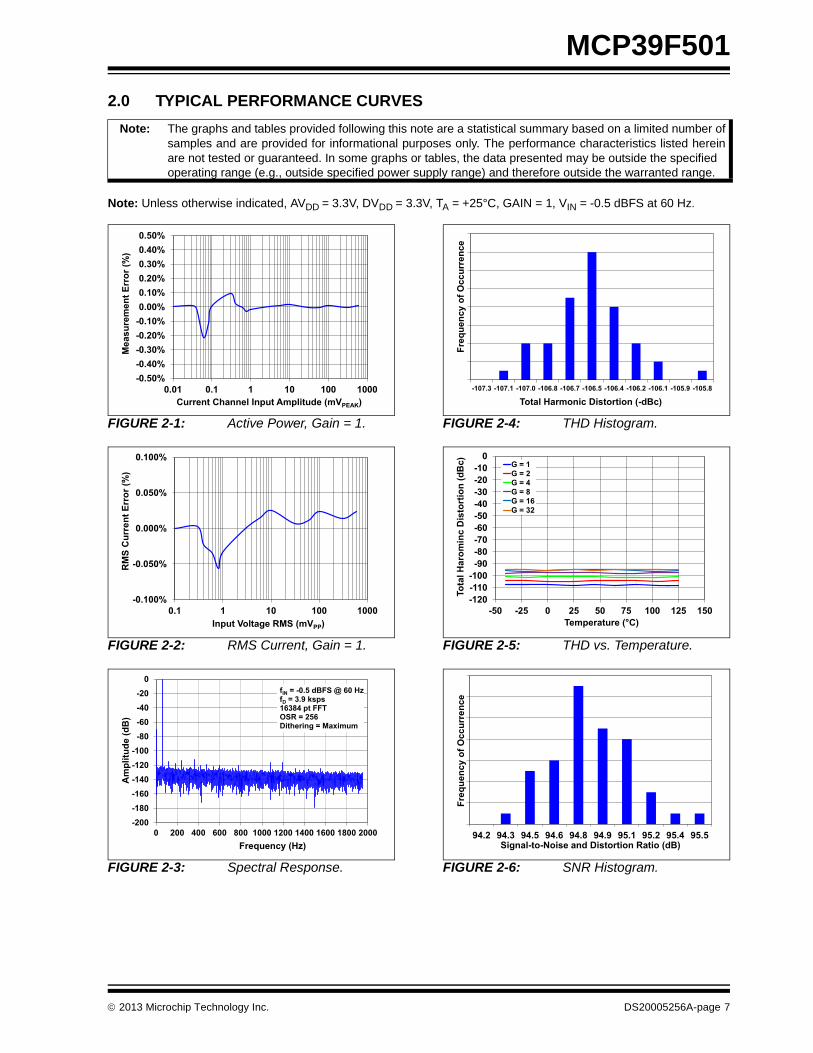
2.0 TYPICAL PERFORMANCE CURVES
Note: Unless otherwise indicated, AVDD = 3.3V, DVDD = 3.3V, TA = +25°C, GAIN = 1, VIN = -0.5 dBFS at 60 Hz.
FIGURE 2-1: Active Power, Gain = 1.
FIGURE 2-2: RMS Current, Gain = 1.
FIGURE 2-3: Spectral Response.
FIGURE 2-4: THD Histogram.
FIGURE 2-5: THD vs. Temperature.
FIGURE 2-6: SNR Histogram.
Note: The graphs and tables provided following this note are a statistical summary based on a limited number ofsamples and are provided for informational purposes only. The performance characteristics listed hereinare not tested or guaranteed. In some graphs or tables, the data presented may be outside the specifiedoperating range (e.g., outside specified power supply range) and therefore outside the warranted range.
-0.50%-0.40%-0.30%-0.20%-0.10%0.00%0.10%0.20%0.30%0.40%0.50%
0.01 0.1 1 10 100 1000
Mea
sure
men
t Err
or (%
)
Current Channel Input Amplitude (mVPEAK)
-0.100%
-0.050%
0.000%
0.050%
0.100%
0.1 1 10 100 1000
RM
S C
urre
nt E
rror
(%)
Input Voltage RMS (mVPP)
-200-180-160-140-120-100
-80-60-40-20
0
0 200 400 600 800 1000 1200 1400 1600 1800 2000
Am
plitu
de (d
B)
Frequency (Hz)
fIN = -0.5 dBFS @ 60 HzfD = 3.9 ksps16384 pt FFTOSR = 256Dithering = Maximum
-107.3 -107.1 -107.0 -106.8 -106.7 -106.5 -106.4 -106.2 -106.1 -105.9 -105.8
Freq
uenc
y of
Occ
urre
nce
Total Harmonic Distortion (-dBc)
-120-110-100-90-80-70-60-50-40-30-20-10
0
-50 -25 0 25 50 75 100 125 150
Tota
l Har
omin
c D
isto
rtio
n (d
Bc)
Temperature (°C)
G = 1G = 2G = 4G = 8G = 16G = 32
94.2 94.3 94.5 94.6 94.8 94.9 95.1 95.2 95.4 95.5
Freq
uenc
y of
Occ
urre
nce
Signal-to-Noise and Distortion Ratio (dB)
2013 Microchip Technology Inc. DS20005256A-page 7
MCP39F501
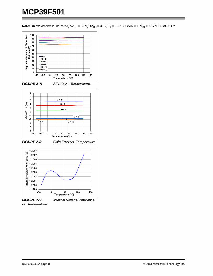
Note: Unless otherwise indicated, AVDD = 3.3V, DVDD = 3.3V, TA = +25°C, GAIN = 1, VIN = -0.5 dBFS at 60 Hz.
FIGURE 2-7: SINAD vs. Temperature.
FIGURE 2-8: Gain Error vs. Temperature.
FIGURE 2-9: Internal Voltage Reference vs. Temperature.
0102030405060708090
100
-50 -25 0 25 50 75 100 125 150
Sign
al-to
-Noi
se a
nd D
isto
rtio
n R
atio
n (d
B)
Temperature (°C)
G = 1G = 2G = 4G = 8G = 16G = 32
-5-4-3-2-1012345
-50 -25 0 25 50 75 100 125 150
Gai
n Er
ror (
%)
Temperature (°C)
G = 32 G = 16
G = 8
G = 4
G = 2
G = 1
1.1999
1.2000
1.2001
1.2002
1.2003
1.2004
1.2005
1.2006
1.2007
1.2008
-50 0 50 100 150
Inte
rnal
Vol
tage
Ref
eren
ce (V
)
Temperature (°C)
DS20005256A-page 8 2013 Microchip Technology Inc.
MCP39F501
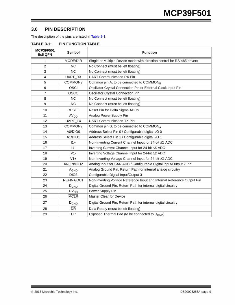
3.0 PIN DESCRIPTION
The description of the pins are listed in Table 3-1.
TABLE 3-1: PIN FUNCTION TABLE
MCP39F5015x5 QFN
Symbol Function
1 MODE/DIR Single or Multiple Device mode with direction control for RS-485 drivers
2 NC No Connect (must be left floating)
3 NC No Connect (must be left floating)
4 UART_RX UART Communication RX Pin
5 COMMONA Common pin A, to be connected to COMMONB
6 OSCI Oscillator Crystal Connection Pin or External Clock Input Pin
7 OSCO Oscillator Crystal Connection Pin
8 NC No Connect (must be left floating)
9 NC No Connect (must be left floating)
10 RESET Reset Pin for Delta Sigma ADCs
11 AVDD Analog Power Supply Pin
12 UART_TX UART Communication TX Pin
13 COMMONB Common pin B, to be connected to COMMONA
14 A0/DIO0 Address Select Pin 0 / Configurable digital I/O 0
15 A1/DIO1 Address Select Pin 1 / Configurable digital I/O 1
16 I1+ Non-Inverting Current Channel Input for 24-bit ADC
17 I1- Inverting Current Channel Input for 24-bit ADC
18 V1- Inverting Voltage Channel Input for 24-bit ADC
19 V1+ Non-Inverting Voltage Channel Input for 24-bit ADC
20 AN_IN/DIO2 Analog Input for SAR ADC / Configurable Digital Input/Output 2 Pin
21 AGND Analog Ground Pin, Return Path for internal analog circuitry
22 DIO3 Configurable Digital Input/Output 3
23 REFIN+/OUT Non-Inverting Voltage Reference Input and Internal Reference Output Pin
24 DGND Digital Ground Pin, Return Path for internal digital circuitry
25 DVDD Power Supply Pin
26 MCLR Master Clear for Device
27 DGND Digital Ground Pin, Return Path for internal digital circuitry
28 DR Data Ready (must be left floating)
29 EP Exposed Thermal Pad (to be connected to DGND)
2013 Microchip Technology Inc. DS20005256A-page 9
MCP39F501
3.1 Single/Multiple Device Mode and Direction Pin (MODE/DIR)
When using multiple devices on a single bus, this pinshould be tied to the DIR pin of the transceiver fordirection control. This will cause the A0/DIO0 andA1/DIO1 pins to act as address pins A0,A1. If additionaldevices are required, the Device Address register canbe programmed to allow for more than four devices.For this operation, a 4.7 k pull-down resistor shouldbe connected to this pin.
If only a single device is being used, the MODE pinshould be driven high at power-on reset (POR), makingthe A0/DIO0 and A1/DIO1 pins additional configurabledigital I/O (DIO).
3.2 UART Communication Pins (UART_TX, UART_RX)
The MCP39F501 device contains an asynchronousfull-duplex UART. The UART communication is 8 bitswith Start and Stop bit. See Section 4.2 “UARTSettings” for more information.
3.3 Common Pins (COMMON A and B)
The COMMONA and COMMONB pins are internalconnections for the MCP39F501. These two pinsshould be connected together in the application.
3.4 Data Ready Pin (DR)
The data ready pin indicates if a new delta-sigma A/Dconversion result is ready to be processed. This pin isfor indication only and should be left floating. After eachconversion is finished, a low pulse will take place on theData Ready pin to indicate the conversion result isready and an interrupt is generated in the calculationengine (CE). This pulse is synchronous with linefrequency and has a predefined and constant width.
3.5 Oscillator Pins (OSCO/OSCI)
OSCO and OSCI provide the master clock for thedevice. Appropriate load capacitance should beconnected to these pins for proper operation. Anoptional 4 MHz crystal can be connected to these pins.If a crystal of external clock source is not detected, thedevice will clock from the internal 4 MHz oscillator.
3.6 Reset Pin (RESET)
This pin is active-low and places the delta-sigmaADCs, PGA, internal VREF and other blocks associatedwith the analog front-end in a reset state when pulledlow. This input is Schmitt-triggered.
3.7 Analog Power Supply Pin (AVDD)
AVDD is the power supply pin for the analog circuitrywithin the MCP39F501.
This pin requires appropriate bypass capacitors andshould be maintained to 2.7V and 3.6V for specifiedoperation. It is recommended to use 0.1 µF ceramiccapacitors.
3.8 Digital Power Supply Pin (DVDD)
DVDD is the power supply pin for the digital circuitrywithin the MCP39F501. This pin requires appropriatebypass capacitors and should be maintained between2.7V and 3.6V for specified operation. It isrecommended to use 0.1 µF ceramic capacitors.
3.9 Configurable Digital Input/Output Pins (DIOn)
These digital I/O pins can be configured to act as inputor as output events, such as alarm events or interruptflags, based on the device configuration. For moreinformation, see Section 8.0 “Configurable DigitalI/O Pins (DIO Configuration – 0x0046)”.
3.10 24-Bit Delta Sigma ADC Differential Current Channel Input Pins (I1+/I1-)
I1- and I1+ are the two fully-differential current channelinputs for the Delta-Sigma ADCs.
The linear and specified region of the channels aredependent on the PGA gain. This region correspondsto a differential voltage range of ±600 mVPEAK/GAINwith VREF = 1.2V.
The maximum absolute voltage, with respect to AGND,for each In+/- input pin is ±1V with no distortion and±6V with no breaking after continuous voltage.
3.11 24-Bit Delta Sigma ADC Differential Voltage Channel Inputs (V1+/V1-)
V1- and V1+ are the two fully-differential voltagechannel inputs for the Delta-Sigma ADCs.
The linear and specified region of the channels aredependent on the PGA gain. This region correspondsto a differential voltage range of ±600 mVPEAK/GAINwith VREF = 1.2V.
The maximum absolute voltage, with respect to AGND,for each VN+/- input pin is ±1V with no distortion and±6V, with no breaking after continuous voltage.
Note: This pin is internally connected to the IRQof the calculation engine and should beleft floating.
DS20005256A-page 10 2013 Microchip Technology Inc.
MCP39F501
3.12 Analog Input for Temperature Measurement/Configurable Digital Output 2 Pin (AN_IN/DIO2)
This is the input to the analog-to-digital converter to beused for temperature measurement. If temperaturesensing is required in the application, it is advised toconnect the low-power active thermistorIC™ MCP9700A to this pin.
3.13 Analog Ground Pin (AGND)
AGND is the ground connection to internal analogcircuitry (ADCs, PGA, voltage reference, POR). If ananalog ground pin is available on the PCB, it isrecommended that this pin be tied to that plane.
3.14 Non-inverting Reference Input/Internal Reference Output Pin (REFIN+/OUT)
This pin is the non-inverting side of the differentialvoltage reference input for the delta sigma ADCs or theinternal voltage reference output.
For optimal performance, bypass capacitances shouldbe connected between this pin and AGND at all times,even when the internal voltage reference is used.However, these capacitors are not mandatory toensure proper operation.
3.15 Digital Ground Connection Pins (DGND)
DGND is the ground connection to internal digitalcircuitry (SINC filters, oscillator, serial interface). If adigital ground plane is available, it is recommended totie this pin to the digital plane of the PCB. This planeshould also reference all other digital circuitry in thesystem.
3.16 Exposed Thermal Pad (EP)
This pin is the exposed thermal pad. It must beconnected to DGND.
2013 Microchip Technology Inc. DS20005256A-page 11

MCP39F501
NOTES:
DS20005256A-page 12 2013 Microchip Technology Inc.
MCP39F501
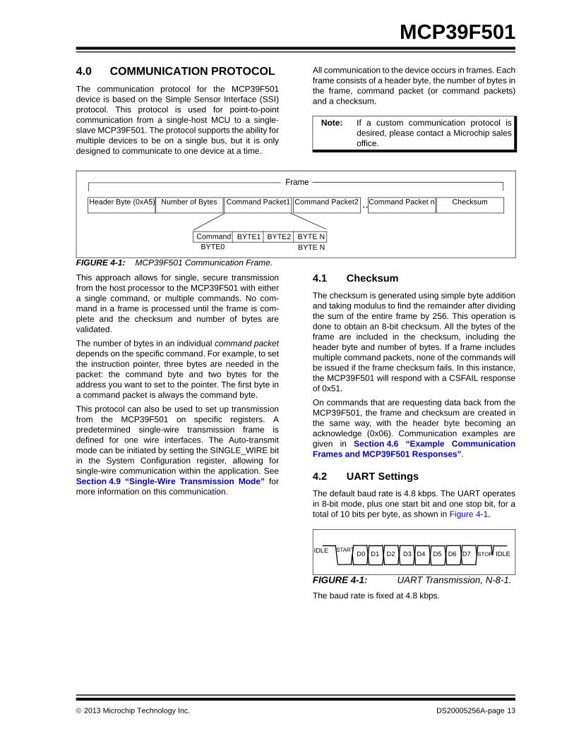
4.0 COMMUNICATION PROTOCOL
The communication protocol for the MCP39F501device is based on the Simple Sensor Interface (SSI)protocol. This protocol is used for point-to-pointcommunication from a single-host MCU to a single-slave MCP39F501. The protocol supports the ability formultiple devices to be on a single bus, but it is onlydesigned to communicate to one device at a time.
All communication to the device occurs in frames. Eachframe consists of a header byte, the number of bytes inthe frame, command packet (or command packets)and a checksum.
FIGURE 4-1: MCP39F501 Communication Frame.
This approach allows for single, secure transmissionfrom the host processor to the MCP39F501 with eithera single command, or multiple commands. No com-mand in a frame is processed until the frame is com-plete and the checksum and number of bytes arevalidated.
The number of bytes in an individual command packetdepends on the specific command. For example, to setthe instruction pointer, three bytes are needed in thepacket: the command byte and two bytes for theaddress you want to set to the pointer. The first byte ina command packet is always the command byte.
This protocol can also be used to set up transmissionfrom the MCP39F501 on specific registers. Apredetermined single-wire transmission frame isdefined for one wire interfaces. The Auto-transmitmode can be initiated by setting the SINGLE_WIRE bitin the System Configuration register, allowing forsingle-wire communication within the application. SeeSection 4.9 “Single-Wire Transmission Mode” formore information on this communication.
4.1 Checksum
The checksum is generated using simple byte additionand taking modulus to find the remainder after dividingthe sum of the entire frame by 256. This operation isdone to obtain an 8-bit checksum. All the bytes of theframe are included in the checksum, including theheader byte and number of bytes. If a frame includesmultiple command packets, none of the commands willbe issued if the frame checksum fails. In this instance,the MCP39F501 will respond with a CSFAIL responseof 0x51.
On commands that are requesting data back from theMCP39F501, the frame and checksum are created inthe same way, with the header byte becoming anacknowledge (0x06). Communication examples aregiven in Section 4.6 “Example CommunicationFrames and MCP39F501 Responses”.
4.2 UART Settings
The default baud rate is 4.8 kbps. The UART operatesin 8-bit mode, plus one start bit and one stop bit, for atotal of 10 bits per byte, as shown in Figure 4-1.
FIGURE 4-1: UART Transmission, N-8-1.
The baud rate is fixed at 4.8 kbps.
Note: If a custom communication protocol isdesired, please contact a Microchip salesoffice.
Header Byte (0xA5) Number of Bytes Command Packet1 Command Packet2 ...Command Packet n Checksum
Command BYTE0
BYTE1 BYTE2 BYTE N
BYTE N
Frame
IDLE STARTIDLESTOPD0 D1 D2 D3 D4 D5 D6 D7
2013 Microchip Technology Inc. DS20005256A-page 13
MCP39F501
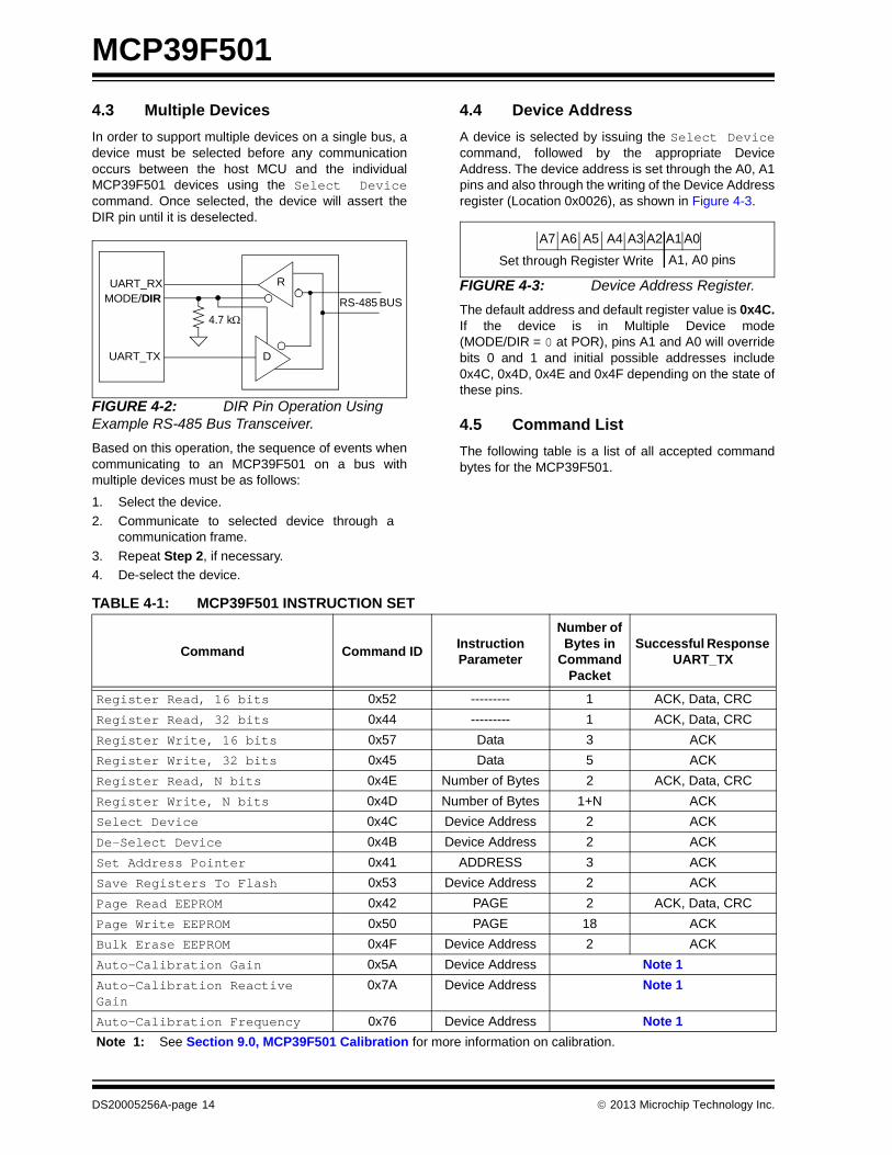
4.3 Multiple Devices
In order to support multiple devices on a single bus, adevice must be selected before any communicationoccurs between the host MCU and the individualMCP39F501 devices using the Select Devicecommand. Once selected, the device will assert theDIR pin until it is deselected.
FIGURE 4-2: DIR Pin Operation Using Example RS-485 Bus Transceiver.
Based on this operation, the sequence of events whencommunicating to an MCP39F501 on a bus withmultiple devices must be as follows:
1. Select the device.
2. Communicate to selected device through acommunication frame.
3. Repeat Step 2, if necessary.
4. De-select the device.
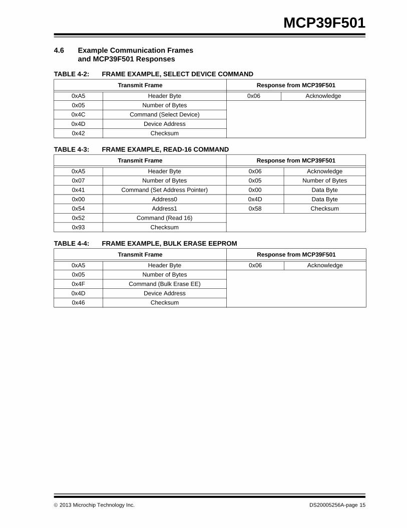
4.4 Device Address
A device is selected by issuing the Select Devicecommand, followed by the appropriate DeviceAddress. The device address is set through the A0, A1pins and also through the writing of the Device Addressregister (Location 0x0026), as shown in Figure 4-3.
FIGURE 4-3: Device Address Register.
The default address and default register value is 0x4C.If the device is in Multiple Device mode(MODE/DIR = 0 at POR), pins A1 and A0 will overridebits 0 and 1 and initial possible addresses include0x4C, 0x4D, 0x4E and 0x4F depending on the state ofthese pins.
4.5 Command List
The following table is a list of all accepted commandbytes for the MCP39F501.
R
D
4.7 k
UART_RXMODE/DIR
UART_TX
RS-485 BUS
A7 A6 A5 A4 A3 A2 A1 A0
Set through Register Write A1, A0 pins
TABLE 4-1: MCP39F501 INSTRUCTION SET
Command Command ID Instruction Parameter
Number of Bytes in
Command Packet
Successful Response UART_TX
Register Read, 16 bits 0x52 --------- 1 ACK, Data, CRC
Register Read, 32 bits 0x44 --------- 1 ACK, Data, CRC
Register Write, 16 bits 0x57 Data 3 ACK
Register Write, 32 bits 0x45 Data 5 ACK
Register Read, N bits 0x4E Number of Bytes 2 ACK, Data, CRC
Register Write, N bits 0x4D Number of Bytes 1+N ACK
Select Device 0x4C Device Address 2 ACK
De-Select Device 0x4B Device Address 2 ACK
Set Address Pointer 0x41 ADDRESS 3 ACK
Save Registers To Flash 0x53 Device Address 2 ACK
Page Read EEPROM 0x42 PAGE 2 ACK, Data, CRC
Page Write EEPROM 0x50 PAGE 18 ACK
Bulk Erase EEPROM 0x4F Device Address 2 ACK
Auto-Calibration Gain 0x5A Device Address Note 1
Auto-Calibration Reactive Gain
0x7A Device Address Note 1
Auto-Calibration Frequency 0x76 Device Address Note 1
Note 1: See Section 9.0, MCP39F501 Calibration for more information on calibration.
DS20005256A-page 14 2013 Microchip Technology Inc.
MCP39F501
4.6 Example Communication Frames and MCP39F501 Responses
TABLE 4-2: FRAME EXAMPLE, SELECT DEVICE COMMAND
Transmit Frame Response from MCP39F501
0xA5 Header Byte 0x06 Acknowledge
0x05 Number of Bytes
0x4C Command (Select Device)
0x4D Device Address
0x42 Checksum
TABLE 4-3: FRAME EXAMPLE, READ-16 COMMAND
Transmit Frame Response from MCP39F501
0xA5 Header Byte 0x06 Acknowledge
0x07 Number of Bytes 0x05 Number of Bytes
0x41 Command (Set Address Pointer) 0x00 Data Byte
0x00 Address0 0x4D Data Byte
0x54 Address1 0x58 Checksum
0x52 Command (Read 16)
0x93 Checksum
TABLE 4-4: FRAME EXAMPLE, BULK ERASE EEPROM
Transmit Frame Response from MCP39F501
0xA5 Header Byte 0x06 Acknowledge
0x05 Number of Bytes
0x4F Command (Bulk Erase EE)
0x4D Device Address
0x46 Checksum
2013 Microchip Technology Inc. DS20005256A-page 15
MCP39F501
4.7 Command Descriptions
4.7.1 REGISTER READ, 16-BIT (0X52)
The Register Read, 16-bit command, returns thetwo bytes that follow whatever the current addresspointer is set to. It should typically follow a SetAddress Pointer command. It can be used inconjunction with other read commands. Anacknowledge, data and checksum is the response forthis command. With this command the data is returnedMSB first.
4.7.2 REGISTER READ, 32-BIT (0X44)
The Register Read, 32-bit command, returns thefour bytes that follow whatever the current addresspointer is set to. It should typically follow a SetAddress Pointer command. It can be used inconjunction with other read commands. Anacknowledge, data and checksum is the response forthis command. With this command data is returnedMSB first.
4.7.3 REGISTER WRITE, 16-BIT (0X57)
The Register Write, 16-bit command isfollowed by bytes that will be written to whatever thecurrent address pointer is set to. It should typicallyfollow a Set Address Pointer command. It can beused in conjunction with other write commands. Anacknowledge is the response for this command.
4.7.4 REGISTER WRITE, 32-BIT (0X45)
The Register Write, 32-bit command isfollowed by four bytes that will be written to whateverthe current address pointer is set to. It should typicallyfollow a Set Address Pointer command. It can beused in conjunction with other write commands. Anacknowledge is the response for this command.
4.7.5 REGISTER READ, N BIT (0X4M)
The Register Read, N-bit command returns theN bytes that follow whatever the current addresspointer is set to. It should typically follow a SetAddress Pointer command. It can be used inconjunction with other read commands. Anacknowledge, data and checksum is the response forthis command. The maximum number of bytes that canbe read with this command is 48. If there are other readcommands within a frame, the maximum number ofbytes that can be read is 48 minus the number of bytesbeing read in the frame. With this command, the data isreturned LSB first.
4.7.6 REGISTER WRITE, N BIT (0X4D)
The Register Write, N-bit command is followedby N bytes that will be written to whatever the currentaddress pointer is set to. It should typically follow a SetAddress Pointer command. It can be used inconjunction with other write commands. Anacknowledge is the response for this command. Themaximum number of bytes that can be written with thiscommand is 64. If there are other write commandswithin a frame, the maximum number of bytes that canbe written is 64 minus the number of bytes beingwritten in the frame
4.7.7 SELECT DEVICE (0X4C)
The Select Device command is used to drive thedirection of the bus in Multiple Device mode byasserting the MODE/DIR pin. When the device is inSingle Device mode, this command has no effect onthe state of the pin. This command is expecting thedevice address as the command parameter, or thefollowing byte. The device address is a single bytelength. If the device address sent with this commandmatches the value in the MCP39F501’s DeviceAddress register, the pin will be asserted and anacknowledge returned.
4.7.8 DE-SELECT DEVICE (0X4B)
The Select Device command is used to drive thedirection of the bus by deasserting the MODE/DIR pin.When the device is in Single Device mode, thiscommand has no effect on the state of the pin. Thiscommand is expecting the Device Address as thecommand parameter, which is the following byte. TheDevice Address is a single byte length. If the deviceaddress sent with this command matches the value inthe MCP39F501’s Device Address register, the pin willbe deasserted and an acknowledge returned.
4.7.9 SET ADDRESS POINTER (0X41)
This command is used to set the address pointer for allread and write commands. This command is expectingthe address pointer as the command parameter in thefollowing two bytes. The address pointer is two bytesin length. If the address pointer is within the accept-able addresses of the device, an acknowledge will bereturned.
4.7.10 SAVE REGISTERS TO FLASH (0X53)
The Save Registers To Flash command makesa copy of all the calibration and configuration registersto flash. This includes all R/W registers in the registerset. This command is expecting the device address asthe instruction parameter, or the following byte. Thedevice address is a single byte length. If the deviceaddress matches, the response to this command is anacknowledge.
DS20005256A-page 16 2013 Microchip Technology Inc.
MCP39F501
4.7.11 PAGE READ EEPROM (0X42)
The Read Page EEPROM command returns 16 bytesof data that are stored in an individual page on theMCP39F501. A more complete description of the mem-ory organization of the EEPROM can be found inSection 10.0 “EEPROM”. This command is expectingthe EEPROM page as the command parameter or thefollowing byte. The response to this command is anacknowledge, 16-bytes of data and CRC checksum.
4.7.12 PAGE WRITE EEPROM (0X50)
The Write Page EEPROM command is expecting17 additional bytes in the command parameters, whichare EEPROM page plus 16 bytes of data. A morecomplete description of the memory organization of theEEPROM can be found in Section 10.0 “EEPROM”The response to this command is an acknowledge.
4.7.13 BULK ERASE EEPROM (0X4F)
The Bulk Erase EEPROM command will erase theentire EEPROM array and return it to a state of 0xFFFFfor each memory location of EEPROM. A morecomplete description of the memory organization of theEEPROM can be found in Section 10.0 “EEPROM”.This command is expecting the device address as thecommand parameter for additional security when bulkerasing the EEPROM of a device.
4.7.14 AUTO-CALIBRATION GAIN (0X5A)
The Auto-Calibration Gain command initiatesthe single point calibration that is all that is typicallyrequired for the system. This command calibrates theRMS current, RMS voltage and active power based onthe target values written in the corresponding registers.See Section 9.0 “MCP39F501 Calibration” for moreinformation on device calibration.
4.7.15 CALIBRATE FREQUENCY (0X76)
For applications not using an external crystal andrunning the MCP39F501 off the internal oscillator, again calibration to the line frequency indication isrequired. The Gain Line Frequency (0x00AE) registeris set such that the frequency indication matches whatis set in the Line Frequency Reference (0x0094)register. See Section 9.0 “MCP39F501 Calibration”for more information on device calibration.
4.8 Notation for Register Types
The following notation has been adopted for describingthe various registers used in the MCP39F501:
4.9 Single-Wire Transmission Mode
In Single-wire Transmission mode, at the end of eachcomputation cycle, the device automatically transmits aframe of power data. This allows for single-wire com-munication after the device has been configured.
The single-wire transmission frame consists of16 bytes: three Header Bytes, one Checksum and12 bytes of power data (including RMS current, RMSvoltage, Active Power and Line Frequency).
TABLE 4-5: SHORT-HAND NOTATION FOR REGISTER TYPES
Notation Description
u32 Unsigned, 32-bit register
s32 Signed, 32-bit register
u16 Unsigned, 16-bit register
s16 Signed, 16-bit register
b32 32-bit register containing discrete Boolean bit settings
TABLE 4-6: SINGLE-WIRE TRANSMISSION FRAME
# Byte
1 HEADERBYTE (0xAB)
2 HEADERBYTE2 (0xCD)
3 HEADERBYTE3 (0xEF)
4 CURRENT RMS – Byte 0
5 CURRENT RMS – Byte 1
6 CURRENT RMS – Byte 2
7 CURRENT RMS – Byte 3
8 VOLTAGE RMS – Byte 0
9 VOLTAGE RMS – Byte 1
10 ACTIVE POWER – Byte 0
11 ACTIVE POWER – Byte 1
12 ACTIVE POWER – Byte 2
13 ACTIVE POWER – Byte 3
14 LINE FREQUENCY – Byte 0
15 LINE FREQUENCY – Byte 1
16 CHECKSUM
Note 1: For custom single-wire transmission packets, contact a Microchip sales office.
2013 Microchip Technology Inc. DS20005256A-page 17

MCP39F501
NOTES:
DS20005256A-page 18 2013 Microchip Technology Inc.
MCP39F501
5.0 CALCULATION ENGINE (CE) DESCRIPTION
5.1 Computation Cycle Overview
The MCP39F501 uses a coherent sampling algorithmto lock the sampling rate to the line frequency, andreports all power output quantities at a 2N number ofline cycles. This is defined as a computation cycle andis dependent on the line frequency, so any change inthe line frequency will change the update rate of theoutput power quantities.
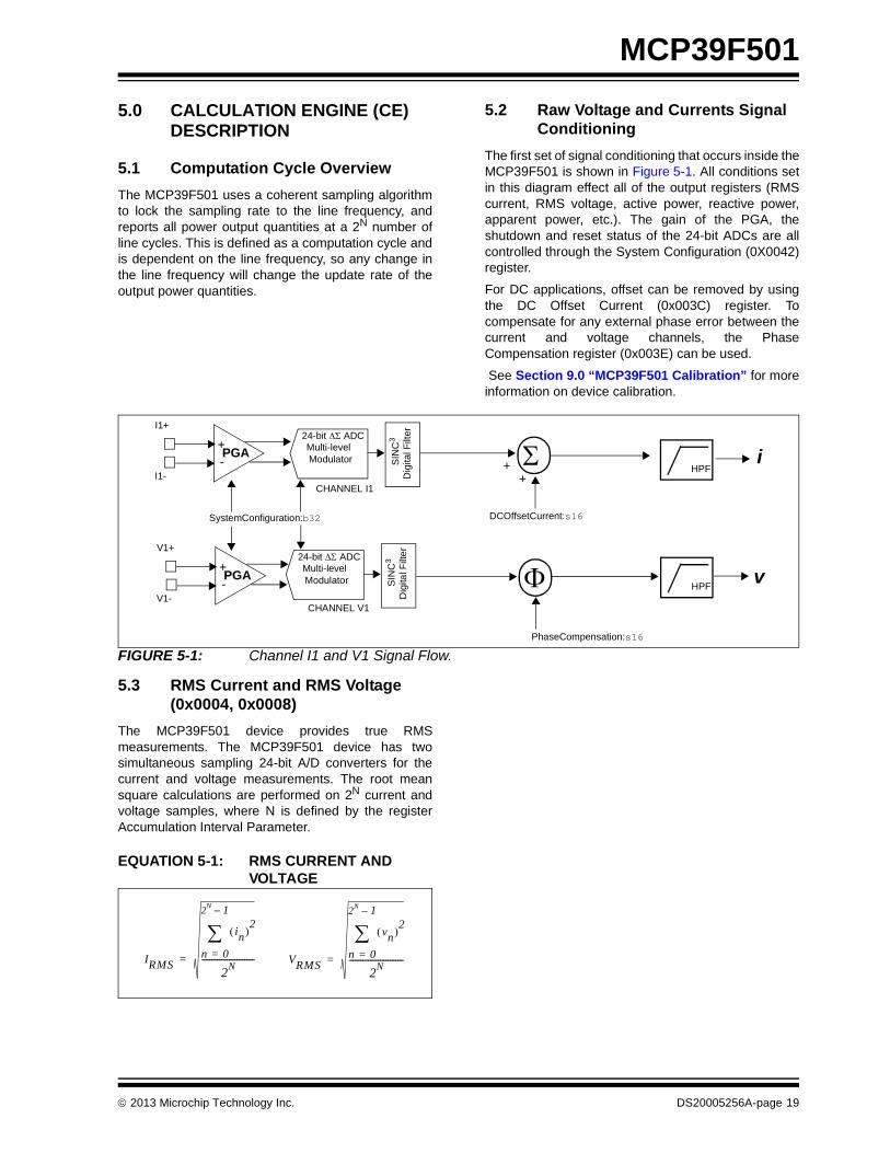
5.2 Raw Voltage and Currents Signal Conditioning
The first set of signal conditioning that occurs inside theMCP39F501 is shown in Figure 5-1. All conditions setin this diagram effect all of the output registers (RMScurrent, RMS voltage, active power, reactive power,apparent power, etc.). The gain of the PGA, theshutdown and reset status of the 24-bit ADCs are allcontrolled through the System Configuration (0X0042)register.
For DC applications, offset can be removed by usingthe DC Offset Current (0x003C) register. Tocompensate for any external phase error between thecurrent and voltage channels, the PhaseCompensation register (0x003E) can be used.
See Section 9.0 “MCP39F501 Calibration” for moreinformation on device calibration.
FIGURE 5-1: Channel I1 and V1 Signal Flow.
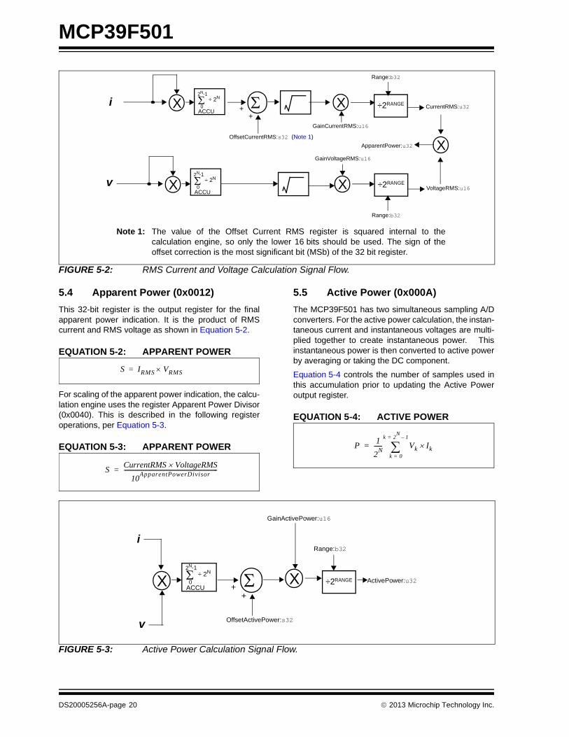
5.3 RMS Current and RMS Voltage (0x0004, 0x0008)
The MCP39F501 device provides true RMSmeasurements. The MCP39F501 device has twosimultaneous sampling 24-bit A/D converters for thecurrent and voltage measurements. The root meansquare calculations are performed on 2N current andvoltage samples, where N is defined by the registerAccumulation Interval Parameter.
EQUATION 5-1: RMS CURRENT AND VOLTAGE
CHANNEL I1
SIN
C3
Dig
ital F
ilter24-bit ADC
Multi-levelModulator
DCOffsetCurrent:s16
++
CHANNEL V1
SIN
C3
Dig
ital F
ilte
r
24-bit ADC Multi-levelModulator
HPF
PhaseCompensation:s16
HPF
+-PGA
I1+
I1-
+-PGA
V1+
V1-
SystemConfiguration:b32
i
v
IRMS
in 2
n 0=
2N 1–
2N
---------------------------= VRMS
vn 2
n 0=
2N 1–
2N
----------------------------=
2013 Microchip Technology Inc. DS20005256A-page 19
MCP39F501
FIGURE 5-2: RMS Current and Voltage Calculation Signal Flow.
5.4 Apparent Power (0x0012)
This 32-bit register is the output register for the finalapparent power indication. It is the product of RMScurrent and RMS voltage as shown in Equation 5-2.
EQUATION 5-2: APPARENT POWER
For scaling of the apparent power indication, the calcu-lation engine uses the register Apparent Power Divisor(0x0040). This is described in the following registeroperations, per Equation 5-3.
EQUATION 5-3: APPARENT POWER
5.5 Active Power (0x000A)
The MCP39F501 has two simultaneous sampling A/Dconverters. For the active power calculation, the instan-taneous current and instantaneous voltages are multi-plied together to create instantaneous power. Thisinstantaneous power is then converted to active powerby averaging or taking the DC component.
Equation 5-4 controls the number of samples used inthis accumulation prior to updating the Active Poweroutput register.
EQUATION 5-4: ACTIVE POWER
FIGURE 5-3: Active Power Calculation Signal Flow.
OffsetCurrentRMS:s32 (Note 1)
X CurrentRMS:u32++
Range:b32
X
÷2RANGE
VoltageRMS:u16
Range:b32
XApparentPower:u32
i
v
ACCU0
2N-1÷ 2N
ACCU0
2N-1÷ 2N
GainCurrentRMS:u16
X
X
GainVoltageRMS:u16
Note 1: The value of the Offset Current RMS register is squared internal to thecalculation engine, so only the lower 16 bits should be used. The sign of theoffset correction is the most significant bit (MSb) of the 32 bit register.
÷2RANGE
S IRMS VRMS=
SCurrentRMS VoltageRMS
10ApparentPowerDivisor
-------------------------------------------------------------------=
P1
2N
------ Vk Ikk 0=
k 2N
1–=
=
OffsetActivePower:s32
X ActivePower:u32+
+
X
GainActivePower:u16
Range:b32
ACCU0
2N-1÷ 2N
÷2RANGE
i
v
DS20005256A-page 20 2013 Microchip Technology Inc.
MCP39F501
5.6 Power Factor (0x0016)
Power factor is calculated by the ratio of P to S or activepower divided by apparent power.
EQUATION 5-5: POWER FACTOR
The Power Factor Reading is stored in a signed 16-bitregister (Power Factor, 0x0016). This register is asigned, 2's complement register with the MSBrepresenting the polarity of the power factor. Positivemeans inductive load, negative means capacitive load.Each LSB is then equivalent to a weight of 2-15. Amaximum register value of 0x7FFF corresponds to apower factor of 1. The minimum register value of0x8000 corresponds to a power factor of -1.
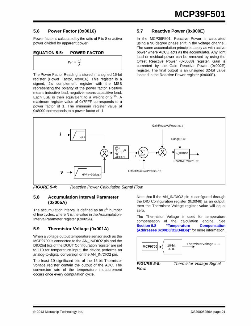
5.7 Reactive Power (0x000E)
In the MCP39F501, Reactive Power is calculatedusing a 90 degree phase shift in the voltage channel.The same accumulation principles apply as with activepower where ACCU acts as the accumulator. Any lightload or residual power can be removed by using theOffset Reactive Power (0x0038) register. Gain iscorrected by the Gain Reactive Power (0x002E)register. The final output is an unsigned 32-bit valuelocated in the Reactive Power register (0x000E).
FIGURE 5-4: Reactive Power Calculation Signal Flow.
5.8 Accumulation Interval Parameter (0x005A)
The accumulation interval is defined as an 2N numberof line cycles, where N is the value in the Accumulation-IntervalParameter register (0x005A).
5.9 Thermistor Voltage (0x001A)
When a voltage output temperature sensor such as theMCP9700 is connected to the AN_IN/DIO2 pin and theDIO2[n] bits of the DOUT Configuration register are setto 110 for temperature input, the device performs ananalog-to-digital conversion on the AN_IN/DIO2 pin.
The least 10 significant bits of the 16-bit ThermistorVoltage register contain the output of the ADC. Theconversion rate of the temperature measurementoccurs once every computation cycle.
Note that if the AN_IN/DIO2 pin is configured throughthe DIO Configuration register (0x0046) as an output,then the Thermistor Voltage register value will equalzero.
The Thermistor Voltage is used for temperaturecompensation of the calculation engine. SeeSection 9.8 “Temperature Compensation(Addresses 0x00B0/B2/B4/B6)” for more information.
FIGURE 5-5: Thermistor Voltage Signal Flow.
PFPS---=
OffsetReactivePower:s32
XACCU10
HPF
ReactivePower:u32
+-
HPF (+90deg.)
X
GainReactivePower:u16
Range:b32
2N-1÷ 2N ÷2RANGE
i
v
ThermistorVoltage:u1610-bit ADC
MCP9700
2013 Microchip Technology Inc. DS20005256A-page 21
MCP39F501
NOTES:
DS20005256A-page 22 2013 Microchip Technology Inc.
MCP39F501
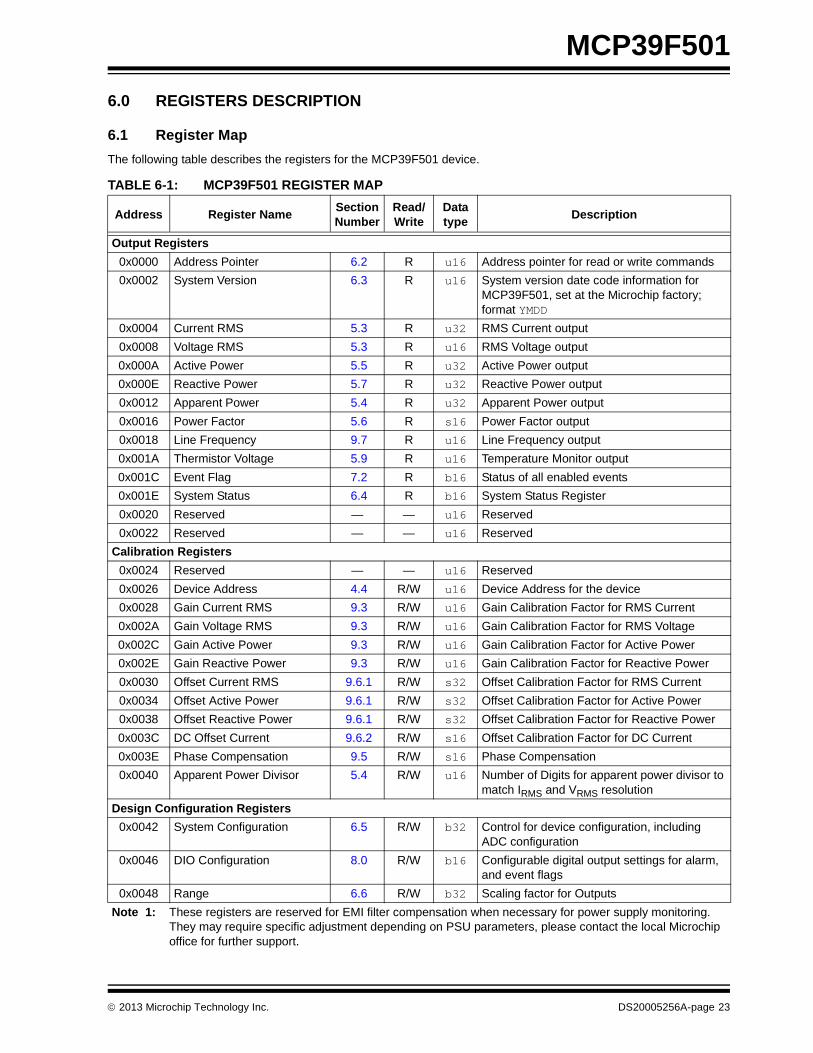
6.0 REGISTERS DESCRIPTION
6.1 Register Map
The following table describes the registers for the MCP39F501 device.
TABLE 6-1: MCP39F501 REGISTER MAP
Address Register NameSection Number
Read/Write
Data type
Description
Output Registers
0x0000 Address Pointer 6.2 R u16 Address pointer for read or write commands
0x0002 System Version 6.3 R u16 System version date code information for MCP39F501, set at the Microchip factory; format YMDD
0x0004 Current RMS 5.3 R u32 RMS Current output
0x0008 Voltage RMS 5.3 R u16 RMS Voltage output
0x000A Active Power 5.5 R u32 Active Power output
0x000E Reactive Power 5.7 R u32 Reactive Power output
0x0012 Apparent Power 5.4 R u32 Apparent Power output
0x0016 Power Factor 5.6 R s16 Power Factor output
0x0018 Line Frequency 9.7 R u16 Line Frequency output
0x001A Thermistor Voltage 5.9 R u16 Temperature Monitor output
0x001C Event Flag 7.2 R b16 Status of all enabled events
0x001E System Status 6.4 R b16 System Status Register
0x0020 Reserved — — u16 Reserved
0x0022 Reserved — — u16 Reserved
Calibration Registers
0x0024 Reserved — — u16 Reserved
0x0026 Device Address 4.4 R/W u16 Device Address for the device
0x0028 Gain Current RMS 9.3 R/W u16 Gain Calibration Factor for RMS Current
0x002A Gain Voltage RMS 9.3 R/W u16 Gain Calibration Factor for RMS Voltage
0x002C Gain Active Power 9.3 R/W u16 Gain Calibration Factor for Active Power
0x002E Gain Reactive Power 9.3 R/W u16 Gain Calibration Factor for Reactive Power
0x0030 Offset Current RMS 9.6.1 R/W s32 Offset Calibration Factor for RMS Current
0x0034 Offset Active Power 9.6.1 R/W s32 Offset Calibration Factor for Active Power
0x0038 Offset Reactive Power 9.6.1 R/W s32 Offset Calibration Factor for Reactive Power
0x003C DC Offset Current 9.6.2 R/W s16 Offset Calibration Factor for DC Current
0x003E Phase Compensation 9.5 R/W s16 Phase Compensation
0x0040 Apparent Power Divisor 5.4 R/W u16 Number of Digits for apparent power divisor to match IRMS and VRMS resolution
Design Configuration Registers
0x0042 System Configuration 6.5 R/W b32 Control for device configuration, including ADC configuration
0x0046 DIO Configuration 8.0 R/W b16 Configurable digital output settings for alarm, and event flags
0x0048 Range 6.6 R/W b32 Scaling factor for Outputs
Note 1: These registers are reserved for EMI filter compensation when necessary for power supply monitoring. They may require specific adjustment depending on PSU parameters, please contact the local Microchip office for further support.
2013 Microchip Technology Inc. DS20005256A-page 23
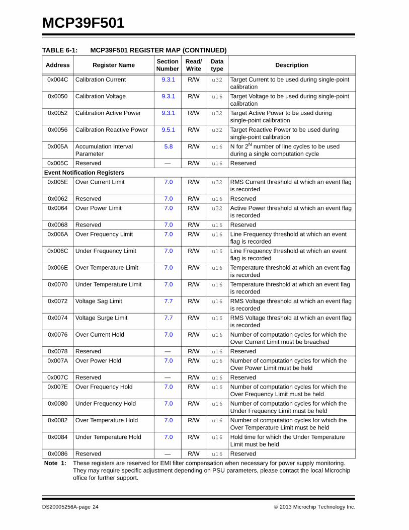
MCP39F501
0x004C Calibration Current 9.3.1 R/W u32 Target Current to be used during single-point calibration
0x0050 Calibration Voltage 9.3.1 R/W u16 Target Voltage to be used during single-point calibration
0x0052 Calibration Active Power 9.3.1 R/W u32 Target Active Power to be used during single-point calibration
0x0056 Calibration Reactive Power 9.5.1 R/W u32 Target Reactive Power to be used during single-point calibration
0x005A Accumulation Interval Parameter
5.8 R/W u16 N for 2N number of line cycles to be used during a single computation cycle
0x005C Reserved — R/W u16 Reserved
Event Notification Registers
0x005E Over Current Limit 7.0 R/W u32 RMS Current threshold at which an event flag is recorded
0x0062 Reserved 7.0 R/W u16 Reserved
0x0064 Over Power Limit 7.0 R/W u32 Active Power threshold at which an event flag is recorded
0x0068 Reserved 7.0 R/W u16 Reserved
0x006A Over Frequency Limit 7.0 R/W u16 Line Frequency threshold at which an event flag is recorded
0x006C Under Frequency Limit 7.0 R/W u16 Line Frequency threshold at which an event flag is recorded
0x006E Over Temperature Limit 7.0 R/W u16 Temperature threshold at which an event flag is recorded
0x0070 Under Temperature Limit 7.0 R/W u16 Temperature threshold at which an event flag is recorded
0x0072 Voltage Sag Limit 7.7 R/W u16 RMS Voltage threshold at which an event flag is recorded
0x0074 Voltage Surge Limit 7.7 R/W u16 RMS Voltage threshold at which an event flag is recorded
0x0076 Over Current Hold 7.0 R/W u16 Number of computation cycles for which the Over Current Limit must be breached
0x0078 Reserved — R/W u16 Reserved
0x007A Over Power Hold 7.0 R/W u16 Number of computation cycles for which the Over Power Limit must be held
0x007C Reserved — R/W u16 Reserved
0x007E Over Frequency Hold 7.0 R/W u16 Number of computation cycles for which the Over Frequency Limit must be held
0x0080 Under Frequency Hold 7.0 R/W u16 Number of computation cycles for which the Under Frequency Limit must be held
0x0082 Over Temperature Hold 7.0 R/W u16 Number of computation cycles for which the Over Temperature Limit must be held
0x0084 Under Temperature Hold 7.0 R/W u16 Hold time for which the Under Temperature Limit must be held
0x0086 Reserved — R/W u16 Reserved
TABLE 6-1: MCP39F501 REGISTER MAP (CONTINUED)
Address Register NameSection Number
Read/Write
Data type
Description
Note 1: These registers are reserved for EMI filter compensation when necessary for power supply monitoring. They may require specific adjustment depending on PSU parameters, please contact the local Microchip office for further support.
DS20005256A-page 24 2013 Microchip Technology Inc.
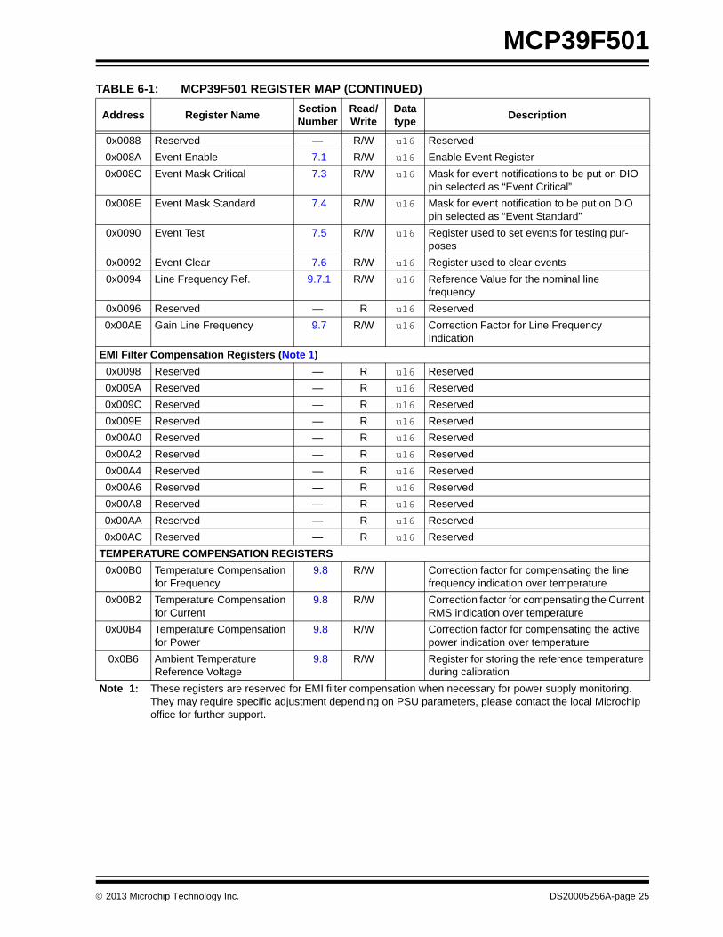
MCP39F501
0x0088 Reserved — R/W u16 Reserved
0x008A Event Enable 7.1 R/W u16 Enable Event Register
0x008C Event Mask Critical 7.3 R/W u16 Mask for event notifications to be put on DIO pin selected as “Event Critical”
0x008E Event Mask Standard 7.4 R/W u16 Mask for event notification to be put on DIO pin selected as “Event Standard”
0x0090 Event Test 7.5 R/W u16 Register used to set events for testing pur-poses
0x0092 Event Clear 7.6 R/W u16 Register used to clear events
0x0094 Line Frequency Ref. 9.7.1 R/W u16 Reference Value for the nominal line frequency
0x0096 Reserved — R u16 Reserved
0x00AE Gain Line Frequency 9.7 R/W u16 Correction Factor for Line Frequency Indication
EMI Filter Compensation Registers (Note 1)
0x0098 Reserved — R u16 Reserved
0x009A Reserved — R u16 Reserved
0x009C Reserved — R u16 Reserved
0x009E Reserved — R u16 Reserved
0x00A0 Reserved — R u16 Reserved
0x00A2 Reserved — R u16 Reserved
0x00A4 Reserved — R u16 Reserved
0x00A6 Reserved — R u16 Reserved
0x00A8 Reserved — R u16 Reserved
0x00AA Reserved — R u16 Reserved
0x00AC Reserved — R u16 Reserved
TEMPERATURE COMPENSATION REGISTERS
0x00B0 Temperature Compensation for Frequency
9.8 R/W Correction factor for compensating the line frequency indication over temperature
0x00B2 Temperature Compensation for Current
9.8 R/W Correction factor for compensating the Current RMS indication over temperature
0x00B4 Temperature Compensation for Power
9.8 R/W Correction factor for compensating the active power indication over temperature
0x0B6 Ambient Temperature Reference Voltage
9.8 R/W Register for storing the reference temperature during calibration
TABLE 6-1: MCP39F501 REGISTER MAP (CONTINUED)
Address Register NameSection Number
Read/Write
Data type
Description
Note 1: These registers are reserved for EMI filter compensation when necessary for power supply monitoring. They may require specific adjustment depending on PSU parameters, please contact the local Microchip office for further support.
2013 Microchip Technology Inc. DS20005256A-page 25
MCP39F501
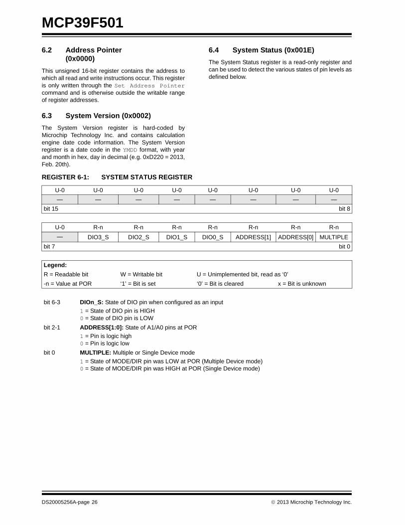
6.2 Address Pointer (0x0000)
This unsigned 16-bit register contains the address towhich all read and write instructions occur. This registeris only written through the Set Address Pointercommand and is otherwise outside the writable rangeof register addresses.
6.3 System Version (0x0002)
The System Version register is hard-coded byMicrochip Technology Inc. and contains calculationengine date code information. The System Versionregister is a date code in the YMDD format, with yearand month in hex, day in decimal (e.g. 0xD220 = 2013,Feb. 20th).
6.4 System Status (0x001E)
The System Status register is a read-only register andcan be used to detect the various states of pin levels asdefined below.
REGISTER 6-1: SYSTEM STATUS REGISTER
U-0 U-0 U-0 U-0 U-0 U-0 U-0 U-0
— — — — — — — —
bit 15 bit 8
U-0 R-n R-n R-n R-n R-n R-n R-n
— DIO3_S DIO2_S DIO1_S DIO0_S ADDRESS[1] ADDRESS[0] MULTIPLE
bit 7 bit 0
Legend:
R = Readable bit W = Writable bit U = Unimplemented bit, read as ‘0’
-n = Value at POR ‘1’ = Bit is set ‘0’ = Bit is cleared x = Bit is unknown
bit 6-3 DIOn_S: State of DIO pin when configured as an input
1 = State of DIO pin is HIGH0 = State of DIO pin is LOW
bit 2-1 ADDRESS[1:0]: State of A1/A0 pins at POR
1 = Pin is logic high0 = Pin is logic low
bit 0 MULTIPLE: Multiple or Single Device mode
1 = State of MODE/DIR pin was LOW at POR (Multiple Device mode)0 = State of MODE/DIR pin was HIGH at POR (Single Device mode)
DS20005256A-page 26 2013 Microchip Technology Inc.
MCP39F501
6.5 System Configuration (0x0042)
The System Configuration register contains bits for thefollowing control:
• PGA setting
• ADC Reset State
• ADC Shutdown State
• Voltage Reference Trim
• Single Wire Auto-transmission
These options are described in the following sections.
6.5.1 PROGRAMMABLE GAIN AMPLIFIERS (PGA)
The two Programmable Gain Amplifiers (PGAs) resideat the front-end of each 24-bit Delta-Sigma ADC. Theyhave two functions:
• Translate the common-mode of the input from AGND to an internal level between AGND and AVDD
• Amplify the input differential signal
The translation of the common mode does not changethe differential signal but recenters the common-modeso that the input signal can be properly amplified.
The PGA block can be used to amplify very low signals,but the differential input range of the delta-sigmamodulator must not be exceeded. The PGA iscontrolled by the PGA_CHn<2:0> bits in Register 6-2the System Configuration register. Table 6-2 rep-resents the gain settings for the PGAs:
6.5.2 24-BIT ADC RESET MODE (SOFT RESET MODE)
24-bit ADC Reset mode (also called Soft Reset) canonly be entered through setting high the RESET<1:0>bits in the System Configuration register. This mode isdefined as the condition where the converters areactive but their output is forced to ‘0’.
6.5.3 ADC SHUTDOWN MODE
ADC Shutdown mode is defined as a state where theconverters and their biases are off, consuming onlyleakage current. When the Shutdown bit is reset to ‘0’,the analog biases will be enabled, as well as the clockand the digital circuitry.
Each converter can be placed in Shutdown modeindependently. This mode is only available throughprogramming of the SHUTDOWN<1:0> bits in theSystemConfiguration register.
6.5.4 VREF TEMPERATURE COMPENSATION
If desired, the user can calibrate out the temperaturedrift for ultra-low VREF drift.
The internal voltage reference comprises a proprietarycircuit and algorithm to compensate first order andsecond order temperature coefficients. Thecompensation allows very low temperature coefficients(typically 10 ppm/°C) on the entire range oftemperatures from -40°C to +125°C. This temperaturecoefficient varies from part to part.
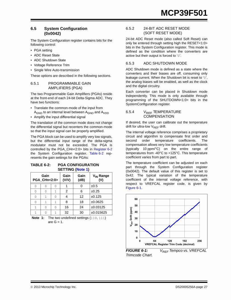
The temperature coefficient can be adjusted on eachpart through the System Configuration register(0x0042). The default value of this register is set to0x42. The typical variation of the temperaturecoefficient of the internal voltage reference, withrespect to VREFCAL register code, is given byFigure 6-1.
FIGURE 6-1: VREF Tempco vs. VREFCAL Trimcode Chart.
TABLE 6-2: PGA CONFIGURATION SETTING (Note 1)
Gain PGA_CHn<2:0>
Gain(V/V)
Gain(dB)
VIN Range (V)
0 0 0 1 0 ±0.5
0 0 1 2 6 ±0.25
0 1 0 4 12 ±0.125
0 1 1 8 18 ±0.0625
1 0 0 16 24 ±0.03125
1 0 1 32 30 ±0.015625
Note 1: The two undefined settings (110, 111) are G = 1.
0
10
20
30
40
50
60
0 64 128 192 256
V REF
Drif
t (pp
m)
VREFCAL Register Trim Code (decimal)
2013 Microchip Technology Inc. DS20005256A-page 27
MCP39F501
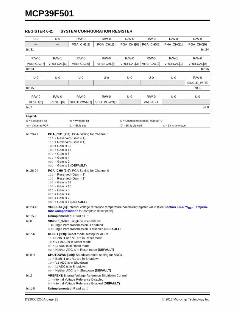
REGISTER 6-2: SYSTEM CONFIGURATION REGISTER
U-0 U-0 R/W-0 R/W-0 R/W-0 R/W-0 R/W-0 R/W-0
— — PGA_CH1[2] PGA_CH1[1] PGA_CH1[0] PGA_CH0[2] PHA_CH0[1] PGA_CH0[0]
bit 31 bit 24
R/W-0 R/W-1 R/W-0 R/W-0 R/W-0 R/W-0 R/W-1 R/W-0
VREFCAL[7] VREFCAL[6] VREFCAL[5] VREFCAL[4] VREFCAL[3] VREFCAL[2] VREFCAL[1] VREFCAL[0]
bit 23 bit 16
U-0 U-0 U-0 U-0 U-0 U-0 U-0 R/W-0
— — — — — — — SINGLE_WIRE
bit 15 bit 8
R/W-0 R/W-0 R/W-0 R/W-0 U-0 R/W-0 U-0 U-0
RESET[1] RESET[0] SHUTDOWN[1] SHUTDOWN[0] — VREFEXT — —
bit 7 bit 0
Legend:
R = Readable bit W = Writable bit U = Unimplemented bit, read as ‘0’
-n = Value at POR ‘1’ = Bit is set ‘0’ = Bit is cleared x = Bit is unknown
bit 29-27 PGA_CH1 [2:0]: PGA Setting for Channel 1111 = Reserved (Gain = 1)110 = Reserved (Gain = 1)101 = Gain is 32100 = Gain is 16011 = Gain is 8010 = Gain is 4001 = Gain is 2000 = Gain is 1 (DEFAULT)
bit 26-24 PGA_CH0 [2:0]: PGA Setting for Channel 0111 = Reserved (Gain = 1)110 = Reserved (Gain = 1)101 = Gain is 32100 = Gain is 16011 = Gain is 8010 = Gain is 4001 = Gain is 2000 = Gain is 1 (DEFAULT)
bit 23-16 VREFCAL[n]: Internal voltage reference temperature coefficient register value (See Section 6.5.4 “VREF Tempera-ture Compensation” for complete description)
bit 15-9 Unimplemented: Read as ‘0‘
bit 8 SINGLE_WIRE: single wire enable bit1 = Single Wire transmission is enabled0 = Single Wire transmission is disabled (DEFAULT)
bit 7-6 RESET [1:0]: Reset mode setting for ADCs11 = Both I1 and V1 are in Reset mode10 = V1 ADC is in Reset mode01 = I1 ADC is in Reset mode00 = Neither ADC is in Reset mode (DEFAULT)
bit 5-4 SHUTDOWN [1:0]: Shutdown mode setting for ADCs11 = Both I1 and V1 are in Shutdown10 = V1 ADC is in Shutdown01 = I1 ADC is in Shutdown00 = Neither ADC is in Shutdown (DEFAULT)
bit 2 VREFEXT: Internal Voltage Reference Shutdown Control1 = Internal Voltage Reference Disabled0 = Internal Voltage Reference Enabled (DEFAULT)
bit 1-0 Unimplemented: Read as ‘0‘
DS20005256A-page 28 2013 Microchip Technology Inc.
MCP39F501
6.6 Range Register (0x0048)
The Range register is a 32-bit register that contains thenumber of right bit shifts for the following outputs,divided into separate bytes defined below:
• RMS Current
• RMS Voltage
• Power
Note that the power range byte operates across boththe active and reactive output registers and sets thesame scale.
The purpose of this register is two-fold: the number ofright bit shifting (division by 2RANGE) must be highenough to prevent overflow in the output register, andlow enough to allow for the desired output resolution. Itis the user’s responsibility to set this register correctlyto ensure proper output operation for a given meterdesign.
For further information and example usage, seeSection 9.3 “Single Point Gain Calibrations(Calibrations at Unity Power Factor)”.
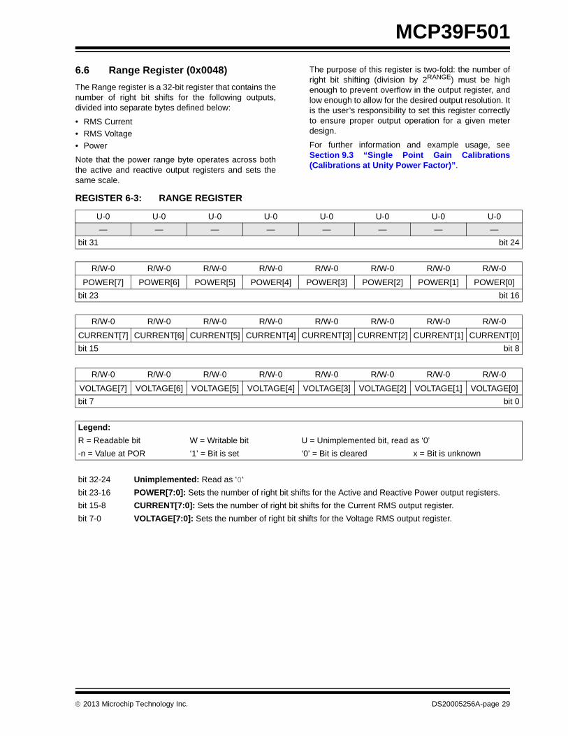
. REGISTER 6-3: RANGE REGISTER
U-0 U-0 U-0 U-0 U-0 U-0 U-0 U-0
— — — — — — — —
bit 31 bit 24
R/W-0 R/W-0 R/W-0 R/W-0 R/W-0 R/W-0 R/W-0 R/W-0
POWER[7] POWER[6] POWER[5] POWER[4] POWER[3] POWER[2] POWER[1] POWER[0]
bit 23 bit 16
R/W-0 R/W-0 R/W-0 R/W-0 R/W-0 R/W-0 R/W-0 R/W-0
CURRENT[7] CURRENT[6] CURRENT[5] CURRENT[4] CURRENT[3] CURRENT[2] CURRENT[1] CURRENT[0]
bit 15 bit 8
R/W-0 R/W-0 R/W-0 R/W-0 R/W-0 R/W-0 R/W-0 R/W-0
VOLTAGE[7] VOLTAGE[6] VOLTAGE[5] VOLTAGE[4] VOLTAGE[3] VOLTAGE[2] VOLTAGE[1] VOLTAGE[0]
bit 7 bit 0
Legend:
R = Readable bit W = Writable bit U = Unimplemented bit, read as ‘0’
-n = Value at POR ‘1’ = Bit is set ‘0’ = Bit is cleared x = Bit is unknown
bit 32-24 Unimplemented: Read as ‘0‘
bit 23-16 POWER[7:0]: Sets the number of right bit shifts for the Active and Reactive Power output registers.
bit 15-8 CURRENT[7:0]: Sets the number of right bit shifts for the Current RMS output register.
bit 7-0 VOLTAGE[7:0]: Sets the number of right bit shifts for the Voltage RMS output register.
2013 Microchip Technology Inc. DS20005256A-page 29

MCP39F501
NOTES:
DS20005256A-page 30 2013 Microchip Technology Inc.
MCP39F501
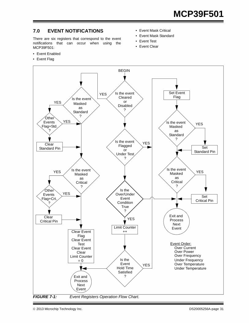
7.0 EVENT NOTIFICATIONS
There are six registers that correspond to the eventnotifications that can occur when using theMCP39F501:
• Event Enabled
• Event Flag
• Event Mask Critical
• Event Mask Standard
• Event Test
• Event Clear
FIGURE 7-1: Event Registers Operation Flow Chart.
Is the event Cleared
orDisabled
Other
Masked as
Standard
Is the event Masked
asCritical
Clear Standard Pin
Clear Critical Pin
Is the event Flagged
orUnder Test
?
?
?
?Is the
Over/UnderEvent
ConditionTrue
?
Limit Counter++
Is the Event
Hold TimeSatisfied
?
Clear EventFlag
Set EventFlag
Is the event Masked
asStandard
Is the event Masked
asCritical
?
?
SetStandard Pin
SetCritical Pin
Exit and Process
NextEvent
Exit and Process
NextEvent
YES
YES
YES
YES
YES
YES
Event Order:Over CurrentOver PowerOver FrequencyUnder FrequencyOver TemperatureUnder Temperature
YES
YES
BEGIN
Clear EventTest
Clear EventClear
Limit Counter= 0
Events Flag+Std.
?
Is the event
YES
OtherEvents
Flag+Crt.?
YES
2013 Microchip Technology Inc. DS20005256A-page 31
MCP39F501
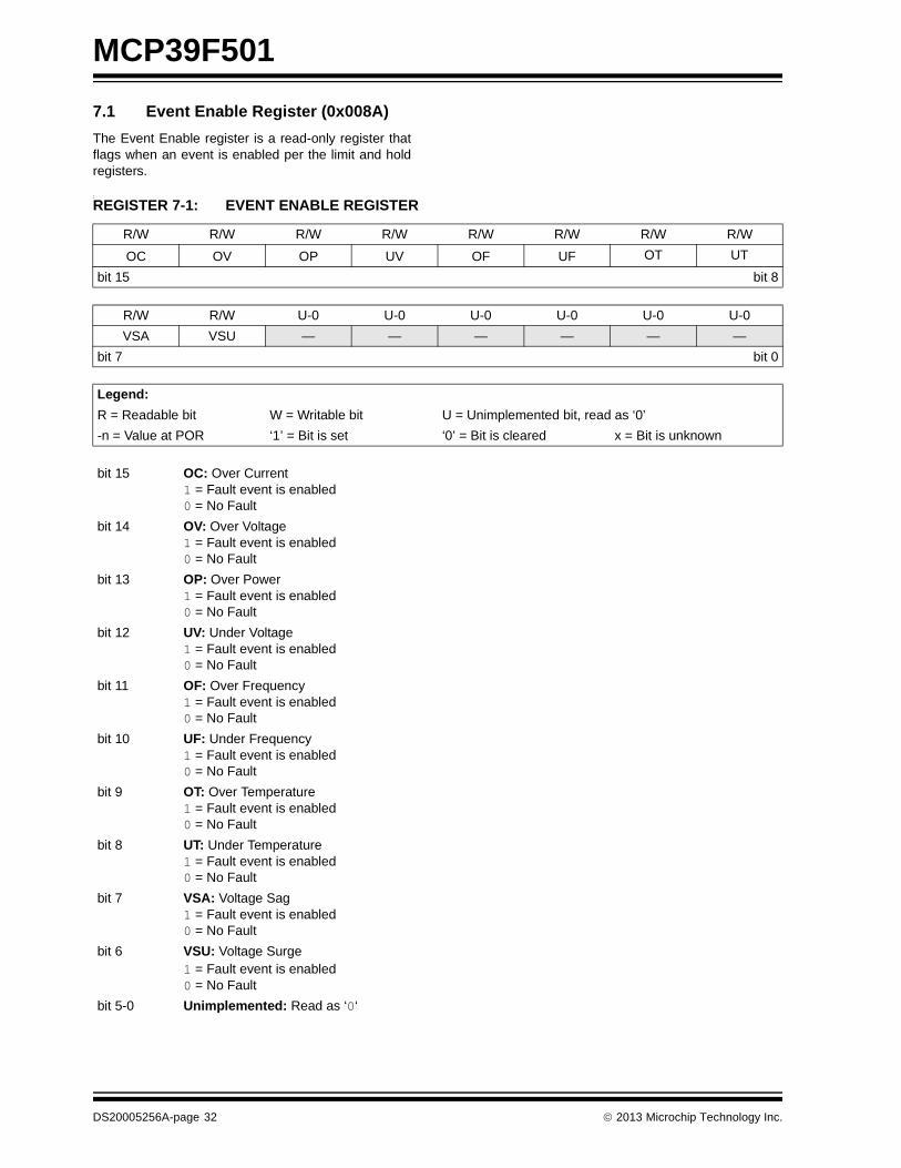
7.1 Event Enable Register (0x008A)
The Event Enable register is a read-only register thatflags when an event is enabled per the limit and holdregisters.
: REGISTER 7-1: EVENT ENABLE REGISTER
R/W R/W R/W R/W R/W R/W R/W R/W
OC OV OP UV OF UF OT UT
bit 15 bit 8
R/W R/W U-0 U-0 U-0 U-0 U-0 U-0
VSA VSU — — — — — —
bit 7 bit 0
Legend:
R = Readable bit W = Writable bit U = Unimplemented bit, read as ‘0’
-n = Value at POR ‘1’ = Bit is set ‘0’ = Bit is cleared x = Bit is unknown
bit 15 OC: Over Current1 = Fault event is enabled0 = No Fault
bit 14 OV: Over Voltage1 = Fault event is enabled0 = No Fault
bit 13 OP: Over Power1 = Fault event is enabled0 = No Fault
bit 12 UV: Under Voltage1 = Fault event is enabled0 = No Fault
bit 11 OF: Over Frequency1 = Fault event is enabled0 = No Fault
bit 10 UF: Under Frequency1 = Fault event is enabled0 = No Fault
bit 9 OT: Over Temperature1 = Fault event is enabled0 = No Fault
bit 8 UT: Under Temperature1 = Fault event is enabled0 = No Fault
bit 7 VSA: Voltage Sag1 = Fault event is enabled0 = No Fault
bit 6 VSU: Voltage Surge1 = Fault event is enabled0 = No Fault
bit 5-0 Unimplemented: Read as ‘0‘
DS20005256A-page 32 2013 Microchip Technology Inc.

MCP39F501
7.2 Event Flag Register (0x001C)
The Event Flag register is a read-only register that flagswhen an event has occurred per the limit and holdregisters.
Note that event flags are latched until the event haspassed and the bit has been cleared by the Event Clearregister.
: REGISTER 7-2: EVENT FLAG REGISTER
R-0 R-0 R-0 R-0 R-0 R-0 R-0 R-0
OC OV OP UV OF UF OT UT
bit 15 bit 8
R-0 R-0 U-0 U-0 U-0 U-0 U-0 U-0
VSA VSU — — — — — —
bit 7 bit 0
Legend:
R = Readable bit W = Writable bit U = Unimplemented bit, read as ‘0’
-n = Value at POR ‘1’ = Bit is set ‘0’ = Bit is cleared x = Bit is unknown
bit 15 OC: Over Current1 = Fault event has occurred0 = No Fault
bit 14 OV: Over Voltage1 = Fault event has occurred0 = No Fault
bit 13 OP: Over Power1 = Fault event has occurred0 = No Fault
bit 12 UV: Under Voltage1 = Fault event has occurred0 = No Fault
bit 11 OF: Over Frequency1 = Fault event has occurred0 = No Fault
bit 10 UF: Under Frequency1 = Fault event has occurred0 = No Fault
bit 9 OT: Over Temperature1 = Fault event has occurred0 = No Fault
bit 8 UT: Under Temperature1 = Fault event has occurred0 = No Fault
bit 7 VSA: Voltage Sag1 = Fault event has occurred0 = No Fault
bit 6 VSU: Voltage Surge1 = Fault event has occurred0 = No Fault
bit 5-0 Unimplemented: Read as ‘0‘
2013 Microchip Technology Inc. DS20005256A-page 33
MCP39F501
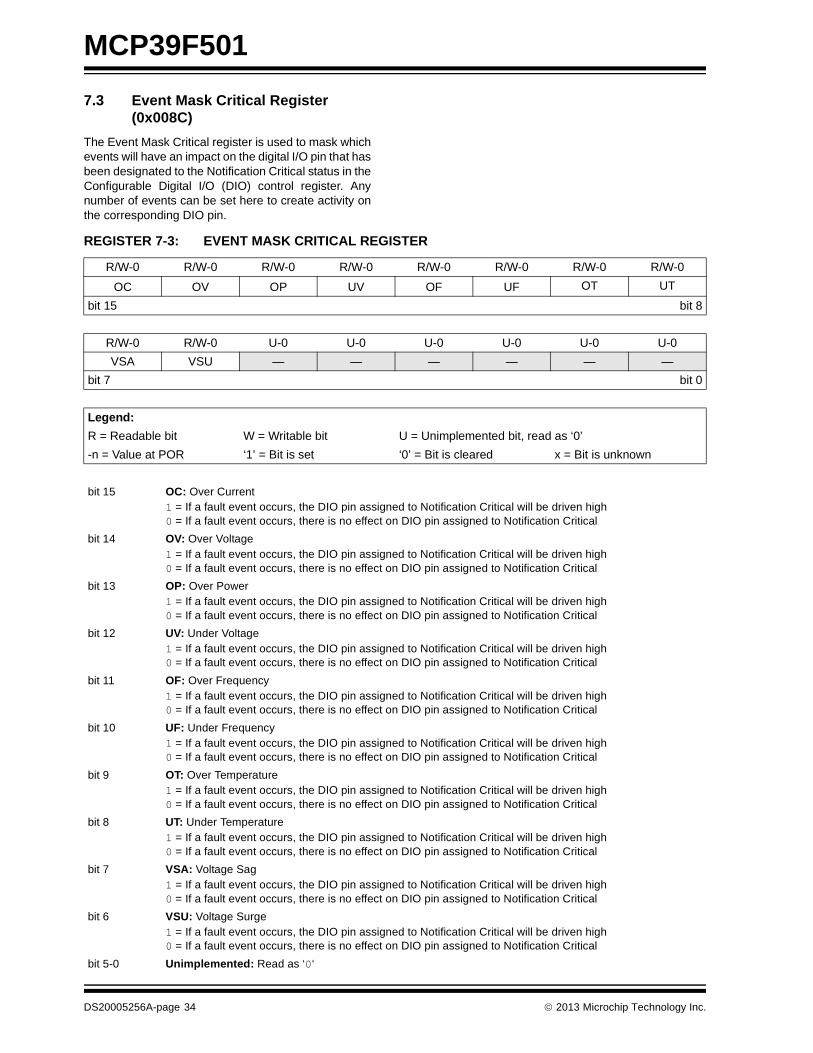
7.3 Event Mask Critical Register (0x008C)
The Event Mask Critical register is used to mask whichevents will have an impact on the digital I/O pin that hasbeen designated to the Notification Critical status in theConfigurable Digital I/O (DIO) control register. Anynumber of events can be set here to create activity onthe corresponding DIO pin. REGISTER 7-3: EVENT MASK CRITICAL REGISTER
R/W-0 R/W-0 R/W-0 R/W-0 R/W-0 R/W-0 R/W-0 R/W-0
OC OV OP UV OF UF OT UT
bit 15 bit 8
R/W-0 R/W-0 U-0 U-0 U-0 U-0 U-0 U-0
VSA VSU — — — — — —
bit 7 bit 0
Legend:
R = Readable bit W = Writable bit U = Unimplemented bit, read as ‘0’
-n = Value at POR ‘1’ = Bit is set ‘0’ = Bit is cleared x = Bit is unknown
bit 15 OC: Over Current1 = If a fault event occurs, the DIO pin assigned to Notification Critical will be driven high0 = If a fault event occurs, there is no effect on DIO pin assigned to Notification Critical
bit 14 OV: Over Voltage1 = If a fault event occurs, the DIO pin assigned to Notification Critical will be driven high0 = If a fault event occurs, there is no effect on DIO pin assigned to Notification Critical
bit 13 OP: Over Power1 = If a fault event occurs, the DIO pin assigned to Notification Critical will be driven high0 = If a fault event occurs, there is no effect on DIO pin assigned to Notification Critical
bit 12 UV: Under Voltage1 = If a fault event occurs, the DIO pin assigned to Notification Critical will be driven high0 = If a fault event occurs, there is no effect on DIO pin assigned to Notification Critical
bit 11 OF: Over Frequency1 = If a fault event occurs, the DIO pin assigned to Notification Critical will be driven high0 = If a fault event occurs, there is no effect on DIO pin assigned to Notification Critical
bit 10 UF: Under Frequency1 = If a fault event occurs, the DIO pin assigned to Notification Critical will be driven high0 = If a fault event occurs, there is no effect on DIO pin assigned to Notification Critical
bit 9 OT: Over Temperature1 = If a fault event occurs, the DIO pin assigned to Notification Critical will be driven high0 = If a fault event occurs, there is no effect on DIO pin assigned to Notification Critical
bit 8 UT: Under Temperature1 = If a fault event occurs, the DIO pin assigned to Notification Critical will be driven high0 = If a fault event occurs, there is no effect on DIO pin assigned to Notification Critical
bit 7 VSA: Voltage Sag1 = If a fault event occurs, the DIO pin assigned to Notification Critical will be driven high0 = If a fault event occurs, there is no effect on DIO pin assigned to Notification Critical
bit 6 VSU: Voltage Surge1 = If a fault event occurs, the DIO pin assigned to Notification Critical will be driven high0 = If a fault event occurs, there is no effect on DIO pin assigned to Notification Critical
bit 5-0 Unimplemented: Read as ‘0‘
DS20005256A-page 34 2013 Microchip Technology Inc.
MCP39F501
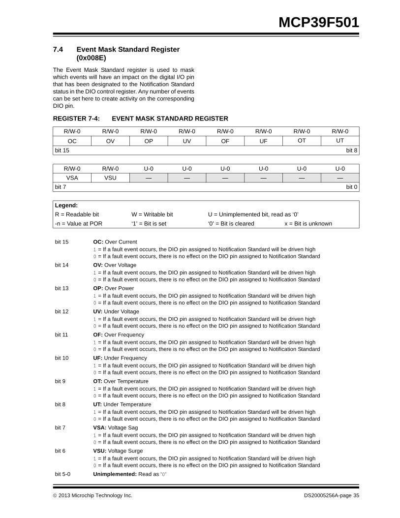
7.4 Event Mask Standard Register (0x008E)
The Event Mask Standard register is used to maskwhich events will have an impact on the digital I/O pinthat has been designated to the Notification Standardstatus in the DIO control register. Any number of eventscan be set here to create activity on the correspondingDIO pin. REGISTER 7-4: EVENT MASK STANDARD REGISTER
R/W-0 R/W-0 R/W-0 R/W-0 R/W-0 R/W-0 R/W-0 R/W-0
OC OV OP UV OF UF OT UT
bit 15 bit 8
R/W-0 R/W-0 U-0 U-0 U-0 U-0 U-0 U-0
VSA VSU — — — — — —
bit 7 bit 0
Legend:
R = Readable bit W = Writable bit U = Unimplemented bit, read as ‘0’
-n = Value at POR ‘1’ = Bit is set ‘0’ = Bit is cleared x = Bit is unknown
bit 15 OC: Over Current1 = If a fault event occurs, the DIO pin assigned to Notification Standard will be driven high0 = If a fault event occurs, there is no effect on the DIO pin assigned to Notification Standard
bit 14 OV: Over Voltage1 = If a fault event occurs, the DIO pin assigned to Notification Standard will be driven high0 = If a fault event occurs, there is no effect on the DIO pin assigned to Notification Standard
bit 13 OP: Over Power1 = If a fault event occurs, the DIO pin assigned to Notification Standard will be driven high0 = If a fault event occurs, there is no effect on the DIO pin assigned to Notification Standard
bit 12 UV: Under Voltage1 = If a fault event occurs, the DIO pin assigned to Notification Standard will be driven high0 = If a fault event occurs, there is no effect on the DIO pin assigned to Notification Standard
bit 11 OF: Over Frequency1 = If a fault event occurs, the DIO pin assigned to Notification Standard will be driven high0 = If a fault event occurs, there is no effect on the DIO pin assigned to Notification Standard
bit 10 UF: Under Frequency1 = If a fault event occurs, the DIO pin assigned to Notification Standard will be driven high0 = If a fault event occurs, there is no effect on the DIO pin assigned to Notification Standard
bit 9 OT: Over Temperature1 = If a fault event occurs, the DIO pin assigned to Notification Standard will be driven high0 = If a fault event occurs, there is no effect on the DIO pin assigned to Notification Standard
bit 8 UT: Under Temperature1 = If a fault event occurs, the DIO pin assigned to Notification Standard will be driven high0 = If a fault event occurs, there is no effect on the DIO pin assigned to Notification Standard
bit 7 VSA: Voltage Sag1 = If a fault event occurs, the DIO pin assigned to Notification Standard will be driven high0 = If a fault event occurs, there is no effect on the DIO pin assigned to Notification Standard
bit 6 VSU: Voltage Surge1 = If a fault event occurs, the DIO pin assigned to Notification Standard will be driven high0 = If a fault event occurs, there is no effect on the DIO pin assigned to Notification Standard
bit 5-0 Unimplemented: Read as ‘0‘
2013 Microchip Technology Inc. DS20005256A-page 35
MCP39F501
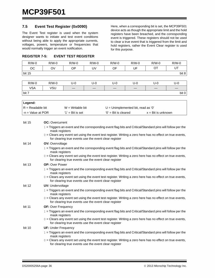
7.5 Event Test Register (0x0090)
The Event Test register is used when the systemdesigner wants to initiate and test event conditionswithout being able to apply the appropriate currents,voltages, powers, temperature or frequencies thatwould normally trigger an event notification.
Here, when a corresponding bit is set, the MCP39F501device acts as though the appropriate limit and the holdregisters have been breached, and the correspondingevent is triggered. These registers should not be usedto clear a true event that is triggered from the limit andhold registers, rather the Event Clear register is usedfor this purpose.
: REGISTER 7-5: EVENT TEST REGISTER
R/W-0 R/W-0 R/W-0 R/W-0 R/W-0 R/W-0 R/W-0 R/W-0
OC OV OP UV OF UF OT UT
bit 15 bit 8
R/W-0 R/W-0 U-0 U-0 U-0 U-0 U-0 U-0
VSA VSU — — — — — —
bit 7 bit 0
Legend:
R = Readable bit W = Writable bit U = Unimplemented bit, read as ‘0’
-n = Value at POR ‘1’ = Bit is set ‘0’ = Bit is cleared x = Bit is unknown
bit 15 OC: Overcurrent
1 = Triggers an event and the corresponding event flag bits and Critical/Standard pins will follow per themask registers
0 = Clears any event set using the event test register. Writing a zero here has no effect on true events,for clearing true events use the event clear register
bit 14 OV: Overvoltage
1 = Triggers an event and the corresponding event flag bits and Critical/Standard pins will follow per themask registers
0 = Clears any event set using the event test register. Writing a zero here has no effect on true events,for clearing true events use the event clear register
bit 13 OP: Over Power
1 = Triggers an event and the corresponding event flag bits and Critical/Standard pins will follow per themask registers
0 = Clears any event set using the event test register. Writing a zero here has no effect on true events,for clearing true events use the event clear register
bit 12 UV: Undervoltage
1 = Triggers an event and the corresponding event flag bits and Critical/Standard pins will follow per themask registers
0 = Clears any event set using the event test register. Writing a zero here has no effect on true events,for clearing true events use the event clear register
bit 11 OF: Over Frequency
1 = Triggers an event and the corresponding event flag bits and Critical/Standard pins will follow per themask registers
0 = Clears any event set using the event test register. Writing a zero here has no effect on true events,for clearing true events use the event clear register
bit 10 UF: Under Frequency
1 = Triggers an event and the corresponding event flag bits and Critical/Standard pins will follow per themask registers
0 = Clears any event set using the event test register. Writing a zero here has no effect on true events,for clearing true events use the event clear register
DS20005256A-page 36 2013 Microchip Technology Inc.
MCP39F501
7.6 Event Clear Register (0x0092)
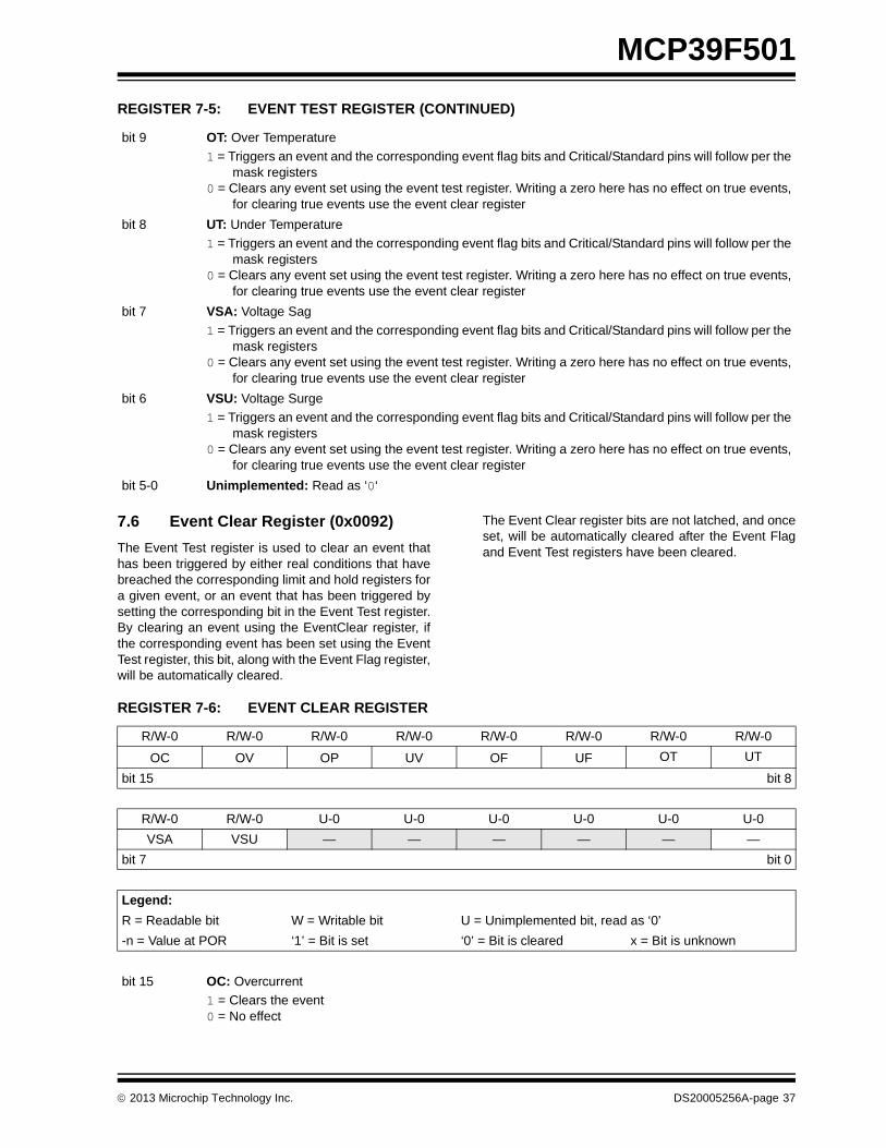
The Event Test register is used to clear an event thathas been triggered by either real conditions that havebreached the corresponding limit and hold registers fora given event, or an event that has been triggered bysetting the corresponding bit in the Event Test register.By clearing an event using the EventClear register, ifthe corresponding event has been set using the EventTest register, this bit, along with the Event Flag register,will be automatically cleared.
The Event Clear register bits are not latched, and onceset, will be automatically cleared after the Event Flagand Event Test registers have been cleared.
bit 9 OT: Over Temperature
1 = Triggers an event and the corresponding event flag bits and Critical/Standard pins will follow per themask registers
0 = Clears any event set using the event test register. Writing a zero here has no effect on true events,for clearing true events use the event clear register
bit 8 UT: Under Temperature
1 = Triggers an event and the corresponding event flag bits and Critical/Standard pins will follow per themask registers
0 = Clears any event set using the event test register. Writing a zero here has no effect on true events,for clearing true events use the event clear register
bit 7 VSA: Voltage Sag
1 = Triggers an event and the corresponding event flag bits and Critical/Standard pins will follow per themask registers
0 = Clears any event set using the event test register. Writing a zero here has no effect on true events,for clearing true events use the event clear register
bit 6 VSU: Voltage Surge
1 = Triggers an event and the corresponding event flag bits and Critical/Standard pins will follow per themask registers
0 = Clears any event set using the event test register. Writing a zero here has no effect on true events,for clearing true events use the event clear register
bit 5-0 Unimplemented: Read as ‘0‘
REGISTER 7-5: EVENT TEST REGISTER (CONTINUED)
REGISTER 7-6: EVENT CLEAR REGISTER
R/W-0 R/W-0 R/W-0 R/W-0 R/W-0 R/W-0 R/W-0 R/W-0
OC OV OP UV OF UF OT UT
bit 15 bit 8
R/W-0 R/W-0 U-0 U-0 U-0 U-0 U-0 U-0
VSA VSU — — — — — —
bit 7 bit 0
Legend:
R = Readable bit W = Writable bit U = Unimplemented bit, read as ‘0’
-n = Value at POR ‘1’ = Bit is set ‘0’ = Bit is cleared x = Bit is unknown
bit 15 OC: Overcurrent
1 = Clears the event0 = No effect
2013 Microchip Technology Inc. DS20005256A-page 37
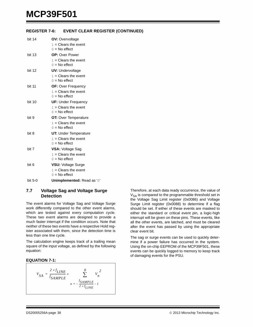
MCP39F501
7.7 Voltage Sag and Voltage Surge Detection
The event alarms for Voltage Sag and Voltage Surgework differently compared to the other event alarms,which are tested against every computation cycle.These two event alarms are designed to provide amuch faster interrupt if the condition occurs. Note thatneither of these two events have a respective Hold reg-ister associated with them, since the detection time isless than one line cycle.
The calculation engine keeps track of a trailing meansquare of the input voltage, as defined by the followingequation:
EQUATION 7-1:
Therefore, at each data ready occurrence, the value ofVSA is compared to the programmable threshold set inthe Voltage Sag Limit register (0x0086) and VoltageSurge Limit register (0x0088) to determine if a flagshould be set. If either of these events are masked toeither the standard or critical event pin, a logic-highinterrupt will be given on these pins. These events, likeall the other events, are latched, and must be clearedafter the event has passed by using the appropriateclear event bit.
The sag or surge events can be used to quickly deter-mine if a power failure has occurred in the system.Using the on-chip EEPROM of the MCP39F501, theseevents can be quickly logged to memory to keep trackof damaging events for the PSU.
bit 14 OV: Overvoltage
1 = Clears the event0 = No effect
bit 13 OP: Over Power
1 = Clears the event0 = No effect
bit 12 UV: Undervoltage
1 = Clears the event0 = No effect
bit 11 OF: Over Frequency
1 = Clears the event0 = No effect
bit 10 UF: Under Frequency
1 = Clears the event0 = No effect
bit 9 OT: Over Temperature
1 = Clears the event0 = No effect
bit 8 UT: Under Temperature
1 = Clears the event0 = No effect
bit 7 VSA: Voltage Sag
1 = Clears the event0 = No effect
bit 6 VSU: Voltage Surge
1 = Clears the event0 = No effect
bit 5-0 Unimplemented: Read as ‘0‘
REGISTER 7-6: EVENT CLEAR REGISTER (CONTINUED)
VSA
2 f LINEfSAMPLE-------------------------- Vn
nfSAMPLE2 fLINE--------------------------– 1–=
0
2
=
DS20005256A-page 38 2013 Microchip Technology Inc.
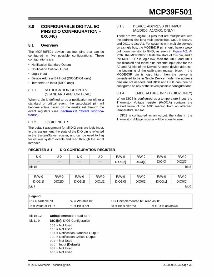
MCP39F501
8.0 CONFIGURABLE DIGITAL I/O PINS (DIO CONFIGURATION – 0X0046)
8.1 Overview
The MCP39F501 device has four pins that can beconfigured in five possible configurations. Theseconfigurations are:
• Notification Standard Output
• Notification Critical Output
• Logic Input
• Device Address Bit Input (DIO0/DIO1 only)
• Temperature Input (DIO2 only)
8.1.1 NOTIFICATION OUTPUTS (STANDARD AND CRITICAL)
When a pin is defined to be a notification for either astandard or critical event, the associated pin willbecome active based on the masks set through theevent registers (see Section 7.0 “Event Notifica-tions”).
8.1.2 LOGIC INPUTS
The default assignment for all DIO pins are logic input.In this assignment, the state of the DIO pin is reflectedin the SystemStatus register, and can be used to flagfor various system events and read through the serialinterface.
8.1.3 DEVICE ADDRESS BIT INPUT(A0/DIO0, A1/DIO1 ONLY)
There are two digital IO pins that are multiplexed withthe address pins for a multi-device bus. DIO0 is also A0and DIO1 is also A1. For systems with multiple deviceson a single bus, the MODE/DIR pin should have a weakpull-down resistor to GND, as seen in Figure 4-2. AtPOR, the MCP39F501 tests the state of this pin, and ifthe MODE/DIR is logic low, then the DIO0 and DIO1are disabled and these pins become input pins for theA0 and A1 bits of the Device Address device address,the beginning of the calibration register block. If theMODE/DIR pin is logic high, then the device isconsidered to be in Single Device mode, the addresspins are not needed, and DIO0 and DIO1 can then beconfigured as any of the seven possible configurations.
8.1.4 TEMPERATURE INPUT (DIO2 ONLY)
When DIO2 is configured as a temperature input, theThermistor Voltage register (0x001A) contains thescaled value of the ADC reading from an attachedtemperature sensor.
If DIO2 is configured as an output, the value in theThermistor Voltage register will be equal to zero.
REGISTER 8-1: DIO CONFIGURATION REGISTER
U-0 U-0 U-0 U-0 R/W-0 R/W-0 R/W-0 R/W-0
— — — — DIO3[2] DIO3[1] DIO[0] DIO2[2]
bit 15 bit 8
R/W-0 R/W-0 R/W-0 R/W-0 R/W-0 R/W-0 R/W-0 R/W-0
DIO2[1] DIO2[0] DIO1[2] DIO1[1] DIO1[0] DIO0[2] DIO0[1] DIO0[0]
bit 7 bit 0
Legend:
R = Readable bit W = Writable bit U = Unimplemented bit, read as ‘0’
-n = Value at POR ‘1’ = Bit is set ‘0’ = Bit is cleared x = Bit is unknown
bit 15-12 Unimplemented: Read as ‘0‘
bit 11-9 DIO3[n]: DIO3 Configuration
111 = Not Used110 = Not Used101 = Notification Standard Output100 = Notification Critical Output011 = Not Used010 = Input (Default)001 = Not Used000 = Not Used
2013 Microchip Technology Inc. DS20005256A-page 39
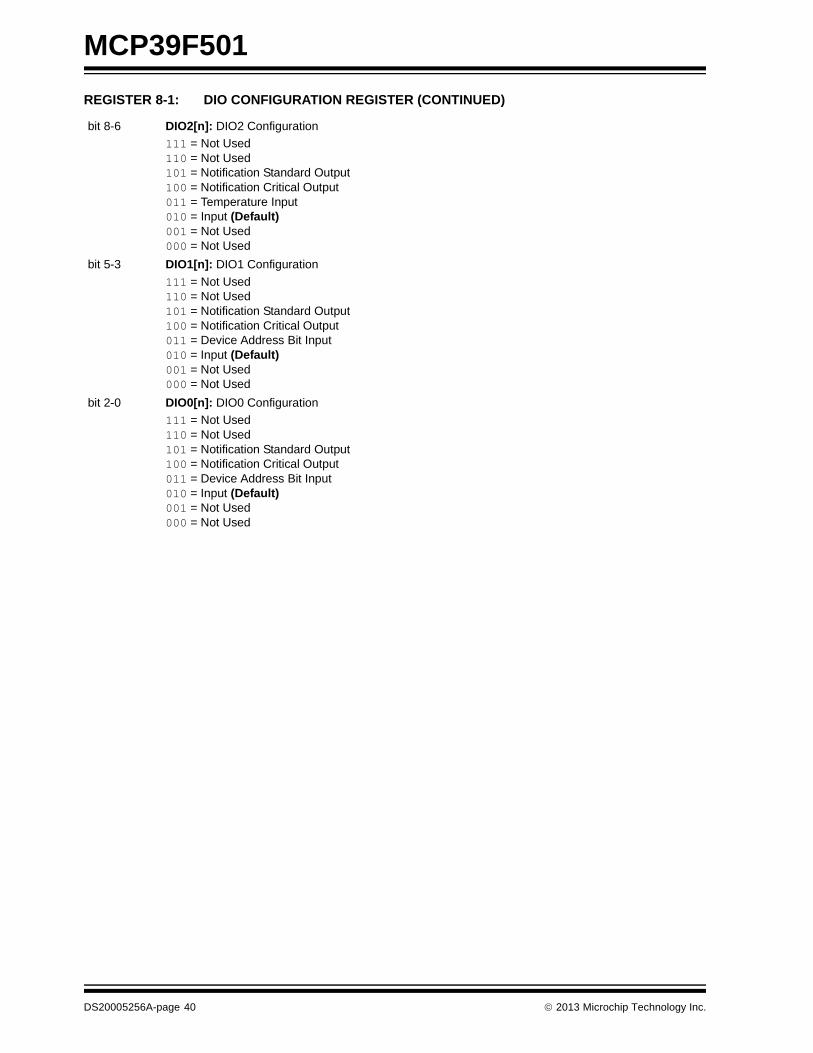
MCP39F501
bit 8-6 DIO2[n]: DIO2 Configuration
111 = Not Used110 = Not Used101 = Notification Standard Output100 = Notification Critical Output011 = Temperature Input010 = Input (Default)001 = Not Used000 = Not Used
bit 5-3 DIO1[n]: DIO1 Configuration
111 = Not Used110 = Not Used101 = Notification Standard Output100 = Notification Critical Output011 = Device Address Bit Input 010 = Input (Default)001 = Not Used000 = Not Used
bit 2-0 DIO0[n]: DIO0 Configuration
111 = Not Used110 = Not Used101 = Notification Standard Output100 = Notification Critical Output011 = Device Address Bit Input010 = Input (Default)001 = Not Used000 = Not Used
REGISTER 8-1: DIO CONFIGURATION REGISTER (CONTINUED)
DS20005256A-page 40 2013 Microchip Technology Inc.
MCP39F501
9.0 MCP39F501 CALIBRATION
9.1 Overview
Calibration compensates for ADC gain error, compo-nent tolerances and overall noise in the system. Thedevice provides an on-chip calibration algorithm thatallows simple system calibration to be performedquickly. The excellent analog performance of the A/Dconverters on the MCP39F501 allows for a single pointcalibration and a single calibration command toachieve accurate measurements.
Calibration can be done by either using the predefinedauto-calibration commands, or by writing directly to thecalibration registers. If additional calibration points arerequired (AC offset, Phase Compensation, DC offset),the corresponding calibration registers are available tothe user and will be described separately in thissection.
9.2 Calibration Order
The proper steps for calibration need to be maintained.
If the device has an external temperature sensorattached, temperature calibration should be done firstby reading the value from the Thermistor Voltageregister (0x001A) and copying the value by writing tothe Ambient Temperature Reference Voltage register(0x00B6).
If the device runs on the internal oscillator, the linefrequency must be calibrated next using the Auto-Calibration Frequency command.
The single point gain calibration at unity power factorshould be performed next.
If non-unity displacement power factor measurementsare a concern, then the next step should be phasecalibration, followed by reactive power gain calibration.
To summarize the order of calibration:
1. Temperature Calibration (optional)
2. Line Frequency Calibration (optional)
3. Gain Calibration at PF = 1
4. Phase Calibration at PF 1 (optional)
5. Reactive Gain Calibration at PF 1(optional)
9.3 Single Point Gain Calibrations (Calibrations at Unity Power Factor)
When using the device in AC mode with the high-passfilters turned on, most offset errors are removed andonly a single point gain calibration is required.
Setting the gain registers to properly produce thedesired outputs can be done manually by writing to theappropriate register. The alternative method is to usethe auto-calibration commands described in thissection.
9.3.1 USING THE Auto-Calibration Gain COMMAND
By applying stable reference voltages and currents thatare equivalent to the values that reside in the targetCalibration Current (0x004C), Calibration Voltage(0x0050) and Calibration Active Power (0x0052)registers, the Auto-Calibration Gain commandcan then be issued to the device.
After a successful calibration (response = ACK), aSave Registers to Flash command can then beissued to save the calibration constants calculated bythe device.
The following registers are set when the Auto-Cali-bration Gain command is issued:
• Gain Current RMS (0x0028)
• Gain Voltage RMS (0x002A)
• Gain Active Power (0x002C)
When this command is issued, the MCP39F501attempts to match the expected values to the mea-sured values for all three output quantities by changingthe gain register based on the following formula:
EQUATION 9-1:
The same formula applies for voltage RMS, currentRMS and active power. Since the gain registers for allthree quantities are 16-bit numbers, the ratio of theexpected value to the measured value (which can bemodified by changing the Range register) and theprevious gain must be such that the equation yields avalid number. Here the limits are set to be from 25,000to 65,535. A new gain within this range for all threelimits will return an ACK for a successful calibration,otherwise the command returns a NAK for a failedcalibration attempt.
It is the user’s responsibility to ensure that the properrange settings, PGA settings and hardware designsettings are correct to allow for successful calibrationusing this command.
9.3.2 EXAMPLE OF RANGE SELECTION FOR VALID CALIBRATION
In this example, a user applies a calibration current of1A to an uncalibrated system. The indicated value inthe Current RMS register (0x0004) is 2300 with thesystem's specific shunt value, PGA gain, etc. The userexpects to see a value of 1000 in the Current RMSregister when 1A current is applied, meaning 1.000 Awith 1 mA resolution. Other given values are:
• The existing value for Gain Current RMS is 33480.
• The existing value for Range is 12.
GAINNEW GAINOLDExpectedMeasured--------------------------=
2013 Microchip Technology Inc. DS20005256A-page 41
MCP39F501
By using Equation 9-1, the calculation for GainNEWyields:
EQUATION 9-2:
When using the Auto-Calibration Gain com-mand, the result would be a failed calibration or a NAKreturned form the MCP39F501, because the resultingGainNEW is less than 20,000.
The solution is to use the Range register to bring themeasured value closer to the expected value, suchthat a new gain value can be calculated within thelimits specified above.
The Range register specifies the number of right-bitshifts (equivalent to divisions by 2) after themultiplication with the Gain Current RMS register.Refer to Section 5.0 “Calculation Engine (CE)Description” for information on the Range register.
Incrementing the Range register by 1 unit, an addi-tional right-bit shift or ÷2 is included in the calculation.Increasing the current range from 12 to 13 yields thenew measured Current RMS register value of 2300/2= 1150. The expected (1000) and measured (1150)are much closer now, so the expected new gainshould be within the limits:
EQUATION 9-3:
The resulting new gain is within the limits and thedevice successfully calibrates Current RMS andreturns an ACK.
It can be observed that the range can be set to 14 andthe resulting new gain will still be within limits(GainNEW = 58226). However, since this gain value isclose to the limit of the 16-bit Gain register, variationsfrom system to system (component tolerances, etc.)might create a scenario where the calibration is notsuccessful on some units and there would be a yieldissue. The best approach is to choose a range valuethat places the new gain in the middle of the bounds ofthe gain registers described above.
In a second example, when applying 1A, the userexpects an output of 1.0000A with 0.1 mA resolution.The example is starting with the same initial values:
EQUATION 9-4:
The GainNEW is much larger than the 16-bit limit of65535, so fewer right-bit shifts must be introduced toget the measured value closer to the expected value.The user needs to compute the number of bit shiftsthat will give a value lower than 65535. To estimatethis number:
EQUATION 9-5:
2.2 rounds to the closest integer value of 2. The rangevalue changes to 12 – 2 = 10; there are 2 less right-bitshifts.
The new measured value will be 2300 x 22 = 9200.
EQUATION 9-6:
The resulting new gain is within the limits and thedevice successfully calibrates Current RMS andreturns an ACK.
9.4 Calibrating the Phase Compensation Register (0x003E)
Phase compensation is provided to adjust for anyphase delay between the current and voltage path.This procedure requires sinusoidal current and voltagewaveforms, with a significant phase shift betweenthem, and significant amplitudes. The recommendeddisplacement power factor for calibration is 0.5. Theprocedure for calculating the phase compensationregister is the following:
1. Determine what is the difference between theangle corresponding to the measured powerfactor (PFMEAS) and the angle corresponding tothe expected power factor (PFEXP), in degrees.
EQUATION 9-7:
2. Convert this from degrees to the resolutionprovided by the Equation 9-8:
EQUATION 9-8:
GAINNEW GAINOLDExpectedMeasured--------------------------- 33480
10002300------------ 14556===
14556 20000
GAINNEW GAINOLDExpectedMeasured--------------------------- 33480
10001150------------ 29113===
20000 29113 65535
GAINNEW GAINOLDExpectedMeasured--------------------------- 33480
10002300------------ 145565===
145565 65535
14556565535
------------------ 2.2=
GAINNEW GAINOLDExpectedMeasured--------------------------- 33480
100009200
--------------- 36391===
20000 36391 65535
PFMEASValue in PowerFactor Register
32768---------------------------------------------------------------------------=
ANGLEMEAS PFMEAS 180
---------acos=
ANGLEEXP PFEXP 180
---------acos=
ANGLEMEAS ANGLEEXP– 40=
DS20005256A-page 42 2013 Microchip Technology Inc.
MCP39F501
3. Combine this additional phase compensation towhatever value is currently in the phasecompensation, and update the register.Equation 9-9 should be computed in terms of a8-bit 2's complement signed value. The 8-bitresult is placed in the least significant byte of the16-bit Phase Compensation register (0x003E).
EQUATION 9-9:
Based on Equation 9-9, the maximum angle in degreesthat can be compensated is ±3.2 degrees. If a largerphase shift is required, contact your local Microchipsales office.
9.5 Reactive Power Calibration and Phase Compensation (Calibrations at Non-unity Power Factor)
In order to correctly calibrate the reactive powercalculation through the Gain Reactive Power register(0x002E), and to properly correct for any phase errorthrough the Phase Compensation register, thecalibration must be done at a power factor other thanPF = 1, typically at PF = 0.5.
9.5.1 USING THE AUTO-CALIBRATION REACTIVE GAIN COMMAND
By applying the equivalent current, voltage and phaselag (or lead) that correspond to the target reactivepower in the Calibration Reactive Power register(0x0056), the Auto-Calibration Gain command(0x7A) can be issued to the device.
After a successful calibration (response = ACK), aSave Registers to Flash command can then beissued to save the calibration constants calculated bythe device.
The following register is set when theAuto-Calibration Gain command is issued:
• Gain Reactive Power
When this command is issued, the MCP39F501attempts to match the expected value of the reactivepower to the measured value of reactive power bychanging the GainReactivePower register.
9.6 Offset/No Load Calibrations
During offset calibrations, no line voltage or currentshould be applied to the system. The system should bein a No Load condition.
9.6.1 AC OFFSET CALIBRATION
There are three registers associated with the AC OffsetCalibration:
• Offset Current RMS(0x0030)
• Offset Active Power(0x0034)
• Offset Reactive Power(0x0038)
When computing the AC offset values, the respectivegain and Range registers should be taken intoconsideration according to the block diagrams inFigures 5-2, 5-3 and 5-4.
After a successful offset calibration, a SaveRegisters to Flash command can then be issuedto save the calibration constants calculated by thedevice.
9.6.2 DC OFFSET CALIBRATION
In DC applications, the high-pass filter on the currentand voltage channels is turned off. To remove anyresidual DC value on the current, the DCOffsetCurrent(0x003C) register adds to the A/D conversionimmediately after the ADC and prior to any otherfunction.
9.7 Calibrating the Line Frequency Register (0x0018)
The Line Frequency register contains a 16-bit numberwith a value equivalent to the input line frequency as itis measured on the voltage channel. When in DCmode, this calculation is turned off and the register willbe equal to zero.
The measurement of the line frequency is only validfrom 45 to 65 Hz.
9.7.1 USING THE Auto-Calibration Frequency COMMAND
By a applying stable reference voltage with a constantline frequency that is equivalent to the value that residein the Line Frequency Ref (0x0094), the Auto-Cali-bration Frequency command can then be issuedto the device.
After a successful calibration (response = ACK), aSave Registers to Flash command can then beissued to save the calibration constants calculated bythe device.
The following register is set when the Auto-Cali-bration Frequency command is issued:
• Gain Line Frequency (0x00AE)
Note that the command is only required when runningoff the internal oscillator. The formula used to calculatethe new gain is given in Equation 9-1.
PhaseCompensationNEW PhaseCompensationOLD +=
2013 Microchip Technology Inc. DS20005256A-page 43
MCP39F501
9.8 Temperature Compensation (Addresses 0x00B0/B2/B4/B6)
MCP39F501 measures the indication of the tempera-ture sensor and uses the value to compensate the tem-perature variation of the shunt resistance and thefrequency of the internal RC oscillator.
The same formula applies for Line Frequency, CurrentRMS, Active Power and Reactive Power. Thetemperature compensation coefficient depends on the16-bit signed integer value of the correspondingcompensation register.
EQUATION 9-10:
At the calibration temperature, the effect of the com-pensation coefficients is minimal. The coefficients needto be tuned when the difference between the calibrationtemperature and the device temperature is significant.It is recommended to use the default values as startingpoints.
y x 1 c T TCAL– + =
Where:
x = Uncompensated Output (corresponding to Line Frequency, Current RMS, Active Power and Reactive Power)
y = Compensated Output
c = Temperature Compensation Coefficient (depending on the shunt's Temperature Coefficient of Resistance or on the internal RC oscillator temperature frequency drift)
T = Thermistor Voltage (in 10-bit ADC units)
TCAL = Ambient Temperature Reference Voltage. It should be set at the beginning of the calibration procedure, by reading the thermistor voltage and writing its value to the ambient temperature reference voltage register.
M = 26 (for Line Frequency compensation)
= 27 (for Current, Active Power and Reactive Power)
cTemperatureCompensation Register
2M
-----------------------------------------------------------------------------------------------=
DS20005256A-page 44 2013 Microchip Technology Inc.
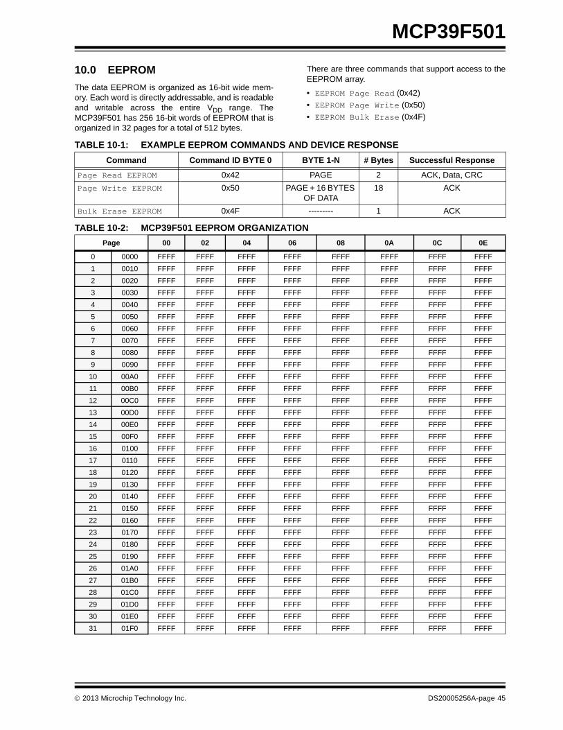
MCP39F501
10.0 EEPROM
The data EEPROM is organized as 16-bit wide mem-ory. Each word is directly addressable, and is readableand writable across the entire VDD range. TheMCP39F501 has 256 16-bit words of EEPROM that isorganized in 32 pages for a total of 512 bytes.
There are three commands that support access to theEEPROM array.
• EEPROM Page Read (0x42)
• EEPROM Page Write (0x50)
• EEPROM Bulk Erase (0x4F)
TABLE 10-1: EXAMPLE EEPROM COMMANDS AND DEVICE RESPONSE
Command Command ID BYTE 0 BYTE 1-N # Bytes Successful Response
Page Read EEPROM 0x42 PAGE 2 ACK, Data, CRC
Page Write EEPROM 0x50 PAGE + 16 BYTES OF DATA
18 ACK
Bulk Erase EEPROM 0x4F --------- 1 ACK
TABLE 10-2: MCP39F501 EEPROM ORGANIZATION
Page 00 02 04 06 08 0A 0C 0E
0 0000 FFFF FFFF FFFF FFFF FFFF FFFF FFFF FFFF
1 0010 FFFF FFFF FFFF FFFF FFFF FFFF FFFF FFFF
2 0020 FFFF FFFF FFFF FFFF FFFF FFFF FFFF FFFF
3 0030 FFFF FFFF FFFF FFFF FFFF FFFF FFFF FFFF
4 0040 FFFF FFFF FFFF FFFF FFFF FFFF FFFF FFFF
5 0050 FFFF FFFF FFFF FFFF FFFF FFFF FFFF FFFF
6 0060 FFFF FFFF FFFF FFFF FFFF FFFF FFFF FFFF
7 0070 FFFF FFFF FFFF FFFF FFFF FFFF FFFF FFFF
8 0080 FFFF FFFF FFFF FFFF FFFF FFFF FFFF FFFF
9 0090 FFFF FFFF FFFF FFFF FFFF FFFF FFFF FFFF
10 00A0 FFFF FFFF FFFF FFFF FFFF FFFF FFFF FFFF
11 00B0 FFFF FFFF FFFF FFFF FFFF FFFF FFFF FFFF
12 00C0 FFFF FFFF FFFF FFFF FFFF FFFF FFFF FFFF
13 00D0 FFFF FFFF FFFF FFFF FFFF FFFF FFFF FFFF
14 00E0 FFFF FFFF FFFF FFFF FFFF FFFF FFFF FFFF
15 00F0 FFFF FFFF FFFF FFFF FFFF FFFF FFFF FFFF
16 0100 FFFF FFFF FFFF FFFF FFFF FFFF FFFF FFFF
17 0110 FFFF FFFF FFFF FFFF FFFF FFFF FFFF FFFF
18 0120 FFFF FFFF FFFF FFFF FFFF FFFF FFFF FFFF
19 0130 FFFF FFFF FFFF FFFF FFFF FFFF FFFF FFFF
20 0140 FFFF FFFF FFFF FFFF FFFF FFFF FFFF FFFF
21 0150 FFFF FFFF FFFF FFFF FFFF FFFF FFFF FFFF
22 0160 FFFF FFFF FFFF FFFF FFFF FFFF FFFF FFFF
23 0170 FFFF FFFF FFFF FFFF FFFF FFFF FFFF FFFF
24 0180 FFFF FFFF FFFF FFFF FFFF FFFF FFFF FFFF
25 0190 FFFF FFFF FFFF FFFF FFFF FFFF FFFF FFFF
26 01A0 FFFF FFFF FFFF FFFF FFFF FFFF FFFF FFFF
27 01B0 FFFF FFFF FFFF FFFF FFFF FFFF FFFF FFFF
28 01C0 FFFF FFFF FFFF FFFF FFFF FFFF FFFF FFFF
29 01D0 FFFF FFFF FFFF FFFF FFFF FFFF FFFF FFFF
30 01E0 FFFF FFFF FFFF FFFF FFFF FFFF FFFF FFFF
31 01F0 FFFF FFFF FFFF FFFF FFFF FFFF FFFF FFFF
2013 Microchip Technology Inc. DS20005256A-page 45

MCP39F501
NOTES:
DS20005256A-page 46 2013 Microchip Technology Inc.
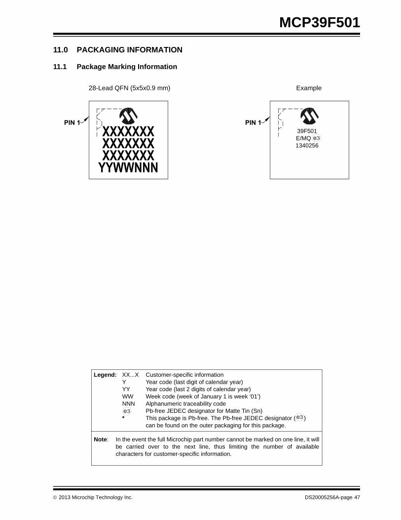
MCP39F501
11.0 PACKAGING INFORMATION
11.1 Package Marking Information
28-Lead QFN (5x5x0.9 mm) Example
PIN 1 PIN 1
Legend: XX...X Customer-specific informationY Year code (last digit of calendar year)YY Year code (last 2 digits of calendar year)WW Week code (week of January 1 is week ‘01’)NNN Alphanumeric traceability code Pb-free JEDEC designator for Matte Tin (Sn)* This package is Pb-free. The Pb-free JEDEC designator ( )
can be found on the outer packaging for this package.
Note: In the event the full Microchip part number cannot be marked on one line, it willbe carried over to the next line, thus limiting the number of availablecharacters for customer-specific information.
3e
3e
39F501E/MQ ^^1340256
3e
2013 Microchip Technology Inc. DS20005256A-page 47
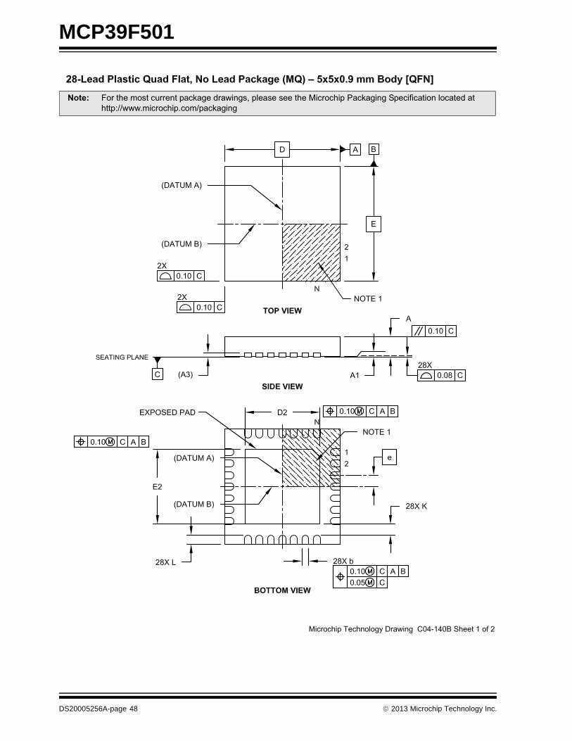
MCP39F501
Note: For the most current package drawings, please see the Microchip Packaging Specification located at http://www.microchip.com/packaging
DS20005256A-page 48 2013 Microchip Technology Inc.
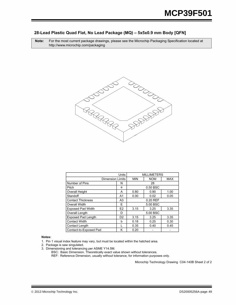
MCP39F501
Note: For the most current package drawings, please see the Microchip Packaging Specification located at http://www.microchip.com/packaging
2013 Microchip Technology Inc. DS20005256A-page 49
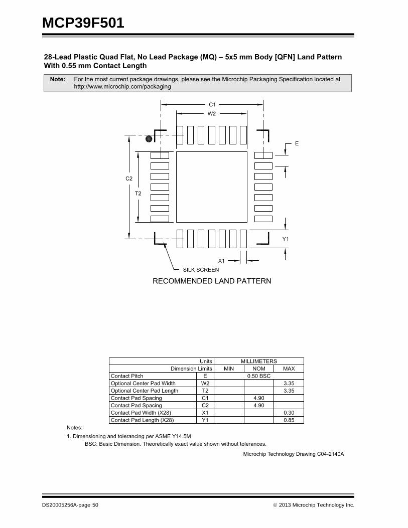
MCP39F501
28-Lead Plastic Quad Flat, No Lead Package (MQ) – 5x5 mm Body [QFN] Land PatternWith 0.55 mm Contact Length
Note: For the most current package drawings, please see the Microchip Packaging Specification located at http://www.microchip.com/packaging
Microchip Technology Drawing C04-2140A
DS20005256A-page 50 2013 Microchip Technology Inc.
MCP39F501
APPENDIX A: REVISION HISTORY
Revision A (December 2013)
• Original Release of this Document.
2013 Microchip Technology Inc. DS20005256A-page 51

MCP39F501
NOTES:
DS20005256A-page 52 2013 Microchip Technology Inc.
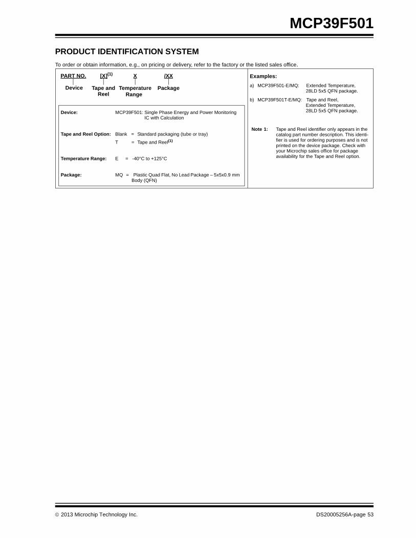
MCP39F501
PRODUCT IDENTIFICATION SYSTEM
To order or obtain information, e.g., on pricing or delivery, refer to the factory or the listed sales office.
Device: MCP39F501: Single Phase Energy and Power Monitoring IC with Calculation
Tape and Reel Option: Blank = Standard packaging (tube or tray)
T = Tape and Reel(1)
Temperature Range: E = -40°C to +125°C
Package: MQ = Plastic Quad Flat, No Lead Package – 5x5x0.9 mm Body (QFN)
Examples:
a) MCP39F501-E/MQ: Extended Temperature,28LD 5x5 QFN package.
b) MCP39F501T-E/MQ: Tape and Reel,Extended Temperature,28LD 5x5 QFN package.
PART NO. X
TemperatureRange
Device
/XX
Package
[X](1)
Tape andReel
Note 1: Tape and Reel identifier only appears in the catalog part number description. This identi-fier is used for ordering purposes and is not printed on the device package. Check with your Microchip sales office for package availability for the Tape and Reel option.
2013 Microchip Technology Inc. DS20005256A-page 53

MCP39F501
NOTES:
2013 Microchip Technology Inc. DS20005256A-page 54
Note the following details of the code protection feature on Microchip devices:
• Microchip products meet the specification contained in their particular Microchip Data Sheet.
• Microchip believes that its family of products is one of the most secure families of its kind on the market today, when used in the intended manner and under normal conditions.
• There are dishonest and possibly illegal methods used to breach the code protection feature. All of these methods, to our knowledge, require using the Microchip products in a manner outside the operating specifications contained in Microchip’s Data Sheets. Most likely, the person doing so is engaged in theft of intellectual property.
• Microchip is willing to work with the customer who is concerned about the integrity of their code.
• Neither Microchip nor any other semiconductor manufacturer can guarantee the security of their code. Code protection does not mean that we are guaranteeing the product as “unbreakable.”
Code protection is constantly evolving. We at Microchip are committed to continuously improving the code protection features of ourproducts. Attempts to break Microchip’s code protection feature may be a violation of the Digital Millennium Copyright Act. If such actsallow unauthorized access to your software or other copyrighted work, you may have a right to sue for relief under that Act.
Information contained in this publication regarding deviceapplications and the like is provided only for your convenienceand may be superseded by updates. It is your responsibility toensure that your application meets with your specifications.MICROCHIP MAKES NO REPRESENTATIONS ORWARRANTIES OF ANY KIND WHETHER EXPRESS ORIMPLIED, WRITTEN OR ORAL, STATUTORY OROTHERWISE, RELATED TO THE INFORMATION,INCLUDING BUT NOT LIMITED TO ITS CONDITION,QUALITY, PERFORMANCE, MERCHANTABILITY ORFITNESS FOR PURPOSE. Microchip disclaims all liabilityarising from this information and its use. Use of Microchipdevices in life support and/or safety applications is entirely atthe buyer’s risk, and the buyer agrees to defend, indemnify andhold harmless Microchip from any and all damages, claims,suits, or expenses resulting from such use. No licenses areconveyed, implicitly or otherwise, under any Microchipintellectual property rights.
2013 Microchip Technology Inc.
QUALITY MANAGEMENT SYSTEM CERTIFIED BY DNV
== ISO/TS 16949 ==
Trademarks
The Microchip name and logo, the Microchip logo, dsPIC, FlashFlex, KEELOQ, KEELOQ logo, MPLAB, PIC, PICmicro, PICSTART, PIC32 logo, rfPIC, SST, SST Logo, SuperFlash and UNI/O are registered trademarks of Microchip Technology Incorporated in the U.S.A. and other countries.
FilterLab, Hampshire, HI-TECH C, Linear Active Thermistor, MTP, SEEVAL and The Embedded Control Solutions Company are registered trademarks of Microchip Technology Incorporated in the U.S.A.
Silicon Storage Technology is a registered trademark of Microchip Technology Inc. in other countries.
Analog-for-the-Digital Age, Application Maestro, BodyCom, chipKIT, chipKIT logo, CodeGuard, dsPICDEM, dsPICDEM.net, dsPICworks, dsSPEAK, ECAN, ECONOMONITOR, FanSense, HI-TIDE, In-Circuit Serial Programming, ICSP, Mindi, MiWi, MPASM, MPF, MPLAB Certified logo, MPLIB, MPLINK, mTouch, Omniscient Code Generation, PICC, PICC-18, PICDEM, PICDEM.net, PICkit, PICtail, REAL ICE, rfLAB, Select Mode, SQI, Serial Quad I/O, Total Endurance, TSHARC, UniWinDriver, WiperLock, ZENA and Z-Scale are trademarks of Microchip Technology Incorporated in the U.S.A. and other countries.
SQTP is a service mark of Microchip Technology Incorporated in the U.S.A.
GestIC and ULPP are registered trademarks of Microchip Technology Germany II GmbH & Co. KG, a subsidiary of Microchip Technology Inc., in other countries.
All other trademarks mentioned herein are property of their respective companies.
© 2013, Microchip Technology Incorporated, Printed in the U.S.A., All Rights Reserved.
Printed on recycled paper.
ISBN: 9781620777787
Microchip received ISO/TS-16949:2009 certification for its worldwide
DS20005256A-page 55
headquarters, design and wafer fabrication facilities in Chandler and Tempe, Arizona; Gresham, Oregon and design centers in California and India. The Company’s quality system processes and procedures are for its PIC® MCUs and dsPIC® DSCs, KEELOQ® code hopping devices, Serial EEPROMs, microperipherals, nonvolatile memory and analog products. In addition, Microchip’s quality system for the design and manufacture of development systems is ISO 9001:2000 certified.

DS20005256A-page 56 2013 Microchip Technology Inc.
AMERICASCorporate Office2355 West Chandler Blvd.Chandler, AZ 85224-6199Tel: 480-792-7200 Fax: 480-792-7277Technical Support: http://www.microchip.com/supportWeb Address: www.microchip.com
AtlantaDuluth, GA Tel: 678-957-9614 Fax: 678-957-1455
BostonWestborough, MA Tel: 774-760-0087 Fax: 774-760-0088
ChicagoItasca, IL Tel: 630-285-0071 Fax: 630-285-0075
ClevelandIndependence, OH Tel: 216-447-0464 Fax: 216-447-0643
DallasAddison, TX Tel: 972-818-7423 Fax: 972-818-2924
DetroitFarmington Hills, MI Tel: 248-538-2250Fax: 248-538-2260
IndianapolisNoblesville, IN Tel: 317-773-8323Fax: 317-773-5453
Los AngelesMission Viejo, CA Tel: 949-462-9523 Fax: 949-462-9608
Santa ClaraSanta Clara, CA Tel: 408-961-6444Fax: 408-961-6445
TorontoMississauga, Ontario, CanadaTel: 905-673-0699 Fax: 905-673-6509
ASIA/PACIFICAsia Pacific OfficeSuites 3707-14, 37th FloorTower 6, The GatewayHarbour City, KowloonHong KongTel: 852-2401-1200Fax: 852-2401-3431
Australia - SydneyTel: 61-2-9868-6733Fax: 61-2-9868-6755
China - BeijingTel: 86-10-8569-7000 Fax: 86-10-8528-2104
China - ChengduTel: 86-28-8665-5511Fax: 86-28-8665-7889
China - ChongqingTel: 86-23-8980-9588Fax: 86-23-8980-9500
China - HangzhouTel: 86-571-2819-3187 Fax: 86-571-2819-3189
China - Hong Kong SARTel: 852-2943-5100 Fax: 852-2401-3431
China - NanjingTel: 86-25-8473-2460Fax: 86-25-8473-2470
China - QingdaoTel: 86-532-8502-7355Fax: 86-532-8502-7205
China - ShanghaiTel: 86-21-5407-5533 Fax: 86-21-5407-5066
China - ShenyangTel: 86-24-2334-2829Fax: 86-24-2334-2393
China - ShenzhenTel: 86-755-8864-2200 Fax: 86-755-8203-1760
China - WuhanTel: 86-27-5980-5300Fax: 86-27-5980-5118
China - XianTel: 86-29-8833-7252Fax: 86-29-8833-7256
China - XiamenTel: 86-592-2388138 Fax: 86-592-2388130
China - ZhuhaiTel: 86-756-3210040 Fax: 86-756-3210049
ASIA/PACIFICIndia - BangaloreTel: 91-80-3090-4444 Fax: 91-80-3090-4123
India - New DelhiTel: 91-11-4160-8631Fax: 91-11-4160-8632
India - PuneTel: 91-20-3019-1500
Japan - OsakaTel: 81-6-6152-7160 Fax: 81-6-6152-9310
Japan - TokyoTel: 81-3-6880- 3770 Fax: 81-3-6880-3771
Korea - DaeguTel: 82-53-744-4301Fax: 82-53-744-4302
Korea - SeoulTel: 82-2-554-7200Fax: 82-2-558-5932 or 82-2-558-5934
Malaysia - Kuala LumpurTel: 60-3-6201-9857Fax: 60-3-6201-9859
Malaysia - PenangTel: 60-4-227-8870Fax: 60-4-227-4068
Philippines - ManilaTel: 63-2-634-9065Fax: 63-2-634-9069
SingaporeTel: 65-6334-8870Fax: 65-6334-8850
Taiwan - Hsin ChuTel: 886-3-5778-366Fax: 886-3-5770-955
Taiwan - KaohsiungTel: 886-7-213-7828Fax: 886-7-330-9305
Taiwan - TaipeiTel: 886-2-2508-8600 Fax: 886-2-2508-0102
Thailand - BangkokTel: 66-2-694-1351Fax: 66-2-694-1350
EUROPEAustria - WelsTel: 43-7242-2244-39Fax: 43-7242-2244-393Denmark - CopenhagenTel: 45-4450-2828 Fax: 45-4485-2829
France - ParisTel: 33-1-69-53-63-20 Fax: 33-1-69-30-90-79
Germany - MunichTel: 49-89-627-144-0 Fax: 49-89-627-144-44
Italy - Milan Tel: 39-0331-742611 Fax: 39-0331-466781
Netherlands - DrunenTel: 31-416-690399 Fax: 31-416-690340
Spain - MadridTel: 34-91-708-08-90Fax: 34-91-708-08-91
UK - WokinghamTel: 44-118-921-5869Fax: 44-118-921-5820
Worldwide Sales and Service
08/20/13