Embed Size (px)
DESCRIPTION
MCS-012: Computer Organization and Assembly Language Programming - Block-1
Citation preview


Indira Gandhi National Open University School of Computer & Information Sciences
MCS-012 COMPUTER
ORGANISATION & ASSEMBLY
LANGUAGE PROGRAMMING
Block
1 INTRODUCTION TO DIGITAL CIRCUITS
UNIT 1
The Basic Computer 5 UNIT 2 Data Representation 31 UNIT 3 The Principles Of Logic Circuits I 60
UNIT 4
The Principles Of Logic Circuits II 87

Programme / Course Design Committee
Prof. Sanjeev K. Aggarwal, IIT, Kanpur Prof. M. Balakrishnan, IIT , Delhi Prof. Harish Karnick, IIT, Kanpur Prof. C. Pandurangan, IIT, Madras Dr. Om Vikas, Sr. Director, MIT Prof. P. S. Grover, Sr. Consultant, SOCIS, IGNOU
Faculty of School of Computer and Information Sciences Shri Shashi Bhushan Shri Akshay Kumar Prof. Manohar Lal Shri V.V. Subrahmanyam Shri P.Venkata Suresh
Block Preparation Team
Dr. MPS Bhatia (Content Editor) Mr. Niranjan Sinha (NSIT), New Delhi (Language Editor)
Ms. Suman Madan SS College of Business Studies, DU New Delhi
Mr. Akshay Kumar SOCIS, IGNOU
Course Coordinator: Shri Akshay Kumar
Block Production Team Shri H.K. Som, SOCIS
August, 2004 ©Indira Gandhi National Open University, 2004
ISBN—81-266-1385-8 All rights reserved. No part of this work may be reproduced in any form, by mimeograph or any other means, without permission in writing from the Indira Gandhi National Open University. Further information on the Indira Gandhi National Open University courses may be obtained from the University’s office at Maidan Garhi, New Delhi-110068. Printed and published on behalf of the Indira Gandhi National Open University, New Delhi by the Director, SOCIS.

COURSE INTRODUCTION
In the modern era, Computer system is used in most aspects of life. You may use many different types of software on a computer system for particular applications ranging from simple document creation to space data processing. But, how does a Software is executed by the Computer Hardware? The answer to this basic question is contained in this Course. This course presents an overview of the Computer hardware, (which include discussion on topics like digital electronic circuits, various storage devices such as hard disk, optical storage, display and other input/output technologies) and computer organization and architecture (which includes the basic components of computer that help it in execution of programs/ applications). Since, personal Computer is one of the major technology of the present, we will use it as an example for discussion, however, the examples are not just limited to personal computers only. Thus, after going through this course, you not only will acquire the conceptual framework of Computer Organisation and Architecture but also would be able to use the concepts in the domain of Personal Computers. This course includes details on data representation, interconnection structures, memory system, input-output system, and the Central Processing Unit. It also provides a detailed view of digital logic circuits, microprocessors and assembly language Programming and some of the important peripheral devices. You must attempt various assembly programs during the lab course in which practical sessions have been allocated for assembly language. You are also advised to write some sample programs in assembly and test them logically. The course is divided into four blocks.
The first block deals with the introduction of computer and its components, History of Computers, Data Representation, Instruction Execution, Interrupts, Buses, Boolean Algebra, Design of Logic Circuits, etc.
The second block deals with the Memory System, The Memory Hierarchy, Secondary Storage technologies, the concepts of high speed memory, Cache Organisation, the Memory System of Micro-Computers, Input/ Output System, The Input Output interfaces, Input Output techniques, DMA, Input Output processors, External Communication Interfaces, Interrupt Processing, BUS arbitration, etc.
The third block deals with the Central Processing Unit. It includes the Instruction Set, the Instruction format, the Instruction Set Architecture, Micro-operations, the organization of Arithmetic logic unit, Design of simple units of ALU, the Control Unit, The hardwired control, Wilkes control, the Micro-programmed control etc.
The fourth block deals with the Assembly Language Programming, the Microprocessor, the Instruction format of 8086 Microprocessor, the addressing modes, Input output in Assembly Language Program, the Assembly Programming tools, Sample Assembly Programs including arrays, counters, dealing with various simple statements, use of various addressing modes, Modular Programming, Interfacing assembly with HLL, Device drivers in assembly, Interrupts in assembly etc.

BLOCK INTRODUCTION
The first block introduces you about the concepts of Computer Organisation. It covers the data representation and digital logic circuits in details. The block is divided into four units. Unit 1 covers the basic computer Organisation. It deal with the von Neumann Architecture, History of Computers, the Instruction Execution and Interrupt, and concept of BUS.
Unit 2 deals with the Data Representation. It includes the Number Systems such as Binary, Decimal, Octal, Hexadecimal, Conversion of Representation, Alphanumeric representation, Fixed Point Representation, Floating point representation, Arithmetic operations on binary numbers, BCD representation, Error detection and correction codes, Boolean Algebraic operations etc.
Unit 3 introduces the students to the basic logic circuits. It deals with Logic Gates, Logic circuits, Design of Combinational and various examples of logic combinational circuits such as Adders, Decoders, Multiplexers, Encoders, ROM etc.
Unit 4 provides details on the Sequential circuits, Flip flops, Excitation tables, Edge triggered, Master-Slave flip flops, Sequential circuit design, examples of sequential circuits such as Counters, Registers, RAM, etc.
A course on computers can never be complete because of the existing diversities of the computer systems. Therefore, you are advised to read through further readings to enhance the basic understanding you will acquire from the block.
Further Readings For The Block
1) Stallings W., Computer Organization & Architecture: Designing For Performance, 6th Edition, Prentice Hall of India Publication, 2002/ Pearson Education Asia 2003
2) Mano M Morris, Computer System Architecture, 3rd Edition, Prentice Hall of India Publication, 2001 / Pearson Education Asia 2003
3) Hennessy/Patterson, Computer Architecture: A Quantitative. Approach; 3rd Edition, Morgan Kaufmann, 2003.

5
The Basic Computer
UNIT 1 THE BASIC COMPUTER
Structure Page Nos. 1.0 Introduction 5 1.1 Objectives 5 1.2 The von Neumann Architecture 5 1.3 Instruction Execution: An Example 9 1.4 Instruction Cycle 12 1.4.1 Interrupts 1.4.2 Interrupts and Instruction Cycle 1.5 Computers: Then and Now 18 1.5.1 The Beginning 1.5.2 First Generation Computers 1.5.3 Second Generation Computers 1.5.4 Third Generation Computers 1.5.5 Later Generations 1.6 Summary 29 1.7 Solutions/Answers 29
1.0 INTRODUCTION
The use of Information Technology (IT) is well recognised. IT has become a must for the survival of all business houses with the growing information technology trends. Computer is the main component of an Information Technology network. Today, computer technology has permeated every sphere of existence of modern man. From railway reservations to medical diagnosis, from TV programmes to satellite launching, from matchmaking to criminal catching ─ everywhere we witness the elegance, sophistication and efficiency possible only with the help of computers. In this unit, you will be introduced to one of the important computer system structures: the von Neumann Architecture. In addition, you will be introduced to the concepts of a simple model of Instruction execution. This model will be enhanced in the later blocks of this course. More details on these terms can be obtained from further reading. We have also discussed about the main developments during the various periods of computer history. Finally, we will discuss about the basic components of microprocessors and their uses.
1.1 OBJECTIVES
After going through this unit you will be able to:
• define the logical structure of the computer; • define the instruction cycle; • define the concept or Interrupt; • discuss the basic features of computers; and • define the various components of a modern computer and their usage.
1.2 THE VON NEUMANN ARCHITECTURE
The von Neumann architecture was the first major proposed structure for a general-purpose computer. However, before describing the main components of von Neumann

6
Introduction to Digital Circuits
architecture, let us first define the term ‘computer’ as this will help us in discussing about von Neumann architecture in logical detail.
Computer is defined in the Oxford dictionary as “An automatic electronic apparatus for making calculations or controlling operations that are expressible in numerical or logical terms”.
The definition clearly categorises computer as an electronic apparatus although the first computers were mechanical and electro-mechanical apparatuses. The definition also points towards the two major areas of computer applications viz., data processing’s and computer assisted controls/operations. Another important aspect of the definition is the fact that the computer can perform only those operations/ calculations, which can be expressed in Logical or Numerical terms.
Some of the basic questions that arise from above definition are: How are the data processing and control operations performed by an electronic device like the computer?
Well, electronic components are used for creating basic logic circuits that are used to perform calculations. These components are further discussed in the later units. However, for the present discussion, it would be sufficient to say that there must be a certain unit that will perform the task of data processing and control.
What is the basic function performed by a computer? The basic function performed by a computer is the execution of the program. A program is a sequence of instructions, which operates on data, to perform certain tasks such as finding a prime number. The computer controls the execution of the program.
What is data in computers? In modern digital computers data is represented in binary form by using two symbols 0 and 1. These are called binary digits or bits. But the data which we deal with consists of numeric data and characters such as decimal digits 0 to 9, alphabets A to Z, arithmetic operators (e.g. +,-, etc.), relations operators (e.g. =, > , etc.), and many other special characters (e.g.;,@,{,], etc.). Therefore, there has to be a mechanism for data representation. Old computers use eight bits to represent a character. This allows up to 28 = 256 different items to be represented uniquely. This collection of eight bits is called a byte. Thus, one byte is used to represent one character internally. Most computers use two bytes or four bytes to represent numbers (positive and negative) internally. The data also includes the operational data such as integer, decimal number etc. We will discuss more about data representation in the next unit.
Thus, the prime task of a computer is to perform instruction execution. The key questions, which can be asked in this respect, are: (a) how are the instructions supplied to the computer? and (b) how are the instructions interpreted and executed?
Let us answer the second question first. All computers have a Unit that performs the arithmetic and logical functions. This Unit is referred to as the Arithmetic Logic Unit (ALU). But how will the computer determine what operation is to be performed by ALU or in other words who will interpret the operation that is to be performed by ALU?
This interpretation is done by the Control Unit of the computer. The control unit accepts the binary form of instruction and interprets the instruction to generate control signals. These control signals then direct the ALU to perform a specified arithmetic or logic function on the data. Therefore, by changing the control signal the desired function can be performed on data. Or conversely, the operations that need to be performed on the data can be obtained by providing a set of control signals. Thus, for a new operation one only needs to change the set of control signals.
The unit that interprets a code (a machine instruction) to generate respective control signals is termed as Control Unit (CU). A program now consists of a sequence of codes. Each code is, in effect, an instruction, for the computer. The hardware

7
The Basic Computer interprets each of these instructions and generates respective control signals such that the desired operation is performed on the data.
The Arithmetic Logic Unit (ALU) and the Control Unit (CU) together are termed as the Central Processing Unit (CPU). The CPU is the most important component of a computer’s hardware.
All these arithmetic and logical Operations are performed in the CPU in special storage areas called registers. The size of the register is one of the important considerations in determining the processing capabilities of the CPU. Register size refers to the amount of information that can be held in a register at a time for processing. The larger the register size, the faster may be the speed of processing.
But, how can the instructions and data be put into the computers? The instructions and data to a computer are supplied by external environment; it implies that input devices are needed in the computer. The main responsibility of input devices will be to put the data in the form of signals that can be recognised by the system. Similarly, we need another component, which will report the results in proper format. This component is called output device. These components together are referred to as input/output (I/O) devices.
In addition, to transfer the information, the computer system internally needs the system interconnections. At present we will not discuss about Input/Output devices and system interconnections in details, except the information that most common input/output devices are keyboard, monitor and printer, and the most common interconnection structure is the Bus structure. These concepts are detailed in the later blocks.
Input devices can bring instructions or data only sequentially, however, a program may not be executed sequentially as jump, looping, decision-making instructions are normally encountered in programming. In addition, more than one data element may be required at a time. Therefore, a temporary storage area is needed in a computer to store temporarily the instructions and the data. This component is referred to as memory.
The memory unit stores all the information in a group of memory cells such as a group of 8 binary digits (that is a byte) or 16 bits or 32 bits etc. These groups of memory cells or bits are called memory locations. Each memory location has a unique address and can be addressed independently. The contents of the desired memory locations are provided to the CPU by referring to the address of the memory location. The amount of information that can be held in the main memory is known as memory capacity. The capacity of the main memory is measured in Mega Bytes (MB) or Giga Bytes (GB). One-kilo byte stands for 210 bytes, which are 1024 bytes (or approximately 1000 bytes). A Mega byte stands for 220 bytes, which is approximately a little over one million bytes, a giga byte is 230 bytes.
Let us now define the key features of von Neumann Architecture:
• The most basic function performed by a computer is the execution of a program, which involves:
the execution of an instruction, which supplies the information about an operation, and
the data on which the operation is to be performed. The control unit (CU) interprets each of these instructions and generates respective control signals.
• The Arithmetic Logic Unit (ALU) performs the arithmetic and logical Operations in special storage areas called registers as per the instructions of
control unit. The size of the register is one of the important considerations in determining the processing capabilities of the CPU. Register size refers to the

8
Introduction to Digital Circuits
amount of information that can be held in a register at a time for processing. The larger the register size, the faster may be the speed of processing.
• An Input/ Output system involving I/O devices allows data input and reporting of the results in proper form and format. For transfer of information a computer system internally needs the system interconnections. One such interconnection structure is BUS interconnection.
• Main Memory is needed in a computer to store instructions and the data at the time of Program execution. Memory to CPU is an important data transfer path. The amount of information, which can be transferred between CPU and memory, depends on the size of BUS connecting the two.
• It was pointed out by von-Neumann that the same memory can be used for Storing data and instructions. In such a case the data can be treated as data on which processing can be performed, while instructions can be treated as data, which can be used for the generation of control signals.
• The von Neumann machine uses stored program concept, i.e., the program and data are stored in the same memory unit for execution. The computers prior to this idea used to store programs and data on separate memories. Entering and modifying these programs was very difficult as they were entered manually by setting switches, plugging, and unplugging.
• Execution of instructions in von Neumann machine is carried out in a sequential fashion (unless explicitly altered by the program itself) from one instruction to the next.
Figure 1 shows the basic structure of a conventional von Neumann machine
Figure 1: Structure of a Computer
A von Neumann machine hcontrol unit (CU). This feaSeveral other architecturesabout non von Neumann ar
Check Your Progress 1
1) State True or False
a) A byte is equal to 8 b
b) von Neumann archite instructions. The me the memory, which s
c) In von Neumann arc independently. d) A program is a seque
as only a single path between the main memory and ture/constraint is referred to as von Neumann bottleneck. have been suggested for modern computers. You can know chitectures in further readings.
its and can represent a character internally.
cture specifies different memory for data and mory, which stores data, is called data memory and tores instructions, is called instruction memory.
hitecture each bit of memory can be accessed
nce of instructions designed for achieving a task/goal.
T/F

The Basic Computer e) One MB is equal to 1024KB.
f) von Neumann machine has one path between memory and control unit.
This is the bottleneck of von Neumann machines.
2) What is von Neumann Architecture? …………………………………………………………………………………………
…………………………………………………………………………………………
…………………………………………………………………………………………
3) Why is memory needed in a computer?
………………………………………………… ………………………………………
…………………………………………………………………………………………
…………………………………………………………………………………………
1.3 INSTRUCTION EXECUTION: AN EXAMPL
After discussing about the basic structure of the computer, let us now try to answebasic question: “How does the Computer execute a Program?” Let us explain this the help of an example from higher level language domain.
Problem: Write a program to add two numbers.
A sample C program (Assuming two fixed values of numbers as a = 5 and b = 2)
1. #include <stdio.h>
2. main ()
3. {4. int a =5, b=2, c;
5. c= a+b;
6. printf (“\n The added value is: % d”, c);
7. } The program at line 4 declares variables that will be equivalent to 3 memory locatinamely a, b and c. At line 5 these variables are added and at line 6 the value of c iprinted. But, how will these instructions be executed by CPU?
First you need to compile this program to convert it to machine language. But howwill the machine instructions look like?
Let us assume a hypothetical instruction set of a machines of a size of 16 binary di(bits) instructions and data. Each instruction of the machine consists of two components: (a) Operation code that specifies the operation that is to be performedthe instruction, and (b) Address of the operand in memory on which the given operation is to be performed.
Let us further assume that the size of operation code is assumed to be of six bits; therefore, rest 10 bits are for the address of the operand. Also the memory word siis assumed to be of 16 bits. Figure 2 shows the instruction and data formats for thimachine. However, to simplify our discussion, let us present the operation code uPnemonics like LOAD, ADD, STORE and decimal values of operand addresses ansigned decimal values for data.
9
.
.
E
r the with
ons s
gits
by
ze s sing d

10
Introduction to Digital Circuits
Figure 2: Instruction and data format of an assumed machine
The instruction execution is performed in the CPU registers. But before we define the process of instruction execution let us first give details on Registers, the temporary storage location in CPU for program execution. Let us define the minimum set of registers required for von Neumann machines:
Accumulator Register (AC): This register is used to store data temporarily for computation by ALU. AC is considered to contain one of the operands. The result of computation by ALU is also stored back to AC. It implies that the operand value is over-written by the result.
Memory Address Register (MAR): It specifies the address of memory location from which data or instruction is to be accessed (read operation) or to which the data is to be stored (write operation). Refer to figure 3.
Memory Buffer Register (MBR): It is a register, which contains the data to be written in the memory (write operation) or it receives the data from the memory (read operation).
Program Counter (PC): It keeps track of the instruction that is to be executed next, that is, after the execution of an on-going instruction.
Instruction Register (IR): Here the instructions are loaded prior to execution.
Comments on figure 3 are as follows:
• All representation are in decimals. (In actual machines the representations are in Binary). • The Number of Memory Locations = 16 • Size of each memory location = 16 bits = 2 Bytes (Compare with contemporary machines word size of 16,32, 64 bits) • Thus, size of this sample memory = 16 words (Compare it with actual memory) size, which is 128 MB, 256 MB, 512 MB, or more). • In the diagram MAR is pointing to location 10. • The last operation performed was “read memory location 10” which is 65 in this. Thus, the contents of MBR is also 65.
Figure 3: CPU registers and their functions

11
The Basic Computer The role of PC and IR will be explained later.
Now let us define several operation codes required for this machine, so that we can translate the High level language instructions to assembly/machine instructions.
Operation Code
Definition/Operation (please note that the address part in the Instruction format specifies the Location of the Operand on whom operation is to be performed
LOAD as “Load the accumulator with the content of memory” STORE as “Store the current value of Accumulator in the
memory” ADD as “Add the value from memory to the Accumulator”
A sample machine instructions for the assumed system for line 5 that is c = a + b in the program would be:
LOAD A ; Load the contents of memory location A to Accumulator register
ADD B ; Add the contents of B to contents of Accumulator and store result in Accumulator.
STORE C ; Store the content into location C
Please note that a simple one line statement in ‘C’ program has been translated to three machine instructions as above. Please also note that these translated instructions are machine dependent.
Now, how will these instructions execute?
Let us assume that the above machine instructions are stored in three consecutive memory locations 1, 2 and 3 and the PC contains a value (1), which in turn is address of first of these instructions. (Please refer to figure 4 (a)).
Figure 4: Memory and Registers Content on execution or the three given Consecutive Instructions (All notations in Decimals)
Then the execution of the instructions will be as follows:
Fetch First Instruction into CPU:
Step 1: Find or calculate the address of the first instruction in memory: In this machine example, the next instruction address is contained in PC register. It contains 1, which is the address of first instruction to be executed. (figure 4 a).
Step 2: Bring the binary instruction to IR register. This step requires:
• Passing the content of PC to Memory Address Registers so that the instruction pointed to by PC is fetched. That is location 1’s content is fetched. • CPU issues “Memory read” operation, thus, brings contents of location pointed by MAR (1 in this case) to the MBR register. • Content of MBR is transferred to IR. In addition PC is incremented to point to next instruction in sequence (2 in this case).

12
Introduction to Digital Circuits
Execute the Instruction
Step 3: The IR has the instruction LOAD A, which is decoded as “Load the content of address A in the accumulator register”.
Step 4: The address of operand that is 13, that is A, is transferred to MAR register. Step 5: The content of memory location (specified by MAR that is location 13) is transferred to MBR. Step 6: The content of MBR is transferred to Accumulator Register.
Thus, the accumulator register is loaded with the content of location A, which is 5. Now the instruction 1 execution is complete, and the next instruction that is 2 (indicated by PC) is fetched and PC is incremented to 3. This instruction is ADD B, which instruct CPU to add the contents of memory location B to the accumulator. On execution of this instruction the accumulator will contain the sum of its earlier value that is A and the value stored in memory location B.
On execution of the instruction at memory location 3, PC becomes 4; the accumulator results are stored in location C, that is 15, and IR still contains the third instruction. This state is shown in figure 4 (C).
Please note that the execution of the instructions in the above example is quite simple and requires only data transfer and data processing operations in each instruction. Also these instructions require one memory reference during its execution.
Some of the problems/limitations of the example shown above are?
1. The size of memory shown in 16 words, whereas, the instruction is capable of addressing 210 =1 K words of Memory. But why 210 , because 10 bits are reserved for address in the machine instruction format.
2. The instructions shown are sequential in nature, however, a machine instruction can also be a branch instruction that causes change in the sequence of instruction execution.
3. When does the CPU stop executing a program? A program execution is normally completed at the end of a program or it can be terminated due to an error in program execution or sometimes all running programs will be terminated due to catastrophic failures such as power failure.
1.4 INSTRUCTION CYCLE
We have discussed the instruction execution in the previous section, now let us discuss more about various types of instruction execution.
What are the various types of operations that may be required by computer for execution of instruction? The following are the possible steps:
S.No. Step to be performed How is it done Who does it
1 Calculate the address of next instruction to be executed
The Program Counter (PC register stores the address of next instruction.
Control Unit (CU).
2. Get the instruction in the CPU register
The memory is accessed and the desired instruction is brought to register (IR) in CPU
Memory Read operation is done. Size of instruction is important. In addition, PC is incremented to point to next instruction in sequence.
3. Decode the instruction
The control Unit issues necessary control signals
CU.

13
The Basic Computer 4. Evaluate the operand
address CPU evaluates the address based on the addressing mode specified.
CPU under the control of CU
5. Fetch the operand
The memory is accessed and the desired operands brought into the CPU Registers
Memory Read
Repeat steps 4 and 5 if instruction has more than one operands. 6. Perform the operation
as decoded in steps3.
The ALU does evaluation of arithmetic or logic, instruction or the transfer of control operations.
ALU/CU
7. Store the results in memory
The value is written to desired memory location
Memory write
Figure 5: Instruction Cycle

14
Introduction to Digital Circuits
Thus, in general, the execution cycle for a particular instruction may involve more than one stage and memory references. In addition, an instruction may ask for an I/O operation. Considering the steps above, let us work out a more detailed view of instruction cycle. Figure 5 gives a diagram of an instruction cycle.
Please note that in the preceding diagram some steps may be bypassed while some may be visited more than once. The instruction cycle shown in figure 5 consists of following states/stages:
• First the address of the next instruction is calculated, based on the size of instruction and memory organisation. For example, if in a computer an instruction is of 16 bits and if memory is organized as 16-bits words, then the address of the next instruction is evaluated by adding one in the address of the current instruction. In case, the memory is organized as bytes, which can be addressed individually, then we need to add two in the current instruction address to get the address of the next instruction to be executed in sequence. • Now, the next instruction is fetched from a memory location to the CPU registers such as Instruction register. • The next state decodes the instruction to determine the type of operation desired and the operands to be used. • In case the operands need to be fetched from memory or via Input devices, then the address of the memory location or Input device is calculated. • Next, the operand is fetched (or operands are fetched one by one) from the memory or read from the Input devices. • Now, the operation, asked by the instruction is performed. • Finally, the results are written back to memory or Output devices, wherever desired by first calculating the address of the operand and then transferring the values to desired destination.
Please note that multiple operands and multiple results are allowed in many computers. An example of such a case may be an instruction ADD A, B. This instruction requires operand A and B to be fetched.
In certain machines a single instruction can trigger an operation to be performed on an array of numbers or a string of characters. Such an operation involves repeated fetch for the operands without fetching the instruction again, that is, the instruction cycle loops at operand fetch.
Thus, a Program is executed as per the instruction cycle of figure 5. But what happens when you want the program to terminate in between? At what point of time is an interruption to a program execution allowed? To answer these questions, let us discuss the process used in computer that is called interrupt handling.
1.4.1 Interrupts
The term interrupt is an exceptional event that causes CPU to temporarily transfer its control from currently executing program to a different program which provides service to the exceptional event. It is like you asking a question in a class. When you ask a question in a class by raising hands, the teacher who is explaining some point may respond to your request only after completion of his/her point. Similarly, an interrupt is acknowledged by the CPU when it has completed the currently executing instruction. An interrupt may be generated by a number of sources, which may be either internal or external to the CPU.

15
The Basic Computer Some of the basic issues of interrupt are:
• What are the different kinds of interrupts?
• What are the advantages of having an interruption mechanism?
• How is the CPU informed about the occurrence of an interrupt?
• What does the CPU do on occurrence of an interrupt?
Figure 6 Gives the list of some common interrupts and events that cause the occurrence of those interrupts.
Interrupt Condition Occurrence of Event
Interrupt are generated by executing program itself (also called traps)
Division by Zero The number exceeds the maximum
allowed.
Attempt of executing an illegal/privileged instruction.
Trying to reference memory location other than allowed for that program.
Interrupt generated by clock in the processor
Generally used on expiry of time allocated for a program, in multiprogramming operating systems.
Interrupts generated by I/O devices and their interfaces
Request of starting an Input/Output operation.
Normal completion of an Input/Output operation.
Occurrence of an error in Input/Output operation.
Interrupts on Hardware failure Power failure Memory parity error.
Figure 6: Various classes of Interrupts
Interrupts are a useful mechanism. They are useful in improving the efficiency of processing. How? This is to the fact that almost all the external devices are slower than the processor, therefore, in a typical system, a processor has to continually test whether an input value has arrived or a printout has been completed, in turn wasting a lot of CPU time. With the interrupt facility CPU is freed from the task of testing status of Input/Output devices and can do useful processing during this time, thus increasing the processing efficiency.
How does the CPU know that an interrupt has occurred? There needs to be a line or a register or status word in CPU that can be raised on occurrence of interrupt condition.
Once a CPU knows that an interrupt has occurred then what?
First the condition is to be checked as to why the interrupt has occurred. That includes not only the device but also why that device has raised the interrupt. Once the

16
Introduction to Digital Circuits
interrupt condition is determined the necessary program called ISRs (Interrupt servicing routines) must be executed such that the CPU can resume further operations.
For example, assume that the interrupt occurs due to an attempt by an executing program for execution of an illegal or privileged instruction, then ISR for such interrupt may terminate the execution of the program that has caused this condition. Thus, on occurrence of an Interrupt the related ISR is executed by the CPU. The ISRs are pre-defined programs written for specific interrupt conditions.
Considering these requirements let us work out the steps, which CPU must perform on the occurrence of an interrupt.
• The CPU must find out the source of the interrupt, as this will determine which interrupt service routine is to be executed. • The CPU then acquires the address of the interrupt service routine, which are stored in the memory (in general). • What happens to the program the CPU was executing before the interrupt? This
program needs to be interrupted till the CPU executes the Interrupt service program. Do we need to do something for this program? Well the context of this program is to be saved. We will discuss this a bit later.
• Finally, the CPU executes the interrupt service routine till the completion of the routine. A RETURN statement marks the end of this routine. After that, the control is passed back to the interrupted program.
Let us analyse some of the points above in greater detail.
Let us first discuss saving the context of a program. The execution of a program in the CPU is done using certain set of registers and their respective circuitry. As the CPU registers are also used for execution of the interrupt service routine, it is highly likely that these routines alter the content of several registers. Therefore, it is the responsibility of the operating system that before an interrupt service routine is executed the previous content of the CPU registers should be stored, such that the execution of interrupted program can be restarted without any change from the point of interruption. Therefore, at the beginning of interrupt processing the essential context of the processor is saved either into a special save area in main memory or into a stack. This context is restored when the interrupt service routine is finished, thus, the interrupted program execution can be restarted from the point of interruption.
1.4.2 Interrupts and Instruction Cycle
Let us summarise the interrupt process, on the occurrence of an interrupt, an interrupt request (in the form of a signal) is issued to the CPU. The CPU on receipt of interrupt request suspends the operation of the currently executing program, saves the context of the currently executing program and starts executing the program which services that interrupt request. This program is also known as interrupt handler. After the interrupting condition/ device has been serviced the execution of original program is resumed. Thus, an interrupt can be considered as the interruption of the execution of an ongoing user program. The execution of user program resumes as soon as the interrupt processing is completed. Therefore, the user program does not contain any code for interrupt handling. This job is to be performed by the processor and the operating system, which in turn are also responsible for suspending the execution of the user program, and later after interrupt handling, resumes the user program from the point of interruption.

17
The Basic Computer
Figure 7: Instruction Cycle with Interrupt Cycle
But when ca a user program execution be interrupted?
It will not be desirable to interrupt a program while an instruction is getting executed and is in a state like instruction decode. The most desirable place for program

18
Introduction to Digital Circuits
interruption would be when it has completed the previous instruction and is about to start a new instruction. Figure 7 shows instruction execution cycle with interrupt cycle, where the interrupt condition is acknowledged. Please note that even interrupt service routine is also a program and after acknowledging interrupt the next instruction executed through instruction cycle is the first instruction of interrupt servicing routine.
In the interrupt cycle, the responsibility of the CPU/Processor is to check whether any interrupts have occurred checking the presence of the interrupt signal. In case no interrupt needs service, the processor proceeds to the next instruction of the current program. In case an interrupt needs servicing then the interrupt is processed as per the following.
• Suspend the execution of current program and save its context. • Set the Program counter to the starting address of the interrupt service routine of the interrupt acknowledged. • The processor then executes the instructions in the interrupt-servicing program. The interrupt servicing programs are normally part of the operating system. • After completing the interrupt servicing program the CPU can resume the . program it has suspended in step 1 above.
Check Your Progress 2
1) State True or False
i) The value of PC will be incremented by 1 after fetching each instruction if the memory word is of one byte and an instruction is 16 bits long. ii) MAR and MBR both are needed to fetch the data /instruction from the memory. iii) A clock may generate an interrupt.
iv) Context switching is not desired before interrupt processing. v) In case multiple interrupts occur at the same time, then only one of the interrupt will be acknowledged and rest will be lost. 2) What is an interrupt?
....................................................................................................................................
....................................................................................................................................
....................................................................................................................................
………………………………………………………………………………………..
3) What happens on the occurrence of an interrupt?
....................................................................................................................................
....................................................................................................................................
....................................................................................................................................
…………………………………………………………………………………………
1.5 COMPUTERS: THEN AND NOW
Let us now discuss the history of computers because this will give the basic information about the technological development trends in computer in the past anits projections for the future. If we want to know about computers completely, then
T/F
.
.
.
.
.
.
d we

19
The Basic Computer must look at the history of computers and look into the details of various technological and intellectual breakthroughs. These are essential to give us the feel of how much work and effort has been done in the past to bring the computer to this shape. Our effort in this section will be to describe the conceptual breakthroughs in the past. The ancestors of modern age computer were the mechanical and electromechanical devices. This ancestry can be traced as far back as the 17th Century, when the first machine capable of performing four mathematical operations, viz. addition, subtraction, division and multiplication, appeared. In the subsequent subsection we present a very brief account of Mechanical Computers.
1.5.1 The Beginning
Blaise Pascal made the very first attempt towards automatic computing. He invented a device, which consisted of lots of gears and chains which used to perform repeated additions and subtractions. This device was called Pascaline. Later many attempts were made in this direction. Charles Babbage, the grandfather of the modern computer, had designed two computers:
The Difference Engine: It was based on the mathematical principle of finite differences and was used to solve calculations on large numbers using a formula. It was also used for solving the polynomial and trigonometric functions.
The Analytical Engine by Babbage: It was a general purpose-computing device, which could be used for performing any mathematical operation automatically. The basic features of this analytical engine were:
• It was a general-purpose programmable machine. • It had the provision of automatic sequence control, thus, enabling programs to alter its sequence of operations. • The provision of sign checking of result existed. • A mechanism for advancing or reversing of control card was permitted thus
enabling execution of any desired instruction. In other words, Babbage had devised the conditional and branching instructions. The Babbage’s machine was fundamentally the same as the modern computer. Unfortunately, Babbage work could not be completed. But as a tribute to Charles Babbage his Analytical Engine was completed in the last decade of the 20th century and is now on display at the Science Museum at London.
The next notable attempts towards computers were electromechanical. Zuse used electromechanical relays that could be either opened or closed automatically. Thus, the use of binary digits, rather than decimal numbers started, in computers. Harvard Mark-I and the Bug
The next significant effort towards devising an electromechanical computer was made at the Harvard University, jointly sponsored by IBM and the Department of UN Navy, Howard Aiken of Harvard University developed a system called Mark I in 1944. Mark I was a decimal machine, that is, the computations were performed using decimal digits.
Some of you must have heard a term called “bug”. It is mainly used to indicate errors in computer programs. This term was coined when one day, a program in Mark-I did not run properly due to a moth short-circuiting the computer. Since then, the moth or the bug has been linked with errors or problems in computer programming. Thus, the process of eliminating error in a program is known as ‘debugging’.
20
Introduction to Digital Circuits
The basic drawbacks of these mechanical and electromechanical computers were:
• Friction/inertia of moving components limited the speed. • The data movement using gears and liners was quite difficult and unreliable. • The change was to have a switching and storing mechanism with no moving parts. The electronic switching device “triode” vacuum tubes were used and
hence the first electronic computer was born. 1.5.2 First Generation Computers
It is indeed ironic that scientific inventions of great significance have often been linked with supporting a very sad and undesirable aspect of civilization, that is, fighting wars. Nuclear energy would not have been developed as fast, if colossal efforts were not spent towards devising nuclear bombs. Similarly, the origin of the first truly general-purpose computer was also designed to meet the requirement of World War II. The ENIAC (the Electronic Numerical Integrator And Calculator) was designed in 1945 at the University of Pennsylvania to calculate figures for thousands of gunnery tables required by the US army for accuracy in artillery fire. The ENIAC ushered in the era of what is known as first generation computers. It could perform 5000 additions or 500 multiplications per minute. It was, however, a monstrous installation. It used thousands of vacuum tubes (18000), weighed 30 tons, occupied a number of rooms, needed a great amount of electricity and emitted excessive heat.
The main features of ENIAC can be summarised as:
• ENIAC was a general purpose-computing machine in which vacuum tube technology was used. • ENIAC was based on decimal arithmetic rather than binary arithmetic. • ENIAC needed to be programmed manually by setting switches and plugging or
unplugging. Thus, to pass a set of instructions to the computer was difficult and time-consuming. This was considered to be the major deficiency of ENIAC.
The trends, which were encountered during the era of first generation computers were: • Centralised control in a single CPU; all the operations required a direct intervention of the CPU. • Use of ferrite-core main memory was started during this time. • Concepts such as use of virtual memory and index register (you will know more about these terms later) started. • Punched cards were used as input device. • Magnetic tapes and magnetic drums were used as secondary memory. • Binary code or machine language was used for programming. • Towards the end, due to difficulties encountered in use of machine language as programming language, the use of symbolic language that is now called assembly language started. • Assembler, a program that translates assembly language programs to machine language, was made. • Computer was accessible to only one programmer at a time (single user environment). • Advent of von-Neumann architecture. 1.5.3 Second Generation Computers
Silicon brought the advent of the second generation computers. A two state device called a transistor was made from silicon. Transistor was cheaper, smaller and dissipated less heat than vacuum tube, but could be utilised in a similar way to vacuum tubes. A transistor is called a solid state device as it is not created from wires, metal glass capsule and vacuum which was used in vacuum tubes. The transistors were invented in 1947 and launched the electronic revolution in 1950.

21
The Basic Computer But how do we characterise the future generation of computers?
The generations of computers are basically differentiated by the fundamental hardware technology. The advancement in technology led to greater speed, large memory capacity and smaller size in various generations. Thus, second generation computers were more advanced in terms of arithmetic and logic unit and control unit than their counterparts of the first generation and thus, computationally more powerful. On the software front at the same time use of high level languages started and the developments were made for creating better Operating System and other system software.
One of the main computer series during this time was the IBM 700 series. Each successful member of this series showed increased performance and capacity and reduced cost. In these series two main concepts, I/O channels - an independent processor for Input/Output, and Multiplexer - a useful routing device, were used. These two concepts are defined in the later units.
1.5.4 Third Generation Computers
The third generation has the basic hardware technology: the Integrated Circuits (ICs). But what are integrated circuits? Let us first define a term called discrete components. A single self-contained transistor is called discrete component. The discrete components such as transistors, capacitors, resistors were manufactured separately and were soldered on circuit boards, to create electronic components or computer cards. All these cards/components then were put together to make a computer. Since a computer can contain around 10,000 of these transistors, therefore, the entire mechanism was cumbersome. The basic idea of integrated circuit was to create electronic components and later the whole CPU on a single Integrated chip. This was made possible by the era of microelectronics (small electronics) with the invention of Integrated Circuits (ICs).
In an integrated circuit technology the components such as transistors, resistors and conductors are fabricated on a semiconductor material such as silicon. Thus, a desired circuit can be fabricated in a tiny piece of silicon. Since, the size of these components is very small in silicon, thus, hundreds or even thousands of transistors could be fabricated on a single wafer of silicon. These fabricated transistors are connected with a process of metalisation, thus, creating logic circuits on the chip.
Figure 8: Silicon Wafer, Chip and Gates

22
Introduction to Digital Circuits
An integrated circuit is constructed on a thin wafer of silicon, which is divided into a matrix of small areas (size of the order of a few millimeter squares). An identical circuit pattern is fabricated in a dust free environment on each of these areas and the wafer is converted into chips. (Refer figure 8). A chip consists of several gates, which are made using transistors. A chip also has a number of input and output connection points. A chip then is packaged separately in a housing to protect it. This housing provides a number of pins for connecting this chip with other devices or circuits. For example, if you see a microprocessor, what you are looking and touching is its housing and huge number of pins. Different circuits can be constructed on different wafers. All these packaged circuit chips then can be interconnected on a Printed-circuit board (for example, a motherboard of computer) to produce several complex electronic circuits such as in a computer.
The Integration Levels:
Initially, only a few gates were integrated reliably on a chip. This initial integration was referred to as small-scale integration (SSI).
With the advances in microelectronics technologies the SSI gave way to Medium Scale Integration where 100’s of gates were fabricated on a chip.
Next stage was Large Scale Integration (1,000 gates) and very large integration (VLSI 1000,000 gates on a single chip). Presently, we are in the era of Ultra Large Scale Integration (ULSI) where 100,000,000 or even more components may be fabricated on a single chip. What are the advantages of having densely packed Integrated Circuits? These are:
• Reliability: The integrated circuit interconnections are much more reliable than soldered connections. In addition, densely packed integrated circuits enable fewer inter-chip connections. Thus, the computers are more reliable. In fact, the two unreliable extremes are when the chips are in low-level integration or extremely high level of integration almost closer to maximum limits of integration.
• Low cost: The cost of a chip has remained almost constant while the chip density (number of gates per chip) is ever increasing. It implies that the cost of computer logic and memory circuitry has been reducing rapidly.
• Greater Operating Speed: The more is the density, the closer are the logic or memory elements, which implies shorter electrical paths and hence higher operating speed.
• Smaller computers provide better portability
• Reduction in power and cooling requirements.
The third generation computers mainly used SSI chips. One of the key concept which was brought forward during this time was the concept of the family of compatible computers. IBM mainly started this concept with its system/360 family.
A family of computers consists of several models. Each model is assigned a model number, for example, the IBM system/360 family have, Model 30,40, 50,65 and 75. The memory capacity, processing speed and cost increases as we go up the ladder. However, a lower model is compatible to higher model, that is, program written on a lower model can be executed on a higher model without any change. Only the time of execution is reduced as we go towards higher model and also a higher model has more

23
The Basic Computer number of instructions. The biggest advantage of this family system was the flexibility in selection of model.
For example, if you had a limited budget and processing requirements you could possibly start with a relatively moderate model. As your business grows and your processing requirements increase, you can upgrade your computer with subsequent models depending on your need. However, please note that as you have gone for the computer of the same family, you will not be sacrificing investment on the already developed software as they can still be used on newer machines also.
Let us summarise the main characteristics of a computer family. These are:
S.No. Feature Characteristics while moving from lower member to higher member
1. Instruction set Similar instructions. Normally, the instructions set on a lower and
member is a subset of higher end member. A program written on lower end member can be executed on a higher end member, but program written on higher end member may or may not get executed on lower end members.
2 Operating System Same may have some additional features added in the operating system for the higher end members.
3 Speed of instruction execution Increases
4 Number of I/O ports Increases
5 Memory size Increases
6 Cost Increases
Figure 9: Characteristics of computer families
But how was the family concept implemented? Well, there were three main features of implementation. These were:
• Increased complexity of arithmetic logic unit; • Increase in memory - CPU data paths; and • Simultaneous access of data in higher end members. The major developments which took place in the third generation, can be summarized as:
• Application of IC circuits in the computer hardware replacing the discrete transistor component circuits. Thus, computers became small in physical size and less expensive.
• Use of Semiconductor (Integrated Circuit) memories as main memory replacing earlier technologies. • The CPU design was made simple and CPU was made more flexible using a technique called microprogramming (will be discussed in later Blocks). • Certain new techniques were introduced to increase the effective speed of
program execution. These techniques were pipelining and multiprocessing. The details on these concepts can be found in the further readings.
• The operating system of computers was incorporated with efficient methods of sharing the facilities or resources such as processor and memory space automatically. These concepts are called multiprogramming and will be discussed in the course on operating systems.

24
Introduction to Digital Circuits 1.5.5 Later Generations
One of the major milestones in the IC technology was the very large scale integration (VLSI) where thousands of transistors can be integrated on a single chip. The main impact of VLSI was that, it was possible to produce a complete CPU or main memory or other similar devices on a single IC chip. This implied that mass production of CPU, memory etc. can be done at a very low cost. The VLSI-based computer architecture is sometimes referred to as fourth generation computers.
The Fourth generation is also coupled with Parallel Computer Architectures. These computers had shared or distributed memory and specialized hardware units for floating point computation. In this era, multiprocessing operating system, compilers and special languages and tools were developed for parallel processing and distributed computing. VAX 9000, CRAY X-MP, IBM/3090 were some of the systems developed during this era.
Fifth generation computers are also available presently. These computers mainly emphasise on Massively Parallel Processing. These computers use high-density packaging and optical technologies. Discussions on such technologies are beyond the scope of this course. However, let us discuss some of the important breakthroughs of VLSI technologies in this subsection:
Semiconductor Memories Initially the IC technology was used for constructing processor, but soon it was realised that the same technology can be used for construction of memory. The first memory chip was constructed in 1970 and could hold 256 bits. The cost of this first chip was high. The cost of semiconductor memory has gone down gradually and presently the IC RAM’s are quite cheap. Although the cost has gone down, the memory capacity per chip has increased. At present, we have reached the 1 Gbits on a single memory chip. Many new RAM technologies are available presently. We will give more details on these technologies later in Block 2. Microprocessors Keeping pace with electronics as more and more components were fabricated on a single chip, fewer chips were needed to construct a single processor. Intel in 1971 achieved the breakthrough of putting all the components on a single chip. The single chip processor is known as a microprocessor. The Intel 4004 was the first microprocessor. It was a primitive microprocessor designed for a specific application. Intel 8080, which came in 1974, was the first general-purpose microprocessor. This microprocessor was meant to be used for writing programs that can be used for general purpose computing. It was an 8-bit microprocessor. Motorola is another manufacturer in this area. At present 32 and 64 bit general-purpose microprocessors are already in the market. Let us look into the development of two most important series of microprocessors.
S.No. Processor Year Memory size Bus width Comment
1 4004 1971 640 bytes 4 bits Processor for specific applications
2. 8080 1974 64 KB 8 bits
First general-purpose micro-processor. It was used in development of first personal computer
3. 8086 1978 1 MB 16 bits
Supported instruction cache memory or queue
Was the first powerful machine

25
The Basic Computer
4 80386 1985-1988 various versions.
4 G Byte Processor
32 bits
First 32 bit The processor
supports multitasking
5 80486 1989-1991 4 g Byte 32 bits
Use of powerful cache technology.
Supports pipeline based instruction execution
Contains built-in facility in the term of built-in math co-processor for floating point instructions
6 Pentium 1993-1995 64 G Bytes 32-bits and 64 bits
Uses superscalar techniques, that is execution of multiple instructions in parallel.
7 Pentium II 1997 64 G Bytes 64 bits
Contains instruction for handling processing of video, audio, graphics etc. efficiently. This technology was called MMX technology.
8 Pentium III 1999 64 B bytes 64 bits Supports 3 D graphics
software.
9 Pentium IV 2000 64 G Bytes 64 bits
Contains instructions for enhancement of multimedia. A very powerful processor
10 Itaium 2001 64 G bytes 64 bits Supports massively parallel computing architecture.
11 Xeon 2001 64 G bytes 64 bits
Support hyper threading explained after this diagrams Outstanding performance and dependability: ideal for low cost servers
Figure 10: Some Important Developments in Intel Family of Microprocessors
Hyper-threading: Nonthreaded program instructions are executed in a single order at a time, till the program completion. Suppose a program have 4 tasks namely A, B, C, D. Assume that each task consist of 10 instructions including few I/O instructions. A simple sequential execution would require A B C D sequence. → → → In a threaded system these tasks of a single process/program can be executed in parallel provided is no data dependency. Since, there is only one processor these tasks will be executed in threaded system as interleaved threads, for example, 2 instructions of A 3 instruction of B, 1 instruction of C, 4 instruction of D, 2 instruction of C etc. till completion of the threads.

26
Introduction to Digital Circuits
Hyper-threading allows 2 threads A & B to execute at the same time. How? Some of the more important parts of the CPU are duplicated. Thus, there exists 2 executing threads in the CPU at the exact same time. Please note that both these sections of the CPU works on the same memory space (as threads are the same program). Eventually dual CPUs will allow the computer to execute two threads in two separate programs at the same time. Thus, Hyper-threading technology allows a single microprocessor to act like two separate threaded processors to the operating system and the application program that use it.
Hyper-threading requires software that has multiple threads and optimises speed of execution. A threaded program executes faster on hyper threaded machine. However, it should be noted that not all programs can be threaded. The other architecture that has gained popularity over the last decade is the power PC family. These machines are reduced set instruction computer (RISC) based technologies. RISC technologies and are finding their application because of simplicity of Instructions. You will learn more about RISC in Block 3 of this course.
The IBM made an alliance with Motorola and Apple who has used Motorola 68000 chips in their Macitosh computer to create a POWER PC architecture. Some of the processors in this family are:
S.No. Processor Year Bus Width Comment
1 601 1993 32 bits The first chip in power PC
2 603/603e 1994 32 bits Low cost machine, intended for low cost desktop
3 604/604e 1997 64 bits Low end server having superscalar architecture
4 G3 1997 64 bits Contains two levels of cache Shows good performance
5 G4 1999 64 bits Increased speeds & parallelism of instruction execution
6 G6 2003 64 bits Extremely fast multimedia capability rated very highly.
Figure 11: Power PC Family
The VLSI technology is still evolving. More and more powerful microprocessors and more storage space now is being put in a single chip. One question which we have still not answered, is: Is there any classification of computers? Well-for quite sometime computers have been classified under the following categories:
• Micro-controllers
• Micro-computers
• Engineering workstations
• Mini computers
• Mainframes
• Super computers • Network computers. Micro-controllers: These are specialised device controlling computers that contains all the functions of computers on a single chip. The chip includes provision for processing, data input and output display. These chips then can be embedded into various devices to make them more intelligent. Today this technology has reached

27
The Basic Computer great heights. In fact it has been stated that embedded technology computing power available even in a car today is much more than what was available in the system on first lunar mission”.
Microcomputers
A microcomputer’s CPU is a microprocessor. They are typically used as single user computer although present day microcomputers are very powerful. They support highly interactive environment specially like graphical user interface like windows. These computers are popular for home and business applications. The microcomputer originated in late 1970’s. The first microcomputers were built around 8-bit microprocessor chips. What do we mean by an 8-bit chip? It means that the chip can retrieve instructions/data from storage, manipulate, and process an 8-bit data at a time or we can say that the chip has a built- in 8-bit data transfer path. An improvement on 8-bit chip technology was seen in early 1980s, when a series of 16-bit chips namely 8086 and 8088 were introduced by Intel Corporation, each one with an advancement over the other.
8088 was an 8/16 bit chip i.e. an 8-bit path is used to move data between chip and primary storage (external path), but processing was done within the chip using a 16-bit path (internal path) at a time. 8086 was a 16/16-bit chip i.e. the internal and external paths both were 16 bits wide. Both these chips could support a primary basic memory of storage capacity of 1 Mega Byte (MB).
Similar to Intel’s chip series exists another popular chip series of Motorola. The first 16-bit microprocessor of this series was MC 68000. It was a 16/32-bit chip and could support up to 16 MB of primary storage. Advancement over the 16/32 bit chips was the 32/32 chips. Some of the popular 32-bit chips were Intel’s 80486 and MC 68020 chip.
Most of the popular microcomputers were developed around Intel’s chips, while most of the minis and super minis were built around Motorola’s 68000 series chips. With the advancement of display and VLSI technology a microcomputer was available in very small size. Some of these are laptops, note book computers etc. Most of these are of the size of a small notebook but equivalent capacity of an older mainframe.
Workstations
The workstations are used for engineering applications such as CAD/CAM or any other types of applications that require a moderate computing power and relatively high quality graphics capabilities. Workstations generally are required with high resolution graphics screen, large RAM, network support, a graphical user interface, and mass storage device. Some special type of workstation comes, without a disk. These are called diskless terminals/ workstations. Workstations are typically linked together to form a network. The most common operating systems for workstations are UNIX, Windows 2003 Server, and Solaris etc.
Please note that networking workstation means any computer connected to a local area network although it could be a workstation or a personal computer.
Workstations may be a client to server Computers. Server is a computer that is optimised to provide services to other connected computers through a network. Servers usually have powerful processors, huge memory and large secondary storage space.
Minicomputer
The term minicomputer originated in 1960s when it was realised that many computing tasks do not require an expensive contemporary mainframe computers but can be solved by a small, inexpensive computer.

28
Introduction to Digital Circuits
The mini computers support multi-user environment with CPU time being shared among multiple users. The main emphasis in such computer is on the processing power and less for interaction. Most of the present day mini computers have proprietary CPU and operating system. Some common examples of a mini-computer are IBM AS/400 and Digital VAX. The major use of a minicomputer is in data processing application pertaining to departments/companies. Mainframes
Mainframe computers are generally 32-bit machines or higher. These are suited to big organisations, to manage high volume applications. Few of the popular mainframe series were DEC, IBM, HP, ICL, etc. Mainframes are also used as central host computers in distributed systems. Libraries of application programs developed for mainframe computers are much larger than those of the micro or minicomputers because of their evolution over several decades as families of computing. All these factors and many more make the mainframe computers indispensable even with the popularity of microcomputers. Supercomputers
The upper end of the state of the art mainframe machine are the supercomputers. These are amongst the fastest machines in terms of processing speed and use multiprocessing techniques, where a number of processors are used to solve a problem. There are a number of manufacturers who dominate the market of supercomputers-CRAY, IBM 3090 (with vector), NEC Fujitsu, PARAM by C-DEC are some of them. Lately, a range of parallel computing products, which are multiprocessors sharing common buses, have been in use in combination with the mainframe supercomputers. The supercomputers are reaching upto speeds well over 25000 million arithmetic operations per second. India has also announced its indigenous supercomputer. They support solutions to number crunching problems. Supercomputers are mainly being used for weather forecasting, computational fluid dynamics, remote sensing, image processing, biomedical applications, etc. In India, we have one such mainframe supercomputer system-CRAY XMP-14, which is at present, being used by Meteorological Department.
Let us discuss about PARAM Super computer in more details
PARAM is a high-performances, scalable, industry standard computer. It has evolved from the concepts of distributes scalable computers supporting massive parallel processing in cluster of networked of computers. The PARAM’s main advantages is its Scalability. PARAM can be constructed to perform Tera-floating point operations per second. It is a cost effective computer. It supports a number of application software.
PARAM is made using standard available components. It supports Sun’s Ultra SPARC series servers and Solaris Operating System. It is based on open environments and standard protocols. It can execute any standard application available on Sun Solaris System.
Some of the applications that have been designed to run in parallel computational mode on PARAM include numerical weather forecasting, seismic data processing, Molecular modelling, finite element analysis, quantum chemistry.
It also supports many languages and Software Development platforms such as:
Solaris 2.5.1 Operating system on I/O and Server nodes, FORTRAN 77, FORTRAN 90, C and C++ language compilers, and tools for parallel program debugging, Visualisation and parallel libraries, Distributed Computing Environment, Data warehousing tools etc.

29
The Basic Computer Check Your Progress 3
1) What is a general purpose machine?
.....................................................................................................................................
.....................................................................................................................................
………………………………………………………………………………………..
2) List the advantages of IC technology over discrete components. ........................................................................................................................................
........................................................................................................................................
………………………………………………………………………………………..
3) What is a family of computers? What are its characteristics?
.....................................................................................................................................
.....................................................................................................................................
1.6 SUMMARY
This completes our discussion on the introductory concepts of computer architecture. The von-Neumann architecture discussed in the unit is not the only architecture but many new architectures have come up which you will find in further readings. The information given on various topics such as interrupts, classification, history of computer although is exhaustive yet can be supplemented with additional reading. In fact, a course in an area of computer must be supplemented by further reading to keep your knowledge up to date, as the computer world is changing with leaps and bounds. In addition to further readings the student is advised to study several Indian Journals on computers to enhance his knowledge.
1.7 SOLUTIONS / ANSWERS
Check Your Progress 1
1. a) True b) False c) False d) True e) True f) True
2. von Neumann architecture defines the basic architectural (logical) components of computer and their features. As per von Neumann the basic components of a computer are CPU (ALU+CU + Registers), I/O Devices, Memory and interconnection structures. von Neumann machine follows stored program concept that is, a program is loaded in the memory of computer prior to its execution.
3. • The instructions are not executed in sequence • More than one data items may be required during a single instruction execution. • Speed of CPU is very fast in comparion to I/O devices.

30
Introduction to Digital Circuits
Check Your Progress 2
1.
i) False ii) True iii) True iv) False v) False, they may be acknowledged as per priority. 2. An interrupt is an external signal that occurs due to an exceptional event. It
causes interruption in the execution of current program of CPU.
3. An interrupt is acknowledged by the CPU, which executes an interrupt cycle which causes interruption of currently executing program, and execution of interrupt servicing routine (ISR) for that interrupt.
Check Your Progress 3
1. A machine, which can be used for variety of applications and is not modeled only for specific applications. von Neumann machines are general-purpose machines since they can be programmed for any general application, while microprocessor based control systems are not general-purpose machines as they are specifically modeled as control systems.
2. • Low cost • Increased operating speed • Reduction in size of the computers • Reduction in power and cooling requirements • More reliable
3. The concept of the family of computer was floated by IBM 360 series where the features and cost increase from lower end members to higher end members.

31
The Basic Computer

31
Data Representation
UNIT 2 DATA REPRESENTATION
Structure Page Nos.
2.0 Introduction 31 2.1 Objectives 31 2.2 Data Representation 31 2.3 Number Systems: A Look Back 32 2.4 Decimal Representation in Computers 36 2.5 Alphanumeric Representation 37 2.6 Data Representation For Computation 39 2.6.1 Fixed Point Representation
2.6.2 Decimal Fixed Point Representation 2.6.3 Floating Point Representation
2.6.4 Error Detection And Correction Codes 2.7 Summary 56 2.8 Solutions/ Answers 56
2.0 INTRODUCTION
In the previous Unit, you have been introduced to the basic configuration of the Computer system, its components and working. The concept of instructions and their execution was also explained. In this Unit, we will describe various types of binary notations that are used in contemporary computers for storage and processing of data. As far as instructions and their execution is concerned it will be discussed in detailed in the later blocks.
The Computer System is based on the binary system; therefore, we will be devoting this complete unit to the concepts of binary Data Representation in the Computer System. This unit will re-introduce you to the number system concepts. The number systems defined in this Unit include the Binary, Octal, and Hexadecimal notations. In addition, details of various number representations such as floating-point representation, BCD representation and character-based representations have been described in this Unit. Finally the Error detection and correction codes have been described in the Unit.
2.1 OBJECTIVES
At the end of the unit you will be able to:
• Use binary, octal and hexadecimal numbers; • Convert decimal numbers to other systems and vice versa; • Describe the character representation in computers; • Create fixed and floating point number formats; • Demonstrate use of fixed and floating point numbers in performing arithmetic operations; and • Describe the data error checking mechanism and error detection and correction codes.
2.2 DATA REPRESENTATION
The basic nature of a Computer is as an information transformer. Thus, a computer must be able to take input, process it and produce output. The key questions here are:

32
Introduction to Digital Circuits
How is the Information represented in a computer?
Well, it is in the form of Binary Digit popularly called Bit.
How is the input and output presented in a form that is understood by us?
One of the minimum requirements in this case may be to have a representation for characters. Thus, a mechanism that fulfils such requirement is needed. In Computers information is represented in digital form, therefore, to represent characters in computer we need codes. Some common character codes are ASCII, EBCDIC, ISCII etc. These character codes are discussed in the subsequent sections.
How are the arithmetic calculations performed through these bits?
We need to represent numbers in binary and should be able to perform operations on these numbers.
Let us try to answer these questions, in the following sections. Let us first recapitulate some of the age-old concepts of the number system.
2.3 NUMBER SYSTEMS: A LOOK BACK
Number system is used to represent information in quantitative form. Some of the common number systems are binary, octal, decimal and hexadecimal.
A number system of base (also called radix) r is a system, which has r distinct symbols for r digits. A string of these symbolic digits represents a number. To determine the value that a number represents, we multiply the number by its place value that is an integer power of r depending on the place it is located and then find the sum of weighted digits. Decimal Numbers: Decimal number system has ten digits represented by 0,1,2,3,4,5,6,7,8 and 9. Any decimal number can be represented as a string of these digits and since there are ten decimal digits, therefore, the base or radix of this system is 10.
Thus, a string of number 234.5 can be represented as:
2 × 10² + 3 × 101 + 4 × 100 + 5 × 10⁻¹
Binary Numbers: In binary numbers we have two digits 0 and 1 and they can also be represented, as a string of these two-digits called bits. The base of binary number system is 2.
For example, 101010 is a valid binary number.
Decimal equivalent of a binary number:
For converting the value of binary numbers to decimal equivalent we have to find its value, which is found by multiplying a digit by its place value. For example, binary number 101010 is equivalent to: 1×25+0×24+1×23+ 0×22+1×21+0×20 = 1×32 + 0×16 + 1×8 + 0×4 + 1×2 + 0×1 = 32 + 8 + 2 = 42 in decimal. Octal Numbers: An octal system has eight digits represented as 0,1,2,3,4,5,6,7. For finding equivalent decimal number of an octal number one has to find the quantity of the octal number which is again calculated as:
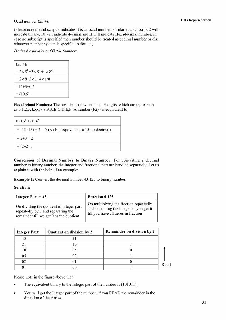
Data Representation Octal number (23.4)8 .
(Please note the subscript 8 indicates it is an octal number, similarly, a subscript 2 will indicate binary, 10 will indicate decimal and H will indicate Hexadecimal number, in case no subscript is specified then number should be treated as decimal number or else whatever number system is specified before it.)
Decimal equivalent of Octal Number:
(23.4)8
= 2×81 +3×80 +4×8-1
= 2×8+3×1+4×1/8
=16+3+0.5
= (19.5)10 Hexadecimal Numbers: The hexadecimal system has 16 digits, which are represented as 0,1,2,3,4,5,6,7,8,9,A,B,C,D,E,F. A number (F2)H is equivalent to
F×161 +2×160
= (15×16) + 2 // (As F is equivalent to 15 for decimal)
= 240 + 2
= (242)10
Conversion of Decimal Number to Binary Number: For converting a decimal number to binary number, the integer and fractional part are handled separately. Let us explain it with the help of an example: Example 1: Convert the decimal number 43.125 to binary number.
Solution:
Integer Part = 43 Fraction 0.125
On dividing the quotient of integer part repeatedly by 2 and separating the remainder till we get 0 as the quotient
On multiplying the fraction repeatedly and separating the integer as you get it till you have all zeros in fraction
Integer Part Quotient on division by 2 Remainder on division by 2
43 21 1 21 10 1 10 05 0 05 02 1 02 01 0 01 00 1 d
Please note in the figure above that:
• The equivalent binary to the Integer part of the number is (101011)2
• You will get the Integer part of the number, if you READ the remainder in the direction of the Arrow.
Rea
33

34
Introduction to Digital Circuits Fraction On Multiplication by 2 Integer part after
Multiplication 0.125 0.250 0 0.250 0.500 0 0.500 1.000 1
d
Please note in the figure above that:
• The equivalent binary to the Fractional part of the number is 001.
• You will get the fractional part of the number, if you READ the In the number in the direction of the Arrow.
Thus, the number (101011.001)2 is equivalent to .)125.43( 10
You can cross check it as follows: 1 × 25 + 0 × 24 + 1 × 23 + 0 × 22 + 1 × 21 + 1 × 20 + 0 × 2-1 + 0 × 2-2 +1= 32 + 0 + 8 + 0 + 2 + 1 + 0 + 0 +1/8
= (43.125)10
One easy direct method in Decimal to binary conversion for integer write the place values as:
26 25 24 23 22 21 20
64 32 16 8 4 2 1
Step 1: Take the integer part e.g. 43, find the next lower or equal bina number, in this example it is 32. Place 1 at 32. Step 2: Subtract the place value from the number, in this case subtrac
which is 11. Step 3: Repeat the two steps above till you get 0 at step 2. Step 4: On getting a 0 put 0 at all other place values. These steps are shown as: 32 16 8 4 2 1
32 16 8 4 2 1
1 - - - - -1 43 -32 =11
1 - 1 - - - 11- 8 = 3
1 - 1 - 1 - 3-2 = 1
1 - 1 - 1 1 1-1= 0
1 0 1 0 1 1 is the required number. You can extend this logic to fractional part also but in reverse order. Trywith several numbers. It is fast and you will soon be accustomed to it anwhole operation in single iteration.
Conversion of Binary to Octal and Hexadecimal: The rules for these are straightforward. For converting binary to octal, the binary number is
Rea
teger part of
× 2-3
part is to first
ry place value
t 32 from 43,
this method d can do the
conversions divided into

35
Data Representation groups of three, which are then combined by place value to generate equivalent octal. For example the binary number 1101011.00101 can be converted to Octal as:
1 101 011 . 001 01
001 101 011 . 001 010
1 5 3 . 1 2
(Please note the number is unchanged even though we have added 0 to complete the grouping. Also note the style of grouping before and after decimal. We count three numbers from right to left while after the decimal from left to right.)
Thus, the octal number equivalent to the binary number 1101011.00101 is (153.12)8.
Similarly by grouping four binary digits and finding equivalent hexadecimal digits for it can make the hexadecimal conversion. For example the same number will be equivalent to (6B.28)H.. 110 1011 . 0010 1
0110 1011 . 0010 1000 6 11 . 2 8
6 B . 2 8 (11in hexadecimal is B) Thus equivalent hexadecimal number is (6B.28)H
Conversely, we can conclude that a hexadecimal digit can be broken down into a string of binary having 4 places and an octal can be broken down into string of binary having 3 place values. Figure 1 gives the binary equivalents of octal and hexadecimal numbers.
Octal Number Binary coded Octal Hexadecimal Number
Binary-coded Hexadecial
0 000 0 0000 1 001 1 0001 2 010 2 0010 3 011 3 0011 4 100 4 0100 5 101 5 0101 6 110 6 0110 7 111 7 0111
8 1000
9
-Decimal- 1001
A 10 1010 B 11 1011 C 12 1100 D 13 1101 E 14 1110 F 15 1111
Figure 1: Binary equivalent of octal and hexadecimal digits

36
Introduction to Digital Circuits
Check Your Progress 1
1) Convert the following binary numbers to decimal.
i) 1100.1101
ii) 10101010
.....................................................................................................................................
.....................................................................................................................................
.....................................................................................................................................
.....................................................................................................................................
2) Convert the following decimal numbers to binary.
i) 23
ii) 49.25
iii) 892
.....................................................................................................................................
.....................................................................................................................................
.....................................................................................................................................
.....................................................................................................................................
3) Convert the numbers given in question 2 to hexadecimal from decimal or from the binary.
.....................................................................................................................................
.....................................................................................................................................
.....................................................................................................................................
.....................................................................................................................................
2.4 DECIMAL REPRESENTATION IN COMPUTERS
The binary number system is most natural for computer because of the two stable states of its components. But, unfortunately, this is not a very natural system for us as we work with decimal number system. So, how does the computer perform the arithmetic? One solution that is followed in most of the computers is to convert all input values to binary. Then the computer performs arithmetic operations and finally converts the results back to the decimal number so that we can interpret it easily. Is there any alternative to this scheme? Yes, there exists an alternative way of performing computation in decimal form but it requires that the decimal numbers should be coded suitably before performing these computations. Normally, the decimal digits are coded in 7-8 bits as alphanumeric characters but for the purpose of arithmetic calculations the decimal digits are treated as four bit binary code. As we know 2 binary bits can represent 22 = 4 different combinations, 3 bits can represent 23 = 8 combinations, and similarly, 4 bits can represent 24 = 16 combinations. To represent decimal digits into binary form we require 10 combinations, but we need to have a 4-digit code. One such simple representation may be to use first ten binary combinations to represent the ten decimal digits. These are popularly known as Binary Coded Decimals (BCD). Figure 2 shows the binary coded decimal numbers.

37
Data Representation Decimal Binary Coded Decimal
0 0000
1 0001
2 0010
3 0011
4 0100
5 0101
6 0110
7 0111
8 1000
9 1001
10 0001 0000
11 0001 0001
12 0001 0010
13 0001 0011
.. ……….
20 0010 0000
.. ………..
30 0011 0000
Figure 2: Binary Coded Decimals (BCD)
Let us represent 43.125 in BCD.
4 3 . 1 2 5
0100 0011 . 0001 0010 0101 Compare the equivalent BCD with equivalent binary value. Both are different.
2.5 ALPHANUMERIC REPRESENTATION
But what about alphabets and special characters like +, -, * etc.? How do we represent these in a computer? A set containing alphabets (in both cases), the decimal digits (10 in number) and special characters (roughly 10-15 in numbers) consist of at least 70-80 elements. ASCII
One such standard code that allows the language encoding that is popularly used is ASCII (American Standard Code for Information Interchange). This code uses 7 bits

38
Introduction to Digital Circuits
to represent 128 characters, which include 32 non-printing control characters, alphabets in lower and upper case, decimal digits, and other printable characters that are available on your keyboard. Later as there was need for additional characters to be represented such as graphics characters, additional special characters etc., ASCII was extended to 8 bits to represent 256 characters (called Extended ASCII codes). There are many variants of ASCII, they follow different code pages for language encoding, however, having the same format. You can refer to the complete set of ASCII characters on the web. The extended ASCII codes are the codes used in most of the Microcomputers.
The major strength of ASCII is that it is quite elegant in the way it represents characters. It is easy to write a code to manipulate upper/lowercase ASCII characters and check for valid data ranges because of the way of representation of characters. In the original ASCII the 8th bit (the most significant bit) was used for the purpose of error checking as a check bit. We will discuss more about the check bits later in the Unit.
EBCDIC
Extended Binary Coded Decimal Interchange Code (EBCDIC) is a character-encoding format used by IBM mainframes. It is an 8-bit code and is NOT Compatible to ASCII. It had been designed primarily for ease of use of punched cards. This was primarily used on IBM mainframes and midrange systems such as the AS/400. Another strength of EBCDIC was the availability of wider range of control characters for ASCII. The character coding in this set is based on binary coded decimal, that is, the contiguous characters in the alphanumeric range are represented in blocks of 10 starting from 0000 binary to 1001 binary. Other characters fill in the rest of the range. There are four main blocks in the EBCDIC code: 0000 0000 to 0011 1111 Used for control characters
0100 0000 to 0111 1111 Punctuation characters
1000 0000 to 1011 1111 Lowercase characters
1100 0000 to 1111 1111 Uppercase characters and numbers.
There are several different variants of EBCDIC. Most of these differ in the punctuation coding. More details on EBCDIC codes can be obtained from further reading and web pages on EBCDIC.
Comparison of ASCII and EBCDIC
EBCDIC is an easier to use code on punched cards because of BCD compatibility. However, ASCII has some of the major advantages on EBCDIC. These are: While writing a code, since EDCDIC is not contiguous on alphabets, data comparison to continuous character blocks is not easy. For example, if you want to check whether a character is an uppercase alphabet, you need to test it in range A to Z for ASCII as they are contiguous, whereas, since they are not contiguous range in EDCDIC these may have to be compared in the ranges A to I, J to R, and S to Z which are the contiguous blocks in EDCDIC.
Some of the characters such as [] \{}^~| are missing in EBCDIC. In addition, missing control characters may cause some incompatibility problems.
UNICODE
This is a newer International standard for character representation. Unicode provides a unique code for every character, irrespective of the platform, Program and Language. Unicode Standard has been adopted by the Industry. The key players that have adopted Unicode include Apple, HP, IBM, Microsoft, Oracle, SAP, Sun, Sybase, Unisys and many other companies. Unicode has been implemented in most of the

39
Data Representation latest client server software. Unicode is required by modern standards such as XML, Java, JavaScript, CORBA 3.0, etc. It is supported in many operating systems, and almost all modern web browsers. Unicode includes character set of Dev Nagari. The emergence of the Unicode Standard, and the availability of tools supporting it, is among the most significant recent global software technology trends.
One of the major advantages of Unicode in the client-server or multi-tiered applications and websites is the cost saving over the use of legacy character sets that results in targeting website and software products across multiple platforms, languages and countries without re-engineering. Thus, it helps in data transfer through many different systems without any compatibility problems. In India the suitability of Unicode to implement Indian languages is still being worked out.
Indian Standard Code for information interchange (ISCII)
The ISCII is an eight-bit code that contains the standard ASCII values till 127 from 128-225 it contains the characters required in the ten Brahmi-based Indian scripts. It is defined in IS 13194:1991 BIS standard. It supports INSCRIPT keyboard which provides a logical arrangement of vowels and consonants based on the phonetic properties and usage frequencies of the letters of Bramhi-scripts. Thus, allowing use of existing English keyboard for Indian language input. Any software that uses ISCII codes can be used in any Indian Script, enhancing its commercial viability. It also allows transliteration between different Indian scripts through change of display mode.
2.6 DATA REPRESENTATION FOR COMPUTATION
As discussed earlier, binary codes exist for any basic representation. Binary codes can be formulated for any set of discrete elements e.g. colours, the spectrum, the musical notes, chessboard positions etc. In addition these binary codes are also used to formulate instructions, which are advanced form of data representation. We will discuss about instructions in more detail in the later blocks. But the basic question which remains to be answered is: How are these codes actually used to represent data for scientific calculations?
The computer is a discrete digital device and stores information in flip-flops (see Unit 3, 4 of this Block for more details), which are two state devices, in binary form. Basic requirements of the computational data representation in binary form are:
• Representation of sign • Representation of Magnitude • If the number is fractional then binary or decimal point, and • Exponent The solution to sign representation is easy, because sign can be either positive or negative, therefore, one bit can be used to represent sign. By default it should be the left most bit (in most of the machines it is the Most Significant Bit).
Thus, a number of n bits can be represented as n+l bit number, where n+lth bit is the sign bit and rest n bits represent its magnitude (Please refer to Figure 3).
Figure 3: A (n + 1) bit number

40
Introduction to Digital Circuits
The decimal position can be represented by a position between the flip-flops (storage cells in computer). But, how can one determine this decimal position? Well to simplify the representation aspect two methods were suggested: (1) Fixed point representation where the binary decimal position is assumed either at the beginning or at the end of a number; and (2) Floating point representation where a second register is used to keep the value of exponent that determines the position of the binary or decimal point in the number.
But before discussing these two representations let us first discuss the term “complement” of a number. These complements may be used to represent negative numbers in digital computers.
Complement: There are two types of complements for a number of base (also called radix) r. These are called r’s complement and (r- 1)’s complement. For example, for decimal numbers the base is 10, therefore, complements will be 10’s complement and (10-1) = 9’s complement. For binary numbers we talk about 2’s and 1’s complements. But how to obtain complements and what do these complements means? Let us discuss these issues with the help of following example:
Example 2: Find the 9’s complement and 10’s complement for the decimal number 256.
Solution:
9’s complement: The 9’s complement is obtained by subtracting each digit of the number from 9 (the highest digit value). Let us assume that we want to represent a maximum of four decimal digit number range. 9’s complement can be used for BCD numbers.
9 -0
9 -2
9 -5
9 -6 9’s complement of 256
9 7 4 3
Similarly, for obtaining 1’s complement for a binary number we have to subtract each binary digit of the number from the digit 1.
10’s complement: Adding 1 in the 9’s complement produces the 10’s complement. 10’s complement of 0256 = 9743+1 = 9744
Please note on adding the number and its 9’s complement we get 9999 (the maximum possible number that can be represented in the four decimal digit number range) while on adding the number and its 10’s complement we get 10000 (The number just higher than the range. This number cannot be represented in four digit representation.) Example3: Find 1’s and 2’s complement of 1010 using only four-digit representation.
Solution:
1’s complement: The 1’s complement of 1010 is
1 1 1 1 -1 -0 -1 -0 0 1 0 1
The number is 1 0 1 0
The 1’s complement is 0 1 0 1
41
Data Representation Please note that wherever you have a digit 1 in number the complement contains 0 for that digit and vice versa. In other words to obtain 1’s complement of a binary number, we only have to change all the 1’s of the number to 0 and all the zeros to 1’s. This can be done by complementing each bit of the binary number.
2’s complement: Adding 1 in 1’s complement will generate the 2’s complement The number is 1 0 1 0
The 1’s complement is 0 1 0 1
For 2’s complement add 1 in 1’s complement - - - 1
Please note that 1+1 = 1 0 in binary 0 1 1 0 Most Significant bit Least significant bit
The number is 1 0 1 0
The 1’s complement is 0 1 1 0 The 2’s complement can also be obtained by not complementing the least significant zeros till the first 1 is encountered. This 1 is also not complemented. After this 1 the rest of all the bits are complemented on the left.
Therefore, 2’s complement of the following number (using this method) should be (you can check it by finding 2’s complement as we have done in the example).
The number is 0 0 1 0 0 1 0 0
The 2’s complement is 1 1 0 1 1 1 0 0
No change in these bits
The number is 1 0 0 0 0 0 0 0
The 2’s complement is 1 0 0 0 0 0 0 0
No change in number and its 2’s Complement, a special case
The number is 0 0 1 0 1 0 0 1
The 2’s complement is 1 1 0 1 0 1 1 1
No change in this bit only
2.6.1 Fixed Point Representation
The fixed-point numbers in binary uses a sign bit. A positive number has a sign bit 0, while the negative number has a sign bit 1. In the fixed-point numbers we assume that the position of the binary point is at the end, that is, after the least significant bit. It implies that all the represented numbers will be integers. A negative number can be represented in one of the following ways: • Signed magnitude representation

42
Introduction to Digital Circuits
• Signed 1’s complement representation, or • Signed 2’s complement representation. (Assumption: size of register = 8 bits including the sign bit)
Signed Magnitude Representation
Representation (8 bits) Decimal Number Sign Bit Magnitude (7 bits)
+6 0 000 0110
-6 1 000 0110
No change in the Magnitude, only sign bit changes
Signed 1’s Complement Representation
Representation (8 bits) Decimal
Number Sign Bit Magnitude/ 1’s complement for negative number (7 bits)
+6 0 000 0110
-6 1 111 1001 For negative number take 1’s complement of all the bits (including sign bit) of the positive number
Signed 2’s Complement Representation
Representation (8 bits) Decimal
Number Sign Bit Magnitude/ 1’s complement for negative number (7 bits)
+6 0 000 0110
-6 1 111 1010
For negative number take 2’s complement of all the bits (including sign bit) of the positive number
Arithmetic addition
The complexity of arithmetic addition is dependent on the representation, which has been followed. Let us discuss this with the help of following example. Example 4: Add 25 and -30 in binary using 8 bit registers, using:
• Signed magnitude representation • Signed 1’s complement • Signed 2’s complement Solution:
Signed Magnitude Representation Number
Sign Bit Magnitude +25 0 001 1001 -25 1 001 1001 +30 0 001 1110 -30 1 001 1110

43
Data Representation To do the arithmetic addition with one negative number only, we have to check the magnitude of the numbers. The number having smaller magnitude is then subtracted from the bigger number and the sign of bigger number is selected. The implementation of such a scheme in digital hardware will require a long sequence of control decisions as well as circuits that will add, compare and subtract numbers. Is there a better alternative than this scheme? Let us first try the signed 2’s complement.
Now let us perform addition using signed 2’s complement notation:
Decimal equivalent number
Signed 2’s complement representation Operation
Carry out Sign out Magnitude
Comments
+25 +30
- -
0 0
001 001
1001 1110
+55 0 0 011 0111
Simple binary addition. There is no carry out of sign bit
+25 -30
- -
0 1
001 110
1001 0010
Addition of two positive number Addition of smaller Positive and larger negative Number -05 0 1 111 1011
Perform simple binary addition. No carry in to the sign bit and no carry out of the sign bit
Positive value of result
+05 0 1 000 0101 2’s complement of above result
-25 +30
- -
1 1
110 001
0111 1110
+05 1 0 000 0101
Addition of larger Positive and smaller negative Number
Discard the carry out bit
Perform simple binary addition. No carry in to the sign bit and carry out of the sign bit
-25 -30
- 1 - 1
110 110
0111 0010
-55 1 1 110 1001
Perform simple binary addition. There is carry in
to the sign bit and carry out of the sign bit No
overflow
Addition of two negative Numbers
Discard the carry out bit
Positive value of result
+55 - 0 011 0111 2’s complemnt of above result
Signed Magnitude Representation Number
Sign Bit Magnitude
+25 0 001 1001
-25 1 110 0111
+30 0 001 1110
-30 1 110 0010
Please note how easy it is to add two numbers using signed 2’s Complement. This procedure requires only one control decision and only one circuit for adding the two numbers. But it puts on additional condition that the negative numbers should be stored in signed 2’s complement notation in the registers. This can be achieved by
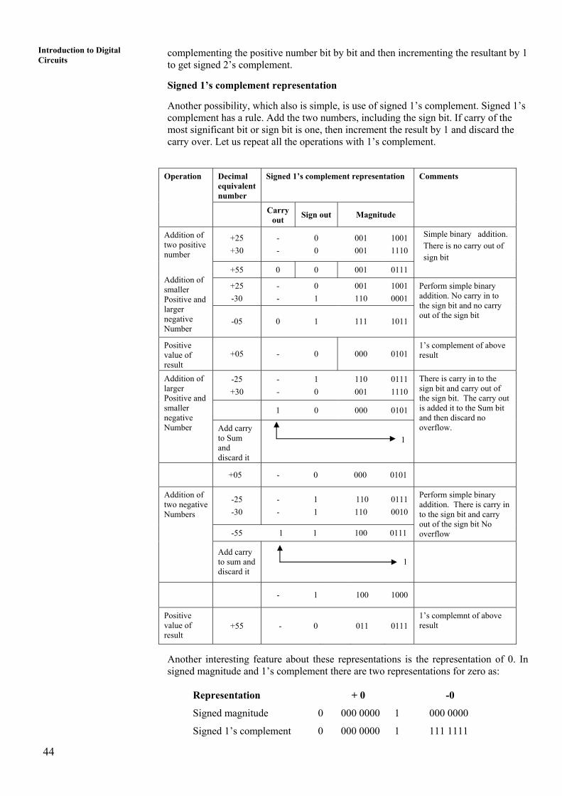
44
Introduction to Digital Circuits
complementing the positive number bit by bit and then incrementing the resultant by 1 to get signed 2’s complement.
Signed 1’s complement representation
Another possibility, which also is simple, is use of signed 1’s complement. Signed 1’s complement has a rule. Add the two numbers, including the sign bit. If carry of the most significant bit or sign bit is one, then increment the result by 1 and discard the carry over. Let us repeat all the operations with 1’s complement.
Decimal equivalent number
Signed 1’s complement representation Operation
Carry out Sign out Magnitude
Comments
+25 +30
- -
0 0
001 001
1001 1110
+55 0 0 001 0111
Simple binary addition. There is no carry out of sign bit
+25 -30
- -
0 1
001 110
1001 0001
Addition of two positive number Addition of smaller Positive and larger negative Number
-05 0 1 111 1011
Perform simple binary addition. No carry in to the sign bit and no carry out of the sign bit
Positive value of result
+05 - 0 000 0101 1’s complement of above result
-25 +30
- -
1 0
110 001
0111 1110
1 0 000 0101
Addition of larger Positive and smaller negative Number Add carry
to Sum and discard it
There is carry in to the sign bit and carry out of the sign bit. The carry out is added it to the Sum bit and then discard no overflow.
+05 - 0 000 0101
-25 -30
- 1 - 1
110 110
0111 0010
-55 1 1 100 0111
Perform simple binary addition. There is carry in to the sign bit and carry out of the sign bit No overflow
Addition of two negative Numbers
Add carry to sum and discard it
- 1 100 1000
Positive value of result
+55 - 0 011 0111 1’s complemnt of above result
1
1
Another interesting feature about these representations is the representation of 0. In signed magnitude and 1’s complement there are two representations for zero as:
Representation + 0 -0
Signed magnitude 0 000 0000 1 000 0000
Signed 1’s complement 0 000 0000 1 111 1111
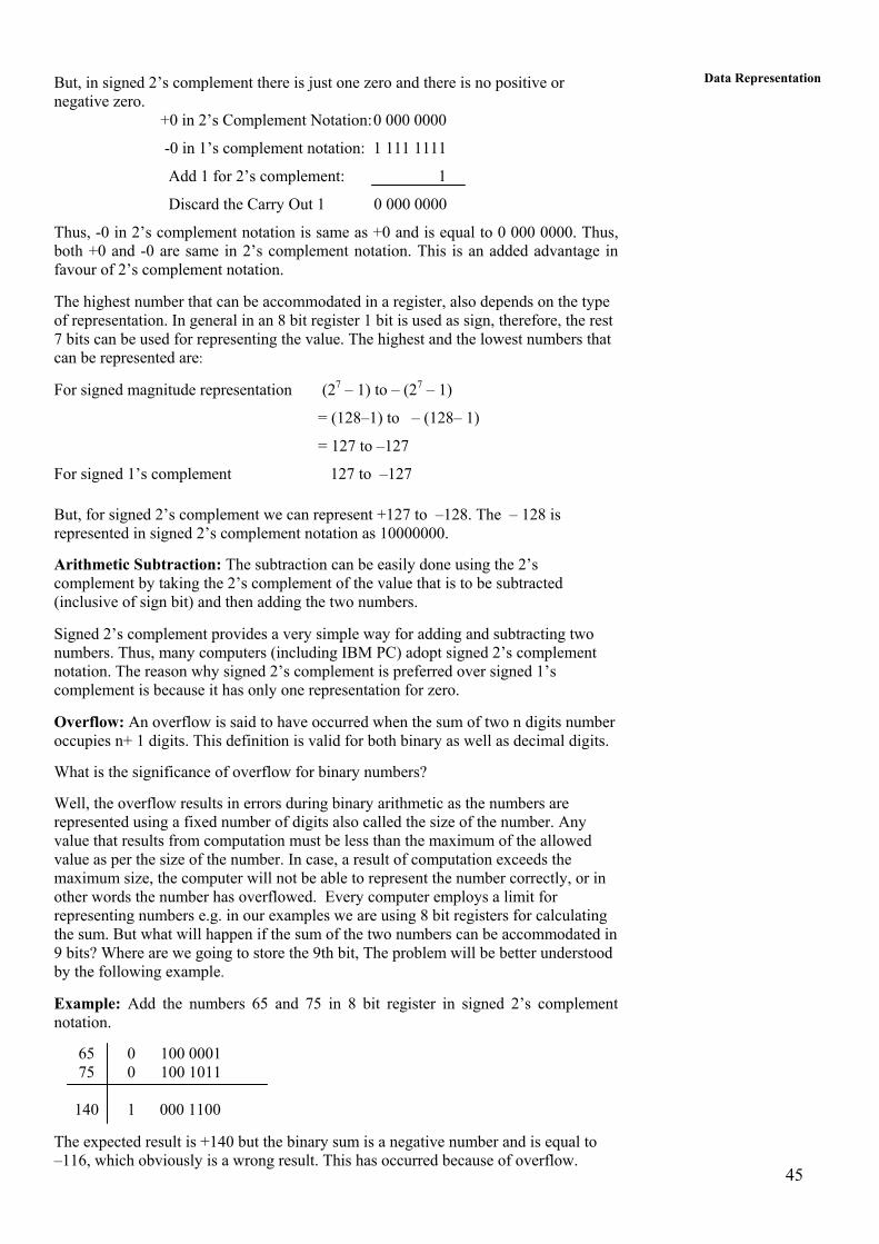
45
Data Representation But, in signed 2’s complement there is just one zero and there is no positive or negative zero. +0 in 2’s Complement Notation: 0 000 0000
-0 in 1’s complement notation: 1 111 1111
Add 1 for 2’s complement: 1
Discard the Carry Out 1 0 000 0000
Thus, -0 in 2’s complement notation is same as +0 and is equal to 0 000 0000. Thus, both +0 and -0 are same in 2’s complement notation. This is an added advantage in favour of 2’s complement notation.
The highest number that can be accommodated in a register, also depends on the type of representation. In general in an 8 bit register 1 bit is used as sign, therefore, the rest 7 bits can be used for representing the value. The highest and the lowest numbers that can be represented are:
For signed magnitude representation (27 – 1) to – (27 – 1)
= (128–1) to – (128– 1)
= 127 to –127
For signed 1’s complement 127 to –127
But, for signed 2’s complement we can represent +127 to –128. The – 128 is represented in signed 2’s complement notation as 10000000.
Arithmetic Subtraction: The subtraction can be easily done using the 2’s complement by taking the 2’s complement of the value that is to be subtracted (inclusive of sign bit) and then adding the two numbers.
Signed 2’s complement provides a very simple way for adding and subtracting two numbers. Thus, many computers (including IBM PC) adopt signed 2’s complement notation. The reason why signed 2’s complement is preferred over signed 1’s complement is because it has only one representation for zero.
Overflow: An overflow is said to have occurred when the sum of two n digits number occupies n+ 1 digits. This definition is valid for both binary as well as decimal digits.
What is the significance of overflow for binary numbers?
Well, the overflow results in errors during binary arithmetic as the numbers are represented using a fixed number of digits also called the size of the number. Any value that results from computation must be less than the maximum of the allowed value as per the size of the number. In case, a result of computation exceeds the maximum size, the computer will not be able to represent the number correctly, or in other words the number has overflowed. Every computer employs a limit for representing numbers e.g. in our examples we are using 8 bit registers for calculating the sum. But what will happen if the sum of the two numbers can be accommodated in 9 bits? Where are we going to store the 9th bit, The problem will be better understood by the following example.
Example: Add the numbers 65 and 75 in 8 bit register in signed 2’s complement notation.
65 0 100 0001 75 0 100 1011 140 1 000 1100
The expected result is +140 but the binary sum is a negative number and is equal to –116, which obviously is a wrong result. This has occurred because of overflow.

46
Introduction to Digital Circuits
How does the computer know that overflow has occurred?
If the carry into the sign bit is not equal to the carry out of the sign bit then overflow must have occurred.
Another simple test of overflow is: if the sign of both the operands is same during addition, then overflow must have occurred if the sign of resultant is different than that of sign of any operand.
For example
Decimal Carry out
Sign bit
2’s Complement Mantissa
Decimal Carry out
Sign bit
2’s Complement Mantissa
-65 -15
1 011 1111 1 111 0001
-65 -75
1 1
011 1111 111 0001
-80 1 1 011 0000 -140 1 0 111 0100
Carry into Sign bit = 1 Carry into Sign bit = 0
Carry out of sign bit = 1 Carry out of Sign bit = 1 Therefore, NO OVERFLOW Therefore, OVERFLOW
Thus, overflow has occurred, i.e. the arithmetic results so calculated have exceeded the capacity of the representation. This overflow also implies that the calculated results will be erroneous.
2.6.2 Decimal Fixed Point Representation
The purpose of this representation is to keep the number in decimal equivalent form and not binary as above. A decimal digit is represented as a combination of four bits; thus, a four digit decimal number will require 16 bits for decimal digits representation and additional 1 bit for sign. Normally to keep the convention of one decimal digit to 4 bits, the sign sometimes is also assigned a 4-bit code. This code can be the bit combination which has not been used to represent decimal digit e.g. 1100 may represent plus and 1101 can represent minus. For example, a simple decimal number – 2156 can be represented as:
1101 0010 0001 0101 0110 Sign
Although this scheme wastes considerable amount of storage space yet it does not require conversion of a decimal number to binary. Thus, it can be used at places where the amount of computer arithmetic is less than that of the amount of input/output of data e.g. calculators or business data processing situations. The arithmetic in decimal can also be performed as in binary except that instead of signed complement, signed nine’s complement is used and instead of signed 2’s complement signed 9’s complement is used. More details on decimal arithmetic are available in further readings.
Check Your Progress 2
1) Write the BCD equivalent for the three numbers given below:
i) 23
ii) 49.25
iii) 892

47
Data Representation .....................................................................................................................................
.....................................................................................................................................
.....................................................................................................................................
.....................................................................................................................................
2) Find the 1’s and 2’s complement of the following fixed-point numbers.
i) 10100010
ii) 00000000
iii) 11001100
.....................................................................................................................................
.....................................................................................................................................
.....................................................................................................................................
……………………………………………………………………………………….
3) Add the following numbers in 8-bit register using signed 2’s complement notation
i) +50 and – 5
ii) +45 and – 65
iii) +75 and +85
Also indicate the overflow if any.
.....................................................................................................................................
………………..............................................................................................................
…….. ...........................................................................................................................
…………………………………………………………………………………………
2.6.3 Floating Point Representation
Floating-point number representation consists of two parts. The first part of the number is a signed fixed-point number, which is termed as mantissa, and the second part specifies the decimal or binary point position and is termed as an Exponent. The mantissa can be an integer or a fraction. Please note that the position of decimal or binary point is assumed and it is not a physical point, therefore, wherever we are representing a point it is only the assumed position. Example 1: A decimal + 12.34 in a typical floating point notation can be represented in any of the following two forms:

48
Introduction to Digital Circuits
This number in any of the above forms (if represented in BCD) requires 17 bits for mantissa (1 for sign and 4 each decimal digit as BCD) and 9 bits for exponent (1 for sign and 4 for each decimal digit as BCD). Please note that the exponent indicates the correct decimal location. In the first case where exponent is +2, indicates that actual position of the decimal point is two places to the right of the assumed position, while exponent– 2 indicates that the assumed position of the point is two places towards the left of assumed position. The assumption of the position of point is normally the same in a computer resulting in a consistent computational environment. Floating-point numbers are often represented in normalised forms. A floating point number whose mantissa does not contain zero as the most significant digit of the number is considered to be in normalised form. For example, a BCD mantissa + 370 which is 0 0011 0111 0000 is in normalised form because these leading zero’s are not part of a zero digit. On the other hand a binary number 0 01100 is not in a normalised form. The normalised form of this number is:
0 1100 0100 Sign Normalised Mantissa Exponent (assuming fractional Mantissa
A floating binary number +1010.001 in a 16-bit register can be represented in normalised form (assuming 10 bits for mantissa and 6 bits for exponent).
Exponent Mantissa (Integer)
0 00100 1010001000
Sign bit
A zero cannot be normalised as all the digits in mantissa in this case have to be zero.
Arithmetic operations involved with floating point numbers are more complex in nature, take longer time for execution and require complex hardware. Yet the floating-point representation is a must as it is useful in scientific calculations. Real numbers are normally represented as floating point numbers.
The following figure shows a format of a 32-bit floating-point number.
Sign Biased Exponent = 8 bits Significand = 23 bits 90 1
Figure 4: Floating Point Number Representation
The characteristics of a typical floating-point representation of 32 bits in the above figure are:
• Left-most bit is the sign bit of the number; • Mantissa or signific and should be in normalised form; • The base of the number is 2, and • A value of 128 is added to the exponent. (Why?) This is called a bias. A normal exponent of 8 bits normally can represent exponent values as 0 to 255. However, as we are adding 128 for getting the biased exponent from the actual exponent, the actual exponent values represented in the range will be – 128 to 127. Now, let us define the range that a normalised mantissa can represent. Let us assumthat our present representations has the normalised mantissa, thus, the left most bit
31
8e

49
Data Representation cannot be zero, therefore, it has to be 1. Thus, it is not necessary to store this first bit and it is being assumed implicitly for the number. Therefore, a 23-bit mantissa can represent 23 + 1 = 24 bit mantissa in our representation.
Thus, the smallest mantissa value may be:
The implicit first bit as 1 followed by 23 zero’s, that is, 0.1000 0000 0000 0000 0000 0000 Decimal equivalent = 1 × 2-1 = 0.5 The Maximum value of the mantissa: The implicit first bit 1 followed by 23 one’s, that is, 0.1111 1111 1111 1111 1111 1111
Decimal equivalent: For finding binary equivalent let us add 2-24 to above mantissa as follows:
Binary: 0.1111 1111 1111 1111 1111 1111
+0.0000 0000 0000 0000 0000 0001 = 2-24
1.0000 0000 0000 0000 0000 0000 = 1 = (1 – 2-24)
Therefore, in normalised mantissa and biased exponent form, the floating-point number format as per the above figure, can represent binary floating-point numbers in the range:
Smallest Negative number Maximum mantissa and maximum exponent = – (1 –2-24) × 2127
Largest negative number Minimum mantissa and Minimum exponent = -0.5 × 2-128
Smallest positive number = 0.5 × 2-128
Largest positive number = (1 –2-24) × 2127
Figure 5: Binary floating-point number range for given 32 bit format

50
Introduction to Digital Circuits
In floating point numbers, the basic trade-off is between the range of the numbers and accuracy, also called the precision of numbers. If we increase the exponent bits in 32-bit format, the range can be increased, however, the accuracy of numbers will go down, as size of mantissa will become smaller. Let us take an example, which will clarify the term precision. Suppose we have one bit binary mantissa then we can represent only 0.10 and 0.11 in the normalised form as given in above example (having an implicit 1). The values such as 0.101, 0.1011 and so on cannot be represented as complete numbers. Either they have to be approximated or truncated and will be represented as either 0.10 or 0.11. Thus, it will create a truncation or round off error. The higher the number of bits in mantissa better will be the precision.
In floating point numbers, for increasing both precision and range more number of bits are needed. This can be achieved by using double precision numbers. A double precision format is normally of 64 bits.
Institute of Electrical and Electronics Engineers (IEEE) is a society, which has created lot of standards regarding various aspects of computer, has created IEEE standard 754 for floating-point representation and arithmetic. The basic objective of developing this standard was to facilitate the portability of programs from one to another computer. This standard has resulted in development of standard numerical capabilities in various microprocessors. This representation is shown in figure 6.
0 1 8 9 31
S Biased exponent (E) Significand (N)
Single Precision = 32 bits
0 1 11 12 63
S
Biased exponent (E)
Significand (N)
Double Precision = 64 bits
Figure 6: IEEE Standard 754 format
Figure 7 gives the floating-point numbers specified by the IEEE Standard 754.
Single Precision Numbers (32 bits)
Exponent (E) Significand (N) Value / Comments 255 Not equal to 0 Do represent a number 255 0 - or +∞ depending on sign bit 0<E<255 Any ± (1.N) 2E-127
For example, if S is zero that is positive number. N=101 (rest 20 zeros) and E=207 Then the number is = +(1.101) 2207-127 = + 1.101×280
0 Not equal to 0 ± (0.N) 2-126 0 0 ± 0 depending on the sign bit. Double precision Numbers (64 bits)
Exponent (E) Significand (N) Value / Comments 2047 Not equal to 0 Do not represent a number
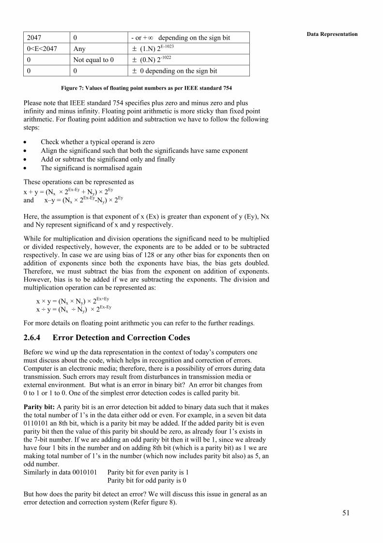
51
Data Representation 2047 0 - or + depending on the sign bit ∞
0<E<2047 Any ± (1.N) 2E-1023 0 Not equal to 0 ± (0.N) 2-1022 0 0 ± 0 depending on the sign bit
Figure 7: Values of floating point numbers as per IEEE standard 754
Please note that IEEE standard 754 specifies plus zero and minus zero and plus infinity and minus infinity. Floating point arithmetic is more sticky than fixed point arithmetic. For floating point addition and subtraction we have to follow the following steps:
• Check whether a typical operand is zero • Align the significand such that both the significands have same exponent • Add or subtract the significand only and finally • The significand is normalised again
These operations can be represented as x + y = (Nx × 2Ex-Ey + Ny) × 2Ey and x–y = (Nx × 2Ex-Ey-Ny) × 2Ey
Here, the assumption is that exponent of x (Ex) is greater than exponent of y (Ey), Nx and Ny represent significand of x and y respectively.
While for multiplication and division operations the significand need to be multiplied or divided respectively, however, the exponents are to be added or to be subtracted respectively. In case we are using bias of 128 or any other bias for exponents then on addition of exponents since both the exponents have bias, the bias gets doubled. Therefore, we must subtract the bias from the exponent on addition of exponents. However, bias is to be added if we are subtracting the exponents. The division and multiplication operation can be represented as:
x × y = (Nx × Ny) × 2Ex+Ey x ÷ y = (Nx ÷ Ny) × 2Ex-Ey
For more details on floating point arithmetic you can refer to the further readings.
2.6.4 Error Detection and Correction Codes
Before we wind up the data representation in the context of today’s computers one must discuss about the code, which helps in recognition and correction of errors. Computer is an electronic media; therefore, there is a possibility of errors during data transmission. Such errors may result from disturbances in transmission media or external environment. But what is an error in binary bit? An error bit changes from 0 to 1 or 1 to 0. One of the simplest error detection codes is called parity bit.
Parity bit: A parity bit is an error detection bit added to binary data such that it makes the total number of 1’s in the data either odd or even. For example, in a seven bit data 0110101 an 8th bit, which is a parity bit may be added. If the added parity bit is even parity bit then the value of this parity bit should be zero, as already four 1’s exists in the 7-bit number. If we are adding an odd parity bit then it will be 1, since we already have four 1 bits in the number and on adding 8th bit (which is a parity bit) as 1 we are making total number of 1’s in the number (which now includes parity bit also) as 5, an odd number. Similarly in data 0010101 Parity bit for even parity is 1 Parity bit for odd parity is 0
But how does the parity bit detect an error? We will discuss this issue in general as an error detection and correction system (Refer figure 8).

52
Introduction to Digital Circuits
The error detection mechanism can be defined as follows:
Figure 8: Error detection and correction
The Objective : Data should be transmitted between a source data pair reliably, indicating error, or even correcting it, if possible.
The Process:
• An error detection function is applied on the data available at the source end an error detection code is generated.
• The data and error detection or correction code are stored together at source. • On receiving the data transmission request, the stored data along with stored
error detection or correction code are transmitted to the unit requesting data (Destination).
• On receiving the data and error detection/correction code from source, the destination once again applies same error detection/correction function as has been applied at source on the data received (but not on error detection/ correction code received from source) and generates destination error detection/correction code.
• Source and destination error codes are compared to flag or correct an error as the case may be.
The parity bit is only an error detection code. The concept of error detection and correction code has been developed using more than one parity bits. One such code is Hamming error correcting code.
Hamming Error-Correcting Code: Richard Hamming at Bell Laboratories devised this code. We will just introduce this code with the help of an example for 4 bit data.
Let us assume a four bit number b4, b3, b2, b1. In order to build a simple error detection code that detects error in one bit only, we may just add an odd parity bit. However, if we want to find which bit is in error then we may have to use parity bits for various combinations of these 4 bits such that a bit error can be identified uniquely. For example, we may create four parity sets as
Source Parity Destination Parity

53
Data Representation b1, b2, b3 P1 D1
b2, b3, b4 P2 D2
b3, b4, b1 P3 D3
b1, b2, b3, b4 P4 D4
Now, a very interesting phenomena can be noticed in the above parity pairs. Suppose data bit b1 is in error on transmission then, it will cause change in destination parity D1, D3, D4.
ERROR IN Cause change in Destination Parity (one bit only)
b1 D1, D3, D4
b2 D1, D2, D4
b3 D1, D2,D3, D4
b4 D2, D3, D4
Figure 9 : The error detection parity code mismatch
Thus, by simply comparing parity bits of source and destination we can identify that which of the four bits is in error. This bit then can be complemented to remove error. Please note that, even the source parity bit can be in error on transmission, however, under the assumption that only one bit (irrespective of data or parity) is in error, it will be detected as only one destination parity will differ. What should be the length of the error detection code that detects error in one bit? Before answering this question we have to look into the comparison logic of error detection. The error detection is done by comparing the two ‘i’ bit error detection and correction codes fed to the comparison logic bit by bit (refer to figure 8). Let us have comparison logic, which produces a zero if the compared bits are same or else it produces a one.
Therefore, if similar Position bits are same then we get zero at that bit Position, but if they are different, that is, this bit position may point to some error, then this Particular bit position will be marked as one. This way a matching word is constructed. This matching word is ‘i’ bit long, therefore, can represent 2i values or combinations.
For example, a 4-bit matching word can represent 24=16 values, which range from 0 to 15 as:
0000, 0001, 0010, 0011, 0100, 0101, 0110, 0111
1000, 1001, 1010, 1011, 1100, 1101, 1110, 1111 The value 0000 or 0 represent no error while the other values i.e. 2i-1 (for 4 bits 24– 1=15, that is from 1 to 15) represent an error condition. Each of these 2i – 1(or 15 for 4 bits) values can be used to represent an error of a particular bit. Since, the error can occur during the transmission of ‘N’ bit data plus ‘i’ bit error correction code, therefore, we need to have at least ‘N+i’ error values to represent them. Therefore, the number of error correction bits should be found from the following equation: 2i – 1 >= N+i
If we are assuming 8-bit word then we need to have
2i – 1 >= 8+i
Say at i=3 LHS = 23 –1 = 7; RHS = 8+3 = 11

54
Introduction to Digital Circuits i=4 2i-1 = 24 – 1 = 15; RHS = 8+4 = 12
Therefore, for an eight-bit word we need to have at least four-bit error correction code for detecting and correcting errors in a single bit during transmission.
Similarly for 16 bit word we need to have i = 5
25 –1 = 31 and 16+i = 16+5 = 21
For 16-bit word we need to have five error correcting bits.
Let us explain this with the help of an example:
Let us assume 4 bit data as 1010
The logic is shown in the following table:
Source:
Source Data Odd parity bits at source
b4 b3
b2
b1
P1 (b1, b2, b3)
P2 (b2, b3, b4)
P3 (b3, b4, b1)
P4 (b1, b2, b3,b4 )
1 0 1 0 0 1 0 1
This whole information, that is (data and P1 to P4), is transmitted.
Assuming one bit error in data.
Case 1: Data received as 1011 (Error in b1)
b4 b3
b2
b1
D1 (b1, b2, b3)
D2 (b2, b3, b4)
D3 (b3, b4, b1)
D4 (b1, b2, b3,b4 )
1 0 1 0 0 1 0 1
Thus, P1 – D1, P3 – D3, P4 –D4 pair differ, thus, as per Figure 9, b1 is in error, so correct it by completing b1 to get correct data 1010.
Case 2: Data Received as 1000 (Error in b2)
b4 b3
b2
b1
D1 (b1, b2, b3)
D2 (b2, b3, b4)
D3 (b3, b4, b1)
D4 (b1, b2, b3,b4 )
1 0 0 0 0 1 0 0
Thus, P1 – D1, P2 – D2, P4 – D4 pair differ, thus, as per figure 9,bit b2 is in error. So correct it by complementing it to get correct data 1010.
Case 3:
Now let us take a case when data received is correct but on receipt one of the parity bit, let us say P4 become 0. Please note in this case since data is 1010 the destination parity bits will be D1=0, D2=1, D3=0, D4=1. Thus, P1– D1, P2 – D2, P3 – D3, will be same but P4 –D4 differs. This does not belong to any of the combinations in Figure 9. Thus we conclude that P4 received is wrong.
Please not that all these above cases will fail in case error is in more than one bits. Let us see by extending the above example.

55
Data Representation Normally, Single Error Correction (SEC) code is used in semiconductor memories for correction of single bit errors, however, it is supplemented with an added feature for detection of errors in two bits. This is called a SEC-DED (Single Error Correction- Double Error Detecting) code. This code requires an additional check bit in comparison to SEC code. We will only illustrate the working principle of SEC-DED code with the help of an example for a 4-bit data word. Basically, the SEC-DED code guards against the errors of two bits in SEC codes.
Case: 4
Let us assume now that two bit errors occur in data. Data received:
b4 b3 b2 b1 1 1 0 0
b4 b3
b2
b1
D1 (b1, b2, b3)
D2 (b2, b3, b4)
D3 (b3, b4, b1)
D4 (b1, b2, b3,b4 )
1 0 0 0 0 1 0 0
Thus, on -matching we find P3-D3 pair does not match. However, this information is wrong. Such problems can be identified by adding one more bit to this Single Error Detection Code. This is called Double Error Detection bit (P5, D5).
So our data now is
b4 b3 b2 b1 P1 P2 P3 P4 P5
1 0 1 0 0 1 0 1 1
(Overall parity of whole data)
Data receiving end.
b4 b3 b2 b1 D1 D2 D3 D4 D5
1 1 0 0 0 1 1 1 0
D5–P5 mismatch indicates that there is double bit error, so do not try to correct error, instead asks the sender to send the data again. Thus, the name single error correction, but double error detection, as this code corrects single bit errors but only detects error in two bit.
Check Your Progress 3
1) Represent the following numbers in IEEE-754 floating point single precision number format:
i) 1010. 0001 ii) –0.0000111
2) Find the even and odd parity bits for the following 7-bit data:
i) 0101010 ii) 0000000 iii) 1111111 iv) 1000100
.....................................................................................................................................
.....................................................................................................................................
3) Find the length of SEC code and SEC-DED code for a 16-bit word data transfer.

56
Introduction to Digital Circuits
.....................................................................................................................................
.....................................................................................................................................
.....................................................................................................................................
2.7 SUMMARY
This unit provides an in-depth coverage of the data representation in a computer system. We have also covered aspects relating to error detection mechanism. The unit covers number system, conversion of number system, conversion of numbers to a different number system. It introduces the concept of computer arithmetic using 2’s complement notation and provides introduction to information representation codes like ASCII, EBCDIC, etc. The concept of floating point numbers has also been covered with the help of a design example and IEEE-754 standard. Finally error detection and correction mechanism is detailed along with an example of SEC & SEC-DED code.
The information given on various topics such as data representation, error detection codes etc. although exhaustive yet can be supplemented with additional reading. In fact, a course in an area of computer must be supplemented by further reading to keep your knowledge up to date, as the computer world is changing with by leaps and bounds. In addition to further reading the student is advised to study several Indian Journals on computers to enhance his knowledge.
2.8 SOLUTIONS/ANSWERS
Check Your Progress 1
1.
(i) 23 22 21 20 2-1 2-2 2-3 2-4 1 1 0 0 1 1 0 1 thus; Integer = (1×23+1×22+0×21+0×20) = (23+22) = (8+4) = 12 Fraction = (1×2-1+1×2-2+0×2-3+1×2-4) = 2-1+2-2+2-4 = 0.5+0.125 + 0.0625 =0.6875
ii) 10101010
27 2
6 2
5 2
4 2
3 2
2 2
1 2
0
1 0 1 0 1 0 1 0
128 64 32 16 8 4 2 1
=1 0 1 0 1 0 1 0
The decimal equivalent is
= 1× 128 + 0×64 + 1×32 + 0×16 + 1×8 + 0×4 + 1×2 + 0×1
= 128 + 32 + 8 + 2 = 170
2.
i) 16 8 4 2 1
1 0 1 1 1
ii) Integer is 49.

57
Data Representation 32 16 8 4 2 1
1 1 0 0 0 1
Fraction is 0.25
1/2 1/4 1/8 1/16
0 1 0 0
The decimal number 49.25 is 110001.010
iii)
512 256 128 64 32 16 8 4 2 1
1 1 0 1 1 1 1 1 0 0
The decimal number 892 in binary is 1101111100
3)
i) Decimal to Hexadecimal
16) 23 (1 -16 7
Hexadecimal is 17 Binary to Hexadecimal (hex)
= 1 0111 (from answer of 2 (i)
0001 0111 1 7
ii) 49.25 or 110001.010
Decimal to hex
Integer part = 49
16 ) 49 ( 3 -48
1
Integer part = 31
Fraction part = .25 ×16
= 4.000 So fraction part = 4
Hex number is 31.4
Binary to hex 11 0001 . 010 = 0011 0001 . 0100 = 3 1 . 4 = 31.4
iii) 892 or 1101111100
0011 0111 1100 = 3 7 C = 37C
Number Quotient on division by 16
Remainder

58
Introduction to Digital Circuits
892
55
3
55
3
0
12=C
7
3
So the hex number is : 37C
Check Your Progress 2
1.
i) 23 in BCD is 0010 0011
ii) 49.25 in BCD is 0100 1001.0010 0101
iii) 892 in BCD is 1000 1001 0010
2. 1’s complement is obtained by complementing each bit while 2’s complement is obtained by leaving the number unchanged till first 1starting from least significant bit after that complement each bit.
(i) (ii) (iii)
Number 10100010 00000000 11001100
1’s complement 01011101 11111111 00110011
2’s complement 01011110 00000000 00110100
3. We are using signed 2’s complement notation
(i) +50 is 0 0110010 +5 is 0 0000101 therefore –5 is 1 1111011
Add+50 = 0 0110010
– 5 1 1111011
1 0 0101101 ^
carry out (discard the carry)
Carry in to sign bit = 1
Carry out of sign bit = 1 Therefore, no overflow
The solution is 0010 1101= +45
ii) +45 is 0 0101101 +65 is 0 1000001 Therefore, -65 is 1 0111111 +45 0 0101101 – 65 1 0111111 1 1101100
No carry into sign bit, no carry out of sign bit. Therefore, no overflow.
+20 is 0 0010100
Therefore, -20 is 1 1101100
which is the given sum

59
Data Representation (iii) +75 is 0 1001011 +85 is 0 1010101
1 0100000 Carry into sign bit = 1 Carry out of sign bit = 0 Overflow.
Check Your Progress 3
1.
i) 1010.0001 = 1.0100001 ×23 So, the single precision number is : Significand = 010 0001 000 0000 0000 0000 Exponent = 3+127 = 130 = 10000010 Sign=0 So the number is = 0 1000 0010 010 0001 0000 0000 0000 0000 ii) -0.0000111 -1.11×2-5 Significand = 110 0000 0000 0000 0000 0000 Exponent = 127-5 = 122 = 0111 1010 Sign = – 1 ≡So the number is 1 0111 1010 110 0000 0000 0000 0000 0000 2. Data Even parity bit Odd parity bit 0101010 1 0 0000000 0 1 1111111 1 0 1000100 0 1
3. The equation for SEC code is 2i -1 > =N+i i — Number of bits in SEC code N — Number of bits in data word
In, this case N = 16 i = ?
so the equation is
2i – 1 > =16 + i
at i = 4 24 -1 > =16+4 15 > = 20 Not true.
at i = 5 25 -1 > =16+5 31> = 21 True the condition is satisfied.
Although, this condition will be true for i > 5 also but we want to use only minimum essential correction bits which are 5.
For SEC-DED code we require an additional bit as overall parity. Therefore, the SEC-DED code will be of 6 bits.

60
Introduction to Digital Circuits UNIT 3 PRINCIPLES OF LOGIC CIRCUITS I
Structure Page Nos.
3.0 Introduction 60 3.1 Objectives 60 3.2 Logic Gates 60 3.3 Logic Circuits 62 3.4 Combinational Circuits 63 3.4.1 Canonical and Standard Forms 3.4.2 Minimization of Gates 3.5 Design of Combinational Circuits 72 3.6 Examples of Logic Combinational Circuits 73 3.6.1 Adders 3.6.2 Decoders 3.6.3 Multiplexer 3.6.4 Encoder 3.6.5 Programmable Logic Array 3.6.6 Read Only Memory ROM 3.7 Summary 82 3.8 Solutions/ Answers 82
3.0 INTRODUCTION
In the previous units, we have discussed the basic configuration of computer system von Neumann architecture, data representation and simple instruction execution paradigm. But ‘How does a computer actually perform computations?’. Now, we will attempt to find answer of this basic query. In this unit, you will be exposed to some of the basic components that form the most essential parts of a computer. You will come across terms like logic gates, binary adders, logic circuits and combinational circuits etc. These circuits are the backbone of any computer system and knowing them is quite essential. The characteristics of integrated digital circuits are also discussed in this unit.
3.1 OBJECTIVES
After going through this unit you will be able to:
• define logic gates; • describe the significance of Boolean algebra in digital circuit design; • describe the necessity of minimizing the number of gates in design; • describe how basic mathematical operations, viz. addition and subtraction, are performed by computer; and • define and describe some of the useful circuits of a computer system such as multiplexer, decoders, ROM etc.
3.2 LOGIC GATES A logic gate is an electronic circuit which produces a typical output signal depending on its input signal. The output signal of a gate is a simple Boolean operation of its input signal. Gates are the basic logic elements that produce signals of binary 1 or 0.
We can represent any Boolean function in the form of gates.

61
Principles of Logic Circuits I
In general we can represent each gate through a distinct graphic symbol and its operation can be given by means of algebraic expression. To represent the input-output relationship of binary variables in each gate, truth tables are used. The notations and truth -tables for different logic gates are given in Figure 3.1.
Figure 3.1: Logic Gates
The truth table of NAND and NOR can be made from NOT (A AND B) and NOT (A OR B) respectively. Exclusive OR (XOR) is a special gate whose output is one only if the two inputs are not equal. The inverse of exclusive OR, called as XNOR gate, can be a comparator which will produce a 1 output if two inputs are equal.
The digital circuits use only one or two types of gates for simplicity in fabrication purposes. Therefore, one must think in terms of functionally complete set of gates. What does functionally complete set imply? A set of gates by which any Boolean function can be implemented is called a functionally complete set. The functionally complete sets are: [AND, NOT], [NOR], [NAND], [OR, NOT].

62
Introduction to Digital Circuits 3.3 LOGIC CIRCUITS
A Boolean function can be implemented into a logic circuit using the basic gates:- AND , OR & NOT. Consider, for example, the Boolean function: - F (A,B,C) = A B + C
The relationship between this function and its binary variables A, B, C can be represented in a truth table as shown in figure 3.2(a) and figure 3.2(b) shows the corresponding logic circuit.
Inputs Output
A B C F
0 0 0 0
0 0 1 1 0 1 0 1 0 1 1 1 1 0 0 0 1 0 1 1 1 1 0 0 1 1 1 1
(a) Truth Table (b) Logic Circuit
Figure 3.2 : Truth table & logic diagram for F = A B + C
Thus, in a logic circuit, the variables coming on the left hand side of boolean expression are inputs to circuit and the variable function coming on the right hand side of expression is taken as output.
Here, there is one important point to note i.e. there is only one way to represent the boolean expression in a truth table but can be expressed in variety of logic circuits. How? [try to find the answer]
Check Your Progress 1
1) What are the logic gates and which gates are called as Universal gates. .....................................................................................................................................
.....................................................................................................................................
2) Simplify the Boolean function: F =
++
+ BABA
……………………………………………………………………………………….
……………………………………………………………………………………….
……………………………………………………………………………………….
3) Draw the logic diagram of the above function.
.....................................................................................................................................
.....................................................................................................................................
.....................................................................................................................................
………………………………………………………………………………………..

63
Principles of Logic Circuits I
4) Draw the logic diagram of the simplified function.
.....................................................................................................................................
.....................................................................................................................................
5) Show implementation of AND, NOT and OR Operations using NAND gates.
……………………………………………………………………………………….
……………………………………………………………………………………….
……………………………………………………………………………………….
3.4 COMBINATIONAL CIRCUIT
Combinational circuits are interconnected circuits of gates according to certain rules to produce an output depending on its input value. A well-formed combinational circuit should not have feedback loops. A combinational circuit can be represented as a network of gates and, therefore, can be expressed by a truth table or a Boolean expression. The output of the combinational circuit is related to its input by a combinational function, which is independent of time. Therefore, for an ideal combinational circuit the output should change instantaneously according to changes in input. But in actual case there is a slight delay. The delay is normally proportional to depth or number of levels i.e. the maximum numbers of gates on any path from input to output. For example, the depth of the combinational circuit in figure 3.3 is 2.
Figure 3.3 : A two level AND-OR combinational circuit
The basic design issue related to combinational circuits is: the Minimization of number of gates. The normal circuit constraints for combinational circuit design are :
• The depth of the circuit should not exceed a specific level, • Number of input lines to a gate (fan in) and to how many gates its output can be fed (fan out) are constraint by the circuit power constraints.
3.4.1 Canonical and Standard Forms
An algebric expression can exist in two forms :
i) Sum of Products (SOP) e.g. (A . B ) + ( A . B ) ii) Product of Sums (POS) e.g. ( A + B ) . (A + B)
If a product term of SOP expression contains every variable of that function either in true or complement form then it is defined as a Minterm or Standard Product. This minterm will be true only for one combination of input values of the variables. For example, in the SOP expression
F (A, B, C) = (A. B.C) + ( A . B . C) + (A . B) We have three product terms namely A.B.C, . A . B .C and A.B. But only first two of them qualifies to be a minterm, as the third one does not contain variable C or its

64
Introduction to Digital Circuits
complement. In addition, the term A.B.C will be one only if A = 1, B = 1and C = 1, for any other combination of values of A, B, C the minterm A.B.C will have 0 value. Similarly, the minterm. A B . C will have value 1 only if A = 1, B = 1 and C = 1 (It implies A=0, B=0 and C=1) for any other combination of values the minterm will have a zero value. Similar type of term used in POS form is called Maxterm or Standard Sums . Maxterm is a term of POS expression, which contains all the variables of the function in true or complemented form. For example, F (A, B, C) = (A + B + C). ( A + B + C) has two maxterms. A maxterm has a value 0, for only one combination of input values.
The maxterm A + B+C will has 0 value only for A = 0, B = 0 and C = 0 for all other combination of values of A, B, C it will have a value 1.
Figure 3.4 indicates the 2n different minterms and maxterms where n is number of variables.
Variable’s Value Minterm Maxterm a b c Term Representation Term Representation 0 0 0 a b c m0 a + b+ c M0
0 0 1 a b c m1 a +b + c M1 0 1 0 a b c m2 a + b + c M2 0 1 1 a b c m3 a + b + c M3
1 0 0 a b c m4 a + b+ c M4
1 0 1 a b c m5 a + b+ c M5 1 1 0 a b c m6 a + b + c M6 1 1 1 a b c m7 a + b + c M7
Figure 3.4: Maxterms and Minterms for 3 variables
We can represent any Boolean function alegebrically directly in minterm and maxterm form from the truth table. For minterms, consider each combination of variables that produces a 1 output in function and then taking OR of all those terms. For example, the function F in figure 3.5 is represented in minterm form by ORing the terms where the output F is 1 i.e. a b c , a b c a b c, a b c & a b c .
a b c F 0 0 0 0 m0 0 0 1 1 m1 0 1 0 1 m2 0 1 1 1 m3 1 0 0 0 m4 1 0 1 0 m5 1 1 0 1 m6 1 1 1 1 m7
Figure 3.5: Function of three variables
Thus, F (a,b,c) = a b c + a b c + a b c+ a b c + a b c
= m1 + m2+ m3 + m6 + m7
= ∑ (1,2,3,6,7)

65
Principles of Logic Circuits I
The complement of function F can be obtained by ORing of the minterms corresponding to the combinations that produce a 0 output in function. Thus,
F (a, b, c) = a b c + a b c + a b c
If we take the complement of F , we get the function F in maxterm form.
F (a, b, c) = ( F ) = ( a b c + a b c + a b c) = ( a b c ) . (a b c ) . (a b c) = (a + b + c) ( a + b + c) ( a + b + c ) [De Morgan’s law] = M0 . M4 . M5 = Π (0, 4, 5) The product symbol stands for ANDing the maxterms. ΠHere, you will appreciate the fact that the terms which were missing in minterm form are present in maxterm form. Thus if any form is known then the other form can be directly formed.
The Boolean function expressed as a sum of minterms or product of maxterms has the property that each and every literal of the function should be present in each and every term in either normal or complemented form.
3.4.2 Minimization of Gates
The simplification of Boolean expression is very useful for combinational circuit design. The following three methods are used for this:
• Algebraic Simplification • Karnaugh Maps • Quine McCluskey Method Algebraic Simplification
We have already discussed algebraic simplification of logic circuit. An algebraic expression can exist in POS or SOP forms. Let us examine the following example to understand how it helps in implementing any logic circuit. Example : Consider the function F (a,b,c) = a b c + a b c + a b . The logic circuit
implementation of this function is shown in fig 3.6(a).
(a) F = bacbacb ++a

66
Introduction to Digital Circuits
(b) F = bacbacb ++a
Figure 3.6 : Two logic diagrams for same boolean expression
The expression F can be simplified using boolean algebra. F(a,b,c) = a b c + a b c + a b = a b ( c + c) + a b [ as c + c = 1] = a b + a b = a⊕b
The logic diagram of the simplified expression is drawn in fig 3.6 (b) using NOT, OR and AND gates (the same operation can be performed by using a single XOR gate). Thus the number of gates are reduced to 5 gates (2 inverters, 2 AND gates & 1 OR) instead of 7 gates. (3 inverters, 3 AND & 1 OR gate).
The algebraic function can appear in many different forms although a process of simplification exists yet it is cumbersome because of absence of routes which tell what rule to apply next. The Karnaugh map is a simple direct approach of simplification of logic expressions.
Karnaugh Maps
Karnaugh maps are a convenient way of representing and simplifying Boolean function of 2 to 6 variables. The stepwise procedure for Karnaugh map is.
Step 1: Create a simple map depending on the number of variables in the function. Figure 3.7(a) shows the map of two, three and four variables. A map of 2 variables contains 4 value position or elements, while for 3 variables it has 23 = 8 elements. Similarly for 4 variables it is 24 =16 elements and so on. Special care is taken to represent variables in the map. The value of only one variable changes in two adjacent columns or rows. The advantage of having change in one variable is that two adjacent cloumns or rows represent a true or complement form of a single variable.
For example, in figure 3.7(a) the columns which have positive A are adjacent and so are the column for A . Please note the adjacency of the corners. The right most column can be considered to be adjacent to the first column since they differ only by one variable and are adjacent. Similarly the top most and bottom most rows are adjacent.

67
Principles of Logic Circuits I
(a) Maps for 2, 3 and 4 variables
(b) Possible adjacencies
Figure 3.7: Maps and their adjacencies
Please note:
1) Decimal equivalents of column are given for help in understanding where the position of the respective set lies. It is not the value filled in the square. A square can contain one or nothing.
2) The 00, 01, 11 etc written on the top implies the value of the respective variables.
3) Wherever the value of a variable is 0 it is said to represent its compliment form. 4) The value of only one variable changes when we move from one row to the next
row or one column to the next column.
Step 2: The next step in Karnaugh map is to map the truth table into the map. The mapping is done by putting a 1 in the respective square belonging to the 1 value in the truth table. This mapped map is used to arrive at simplified Boolean expression which then can be used for drawing up the optimal logical circuit. Step 2 will be more clear in the example.
Step 3: Now, create simple algebraic expression from the K-Map. These expressions are created by using adjacency if we have two adjacent 1’s then the expression for those can be simplified together since they differ only in 1 variable. Similarly, we search for the adjacent pairs of 4, 8 and so on. A 1 can appear in more than one adjacent pairs. We should search for octets first then quadrets and then for doublets. The following example will clarify the step 3.

68
Introduction to Digital Circuits
Example: Now, let us see how to use K map simplification for finding the Boolean function for the cases whose truth table is given in figure 3.8(a) and 3.8(B) shows the K-Map for this.
Decimal A B C D Output F
0 0 0 0 0 1
1 0 0 0 1 1
2 0 0 1 0 1
3 0 0 1 1 0
4 0 1 0 0 0
5 0 1 0 1 0
6 0 1 1 0 1
7 0 1 1 1 0
8 1 0 0 0 1
9 1 0 0 1 1
10 1 0 1 0 1
11 1 0 1 1 0
12 1 1 0 0 0
13 1 1 0 1 0
14 1 1 1 0 0
15 1 1 1 1 0
∑Or F = ( 0, 1, 2, 6, 8, 9, 10)
(a) Truth table
(b) Karnaugh’s map
Figure 3.8 : Truth table & K-Map of Function F = (0, 1, 2, 6, 8, 9, 10) ∑
Let us see what the pairs which can be considered as adjacent in the Karnaugh’s here.
The pairs are:
1) The four corners 2) The four 1’s as in top and bottom in column 00 & 01 3) The two 1’s in the top two rows of last column.
The corners can be represented by the expressions :
1) Four corners
= ( A B C D + A B C D ) + (A B C D +A B C D ) = A B D ( C +C) + A B D ( C +C) [as C+ C = 1] = A B D + A B D 0 = B D ( A + A) = B D

69
Principles of Logic Circuits I
2) The four 1’s in column 00 and 01 gives the following terms
= ( A B C D + A B C D) + (A B C D + A B C D) = A B C ( D + D) + A B C ( D + D) = A B C + A B C = B C 3) The two 1’s in the last columns
= A B C D + A B C D = A C D ( B + B) = A C D Thus, the Boolean expression derived from this K-Map is
F = B D + B C + A C D
[Note : This expression can be directly obtained from the K-Map after making quadrets and doublets. Try to find how ?]
The expressions so obtained through K-Maps are in the forms of the sum of the product form i.e. it is expressed as the sum of the products of the variables. This expression can be expressed in product of sum form, but for this special method are required to be used [already discussed in last section].
Let us see how we can modify K-Map simplification to obtain POS form. Suppose in the previous example instead of using 1 we combined the adjacent 0 squares then we will obtain the inverse function and on taking transform of this function we will get the POS form.
Another important aspect about this simple method of digital circuit design is DONOT care conditions. These conditions further simplify the algebraic function. These conditions imply that it does not matter whether the output produced is 0 or 1 for the specific input. These conditions can occur when the combination of the number of inputs are more than needed. For example, calculation through BCD where 4 bits are used to represent a decimal digit implies we can represent 24 = 16 digits but since we have only 10 decimal digits therefore 6 of those input combination values do not matter and are a candidate for DONOT care condition. For the purpose of exercises you can do the exercise from the reference [1], [2] ,[3] given in Block introduction.
What will happen if we have more than 4– 6 variables? As the numbers of variables increases K-Maps become more and more cumbersome as the numbers of possible combinations of inputs keep on increasing.
Quine McKluskey Method
A tabular method was suggested to deal with the increasing number of variables known as Quine McKluskey Method. This method is suitable for programming and hence provides a tool for automating design in the form of minimizing Boolean expression. The basic principle behind the Quine McKluskey Method is to remove the terms, which are redundant and can be obtained by other terms.
To understand Quine - Mc Kluskey method, lets us see following example:-
Given, F (A,B,C,D,E) = ABCDE + ABC D E + A B C DE + A BCD E + A B CD E + A B C DE + A B C D E + A B C D E
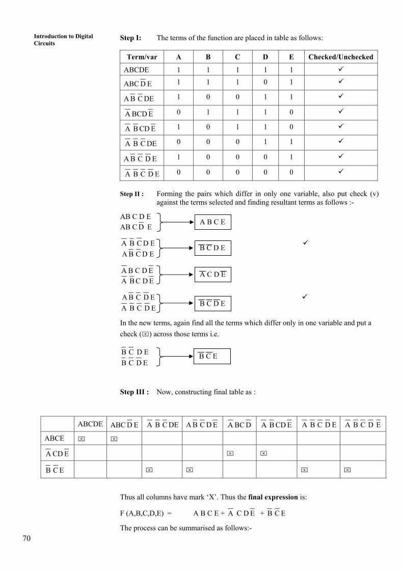
70
Introduction to Digital Circuits
Step I: The terms of the function are placed in table as follows:
Term/var A B C D E Checked/Unchecked
ABCDE 1 1 1 1 1
ABC D E 1 1 1 0 1
A B C DE 1 0 0 1 1
A BCD E 0 1 1 1 0
A B CD E 1 0 1 1 0
A B C DE 0 0 0 1 1
A B C D E 1 0 0 0 1
A B C D E 0 0 0 0 0
Step II : Forming the pairs which differ in only one variable, also put check (v)
against the terms selected and finding resultant terms as follows :-
AB C D E AB C D E
A B C D E A B C D E
A B C D E A B C D E
A B C D E A B C D E
In the new terms, again find all the terms which differ only in one variable and put a check (⌧) across those terms i.e.
B C D E B C E
B C D E
A C D E
B C D E
A B C E
B C D E
Step III : Now, constructing final table as :
ABCDE ABC D E A B C DE A B C D E A BC D A B CD E A B C D E A B C D E
ABCE ⌧ ⌧
A CD E ⌧ ⌧
B C E ⌧ ⌧ ⌧ ⌧
Thus all columns have mark ‘X’. Thus the final expression is:
F (A,B,C,D,E) = A B C E + A C D E + B C E
The process can be summarised as follows:-

71
Principles of Logic Circuits I
Step I : Build a table in which each term of the expression is represented in row (Expression should be in SOP form). The terms can be represented in the
0 (Complemented) or 1 (normal) form.
Step II : Check all the terms that differ in only one variable and then combine the pairs by removing the variable that differs in those terms. Thus a new table is formed.
This process is repeated, if necessary, in the new table also until all uncommon terms are left i.e. no matches left in table.
Step III :
a) Finally, a two dimensional table is formed all terms which are not eliminated in the table form rows and all original terms form the column.
b) At each intersection of row and column where row term is subset of column term, a ‘X’ is placed.
Step IV :
a) Put a square around each ‘X’ which is alone in column b) Put a circle around each ‘X’ in any row which contains a squared
‘X’ c) If every column has a squared or circled ‘X’ then the process is complete
and the corresponding minimal expression is formed by all row terms which have marked Xs.
Check Your Progress 2
1) Prepare the truth table for the following boolean expressions:
(i) A B C + A B C
(ii) (A+B) . ( A + B )
2 Simplify the following functions using algebraic simplification procedures and draw the logic diagram for the simplified function.
(i) F = ( ( A .B) + B )
(ii) F = ( ( A. B) . ( A B ) )
.....................................................................................................................................
…………………………………………………………………………………………
…………………………………………………………………………………………
…………………………………………………………………………………………
…………………………………………………………………………………………
…………………………………………………………………………………………
3) Simplify the following boolean functions in SOP and POS forms by means of
K-Maps.
Also draw the logic diagram.
F (A,B,C,D) = Σ (0,2,8,9,10,11,14,15)
. ....................................................................................................................................
…………………………………………………………………………………………
…………………………………………………………………………………………
…………………………………………………………………………………………

72
Introduction to Digital Circuits 3.5 DESIGN OF COMBINATIONAL CIRCUITS
The digital circuits, which we use now-a-days, are constructed with NAND or NOR gates instead of AND–OR–NOT gates. NAND & NOR gates are called Universal Gates as we can implement any digital system with these gates. To prove this point we need to only show that the basic gates : AND , OR & NOT, can be implemented with either only NAND or with only NOR gate. This is shown in figure 3.9 below:
Figure 3.9 : Basic Logic Operations with NAND and NOR gates
Any Boolean expression can be implemented with NAND gates, by expressing the function in sum of product form.
Example: Consider the function F (A, B, C) = Σ (1,2,3,4,5,7). Firstly bring it in SOP form. Thus, from the K-Map shown in figure 3.10(a), we find
=
++=++=
)BA(.)BA(.C
BABACBABAC)C.B.A(F
Figure 3.10: K-Map & Logic circuit for function F (A, B, C) = Σ (1,2,3,4,5,7).

73
Principles of Logic Circuits I
Similarly, any Boolean expression can be implemented with only NOR gate by expressing in POS form. Let us take same example, F (A, B, C) =Σ (1,2,3,4,5,7).
As discussed in section 3.4.1, the above function F can be represented in POS form as
F (A, B, C) = ∏ (0,6)
( ) ( ) ( ) ( )
+++
++=
++++=++++=
CBACBA
CB.A.CBACBA.CBA
Figure 3.11: Logic circuit for function F (A, B, C) =Σ (1,2,3,4,5,7) using NOR gates
After discussing so much about the design let us discuss some important combinational circuits. We will not go into the details of their design in this unit.
3.6 EXAMPLES OF COMBINATIONAL CIRCUITS
The design of combinational circuits can be demonstrated with some basic combinational circuits like adders, decoders, multiplexers etc. Let us discuss each of these examples briefly. 3.6.1 Adders
Adders play one of the most important roles in binary arithmetic. In fact fixed point addition is often used as a simple measure to express processor’s speed. Addition and subtraction circuit can be used as the basis for implementation of multiplication and division. ( we are not giving details of these, you can find it in Suggested Reading). Thus, considerable efforts have been put in designing of high speed addition and substraction circuits. It is considered to be an important task since the time of Babbage. Number codes are also responsible for adding to the complexity of arithmetic circuit. The 2’s complement notation is one of the most widely used codes for fixed-point binary numbers because of ease of performing addition and subtraction through it.
A combinational circuit which performs addition of two bits is called a half adder, while the combinational circuit which performs arithmetic addition of three bits (the third bit is the previous carry bit) is called a full adder.
In half adder the inputs are:

74
Introduction to Digital Circuits
The augend lets say ‘x’ and addend ‘y’ bits.
The outputs are sum ‘S’ and carry ‘C’ bits. The logical relationship between these are given by the truth table as shown in figure 3.12 (a). Carry ‘C’ can be obtained on applying AND gate on ‘x’ & ‘y’ inputs, therefore , C = x.y, while S can be found from the Karnaugh Map as shown in figure 3.12(b). The corresponding logic diagram is shown in figure 3.12(c).
Thus, the sum and carry equations of half- adder are:
S = x. y + x .y C = x.y
(a) Truth table (b) K- Map for ‘S’
(c ) Logic Diagram
Figure 3.12: Half – Adder implementation
Let us take the full adder. For this another variable carry from previous bit addition is added let us call it ‘p’. The truth table and K-Map for this is shown in figure 3.13.
K – Maps for ‘C’
Truth tableK=Maps for ‘S’

75
Principles of Logic Circuits I
(d) Logic Diagram (e) Block Diagram
Figure 3.13 : Full-adder implementation
Three adjacencies marked a,b,c in K-Map of ‘C’ are
a) x y p + x y p
= x p ( y + y )
= x p
b) x y p + x y p
= x y
c) x y p + x y p = y p
Thus, C = x p + x y + y p
In case of K-Map for ‘S’, there are no adjacencies. Therefore,
S = x y p + x y p + x y p + x y p
Till now we have discussed about addition of bit only but what will happen if we are actually adding two numbers. A number in computer can be 4 byte i.e. 32 bit long or even more. Even for these cases the basic unit is the full adder. Let us see (for example) how can we construct an adder which adds two 4 bit numbers. Let us assume that the numbers are: x3 x2 x1 x0 and y3 y2 y1 y0; here xi and yi (i = 0 to 3) represent a bit. The 4-bit adder is shown in figure 3.14.
Figure 3.14 : 4-bit Adder

76
Introduction to Digital Circuits
The overall sum is represented by S3 S2 S1 S0 and over all carry is C3 from the 4th bit adder. The main feature of this adder is that carry of each lower bit is fed to the next higher bit addition stage, it implies that addition of the next higher bit has to wait for the previous stage addition. This is called ripple carry adder. The ripple carry becomes time consuming when we are going for addition of say 32 bit. Here the most significant bit i.e. the 32nd bits has to wait till the addition of first 31 bits is complete.
Therefore, a high-speed adder, which generates input carry bit of any stage directly from the input to previous stages was developed. These are called carry lookahead adders. In this adder the carry for various stages can be generated directly by the logic expressions such as:
C0 = x0 y0 C1 = x1 y1 + (x1 + y1) C0
The complexity of the look ahead carry bit increases with higher bits. But in turn it produces the addition in a very small time. The carry look ahead becomes increasingly complicated with increasing numbers of bits. Therefore, carry look ahead adders are normally implemented for adding chunks of 4 to 8 bits and the carry is rippled to next chunk of 4 to 8 bits carry look ahead circuit.
Adder- subtractor
The subtraction operation on binary numbers can be achieved by sequence of addition operations only i.e. to perform subtraction, A-B, we can find 2’s complement of B. This can be calculated using 1’s complemented & then adding 1 to it. Thus, a common circuit can perform the addition and subtraction operation. A 4-bit adder- subtraction circuit is shown in figure 3.15, which is formed by using XOR gate with every full adder. The XOR gate with output 0 is for detecting overflow.
Figure 3.15: 4-bit adder-subtractor circuit
The control input ‘x’ controls the operations i.e. if x =0 then the circuit behaves like an adder and if x =1 then circuit behaves like a subtractor. The operation is summarized as :
a) When x = 0, c = 0, the output of all XOR gates will be the same as the corresponding input Bi where i = 0 to 3. Thus, Ai & Bi are added through full adders giving Sum, Si & carry Ci

77
Principles of Logic Circuits I
b) When x = 1, the output of all XOR gates will be complement of input Bi where i =0 to 3, to which carry C0=1 is added. Thus, the circuit finds A plus 2’s complement of B, that is equal to A─B.
3.6.2 Decoders Decoder converts one type of coded information to another form. A decoder has ‘n’ inputs and an enable line (a sort of selection line) and 2n output lines. Let us see an example of 3 8 decoder which decodes a 3 bit information and there is only one output line which gets the value 1 or in other words, out of 2
×3 = 8 lines only 1 output
line is selected. Thus, depending on selected output line the information of the 3 bits can be recognized or decoded.
(a) Block Diagram (b) Logic Diagram
(c) Truth Table
Figure 3.16 : 3×8 decoder
Please make sure while constructing the logic diagram wherever the values in the truth table are appearing as zero in input and one in output the input should be fed in complemented form e.g. the first 4 entries of truth table contains 0 in I0 position and hence I0 value 0 is passed through a NOT gate and fed to AND gates ‘a’, ‘b’, ‘c’ and ‘d’ which implies that these gates will be activated/selected only if I0 is 0. If I0 value is 1 then none of the top 4 AND gates can be activated. Similar type of logic is valid for I1. Please note the output line selected is named 000 or 010 or 111 etc. The output value of only one of the lines will be 1. These 000, 010 indicates the label and suggest that if you have these I0 I1 I2 input values the labeled line will be selected for the output. The enable line is a good resource for combining two 3×8 decoders to make one 4×16 decoder.

78
Introduction to Digital Circuits 3.6.3 Multiplexer
Multiplexer is one of the basic building units of a computer system which in principle allows sharing of a common line by more than one input lines. It connects multiple input lines to a single output line. At a specific time one of the input lines is selected and the selected input is passed on to the output line. The diagram 4×1 multiplexer ( MUX) is given in figure 3.16.
(a) Block diagram (c) Truth table
( c) Logic diagram
Figure 3.17: 4 × 1 Multiplexer
But how does the multiplexer know which line to select? This is controlled by the select lines. The select lines provide the communication among the various components of a computer. Now let us see how the multiplexer also known as MUX works, here for simplicity we will take the example of 4 ×1 MUX i.e. there are 4 input lines connected to 1 output line. For the sake of consistency we will call input line as I, and output line as O and control line a selection line S or enable as E.
Please notice the way in which S0 and S1 are connected in the circuit. To the ‘a’ AND gate S0 and S1 are inputted in complement form that means ‘a’ gate will output I0 when both the selection lines have a value 0 which implies 0S = 1 and 1S = 1, i.e. S0= 0 and S1=0 and hence the first entry in the truth table. Please note that at S0 = 0 and S1 = 0, AND gate ‘b’, ‘c’, ‘d’ will yield 0 output and when all these outputs will pass OR gate ‘e’ they will yield I0 as the output for this case. That is for S0=0 and S1=0 the output becomes I0, which in other words can be said as “ For S0 = 0 and S1 = 0, I0 input line is selected by MUX”. Similarly other entries in the truth table are corresponding to the logical nature of the diagram. Therefore, by having two control lines we could have a 4×1 MUX. To have 8×1 MUX we must have 3 control lines or with 3 control lines we could make 23 = 8 i.e. 8×1 MUX. Similarly, with ‘n’ control lines we can have
2n×1 MUX. Another parameter which is predominant in MUX design is a number of inputs to AND gate. These inputs are determined by the voltage of the gate, which normally support a maximum of 8 inputs to a gate.

79
Principles of Logic Circuits I
Where can these devices used in the computer? The multiplexers are used in digital circuits for data and controlled signal routing.
We have seen a concept where out of ‘n’ input lines, 1 can be selected, can we have a reverse concept i.e. if we have one input line and data is transmitted to one of the possible 2n lines where ‘n’ represents the number of selection lines. This operation is called Demultiplexing.
3.6.4 Encoders An Encoder performs the reverse function of the decoder. An encoder has 2n input lines and ‘n’ output line. Let us see the 8 ×3 encoder which encodes 8 bit information and produces 3 outputs corresponding to binary numbers. This type of encoder is also called octal–to– binary encoder. The truth table of encoder is shown in figure 3.17.
(a) Block diagram
I0 I1 I2 I3 I4 I5 I6 I7 O2 O1 O0 1 0 0 0 0 0 0 0 D0 0 0 0
0 1 0 0 0 0 0 0 D1 0 0 1
0 0 1 0 0 0 0 0 D2 0 1 0
0 0 0 1 0 0 0 0 D3 0 1 1
0 0 0 0 1 0 0 0 D4 1 0 0
0 0 0 0 0 1 0 0 D5 1 0 1
0 0 0 0 0 0 1 0 D6 1 1 0
0 0 0 0 0 0 0 1 D7 1 1 1
(b) Truth Table
Figure 3.18 : Encoder
From the encoder table, it is evident that at any given time only one input is assumed to have 1 value. This is a major limitation of encoder. What will happen when two inputs are together active? The obvious answer is that since the output is not defined the ambiguity exists. To avoid this ambiguity the encoder circuit has input priority so that only one input is encoded. The input with high subscript can be given higher priority. For example, if both D2 and D6 are 1 at the same time, then the output will be 110 because D6 has higher priority then D2.
The encoder can be implimented with 3 OR gates whose inputs can be determined from the truth table. The output can be expressed as:
O0 = I1 + I3 + I5 + I7 O1 = I2 + I3 + I6 + I7 O2 = I4 + I5 + I6 + I7 You can draw the K-Maps to determine above functions and draw the related combinational circuit

80
Introduction to Digital Circuits 3.6.5 Programmable Logic Array
Till now the individual gates are treated as basic building blocks from which various logic functions can be derived. We have also learned about the stratergies of minimization of number of gates. But with the advancement of technology the integration provided by integrated circuit technology has increased resulting into production of one to ten gates on a single chip (in small scale integration). The gate level designs are constructed at the gate level only but if the design is to be done using these SSI chips the design consideration needs to be changed as a number of such SSI chips may be used for developing a logic circuit. With MSI and VLSI we can put even more gates on a chip and can also make gate interconnections on a chip. This integeration and connection brings the advantages of decreased cost, size and increased speed. But the basic drawback faced in such VLSI & MSI chip is that for each logic function the layout of gate and interconnection needs to be designed. The cost involved in making such custom designed is quite high. Thus, came the concept of Programmable Logic Array, a general purpose chip which can be readily adopted for any specific purpose. The PLA are designed for SOP form of Boolean function and consist of regular arrangements of NOT, AND & OR gate on a chip. Each input to the chip is passed through a NOT gate, thus the input and its complement are available to each AND gate. The output of each AND gate is made available for each OR gate and the output of each OR gate is treated as chip output. By making appropriate connections any logic function can be implemented in these Programmable Logic Array.
Figure 319: Programmable Logic Array

81
Principles of Logic Circuits I
The figure 3.18(a) shows a PLA of 3 inputs and 2 outputs. Please note the connectivity points, all these points can be connected if desired. Figure 3.18(b) shows an implementation of logic function:
O0 = I0. I1. I2 + I 0. I 1. I 2 and O1 = I 0. I 1. I 2 + I 0. I 1 through the PLA.
3.6.6 Read-only-Memory (ROM) The read-only-memory is an example of a Programmable Logic Device (PLD) i.e the binary information that is stored within a PLD is specified in some fashion and embedded within the hardware. Thus the information remains even when the power goes.
(a) Block Diagram
b) Logic Diagram of 64-bit ROM
Figure 3.20: ROM Design
Figure 3.19 shows the block diagram of ROM. It consists of ‘k’ input address lines and ‘n’ output data lines. An m ×n ROM is an array of binary cell organised into m (2k = m) words of ‘n’ bits each. The ROM does not have any data input because the write operation is not defined for ROM. ROM is classified as a combinational circuit and constructed internally with decoder and a set of OR gates.
In general, a m × n ROM (where m= 2k, k = no. of address lines) will have an internal k ×2k decoder and ‘n’ OR gate. Each OR gates has 2k inputs which are connected to each of the outputs of the decoder.

82
Introduction to Digital Circuits
Check Your Progress 3
1) Draw a Karnaugh Map for 5 variables.
………………………………………………………………………………..
……………………………………………………………………………….
……………………………………………………………………………….
2) Map the function having 4 variables in a K- Map and draw the truth table. The
funcion is F (A, B, C, D) = (2,6,10,14).
………………………………………………………………………………..
………………………………………………………………………………..
………………………………………………………………………………..
3) Find the optimal logic expression for the above function. Draw the reasultant
logic diagram.
………………………………………………………………………………..
……………………………………………………………………………….
……………………………………………………………………………….
4) What are the advantages of PLA?
……………………………………………………………………………….
……………………………………………………………………………….
……………………………………………………………………………….
5) Can a full adder be constructed using 2 half adders?
………………………………………………………………………………
………………………………………………………………………………
………………………………………………………………………………
3.7 SUMMARY
This unit provides you the information regarding a basis of a computer system. The key elements for the design of a combinational circuit like adders etc. are discussed in this unit. With the advent of PLA’s the designing of circuit is changing and now the scenario is moving towards micro processors. With this developing scenario in the forefront and the expectation of Ultra- Large- Integration (ULSI) in view, time is not far of when design of logic circuits will be confined to single microchip components. You can refer to latest trends of design and development including VHDL (a hardware design language) in the further readings.
3. 8 SOLUTIONS/ANSWERS
Check Your Progress 1
1. Logic gates produce typical outputs based on input values NAND and NOR are universal gates as they can be used to constant any other logic gate.

83
Principles of Logic Circuits I
2.
F =
++
+ BABA
= ( ) ( )BA.BA ++ = ( A + B ) . (A+ B ) = ( A + B ). A + ( A + B ) B = A .A+A B + A . B + B . B = 0 + A B + A B + B = 0 + B (A+ A ) + B = 0 + B + B = B 3. 4.
5.
Check Your Progress 2
1 (i): A B C F= (A B C + A B C )
0 0 0 0 0 0 1 0 0 1 0 1 0 1 1 0

84
Introduction to Digital Circuits
1 0 0 1 1 0 1 0 1 1 0 0 1 1 1 0 (ii)
A B F=(A+B). ( A + B )
0 0 0 0 1 1 1 0 1 1 1 0
2 (i)
F = ( ( A.B ) + B) = + A + B + B = A + 1 (B+ B is always 1) = 1
(ii)
F = ( A.B) . ( A B ) = ( A + B ). ( A B ) = A A B + A B B = A B + A B = A B
3
DACBBAF ++=
( )DACBBAF ++=
F = ( ) ( ) ( )DA.CB.BA F = ( ) ( ) ( )DA.CB.BA +++

85
Principles of Logic Circuits I
Check Your Progress 3 :
1
2 K-Map
Truth table
A B C D F 0 0 0 0 0 0 0 0 1 0 0 0 1 0 1 0 0 1 1 0 0 1 0 0 0 0 1 0 1 0 0 1 1 0 1 0 1 1 1 0 1 0 0 0 0

86
Introduction to Digital Circuits
1 0 0 1 0 1 0 1 0 1 1 0 1 1 0 1 1 0 0 0 1 1 0 1 0 1 1 1 0 1 1 1 1 1 0 3. One adjacency of 4 variables, So
F = C. D
4. PLA’s are generic chips that can be used to implement a number of SOP logic function
5.

87
Principles of Logic Circuits II UNIT 4 PRINCIPLE OF LOGIC CIRCUITS II
Structure Page Nos.
4.0 Introduction 87 4.1 Objectives 87 4.2 Sequential Circuits: The Definition 87 4.3 Flip Flops 88 4.3.1 Basic Flip-Flops 4.3.2 Excitation Tables 4.3.3 Master Slave Flip Flops 4.3.4 Edge Triggered Flip-flops 4.4 Sequential Circuit Design 95 4.5 Examples of Sequential Circuits 98 4.5.1 Registers 4.5.2 Counters – Asynchronous Counters 4.5.3 Synchronous Counters 4.5.4 RAM 4.6 Design of a Sample Counter 103 4.7 Summary 105 4.8 Solutions/ Answers 105
4.0 INTRODUCTION
By now you are aware of the basic configuration of computer systems, how the data is represented in computer systems, logic gates and combinational circuits. In this unit you will learn how all the computations are performed inside the system. You will come across terms like flip flops, registers, counters, sequential circuits etc. Here, you will also learn how to make circuits using combinational and sequential circuits. These circuit design will help you in performing practicals in MCSL-017 lab course.
4.1 OBJECTIVES
After going through this unit you will be able to:
• define the flip-flops and latch;
• describe behaviour of various flip-flops;
• define significance of excitation tables and state diagrams;
• define some of the useful circuits of a computer system like registers counters
etc.; and
• construct logic circuits involving sequential and combinational circuits.
4.2 SEQUENTIAL CIRCUITS: THE DEFINITION
A sequential circuit is an interconnection of combinational circuits and storage elements. The storage elements, called flip-flops, store binary information that indicates the state of sequential circuit at that time. The block diagram of a sequential circuit is shown in figure 4.1.
As shown in the diagram, the present output depends upon the past Input states.

88
Introduction to Digital Circuits
Figure 4.1: Block Diagram of sequential circuits.
These sequential circuits unlike combinational circuits are time dependent. The sequential circuits are broadly classified, depending upon the time at which these are observed and their internal state changes. The two broad classifications of sequential circuits are:
• Synchronous • Asynchronous Synchronous circuits use flip-flops and their status can change only at discrete intervals (Doesn’t it seems as good choice for discrete digital devices such a computers?). Asynchronous sequential circuits may be regarded as combinational circuit with feedback path. Since the propagation delays of output to input are small, they may tend to become unstable at times Thus, complex asynchronous circuits are difficult to design.
The synchronization in a sequential circuit is achieved by a clock pulse generator, which gives continuous clock pulse. Figure. 4.2. shows the form of a clock pulse.
Figure 4.2: Clock signals of clock pulse generator
A clock pulse can have two states: - 0 or 1; disabled or active state. The storage elements can change their state only when a clock pulse occurs. Sequential circuits that have clock pulses as input to flip-flops are called clocked sequential circuit.
4.3 FLIP-FLOPS
Let us see flip-flops in detail. A flip-flop is a binary cell, which stores 1-bit of information. It itself is a sequential circuit. By now we know that flip-flop can change its state when clock pulse occurs but when? Generally, a flip-flop can change its state when the clocks transitions from 0 to 1 (rising edge) or from 1 to 0 (falling edge) and not when clock is 1. If the storage element changes its state when clock is exactly at 1 then it is called latch. In simple words, flip-flop is edge-triggered and latch is level- triggered.

89
Principles of Logic Circuits II 4.3.1 Basic Flip-flops
Let us first see a basic latch. A latch or a flip-flop can be constructed using two NOR or NAND gates. Figure 4.3 (a) shows logic diagram for S-R latch using NOR gates. The latch has two inputs S & R for set and reset respectively. When the output is Q=1 & Q =0, the latch is said to be in the set state. When Q=0 & Q =1, it is the reset state. Normally, The outputs Q & Q are complement of each other. When both inputs are equal to 1 at the same time, an undefined state results, as both outputs are equal to 0.
(a) Logic Diagram (b) Truth Table
Figure. 4.3: SR Latch using NOR gates
Figure 4.3 (b) Shows truth table for S-R latch. Let us examine the latch more closely.
i) Say, initially 1 is applied to S leaving R to 0 at this time. As soon as S=1, the
output of NOR gate ‘b’ goes to 0 i.e. Q becomes 0 and almost immediately Q becomes 1 as both the inputs ( Q & R) to NOR gate ‘a’ become 0. The change in the value of S back to 0 does not change Q as the input to NOR gate ‘b’ now are Q = 1 & S=0. Thus, the flip-flop stays in set state even after S returns to 0.
ii) If R goes to 1 then latch acquires clear state. On changing R to 1, Q changes to
0 irrespective of the state of flip-flop and as Q is 0 & S is 0 then Q becomes 1. Even after R returns to 0, Q remains 0 i.e. latch is in clear state.
iii) When both S & R go to 1 simultaneously, the two outputs go to 0. This gives
undefined state. Let us try to construct most common flip- flops from this basic latch. R-S Flip flop - The graphic symbol of S-R flip-flop is shown in Fig 4.4. It has three inputs, S (set), R (reset) and C (for clock). The Q(t+1) is the next state of flip-flop after the occurrence of a clock pulse. Q(t) is the present state, that is present Q value (Set-1 or Reset– 0).
(a) Graphic Symbol

90
Introduction to Digital Circuits
(b) Logic Diagram
(c) Characteristic Table
Figure 4.4: R-S Flip-flop
In figure 4.4 (a), the arrowhead symbol in front of clock pulse C indicates that the flip-flop responds to leading edge (from 0 to 1) of input clock signal. Operation of R-S flip-flop can be summarised as:
1) If no clock signal i.e. C=0 then output can not change irrespective of R & S values
2) When clock signal changes from 0 to 1 and S=1, R=0 then output Q=1 & Q =0 (Set)
3) If R=1 S=0 & clock signal C changes from 0 to 1 then output Q=0 & Q =1 (Reset)
4) During positive clock transition if both S & R become 1 then output is not defined, as it may become 0 or 1 depending upon internal timing delays occurring in circuit.
D Flip -Flop
The D (data) flip-flop is modification of RS flip-flop. The problem of undefined output in SR flip-flop when both R & S become 1 gets avoided in D flip-flop. The simple solution to avoid such condition is by providing just a single input. Thus, the non-clocked inputs to AND gates (S &R of fig 4.4 (b)) are guaranteed to be opposite of each other by inserting an inverter between them. The logic diagram and characteristic table of D flip flop is shown in figure 4.5.
(a) Graphic Symbol (b) Logic Diagram (c) Characteristic Table
Figure 4.5: D Flip flop
91
Principles of Logic Circuits II
D flip-flop is also referred as Delay flip-flop because it delays the 0 or 1 applied to its input by a single clock pulse.
J-K flip-flop
The J-K flip-flop is also a modification of SR flip-flop, it has 2 inputs like S & R and all possible inputs combinations are valid in J K flip-flop.
Figure. 4.6 shows implementation of J K flip-flop. The inputs J & K behave exactly like input S & R to set and reset flip-flop, respectively. When J & K are 1, the flip- flop output is complemented with clock transition. [Try this as an exercise]
(a) Graphic Symbol (b) Logic Diagram (c) Characteristic Table
Figure 4.6: J – K Flip flop
T flip-flop
T (Toggle) flip-flop is obtained from JK flip-flop by joining inputs J &K together. The implementation of T flip-flop is shown in figure. 4.7. When T=0, the clock pulse transition does not change the state. When T=1, the clock pulse transition complement the state of the flip-flop.
(a) Graphic Symbol b) Logic Diagram
(c) Characteristic Table
Figure 4.7: T- Flip flop

92
Introduction to Digital Circuits 4.3.2 Excitation Tables
The characteristic tables of flip-flops provide the next state when inputs and the present state are known. These tables are useful for analysis of sequential circuits. But, during the design process, we know the required transition from present state to next state and wish to find the required flip-flop inputs. Thus comes the need of a table that lists the required input values for given change of state. Such a table is called excitation Table. Fig 4.8 shows excitation tables for all flip-flops.
Q(t) Q(t+1) J K Q((t) Q(t+1) S R
0 0 0 X 0 0 0 X
0 1 1 X 0 1 1 0
1 0 X 1 1 0 0 1
1 1 X 0 1 1 X 0
(a) J-K Flip flop (b) S-R Flip flop
Q(t) Q(t+1) D Q(t) Q(t+1) T
0 0 0 0 0 0
0 1 1 0 1 1
1 0 0 1 0 1
1 1 1 1 1 1
(c) D Flip flop (d) T Flip flop
Figure 4.8: Excitation Tables for flip-flops
Q(t) & Q(t+1) indicates present and next state for flip a flop, respectively. The symbol X in the table means don’t care condition i.e. doesn’t matter whether input is 0 or 1.
Let us discuss more deeply, how these excitation tables are formed. For this, we take an example of J-K Flip flop.
1) The state transition from present state 0 to next state 0 (Figure 408 (a) can be achieved when
(a) J=0, K=0, then no change in the state of flip flop
(b) J=0, K=1, then flip flop resets i.e. 0
(remember J-K Characterstic table from figure 4.6)
Thus in either case J=0 but K can be 0 or 1 that is represented by don’t care condition X.
2) The state transition from present state 0 to next state 1 can be achieved when
(a) J=1, K=0, then flip flop is set i.e. 1
(b) J=1, K=1, then flip flop is complemented i.e.change from 0 to 1
Here, also in either case J=1 but K can be 0 or1 that means again K is represented as a don’t care case.
3) Similarly, state transition from present state 1 to next state 0 can be achieved when
(a) J=0, K=1, flip flop is reset i.e.0
(b) J=1, K=1, flip flop is complemented i.e. changes from 1 to 0

93
Principles of Logic Circuits II
This indicates that in either case K=1 but J can be either 0 or 1 thus don’t care case.
4) For state transition from present state 1 to next state 1 can be achieved when
(a) J=0, K=0, no change in flip flop
(b) J=1, K=0, flip flop is set i.e 1
Thus J is don’t care case but K=0.
This whole process can be summarized in the table below:
Present State Next State Can be achieved 0 0 a) J=0, K=0, since Q (t) =0
b) J=0, K=1, flip flop resets
0 1 a) J=1, K=0, flip flop set
b) J=1, K=1, flip flop complements, Q (t) =0=Q (t+1) =1
1 0 a) J=0, K=1, flip flop reset
b) J=1, K=1, complement Q (t)= )t(Q
1 1 a) J=0, K=0, no change
b) J=1, K=0, flip – flop set
Similarly, the excitation tables for the rest of the flip-flops can be derived (Try to do this as an exercise).
Check Your Progress 1
1. What are sequential circuits?
.....................................................................................................................................
.....................................................................................................................................
…………………………………………………………………………………………
…………………………………………………………………………………………
2. What is flip- flop? How is different from latch? .....................................................................................................................................
.....................................................................................................................................
…………………………………………………………………………………………
…………………………………………………………………………………………
3. What is the difference between excitation table and characteristic table?
.....................................................................................................................................
.....................................................................................................................................
…………………………………………………………………………………………
4.3.3 Master-Slave Flip-Flop
The master slave flip-flop consists of two flip-flops. One is the master flip-flop & other is called the slave flip-flop. Fig 4.9 shows implementation of master-slave flip-flop using J-K flip-flop.

94
Introduction to Digital Circuits
Note: Master-slave flip-flopmanner.
Now, let us summarize the wo
(i) When the clock pulsebecomes active and itrespectively. Why? Ware either Y=1, Y =0 following combinatio
(a) J=1, K=0 (b) J=0, K=1
(ii) When inputs are applieactivated resulting in inthe input and previousmaintaining its previoubecomes inactive and sland (b) conditions abov
But why do we require this msituation where output of one assumption is that clock pulsesame time. The change of statduring that time the output of flops in the system can be chathough output of flip-flops are
4.3.4 Edge-Triggered
An edge-triggered flip-flop is pulse transition instead of conrising edge (0 to 1 transition) transition). Fig 4.10 shows thtriggered flip-flops.
Figure 4.9: Master – Slave flip- flop
can be constructed using D or SR flip-flop in the same
rking of this flip-flop:
is 0, the master flip-flop is disabled but the slave ’s output Q & Q becomes equal to Y and Y ell the possible combination of the value of Y and Y’ or Y=0 Y =1. Thus, the slave flip-flop can have ns: -
which means Q=1, Q =0 (stet flip-flop) which means Q=0, Q =1 (clear flip-flop)
d at JK and clock pulse becomes 1, only master gets termediate output Y going to state 0 or 1 depending on state. Remember that during this time slave is also s state only. As the clock pulse becomes 0, the master ave acquires the same state as master as explained in (a) e.
aster-slave combination? To understand this, consider a flip-flop is going to be input of other flip-flop. Here, the inputs of all flip-flops are synchronized and occur at the e of master occurs when the clock pulse goes to 1 but slave still has not changed, thus the state of the flip-nged simultaneously during the same clock pulse even connected to the inputs of other flip-flops.
flip-flops
used to synchronize the state change during a clock stant level. Some edge-triggered flip-flops trigger on the whereas others trigger on the falling edge (1- to 0 e clock pulse signal in positive & negative edge-

Principles of Logic Circuits II
Output can not Output change cannot
Positive … change Transition Negative
Transition (a) Pulse in positive edge-triggered flip-flop (b) Pulse in Negative edge-triggered flip flop
Figure. 4.10: Pulse signal
O
(a) Po riggered D flip-flop (b) Negative edge–triggered D flip-flop
The ewhichtransinot ch
Chec
1.
2.
4.4
A seqand into desmakin
Let ufunctnext)In stabetwelabellinputstate.
The f
CC
D Q
sitive edge-t
Figure 4.11: Edge triggered D flip
ffective positive clock transition include the D input must be maintained at constion. Similarly, a minimum time called hange after the application of positive tra
k Your Progress 2
What are the advantages of master- slav
....................................................................
....................................................................
What are edge- triggered flip-flops?
....................................................................
....................................................................
SEQUENTIAL CIRCU
uential circuit is specified by a time seqternal flip-flop binary states. Thus firstlcribe behaviour of the circuit. Then fromg logic circuit diagram.
s first see what is state table and state diaional relationships between the inputs, o of a sequential circuit. A state diagram pte diagram, a circle describes a state anden states. The state of flip-flop is writtened with two binary numbers separated b value during present state and second nu The state diagram of a binary counter is
ollowing is the procedure for design of s
D Q
95
- flops
s a minimum time called setup time, for tant value before the occurrence of clock old time, for which the D input must nsition of the pulse.
e flip-flop?
.................................................................
.................................................................
.................................................................
.................................................................
IT DESIGN
uence of external inputs, external outputs y, a state table and state diagram is used the state table, we get information for
gram. A state table includes the utput and flip-flop states (present and ictorially describes the state transition. directed lines indicate the transition inside the circle. The directed lines are
y a slash. The first one indicates the mber indicates output during present given in figure 4.12 (b).
equential circuits:

96
Introduction to Digital Circuits
1) Draw state table or state diagram from the problem statement, (if state diagram is available, draw state table also)
2) Give binary codes to states. 3) From state table, make input equation in simplified form. i.e. generating
Boolean functions which describes signals for the inputs of flip-flops. 4) From state table, derive output equation in simplified form. 5) Draw logic diagram with required flip-flops and combinational circuits. Let us take an example to illustrate the above procedure. Suppose we want to design 2-bit binary counter using D flip-flop. The circuit goes through repeated binary states 00, 01, 10 and 11 when external input X = 1 is applied. The state of circuit will not change when X = 0. The state table & state diagram for this is shown in figure 4.12. But how do we make this state diagram? Please note the number of flip-flops– 2 in our example as we are designing 2 bits counter. Various states of two bit input would be 00 01 10 and 11. These are shown in circle. The arrow indicate the transitions on an input value X. For example, when the counter is in state 00 and input value X=0 occurs, the counter remains in 00 state. Hence the loop back on X= 0. However, on encountering X=1 the counter moves to state 01. Like wise in all other states similar transition occur. For making state table remember the excitation table of D flip-flop given in figure 4.8 (c). The present state of the two flip-flops and next states of the flip-flops are put into the table along with any input value. For example, if the present state of flip-flops is 01 and input value is 1 then counter will move to state 10. Notice these values in the fourth row of the values in the state table (figure 4.12 (a) Or we can write as A B A (Next) B (Next) 0 1 X =1 1 0
This implies that flip-flop. A has moved from state clear to set. As we are making the counter using D flip-flop, the question is what would be the input DA value of A flip-flop that allows this transition that is Q(t) = 0 to Q(t+1) =1 possible for A flip flop. On checking the excitation table for D Flip-flop, we find the value of D input of A flip-flop (called DA in this example) would be 1. Similarly, the B flip-flop have a transition Q(t) = 1 to Q(t+1)=0, thus, DB, would be 0. Hence notice the values of flip-flop inputs DA and DB. (Row 3).
a) State Table (b) State Diagram
Figure 4.12: Binary Counter Design
Next step indicates simplification of input equation to flip-flop which is done using K-Maps as shown in fig 4.13. But why did we make K-map for DA or DB which happens to be flip-flop input values? Please note in sequential circuit design, we are

97
Principles of Logic Circuits II
designing the combinational logic that controls the state transition of flip-flops. Thus, each input to a flip-flop is one output of this combinational logic and the present state of flip-flops and any other input value form the input values to this combinational logic.
Figure 4.13: Maps for combinational circuit of 2-bit counter
Thus, two simplified flip–flop input equations are derived:
DA = A B + A X + A BX
DB = B X + B X
The logic diagram is drawn in fig 4.14.
Figure 4.14: Logic diagram for 2-bit Binary Counter

98
Introduction to Digital Circuits
Note: Similarly, the sequential circuits can be designed using any number of flip-flops using state diagrams and combinational circuits design methods.
4.5 EXAMPLES OF SEQUENTIAL CIRCUITS
Let us now discuss some of the useful examples of sequential circuits like registers, counters etc.
4.5.1 Registers
A register is a group of flip-flops, which store binary information, and gates, which controls when and how information is transferred to the register. An n-bit register has n flip-flops and stores n-bits of binary information. Two basic types of registers are: parallel registers and shift registers.
A parallel register is one of the simplest registers, consisting of a set of flip-flops that can be read or written simultaneously. Fig. 4.15 shows a 4-bit register with parallel input-output. The signal lines Io to I3 inputs to flip-flops, which may be output of other arithmetic circuits like multipliers, so that data from different sources can be loaded into the register. It has one additional line called clear line, which can clears the register completely. This register is called a parallel register as all the bits of the register can be loaded in a single clock pulse.
Figure 4.15: 4-bit parallel register
A shift register is used for shifting the data to the left or right. A shift register operates in serial input-output mode i.e. data is entered in the register one bit at a time from one end of the register and can be read from the other end as one bit at a time. Fig. 4.16 shows a 4-bit right shift register using D logical shift functions.
Figure 4.16: 4-bit right – shift register

Principles of Logic Circuits II
Please note that in this re ister signal shift enable is used instead of clock pulse, why? Because it is not necess y that we want the register to perform shift on each clock pulse.
A register, which shifts dregister and a register, wshift register. Shift regisinput-output. A general sfrom the register along wrequire additional controdesired and left or right s4.17 for this register.
There are 3 main controactive, parallel input-ouselect line for selecting rand for value 1, left shift
Figure. 4
4.5.2 Counters A
A counter is a register, wclock pulse is applied. Inthe capacity of register ivalue, the next incremecircuits of digital systemexample, in CPU we hav
Counters can be classifieAsynchronous and synchstate of one flip-flop triggfaster because the state o
Asynchronous Counterchange, which occurs in end to the other. Fig 4.18flip-flops. This counter iscounts from 0000 to 1111
gar
99
ata only in one direction, is called uni-directional shift hich can shift data in both directions, is called bi-directional ter can be constructed for bi-directional shift with parallel hift register structure may have parallel data transfer to or ith added facility of left or right shift. This structure will l lines for indicating whether parallel or serial output is hift is required. A general symbolic diagram is shown in Fig.
l lines shown in the above figure. If parallel load enable is tput operation is done otherwise serial input- output shift ight or left shift. If it has value 0 then right shift is performed is done. Shift enable signal indicates when to start shift.
.17: 4 – bit left shift register with parallel load
synchronous Counters
hich goes through a predetermined sequence of states when principle, the value of counters is incremented by 1 module .e. when the value stored in a counter reaches its maximum nted value becomes zero. The counters are mainly used in s where sequence and control operations are performed, for e program counter (PC).
d into two categories, based on the way they operate: ronous counters. In Asynchronous counters, the change in ers the other flip-flops. Synchronous counters are relatively
f all flip-flops can be changed at the same time.
s : This is more often referred to as ripple counter, as the order to increment the counter ripples through it from one shows an implementation of 4-bit ripple counter using J-K incremented on the occurrence of each clock pulse and (i.e. 0 to 15).

100
Introduction to Digital Circuits
Figure. 4.18: 4 – bit ripple counter
The input line to J & K of all flip-flops is kept high i.e. logic1. Each time a clock pulse occurs the value of flip-flop is complemented (Refer to characteristic table of J K flip-flop in Figure. 4.6 (c). Please note that the clock pulse is given only to first flip-flop and second flip-flop onwards, the output of previous flip-flop is fed as clock signal. This implies that these flip-flops will be complemented if the previous flip-flop has a value 1. Thus, the effect of complement will ripple through these flip-flops.
4.5.3 Synchronous Counters
The major disadvantage of ripple counter is the delay in changing the value. How? To understand this, take an instance when the state of ripple counter is 0111. Now the next state will be 1000, which means change in the state of all flip-flops. But will it occur simultaneously in ripple counter? No, first O0 will change then O1, O2 & lastly O3. The delay is proportional to the length of the counter. Therefore, to avoid this disadvantage of ripple counters, synchronous counters are used in which all flip-flops change their states at same time. Fig 4.19 shows 3-bit synchronous counter.
Figure 4.19: Logic diagram of 3-bit synchronous counter
You can understand the working of this counter by analyzing the sequence of states (O0, O1, O2) given in Figure 4.20
O2 O1 O0
0 0 0 0 1 1 1 1 0
0 0 1 1 0 0 1 1 0
0 1 0 1 0 1 0 1 0
Figure. 4.20 : Truth table for 3 bit synchronous counter

101
Principles of Logic Circuits II
The operation can be summarized as: -
i) The first flip-flop is complemented in every clock cycle
ii) The second flip-flop is complemented on occurrence of a clock cycle if
the current state of first flip-flop is 1.
iii) The third flip-flop is fed by an AND gate which is connected with output of first
and second flip-flops. It will be complemented only when first & second flip-
flops are in Set State.
4.5.4 RAM (Random Access Memory)
Here we will confine our discussion, in general to the RAM only as an example of sequential circuit. A memory unit is a collection of storage cells or flip flops alongwith associated circuits required to transfer information in and out of the device. The access time and cycle time it takes are constant and independent of the location, hence the name random access memory.
(a) Block Diagram (b) Logic Diagram
Figure 4.21: Binary Cell
RAMs are organized (logically) as words of fixed length. The memory communicates with other devices through data input and output lines, address selection lines and control lines that specify the direction of transfer.
Now, let us try to understand how data is stored in memory. The internal construction of a RAM of ‘m’ words and ‘n’ bits per word consists of m ×n binary cells and associated circuits for dectecting individual words. Figure 4.21 shows logic diagram and block digram of a binary cell.
The input is fed to AND gate ‘a’ in complemented form. The read operation is indicated by 1 on read/ write signal. Therefore during the read operation only the ‘AND’ gate ‘c’ becomes active. If the cell has been selected, then the output will become equal to the state of flip flop i.e. the data value stored in flip flop is read. In write operation ‘a’ & ‘b’ gates become active and they set or clear the J-K flip flop depending upon the input value. Please note in case input is 0, the flip flop will go to clear state and if input is 1, the flip flop will go to set state. In effect, the input data is

102
Introduction to Digital Circuits
reflected in the state of flip-flop. Thus, we say that input data has been stored in flip-flop or binary cell.
Fig 4.22 is the extension of this binary cell to an IC RAM circuit, where a 2×4 decoder is used to select one of the four words. (For 4 words we need 2 address lines) Please note that each decoder output is connected to a 4bit word and the read/write signal is given to each binary cell. Once the decoder selects the word, the read/write input tells the operation. This is derived using an OR gate, since all the non-selected cells will produce a zero output. When the memory select input to decoder is 0, none of the words is selected and the contents of the cell are unchanged irrespective of read/write input.
Figure 4.22: 4 × 4 RAM

103
Principles of Logic Circuits II
After discussing so much about combinational circuits and sequential circuits, let us discuss in the next section an example having a combination of both circuits.
4.6 DESIGN OF A SAMPLE COUNTER
Let us design a synchronous BCD counter. A BCD counter follows a sequence of ten states and returns to 0 after the count of 9. These counters are also called decade counters. This type of counter is useful in display applications in which BCD is required for conversion to a decimal readout. Fig 4.23 shows the characteristic table for this counter.
Present State Next State Flip-Flops Inputs A B C D A B C D JA KA JB KB JC KC JD KD
0 0 0 0 0 0 0 1 0 X 0 X 0 X 1 X
0 0 0 1 0 0 1 0 0 X 0 X 1 X X 1
0 0 1 0 0 0 1 1 0 X 0 X X 0 1 X
0 0 1 1 0 1 0 0 0 X 1 X X 1 X 1
0 1 0 0 0 1 0 1 0 X X 0 0 X 1 X
0 1 0 1 0 1 1 0 0 X X 0 1 X X 1
0 1 1 0 0 1 1 1 0 X X 0 X 0 1 X
0 1 1 1 1 0 0 0 1 X X 1 X 1 X 1
1 0 0 0 1 0 0 1 0 X 0 X 0 X 1 X
1 0 0 1 0 0 0 0 0 X 0 X 0 X X 1
Figure 4.23: Characteristic table for decade counter
[NOTE : Remember excitation table for J-K flip flop given in fig 4.8]
There are 4 flip-flop inputs for decade counter i.e. A, B, C, D. The next state of flip-flop is given in the table. JA & KA indicates the flip flop input corresponding to flip-flop-A. Please note this counter require 4-flip-flops.
From this the flip flop input equations are simplified using K-Maps as shown in figure 4.24. The unused minterms from 1010 through 1111 are taken as don’t care conditions.

104
Introduction to Digital Circuits
Figure 4.24: K-maps for Decade counter
Thus, the simplified input equation for BCD counter are:
JA = BCD KA = D JB = CD KB = CD
JC = A D KC = D JD = 1 KD = 1 The logic circuit can be made with 4 JK flip flops & 3 AND gates
Figure 4.25: Logic Diagram for decade counter.

105
Principles of Logic Circuits II Check Your Progress 3
1) Differentiate between synchronous & asynchronous counters? .....................................................................................................................................
.....................................................................................................................................
.....................................................................................................................................
2) Can ripple counter be constructed from a shift register?
.....................................................................................................................................
.....................................................................................................................................
.....................................................................................................................................
3) Can we design a counter with the following repeated binary sequence: 0,1,2,3,4,5,6. If yes, design it using J K flip flop.
.....................................................................................................................................
.....................................................................................................................................
.....................................................................................................................................
4.7 SUMMARY
As told to you earlier this unit provides you information regarding sequential circuits which is the foundation of digital design. Flip-flops are basic storage unit in sequential circuits are derived from the latches. The sequential circuit can be formed using combinational circuits (discussed in the last unit) and flip flops. The behavior of sequential circuit can be analyzed using tables & state diagrams.
Registers, counters etc. are structured sequential blocks. This unit has outlined the construction of registers, counters, RAM etc. Lastly, we discussed how a circuit can be designed using both sequential & combinational circuits. For more details, the students can refer to further reading.
4.8 SOLUTIONS / ANSWERS
Check Your Progress 1
1) An interconnection of combinational circuits and flip-flops, used for making different logic devices in computers that involves manipulation and storage of data. Some such circuits are registers, counters etc.
2) Flip flop is the basic storage element for synchronous sequential circuits.
Whereas latches are bistable devices whose state normally depends upon the asynchronous inputs and are not suitable for use in synchronous sequential circuits using single clock.
3) Excitation table indicates that if present and next state are known then what will
be inputs whereas a characteristics table indicates just opposite of this i.e. inputs are known the, next state has to be found.
Check Your Progress 2
1) The main advantage is that they allow feed back paths
2) Edge-Triggered flip-flops are bi-stable devices with synchronous inputs whose state depends on the inputs only at the triggering transition of a clock pulse i.e. changes in output occur only at triggering transition of the clock
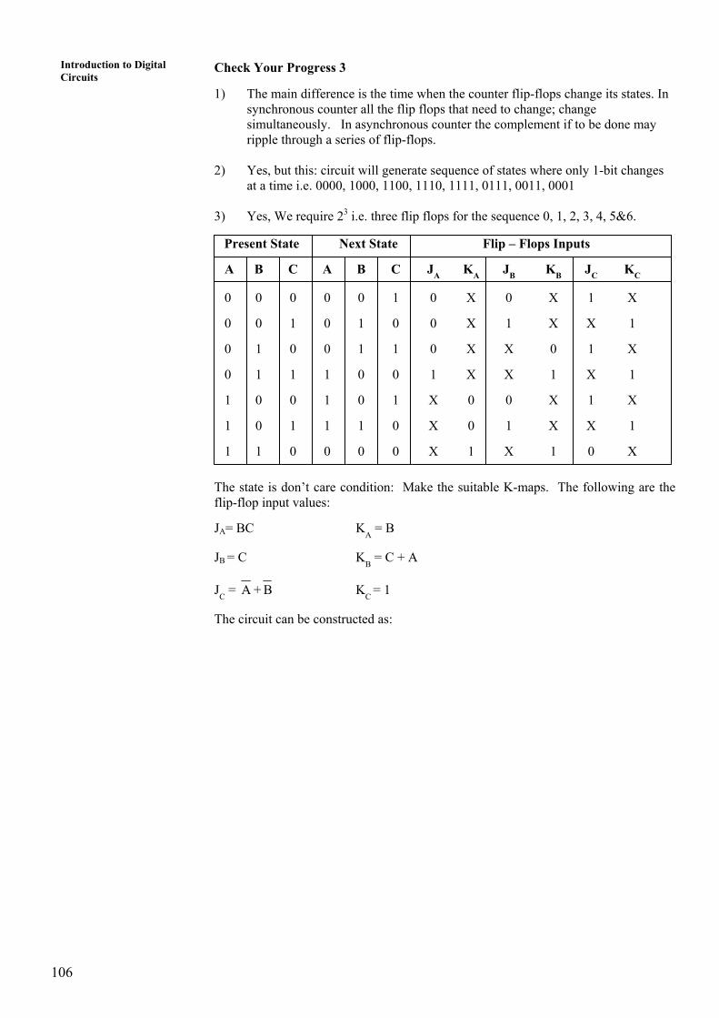
106
Introduction to Digital Circuits
Check Your Progress 3
1) The main difference is the time when the counter flip-flops change its states. In synchronous counter all the flip flops that need to change; change simultaneously. In asynchronous counter the complement if to be done may ripple through a series of flip-flops.
2) Yes, but this: circuit will generate sequence of states where only 1-bit changes
at a time i.e. 0000, 1000, 1100, 1110, 1111, 0111, 0011, 0001 3) Yes, We require 23 i.e. three flip flops for the sequence 0, 1, 2, 3, 4, 5&6.
Present State Next State Flip – Flops Inputs
A B C A B C JA KA JB KB JC KC
0 0 0 0 0 1 0 X 0 X 1 X
0 0 1 0 1 0 0 X 1 X X 1
0 1 0 0 1 1 0 X X 0 1 X
0 1 1 1 0 0 1 X X 1 X 1
1 0 0 1 0 1 X 0 0 X 1 X
1 0 1 1 1 0 X 0 1 X X 1
1 1 0 0 0 0 X 1 X 1 0 X
The state is don’t care condition: Make the suitable K-maps. The following are the flip-flop input values:
JA= BC KA = B
JB = C KB = C + A
JC = A + B KC = 1
The circuit can be constructed as: