Embed Size (px)
Citation preview

MCU Bootloader QuadSPI User's Guide
NXP Semiconductors Document Number: MBOOTQSPIUG
User's Guide Rev 2, 05/2018

Contents
Chapter 1 Introduction....................................................................................4
Chapter 2 Overview.........................................................................................52.1 Terminology......................................................................................................................... 52.2 Requirements...................................................................................................................... 6
2.2.1 Hardware requirements.........................................................................................................62.2.2 Host tools..............................................................................................................................62.2.3 Demo application..................................................................................................................62.2.4 Required toolchains.............................................................................................................. 6
2.2.4.1 Firmware project..................................................................................................................... 62.2.4.2 Host project.............................................................................................................................7
2.3 QuadSPI image boot procedure.......................................................................................... 72.3.1 Plaintext QuadSPI image boot flow...................................................................................... 72.3.2 Encrypted QuadSPI image boot flow....................................................................................7
Chapter 3 Creating application for QuadSPI memory................................. 93.1 Starting point: Basics of internal flash memory mapped led-demo example project........... 93.2 Changes to the led-demo project.......................................................................................10
3.2.1 Changes to the linker file.....................................................................................................103.2.2 Changes to flash config area...............................................................................................113.2.3 Configure BCA.................................................................................................................... 11
3.3 Generate QCB................................................................................................................... 133.3.1 The QCB structure..............................................................................................................133.3.2 Example QCB for MX25U3235F device on TWR-K80F150M Tower System module.........213.3.3 Generate the QCB with a simple example project.............................................................. 24
Chapter 4 Configure QuadSPI with MCU bootloader.................................284.1 Configure QuadSPI at runtime...........................................................................................284.2 Configure QuadSPI at start-up.......................................................................................... 29
Chapter 5 Flash QuadSPI image via SB file................................................315.1 Brief introduction of SB file................................................................................................ 315.2 Generate SB file for QuadSPI image.................................................................................315.3 Flash QuadSPI image via MCU bootloader.......................................................................33
Chapter 6 Advanced Usage: Encrypted QuadSPI image...........................356.1 Generate an SB file with KEK and SB KEY.......................................................................366.2 Generate an SB file with encrypted QuadSPI image.........................................................37
6.2.1 The KeyBlob Block..............................................................................................................386.2.2 Encrypt QuadSPI image..................................................................................................... 386.2.3 Encrypting SB file with the SB key......................................................................................39
Chapter 7 Change QuadSPI clock in QuadSPI image................................417.1 Create a RAM function via IAR EWARM............................................................................41
Contents
MCU Bootloader QuadSPI User's Guide, Revision 2, May 20182 NXP Semiconductors

7.2 Create a RAM function via Keil MDK..................................................................................427.3 Create a RAM function with MCUXpresso IDE.................................................................. 437.4 Ensure no timing issue after clock change......................................................................... 45
Chapter 8 Application running on QuadSPI alias area.............................. 468.1 Create an application to run on QuadSPI Alias Area.........................................................468.2 Create a simple boot application....................................................................................... 488.3 Downloading application running on QuadSPI alias memory with SB file.........................518.4 Creating encrypted QuadSPI application running on QuadSPI Alias memory with SB file52
Chapter 9 Appendix A - QuadSPI configuration procedure...................... 54
Chapter 10 Appendix B - Re-enter MCU bootloader under direct bootmode........................................................................................................... 55
Chapter 11 Appendix C - Explore more features in QCB...........................5611.1 Parallel mode....................................................................................................................5611.2 Continuous read mode..................................................................................................... 58
Chapter 12 Appendix D - DDR mode issue workaround............................6012.1 Example QCB for QuadSPI device N25Q256A with DDR mode support........................6012.2 Example QCB for QuadSPI device S26KS128S with Octal DDR mode support.............6112.3 Changes to user application for implementing DDR mode path...................................... 63
12.3.1 Workaround solution......................................................................................................... 6312.3.2 Changes to linker file........................................................................................................ 6412.3.3 Changes to startup file......................................................................................................6512.3.4 Changes to system_MK82F25615.c file............................................................................65
12.4 Workaround block diagram.............................................................................................. 6712.5 BD file for downloading QuadSPI image under DDR mode.............................................68
Chapter 13 Revision history.........................................................................70
Contents
MCU Bootloader QuadSPI User's Guide, Revision 2, May 2018NXP Semiconductors 3
Chapter 1Introduction
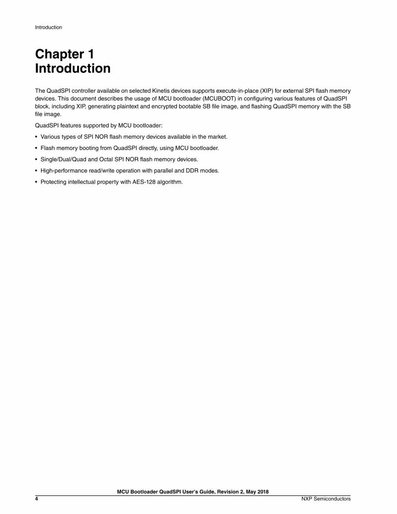
The QuadSPI controller available on selected Kinetis devices supports execute-in-place (XIP) for external SPI flash memorydevices. This document describes the usage of MCU bootloader (MCUBOOT) in configuring various features of QuadSPIblock, including XIP, generating plaintext and encrypted bootable SB file image, and flashing QuadSPI memory with the SBfile image.
QuadSPI features supported by MCU bootloader:
• Various types of SPI NOR flash memory devices available in the market.
• Flash memory booting from QuadSPI directly, using MCU bootloader.
• Single/Dual/Quad and Octal SPI NOR flash memory devices.
• High-performance read/write operation with parallel and DDR modes.
• Protecting intellectual property with AES-128 algorithm.
Introduction
MCU Bootloader QuadSPI User's Guide, Revision 2, May 20184 NXP Semiconductors

Chapter 2Overview
This document mainly focuses on the following topics:
• QuadSPI image boot procedure
• Creating an application image running on QuadSPI memory
• Configuring QuadSPI with MCU bootloader
• Programming QuadSPI memory with SB file
• Advanced usage: QuadSPI encrypted boot image
• Application requirements for re-configuring QuadSPI clock
In addition, the following topics are also covered in the appendix sections:
• QuadSPI configuration block (QCB)
• Re-enter MCU bootloader under direct boot mode
• Explore features supported in QCB
• Working around ROM issues in supported DDR mode devices
2.1 TerminologyThe following table summarizes the terms and abbreviations included in this user's guide.
Table 1. Terminology and abbreviations
Terminology Description
MCUBOOT MCU bootloader
BCA Bootloader Configuration Area, which provides customization of bootloaderoptions, such as enabledPeripherals, peripheralDetectionTimeout, and so on.
See the MCU bootloader chapter in the silicon's reference manual for more details.
QCB QuadSPI Configuration Block, a structure containing configurable parametersneeded by the MCU bootloader to configure the QuadSPI controller.
See the MCU bootloader chapter in the silicon's reference manual for more details.
KeyBlob A data structure which holds the KeyBlob entries. Each keyblob entry defines theencrypted QuadSPI memory region, decryption key, and so on.
See the MCU bootloader chapter in the silicon's reference manual for more details.
KEK KeyBlob Encryption Key, an AES-128 key used for encrypting plaintext KeyBloband decrypting encrypted KeyBlob.
See the MCU bootloader chapter in the silicon's reference manual for more details.
Table continues on the next page...
Overview
Terminology
MCU Bootloader QuadSPI User's Guide, Revision 2, May 2018NXP Semiconductors 5

Table 1. Terminology and abbreviations (continued)
Terminology Description
SB file The SB file is the NXP binary file format for bootable images. The file consists ofsections and sequence of bootloader commands and data that assists MCUbootloader in programming the image to target memory. The image data in theSB file can be encrypted as well. The file can be downloaded to the target usingthe MCU bootloader receive-sb-file command.
See the MCU bootloader chapter in silicon's reference manual for more details
OTFAD On-the-fly AES Decryption is a powerful IP block in MK81F256 and MK82F256,which supports decryption of the encrypted QuadSPI image on-the-fly usingKeyBlob.
See the MCU bootloader chapter in the silicon's reference manual for more details
2.2 Requirements
2.2.1 Hardware requirements• TWR-K80F150M Tower System module
• FRDM-K82F Freedom Development platform
• TWR-KL82 Tower System module
• FRDM-KL82 Freedom Development platform
2.2.2 Host toolsThe following host tools are available with the release package. They assist in generating and provisioning of QuadSPIbootable image for the target device.
• blhost: command line host tool for MCU bootloader.
• elftosb: command line host tool for SB file generation.
• KinetisFlashTool: GUI host tool for MCU bootloader.
2.2.3 Demo applicationLed_demo running in internal flash and QuadSPI memory, under <sdk_package>/boards/<board>/bootloader_examples/demo_apps
QCBGenerator, under <sdk_package>/middleware/mcu-boot/apps/QCBGenerator/build
2.2.4 Required toolchains2.2.4.1 Firmware projectThe following toolchains can be used to build the example led_demo firmware application provided with the release package.
• ARM® Keil
® development tool v5.24a with corresponding device pack
• IAR Embedded Workbench for ARM® v8.20.2
Overview
Requirements
MCU Bootloader QuadSPI User's Guide, Revision 2, May 20186 NXP Semiconductors

• MCUXpresso IDE v10.1.1
2.2.4.2 Host projectThe following toolchains can be used to build the example QCBGenerator application provided with the release package.
• Microsoft Visual Studio® Professional 2015 for Windows
® OS Desktop
• Codeblocks
• GCC v5.4.0
2.3 QuadSPI image boot procedureTo understand how to boot a QuadSPI image with MCU bootloader, it is necessary to understand the QuadSPI image bootflow. There are two types of QuadSPI image boot flow:
• Boot from a plaintext QuadSPI image. This method can be used on all targets with QuadSPI support.
• Boot from an encrypted QuadSPI image. This method can only be used on K8x processors that include OTFAD support,such as MK81F256 and MK82F256.
2.3.1 Plaintext QuadSPI image boot flowThe figure below shows the boot flow of MCU bootloader in booting the device with a plaintext QuadSPI image.
Figure 1. Plaintext QuadSPI image boot flow
2.3.2 Encrypted QuadSPI image boot flowThe below figure shows the boot flow of MCU bootloader in booting the device with an encrypted QuadSPI image.
Overview
QuadSPI image boot procedure
MCU Bootloader QuadSPI User's Guide, Revision 2, May 2018NXP Semiconductors 7

Figure 2. Encrypted QuadSPI image boot flow
Overview
QuadSPI image boot procedure
MCU Bootloader QuadSPI User's Guide, Revision 2, May 20188 NXP Semiconductors

Chapter 3Creating application for QuadSPI memory
This section describes how to modify a normal flash application (led_demo) to run from QuadSPI. The fully functional LEDdemo example for QuadSPI with source code can be found in <sdk_package>/boards/<board>/bootloader_examples/demo_apps. The chapter also discuss on how to create QCB data structure for a typical QuadSPI flash memory device.
3.1 Starting point: Basics of internal flash memory mappedled-demo example project
Start from the LED demo example project code for the MK82F256 device. The example led-demo project files for each of thesupported toolchains are available in <sdk_package>/boards/<board>/bootloader_examples/demo_apps folder of thepackage. This document focuses on the IAR project examples only. Open the led_demo.eww file from the IAR folder andselect the led_demo_PFLASH project as the active project. See the following figure.
Note that the linker file for the led_demo_PFLASH project shows all sections located in the internal flash memory region,including the vector table, flash config area, and text sections.
When the led_demo_PFLASH image is built and flashed to the internal flash memory of the target device and begins itsexecution, it causes the blue and green LEDs to blink on the target board.
The subsequent sections show the changes needed to convert the led_demo_PLASH project to run on the QuadSPI memoryfor the target device.
Creating application for QuadSPI memory
Starting point: Basics of internal flash memory mapped led-demo example project
MCU Bootloader QuadSPI User's Guide, Revision 2, May 2018NXP Semiconductors 9

Figure 3. The led_demo_PFLASH project
3.2 Changes to the led-demo projectThe following subsections describe the steps to map the led-demo to run from the external QuadSPI flash memory.
3.2.1 Changes to the linker fileThe first step is to update the linker file. The m_text_start, and m_text_end symbol names must be updated. The addressof m_text_start should be changed to 0x68001000, and m_text_end to 0x6FFFFFFF or the actual end address of theselected SPI flash device. See the changes in the following figure.
Creating application for QuadSPI memory
Changes to the led-demo project
MCU Bootloader QuadSPI User's Guide, Revision 2, May 201810 NXP Semiconductors

Figure 4. Linker file changes
3.2.2 Changes to flash config areaThe bit 7-6 in the FOPT (0x40D) must be changed to 0b’10 to select the ROM as the boot source upon reset. The QuadSPIis configured after the ROM starts and when the QCB is present. After this operation, the flash config area is changed, asshown in the following figure.
Figure 5. Change flash config area for QuadSPI image
See the startup_MK82F2515_qspi.s file in the led_demo-><sdk_package>/middleware/mcu-boot/apps/demo_qspi/led_demo/devices/MK80F25615/startup/<toolchain> folder for more details.
3.2.3 Configure BCAAfter the previous step, the target is able to run the led-demo application once the active peripheral detection timeout occurs.
To customize the boot option for the QuadSPI image, the BCA is required. The first step to is to defineBOOTLOADER_CONFIG in the project. Implement the operation shown in the following figure for IAR EWARM toolchain asan example.
Creating application for QuadSPI memory
Changes to the led-demo project
MCU Bootloader QuadSPI User's Guide, Revision 2, May 2018NXP Semiconductors 11

Figure 6. Enable BCA in EWARM
There are two ways to configure the QuadSPI image boot option:
1. Change the peripheralDetectionTimeoutMs. For example, change it to 0x01F4 (500 ms).
2. Change the bootFlags to 0xFE, which means boot directly from application without delay. To re-enter MCU bootloaderagain, see Appendix B.
The first way to configure the QuadSPI image boot option is recommended.
NOTE
In this example, there is a BootloaderConfig constant variable defined in system_MK82F25615.c. It can be changed as shownin the following figure.
When the BCA change is complete, the target supports execution of led demo image if it has been programmed to internalflash or QuadSPI memory.
Creating application for QuadSPI memory
Changes to the led-demo project
MCU Bootloader QuadSPI User's Guide, Revision 2, May 201812 NXP Semiconductors
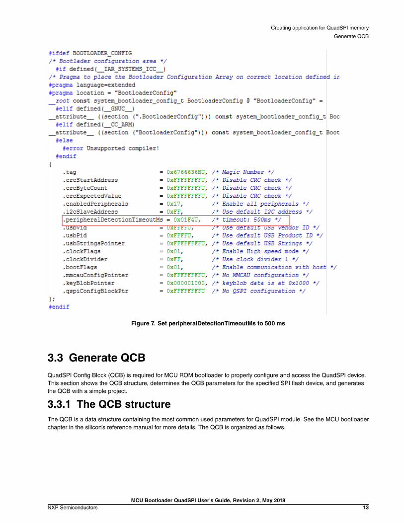
Figure 7. Set peripheralDetectionTimeoutMs to 500 ms
3.3 Generate QCBQuadSPI Config Block (QCB) is required for MCU ROM bootloader to properly configure and access the QuadSPI device.This section shows the QCB structure, determines the QCB parameters for the specified SPI flash device, and generatesthe QCB with a simple project.
3.3.1 The QCB structureThe QCB is a data structure containing the most common used parameters for QuadSPI module. See the MCU bootloaderchapter in the silicon’s reference manual for more details. The QCB is organized as follows.
Creating application for QuadSPI memory
Generate QCB
MCU Bootloader QuadSPI User's Guide, Revision 2, May 2018NXP Semiconductors 13

Table 2. QuadSPI configuration block
Offset Size (bytes) Configuration field Description
0x00 - 0x03 4 tag Magic number to verify whether QCB is valid.Must be set to ‘kqcf’.
[31:24] - ‘f’ (0x66)
[23:16] - ‘c’ (0x63)
[15: 8] - ‘q’(0x71)
[7: 0] - ‘k’(0x6B)
0x04 - 0x07 4 version Version number of QuadSPI config block.
[31:24] - name: must be ‘Q’(0x51)
[23:16] - major: must be 1
[15: 8] - minor: must be 1
[7: 0] - bugfix: must be 0
0x08 - 0x0b 4 lengthInBytes Size of QuadSPI config block, in terms ofbytes.
Must be 512.
0x0c - 0x0f 4 dqs_loopback Enable DQS loopback support:
0 DQS loopback is disabled.
1 DQS loopback is enabledd, the DQS loopbackmode is determined by subsequent'dqs_loopback_internal' field.
0x10 - 0x13 4 data_hold_time Serial flash data hold time. Valid value 0/1/2.See the QuadSPI Chapter for details.
0x14 - 0x1b 8 - Reserved.
0x1c - 0x1f 4 device_mode_config_en
Configure work mode enable for external flashdevices:
0 Disabled - ROM does not configure work modeof external flash devices.
1 Enabled - ROM configures work mode ofexternal flash devices based on "device_cmd"and LUT entries indicated by "write_cmd_ipcr".
0x20 - 0x23 4 device_cmd Command to configure work mode of externalflash devices. Effective only if"device_mode_config_en" is set to 1.
This command is device-specific.
Table continues on the next page...
Creating application for QuadSPI memory
Generate QCB
MCU Bootloader QuadSPI User's Guide, Revision 2, May 201814 NXP Semiconductors

Table 2. QuadSPI configuration block (continued)
Offset Size (bytes) Configuration field Description
0x24 - 0x27 4 write_cmd_ipcr IPCR pointed to LUT index for the commandsequence of configuring the device to workmode.
Value = index<<24
0x28 - 0x2b 4 word_addressable Word addressable:
0 Byte addressable serial flash mode.
1 Word addressable serial flash mode.
0x2c - 0x2f 4 cs_hold_time Serial flash CS hold time in terms of flash clockcycles.
0x30 - 0x33 4 cs_setup_time Serial flash CS setup time in terms of flashclock cycles.
0x34 - 0x37 4 sflash_A1_size Size of external flash connected to ports ofQSPI0A and QSPI0A_CS0, in terms of bytes.
0x38 - 0x3b 4 sflash_A2_size Size of external flash connected to ports ofQSPI0B and quadSPI0A_CS1, in terms ofbytes.
This field must be set to 0 if the serial flashdevices are not present.
0x3c - 0x3f 4 sflash_B1_size Size of external flash connected to ports ofQSPI0B and quadSPI0B_CS0, in terms ofbytes.
This field must be set to 0 if the serial flashdevices are not present.
0x40 - 0x43 4 sflash_B2_size Size of external flash connected to ports ofQSPI0B and quadSPI0B_CS1, in terms ofbytes.
This field must be set to 0 if the serial flashdevices are not present.
0x44 - 0x47 4 sclk_freq Frequency of QuadSPI serial clock:
0 Low frequency
1 Mid frequency
2 High frequency
See the MCU bootloader chapter in silicon’sreference manual for the definition of low-frequency, mid-frequency and high-frequency. InMK82F256, they are 24 MHz, 48 MHz, and 96MHz.
Table continues on the next page...
Creating application for QuadSPI memory
Generate QCB
MCU Bootloader QuadSPI User's Guide, Revision 2, May 2018NXP Semiconductors 15

Table 2. QuadSPI configuration block (continued)
Offset Size (bytes) Configuration field Description
0x48 - 0x4b 4 busy_bit_offset Busy bit offset in status register of Serial flash[31:16]:
0 - Busy flag in status register is 1 when flashdevices are busy.
1 - Busy flag in status register is 0 when flashdevices are busy.
[15:0]:
The offset of busy flag in status register, validrange 0-31.
0x4c - 0x4f 4 sflash_type Type of serial flash:
0 Single-pad
1 Dual-pad
2 Quad-pad
3 Octal-pad
0x50 - 0x53 4 sflash_port Port enablement for QuadSPI module:
0 Only pins for QSPI0A are enabled.
1 Pins for both QSPI0A and QSPI0B areenabled.
0x54 - 0x57 4 ddr_mode_enable Enable DDR mode:
0 DDR mode is disabled.
1 DDR mode is enabled.
0x58 - 0x5b 4 dqs_enable Enable DQS:
0 DQS is disabled.
1 DQS is enabled.
0x5c - 0x5f 4 parallel_mode_enable Enable Parallel Mode:
0 Parallel mode is disabled.
1 Parallel mode is enabled.
0x60 - 0x63 4 portA_cs1 Enable QuadSPI0A_CS1:
0 QuadSPI0A_CS1 is disabled.
1 QuadSPI0A_CS1 is enabled.
This field must be set to 1 if sflash_A2_size isnot equal to 0.
Table continues on the next page...
Creating application for QuadSPI memory
Generate QCB
MCU Bootloader QuadSPI User's Guide, Revision 2, May 201816 NXP Semiconductors

Table 2. QuadSPI configuration block (continued)
Offset Size (bytes) Configuration field Description
0x64 - 0x67 4 portB_cs1 Enable QuadSPI0B_CS1
0 QuadSPI0B_CS1 is disabled
1 QuadSPI0B_CS1 is enabled
This field must be set to 1 if sflash_B2_size isnot equal to 0.
0x68 - 0x6b 4 fsphs Full Speed Phase selection for SDRinstructions:
0 Select sampling at non-inverted clock.
1 Select sampling inverted clock.
0x6c - 0x6f 4 fsdly Full Speed Delay selection for SDRinstructions:
0 One clock cycle delay.
1 Two clock cycles delay.
0x70 - 0x73 4 ddrsmp DDR sampling point:
Valid range: 0 - 7.
0x74 - 0x173 256 look_up_table Look-up-table for sequences of instructions.
See the QuadSPI chapter in silicon’s referencemanual for more details.
0x174 - 0x177 4 column_address_space
Column Address Space:
The parameter defines the width of the columnaddress.
0x178 - 0x17b 4 config_cmd_en Enable additional configuration command:
0 Additional configuration command is notneeded.
1 Additional configuration command is needed.
0x17c - 0x18b 16 config_cmds IPCR arrays for each connected SPI flash.
"config_cmds[n]" provides IPCR value, namelyseq_id << 24.
All fields must be set to 0 if config_cmd_en is notset.
Table continues on the next page...
Creating application for QuadSPI memory
Generate QCB
MCU Bootloader QuadSPI User's Guide, Revision 2, May 2018NXP Semiconductors 17

Table 2. QuadSPI configuration block (continued)
Offset Size (bytes) Configuration field Description
0x18c - 0x19b 16 config_cmds_args Command arrays needed to be transferred toexternal SPI flash.
"config_cmds_args[n]" provides commands tobe written.
All fields must be set to 0 if config_cmd_en is notasserted.
0x19c - 0x19f 4 differential_clock_pin_enable
Enable differential flash clock pin:
0 Differential flash clock pin is disabled.
1 Differential flash clock pin is enabled.
0x1a0 - 0x1a3 4 flash_CK2_clock_pin_enable
Enable flash CK2 clock pin:
0 Flash CK2 clock pin is disabled.
1 Flash CK2 clock pin is enabled.
0x1a4 - 0x1a7 4 dqs_inverse_sel Select clock source for internal DQSgeneration:
0 Use 1x internal reference clock for DQSgeneration.
1 Use inverse 1x internal reference clock for theDQS generation.
0x1a8 - 0x1ab 4 dqs_latency_enable DQS Latency Enable:
0 DQS latency disabled.
1 DQS feature with latency included enabled.
0x1ac - 0x1af 4 dqs_loopback_internal DQS loop back from internal DQS signal orDQS Pad:
0 DQS loop back is sent to DQS pad first andthen looped back to QuadSPI.
1 DQS loop back from internal DQS signaldirectly.
0x1b0 - 0x1b3 4 dqs_phase_sel Select Phase Shift for internal DQSgeneration:
0 No Phase shift.
1 Select 45 degree phase shift.
2 Select 90 degree phase shift.
3 Select 135 degree phase shift.
0x1b4 - 0x1b7 4 dqs_fa_delay_chain_sel
Delay chain tap number selection forQuadSPI0A DQS:
Valid range: 0-63
Table continues on the next page...
Creating application for QuadSPI memory
Generate QCB
MCU Bootloader QuadSPI User's Guide, Revision 2, May 201818 NXP Semiconductors

Table 2. QuadSPI configuration block (continued)
Offset Size (bytes) Configuration field Description
0x1b8 - 0x1bb 4 dqs_fb_delay_chain_sel
Delay chain tap number selection forQuadSPI0B DQS:
Valid range: 0-63
0x1bc - 0x1c3 8 - Reserved.
0x1c4 - 0x1c7 4 page_size Page size of external flash.
Page size of all SPI flash devices must be thesame.
0x1c8 - 0x1cb 4 sector_size Sector size of exernal SPI in flash.
Sector size of all SPI flash devices must be thesame.
0x1cc - 0x1cf 4 timeout_milliseconds Timeout in terms of milliseconds:
0 Timeout check is disabled.
Other: QuadSPI Driver returns timeout if thetime that external SPI devices are busy lastsmore than this value.
0x1d0 - 0x1d3 4 ips_cmd_second_divider
Second driver for IPs command based onQSPI_MCR[SCLKCFG], the maximum value ofQSPI_MCR[SCLKCFG] depends on specificdevices.
0x1d4 - 0x1d7 4 need_multi_phase 0 Only one phase is needed to access externalflash devices.
1 Multiple phases are needed to erase/programexternal flash devices.
0x1d8 - 0x1db 4 is_spansion_hyperflash
0 External flash devices do not belong toCypress HyperFlash family.
1 External flash devices belong to CypressHyperFlash family.
0x1dc - 0x1df 4 pre_read_status_cmd_address_offset
Additional address for the PreReadStatuscommand.
Set this field to 0xFFFFFFFF if it is not required.
0x1e0 - 0x1e3 4 pre_unlock_cmd_address_offset
Additional address for PreWriteEnablecommand.
Set this field to 0xFFFFFFFF if it is not required.
0x1e4 - 0x1e7 4 unlock_cmd_address_offset
Additional address for WriteEnable command.
Set this field to 0xFFFFFFFFF if it is notrequired.
Table continues on the next page...
Creating application for QuadSPI memory
Generate QCB
MCU Bootloader QuadSPI User's Guide, Revision 2, May 2018NXP Semiconductors 19
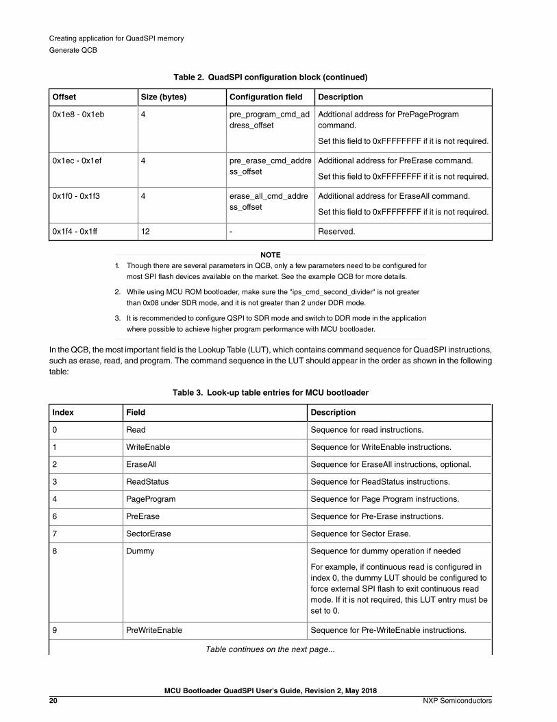
Table 2. QuadSPI configuration block (continued)
Offset Size (bytes) Configuration field Description
0x1e8 - 0x1eb 4 pre_program_cmd_address_offset
Addtional address for PrePageProgramcommand.
Set this field to 0xFFFFFFFF if it is not required.
0x1ec - 0x1ef 4 pre_erase_cmd_address_offset
Additional address for PreErase command.
Set this field to 0xFFFFFFFF if it is not required.
0x1f0 - 0x1f3 4 erase_all_cmd_address_offset
Additional address for EraseAll command.
Set this field to 0xFFFFFFFF if it is not required.
0x1f4 - 0x1ff 12 - Reserved.
1. Though there are several parameters in QCB, only a few parameters need to be configured for
most SPI flash devices available on the market. See the example QCB for more details.
2. While using MCU ROM bootloader, make sure the "ips_cmd_second_divider" is not greater
than 0x08 under SDR mode, and it is not greater than 2 under DDR mode.
3. It is recommended to configure QSPI to SDR mode and switch to DDR mode in the application
where possible to achieve higher program performance with MCU bootloader.
NOTE
In the QCB, the most important field is the Lookup Table (LUT), which contains command sequence for QuadSPI instructions,such as erase, read, and program. The command sequence in the LUT should appear in the order as shown in the followingtable:
Table 3. Look-up table entries for MCU bootloader
Index Field Description
0 Read Sequence for read instructions.
1 WriteEnable Sequence for WriteEnable instructions.
2 EraseAll Sequence for EraseAll instructions, optional.
3 ReadStatus Sequence for ReadStatus instructions.
4 PageProgram Sequence for Page Program instructions.
6 PreErase Sequence for Pre-Erase instructions.
7 SectorErase Sequence for Sector Erase.
8 Dummy Sequence for dummy operation if needed
For example, if continuous read is configured inindex 0, the dummy LUT should be configured toforce external SPI flash to exit continuous readmode. If it is not required, this LUT entry must beset to 0.
9 PreWriteEnable Sequence for Pre-WriteEnable instructions.
Table continues on the next page...
Creating application for QuadSPI memory
Generate QCB
MCU Bootloader QuadSPI User's Guide, Revision 2, May 201820 NXP Semiconductors

Table 3. Look-up table entries for MCU bootloader (continued)
Index Field Description
10 PrePageProgram Sequence for Pre-PageProgram instructions.
11 PreReadStatus Sequence for Pre-ReadStatus instructions.
5, 12, 13, 14, 15 Undefined All of these sequences are free to be used for otherpurposes. I.e., index 5 can be used for enablingQuad mode of SPI flash devices. For more details,see Section 3.3.2, "Example QCB forMX25U3235F device on TWR-K80F150M TowerSystem module".
For most types of SPI, flash devices are available in the market. Only index 0, 1, 3, 4, 7, and 8 are required. However, forother types of high-end SPI flash devices, such as Cypress HyperFlash, additional indexes listed above may be required.
3.3.2 Example QCB for MX25U3235F device on TWR-K80F150MTower System module
This section creates an example QCB data structure for TWR-K80F150M Tower System module. There are two MX25U3235FQuadSPI flash devices connected to QuadSPI0A and QuadSPI0B ports, respectively, on the board. The datasheet forMX25U3235F are available on the MXIC website, and the schematics for the TWR-K80F150M Tower System module isavailable on the NXP website.
The following are some attributes which are essential to create the QCB for the MX25U3235F flash device. The same (butnot limited to the following) information can be found in its data sheet as well:
Table 4. MX25U3235F features for QuadSPI configuration
Attribute Value/timing Description
Maximum supported frequency (4 I/O) 104 MHz (6 dummy cycles) -
Page size 256 bytes -
Sector size 4 KB/32 KB/64 KB 4 KB is selected in this guide.
Chip size 4 MB -
Busy/WriteInProgress bit in statusregister
Bit 0 Bit 0 in status registers is called busyflag.
1 means SPI flash device is busy.
0 means it is idle.
The value needs to be set to'busy_bit_offset' in QCB.
Table continues on the next page...
Creating application for QuadSPI memory
Generate QCB
MCU Bootloader QuadSPI User's Guide, Revision 2, May 2018NXP Semiconductors 21

Table 4. MX25U3235F features for QuadSPI configuration (continued)
Attribute Value/timing Description
Enable Quad mode Write status register, bit6 must be set to1 in order to enable Quad mode.
Following the QuadSPI chapter, thecommand sequence for this operationis:
1. CMD: 01, single pad
2. Write: length=1, single pad
The data to be written is 0x40, and isconfigured to 'device_cmd' in QCB.
Write Enable This is required before issuing any write/erase operations to SPI flash devices.
The command sequence for thisoperation is:
1. CMD: 0x06, single pad
Sector Erase Each sector must be erased beforedoing any program operation.
The command sequence for thisoperation is:
1. CMD: 0x20, single pad
2. ADDR: 0x18 (24-bit address), singlepad
Chip Erase This command can be used to erase theentire content on SPI flash device.
The command sequence for thisoperation is:
1. CMD: 0x60, single pad
Table continues on the next page...
Creating application for QuadSPI memory
Generate QCB
MCU Bootloader QuadSPI User's Guide, Revision 2, May 201822 NXP Semiconductors

Table 4. MX25U3235F features for QuadSPI configuration (continued)
Attribute Value/timing Description
4 x I/O Page program This command is used to program thedesired data to SPI flash device. Here,we use 4 x I/O page program commandin order to improve the programperformance.
The command sequences for thisoperation are:
1. CMD: 0x38, single pad
2. ADDR: 0x18 (24 bit address) quadpads
3. WRITE: 0x40 (ignore this value)quad pads
4 I/O Read This command is used to read data fromSPI flash device. Here, we use 4 x I/ORead in order to improve readperformance.
The command sequence for thisoperation is:
1. CMD: 0xEB, single pad
2. ADDR: 0x18 (24 bit address) quadpads
3. DUMMY: 0x06 (6 cycles) quad pads
4. READ: 0x80 (128 byte at one pass)quad pads
5. JUMP_ON_CS: 0 (single pad)
Read Status This command is used to check if theSPI flash device is busy after havingissued a program/erase command to it.
The command sequence for thisoperation is:
1. CMD: 0x05, single pad
2. READ: 1 (byte) single pad
The information needed for QCB creation for the TWR-K80F150M Tower System module is summarized in Table 4. The“Programmable Sequence Engine” and "Example Sequences" sections within the QuadSPI chapter of the MK80F256Reference Manual can be referenced to create customized QCBs. The “Description” column in Table 4 also provides the LUTinstructions for each command.
Based on the above summary, the ‘qspi_config_block_generator’ project is provided with the package as an example alongwith this user's guide. The example project can be used as a basis to generate customized QCBs.
Creating application for QuadSPI memory
Generate QCB
MCU Bootloader QuadSPI User's Guide, Revision 2, May 2018NXP Semiconductors 23

3.3.3 Generate the QCB with a simple example projectThe project can be found in the package at location <sdk_package>/middleware/mcu-boot/apps/QCBGenerator/build.Currently, two projects are provided to build from toolchains Microsoft Visual Studio 2013 and codeblocks. Launch MicrosoftVisual Studio example project available in the Visual Studio folder. Edit the file qspi_config_block_generator.c to configureqspi_config_block in the main function.
There are two examples using different ways to enable Quad mode. The first one enables Quad mode using the device modeconfig feature, while the second one enables Quad mode using the config cmd feature. See the below examples for moredetails.
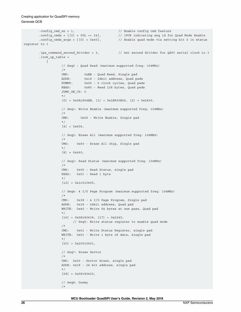
1. QCB using the device mode config feature:
const qspi_config_t qspi_config_block = { .tag = kQspiConfigTag, // Fixed value, do not change. .version = { .version = kQspiVersionTag }, // Fixed value, do not change. .lengthInBytes = 512, // Fixed value, do not change. .sflash_A1_size = 0x400000, // 4MB - MX25U3235F connected to QSPI0A .sflash_B1_size = 0x400000, // 4MB - MX25U3235F connected to QSPI0B // In K80 ROM bootloader, QSPI serial clock frequency is 96MHz .sclk_freq = kQspiSerialClockFreq_High, // High frequency, 96MHz / 1 = 96MHz .sflash_type = kQspiFlashPad_Quad, // SPI Flash devices work under quad-pad mode .sflash_port = kQspiPort_EnableBothPorts, // Both QSPI0A and QSPI0B are enabled. .busy_bit_offset = 0, // Busy offset is 0 .ddr_mode_enable = 0, // disable DDR mode .dqs_enable = 0, // Disable DQS feature .parallel_mode_enable = 0, // QuadSPI module work under serial mode .pagesize = 256, // Page Size: 256 bytes .sectorsize = 0x1000, // Sector Size: 4KB .device_mode_config_en = 1, // configure quad mode for SPI flash device .device_cmd = 0x40, // Enable quad mode .write_cmd_ipcr = 0x05000000U, // IPCR indicating enable seqid (5<<24), see QCB structure // Set second divider for QSPI serial clock to 3 if K80 ROM Bootloader cannot program // SPI flash at 96 MHz, in this configuration, the program speed is 96MHz/4 = 24MHz .ips_command_second_divider = 3, .look_up_table = { // Seq0: Quad Read (maximum supported freq: 104MHz) /* CMD: 0xEB - Quad Read, Single pad ADDR: 0x18 - 24bit address, Quad pads DUMMY: 0x06 - 6 clock cycles, Quad pads READ: 0x80 - Read 128 bytes, Quad pads JUMP_ON_CS: 0 */ [0] = 0x0A1804EB, [1] = 0x1E800E06, [2] = 0x2400, // Seq1: Write Enable (maximum supported freq: 104MHz) /* CMD: 0x06 - Write Enable, Single pad */ [4] = 0x406, // Seq2: Erase all (maximum supported freq: 104MHz) /* CMD: 0x60 - Erase All chip, Single pad */
Creating application for QuadSPI memory
Generate QCB
MCU Bootloader QuadSPI User's Guide, Revision 2, May 201824 NXP Semiconductors

[8] = 0x460, // Seq3: Read Status (maximum supported freq: 104MHz) /* CMD: 0x05 - Read Status, single pad READ: 0x01 - Read 1 byte */ [12] = 0x1c010405, // Seq4: 4 I/O Page Program (maximum supported freq: 104MHz) /* CMD: 0x38 - 4 I/O Page Program, Single pad ADDR: 0x18 - 24bit address, Quad pad WRITE: 0x40 - Write 64 bytes at one pass, Quad pad, (Ignore the 64, because it will be overwritten by page size) */ [16] = 0x0A180438, [17] = 0x2240, // Seq5: Write status register to enable quad mode /* CMD: 0x01 - Write Status Register, single pad WRITE: 0x01 - Write 1 byte of data, single pad */ [20] = 0x20010401, // Seq7: Erase Sector /* CMD: 0x20 - Sector Erase, single pad ADDR: 0x18 - 24 bit address, single pad */ [28] = 0x08180420, // Seq8: Dummy /* CMD: 0 - Dummy command, used to force SPI flash to exit continuous read mode. Unnecessary here because the continuous read mode isn't enabled. */ [32] = 0, },};
2. QCB using the config cmd feature:
const qspi_config_t qspi_config_block = { .tag = kQspiConfigTag, // Fixed value, do not change .version = {.version = kQspiVersionTag}, // Fixed value, do not change .lengthInBytes = 512, // Fixed value, do not change .sflash_A1_size = 0x400000, // 4MB .sclk_freq = kQspiSerialClockFreq_High, // High frequency, in K82-256, it means 96MHz/1 = 96MHz .sflash_type = kQspiFlashPad_Quad, // SPI Flash devices work under quad-pad mode .sflash_port = kQspiPort_EnableBothPorts, // Both QSPI0A and QSPI0B are enabled. .busy_bit_offset = 0, // Busy offset is 0 .ddr_mode_enable = 0, // disable DDR mode .dqs_enable = 0, // Disable DQS feature .parallel_mode_enable = 0, // QuadSPI module work under serial mode .pagesize = 256, // Page Size : 256 bytes .sectorsize = 0x1000, // Sector Size: 4KB
Creating application for QuadSPI memory
Generate QCB
MCU Bootloader QuadSPI User's Guide, Revision 2, May 2018NXP Semiconductors 25
.config_cmd_en = 1, // Enable config cmd feature .config_cmds = {[0] = 5UL << 24}, // IPCR indicating seq id for Quad Mode Enable .config_cmds_args = {[0] = 0x40}, // Enable quad mode via setting bit 6 in status register to 1
.ips_command_second_divider = 3, // Set second divider for QSPI serial clock to 3 .look_up_table = { // Seq0 : Quad Read (maximum supported freq: 104MHz) /* CMD: 0xEB - Quad Read, Single pad ADDR: 0x18 - 24bit address, Quad pads DUMMY: 0x06 - 6 clock cycles, Quad pads READ: 0x80 - Read 128 bytes, Quad pads JUMP_ON_CS: 0 */ [0] = 0x0A1804EB, [1] = 0x1E800E06, [2] = 0x2400,
// Seq1: Write Enable (maximum supported freq: 104MHz) /* CMD: 0x06 - Write Enable, Single pad */ [4] = 0x406,
// Seq2: Erase All (maximum supported freq: 104MHz) /* CMD: 0x60 - Erase All chip, Single pad */ [8] = 0x460,
// Seq3: Read Status (maximum supported freq: 104MHz) /* CMD: 0x05 - Read Status, single pad READ: 0x01 - Read 1 byte */ [12] = 0x1c010405,
// Seq4: 4 I/O Page Program (maximum supported freq: 104MHz) /* CMD: 0x38 - 4 I/O Page Program, Single pad ADDR: 0x18 - 24bit address, Quad pad WRITE: 0x40 - Write 64 bytes at one pass, Quad pad */ [16] = 0x0A180438, [17] = 0x2240, // Seq5: Write status register to enable quad mode /* CMD: 0x01 - Write Status Register, single pad WRITE: 0x01 - Write 1 byte of data, single pad */ [20] = 0x20010401,
// Seq7: Erase Sector /* CMD: 0x20 - Sector Erase, single pad ADDR: 0x18 - 24 bit address, single pad */ [28] = 0x08180420,
// Seq8: Dummy /*
Creating application for QuadSPI memory
Generate QCB
MCU Bootloader QuadSPI User's Guide, Revision 2, May 201826 NXP Semiconductors
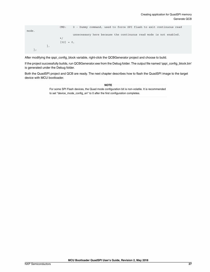
CMD: 0 - Dummy command, used to force SPI flash to exit continuous read mode. unnecessary here because the continuous read mode is not enabled. */ [32] = 0, }, };
After modifying the qspi_config_block variable, right-click the QCBGenerator project and choose to build.
If the project successfully builds, run QCBGenerator.exe from the Debug folder. The output file named 'qspi_config_block.bin'is generated under the Debug folder.
Both the QuadSPI project and QCB are ready. The next chapter describes how to flash the QuadSPI image to the targetdevice with MCU bootloader.
For some SPI Flash devices, the Quad mode configuration bit is non-volatile. It is recommended
to set "device_mode_config_en" to 0 after the first configuration completes.
NOTE
Creating application for QuadSPI memory
Generate QCB
MCU Bootloader QuadSPI User's Guide, Revision 2, May 2018NXP Semiconductors 27
Chapter 4Configure QuadSPI with MCU bootloader
QuadSPI can be configured using the MCU bootloader by:
1. Configure QuadSPI at runtime.
2. Configure QuadSPI at start-up.
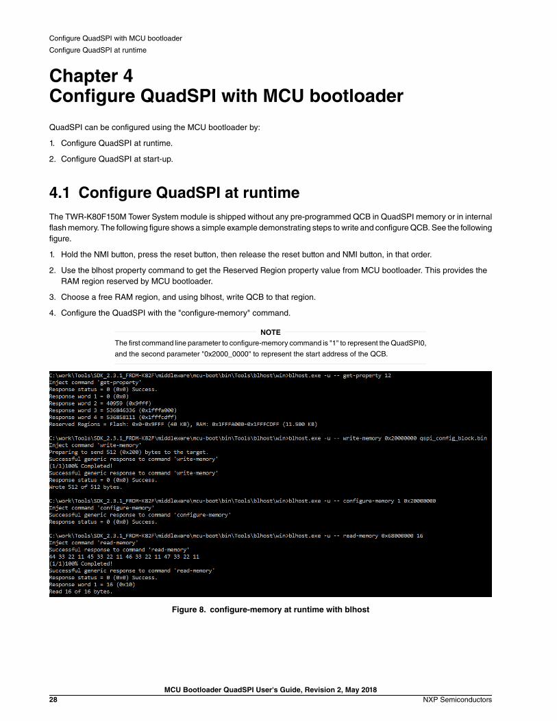
4.1 Configure QuadSPI at runtimeThe TWR-K80F150M Tower System module is shipped without any pre-programmed QCB in QuadSPI memory or in internalflash memory. The following figure shows a simple example demonstrating steps to write and configure QCB. See the followingfigure.
1. Hold the NMI button, press the reset button, then release the reset button and NMI button, in that order.
2. Use the blhost property command to get the Reserved Region property value from MCU bootloader. This provides theRAM region reserved by MCU bootloader.
3. Choose a free RAM region, and using blhost, write QCB to that region.
4. Configure the QuadSPI with the "configure-memory" command.
The first command line parameter to configure-memory command is "1" to represent the QuadSPI0,
and the second parameter "0x2000_0000" to represent the start address of the QCB.
NOTE
Figure 8. configure-memory at runtime with blhost
Configure QuadSPI with MCU bootloader
Configure QuadSPI at runtime
MCU Bootloader QuadSPI User's Guide, Revision 2, May 201828 NXP Semiconductors

4.2 Configure QuadSPI at start-upThe previous sections show how to configure QCB when there is no QCB pre-programmed on the device. For subsequentboots, it makes sense to save the QCB to non-volatile memory, such as internal flash pointed by the BCA member field,'qspiConfigBlockPtr', or at the start offset of QuadSPI memory. Next time the device boots from the ROM, the MCU bootloaderin ROM detects the presence of the QCB and configure the QuadSPI automatically at start-up. The following steps are therecommended procedure based on the previous section. To program QCB at the start address of QuadSPI memory, see thefollowing figure for the blhost command sequence.
1. Erase the first sector in QuadSPI memory before programming the QCB.
2. Write the QCB to the start of QuadSPI memory.
3. Erase the flash config area.
4. Program the FOPT with the desired value. Make sure FOPT[7:6] (0x40D address in internal flash) is set to 0b10 to defaultto boot from MCU bootloader in ROM.
5. Reset the target device and use the "read-memory command" to check and ensure if QuadSPI is configured successfullyat start-up, as shown in the following figure.
When all of the above operations are completed, the QuadSPI is configured at start-up.
So far, we understand the basic steps of creating QCB and configuring QuadSPI using the MCU bootloader. The next sectionsdescribe how to program the QuadSPI image.
Configure QuadSPI with MCU bootloader
Configure QuadSPI at start-up
MCU Bootloader QuadSPI User's Guide, Revision 2, May 2018NXP Semiconductors 29
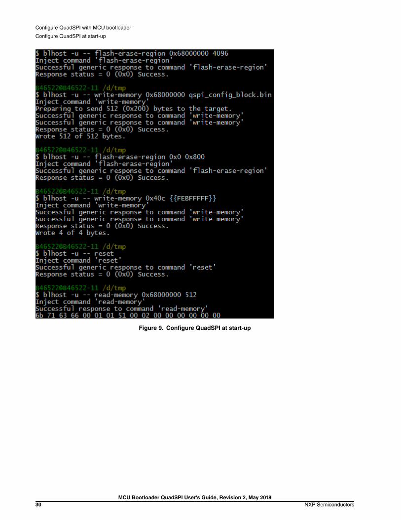
Figure 9. Configure QuadSPI at start-up
Configure QuadSPI with MCU bootloader
Configure QuadSPI at start-up
MCU Bootloader QuadSPI User's Guide, Revision 2, May 201830 NXP Semiconductors
Chapter 5Flash QuadSPI image via SB file
Generally, the QuadSPI image contains separate segments. For example, the vector table and the flash config area are inthe internal flash and the executable code is located in the QuadSPI memory. Additionally, the corresponding regions mustbe erased before programming. It is inconvenient to use separate commands to finish this task. Here, we introduce the SBfiles and the “receive-sb-file” command to simplify the programming procedure.
5.1 Brief introduction of SB fileThe MCU bootloader supports loading of the SB files. The SB file is a NXP-defined boot file format designed to ease theboot process. The file is generated using the NXP elftosb tool. The format supports loading of elf or srec files in a controlledmanner, using boot commands such as load, jump, fill, erase, and so on. The boot commands are prescribed in the inputcommand file (boot descriptor .bd) to the elftosb tool. The format supports encryption of the boot image using AES-128 inputkey.
elftosb and SB file formats are described in greater detail in the accompanying documentation in the package.
In this user's guide, the typical use case is provided to demonstrate the usage of elftosb host tool and how to download theSB file with MCU bootloader.
5.2 Generate SB file for QuadSPI imageThis section describes the generation of the SB file. The output led-demo srec file is used to generate the SB file (for KEIL,a similar approach can be followed).
• Open the led_demo_qspi project using the IAR EWARM toolchain. Using the project options dialog, select the "linker" andmake sure the extension of the output file is ".out".
• Select the "Output Converter" and change the output format to "Motorola" for outputting the .srec format image. See thefollowing figure.
Flash QuadSPI image via SB file
Brief introduction of SB file
MCU Bootloader QuadSPI User's Guide, Revision 2, May 2018NXP Semiconductors 31

Figure 10. Generate led_demo_qspi.srec with EWARM
• Build either the Debug or the Release configuration of the project. When the build is completed, the led_demo_QSPI.srecfile should be available in the output/Debug or output/Release folders.
The next step is to generate the SB file using a command-line host tool, elftosb. The boot descriptor file, qspi_image.bd, ispassed as the input to the elftosb tool on the command line. The following figure shows the BD file content, the "Sources"section provides the path to the input srec and QCB files and "Section (0)" shows the flow of the boot commands.
After creating the BD file shown in the following figure, copy the "qspi_config_block.bin", elftosb.exe, "led_demo_QSPI.srec",and BD files into the same directory. Then open the window with the command prompt and invoke the elftosb as “elftosb –V–c qspi_image.bd –o image.sb”. The elftosb processes the qspi_image.bd file and generates the image.sb file. The elftosbalso outputs the commands list, as shown in Figure 12. Notice that the list corresponds to the BD file Section(0) statements.
Flash QuadSPI image via SB file
Generate SB file for QuadSPI image
MCU Bootloader QuadSPI User's Guide, Revision 2, May 201832 NXP Semiconductors
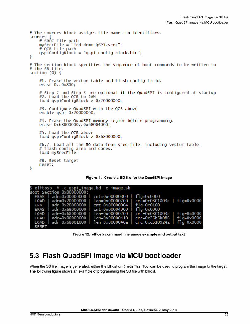
Figure 11. Create a BD file for the QuadSPI image
Figure 12. elftosb command line usage example and output text
5.3 Flash QuadSPI image via MCU bootloaderWhen the SB file image is generated, either the blhost or KinetisFlashTool can be used to program the image to the target.The following figure shows an example of programming the SB file with blhost.
Flash QuadSPI image via SB file
Flash QuadSPI image via MCU bootloader
MCU Bootloader QuadSPI User's Guide, Revision 2, May 2018NXP Semiconductors 33
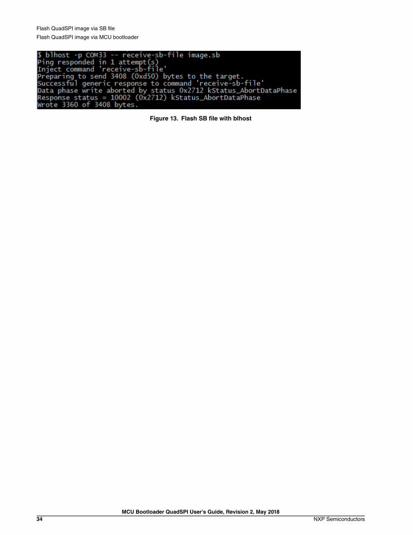
Figure 13. Flash SB file with blhost
Flash QuadSPI image via SB file
Flash QuadSPI image via MCU bootloader
MCU Bootloader QuadSPI User's Guide, Revision 2, May 201834 NXP Semiconductors

Chapter 6Advanced Usage: Encrypted QuadSPI image
The SB file generated in Section 5.2 is in plaintext form and not encrypted. This section focuses on several aspects ofencrypted boot with MCU bootloader.
To use the encrypted boot feature, user must have basic knowledge of the SB key, KeyBlob Block, and KeyBlob EncryptionKey (KEK), SB Key, AES-128 CTR, AES-128 CBC-MAC, and so on. See the MCU bootloader chapter in the silicon's referencemanual for a detailed description. The following is a brief introduction to these terms:
• The KeyBlob Block is a data structure that contains up to four groups of KeyBlob entries. Each entry consists of the startaddress, length, decryption key, and counter of an encrypted QuadSPI memory region.
• The KeyBlob Block itself is encrypted by another AES key, called Key encryption key (KEK). KEK needs to be pre-programmed in flash's IFR region. In MK82F256, the Flash IFR index for KEK is from index 0x20 to 0x23. With the KeyBlob and KEK, sections belonging to encrypted QuadSPI memory region (QuadSPI image data) can be encrypted usingelftosb tools. The generated SB file has encrypted image data for the encrypted QuadSPI memory region.
• For devices with flash security enabled, only encrypted SB file images are allowed to be provisioned. MCU bootloaderdecrypts the encrypted SB image as it receives from the host using a separate SB key. The SB key is an AES-128 key pre-programmed into flash's IFR region at word offsets 0x30 to 0x33. The elftosb tool allows generation of encrypted SB fileimage using the SB key.
In general, the QuadSPI image is encrypted using the parameters in the KeyBlob with AES-128 CTR mode, the KeyBlobBlock itself encrypted with KEK, and the SB file is encrypted via SB key with AES-128 CBC-MAC. The following figure showsan SB file containing plaintext QuadSPI image data. The vector table and other regions are in plaintext.
Based on the application type, the user can choose to have plaintext or encrypted QuadSPI image or encrypted SB file imagesolution.
Figure 14. Plaintext SB file with Plaintext QuadSPI image
Advanced Usage: Encrypted QuadSPI image
MCU Bootloader QuadSPI User's Guide, Revision 2, May 2018NXP Semiconductors 35

Figure 15. Plaintext SB file with Encrypted QuadSPI image
The following figure provides an encrypted SB file containing an encrypted QuadSPI image. The entire content of the SB fileis obfuscated.
Figure 16. Encrypted SB file with Encrypted QuadSPI image
The rest of the sections in this chapter provide step-by-step instructions on programming keys, generating encrypted QuadSPIimage data in the SB file, and encrypting the entire SB file image with the SB key.
6.1 Generate an SB file with KEK and SB KEYHere is an example of generating an SB file with just the KEK and SB KEY. The generated SB file can be provisioned usingMCU bootloader to program the keys into IFR region of the device.
The SB KEY is a 16 byte array. For example:
uint8_t sbKey[16] = {0x00, 0x11, 0x22, 0x33, 0x44, 0x55, 0x66, 0x77, 0x88, 0x99, 0xaa, 0xbb, 0xcc, 0xdd, 0xee, 0xff}.
Advanced Usage: Encrypted QuadSPI image
Generate an SB file with KEK and SB KEY
MCU Bootloader QuadSPI User's Guide, Revision 2, May 201836 NXP Semiconductors

The KEK is also a 16 byte array. For example:
uint8_t kek[16] = {0x00, 0x01, 0x02, 0x03, 0x04, 0x05, 0x06, 0x07, 0x08, 0x09, 0x0a, 0x0b, 0x0c, 0x0d, 0x0e, 0x0f}.
Pay attention to the correct order of the data to be programmed to Flash IFR, because each IFR field needs to be programmedwith 32-bit little-endian data. See the example BD file content provided in the following figure to understand how to specifythe SB key and KEK to generate SB file image to program the keys.
To generate SB file, a specified BD file needs to be generated first, assuming the BD file is called "program_keys.bd".
Figure 17. Specified BD file for SB key and KEK
Using elftosb, the desired SB file is generated. The elftosb command line and output is shown in the following figure.
Figure 18. Generate program_keys.sb
Either blhost or KinetisFlashTool can be used to flash the SB file to the target device.
6.2 Generate an SB file with encrypted QuadSPI imageAfter the previous operation, another SB file (which contains the encrypted QuadSPI image) is still needed. Similar to howthe SB file was generated in the previous section, the BD file is needed to describe all the operations in this SB file. Besides
Advanced Usage: Encrypted QuadSPI image
Generate an SB file with encrypted QuadSPI image
MCU Bootloader QuadSPI User's Guide, Revision 2, May 2018NXP Semiconductors 37
the operations listed in Chapter 4, it also contains the Key Blob Block, encrypted QuadSPI image, and Key Blob encryptionwrapper.
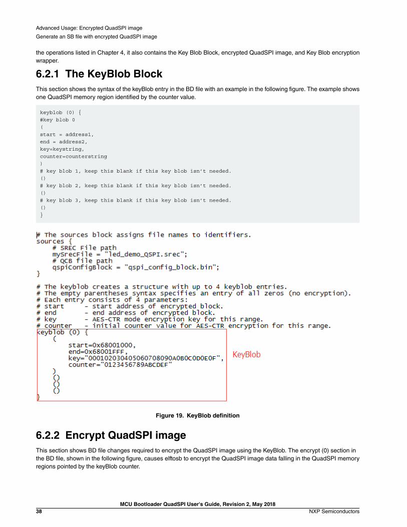
6.2.1 The KeyBlob BlockThis section shows the syntax of the keyBlob entry in the BD file with an example in the following figure. The example showsone QuadSPI memory region identified by the counter value.
keyblob (0) {#key blob 0(start = address1, end = address2, key=keystring, counter=counterstring)# key blob 1, keep this blank if this key blob isn’t needed. ()# key blob 2, keep this blank if this key blob isn’t needed.()# key blob 3, keep this blank if this key blob isn’t needed.()}
Figure 19. KeyBlob definition
6.2.2 Encrypt QuadSPI imageThis section shows BD file changes required to encrypt the QuadSPI image using the KeyBlob. The encrypt (0) section inthe BD file, shown in the following figure, causes elftosb to encrypt the QuadSPI image data falling in the QuadSPI memoryregions pointed by the keyBlob counter.
Advanced Usage: Encrypted QuadSPI image
Generate an SB file with encrypted QuadSPI image
MCU Bootloader QuadSPI User's Guide, Revision 2, May 201838 NXP Semiconductors

The keyBlob itself is encrypted with the KEK. The keywrap (0) section in the BD file causes elftosb to wrap the keyBlob usingthe KEK specified in the load command of keywrap section.
The syntax for the keywrap section of BD file is as follows:
keywrap (0) { load {{KEK hex string}} > destination of encrypted key blob block; }
The memory address 0x1000 in the example shown in the following figure is where the wrapped keyBlob is loaded duringprovisioning of SB file to the target device using MCU bootloader.
Figure 20. Encrypt QuadSPI image and KeyBlob
6.2.3 Encrypting SB file with the SB keyTo encrypt the SB file with the elftosb, a file containing the SB key must be created, as shown in the following figure.
Advanced Usage: Encrypted QuadSPI image
Generate an SB file with encrypted QuadSPI image
MCU Bootloader QuadSPI User's Guide, Revision 2, May 2018NXP Semiconductors 39

Figure 21. Create key.txt containing SB key
The following figure shows the generation of the encrypted SB file using the BD file drafted in the previous sections. The SBkey is passed on the command line to the elftosb using the -k option.
Figure 22. Generate encrypted SB file with encrypted QuadSPI image
The output image.sb file can be programmed to the target device using the blhost or KinetisFlashTool, as shown in the earlierexamples. Based on the example BD file, the image.sb file has the wrapped keyBlob, the keyBlob encrypted QuadSPI imagedata, and the entire content of the SB file encrypted with the SB key.
Advanced Usage: Encrypted QuadSPI image
Generate an SB file with encrypted QuadSPI image
MCU Bootloader QuadSPI User's Guide, Revision 2, May 201840 NXP Semiconductors

Chapter 7Change QuadSPI clock in QuadSPI image
When using MCU bootloader, if the target is booted from the QuadSPI image, both the QuadSPI serial clock and core clockare from MCGFLL. MCG is under FEE mode, using the IRC48M as the clock source. In some cases, this may not meet thesystem’s accuracy and performance requirement. The MCG mode needs to be switched from FEE to PEE, with an externalOSC as clock source. Be aware that this operation has great impact on the QuadSPI serial clock, so avoid running the clockswitch function on the QuadSPI image directly. A relatively safer way to avoid this is to either copy this function to SRAM, orplace this function in internal flash.
This chapter provides an example for how to create a clock switch function running on RAM.
7.1 Create a RAM function via IAR EWARMIn order to create a RAM function with IAR EWARM, two sections need to be defined. The first is “ramfunc_section_init”, whichis used to store the data of a RAM function, and a “ramfunc_section”, which is the actual execution section of the RAM function.The following code snippets provide an example of how to define and place code to these sections.
Figure 23. Declare ram function section in EWARM project
After the previous operation, we still need to define another function. For example, copy_to_ram() to copy the RAM funccodes from QuadSPI memory to RAM. The following figure provides an example.
Figure 24. Implement copy_to_ram() function in EWARM project
Finally, change the linker file in order to let the linker know a RAM function section has been defined. The location to placethis section, and the section, need to be copied to RAM manually.
Change QuadSPI clock in QuadSPI image
Create a RAM function via IAR EWARM
MCU Bootloader QuadSPI User's Guide, Revision 2, May 2018NXP Semiconductors 41

Figure 25. Linker file changes for ram function in EWARM project
A complete project for this example can be found in <sdk_package>/boards/<board>/bootloader_examples/demo_apps.
7.2 Create a RAM function via Keil MDKKeil also supports the creation of a RAM function, using a similar method as described for IAR EWARM. To create a RAMfunction via KEIL, declare a section. In this example, "ramfunc_section" has been declared. See the following figure.
Figure 26. Declare RAM function in MDK project
A copy_to_ram function is still necessary to copy the data from ROM to an actual execution address. See the following figure.
Figure 27. Implement copy_to_ram() function in MDK project
To let the linker know a RAM function has been defined, add some information to the linker file. For example:
Change QuadSPI clock in QuadSPI image
Create a RAM function via Keil MDK
MCU Bootloader QuadSPI User's Guide, Revision 2, May 201842 NXP Semiconductors

Figure 28. Linker file changes for RAM function in MDK project
A complete project for this example can be found in the <sdk_package>/boards/<board>/bootloader_examples/demo_apps.
7.3 Create a RAM function with MCUXpresso IDEThis section shows the steps required for the MCUXpresso IDE to create the RAM function.
First, declare a section to place the RAM function codes to. In this example, a section called “ramfunc_section” is declaredas follows:
Figure 29. Declare a RAM function in MCUXpresso IDE
Then, implement the copy_to_ram() function in the MCUXpresso IDE project. An example is shown in the following figure:
Change QuadSPI clock in QuadSPI image
Create a RAM function with MCUXpresso IDE
MCU Bootloader QuadSPI User's Guide, Revision 2, May 2018NXP Semiconductors 43

Figure 30. Implement copy_to_ram() function in MCUXpresso IDE project
Finally, the linker file must be updated to let the MCUXpresso IDE realize that the RAM function is defined, and must beplaced somewhere. The following figure demonstrates the changes for the RAM function in the linker file. A complete projectfor this example can be found in the <sdk_package>/boards/<board>/bootloader_examples/demo_apps folder.
Figure 31. Linker file changes for RAM function in MCUXpresso IDE
Change QuadSPI clock in QuadSPI image
Create a RAM function with MCUXpresso IDE
MCU Bootloader QuadSPI User's Guide, Revision 2, May 201844 NXP Semiconductors

7.4 Ensure no timing issue after clock changeAfter performing the changes listed in the previous section, the clock switch function can be implemented. Note that the clockswitch function must not violate the timing requirements for the QuadSPI module and the external SPI flash device. Forexample, if the external SPI flash is working in the SDR mode and you plan to switch the QuadSPI clock source to PLL 120MHz, it is required to set the QuadSPI_MCR [SCLKCFG] to at least 1 (which means that the QuadSPI serial clock frequencyis 120 MHz/2 = 60 MHz), because the maximum supported clock for the SDR mode is 100 MHz. See the clock_change()function in the example for more details.
Change QuadSPI clock in QuadSPI image
Ensure no timing issue after clock change
MCU Bootloader QuadSPI User's Guide, Revision 2, May 2018NXP Semiconductors 45

Chapter 8Application running on QuadSPI alias area
For reasons such as performance improvements, the application should be addressed to run from QuadSPI alias area(0x0400_0000 to 0x07FF_FFFF on MK82F256) instead of physical addresses. MCU ROM bootloader does not supportdownloading the application running on the alias area directly. However, a workaround solution is described in this sectionto allow application to run from the alias region. Here we use the led_demo demonstrated before as an example and showhow to download and run such application from the alias memory region.
This section is only applicable to MCU ROM Bootloader in K80, K81, and K82.
NOTE
8.1 Create an application to run on QuadSPI Alias AreaUsing the led_demo_QSPI as a starting point, modify the linker file using the IAR project as an example. The following figureshows the changes to the address symbols in the linker file to allocate the sections to the QuadSPI alias memory.
Figure 32. Linker file changes for QuadSPI Alias image in IAR project
Next, remove the BOOTLOADER_CONFIG macro from the IAR project, because the BCA is placed in the internal flashmemory. In this example, the application is placed in the QuadSPI alias memory. See the following figure for details.
Application running on QuadSPI alias area
Create an application to run on QuadSPI Alias Area
MCU Bootloader QuadSPI User's Guide, Revision 2, May 201846 NXP Semiconductors

Figure 33. Remove BOOTLOADER_CONFIG macro from IAR project
Finally, change the "Output Converter" option, and let the IAR generate a binary file. See the following figure.
Application running on QuadSPI alias area
Create an application to run on QuadSPI Alias Area
MCU Bootloader QuadSPI User's Guide, Revision 2, May 2018NXP Semiconductors 47

Figure 34. Let IAR output binary file
8.2 Create a simple boot applicationAs previously mentioned, MCU boootloader does not support boot from QuadSPI alias memory directly, and as such thehost tool should command MCU bootloader to write the led_demo_QSPI application image to the physical address ofQuadSPI memory starting with 0x6800_0000 address range. The workaround to make the QuadSPI application run out ofalias memory is to create a simple boot application that, when invoked at boot, causes the PC to jump to the alias addresswhere led_demo_QSPI application is linked. The boot application functionality includes:
• Change the VTOR to the actual base address of the vector table in the led_demo_QuadSPI application.
• Change the stack pointed to the actual address pointed to in the start of the vector table for the led_demo_QuadSPIapplication.
• Jump to the led_demo_QuadSPI application.
In addition, the BCA and keyBlob also need to be included in the boot application. The example boot application is providedalong with the led_demo_QuadSPI in <sdk_package>/boards/<board>/bootloader_examples/demo_apps. The followingsteps demonstrate how to generate the project for the boot application:
First, use the led_demo_PFLASH as a starting point, and replace the main() function with the code snippet from the followingfigure.
Application running on QuadSPI alias area
Create a simple boot application
MCU Bootloader QuadSPI User's Guide, Revision 2, May 201848 NXP Semiconductors

Figure 35. Jump to application running on QuadSPI Alias Area
Next, change the startup_MK82F25616.s file. Ensure that FOPT [7:6] (loaded from address 0x40D) is set to 0b10. See thefollowing figure.
Figure 36. Change FOPT to 0xBD
Enable BCA in the boot project by defining BOOTLOADER_CONFIG macro. See the following figure.
Application running on QuadSPI alias area
Create a simple boot application
MCU Bootloader QuadSPI User's Guide, Revision 2, May 2018NXP Semiconductors 49

Figure 37. Change Enable BCA in IAR project
Change the BCA fields as needed. For example, if 'peripheralDetectionTimeoutMs' needs to be changed to 500 and the'keyBlobPointer' to 0x1000. The example BCA structure is shown in the following figure.
Application running on QuadSPI alias area
Create a simple boot application
MCU Bootloader QuadSPI User's Guide, Revision 2, May 201850 NXP Semiconductors

Figure 38. Update BCA
Finally, change the "Output Converter" option, and let the IAR output SREC file.
8.3 Downloading application running on QuadSPI aliasmemory with SB file
Assume that the application running on QuadSPI alias memory is called “led_demo_qspi_alias.bin”, the boot application iscalled “boot_to_qspi_alias_memory.srec”, and the QCB is called “qspi_config_block.bin”. An example BD file to generate therequired SB file is shown in the following figure. Note that only one SB file is needed to load both boot application"boot_to_qspi_alias_memory.srec" and led_demo_QuadSPI_alias.bin.
Figure 39. QuadSPI configurations flow in MCU bootloader
Application running on QuadSPI alias area
Downloading application running on QuadSPI alias memory with SB file
MCU Bootloader QuadSPI User's Guide, Revision 2, May 2018NXP Semiconductors 51
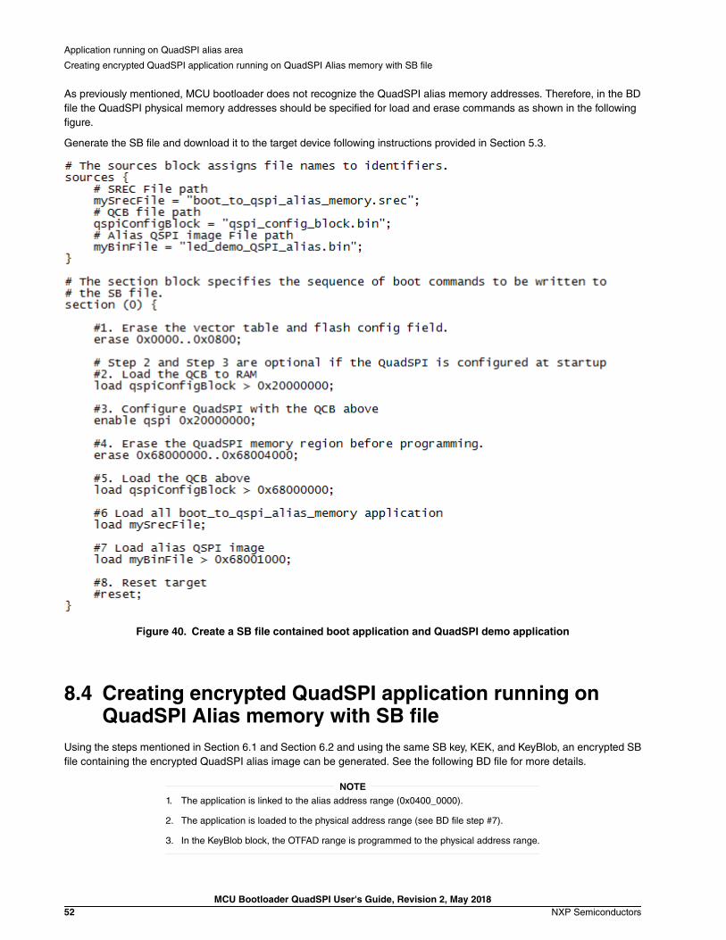
As previously mentioned, MCU bootloader does not recognize the QuadSPI alias memory addresses. Therefore, in the BDfile the QuadSPI physical memory addresses should be specified for load and erase commands as shown in the followingfigure.
Generate the SB file and download it to the target device following instructions provided in Section 5.3.
Figure 40. Create a SB file contained boot application and QuadSPI demo application
8.4 Creating encrypted QuadSPI application running onQuadSPI Alias memory with SB file
Using the steps mentioned in Section 6.1 and Section 6.2 and using the same SB key, KEK, and KeyBlob, an encrypted SBfile containing the encrypted QuadSPI alias image can be generated. See the following BD file for more details.
1. The application is linked to the alias address range (0x0400_0000).
2. The application is loaded to the physical address range (see BD file step #7).
3. In the KeyBlob block, the OTFAD range is programmed to the physical address range.
NOTE
Application running on QuadSPI alias area
Creating encrypted QuadSPI application running on QuadSPI Alias memory with SB file
MCU Bootloader QuadSPI User's Guide, Revision 2, May 201852 NXP Semiconductors

Figure 41. Create a SB file contained boot application and encrypted QuadSPI alias demo application
Application running on QuadSPI alias area
Creating encrypted QuadSPI application running on QuadSPI Alias memory with SB file
MCU Bootloader QuadSPI User's Guide, Revision 2, May 2018NXP Semiconductors 53

Chapter 9Appendix A - QuadSPI configuration procedure
For MCU bootloader, follow the below steps to perfrom QuadSPI configuration using the QCB data. The following figuredepicts the corresponding flow chart:
• Detect the location of QCB from either start address of QuadSPI memory or internal flash
• Configure QuadSPI pinmux based on the information from QCB
• Enable QuadSPI clock gate, prepare to configure QuadSPI registers
• Configure look-up table
• Configure QuadSPI registers such as AHB buffer size and DDR mode as needed
• Configure work mode of external SPI flash device, for example, Quad Mode or Octal Mode
• Additional configuration for external SPI flash device, if required in the QCB
Figure 42. QuadSPI Configuration Flow in MCU bootloader
Appendix A - QuadSPI configuration procedure
MCU Bootloader QuadSPI User's Guide, Revision 2, May 201854 NXP Semiconductors

Chapter 10Appendix B - Re-enter MCU bootloader underdirect boot mode
When direct boot is enabled in the BCA with bootFlags field set to 0xFE, ROM configures the QCB and jumps to the QuadSPIapplication image directly, bypassing the detection of active peripherals for firmware update from host. In this case, theQuadSPI application has to implement a workaround to invoke MCU bootloader when the host needs to update the applicationimage. The QuadSPI application has to detect boot pin (NMI pin) assertion by the user and if asserted can follow belowprocedure to invoke MCU bootloader:
1. Erase the first sector of the internal flash to clear the BCA. Note that the flash configuration field of the BCA may have tobe restored back, as shown in the code snippet in Figure 43.
2. Jump to the runBootloader() ROM API using the bootloader API tree pointer.
The following figure shows sample implementation of re-entry into bootloader from application code. The example code withthe package contains the implementation of this feature in the led_demo_QuadSPI application.
Figure 43. Implementation of re-entering MCU bootloader in application
Appendix B - Re-enter MCU bootloader under direct boot mode
MCU Bootloader QuadSPI User's Guide, Revision 2, May 2018NXP Semiconductors 55

Chapter 11Appendix C - Explore more features in QCB
Several more features of QuadSPI are supported by MCU bootloader such as parallel mode, continuous read mode, and soon. The following sections provide examples of generating QCB with these modes enabled.
11.1 Parallel modeThis section provides an example of generating a QCB with the parallel mode support. Pay attention to these key points:
• The sector size and page size should be twice the actual size for the parallel mode.
• The 'parallel_mode_enable' field in QCB must be set to 1.
• The Program command should be replaced by the Page Program command, as the QuadSPI module only supports single-pad parallel programming.
This is the example:
// This is the QCB for the use case that two MX25U3235F are connected to QuadSPI0A and QuadSPI0B ports.// Work under parallel modeconst qspi_config_t qspi_config_block = { .tag = kQspiConfigTag, .version = { .version = kQspiVersionTag }, .lengthInBytes = 512, .sflash_A1_size = 0x400000, // 4MB .sflash_B1_size = 0x400000, // 4MB .sclk_freq = kQspiSerialClockFreq_High, // High frequency .sflash_type = kQspiFlashPad_Quad, // SPI Flash devices work under quad-pad mode .sflash_port = kQspiPort_EnableBothPorts, // Both QSPI0A and QSPI0B are enabled. .busy_bit_offset = 0, // Busy offset is 0 .ddr_mode_enable = 0, // disable DDR mode .dqs_enable = 0, // Disable DQS feature .parallel_mode_enable = 1, // QuadSPI module work under parallel mode .pagesize = 512, // Page Size : 256 *2 = 512 bytes .sectorsize = 0x2000, // Sector Size: 4KB * 2 = 8KB .device_mode_config_en = 1, // configure quad mode for spi flash .device_cmd = 0x40, // Enable quad mode .write_cmd_ipcr = 0x05000000U, // IPCR indicating enable seqid (5<<24) .ips_command_second_divider = 3,// Set second divider for QSPI serial clock to 3 .look_up_table = { // Seq0: Quad Read (maximum supported freq: 104MHz) /* CMD: 0xEB - Quad Read, Single pad ADDR: 0x18 - 24bit address, Quad pads DUMMY: 0x06 - 6 clock cycles, Quad pads READ: 0x80 - Read 128 bytes, Quad pads JUMP_ON_CS: 0 */ [0] = 0x0A1804EB, [1] = 0x1E800E06, [2] = 0x2400,
// Seq1: Write Enable (maximum supported freq: 104MHz)
Appendix C - Explore more features in QCB
Parallel mode
MCU Bootloader QuadSPI User's Guide, Revision 2, May 201856 NXP Semiconductors

/* CMD: 0x06 - Write Enable, Single pad */ [4] = 0x406,
// Seq2: Erase All (maximum supported freq: 104MHz) /* CMD: 0x60 - Erase All chip, Single pad */ [8] = 0x460,
// Seq3: Read Status (maximum supported freq: 104MHz) /* CMD: 0x05 - Read Status, single pad READ: 0x01 - Read 1 byte */ [12] = 0x1c010405,
// Seq4: Page Program (maximum supported freq: 104MHz) /* CMD: 0x02 - Page Program, Single pad ADDR: 0x18 - 24bit address, Single pad WRITE: 0x40 - Write 64 bytes at one pass, Single pad (0x40 is ignored, because it will be overwritten by page size) */ [16] = 0x08180402, [17] = 0x2040,
// Seq5: Write status register to enable quad mode /* CMD: 0x01 - Write Status Register, single pad WRITE: 0x01 - Write 1 byte of data, single pad */ [20] = 0x20010401,
// Seq7: Erase Sector /* CMD: 0x20 - Sector Erase, single pad ADDR: 0x18 - 24 bit address, single pad */ [28] = 0x08180420,
// Seq8: Dummy /* CMD: 0 - Dummy command, used to force SPI flash to exit continuous read mode. unecessary here because the continous read mode isn't enabled. */ [32] = 0, }, };
The previous example must be placed in the <sdk_package>/middleware/mcu-boot/apps/
QCBGenerator/src folder.
NOTE
Appendix C - Explore more features in QCB
Parallel mode
MCU Bootloader QuadSPI User's Guide, Revision 2, May 2018NXP Semiconductors 57

11.2 Continuous read modeThe MX25U3235F supports the continuous read mode (performance enhance mode) to provide high performance reads.The important item to be configure ford this use case is:
• The Dummy LUT entry must be configured according to the condition of the exiting continuous read mode. Otherwise, thedevice fails to perform an erase or a program operation as it cannot exit this mode correctly.
The following is an example:
Only the flash device connected on the QuadSPI0 A1 supports this module.
NOTE
// This is the QCB for when two MX25U3235F are connected to QuadSPI0A and QuadSPI0B ports.// Work under parallel modeconst qspi_config_t qspi_config_block = { .tag = kQspiConfigTag, .version = { .version = kQspiVersionTag }, .lengthInBytes = 512, .sflash_A1_size = 0x400000, // 4MB .sclk_freq = kQspiSerialClockFreq_High, // High frequency .sflash_type = kQspiFlashPad_Quad, // SPI Flash devices work under quad-pad mode .sflash_port = kQspiPort_EnableBothPorts, // Both QSPI0A and QSPI0B are enabled. .busy_bit_offset = 0, // Busy offset is 0 .ddr_mode_enable = 0, // disable DDR mode .dqs_enable = 0, // Disable DQS feature .parallel_mode_enable = 1, // QuadSPI module work under parallel mode .pagesize = 512, // Page Size : 256 *2 = 512 bytes .sectorsize = 0x2000, // Sector Size: 4KB * 2 = 8KB .device_mode_config_en = 1, // configure quad mode for spi flash .device_cmd = 0x40, // Enable quad mode .write_cmd_ipcr = 0x05000000U, // IPCR indicating enable seqid (5<<24) .ips_command_second_divider = 3,// Set second divider for QSPI serial clock to 3 .look_up_table = { // Seq0: Quad Read (maximum supported freq: 104MHz) /* CMD: 0xEB - Quad Read, Single pad ADDR: 0x18 - 24bit address, Quad pads MODE: 0xA5 - Continuous read mode, Quad Pads DUMMY: 0x04 - 4 clock cycles, Quad pads READ: 0x80 - Read 128 bytes, Quad pads JUMP_ON_CS: 1 */ [0] = 0x0A1804EB, [1] = 0x0E04012A5, [2] = 0x24011E80,
// Seq1: Write Enable (maximum supported freq: 104MHz) /* CMD: 0x06 - Write Enable, Single pad */ [4] = 0x406,
// Seq2: Erase All (maximum supported freq: 104MHz) /*
Appendix C - Explore more features in QCB
Continuous read mode
MCU Bootloader QuadSPI User's Guide, Revision 2, May 201858 NXP Semiconductors
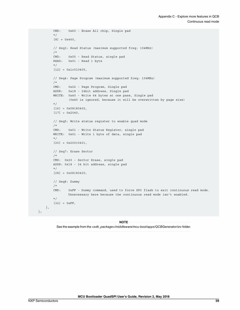
CMD: 0x60 - Erase All chip, Single pad */ [8] = 0x460,
// Seq3: Read Status (maximum supported freq: 104MHz) /* CMD: 0x05 - Read Status, single pad READ: 0x01 - Read 1 byte */ [12] = 0x1c010405,
// Seq4: Page Program (maximum supported freq: 104MHz) /* CMD: 0x02 - Page Program, Single pad ADDR: 0x18 - 24bit address, Single pad WRITE: 0x40 - Write 64 bytes at one pass, Single pad (0x40 is ignored, because it will be overwritten by page size) */ [16] = 0x08180402, [17] = 0x2040,
// Seq5: Write status register to enable quad mode /* CMD: 0x01 - Write Status Register, single pad WRITE: 0x01 - Write 1 byte of data, single pad */ [20] = 0x20010401,
// Seq7: Erase Sector /* CMD: 0x20 - Sector Erase, single pad ADDR: 0x18 - 24 bit address, single pad */ [28] = 0x08180420,
// Seq8: Dummy /* CMD: 0xFF - Dummy command, used to force SPI flash to exit continuous read mode. Unnecessary here because the continuous read mode isn't enabled. */ [32] = 0xFF, }, };
See the example from the <sdk_package>/middleware/mcu-boot/apps/QCBGenerator/src folder.
NOTE
Appendix C - Explore more features in QCB
Continuous read mode
MCU Bootloader QuadSPI User's Guide, Revision 2, May 2018NXP Semiconductors 59

Chapter 12Appendix D - DDR mode issue workaround
The MCU bootloader in the ROM of MK80F256 devices supports programming and booting from QuadSPI devices withdouble data rate (DDR) mode. However, due to an issue in the ROM code, a workaround is needed to use the DDR feature.This workaround should be implemented in the application image. This appendix provides the details on implementing theworkaround. The package contains example application code with the workaround implemented.
ROM provides DDR mode support using the values provided in the QCB data structure. Specifically, these two fields of QCBare used to support DDR mode:
• ddr_mode_enable - must be set to 1.
• data_hold_time - can be either 1 or 2 depending on the type of SPI Flash device.
1. This workaround is only applicable to ROM bootloader for K80, K81, K82, KL81, and KL82.
2. All QCB examples are applicable to both ROM bootloader and MCU bootloader 2.5.0.
NOTE
12.1 Example QCB for QuadSPI device N25Q256A with DDRmode support
The following is an example QCB for the N25Q256A with the DDR mode support:
const qspi_config_t qspi_config_block = { .tag = kQspiConfigTag, .version = { .version = kQspiVersionTag }, .lengthInBytes = 512, .sflash_A1_size = 0x2000000, // 32MB .sclk_freq = kQspiSerialClockFreq_High, // High frequency, 96MHz/4 = 24MHz .sflash_type = kQspiFlashPad_Quad, // SPI Flash devices work under quad-pad mode .sflash_port = kQspiPort_EnablePortA, // Only QSPI0A is enabled. .busy_bit_offset = 0x00010007, // Busy offset is 7, polarity: 0 means busy .ddr_mode_enable = 1, // Enable DDR mode .data_hold_time = 1, // Data aligned with 2x serial flash half clock .ddrsmp = 0, .dqs_enable = 0, // Disable DQS feature .dqs_loopback = 0, .pagesize = 256, // Page Size : 256 bytes .sectorsize = 0x1000, // Sector Size: 4KB .ips_command_second_divider = 0, .device_mode_config_en = 1, // Configure the device to 4-byte address mode .device_cmd = 0, // Not needed. .write_cmd_ipcr = 5UL<<24, // Seq5 for setting address type to 4 bytes
.look_up_table = { /* Seq0 : Quad Read (maximum supported freq: 108MHz) CMD_DDR: 0xED - Quad Read, Single pad ADDR_DDR: 0x20 - 32bit address, Quad pads DUMMY: 0x08 - 8 dummy cycles, Quad pads READ_DDR: 0x80 - Read 128 bytes, Quad pads JUMP_ON_CS: 0
Appendix D - DDR mode issue workaround
Example QCB for QuadSPI device N25Q256A with DDR mode support
MCU Bootloader QuadSPI User's Guide, Revision 2, May 201860 NXP Semiconductors

*/ [0] = 0x2A2004ED, [1] = 0x3A800E08, [2] = 0x2400,
/* Seq1: Write Enable (maximum supported freq: 108MHz) CMD: 0x06 - Write Enable, Single pad */ [4] = 0x406,
/* Seq2: Erase All (maximum supported freq: 108MHz) CMD: 0xC7 - Erase All chip, Single pad */ [8] = 0x04C7,
/* Seq3: Read Status (maximum supported freq: 108MHz) CMD: 0x05 - Read Flag Status, single pad READ: 0x04 - Read 4 bytes */ [12] = 0x1c040470,
/* Seq4: Page Program (maximum supported freq: 108MHz) CMD: 0x02 - Page Program, Single pad ADDR: 0x20 - 32bit address, Single pad WRITE: 0x40 - Write 64 bytes at one pass, Single Pad */ [16] = 0x08200402, [17] = 0x2040,
/* Seq5: Enter 4-byte address mode CMD: 0xB7 - Enter 4-byte address mode */ [20] = 0x04B7,
/* Seq7: Erase Sector CMD: 0x20 - Sector Erase, single pad ADDR: 0x20 - 32 bit address, single pad */ [28] = 0x08200420, }, };
See Section 3.3.3 to generate the binary qspi_config_block.bin file with the above example QCB data structures.
12.2 Example QCB for QuadSPI device S26KS128S withOctal DDR mode support
Here is another example QCB for the S26KS128S device with the Octal DDR mode support:
const qspi_config_t qspi_config_block ={ .tag = kQspiConfigTag, .version = {.version = kQspiVersionTag}, .lengthInBytes = 512, .word_addressable = 1, .data_hold_time = 1,
Appendix D - DDR mode issue workaround
Example QCB for QuadSPI device S26KS128S with Octal DDR mode support
MCU Bootloader QuadSPI User's Guide, Revision 2, May 2018NXP Semiconductors 61

.sflash_A1_size = 0x1000000, // 16MB .sclk_freq = kQspiSerialClockFreq_High, // High frequency, in DDR mode, it means 96MHz/4 = 24MHz .busy_bit_offset = 0x0001000F, // bit 15 represent busy bit, polarity of this bit is 0 .sflash_type = kQspiFlashPad_Octal, // Serial Nor Flash works under octal-pad mode .sflash_port = kQspiPort_EnablePortA, // Only PortA are enabled .ddr_mode_enable = 1, .dqs_enable = 1, // DQS function is enabled. .look_up_table = { // Seq0 : Read [0] = 0x2B1847A0, // Read command with continuous burst type [1] = 0x0F104F10, // 16bit column address, 16 dummy cycles [2] = 0x03003B80, // Read 128bytes and STOP.
// Seq1: Write Enable [4] = 0x2B184700, [5] = 0x47004F10, [6] = 0x4755,
// Seq2: Erase All [8] = 0x2B184700, [9] = 0x47004F10, [10] = 0x4710,
// Seq3: Read Status [12] = 0x2B1847A0, // Read command with continuous burst type [13] = 0x0F104F10, // 16bit column address, 16 dummy cycles [14] = 0x3B02, // Read 2bytes and stop.
// Seq4: 8 I/O Page Program [16] = 0x2B184700, [17] = 0x3F804F10,
// Seq6: Pre Erase [24] = 0x2B184700, [25] = 0x47004F10, [26] = 0x4780,
// Seq7: Erase Sector [28] = 0x2B184700, [29] = 0x47004F10, [30] = 0x24004730,
// Seq9: PreWriteEnable [36] = 0x2B184700, [37] = 0x47004F10, [38] = 0x47AA,
// Seq10: PrePageProgram [40] = 0x2B184700, [41] = 0x47004F10, [42] = 0x47A0,
// Seq11: PreReadStatus [44] = 0x2B184700, [45] = 0x47004F10, [46] = 0x4770,
} ,
Appendix D - DDR mode issue workaround
Example QCB for QuadSPI device S26KS128S with Octal DDR mode support
MCU Bootloader QuadSPI User's Guide, Revision 2, May 201862 NXP Semiconductors

.column_address_space = 3, .differential_clock_pin_enable = 1, // Differential clock is enabled. .dqs_latency_enable = 1, // External DQS input signal is used. .dqs_fa_delay_chain_sel = 0x10, .pagesize = 512, // Page Size: 512 bytes .sectorsize = 0x40000, // Sector Size: 256KB .ips_command_second_divider = 4,// Set second divider for QSPI serial clock to 16 .need_multi_phases = 1, // multiple phases are needed for Erase, Program, etc. .is_spansion_hyperflash = 1, // this device belongs to HyperFlash family. .pre_read_status_cmd_address_offset = 0x555<<1, .pre_unlock_cmd_address_offset = 0x555<<1, .unlock_cmd_address_offset = 0x2AA<<1, .pre_program_cmd_address_offset = 0x555<<1, .pre_erase_cmd_address_offset = 0x555<<1, .erase_all_cmd_address_offset = 0x555<<1, };
12.3 Changes to user application for implementing DDRmode path
The following subsections describe the steps required to map the led-demo to run from the external QuadSPI flash memoryin the DDR mode. See the led_demo_QSPI_patch project in the <sdk_package>/boards/<board>/bootloader_examples/demo_apps folder for more details.
12.3.1 Workaround solutionA workaround solution is required for the SPI flash devices with the DDR mode. The ROM missed a step in its implementationsteps to set the QuadSPI_FLSHCR [TDH], QuadSPI_SOCCR[DLYTAPSELA], and QuadSPI_SOCCR[DLYTAPSELB]register bit fields. Therefore, the workaround patch consists of a very small piece of code to set the missed bit fields beforejumping to the application image residing in the external QuadSPI flash memory. The patch function may reside in the internalflash memory.
The workaround patch function is defined with the following prototype in the package:
int rom_patch(uint32_t qcbBaseAddress);
The following code shows how the workaround patch function is implemented in the example project provided with thepackage:
int rom_patch(qspi_config_t *base) { volatile uint32_t *qspi_flshcr_reg = (volatile uint32_t*)QuadSPI0_FLSHCR_BASE; volatile uint32_t *qspi_soccr_reg = (volatile uint32_t*)QuadSPI0_SOCCR_BASE;
*qspi_flshcr_reg &= (uint32_t)~QuadSPI_FLSHCR_TDH_MASK; *qspi_flshcr_reg |= (base->data_hold_time)<<QuadSPI0_FLSHCR_TDH_SHIFT;
*qspi_soccr_reg &= (uint32_t)~QuadSPI0_SOCCR_DLYTAPSELA_MASK; *qspi_soccr_reg |= (base->dqs_fa_delay_chain_sel << QuadSPI0_SOCCR_DLYTAPSELA_SHIFT) & QuadSPI0_SOCCR_DLYTAPSELA_MASK; *qspi_soccr_reg &= (uint32_t)~QuadSPI0_SOCCR_DLYTAPSELB_MASK; *qspi_soccr_reg |= (base->dqs_fb_delay_chain_sel << QuadSPI0_SOCCR_DLYTAPSELB_SHIFT) & QuadSPI0_SOCCR_DLYTAPSELB_MASK;
Appendix D - DDR mode issue workaround
Changes to user application for implementing DDR mode path
MCU Bootloader QuadSPI User's Guide, Revision 2, May 2018NXP Semiconductors 63

return kStatus_Success; }
The binary position-independent code generated using the IAR compiler for the ROM patch function (available with thepackage) is shown here:
const uint8_t s_rom_patch[128] = { 0x10, 0xB5, 0x01, 0x00, 0x18, 0x4A, 0x10, 0x00, 0x18, 0x30, 0x18, 0x4B,0x1B, 0x68, 0xF0, 0x24, 0x24, 0x04, 0x1C, 0x40, 0x02, 0xD0, 0x16, 0x4A, 0x10, 0x00, 0x18, 0x30, 0x13, 0x68, 0x15, 0x4C, 0x1C, 0x40, 0x14, 0x60,0x13, 0x68, 0x0C, 0x69, 0x24, 0x04, 0x1C, 0x43, 0x14, 0x60, 0x02, 0x68, 0x11, 0x4B, 0x13, 0x40, 0x03, 0x60, 0xDA, 0x22, 0x52, 0x00, 0x89, 0x18,0x02, 0x68, 0x0B, 0x68, 0x1B, 0x04, 0xFC, 0x24, 0xA4, 0x03, 0x1C, 0x40, 0x14, 0x43, 0x04, 0x60, 0x02, 0x68, 0x0B, 0x4B, 0x13, 0x40, 0x03, 0x60,0x02, 0x68, 0x49, 0x68, 0x09, 0x06, 0xFC, 0x23, 0x9B, 0x05, 0x0B, 0x40, 0x13, 0x43, 0x03, 0x60, 0x00, 0x20, 0x10, 0xBD, 0x0C, 0xA0, 0x0D, 0x40,0x24, 0x80, 0x04, 0x40, 0x0C, 0xA0, 0x05, 0x40, 0xFF, 0xFF, 0xFC, 0xFF, 0xFF, 0xFF, 0xC0, 0xFF, 0xFF, 0xFF, 0xFF, 0xC0};
These are the limitations for this workaround solution:
1. The DDR commands are only allowed in a second QCB after invoking this rom_patch workaround.
2. The CRC check feature is not allowed to validate the integrity of the image on the QuadSPI memory.
3. The QCB must be placed at a specific location in the internal flash pointed to by the qspiConfigBlockPointer in the BCA.
12.3.2 Changes to linker fileUsing the led_demo_QSPI as a starting point and using the IAR project as an example, the first step is to update the linkerfile. Two separate sections are needed in the memory for this change. See the led_demo_QSPI_patch project in the led_demoprojects for more details.
define symbol m_rom_patch_code_start = 0x00000410;define symbol m_rom_patch_code_end = 0x0000050F;
define symbol m_rom_patch_handler_start= 0x00000510;define symbol m_rom_patch_handler_end = 0x00000FFF;
define region m_rom_pach_code_region = mem:[from m_rom_patch_code_start to m_rom_patch_code_end];define region m_rom_patch_handler_region = mem:[from m_rom_patch_handler_start to m_rom_patch_handler_end];
place in m_rom_patch_handler_region { readonly section BootloaderPatchHandler };
place in m_rom_pach_code_region {readonly section rom_patch_code };
The “m_rom_patch_handler_region” defined above is used for holding the section that contains the functions to invoke theROM patch function.
The “m_rom_patch_code_region” defined above is used for placing the section that contains the ROM patch code mentionedin the previous section.
Appendix D - DDR mode issue workaround
Changes to user application for implementing DDR mode path
MCU Bootloader QuadSPI User's Guide, Revision 2, May 201864 NXP Semiconductors

12.3.3 Changes to startup fileThe Reset_Handler must be placed in the internal flash (for example, placing it in m_rom_patch_handler_region) and theROM patch function must be called before the other functions when the QuadSPI application is executed. See the changesin the following figures.
Figure 44. Changes to startup file for DDR support
The ROM_Patchhandler is the function placed in the m_rom_patch_handler_region.
NOTE
12.3.4 Changes to system_MK82F25615.c fileThe ROM patch code must be placed in the internal flash. For example, place it into the rom_patch_code section. See thefollowing figure for these changes.
Appendix D - DDR mode issue workaround
Changes to user application for implementing DDR mode path
MCU Bootloader QuadSPI User's Guide, Revision 2, May 2018NXP Semiconductors 65

Figure 45. Definitions of ROM patch code in IAR project
The ROM_PatchHandler must be placed in the internal flash as well. For example, it can be placed in theBootloaderPatchHandler section. See the following figure for these changes.
Figure 46. Define ROM patch handler in IAR project
Appendix D - DDR mode issue workaround
Changes to user application for implementing DDR mode path
MCU Bootloader QuadSPI User's Guide, Revision 2, May 201866 NXP Semiconductors

12.4 Workaround block diagramThe following figure shows the flow of MCU bootloader using QuadSPI DDR patch workaround mechanism described earlierin provisioning the application image on the QuadSPI with DDR mode enabled.
Figure 47. Workaround provisioning image on QuadSPI memory in DDR mode
The following figure shows the flow of MCU bootloader using QuadSPI DDR patch workaround mechanism described earlierin booting the application image from the QuadSPI with DDR mode enabled.
Appendix D - DDR mode issue workaround
Workaround block diagram
MCU Bootloader QuadSPI User's Guide, Revision 2, May 2018NXP Semiconductors 67
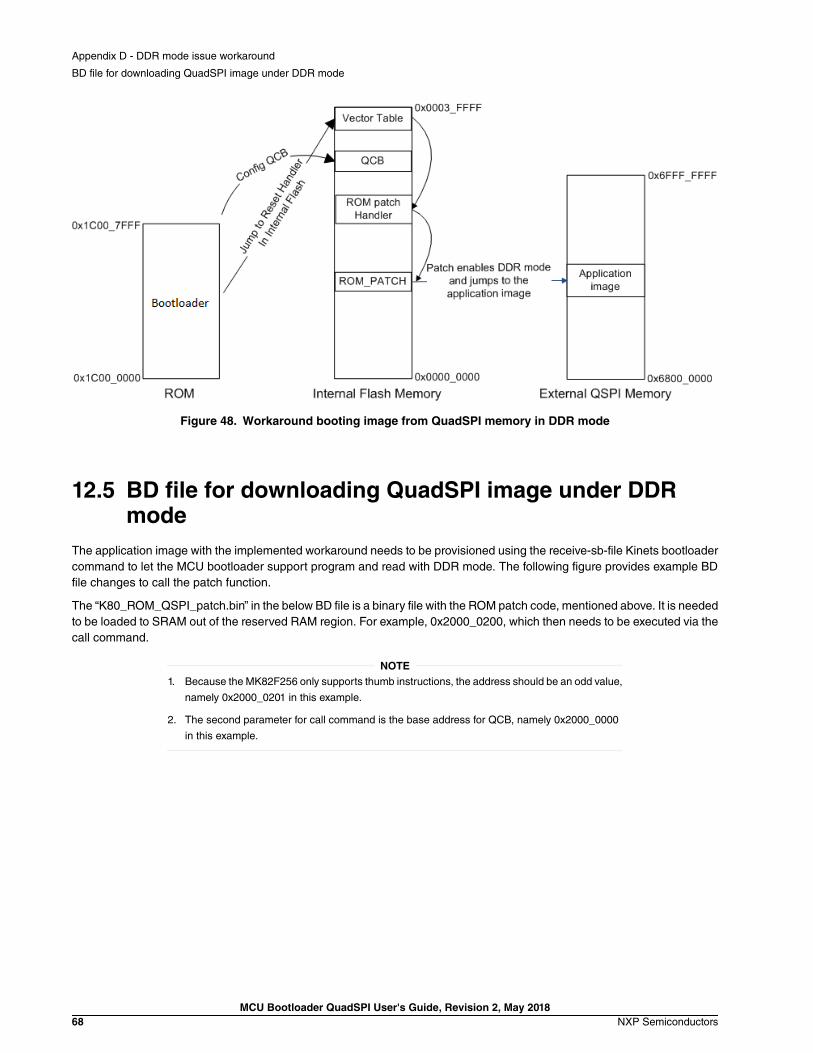
Figure 48. Workaround booting image from QuadSPI memory in DDR mode
12.5 BD file for downloading QuadSPI image under DDRmode
The application image with the implemented workaround needs to be provisioned using the receive-sb-file Kinets bootloadercommand to let the MCU bootloader support program and read with DDR mode. The following figure provides example BDfile changes to call the patch function.
The “K80_ROM_QSPI_patch.bin” in the below BD file is a binary file with the ROM patch code, mentioned above. It is neededto be loaded to SRAM out of the reserved RAM region. For example, 0x2000_0200, which then needs to be executed via thecall command.
1. Because the MK82F256 only supports thumb instructions, the address should be an odd value,
namely 0x2000_0201 in this example.
2. The second parameter for call command is the base address for QCB, namely 0x2000_0000
in this example.
NOTE
Appendix D - DDR mode issue workaround
BD file for downloading QuadSPI image under DDR mode
MCU Bootloader QuadSPI User's Guide, Revision 2, May 201868 NXP Semiconductors

Figure 49. BD file for invoking ROM patch for DDR mode
Appendix D - DDR mode issue workaround
BD file for downloading QuadSPI image under DDR mode
MCU Bootloader QuadSPI User's Guide, Revision 2, May 2018NXP Semiconductors 69

Chapter 13Revision history
The following table contains a history of changes made to this user's guide.
Table 5. Revision history
Revision number Date Substantive changes
0 09/2015 Initial release
1 04/2016 Kinetis Bootloader v2.0 release
2 05/2018 MCU Bootloader v2.5.0 release
Revision history
MCU Bootloader QuadSPI User's Guide, Revision 2, May 201870 NXP Semiconductors


How To Reach Us
Home Page:
nxp.com
Web Support:
nxp.com/support
Information in this document is provided solely to enable system and software implementers
to use NXP products. There are no express or implied copyright licenses granted hereunder
to design or fabricate any integrated circuits based on the information in this document. NXP
reserves the right to make changes without further notice to any products herein.
NXP makes no warranty, representation, or guarantee regarding the suitability of its products
for any particular purpose, nor does NXP assume any liability arising out of the application
or use of any product or circuit, and specifically disclaims any and all liability, including without
limitation consequential or incidental damages. “Typical” parameters that may be provided in
NXP data sheets and/or specifications can and do vary in different applications, and actual
performance may vary over time. All operating parameters, including “typicals,” must be
validated for each customer application by customer's technical experts. NXP does not convey
any license under its patent rights nor the rights of others. NXP sells products pursuant to
standard terms and conditions of sale, which can be found at the following address: nxp.com/
SalesTermsandConditions.
NXP, the NXP logo, NXP SECURE CONNECTIONS FOR A SMARTER WORLD, All other
product or service names are the property of their respective owners. ARM, AMBA, ARM
Powered, are registered trademarks of ARM Limited (or its subsidiaries) in the EU and/or
elsewhere. All rights reserved.
Ⓒ 2018 NXP B.V.