Embed Size (px)
Citation preview
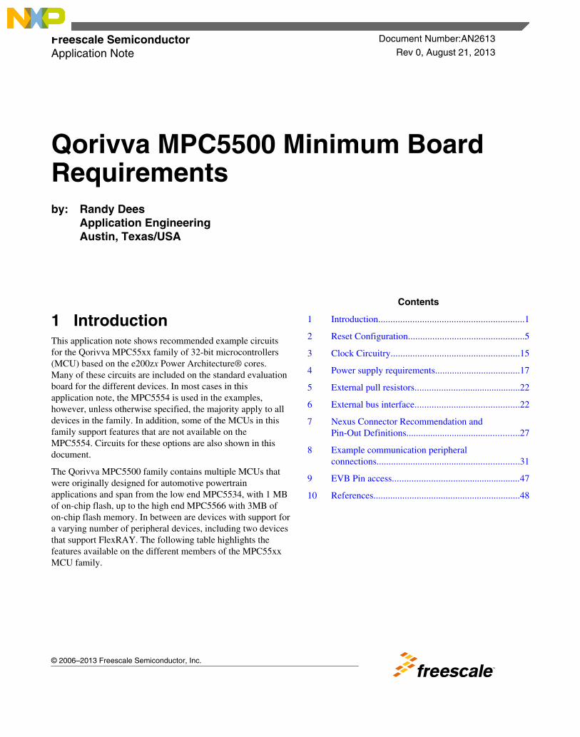
1 IntroductionThis application note shows recommended example circuitsfor the Qorivva MPC55xx family of 32-bit microcontrollers(MCU) based on the e200zx Power Architecture® cores.Many of these circuits are included on the standard evaluationboard for the different devices. In most cases in thisapplication note, the MPC5554 is used in the examples,however, unless otherwise specified, the majority apply to alldevices in the family. In addition, some of the MCUs in thisfamily support features that are not available on theMPC5554. Circuits for these options are also shown in thisdocument.
The Qorivva MPC5500 family contains multiple MCUs thatwere originally designed for automotive powertrainapplications and span from the low end MPC5534, with 1 MBof on-chip flash, up to the high end MPC5566 with 3MB ofon-chip flash memory. In between are devices with support fora varying number of peripheral devices, including two devicesthat support FlexRAY. The following table highlights thefeatures available on the different members of the MPC55xxMCU family.
Freescale Semiconductor Document Number:AN2613
Application Note Rev 0, August 21, 2013
Qorivva MPC5500 Minimum BoardRequirementsby: Randy Dees
Application EngineeringAustin, Texas/USA
© 2006–2013 Freescale Semiconductor, Inc.
Contents
1 Introduction............................................................1
2 Reset Configuration................................................5
3 Clock Circuitry.....................................................15
4 Power supply requirements...................................17
5 External pull resistors............................................22
6 External bus interface...........................................22
7 Nexus Connector Recommendation andPin-Out Definitions...............................................27
8 Example communication peripheralconnections...........................................................31
9 EVB Pin access.....................................................47
10 References.............................................................48
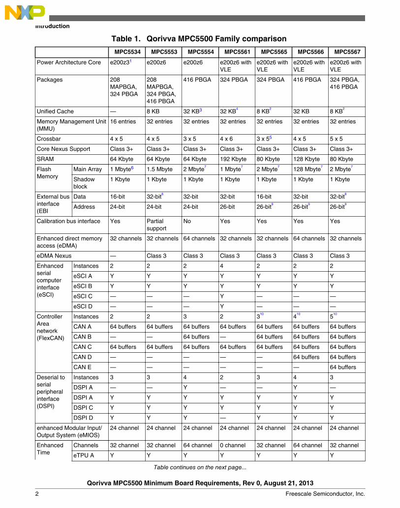
Table 1. Qorivva MPC5500 Family comparison
MPC5534 MPC5553 MPC5554 MPC5561 MPC5565 MPC5566 MPC5567
Power Architecture Core e200z31 e200z6 e200z6 e200z6 withVLE
e200z6 withVLE
e200z6 withVLE
e200z6 withVLE
Packages 208MAPBGA,324 PBGA
208MAPBGA,324 PBGA,416 PBGA
416 PBGA 324 PBGA 324 PBGA 416 PBGA 324 PBGA,416 PBGA
Unified Cache — 8 KB 32 KB3 32 KB4
8 KB2
32 KB 8 KB2
Memory Management Unit(MMU)
16 entries 32 entries 32 entries 32 entries 32 entries 32 entries 32 entries
Crossbar 4 x 5 4 x 5 3 x 5 4 x 6 3 x 55 4 x 5 5 x 5
Core Nexus Support Class 3+ Class 3+ Class 3+ Class 3+ Class 3+ Class 3+ Class 3+
SRAM 64 Kbyte 64 Kbyte 64 Kbyte 192 Kbyte 80 Kbyte 128 Kbyte 80 Kbyte
FlashMemory
Main Array 1 Mbyte6 1.5 Mbyte 2 Mbyte7
1 Mbyte7
2 Mbyte7
128 Mbyte7
2 Mbyte7
Shadowblock
1 Kbyte 1 Kbyte 1 Kbyte 1 Kbyte 1 Kbyte 1 Kbyte 1 Kbyte
External businterface(EBI
Data 16-bit 32-bit8
32-bit 32-bit 16-bit 32-bit 32-bit8
Address 24-bit 24-bit 24-bit 26-bit 26-bit9
26-bit9
26-bit9
Calibration bus interface Yes Partialsupport
No Yes Yes Yes Yes
Enhanced direct memoryaccess (eDMA)
32 channels 32 channels 64 channels 32 channels 32 channels 64 channels 32 channels
eDMA Nexus — Class 3 Class 3 Class 3 Class 3 Class 3 Class 3
Enhancedserialcomputerinterface(eSCI)
Instances 2 2 2 4 2 2 2
eSCI A Y Y Y Y Y Y Y
eSCI B Y Y Y Y Y Y Y
eSCI C — — — Y — — —
eSCI D — — — Y — — —
ControllerAreanetwork(FlexCAN)
Instances 2 2 3 2 310
410
510
CAN A 64 buffers 64 buffers 64 buffers 64 buffers 64 buffers 64 buffers 64 buffers
CAN B — — 64 buffers — 64 buffers 64 buffers 64 buffers
CAN C 64 buffers 64 buffers 64 buffers 64 buffers 64 buffers 64 buffers 64 buffers
CAN D — — — — — 64 buffers 64 buffers
CAN E — — — — — — 64 buffers
Deserial toserialperipheralinterface(DSPI)
Instances 3 3 4 2 3 4 3
DSPI A — — Y — — Y —
DSPI A Y Y Y Y Y Y Y
DSPI C Y Y Y Y Y Y Y
DSPI D Y Y Y — Y Y Y
enhanced Modular Input/Output System (eMIOS)
24 channel 24 channel 24 channel 24 channel 24 channel 24 channel 24 channel
EnhancedTime
Channels 32 channel 32 channel 64 channel 0 channel 32 channel 64 channel 32 channel
eTPU A Y Y Y Y Y Y Y
Table continues on the next page...
Introduction
Qorivva MPC5500 Minimum Board Requirements, Rev 0, August 21, 2013
2 Freescale Semiconductor, Inc.
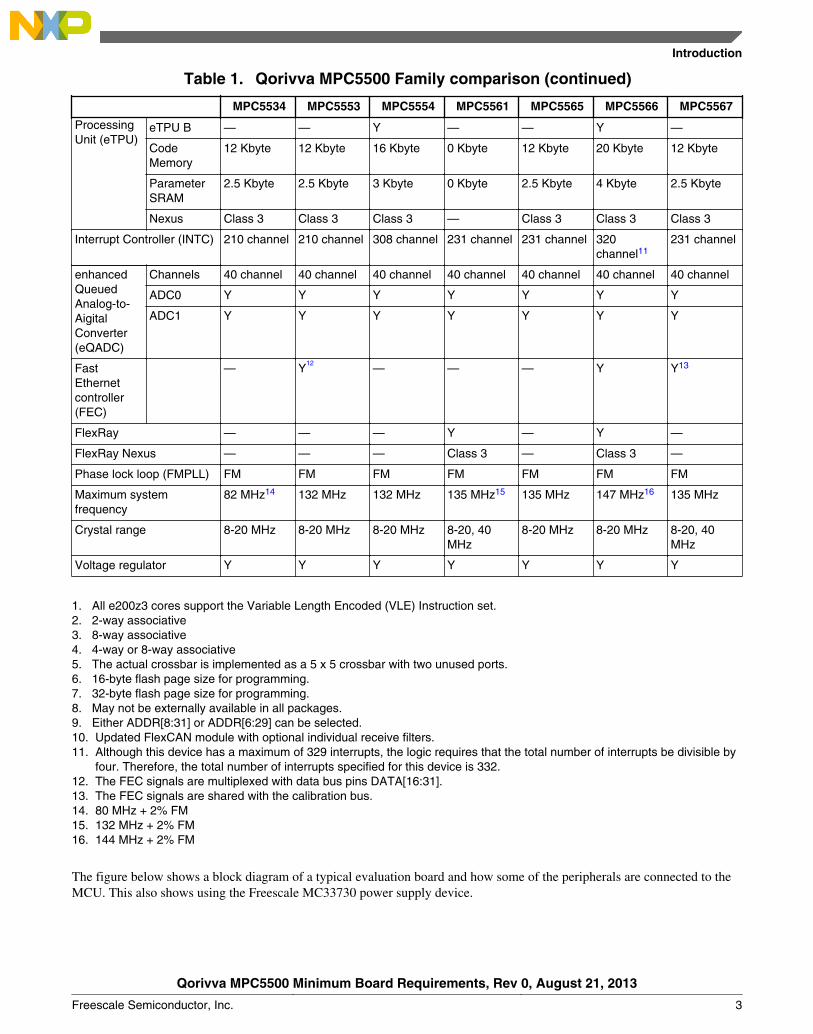
Table 1. Qorivva MPC5500 Family comparison (continued)
MPC5534 MPC5553 MPC5554 MPC5561 MPC5565 MPC5566 MPC5567
ProcessingUnit (eTPU)
eTPU B — — Y — — Y —
CodeMemory
12 Kbyte 12 Kbyte 16 Kbyte 0 Kbyte 12 Kbyte 20 Kbyte 12 Kbyte
ParameterSRAM
2.5 Kbyte 2.5 Kbyte 3 Kbyte 0 Kbyte 2.5 Kbyte 4 Kbyte 2.5 Kbyte
Nexus Class 3 Class 3 Class 3 — Class 3 Class 3 Class 3
Interrupt Controller (INTC) 210 channel 210 channel 308 channel 231 channel 231 channel 320channel11
231 channel
enhancedQueuedAnalog-to-AigitalConverter(eQADC)
Channels 40 channel 40 channel 40 channel 40 channel 40 channel 40 channel 40 channel
ADC0 Y Y Y Y Y Y Y
ADC1 Y Y Y Y Y Y Y
FastEthernetcontroller(FEC)
— Y12
— — — Y Y13
FlexRay — — — Y — Y —
FlexRay Nexus — — — Class 3 — Class 3 —
Phase lock loop (FMPLL) FM FM FM FM FM FM FM
Maximum systemfrequency
82 MHz14 132 MHz 132 MHz 135 MHz15 135 MHz 147 MHz16 135 MHz
Crystal range 8-20 MHz 8-20 MHz 8-20 MHz 8-20, 40MHz
8-20 MHz 8-20 MHz 8-20, 40MHz
Voltage regulator Y Y Y Y Y Y Y
1. All e200z3 cores support the Variable Length Encoded (VLE) Instruction set.2. 2-way associative3. 8-way associative4. 4-way or 8-way associative5. The actual crossbar is implemented as a 5 x 5 crossbar with two unused ports.6. 16-byte flash page size for programming.7. 32-byte flash page size for programming.8. May not be externally available in all packages.9. Either ADDR[8:31] or ADDR[6:29] can be selected.10. Updated FlexCAN module with optional individual receive filters.11. Although this device has a maximum of 329 interrupts, the logic requires that the total number of interrupts be divisible by
four. Therefore, the total number of interrupts specified for this device is 332.12. The FEC signals are multiplexed with data bus pins DATA[16:31].13. The FEC signals are shared with the calibration bus.14. 80 MHz + 2% FM15. 132 MHz + 2% FM16. 144 MHz + 2% FM
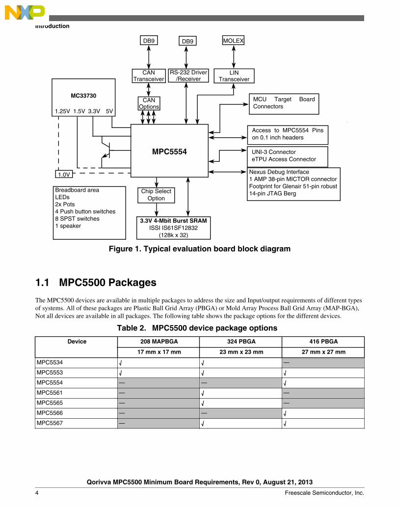
The figure below shows a block diagram of a typical evaluation board and how some of the peripherals are connected to theMCU. This also shows using the Freescale MC33730 power supply device.
Introduction
Qorivva MPC5500 Minimum Board Requirements, Rev 0, August 21, 2013
Freescale Semiconductor, Inc. 3
3.3V 4-Mbit Burst SRAMISSI IS61SF12832
(128k x 32)
Breadboard area LEDs 2x Pots 4 Push button switches 8 SPST switches 1 speaker
MPC5554
Chip Select Option
Nexus Debug Interface 1 AMP 38-pin MICTOR connector Footprint for Glenair 51-pin robust 14-pin JTAG Berg
LIN
1.0V
DB9
RS-232 Driver/Receiver Transceiver
MCU Target Board Connectors
MC33730
5V3.3V1.5V
CAN Options
DB9
1.25V
CANTransceiver
MOLEX
UNI-3 Connector eTPU Access Connector
Access to MPC5554 Pins on 0.1 inch headers
Figure 1. Typical evaluation board block diagram
1.1 MPC5500 Packages
The MPC5500 devices are available in multiple packages to address the size and Input/output requirements of different typesof systems. All of these packages are Plastic Ball Grid Array (PBGA) or Mold Array Process Ball Grid Array (MAP-BGA),Not all devices are available in all packages. The following table shows the package options for the different devices.
Table 2. MPC5500 device package options
Device 208 MAPBGA 324 PBGA 416 PBGA
17 mm x 17 mm 23 mm x 23 mm 27 mm x 27 mm
MPC5534 √ √ —
MPC5553 √ √ √
MPC5554 — — √
MPC5561 — √ —
MPC5565 — √ —
MPC5566 — — √
MPC5567 — √ √
Introduction
Qorivva MPC5500 Minimum Board Requirements, Rev 0, August 21, 2013
4 Freescale Semiconductor, Inc.

2 Reset ConfigurationSome operating features of the device are configured during reset. Depending on the value of the Reset Configuration pin(RSTCFG), either a default configuration is selected or external pins provide the configuration information. RSTCFG has aninternal pull up that will select the default settings unless driven from an external circuit or pulled down with an externaldevice strong enough to overcome the internal pull up. The following features are controllable via the reset configurationpins:
• Default configuration or externally controlled configuration (RSTCFG)• Boot mode: internal flash, external memory, or serial boot (BOOTCFG[0:1])• Clock Configuration: crystal oscillator or external reference clock (PLLCFG[0:1]), plus clock range (PLLCFG[2]1 )• Timer channel default pull (up or down) direction (WKPCFG)
The configuration pins (PLLCFG[0:1/2] and BOOTCFG[0:1]) are internally latched four clocks prior to the MCU negatingRSTOUT if RSTCFG is asserted. WKPCFG is always latched four clocks prior to RSTOUT negation and is not controlled bythe RSTCFG pin.
Depending on the system requirements, there are four recommended circuit options to support the reset configuration of thedevice. These are shown in the following table and are each described in later sections of this document.
Table 3. Recommended configuration circuit options
Desired ResetConfiguration Option
RSTCFGvalue
Clock Source Boot location Notes
Absolute minimum resetconfiguration (seeMinimum (default) RESETconfiguration circuit (mostcommonly used))
1 (high) Internal crystal oscillator Internal flash Uses internal crystaloscillator, boot frominternal flash
Full reset configurationcontrol1 (see ExternalRESET configuration withoptional GPIO on configpins)
0 (low) Internal crystal oscillator orexternal reference clock
Internal flash or externalmemory (selectable basedon desired configuration)
This configuration isrequired if theconfiguration pins2 areused for General PurposeInput/Outputs (GPIO)
Recommended minimumconfiguration when usingan external referenceclock with GPIO on configpins (see Minimumrequired circuitry forexternal reference clockmode (with optionalGPIO))
0 (low) External reference clock Internal flash or externalmemory (selectable basedon desired configuration)
Optionally, GPIO can beused with additionalcircuitry
Absolute minimumconfiguration for anexternal reference clockwithout GPIO on configpins (see Absoluteminimum RESETconfiguration circuit forexternal clock (GPIO onconfig pins not allowed))
0 (low) External reference clock Internal flash or externalmemory (selectable basedon desired configuration)
The Pad ConfigurationRegisters (PCR) for theconfiguration pins must beleft in their default states(GPIO not allowed on theconfiguration pins).
1. Not available on all devices.
Reset Configuration
Qorivva MPC5500 Minimum Board Requirements, Rev 0, August 21, 2013
Freescale Semiconductor, Inc. 5
1. Recommended for evaluation boards or initial prototypes to allow different configurations to be set.2. RSTCOFG, PLLCFG[0:1], and/or BOOTCFG[0:1]
The following table shows the default configuration that is selected if RSTCFG is negated (high).
Table 4. Default (RSTCFG = 1) configuration
Signals Value Selection
BOOTCFG[0:1] 0b00 Boot from internal flash
PLLCFG[0:1] 0b10 Use crystal oscillator
RSTCFG controls selection of either the default configuration or an external configuration as shown in the following table.
Table 5. Default (internal) versus external configuration control
RSTCFG Value Configuration mode
1 Default (internal) boot mode selected with a crystal oscillator reference. This provides the sameconfiguration as setting BOOTCFG[0:1]=0b00 and PLLCFG[0:1]=0b01
0 The values of BOOTCFG[0:1] and PLLCFG[0:1] control the boot and clock mode configuration
The following table shows the possible configurations of the memory boot mode.
Table 6. Boot memory configuration options
BOOTCFG[0] BOOTCFG[1] Boot mode
0 0 Boot from the internal flash memory (default when RSTCFG = 1)
0 1 Boot from FlexCAN or eSCI
1 0 Boot from the external memory (single master, with no arbitration)
1 1 Boot from the external memory (multi-master mode with external busarbitration). This mode is only supported on the MPC5554. It is notsupported on other devices.
The following table shows the options for the clock configuration that are controlled out of reset. On devices that supportPLLCFG[2], PLLCFG[2] is not latched and controls the predivider value of the PLL. PLLCFG[2] should only be high if a 40MHz crystal is used.
Table 7. PLL clock configuration
PLLCFG[0] PLLCFG[1] PLL Clock mode
0 0 Bypass mode
0 1 Normal mode with external reference clock
1 0 Normal mode with external crystal reference (uses internal oscillator). Thisis the default mode if RSTCFG = 1.
1 1 1:1 mode1
1. This mode is intended for use in dual controller systems only.
The default state of the enhanced Timing Processing Unit (eTPU) and the enhanced Modular Input/Output System (eMIOS)timer pins is controlled by the weak pull configuration pin (WKPCFG) as shown in the following table.
Reset Configuration
Qorivva MPC5500 Minimum Board Requirements, Rev 0, August 21, 2013
6 Freescale Semiconductor, Inc.

WKPCFG Weak Pull Configuration
0 eTPU and eMIOS pins have weak pull downs enabled.
1 eTPU and eMIOS pins have weak pull ups enabled.
NOTENot all eTPU and eMIOS pins are controlled by the WKPCFG pins. See the pindescriptions in the device Data Sheet and Reference Manual.
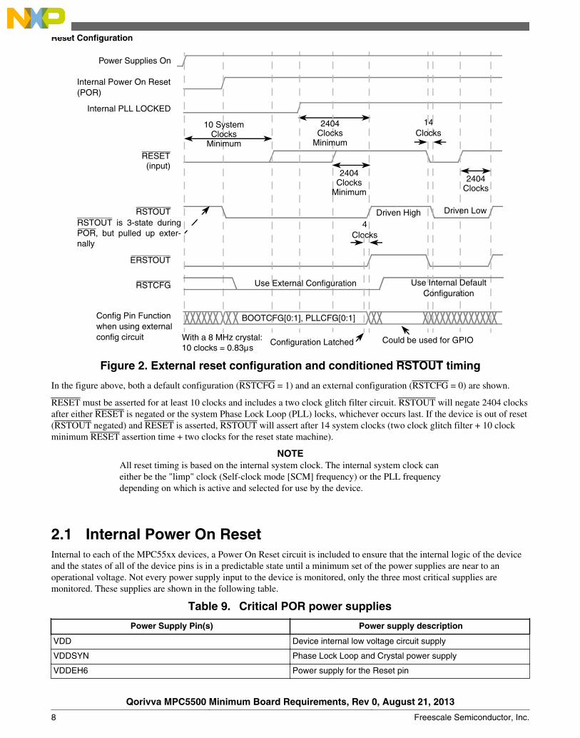
During the internal power on reset (POR) of the MPC5500 devices, the reset output pin ( RSTOUT) floats. A pull resistor onRSTOUT is required to control external circuitry during POR. Normally, a pull down should be used on RSTOUT to holdexternal circuitry in reset during POR. However, if an external configuration is required (for PLLCFG[1:0] andBOOTCFG[1:0]), then care needs to be taken. A possible, but extremely rare, misconfiguration can occur when the internalPOR negates2. There are multiple ways to address the requirements for external configuration depending on the systemrequirements such as external clock use and GPIO on the configuration pins. The examples in the external configurationsubsections of this document ensure that the errata will not be seen in the target system. Depending on the externalconfiguration circuitry, if RSTOUT has a pull up resistor to pull RSTOUT up during POR, then a conditioned external resetout (ERSTOUT) may be required for external devices that require RSTOUT to be low even during the internal POR time ofthe MCU. Freescale evaluation boards provide ERSTOUT that ANDs RESET and RSTOUT together. (The ERSTOUTcircuit is shown in external reset configuration sections, but can be used with the default [internal] reset configuration.)
The following figure shows the configuration pins under different power up scenarios. During POR, RSTOUT floats. TheRESET input to the MCU must be driven low by external Low Voltage Detect circuit before POR negates. The POR voltagetrip point is specified in the device data sheet (POR will negate on the MPC5554 between 1.1 and 1.35 volts for the 1.5 V(nominal) supply. Additionally, the device will be kept in the POR state until both the RESET pin power supply (VDDEH63 )and VDDSYN are between 2.0 V and 2.85 V. (VDDSYN will also assert the internal POR once it is powered to 0.3 volts.)
NOTEExternal low voltage detect (LVD) circuits must be used on all of the external powersupplies to ensure proper operation of the device. The external LVD circuitry must ensurethat the power supplies are within the recommended operating voltage prior to releasingthe RESET input to the MCU.
2. See errata number e488 (ERR000488/e488) on the device errata list.3. Although VDDEH6 is normally a 5 V supply, it can be used at a nominal voltage of 3.3 volts. Therefore the POR low
voltage detect must support 3.3 V operation, as well as 5 V operation.
Reset Configuration
Qorivva MPC5500 Minimum Board Requirements, Rev 0, August 21, 2013
Freescale Semiconductor, Inc. 7
, but pulled up exter- nally
RESET
Internal Power On Reset (POR)
ERSTOUT
RSTOUT is 3-state during POR
2404 Clocks
RSTOUT
BOOTCFG[0:1], PLLCFG[0:1]
Use External Configuration
10 System Clocks
Minimum
Power Supplies On
(input)
Driven High Driven Low
With a 8 MHz crystal: 10 clocks = 0.83μs
14 Clocks
RSTCFG Use Internal Default Configuration
Config Pin Function when using external config circuit
Internal PLL LOCKED
2404 Clocks
Minimum
2404 Clocks
Minimum
4 Clocks
Configuration Latched Could be used for GPIO
Figure 2. External reset configuration and conditioned RSTOUT timing
In the figure above, both a default configuration (RSTCFG = 1) and an external configuration (RSTCFG = 0) are shown.
RESET must be asserted for at least 10 clocks and includes a two clock glitch filter circuit. RSTOUT will negate 2404 clocksafter either RESET is negated or the system Phase Lock Loop (PLL) locks, whichever occurs last. If the device is out of reset(RSTOUT negated) and RESET is asserted, RSTOUT will assert after 14 system clocks (two clock glitch filter + 10 clockminimum RESET assertion time + two clocks for the reset state machine).
NOTEAll reset timing is based on the internal system clock. The internal system clock caneither be the "limp" clock (Self-clock mode [SCM] frequency) or the PLL frequencydepending on which is active and selected for use by the device.
2.1 Internal Power On ResetInternal to each of the MPC55xx devices, a Power On Reset circuit is included to ensure that the internal logic of the deviceand the states of all of the device pins is in a predictable state until a minimum set of the power supplies are near to anoperational voltage. Not every power supply input to the device is monitored, only the three most critical supplies aremonitored. These supplies are shown in the following table.
Table 9. Critical POR power supplies
Power Supply Pin(s) Power supply description
VDD Device internal low voltage circuit supply
VDDSYN Phase Lock Loop and Crystal power supply
VDDEH6 Power supply for the Reset pin
Reset Configuration
Qorivva MPC5500 Minimum Board Requirements, Rev 0, August 21, 2013
8 Freescale Semiconductor, Inc.
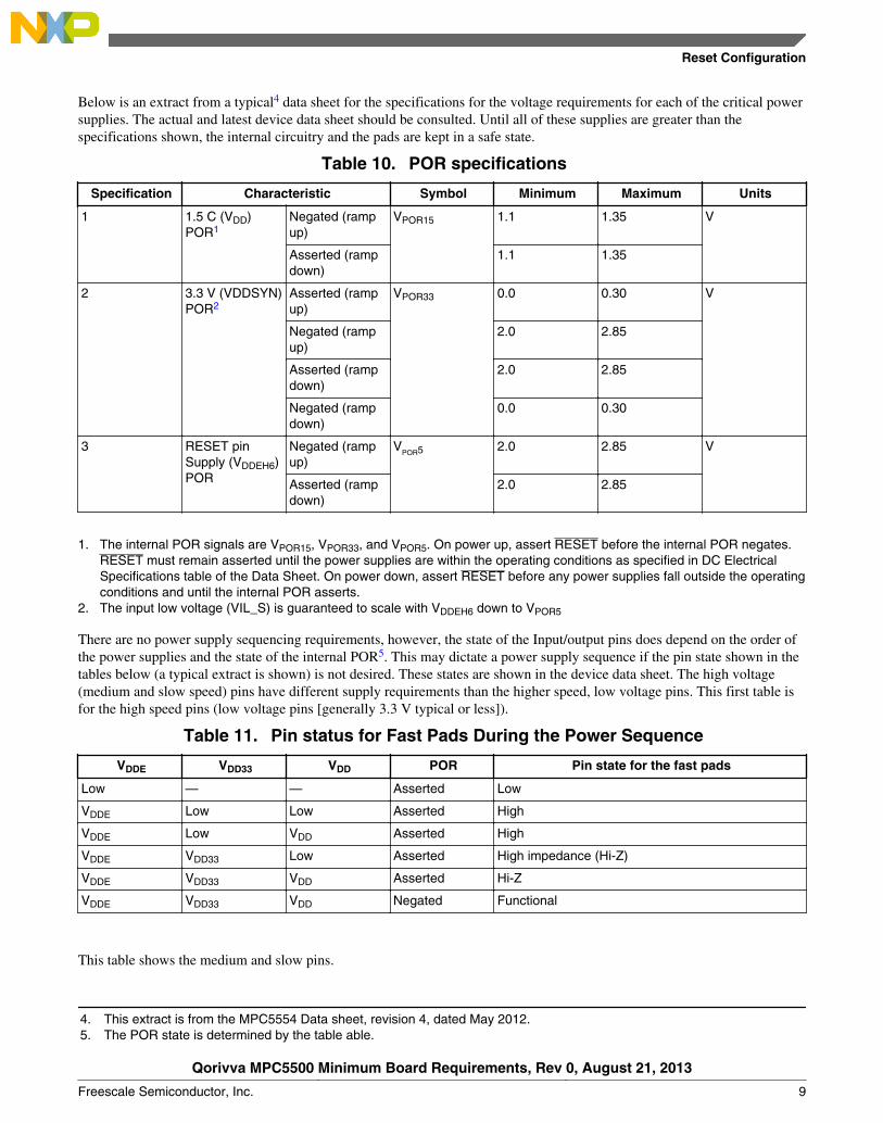
Below is an extract from a typical4 data sheet for the specifications for the voltage requirements for each of the critical powersupplies. The actual and latest device data sheet should be consulted. Until all of these supplies are greater than thespecifications shown, the internal circuitry and the pads are kept in a safe state.
Table 10. POR specifications
Specification Characteristic Symbol Minimum Maximum Units
1 1.5 C (VDD)POR1
Negated (rampup)
VPOR15 1.1 1.35 V
Asserted (rampdown)
1.1 1.35
2 3.3 V (VDDSYN)POR2
Asserted (rampup)
VPOR33 0.0 0.30 V
Negated (rampup)
2.0 2.85
Asserted (rampdown)
2.0 2.85
Negated (rampdown)
0.0 0.30
3 RESET pinSupply (VDDEH6)POR
Negated (rampup)
VPOR5 2.0 2.85 V
Asserted (rampdown)
2.0 2.85
1. The internal POR signals are VPOR15, VPOR33, and VPOR5. On power up, assert RESET before the internal POR negates.RESET must remain asserted until the power supplies are within the operating conditions as specified in DC ElectricalSpecifications table of the Data Sheet. On power down, assert RESET before any power supplies fall outside the operatingconditions and until the internal POR asserts.
2. The input low voltage (VIL_S) is guaranteed to scale with VDDEH6 down to VPOR5
There are no power supply sequencing requirements, however, the state of the Input/output pins does depend on the order ofthe power supplies and the state of the internal POR5. This may dictate a power supply sequence if the pin state shown in thetables below (a typical extract is shown) is not desired. These states are shown in the device data sheet. The high voltage(medium and slow speed) pins have different supply requirements than the higher speed, low voltage pins. This first table isfor the high speed pins (low voltage pins [generally 3.3 V typical or less]).
Table 11. Pin status for Fast Pads During the Power Sequence
VDDE VDD33 VDD POR Pin state for the fast pads
Low — — Asserted Low
VDDE Low Low Asserted High
VDDE Low VDD Asserted High
VDDE VDD33 Low Asserted High impedance (Hi-Z)
VDDE VDD33 VDD Asserted Hi-Z
VDDE VDD33 VDD Negated Functional
This table shows the medium and slow pins.
4. This extract is from the MPC5554 Data sheet, revision 4, dated May 2012.5. The POR state is determined by the table able.
Reset Configuration
Qorivva MPC5500 Minimum Board Requirements, Rev 0, August 21, 2013
Freescale Semiconductor, Inc. 9
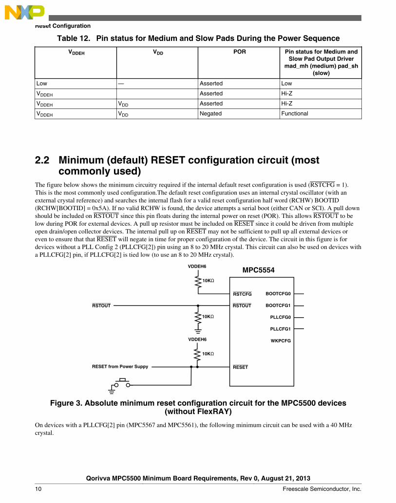
Table 12. Pin status for Medium and Slow Pads During the Power Sequence
VDDEH VDD POR Pin status for Medium andSlow Pad Output Driver
mad_mh (medium) pad_sh(slow)
Low — Asserted Low
VDDEH Asserted Hi-Z
VDDEH VDD Asserted Hi-Z
VDDEH VDD Negated Functional
2.2 Minimum (default) RESET configuration circuit (mostcommonly used)
The figure below shows the minimum circuitry required if the internal default reset configuration is used (RSTCFG = 1).This is the most commonly used configuration.The default reset configuration uses an internal crystal oscillator (with anexternal crystal reference) and searches the internal flash for a valid reset configuration half word (RCHW) BOOTID(RCHW[BOOTID] = 0x5A). If no valid RCHW is found, the device attempts a serial boot (either CAN or SCI). A pull downshould be included on RSTOUT since this pin floats during the internal power on reset (POR). This allows RSTOUT to below during POR for external devices. A pull up resistor must be included on RESET since it could be driven from multipleopen drain/open collector devices. The internal pull up on RESET may not be sufficient to pull up all external devices oreven to ensure that that RESET will negate in time for proper configuration of the device. The circuit in this figure is fordevices without a PLL Config 2 (PLLCFG[2]) pin using an 8 to 20 MHz crystal. This circuit can also be used on devices witha PLLCFG[2] pin, if PLLCFG[2] is tied low (to use an 8 to 20 MHz crystal).
Freescale Semiconductor6
BOOTCFG1
BOOTCFG0
PLLCFG0
PLLCFG1
RSTOUT
RSTCFG
WKPCFG
10KΩ
RESET
10KΩ
VDDEH6
10KΩ
VDDEH6
RSTOUT
MPC5554
RESET from Power Suppy
Figure 3. Absolute minimum reset configuration circuit for the MPC5500 devices(without FlexRAY)
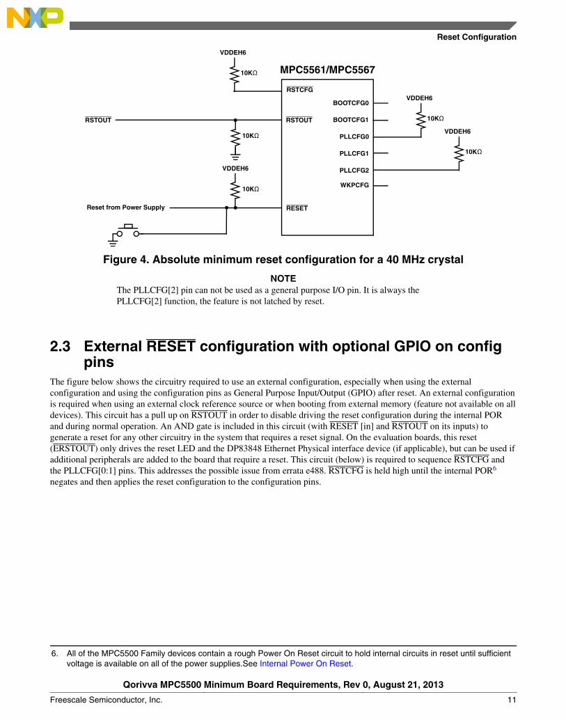
On devices with a PLLCFG[2] pin (MPC5567 and MPC5561), the following minimum circuit can be used with a 40 MHzcrystal.
Reset Configuration
Qorivva MPC5500 Minimum Board Requirements, Rev 0, August 21, 2013
10 Freescale Semiconductor, Inc.
BOOTCFG1
BOOTCFG0
PLLCFG0
PLLCFG1
RSTOUT
RSTCFG
PLLCFG2
10KΩ
RESET
10KΩ
VDDEH6
Reset from Power Supply
RSTOUT
MPC5561/MPC5567
10KΩ
VDDEH6
WKPCFG
10KΩ
VDDEH6
10KΩ
VDDEH6
Figure 4. Absolute minimum reset configuration for a 40 MHz crystal
NOTEThe PLLCFG[2] pin can not be used as a general purpose I/O pin. It is always thePLLCFG[2] function, the feature is not latched by reset.
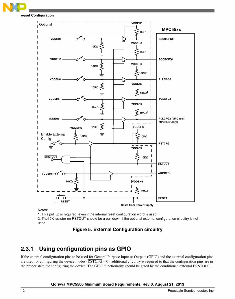
2.3 External RESET configuration with optional GPIO on configpins
The figure below shows the circuitry required to use an external configuration, especially when using the externalconfiguration and using the configuration pins as General Purpose Input/Output (GPIO) after reset. An external configurationis required when using an external clock reference source or when booting from external memory (feature not available on alldevices). This circuit has a pull up on RSTOUT in order to disable driving the reset configuration during the internal PORand during normal operation. An AND gate is included in this circuit (with RESET [in] and RSTOUT on its inputs) togenerate a reset for any other circuitry in the system that requires a reset signal. On the evaluation boards, this reset(ERSTOUT) only drives the reset LED and the DP83848 Ethernet Physical interface device (if applicable), but can be used ifadditional peripherals are added to the board that require a reset. This circuit (below) is required to sequence RSTCFG andthe PLLCFG[0:1] pins. This addresses the possible issue from errata e488. RSTCFG is held high until the internal POR6
negates and then applies the reset configuration to the configuration pins.
6. All of the MPC5500 Family devices contain a rough Power On Reset circuit to hold internal circuits in reset until sufficientvoltage is available on all of the power supplies.See Internal Power On Reset.
Reset Configuration
Qorivva MPC5500 Minimum Board Requirements, Rev 0, August 21, 2013
Freescale Semiconductor, Inc. 11
BOOTCFG1
BOOTCFG0
PLLCFG0
PLLCFG1
RSTOUT
RSTCFG
10KΩ
WKPCFG
10KΩ
10KΩ
10KΩ
VDDEH6
VDDEH6
VDDEH6
VDDEH6
VDDEH6
VDDEH610KΩ
10KΩ
10KΩ1
10KΩ1
10KΩ
VDDEH6
VDDEH6
RESET
10KΩ
VDDEH6
Reset from Power Supply
10KΩ2
VDDEH6
10KΩ1
VDDEH6
10KΩ
Notes: 1. This pull up is required, even if the internal reset configuration word is used. 2. The10K resistor on RSTOUT should be a pull down if the optional external configuration circuitry is not used.
VDDEH6
VDDEH6
Enable External Config
ERSTOUT
MPC55xx
RESET
PLLCFG2 (MPC5561, MPC5567 only)
VDDEH6
10KΩ1
10KΩ
VDDEH6
Optional
Figure 5. External Configuration circuitry
2.3.1 Using configuration pins as GPIOIf the external configuration pins to be used for General Purpose Input or Outputs (GPIO) and the external configuration pinsare used for configuring the device modes (RSTCFG = 0), additional circuitry is required to that the configuration pins are inthe proper state for configuring the device. The GPIO functionality should be gated by the conditioned external ERSTOUT.
Reset Configuration
Qorivva MPC5500 Minimum Board Requirements, Rev 0, August 21, 2013
12 Freescale Semiconductor, Inc.
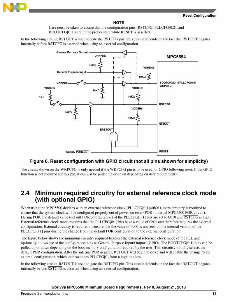
NOTECare must be taken to ensure that the configuration pins (RSTCFG, PLLCFG[0:2], andBOOTCFG[0:1]) are in the proper state while RESET is asserted.
In the following circuit, RSTOUT is used to gate the RSTCFG pin. This circuit depends on the fact that RSTOUT negatesinternally before RSTCFG is asserted when using an external configuration.
BOOTCFG[0:1]/PLLCFG[0:1]
RSTOUT
RSTCFG
VDDEH6
VDDEH6
10KΩ
10KΩ
VDDEH6
General Purpose Input
1KΩ
10KΩ
VDDEH6
10KΩ
VDDEH6
10KΩ
General Purpose OutputVDDEH6
10KΩ
RESET
ERSTOUT
Supply PORESET
MPC5554
WKPCFG
Figure 6. Reset configuration with GPIO circuit (not all pins shown for simplicity)
The circuit shown on the WKPCFG is only needed if the WKPCFG pin is to be used for GPIO following reset. If the GPIOfunction is not required for this pin, it can just be pulled up or down depending on user requirements.
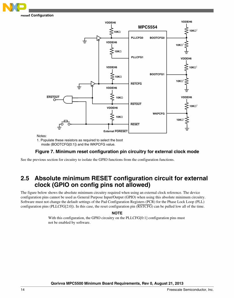
2.4 Minimum required circuitry for external reference clock mode(with optional GPIO)
When using the MPC5500 devices with an external reference clock (PLLCFG[0:1]=0b01), extra circuitry is required toensure that the system clock will be configured properly out of power-on reset (POR - internal MPC5500 POR circuit).During POR, the default value (default POR configuration) of the PLLCFG[0:1] bits are set to 0b10 and RSTCFG is high.External reference clock mode requires that the PLLCFG[0:1] bits have a value of 0b01 and therefore requires the externalconfiguration. External circuitry is required to ensure that the value of 0b00 is not seen on the internal version of thePLLCFG[0:1] pins during the change from the default POR configuration to the external configuration.
The figure below shows the minimum circuitry required to select the external reference clock mode of the PLL andoptionally allows use of the configuration pins as General Purpose Input/Outputs (GPIO). The BOOTCFG[0:1] pins can bepulled up or down depending on the boot memory configuration required by the user. This circuitry initially selects thedefault POR configuration. After the internal POR negates, RSTOUT will begin to drive and will enable the change to theexternal configuration, which then switches PLLCFG[0] from a high to a low.
In the following circuit, RSTOUT is used to gate the RSTCFG pin. This circuit depends on the fact that RSTOUT negatesinternally before RSTCFG is asserted when using an external configuration.
Reset Configuration
Qorivva MPC5500 Minimum Board Requirements, Rev 0, August 21, 2013
Freescale Semiconductor, Inc. 13
BOOTCFG1
BOOTCFG0 PLLCFG0
PLLCFG1
RSTOUT
RSTCFG
10KΩ1
WKPCFG
10KΩ1
10KΩ1
VDDEH6
VDDEH6
VDDEH6
10KΩ1
10KΩ
10KΩ
RESET
10KΩ
VDDEH6
External PORESET
10KΩ
VDDEH6
10KΩ
VDDEH6
Notes: 1. Populate these resistors as required to select the boot
mode (BOOTCFG[0:1]) and the WKPCFG value.
VDDEH6
ERSTOUT
10KΩ1
VDDEH6
10KΩ1
MPC5554
Figure 7. Minimum reset configuration pin circuitry for external clock mode
See the previous section for circuitry to isolate the GPIO functions from the configuration functions.
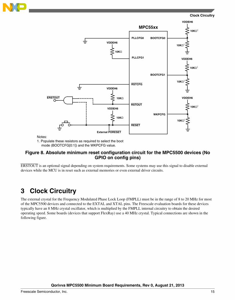
2.5 Absolute minimum RESET configuration circuit for externalclock (GPIO on config pins not allowed)
The figure below shows the absolute minimum circuitry required when using an external clock reference. The deviceconfiguration pins cannot be used as General Purpose Input/Output (GPIO) when using this absolute minimum circuitry.Software must not change the default settings of the Pad Configuration Registers (PCR) for the Phase Lock Loop (PLL)configuration pins (PLLCFG[2:0]). In this case, the reset configuration pin (RSTCFG) can be pulled low all of the time.
NOTEWith this configuration, the GPIO circuitry on the PLLCFG[0:1] configuration pins mustnot be enabled by software.
Reset Configuration
Qorivva MPC5500 Minimum Board Requirements, Rev 0, August 21, 2013
14 Freescale Semiconductor, Inc.
BOOTCFG1
BOOTCFG0 PLLCFG0
PLLCFG1
RSTOUT
RSTCFG
10KΩ1
WKPCFG
10KΩ1
10KΩ1
VDDEH6
VDDEH6
10KΩ1
10KΩ
RESET
10KΩ
VDDEH6
External PORESET
10KΩ
VDDEH6
Notes: 1. Populate these resistors as required to select the boot
mode (BOOTCFG[0:1]) and the WKPCFG value.
VDDEH6
ERSTOUT
10KΩ1
VDDEH6
10KΩ1
MPC55xx
Figure 8. Absolute minimum reset configuration circuit for the MPC5500 devices (NoGPIO on config pins)
ERSTOUT is an optional signal depending on system requirements. Some systems may use this signal to disable externaldevices while the MCU is in reset such as external memories or even external driver circuits.
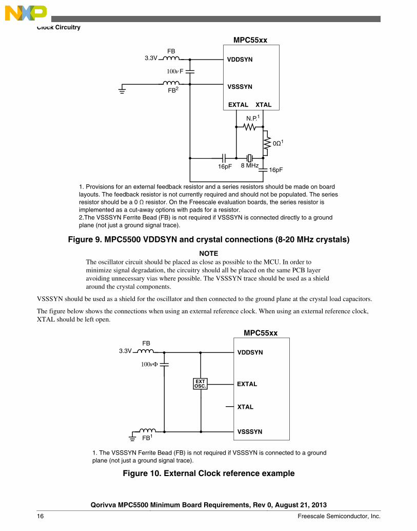
3 Clock CircuitryThe external crystal for the Frequency Modulated Phase Lock Loop (FMPLL) must be in the range of 8 to 20 MHz for mostof the MPC5500 devices and connected to the EXTAL and XTAL pins. The Freescale evaluation boards for these devicestypically have an 8 MHz crystal oscillator, which is multiplied by the FMPLL internal circuitry to obtain the desiredoperating speed. Some boards (devices that support FlexRay) use a 40 MHz crystal. Typical connections are shown in thefollowing figure.
Clock Circuitry
Qorivva MPC5500 Minimum Board Requirements, Rev 0, August 21, 2013
Freescale Semiconductor, Inc. 15
VDDSYN
MPC55xx
VSSSYN
3.3V
100nF
FB2
XTALEXTAL
16pF16pF 8 MHz
0Ω1
N.P.1
FB
1. Provisions for an external feedback resistor and a series resistors should be made on board layouts. The feedback resistor is not currently required and should not be populated. The series resistor should be a 0 Ω resistor. On the Freescale evaluation boards, the series resistor is implemented as a cut-away options with pads for a resistor. 2.The VSSSYN Ferrite Bead (FB) is not required if VSSSYN is connected directly to a ground plane (not just a ground signal trace).
Figure 9. MPC5500 VDDSYN and crystal connections (8-20 MHz crystals)
NOTEThe oscillator circuit should be placed as close as possible to the MCU. In order tominimize signal degradation, the circuitry should all be placed on the same PCB layeravoiding unnecessary vias where possible. The VSSSYN trace should be used as a shieldaround the crystal components.
VSSSYN should be used as a shield for the oscillator and then connected to the ground plane at the crystal load capacitors.
The figure below shows the connections when using an external reference clock. When using an external reference clock,XTAL should be left open.
VDDSYN
MPC55xx
VSSSYN
3.3V
100nF
FB1
EXTAL
1. The VSSSYN Ferrite Bead (FB) is not required if VSSSYN is connected to a ground plane (not just a ground signal trace).
EXT OSC.
XTAL
FB
Figure 10. External Clock reference example
Clock Circuitry
Qorivva MPC5500 Minimum Board Requirements, Rev 0, August 21, 2013
16 Freescale Semiconductor, Inc.

Some devices, such as the MPC5567 and the MPC5561 that support FlexRAY, also allow for a 40 MHz external crystalconfiguration. These devices include an additional configuration pin (PLLCFG[2]) to select between the 8-20 MHz crystal orthe 40 MHz crystal. PLLCFG2 does not exist and was used as VRCVSS on other devices (that do not support the 40 MHzoption). To select the 40 MHz option, PLLCFG[2] should be pulled or driven high.
NOTESetting PLLCFG[2] high forces the Predivider (set to divide-by-two) in the PLL to beselected by default, making the input to the PLL the same as the 8-20 MHz option.
When using the 40 MHz crystal, the buffered crystal frequency is available to be selected for the FlexRAY protocol clock.Similarly, the FlexCAN can also use the buffered crystal as a reference.
When a ferrite bead is used, it should have a low resistance at DC voltage with an increasing resistance at higher frequencies(100 MHz). The following table shows a recommended ferrite bead.
Table 13. Recommended ferrite bead
Manufacturer Part number DC resistance Impedance at100 Mhz, 20°C
Rated current Package size Operatingtemperature
range
Murata BLM31PG391SN1
0.05Ω 390Ω ±25% 20001 mA 1206 -55 to +125°C
1. 1000 mA at 125°C
4 Power supply requirementsThe MPC5500 devices require 5V, 3.3V, and 1.5V power supplies. The 1.5V can be generated using an on-chip regulatorcontroller with a linear external pass transistor.
The table below lists the supplies required by the MPC5500. Many of the supply pins can be used over a wide voltage range.Low voltage supplies generally can be used at nominal voltage ranges from 1.8 to 3.3 V and high voltage supplies can use anominal 3.3 or 5 V supply. There are several supplies that must be a particular voltage (either 3.3 V or 5 V). The simplestboard configuration uses 3.3 V and 5 V as the main external supplies and uses the internal 1.5 V regulator controller. Themost commonly used configuration uses a bus voltage of 3.3 V and all peripheral I/O modules at 5.0 V. Due to power supplysegmenting, some peripheral power supplies can be used at 3.3 V and some at 5 V if required, as long as the pins are ondifferent power supply segments. The I/O voltage is the same for all pins sharing a common power supply segment. Inaddition, if standby SRAM operation is required (SRAM is kept powered while all of the other supplies are off), a 1.0 VSRAM standby supply should be provided.
Table 14. MPC5500 power supply requirements
Symbol Description Voltage range1 Maximum current2
VDDE_H External I/O Supply Input 3.3V-5.0V 40 mA3
VPP Flash program/erase supplyinput
5.0V 35 mA
VDDA Analog power input 5.0V 25 mA
VDDE, VDD33, VDDSYN External "low" voltage I/Osupply input
1.8V-3.3V 15 mA
VRC33 Voltage Regulator Controlsupply
3.3V 320 mA
VFLASH Flash read supply input 3.3V 4 mA
Table continues on the next page...
Power supply requirements
Qorivva MPC5500 Minimum Board Requirements, Rev 0, August 21, 2013
Freescale Semiconductor, Inc. 17
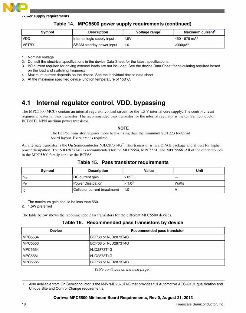
Table 14. MPC5500 power supply requirements (continued)
Symbol Description Voltage range1 Maximum current2
VDD Internal logic supply input 1.5V 450 - 875 mA4
VSTBY SRAM standby power input 1.0 <300µA5
1. Nominal voltage2. Consult the electrical specifications in the device Data Sheet for the latest specifications.3. I/O current required for driving external loads are not included. See the device Data Sheet for calculating required based
on the load and switching frequency.4. Maximum current depends on the device. See the individual device data sheet.5. At the maximum specified device junction temperature of 150°C.
4.1 Internal regulator control, VDD, bypassingThe MPC5500 MCUs contain an internal regulator control circuit for the 1.5 V internal core supply. The control circuitrequires an external pass transistor. The recommended pass transistor for the internal regulator is the On SemiconductorBCP68T1 NPN medium power transistor.
NOTEThe BCP68 transistor requires more heat-sinking than the minimum SOT223 footprintboard layout. Extra area is required.
An alternate transistor is the On Semiconductor NJD2873T4G7. This transistor is in a DPAK package and allows for higherpower dissipation. The NJD2873T4G is recommended for the MPC5554, MPC5561, and MPC5566. All of the other devicesin the MPC5500 family can use the BCP68.
Table 15. Pass transistor requirements
Symbol Description Value Unit
hFE DC current gain > 851 —
PD Power Dissipation > 1.02 Watts
IC Collector current (maximum) 1.0 A
1. The maximum gain should be less than 550.2. 1.5W preferred
The table below shows the recommended pass transistors for the different MPC5500 devices.
Table 16. Recommended pass transistors by device
Device Recommended pass transistor
MPC5534 BCP68 or NJD2873T4G
MPC5553 BCP68 or NJD2873T4G
MPC5554 NJD2873T4G
MPC5561 NJD2873T4G
MPC5565 BCP68 or NJD2873T4G
Table continues on the next page...
7. Also available from On Semiconductor is the MJVNJD2873T4G that provides full Automotive AEC-Q101 qualification andUnique Site and Control Change requirements.
Power supply requirements
Qorivva MPC5500 Minimum Board Requirements, Rev 0, August 21, 2013
18 Freescale Semiconductor, Inc.
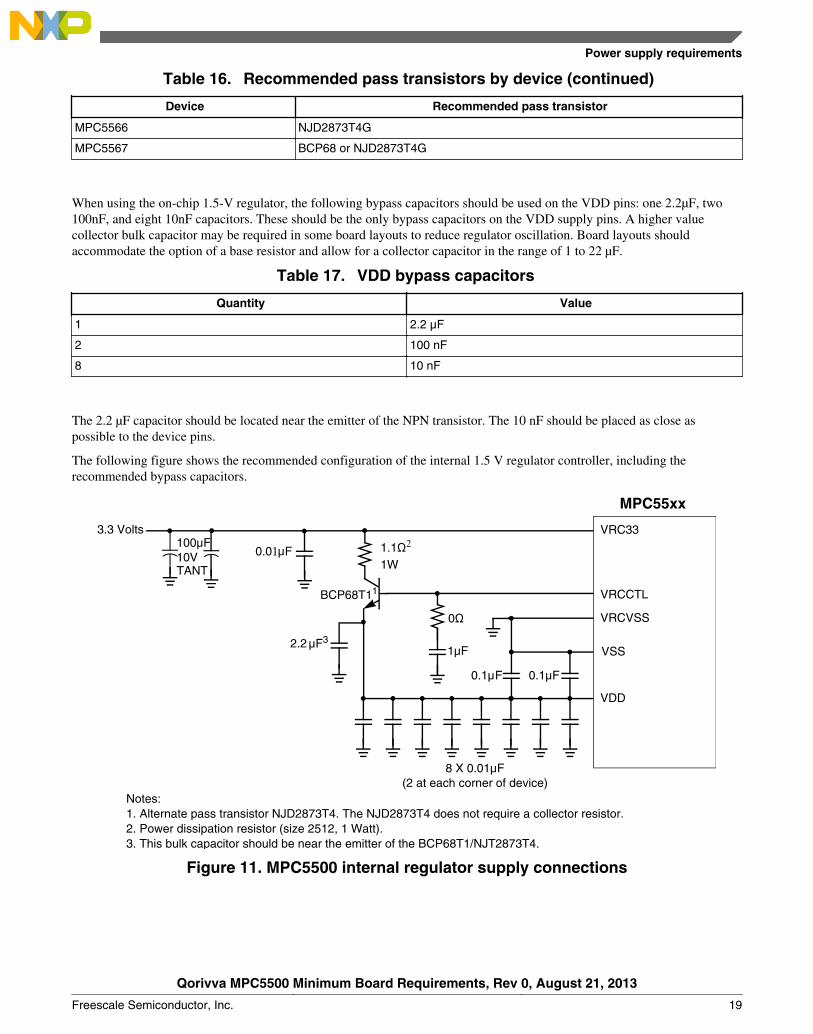
Table 16. Recommended pass transistors by device (continued)
Device Recommended pass transistor
MPC5566 NJD2873T4G
MPC5567 BCP68 or NJD2873T4G
When using the on-chip 1.5-V regulator, the following bypass capacitors should be used on the VDD pins: one 2.2µF, two100nF, and eight 10nF capacitors. These should be the only bypass capacitors on the VDD supply pins. A higher valuecollector bulk capacitor may be required in some board layouts to reduce regulator oscillation. Board layouts shouldaccommodate the option of a base resistor and allow for a collector capacitor in the range of 1 to 22 µF.
Table 17. VDD bypass capacitors
Quantity Value
1 2.2 µF
2 100 nF
8 10 nF
The 2.2 µF capacitor should be located near the emitter of the NPN transistor. The 10 nF should be placed as close aspossible to the device pins.
The following figure shows the recommended configuration of the internal 1.5 V regulator controller, including therecommended bypass capacitors.
3.3 Volts VRC33
VRCCTL
VRCVSS
VSS
VDD
BCP68T11
Notes: 1. Alternate pass transistor NJD2873T4. The NJD2873T4 does not require a collector resistor. 2. Power dissipation resistor (size 2512, 1 Watt). 3. This bulk capacitor should be near the emitter of the BCP68T1/NJT2873T4.
100μF 10V TANT
0.01 F
0.1μF0.1μ
2.2μF3
8 X 0.01μF (2 at each corner of device)
1.1Ω2
1W
MPC55xx
0Ω
1μF
F
μ
Figure 11. MPC5500 internal regulator supply connections
Power supply requirements
Qorivva MPC5500 Minimum Board Requirements, Rev 0, August 21, 2013
Freescale Semiconductor, Inc. 19

4.2 VDDSYN considerationsVDDSYN is the power supply for the oscillator and the clock Frequency Modulated Phase Lock Loop (FMPLL or PLL forshort). VDDSYN should be filtered separately from the rest of the 3.3 V power supplies to reduce both noise on the main 3.3V supply and to prevent noise from the 3.3 V supply affecting the stability of the PLL.
4.3 External memory power requirementsIf external memories are included in the final system, the currents need to be provided from the system power supply. Themaximum currents for the SRAM devices included in this application note are shown in the following table.
Table 18. External memory power requirements
Memory Part number Voltage (V) Maximum Current (mA)
Cypress SRAM CY7C1338 3.3V 375 mA
ISSI SRAM IS61SF12832 3.3V 280 mA
ISSI SRAM IS61SF25618 3.3V 170 mA
4.4 Decoupling capacitorsLocal decoupling capacitors should be used on every MCU power supply pin. Many of the capacitors can be mounted on theunderside of the PCB and should be located as close as possible to the respective power pins. In addition to the MCU, allother IC devices should have decoupling capacitors close to each power supply pin. Although not used on the MPC5500evaluation boards, Dupont™ has developed an embedded capacitor board process that uses the entire power and groundplaces of the PCB for capacitors. This uses their Interra™ HK 10 planar capacitor laminate (approximately 2nF per squareinch) and could be used to eliminate some of the localized bypass capacitors8. See AN2705 "Signal Integrity Considerationswith MPC5500-based systems" and AN2706 "EMC Guidelines for MPC5500-based Systems" for more information onbypass capacitors for the power supplies.
4.5 Enhanced Queued Analog to Digital Converter supplyconnections
The enhanced Queued Analog to Digital Converter (eQADC) should use a filtered power supply separate from the digital 5V.On the MPC5500 evaluation boards, a separate 5 V supply is used as a separate filtered analog supply for the eQADC.Filtered reference supplies should be provided for high and low voltage references (VRH and VRL). The impedance of thetraces of the following analog differential pairs should be matched: AN0/AN1, AN2/AN3, AN4/AN5 and AD6/AN7.
Unused Analog inputs should be pulled to ground.
The following figure shows the proper connections of the eQADC power supply connections.For best noise performance, thevoltage reference high and low pins (VRH, VRL) should be filtered and kept clean.
8. Due to cost, these typically are not used in Automotive applications, but is mentioned for other types of applications thatmay need a reduced set of external components.
Power supply requirements
Qorivva MPC5500 Minimum Board Requirements, Rev 0, August 21, 2013
20 Freescale Semiconductor, Inc.
10 μF
All bypass capacitors should be connected as close as possible to the device.
VSSA0
REFBYPC
VDDA0
VRH
10 ηF
100 ηF
VSSA1
VDDA1
10 ηF
VRL
10 μF
Analog 5V
10 ηF
FB
FB
FB
FB
VDDEH9
ANxAnalog Input
DANx+Differential Analog Input +
DANx-Differential Analog Input -
10 ηF
10 ηF
10 ηF
10 ηF
100 KΩ11. Layout for this resistor must be included for backwards compatibility and possible future changes.
Digital 5V
Note - This could be the location of the connection between Analog 5V and Digital 5V. If AN12:15 are used for Analog sig- nals, VDDEH9 should be filtered as if an ana- log supply.
MPC5554
Figure 12. MPC5500 Preferred eQADC supply bypassing
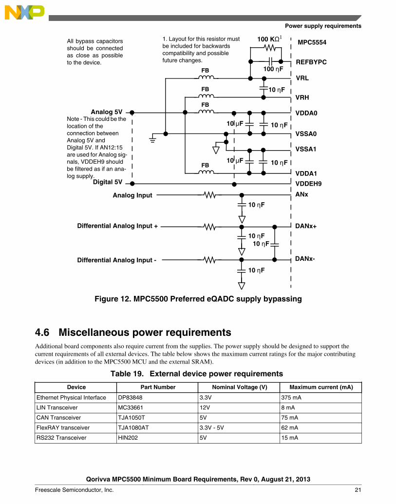
4.6 Miscellaneous power requirementsAdditional board components also require current from the supplies. The power supply should be designed to support thecurrent requirements of all external devices. The table below shows the maximum current ratings for the major contributingdevices (in addition to the MPC5500 MCU and the external SRAM).
Table 19. External device power requirements
Device Part Number Nominal Voltage (V) Maximum current (mA)
Ethernet Physical Interface DP83848 3.3V 375 mA
LIN Transceiver MC33661 12V 8 mA
CAN Transceiver TJA1050T 5V 75 mA
FlexRAY transceiver TJA1080AT 3.3V - 5V 62 mA
RS232 Transceiver HIN202 5V 15 mA
Power supply requirements
Qorivva MPC5500 Minimum Board Requirements, Rev 0, August 21, 2013
Freescale Semiconductor, Inc. 21
5 External pull resistorsExcept in the cases documented in this application note, external pull up or down resistors are not required on any pins,except to over ride the default state of the pins. After reset, the state of the pull device is controlled by the pad configurationregister in the System Integration Unit (SIU_PCR0–SIU_PCR230) for that pin. The direction of the internal pull device isdocumented in the device Data Sheet and Reference Manual, however, the setting can be changed by software in the PCRregister for each pin.
5.1 Bus control pinsUnless the MPC5500 device is not in multi-processor mode (BOOTCFG[0:1] = 0b11, RSTCFG = 0b0), the bus control pinsare not enabled. This allows minimum configuration boards to eliminate pull up resistors on the Bus request (BR), Bus Grant(BG), and Bus Busy (BB) pins. Normally, external pull ups are not required on the Transfer Acknowledge (TA) and TransferError Acknowledge (TEA) signals, but pull ups have been included on the MPC5500 evaluation board to handle situationswhere they might be required.
5.2 Timer pinsFollowing reset, all of the enhanced Modular Input/Output System (eMIOS) and enhanced Timing Processor Unit (eTPU)pins have a default state based on the WKPCFG pin. If WKPCFG is high, then the timer pins have pull ups and pull downs ifWKPCFG is low. If the state of some of these pins needs to be over-ridden during reset, an external pull is required that has avalue strong enough to overcome the internal 130µA pull current. WKPCFG is latched 4 clocks prior to the negation ofRSTOUT by the MCU.
5.3 Other pinsTo ensure that the internal factory test modes are not entered accidentally, a strong pull up (1-2KΩ) can be placed on theTEST pin to VDDE7 (usually 3.3 V). This is the same power supply as the Nexus pins. Unused pins should be configuredwith both the input and the output buffers turned off, but with the weak pull downs enabled.
6 External bus interfaceThe MPC5500 devices in most packages include a 32-bit wide external data bus with up to a 26-bit address bus. On somedevices, however, the package limits the data bus to only 16-bits and in other cases, does not support any access to anexternal data or address bus. An address bus of 20-bits is supported on all devices that support an external bus, however,some devices support an address bus of up to 24-bits and in some cases 26-bit, for the external address bus. On the Freescaleevaluation boards, the external bus is used for access to SRAM only. The external bus could also be connected to a variety ofother devices, such as stand-alone Flash memories or peripherals (either fast or slow9 ). When using the Ethernet interface onthe MPC5553 and MPC5566 on the MPC5553 evaluation board, only a 16-bit data bus is available. The MPC5534 andMPC5565 always have only a 16-bit data bus. The address bus width for the different devices in the MPC5500 family isshown in the following table.
9. Keep in mind, however, that accesses to the external bus stalls the core CPU any time data is read from the external bus.
External pull resistors
Qorivva MPC5500 Minimum Board Requirements, Rev 0, August 21, 2013
22 Freescale Semiconductor, Inc.
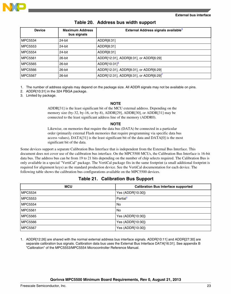
Table 20. Address bus width support
Device Maximum Addressbus signals
External Address signals available1
MPC5534 24-bit ADDR[8:31]
MPC5553 24-bit ADDR[8:31]
MPC5554 24-bit ADDR[8:31]
MPC5561 26-bit ADDR[12:31], ADDR[8:31], or ADDR[6:29]
MPC5565 26-bit ADDR[10:31]3
MPC5566 26-bit ADDR[12:31], ADDR[8:31], or ADDR[6:29]
MPC5567 26-bit ADDR[12:31], ADDR[8:31], or ADDR[6:29]2
1. The number of address signals may depend on the package size. All ADDR signals may not be available on pins.2. ADDR[10:31] in the 324 PBGA package.3. Limited by package.
NOTEADDR[31] is the least significant bit of the MCU external address. Depending on thememory size (by-32, by-16, or by-8), ADDR[29], ADDR[30], or ADDR[31] may beconnected to the least significant address line of the memory (ADDR0).
NOTELikewise, on memories that require the data bus (DATA) be connected in a particularorder (primarily external Flash memories that require programming via specific data busaccess values), DATA[31] is the least significant bit of the data and DATA[0] is the mostsignificant bit of the data.
Some devices support a separate Calibration Bus Interface that is independent from the External Bus Interface. Thisdocument does not cover use of the calibration bus interface. On the MPC5500 MCUs, the Calibration Bus Interface is 16-bitdata bus. The address bus can be from 19 to 21 bits depending on the number of chip selects required. The Calibration Bus isonly available in a special "VertiCal" package. The VertiCal package fits in the same footprint (a small additional footprint isrequired for alignment keys) as the standard production device. See the VertiCal documentation for each device. Thefollowing table shows the calibration bus configurations available on the MPC5500 devices.
Table 21. Calibration Bus Support
MCU Calibration Bus Interface supported
MPC5534 Yes (ADDR[10:30])
MPC5553 Partial1
MPC5554 No
MPC5561 No
MPC5565 Yes (ADDR[10:30])
MPC5566 Yes (ADDR[10:30])
MPC5567 Yes (ADDR[10:30])
1. ADDR[12:26] are shared with the normal external address bus interface signals. ADDR[10:11] and ADDR[27:30] areseparate calibration bus signals. Calibration data bus uses the External Bus Interface DATA[16:31]. See appendix B"Calibration" of the MPC5553/MPC5554 Microcontroller Reference Manual.
External bus interface
Qorivva MPC5500 Minimum Board Requirements, Rev 0, August 21, 2013
Freescale Semiconductor, Inc. 23
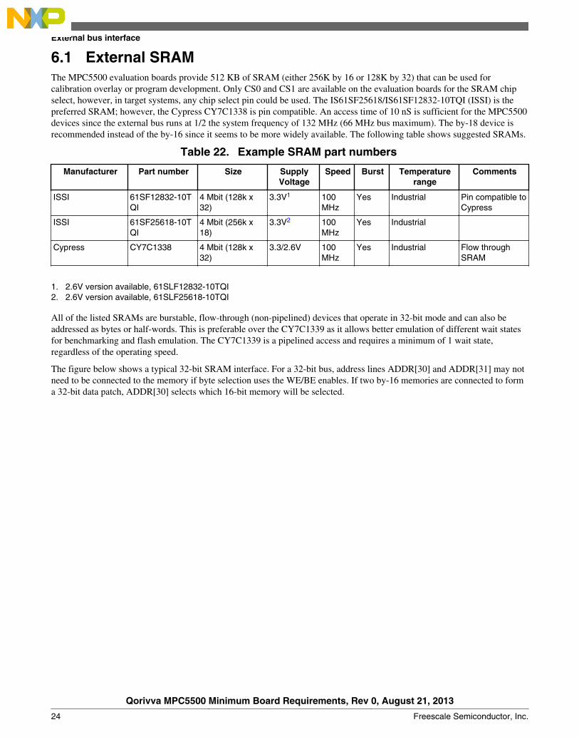
6.1 External SRAMThe MPC5500 evaluation boards provide 512 KB of SRAM (either 256K by 16 or 128K by 32) that can be used forcalibration overlay or program development. Only CS0 and CS1 are available on the evaluation boards for the SRAM chipselect, however, in target systems, any chip select pin could be used. The IS61SF25618/IS61SF12832-10TQI (ISSI) is thepreferred SRAM; however, the Cypress CY7C1338 is pin compatible. An access time of 10 nS is sufficient for the MPC5500devices since the external bus runs at 1/2 the system frequency of 132 MHz (66 MHz bus maximum). The by-18 device isrecommended instead of the by-16 since it seems to be more widely available. The following table shows suggested SRAMs.
Table 22. Example SRAM part numbers
Manufacturer Part number Size SupplyVoltage
Speed Burst Temperaturerange
Comments
ISSI 61SF12832-10TQI
4 Mbit (128k x32)
3.3V1 100MHz
Yes Industrial Pin compatible toCypress
ISSI 61SF25618-10TQI
4 Mbit (256k x18)
3.3V2 100MHz
Yes Industrial
Cypress CY7C1338 4 Mbit (128k x32)
3.3/2.6V 100MHz
Yes Industrial Flow throughSRAM
1. 2.6V version available, 61SLF12832-10TQI2. 2.6V version available, 61SLF25618-10TQI
All of the listed SRAMs are burstable, flow-through (non-pipelined) devices that operate in 32-bit mode and can also beaddressed as bytes or half-words. This is preferable over the CY7C1339 as it allows better emulation of different wait statesfor benchmarking and flash emulation. The CY7C1339 is a pipelined access and requires a minimum of 1 wait state,regardless of the operating speed.
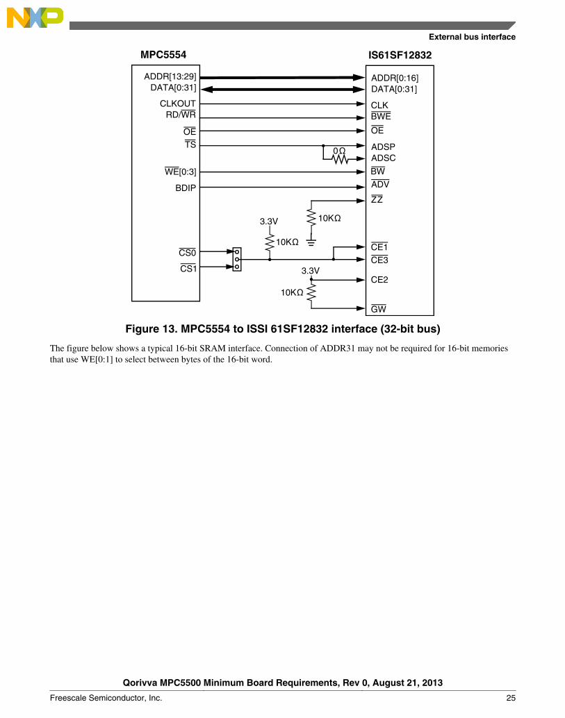
The figure below shows a typical 32-bit SRAM interface. For a 32-bit bus, address lines ADDR[30] and ADDR[31] may notneed to be connected to the memory if byte selection uses the WE/BE enables. If two by-16 memories are connected to forma 32-bit data patch, ADDR[30] selects which 16-bit memory will be selected.
External bus interface
Qorivva MPC5500 Minimum Board Requirements, Rev 0, August 21, 2013
24 Freescale Semiconductor, Inc.
ADDR[13:29] DATA[0:31]
OE
TS
WE[0:3]
BDIP
CS1
ADDR[0:16] DATA[0:31]
OE
ADSP ADSC
ADV
CE3
3.3V
MPC5554 IS61SF12832
GW
3.3V
CE1
CE2
10KΩ
ZZ
CLKOUT RD/WR
CS0
CLK BWE
BW
10KΩ
10KΩ
0Ω
Figure 13. MPC5554 to ISSI 61SF12832 interface (32-bit bus)
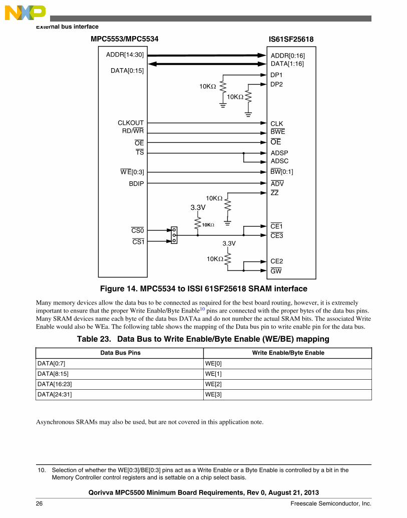
The figure below shows a typical 16-bit SRAM interface. Connection of ADDR31 may not be required for 16-bit memoriesthat use WE[0:1] to select between bytes of the 16-bit word.
External bus interface
Qorivva MPC5500 Minimum Board Requirements, Rev 0, August 21, 2013
Freescale Semiconductor, Inc. 25
ADDR[14:30]
DATA[0:15]
OE
TS
WE[0:3]
BDIP
CS1
ADDR[0:16] DATA[1:16]
OE
ADSP ADSC
BW[0:1]
CE3
3.3V
MPC5553/MPC5534
GW
3.3V
ZZ
CE1
CE2
10KΩ
10KΩ
DP1
DP2
IS61SF25618
ADV
CLKOUT RD/WR
CS0
CLK BWE
10KΩ
10KΩ10KΩ
Figure 14. MPC5534 to ISSI 61SF25618 SRAM interface
Many memory devices allow the data bus to be connected as required for the best board routing, however, it is extremelyimportant to ensure that the proper Write Enable/Byte Enable10 pins are connected with the proper bytes of the data bus pins.Many SRAM devices name each byte of the data bus DATAa and do not number the actual SRAM bits. The associated WriteEnable would also be WEa. The following table shows the mapping of the Data bus pin to write enable pin for the data bus.
Table 23. Data Bus to Write Enable/Byte Enable (WE/BE) mapping
Data Bus Pins Write Enable/Byte Enable
DATA[0:7] WE[0]
DATA[8:15] WE[1]
DATA[16:23] WE[2]
DATA[24:31] WE[3]
Asynchronous SRAMs may also be used, but are not covered in this application note.
10. Selection of whether the WE[0:3]/BE[0:3] pins act as a Write Enable or a Byte Enable is controlled by a bit in theMemory Controller control registers and is settable on a chip select basis.
External bus interface
Qorivva MPC5500 Minimum Board Requirements, Rev 0, August 21, 2013
26 Freescale Semiconductor, Inc.
6.2 External bus terminationHigh speed signals should either be terminated or laid out with a fixed impedance of approximately 33Ω. On the MPC5500evaluation boards, only the Clock Out (CLKOUT) pin is terminated. CLKOUT runs in two directions on the evaluationboard, through a series terminating resistor (in a very short trace to the SRAM) and is fully terminated at the end of the tracethat runs to the Nexus connectors. The Engineering Clock (ENGCLK) has series termination only.
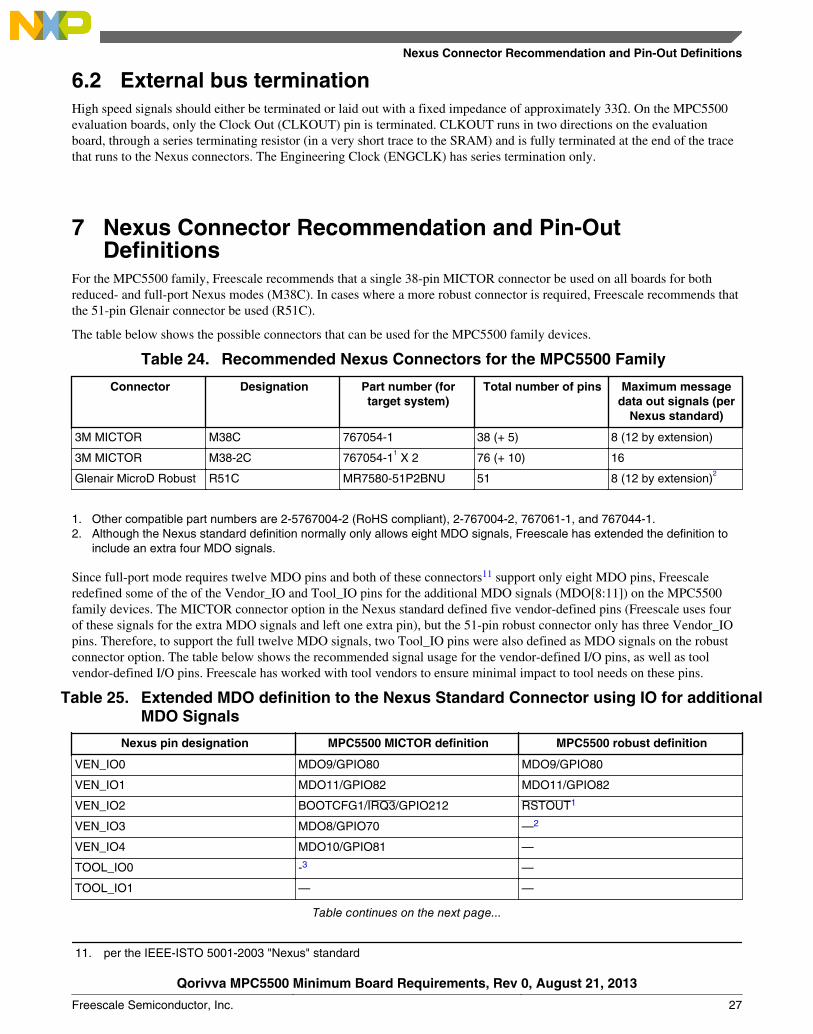
7 Nexus Connector Recommendation and Pin-OutDefinitions
For the MPC5500 family, Freescale recommends that a single 38-pin MICTOR connector be used on all boards for bothreduced- and full-port Nexus modes (M38C). In cases where a more robust connector is required, Freescale recommends thatthe 51-pin Glenair connector be used (R51C).
The table below shows the possible connectors that can be used for the MPC5500 family devices.
Table 24. Recommended Nexus Connectors for the MPC5500 Family
Connector Designation Part number (fortarget system)
Total number of pins Maximum messagedata out signals (per
Nexus standard)
3M MICTOR M38C 767054-1 38 (+ 5) 8 (12 by extension)
3M MICTOR M38-2C 767054-11 X 2 76 (+ 10) 16
Glenair MicroD Robust R51C MR7580-51P2BNU 51 8 (12 by extension)2
1. Other compatible part numbers are 2-5767004-2 (RoHS compliant), 2-767004-2, 767061-1, and 767044-1.2. Although the Nexus standard definition normally only allows eight MDO signals, Freescale has extended the definition to
include an extra four MDO signals.
Since full-port mode requires twelve MDO pins and both of these connectors11 support only eight MDO pins, Freescaleredefined some of the of the Vendor_IO and Tool_IO pins for the additional MDO signals (MDO[8:11]) on the MPC5500family devices. The MICTOR connector option in the Nexus standard defined five vendor-defined pins (Freescale uses fourof these signals for the extra MDO signals and left one extra pin), but the 51-pin robust connector only has three Vendor_IOpins. Therefore, to support the full twelve MDO signals, two Tool_IO pins were also defined as MDO signals on the robustconnector option. The table below shows the recommended signal usage for the vendor-defined I/O pins, as well as toolvendor-defined I/O pins. Freescale has worked with tool vendors to ensure minimal impact to tool needs on these pins.
Table 25. Extended MDO definition to the Nexus Standard Connector using IO for additionalMDO Signals
Nexus pin designation MPC5500 MICTOR definition MPC5500 robust definition
VEN_IO0 MDO9/GPIO80 MDO9/GPIO80
VEN_IO1 MDO11/GPIO82 MDO11/GPIO82
VEN_IO2 BOOTCFG1/IRQ3/GPIO212 RSTOUT1
VEN_IO3 MDO8/GPIO70 —2
VEN_IO4 MDO10/GPIO81 —
TOOL_IO0 -3 —
TOOL_IO1 — —
Table continues on the next page...
11. per the IEEE-ISTO 5001-2003 "Nexus" standard
Nexus Connector Recommendation and Pin-Out Definitions
Qorivva MPC5500 Minimum Board Requirements, Rev 0, August 21, 2013
Freescale Semiconductor, Inc. 27
Table 25. Extended MDO definition to the Nexus Standard Connector using IO for additionalMDO Signals (continued)
Nexus pin designation MPC5500 MICTOR definition MPC5500 robust definition
TOOL_IO2 — MDO8/GPIO70
TOOL_IO3 RSTOUT MDO10/GPIO81
1. This pin has been redefined since the original definition in 2004. Customers may want to make this signal selectable (via a0 Ω resistor option) between RSTOUT and BOOTCFG1/IRQ3/GPIO212.
2. This signal is not available on the 51-pin robust connector3. This pin is defined for use by tool vendors and has no defined connection to the MPC5500 device for the MICTOR
connector option.
7.1 MICTOR Connector Definition for the MPC5500 FamilyThe following table shows the complete signal usage for the MPC5500 full-port mode MICTOR connector. This uses theVendor_IO pins 1–4 as MDO[11:8]. This connector may also be used for reduced-port mode (which only uses MDO[3:0]).While only one MICTOR connector is recommended, some tools may not support this configuration. For maximum toolcompatibility, a second MICTOR connector may need to be added for the upper four MDO signals (MDO[11:8]).
Table 26. MPC5500 Family MICTOR Connector M38C
MPC5500 signal Combined M38Cor M38-2C
Combined M38Cor M38-2C
MPC5500 signal
- Reserved - 1
Gro
und 2 - Reserved
1-
- Reserved1
- 3 4 - Reserved1
-
MDO9/GPIO80 VEN_IO0 Out 5 6 Out CLOCKOUT CLKOUT
BOOTCFG1/IRQ3/GPIO212
VEN_IO2 In 7 8 Out VEN_IO3 MDO8/GPIO70
RESET /RESET In 9 10 In /EVTI EVTI
TDO TDO Out 11 12 VTREF VDDE7
MDO10/GPIO81 VEN_IO4 Out 13 14 Out /RDY RDY
TCK TCK In 15 16 Out MDO7 MDO7/GPIO78
TMS TMS In 17
Gro
und 18 Out MDO6 MDO6/GPIO77
TDI TDI 19 20 Out MDO5 MDO5/GPIO76
JCOMP /TRST In 21 22 Out MDO4 MDO4/GPIO75
MDO11/GPIO82 VEN_IO1 Out 23
Gro
und 24 Out MDO3 MDO3
RSTOUT TOOL_IO3 Out 25 26 Out MDO2 MDO2
- TOOL_IO2 27 28 Out MDO1 MDO1
-2
TOOL_IO1 29 30 Out MDO0 MDO0
12 volts UBATT 31 32 Out /EVTO EVTO
12 volts UBATT 33 34 Out MCKO MCKO
-2
TOOL_IO0 35 36 Out /MSEO1 MSEO1
VSTBY VALTREF 37 38 Out /MSEO0 MSEO0
Nexus Connector Recommendation and Pin-Out Definitions
Qorivva MPC5500 Minimum Board Requirements, Rev 0, August 21, 2013
28 Freescale Semiconductor, Inc.
1. Pins 1 through 4 should be considered "reserved" and may be used by some logic analyzers as ground connections. Ifcare is taken (and the proper cables are used), these pins could be used for customer I/O signals. However, check with thetool vendors used. These pins are defined on devices that require 16 MDO signals.
2. This optional Nexus signal is defined for use by tool vendors and has no defined connection to the MPC5500 familydevice.
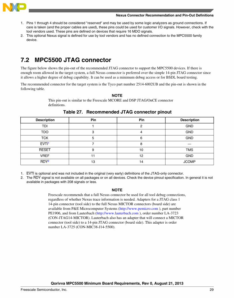
7.2 MPC5500 JTAG connectorThe figure below shows the pin-out of the recommended JTAG connector to support the MPC5500 devices. If there isenough room allowed in the target system, a full Nexus connector is preferred over the simple 14-pin JTAG connector sinceit allows a higher degree of debug capability. It can be used as a minimum debug access or for BSDL board testing.
The recommended connector for the target system is the Tyco part number 2514-6002UB and the pin-out is shown in thefollowing table.
NOTEThis pin-out is similar to the Freescale MCORE and DSP JTAG/OnCE connectordefinitions.
Table 27. Recommended JTAG connector pinout
Description Pin Pin Description
TDI 1 2 GND
TDO 3 4 GND
TCK 5 6 GND
EVTI1 7 8 —
RESET 9 10 TMS
VREF 11 12 GND
RDY2 13 14 JCOMP
1. EVTI is optional and was not included in the original (very early) definitions of the JTAG-only connector.2. The RDY signal is not available on all packages or on all devices. Check the device pinout specification. In general it is not
available in packages with 208 signals or less.
NOTEFreescale recommends that a full Nexus connector be used for all tool debug connections,regardless of whether Nexus trace information is needed. Adapters for a JTAG class 114-pin connector (tool side) to the full Nexus MICTOR connectors (board side) areavailable from P&E Microcomputer Systems (http://www.pemicro.com ), part numberPE1906, and from Lauterbach (http://www.lauterbach.com ), order number LA-3723(CON-JTAG14-MICTOR). Lauterbach also has an adapter that will connect a MICTORconnector (tool side) to a 14-pin JTAG connector (board side). This adapter is ordernumber LA-3725 (CON-MIC38-J14-5500).
Nexus Connector Recommendation and Pin-Out Definitions
Qorivva MPC5500 Minimum Board Requirements, Rev 0, August 21, 2013
Freescale Semiconductor, Inc. 29
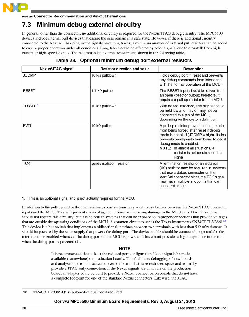
7.3 Minimum debug external circuitryIn general, other than the connector, no additional circuitry is required for the Nexus/JTAG debug circuitry. The MPC5500devices include internal pull devices that ensure the pins remain in a safe state. However, if there is additional circuitryconnected to the Nexus/JTAG pins, or the signals have long traces, a minimum number of external pull resistors can be addedto ensure proper operation under all conditions. Long traces could be affected by other signals, due to crosstalk from high-current or high-speed signals. The recommended external resistors are shown in the following table.
Table 28. Optional minimum debug port external resistors
Nexus/JTAG signal Resistor direction and value Description
JCOMP 10 kΩ pulldown Holds debug port in reset and preventsany debug commands from interferingwith the normal operation of the MCU.
RESET 4.7 kΩ pullup The RESET input should be driven froman open collector output; therefore, itrequires a pull-up resistor for the MCU.
TD/WDT1 10 kΩ pulldown With no tool attached, this signal shouldbe held low and may or may not beconnected to a pin of the MCU,depending on the system definition.
EVTI 10 kΩ pullup A pull-up resistor prevents debug modefrom being forced after reset if debugmode is enabled (JCOMP = high). It alsoprevents breakpoints from being forced ifdebug mode is enabled.NOTE: In almost all situations, a
resistor is not required on thissignal.
TCK series isolation resistor A termination resistor or an isolation(0Ω) resistor may be required in systemsthat use a debug connector on theVertiCal connector since the TCK signalmay have multiple endpoints that cancause reflections.
1. This is an optional signal and is not actually required for the MCU.
In addition to the pull-up and pull-down resistors, some systems may want to use buffers between the Nexus/JTAG connectorinputs and the MCU. This will prevent over-voltage conditions from causing damage to the MCU pins. Normal systemsshould not require this circuitry, but it is helpful in systems that can be exposed to improper connections that provide voltagesthat are outside the operating conditions of the MCU. A common circuit to use is the Texas Instruments SN74CBTLV386112.This device is a bus switch that implements a bidirectional interface between two terminals with less than 5 Ω of resistance. Itshould be powered by the same supply that powers the debug port. The device enable should be connected to ground for theinterface to be enabled whenever the debug port on the MCU is powered. This circuit provides a high impedance to the toolwhen the debug port is powered off.
NOTEIt is recommended that at least the reduced port configuration Nexus signals be madeavailable (somewhere) on production boards. This facilitates debugging of new boardsand analysis of errors in software, even on boards that have restricted space and normallyprovide a JTAG-only connection. If the Nexus signals are available on the productionboard, an adapter could be built to provide a Nexus connection on boards that do not havea complete footprint for one of the standard Nexus connectors. Likewise, the JTAG
12. SN74CBTLV3861-Q1 is automotive qualified if required.
Nexus Connector Recommendation and Pin-Out Definitions
Qorivva MPC5500 Minimum Board Requirements, Rev 0, August 21, 2013
30 Freescale Semiconductor, Inc.
connector does not have to be populated on production boards and could even utilize asmaller connector footprint that could be used with an adapter to the standard debugconnections.
In systems that use a VertiCal mounted debug connector and have a JTAG connector/footprint in the target system,termination may be required on the JTAG Test Clock (TCK) to avoid ringing due to the multiple signal endpoints.
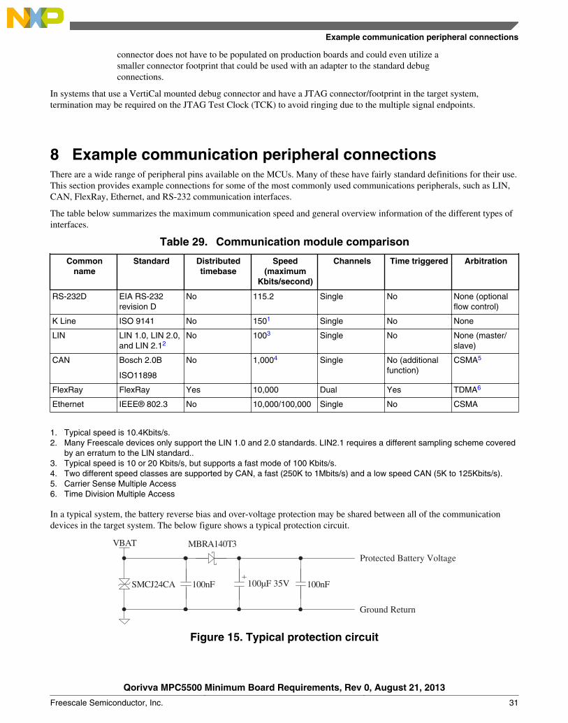
8 Example communication peripheral connectionsThere are a wide range of peripheral pins available on the MCUs. Many of these have fairly standard definitions for their use.This section provides example connections for some of the most commonly used communications peripherals, such as LIN,CAN, FlexRay, Ethernet, and RS-232 communication interfaces.
The table below summarizes the maximum communication speed and general overview information of the different types ofinterfaces.
Table 29. Communication module comparison
Commonname
Standard Distributedtimebase
Speed(maximum
Kbits/second)
Channels Time triggered Arbitration
RS-232D EIA RS-232revision D
No 115.2 Single No None (optionalflow control)
K Line ISO 9141 No 1501 Single No None
LIN LIN 1.0, LIN 2.0,and LIN 2.12
No 1003 Single No None (master/slave)
CAN Bosch 2.0B
ISO11898
No 1,0004 Single No (additionalfunction)
CSMA5
FlexRay FlexRay Yes 10,000 Dual Yes TDMA6
Ethernet IEEE® 802.3 No 10,000/100,000 Single No CSMA
1. Typical speed is 10.4Kbits/s.2. Many Freescale devices only support the LIN 1.0 and 2.0 standards. LIN2.1 requires a different sampling scheme covered
by an erratum to the LIN standard..3. Typical speed is 10 or 20 Kbits/s, but supports a fast mode of 100 Kbits/s.4. Two different speed classes are supported by CAN, a fast (250K to 1Mbits/s) and a low speed CAN (5K to 125Kbits/s).5. Carrier Sense Multiple Access6. Time Division Multiple Access
In a typical system, the battery reverse bias and over-voltage protection may be shared between all of the communicationdevices in the target system. The below figure shows a typical protection circuit.
SMCJ24CA 100nF
VBAT
Protected Battery Voltage
100nF
MBRA140T3
100μF 35V
Ground Return
Figure 15. Typical protection circuit
Example communication peripheral connections
Qorivva MPC5500 Minimum Board Requirements, Rev 0, August 21, 2013
Freescale Semiconductor, Inc. 31
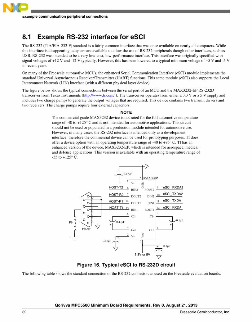
8.1 Example RS-232 interface for eSCIThe RS-232 (TIA/EIA-232-F) standard is a fairly common interface that was once available on nearly all computers. Whilethis interface is disappearing, adapters are available to allow the use of RS-232 peripherals though other interfaces, such asUSB. RS-232 was intended to be a very low-cost, low-performance interface. This interface was originally specified withsignal voltages of +12 V and -12 V typically. However, this has been lowered to a typical minimum voltage of +5 V and -5 Vin recent years.
On many of the Freescale automotive MCUs, the enhanced Serial Communication Interface (eSCI) module implements thestandard Universal Asynchronous Receiver/Transmitter (UART) functions. This same module (eSCI) also supports the LocalInterconnect Network (LIN) interface (with a different physical layer device).
The figure below shows the typical connections between the serial port of an MCU and the MAX3232-EP RS-232Dtransceiver from Texas Instruments (http://www.ti.com/ ). The transceiver operates from either a 3.3 V or a 5 V supply andincludes two charge pumps to generate the output voltages that are required. This device contains two transmit drivers andtwo receivers. The charge pumps require four external capacitors.
NOTEThe commercial grade MAX3232 device is not rated for the full automotive temperaturerange of -40 to +125° C and is not intended for automotive applications. This circuitshould not be used or populated in a production module intended for automotive use.However, in many cases, the RS-232 interface is intended only as a developmentinterface; therefore the commercial device can be used for prototyping purposes. TI doesoffer a device option with an operating temperature range of -40 to +85° C. TI has anenhanced version of the device, MAX3232-EP, which is intended for aerospace, medical,and defense applications. This version is available with an operating temperature range of-55 to +125° C.
+ 0.47μF +
0.1μF
3.3V or 5V
162738495
DB-9F
FB
1
V+
C1-
C2+
C2-
V-
DOUT2
8
Vcc
16
GN
D 15
DOUT1
RIN1 ROUT1
DIN1
DIN2
ROUT2
0.1μF
eSCI_TXDA
eSCI_RXDA
MAX3232
eSCI_RXDA2
HOST-R2 eSCI_TXDA2
HOST-T2 9
HOST-R1
HOST-T1
+
0.47μF
+
0.47μF
+
10
11
12
7
RIN2
14
13
2
4C1+
3
6
5
Figure 16. Typical eSCI to RS-232D circuit
The following table shows the standard connection of the RS-232 connector, as used on the Freescale evaluation boards.
Example communication peripheral connections
Qorivva MPC5500 Minimum Board Requirements, Rev 0, August 21, 2013
32 Freescale Semiconductor, Inc.
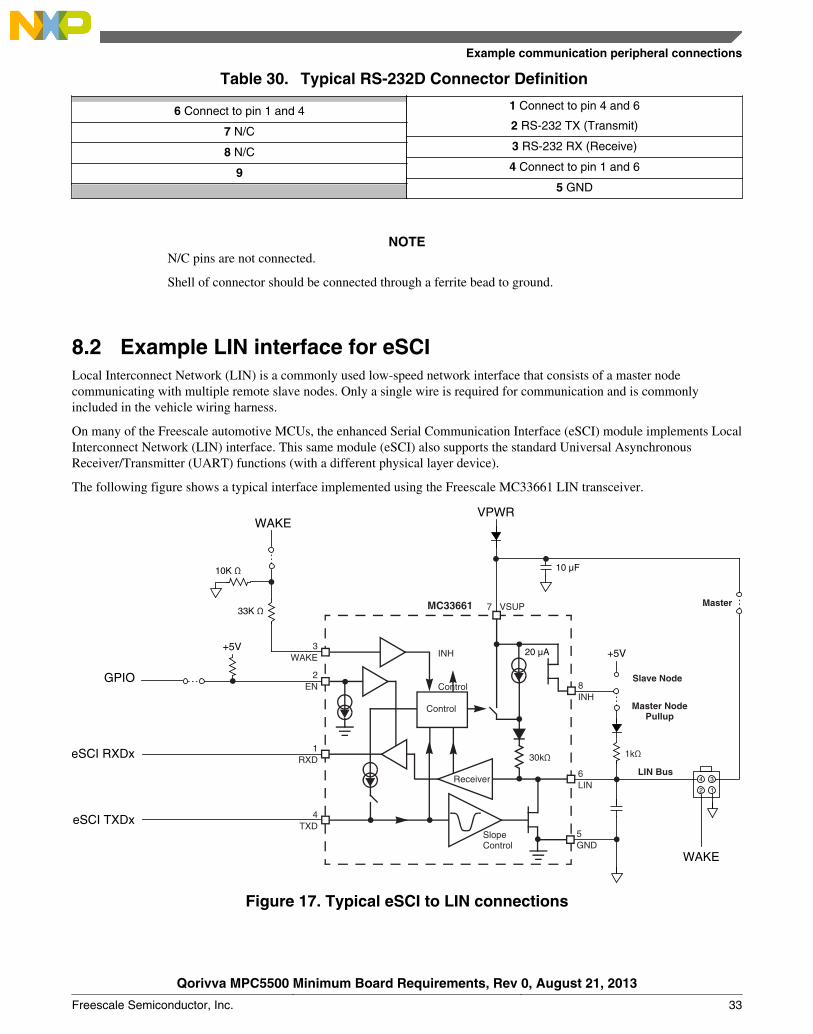
Table 30. Typical RS-232D Connector Definition
1 Connect to pin 4 and 66 Connect to pin 1 and 42 RS-232 TX (Transmit)7 N/C3 RS-232 RX (Receive)8 N/C4 Connect to pin 1 and 69
5 GND
NOTEN/C pins are not connected.
Shell of connector should be connected through a ferrite bead to ground.
8.2 Example LIN interface for eSCILocal Interconnect Network (LIN) is a commonly used low-speed network interface that consists of a master nodecommunicating with multiple remote slave nodes. Only a single wire is required for communication and is commonlyincluded in the vehicle wiring harness.
On many of the Freescale automotive MCUs, the enhanced Serial Communication Interface (eSCI) module implements LocalInterconnect Network (LIN) interface. This same module (eSCI) also supports the standard Universal AsynchronousReceiver/Transmitter (UART) functions (with a different physical layer device).
The following figure shows a typical interface implemented using the Freescale MC33661 LIN transceiver.
Control
Receiver
INH
Control
5 GND
7 VSUPMC33661
LIN Bus
Master Node Pullup
eSCI RXDx
eSCI TXDx
VPWR
33K Ω
+5V
10K Ω
GPIO
+5V
Slave Node
12
34
WAKE
WAKE
Master
3 WAKE
2 EN
1 RXD
4 TXD
6 LIN
8 INH
30kΩ
Slope Control
20 μA
10 μF
1kΩ
Figure 17. Typical eSCI to LIN connections
Example communication peripheral connections
Qorivva MPC5500 Minimum Board Requirements, Rev 0, August 21, 2013
Freescale Semiconductor, Inc. 33
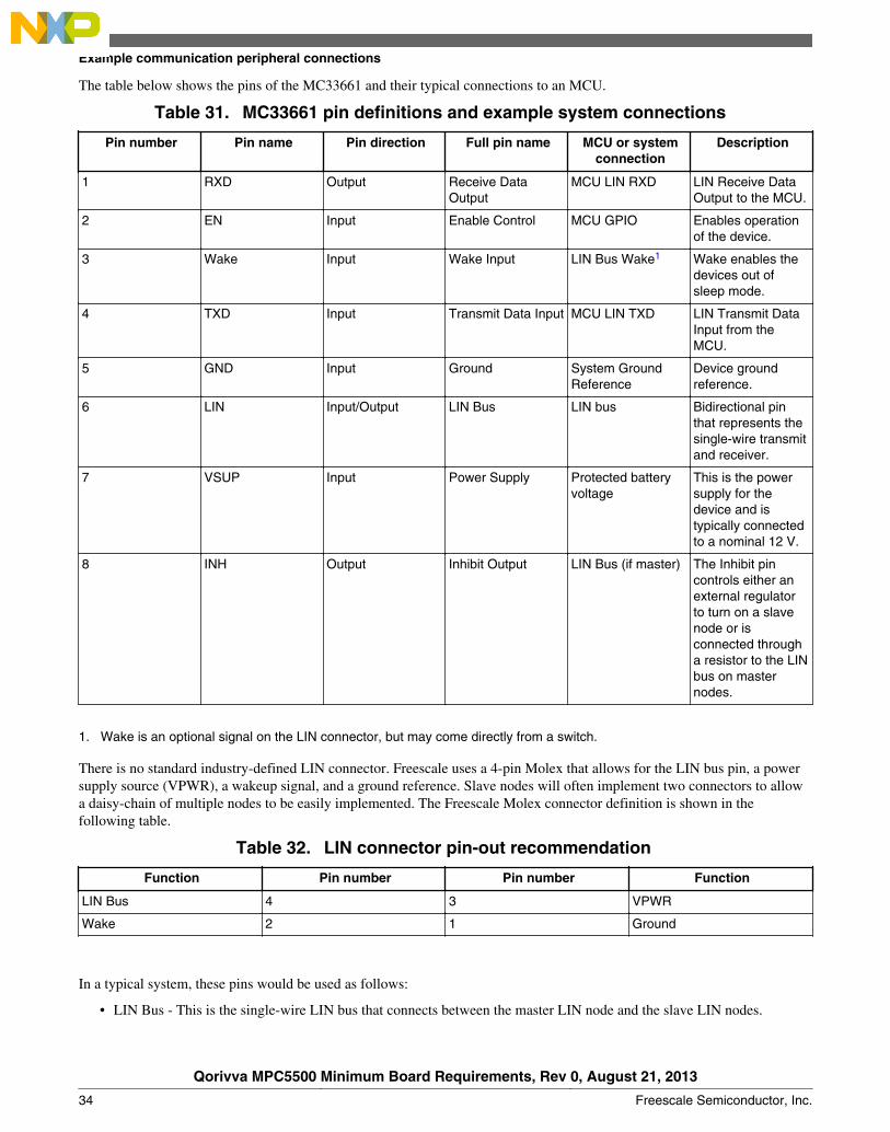
The table below shows the pins of the MC33661 and their typical connections to an MCU.
Table 31. MC33661 pin definitions and example system connections
Pin number Pin name Pin direction Full pin name MCU or systemconnection
Description
1 RXD Output Receive DataOutput
MCU LIN RXD LIN Receive DataOutput to the MCU.
2 EN Input Enable Control MCU GPIO Enables operationof the device.
3 Wake Input Wake Input LIN Bus Wake1 Wake enables thedevices out ofsleep mode.
4 TXD Input Transmit Data Input MCU LIN TXD LIN Transmit DataInput from theMCU.
5 GND Input Ground System GroundReference
Device groundreference.
6 LIN Input/Output LIN Bus LIN bus Bidirectional pinthat represents thesingle-wire transmitand receiver.
7 VSUP Input Power Supply Protected batteryvoltage
This is the powersupply for thedevice and istypically connectedto a nominal 12 V.
8 INH Output Inhibit Output LIN Bus (if master) The Inhibit pincontrols either anexternal regulatorto turn on a slavenode or isconnected througha resistor to the LINbus on masternodes.
1. Wake is an optional signal on the LIN connector, but may come directly from a switch.
There is no standard industry-defined LIN connector. Freescale uses a 4-pin Molex that allows for the LIN bus pin, a powersupply source (VPWR), a wakeup signal, and a ground reference. Slave nodes will often implement two connectors to allowa daisy-chain of multiple nodes to be easily implemented. The Freescale Molex connector definition is shown in thefollowing table.
Table 32. LIN connector pin-out recommendation
Function Pin number Pin number Function
LIN Bus 4 3 VPWR
Wake 2 1 Ground
In a typical system, these pins would be used as follows:
• LIN Bus - This is the single-wire LIN bus that connects between the master LIN node and the slave LIN nodes.
Example communication peripheral connections
Qorivva MPC5500 Minimum Board Requirements, Rev 0, August 21, 2013
34 Freescale Semiconductor, Inc.
• VPWR - This connector input can be used as the power input to a slave node. Care should be taken that sufficientcurrent is available for the total number of LIN slaves that are powered through this connection. In some systems, thismay come from the master LIN node.
• Wake - The Wake signal is typically used for each individual slave node to enable the LIN physical interface of thatnode and consequently enable the power supply (using the INH output) to power up the MCU to perform some action.For example, when the handle on a car door is lifted, turn on the MCU that controls a function inside the vehicle, suchas power a smart dome light or enable the controls of a smart seat.
• Ground - Ground reference for the module.
Part numbers for the 4-pin Molex Mini-Fit Jr.™ connector are shown in the table below.
Table 33. Recommended 4-pin Molex Mini-Fit Jr.™ connector part numbers
Description Manufacturer part number (Molex)
4-pin right-angle connector with flange for target system, tincontacts, with latch
39-29-1048
4-pin right-angle connector with pegs for target system, tincontacts, with latch
39-30-1040
4-pin vertical connector with pegs for target system, tincontacts, with latch
39-29-9042
4-pin right-angle connector with flange for target system, goldcontacts, latch
39-29-5043
Mating connector with latch for cable assemblies 39-01-2040
Female terminal for mating cable assembly 39-00-0077
8.3 CAN interface circuitryController Area Network (CAN) is commonly used in almost all automotive applications to allow communication betweenvarious microchips in the car.
The number of CAN modules on-chip varies from device to device. A separate CAN transceiver is required for each CANmodule, although some CAN transceivers may have more than one transceiver on a single chip. It is possible to connect twoCAN modules to a single transceiver if the transmit pins are put into open-collector mode with an external pullup resistor.However, the value of this resistor may limit the maximum speed of the CAN module if not sized properly for the speed.
Freescale CAN modules conform to CAN protocol specification version 2.0B, and the transceivers shown in this applicationnote comply with ISO 11898 physical layer standard.
Typically, CAN is used at either a low speed (5 kbit/s to 125 kbit/s) or a high speed (250 kbit/s to 1 Mbit/s). Powertrainapplications typically use a high speed (HS) CAN interface to communicate between the engine control unit and thetransmission control unit. Body and chassis applications typically use a low speed (LS) CAN interface. In the dashboard of avehicle, there is typically a gateway device that interfaces between HS and LS CAN networks.
Example communication peripheral connections
Qorivva MPC5500 Minimum Board Requirements, Rev 0, August 21, 2013
Freescale Semiconductor, Inc. 35
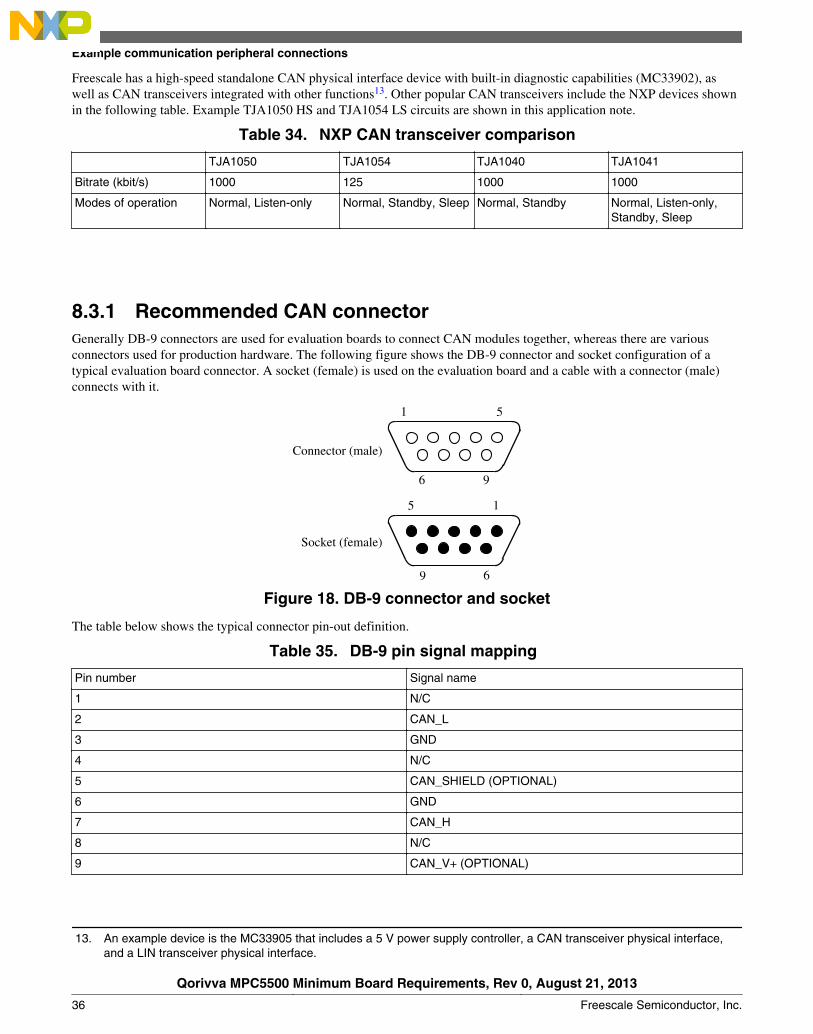
Freescale has a high-speed standalone CAN physical interface device with built-in diagnostic capabilities (MC33902), aswell as CAN transceivers integrated with other functions13. Other popular CAN transceivers include the NXP devices shownin the following table. Example TJA1050 HS and TJA1054 LS circuits are shown in this application note.
Table 34. NXP CAN transceiver comparison
TJA1050 TJA1054 TJA1040 TJA1041
Bitrate (kbit/s) 1000 125 1000 1000
Modes of operation Normal, Listen-only Normal, Standby, Sleep Normal, Standby Normal, Listen-only,Standby, Sleep
8.3.1 Recommended CAN connectorGenerally DB-9 connectors are used for evaluation boards to connect CAN modules together, whereas there are variousconnectors used for production hardware. The following figure shows the DB-9 connector and socket configuration of atypical evaluation board connector. A socket (female) is used on the evaluation board and a cable with a connector (male)connects with it.
1 5
6 9
Connector (male)
15
69
Socket (female)
Figure 18. DB-9 connector and socket
The table below shows the typical connector pin-out definition.
Table 35. DB-9 pin signal mapping
Pin number Signal name
1 N/C
2 CAN_L
3 GND
4 N/C
5 CAN_SHIELD (OPTIONAL)
6 GND
7 CAN_H
8 N/C
9 CAN_V+ (OPTIONAL)
13. An example device is the MC33905 that includes a 5 V power supply controller, a CAN transceiver physical interface,and a LIN transceiver physical interface.
Example communication peripheral connections
Qorivva MPC5500 Minimum Board Requirements, Rev 0, August 21, 2013
36 Freescale Semiconductor, Inc.
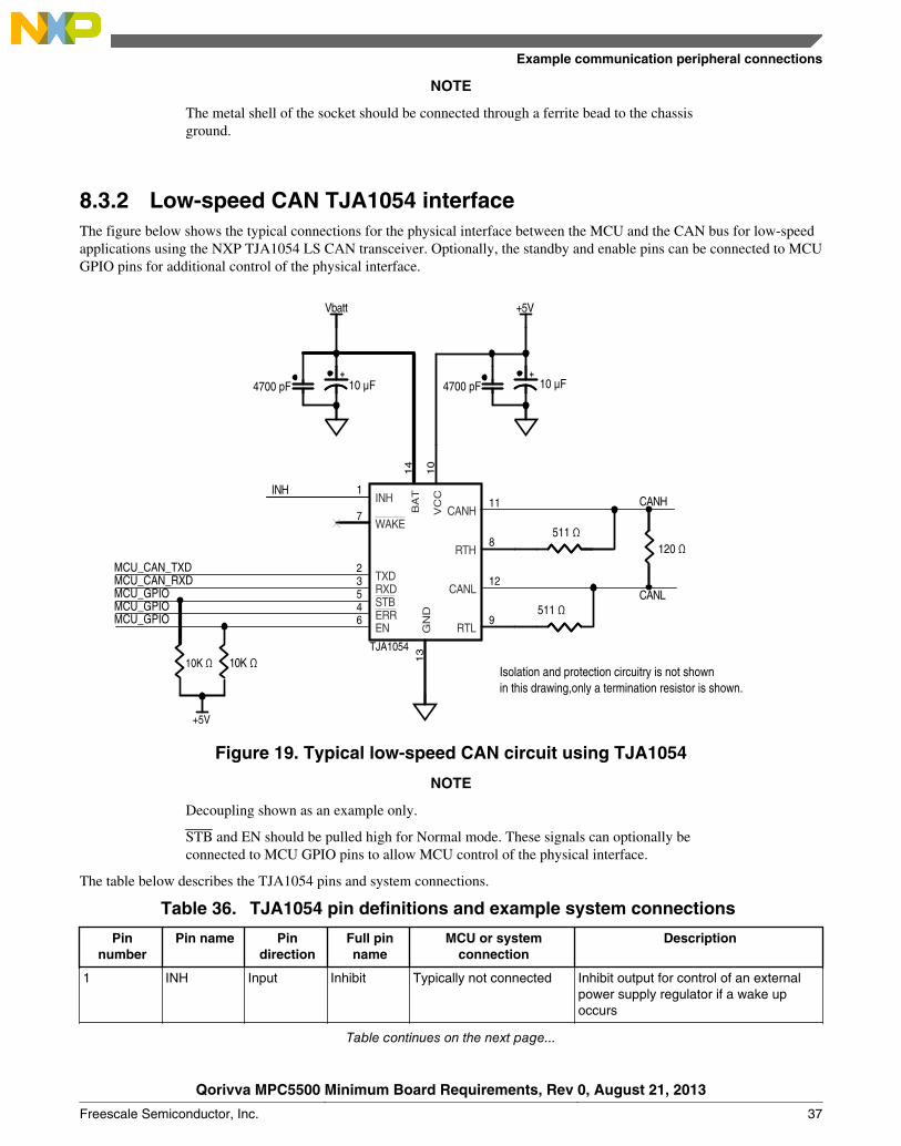
NOTE
The metal shell of the socket should be connected through a ferrite bead to the chassisground.
8.3.2 Low-speed CAN TJA1054 interfaceThe figure below shows the typical connections for the physical interface between the MCU and the CAN bus for low-speedapplications using the NXP TJA1054 LS CAN transceiver. Optionally, the standby and enable pins can be connected to MCUGPIO pins for additional control of the physical interface.
MCU_CAN_TXDMCU_CAN_RXD
MCU_GPIO
INHCANH
CANL
Vbatt +5V
+5V
10K Ω
10K ΩTJA1054
INH 1
WAKE7
STB5
EN 6
TXD 2
ERR4
RXD 3
GN
D
13
RTL 9
CANH 11
CANL 12
RTH 8
BA
T
14
VC
C
10
4700 pF++
10 μF
4700 pF++
10 μF
511 Ω120 Ω
511 ΩMCU_GPIO
MCU_GPIO
Isolation and protection circuitry is not shown in this drawing,only a termination resistor is shown.
Figure 19. Typical low-speed CAN circuit using TJA1054
NOTE
Decoupling shown as an example only.
STB and EN should be pulled high for Normal mode. These signals can optionally beconnected to MCU GPIO pins to allow MCU control of the physical interface.
The table below describes the TJA1054 pins and system connections.
Table 36. TJA1054 pin definitions and example system connections
Pinnumber
Pin name Pindirection
Full pinname
MCU or systemconnection
Description
1 INH Input Inhibit Typically not connected Inhibit output for control of an externalpower supply regulator if a wake upoccurs
Table continues on the next page...
Example communication peripheral connections
Qorivva MPC5500 Minimum Board Requirements, Rev 0, August 21, 2013
Freescale Semiconductor, Inc. 37
Table 36. TJA1054 pin definitions and example system connections (continued)
Pinnumber
Pin name Pindirection
Full pinname
MCU or systemconnection
Description
2 TXD Input TransmitData
MCU CAN TXD CAN transmit data input from the MCU
3 RXD Output ReceiveData
MCU CAN RXD CAN receive data output to the MCU
4 ERR Output Error MCU GPIO The error signal indicates a bus failure innormal operating mode or a wake-up isdetected in Standby or Sleep modes.
5 STB Input VoltageSupply forIO
MCU GPIO Standby input for device. It is also usedin conjunction with the EN pin todetermine the mode of the transceiver.
6 EN Input Enable MCU GPIO Enable input for the device. It is alsoused in conjunction with the STB pin todetermine the mode of the transceiver.
7 WAKE Input Wake Typically not connected Wake input (active low), both falling andrising edges are detected
8 RTH Input TerminationResistorHigh
Resistor to CANH Termination resistor for the CAN bushigh
9 RTL Input TerminationResistorLow
Resistor to CANL Termination resistor for the CAN buslow
1
10 VCC Input VoltageSupply
5 V Digital IO supply voltage, 5 V
11 CANH Output CAN BusHigh
CAN Bus Connector CAN bus high pin
12 CANL Input/Output CAN BusLow
CAN Bus Connector CAN bus low pin
13 Ground Output Ground Ground Ground return termination path
14 BAT Input Standby Battery voltage Battery supply pin, nominally 12 V
1. This allows the transceiver to control the CAN bus impedance under an error condition.
8.3.3 High-speed CAN TJA1050 interfaceThe figure below below shows the typical connections for the physical interface between the MCU and the CAN bus forhigh-speed applications using the NXP TJA1050 HS CAN transceiver.
Example communication peripheral connections
Qorivva MPC5500 Minimum Board Requirements, Rev 0, August 21, 2013
38 Freescale Semiconductor, Inc.
MCU_CAN_TXD
VREF
MCU_CAN_RXD
CANH
CANL
+5V
60 Ω
60 Ω
60 Ω
60 Ω
10K
4700 pF
U1
TJA1050T
U1
TJA1050T
GND 2
VCC 3
CANH 7
CANL 6
S 8
TXD 1
RXD 4
VREF 5
4700 pF
4700 pF
++ 10 μF
Figure 20. Typical high-speed CAN circuit using TJA1050
NOTE
Decoupling shown as an example only.
TXD/RXD pullup/pulldown may be required, depending on device implementation.
The table below as describes the TJA1050 pin and system connections.
Table 37. TJA1050 pin definitions and example system connections
Pinnumber
Pin name Pindirection
Full pinname
MCU or systemconnection
Description
1 TXD Input TransmitData
MCU CAN TXD CAN transmit data input from the MCU
2 GND Output Ground Ground Ground return termination
3 VCC Input — 5 V Voltage supply input (5 V)
4 RXD Output ReceiveData
MCU CAN RXD CAN receive data output to the MCU
5 VREF Output ReferencevoltageOutput
Not used Mid-supply output voltage. This istypically not used in many systems, butcan be used if voltage translation needsto be done between the CAN transceiverand the MCU.
6 CANL Input/Output CAN BusLow
CAN Bus Connector CAN bus low pin
7 CANH Input/Output CAN BusHigh
CAN Bus Connector CAN bus high pin
8 S Input Select Grounded or MCU GPIO Select for high-speed mode or silentmode. Silent mode disables thetransmitter, but keeps the rest of thedevice active. This may be used in thecase of an error condition.
Example communication peripheral connections
Qorivva MPC5500 Minimum Board Requirements, Rev 0, August 21, 2013
Freescale Semiconductor, Inc. 39
8.3.4 High-speed CAN with diagnostics: MC33902 interfaceFor target systems that require full diagnostics of the CAN interface, the Freescale MC33902 high-speed CAN transceiver isavailable. Features of this device are:
• High-speed CAN interface for baud rates of 40 kbit/s to 1.0 Mbit/s• Compatible with ISO 11898 standard• Single supply from battery; no need for a 5.0 V supply for CAN interface• I/O compatible from 2.75 V to 5.5 V via a dedicated input terminal (3.3 V or 5.0 V logic compatible)• Low-power mode with remote CAN wakeup and local wake-up recognition and reporting• CAN bus failure diagnostics and TXD/RXD pin monitoring, cold start detection, and wake-up sources reported through
the ERR pin• Enhanced diagnostics for bus, TXD, RXD, and supply pins available through pseudo-SPI via existing terminals EN,
STBY, and ERR• Split terminal for bus recessive level stabilization• INH output to control external voltage regulator
A block diagram of this transceiver is shown below.
Differential Receiver
Driver
Driver
2.5 V
Receiver
Pattern Detection
VSUP
CANH
CANL
QH
QL
Rin
Rin
INH
STBY
ERR
VSUP
Logi
c C
ontr
ol /
Inte
rfac
e / P
_SP
I
VIO
5.0 V Regulator
VDD
Failure Detection Buffer
VDD
SPLIT
Monitoring
INH
Wake-up
& Management
WAKE
GND
Detector
control
TXD
RXD
EN
Vio
Thermal
Figure 21. MC33902 block diagram
While a full SPI interface is not available for the diagnostic information, a quasi-SPI interface is available to communicate tothe MCU. This interface is referred to as the P_SPI interface in the MC33902 data sheet.
The figure below shows an example schematic using the MC33902.
Example communication peripheral connections
Qorivva MPC5500 Minimum Board Requirements, Rev 0, August 21, 2013
40 Freescale Semiconductor, Inc.
INH
MCU_GPIO or SPI_TXD
MCU_CAN_TX
MCU_CAN_RX CANL
CANH
+5V Vbatt
+5V
220 pF
4700 pF
10KΩ
4700 pF
++ 10 μF
10KΩ P
ES
D24
VL1
BA
PE
SD
24V
L1B
AP
ES
D24
VL1
BA
PE
SD
24V
L1B
A
30Ω
220 pF
4700 pF
30Ω
++ 10 μF
22μH
21
4 3
MC33902
SPLIT 11
CANH 13
CANL 12
STBY 14
WAKE 9
EN 6
VIO 5
INH 7
TXD 1
RXD 4
NERR 8
Vd
d
3
Vsu
p
10
GND 2
MCU_GPIO or SPI_CLKMCU_GPIO or SPI_RXD
Figure 22. Typical high-speed CAN circuit using the MC33902
NOTE
Decoupling shown as an example only.
Bus protection is shown as an example only.
The table below shows the pins of the MC33902 and the possible connections to a MCU and the target system.
Table 38. MC33902 pin definitions and example system connections
Pinnumber
Pin name Pindirection
Full pinname
MCU or systemconnection
Description
1 TXD Input TransmitData
MCU CAN TXD CAN transmit data input from the MCU
2 GND Output Ground Ground Ground termination
3 VDD Output VDDInternalRegulatorOutput
Bypass capacitors only 5 V power supply output. Requiresexternal bypass capacitors.
4 RXD Output ReceiveData
MCU CAN TXD CAN receive data output to the MCU
5 VIO Input VoltageSupply forIO
3.3 V or 5 V Supply voltage input for the digital inputand output pins. This should be matchedto the IO voltage supply of the MCU.Most typically, this is 5 V, but could alsobe 3.3 V.
Table continues on the next page...
Example communication peripheral connections
Qorivva MPC5500 Minimum Board Requirements, Rev 0, August 21, 2013
Freescale Semiconductor, Inc. 41
Table 38. MC33902 pin definitions and example system connections (continued)
Pinnumber
Pin name Pindirection
Full pinname
MCU or systemconnection
Description
6 EN Input Enable MCU GPIO or SPItransmit data output
This is the enable input for the device instatic mode control. This is the masteroutput/slave input when used in SPImode, and the MOSI (master out, slavein) during SPI operation.
7 INH Output Inhibit Use depends on intendedoperation (see text below)
Inhibit output for control of an externalpower supply regulator
8 ERR Output Active LowError
MCU GPIO or SPI receivedata input
Pin for static error and wakeup flagreporting MISO (master in, slave out)during SPI operation
9 WAKE Input Wake MCU GPIO (output) Wake input
10 VSUP Input VoltageSupply
Battery voltage Battery supply pin, nominally 12 V
11 SPLIT Output Split CAN termination midpoint Output for connection of the CAN bustermination middle point
12 CANL Input/output CAN BusLow
CAN Bus Connector CAN bus low pin
13 CANH Input/output CAN BusHigh
CAN Bus Connector CAN bus high pin
14 NTSB Input Standby MCU GPIO or SPI Clockoutput
Standby input for device static modecontrol. CLK (Clock) during P_SPIoperation
The use of the Inhibit pin (INH) is dependent on the selected target system operation. INH can turn an external power supplyon and therefore wake a connected MCU for operation to save power when MCU operation is not required. In MPC5500 andMPC5600 automotive power train applications (engine control), INH is typically not used. However, in automotive body andchassis applications, it may be used.
8.4 FlexRay interface circuitry using TJA1080AFlexRay is an automotive fault-tolerant 2-wire communications interface. FlexRay is generally used at 10,000 kbits/s (10Mbit/s).
Freescale FlexRay devices implement a bus driver interface compliant with Communications System Electrical PhysicalLayer Specification, Version 2.1 Rev A.
Typically, FlexRay bus data rates of 10 Mbit/s, 8 Mbit/s, 5 Mbit/s, and 2.5 Mbit/s are supported and although the logicportions of the interface are implemented in the device, an external physical interface device is required to allow multipleFlexRay modules to be connected together.
The NXP™ (http://www.nxp.com ) TJA1080A device is typically used as the FlexRay transceiver, although others areavailable. One transceiver is required for each FlexRay channel. The figure below shows the typical connections using theTJA1080A.
Example communication peripheral connections
Qorivva MPC5500 Minimum Board Requirements, Rev 0, August 21, 2013
42 Freescale Semiconductor, Inc.
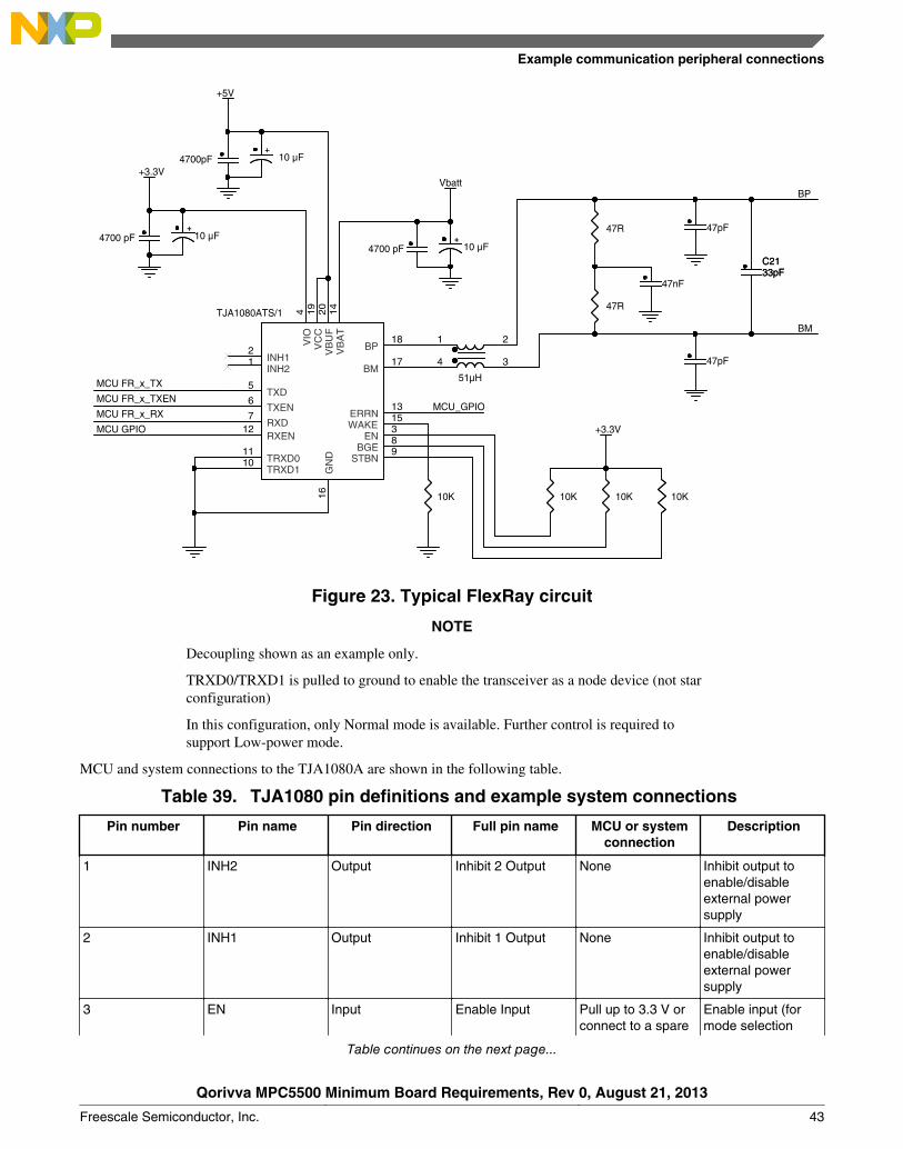
MCU FR_x_TX
MCU FR_x_TXEN
MCU FR_x_RX
MCU GPIO
MCU_GPIO
BP
BM
Vbatt
+5V
+3.3V
+3.3V
+10 μF
+
10K
47R
47nF
4700 pF
10K
C21 33pFC21 33pF
+10 μF
+
4700pF
47R
++10 μF
47pF
TJA1080ATS/1
TRXD0 11
TRXD1 10
TXD 5
TXEN 6
BGE 8
STBN 9
EN 3WAKE 15
INH2 1 INH1 2 BP
18
BM 17
RXD 7 ERRN
13
RXEN 12
VIO
4
VC
C
19
VB
UF
20
VB
AT
14
GN
D
16
47pF
10K
4700 pF
51μH
21
4 3
10K
Figure 23. Typical FlexRay circuit
NOTE
Decoupling shown as an example only.
TRXD0/TRXD1 is pulled to ground to enable the transceiver as a node device (not starconfiguration)
In this configuration, only Normal mode is available. Further control is required tosupport Low-power mode.
MCU and system connections to the TJA1080A are shown in the following table.
Table 39. TJA1080 pin definitions and example system connections
Pin number Pin name Pin direction Full pin name MCU or systemconnection
Description
1 INH2 Output Inhibit 2 Output None Inhibit output toenable/disableexternal powersupply
2 INH1 Output Inhibit 1 Output None Inhibit output toenable/disableexternal powersupply
3 EN Input Enable Input Pull up to 3.3 V orconnect to a spare
Enable input (formode selection
Table continues on the next page...
Example communication peripheral connections
Qorivva MPC5500 Minimum Board Requirements, Rev 0, August 21, 2013
Freescale Semiconductor, Inc. 43
Table 39. TJA1080 pin definitions and example system connections (continued)
Pin number Pin name Pin direction Full pin name MCU or systemconnection
Description
MCU GPIO (outputto MCU)
(along with theSTBN pin). Internalpulldown(transmitterdisabled, but allowsreception, listenonly mode)
4 VIO Input (power) IO Power Supply 3.3 V Power supply inputfor the MCU I/Osignals
5 TXD Input Transmit Data MCU FR_x_TX Transmit data fromthe MCU fortransmitting on theFlexRay bus.Internal pullup
6 TXEN Input Transmit Enable MCU FR_x_TXEN1
Transmit enable. Ahigh level disablesthe transmitter.Internal pullup
7 RXD Output Receive Data MCU FR_x_RX1
Receive data fromthe FlexRay bus tothe MCU
8 BGE Input Bus GuardianEnable
Pull up to 3.3 V The bus guardianinput disables thetransmitter. Thisfeature is currentlynot supported
9 STBN Input Standby Input Pull up to 3.3 V orconnect to a spareMCU GPIO
Standby modeenable input (low toenter low powermode). Internalpulldown
10 TRXD1 Input/Output Data Bus Line 1 Tie low Data bus signal 1for an inner starconnection
11 TRXD0 Input/Output Data Bus Line 0 Tie low Data bus signal 0for an inner starconnection
12 RXEN Output Receive Enable MCU GPIO (inputto MCU)
Receive dataenable indicatesdata is availablefrom the bus (lowduring activity)
13 ERRN Output Error Output MCU GPIO (inputto MCU)
The errordiagnostic outputdrives low upon anerror
14 VBAT Input (power) Battery SupplyVoltage
Protected batteryvoltage
Battery supplyvoltage
Table continues on the next page...
Example communication peripheral connections
Qorivva MPC5500 Minimum Board Requirements, Rev 0, August 21, 2013
44 Freescale Semiconductor, Inc.
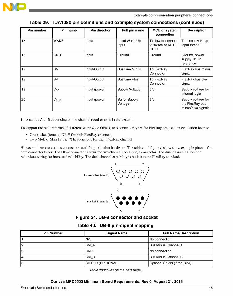
Table 39. TJA1080 pin definitions and example system connections (continued)
Pin number Pin name Pin direction Full pin name MCU or systemconnection
Description
15 WAKE Input Local Wake UpInput
Tie low or connectto switch or MCUGPIO
The local wakeupinput forces
16 GND Input Ground Ground Ground, powersupply returnreference
17 BM Input/Output Bus Line Minus To FlexRayConnector
FlexRay bus minussignal
18 BP Input/Output Bus Line Plus To FlexRayConnector
FlexRay bus plussignal
19 VCC Input (power) Supply Voltage 5 V Supply voltage forinternal logic
20 VBUF Input (power) Buffer SupplyVoltage
5 V Supply voltage forthe FlexRay busminus/plus signals
1. x can be A or B depending on the channel requirements in the system.
To support the requirements of different worldwide OEMs, two connector types for FlexRay are used on evaluation boards:
• One socket (female) DB-9 for both FlexRay channels• Two Molex (Mini Fit Jr.™) headers, one for each FlexRay channel
However, there are various connectors used for production hardware. The tables and figures below show example pinouts forboth connector types. The DB-9 connector allows for two channels on a single connector. The dual channels allow forredundant wiring for increased reliability. The dual channel capability is built into the FlexRay standard.
1 5
6 9
Connector (male)
15
69
Socket (female)
Figure 24. DB-9 connector and socket
Table 40. DB-9 pin-signal mapping
Pin Number Signal Name Full Name/Description
1 N/C No connection
2 BM_A Bus Minus Channel A
3 GND No connection
4 BM_B Bus Minus Channel B
5 SHIELD (OPTIONAL) Optional Shield (if required)
Table continues on the next page...
Example communication peripheral connections
Qorivva MPC5500 Minimum Board Requirements, Rev 0, August 21, 2013
Freescale Semiconductor, Inc. 45

Table 40. DB-9 pin-signal mapping (continued)
Pin Number Signal Name Full Name/Description
6 N/C No connection
7 BP_A Bus Plus Channel A
8 BP_B Bus Plus Channel B
9 N/C No connection
NOTE
A socket (female) is used on the evaluation board and a cable with a connector (male)connects with this.
The metal shell of the socket should be connected through a ferrite bead to GND.
2
1
Latch Tab
Figure 25. Molex connector picture
Table 41. Molex pin-signal mapping
Pin Number Signal Name
1 BP
2 BM
NOTE
A connector (male) is used on the evaluation board and a cable with a socket (female)connects with this.
The Molex connectors are available in two types, one with pegs for mounting to the board and one without. The part numbersare shown in the following table.
Table 42. Recommended Molex Mini-Fit Jr. connector part numbers
Description Manufacturer Part Number (Molex)
2-pin vertical connector with pegs for target system, tincontacts, latch
39-29-9022
2-pin vertical connector without pegs for target system, tincontacts, latch
39-28-8020
Table continues on the next page...
Example communication peripheral connections
Qorivva MPC5500 Minimum Board Requirements, Rev 0, August 21, 2013
46 Freescale Semiconductor, Inc.
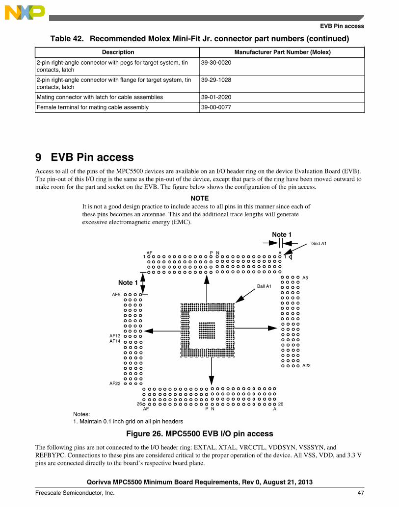
Table 42. Recommended Molex Mini-Fit Jr. connector part numbers (continued)
Description Manufacturer Part Number (Molex)
2-pin right-angle connector with pegs for target system, tincontacts, latch
39-30-0020
2-pin right-angle connector with flange for target system, tincontacts, latch
39-29-1028
Mating connector with latch for cable assemblies 39-01-2020
Female terminal for mating cable assembly 39-00-0077
9 EVB Pin accessAccess to all of the pins of the MPC5500 devices are available on an I/O header ring on the device Evaluation Board (EVB).The pin-out of this I/O ring is the same as the pin-out of the device, except that parts of the ring have been moved outward tomake room for the part and socket on the EVB. The figure below shows the configuration of the pin access.
NOTEIt is not a good design practice to include access to all pins in this manner since each ofthese pins becomes an antennae. This and the additional trace lengths will generateexcessive electromagnetic energy (EMC).
Note 1
Notes: 1. Maintain 0.1 inch grid on all pin headers
Note 1
1
26
A
A
AF NP
AF NP
1
26
AF13 AF14
A5
A22
AF5
AF22
Grid A1
Ball A1
Figure 26. MPC5500 EVB I/O pin access
The following pins are not connected to the I/O header ring: EXTAL, XTAL, VRCCTL, VDDSYN, VSSSYN, andREFBYPC. Connections to these pins are considered critical to the proper operation of the device. All VSS, VDD, and 3.3 Vpins are connected directly to the board’s respective board plane.
EVB Pin access
Qorivva MPC5500 Minimum Board Requirements, Rev 0, August 21, 2013
Freescale Semiconductor, Inc. 47
10 ReferencesMore information can be found in the documents shown in the table below.
Table 43. References
Document Number Document title Location
MPC5534RM MPC5534 Reference Manual www.freescale.com
MPC5553_MPC5554_RM MPC5553/5554 Reference Manual
MPC5561RM MPC5561 Reference Manual
MPC5565RM MPC5565 Reference Manual
MPC5566RM MPC5566 Reference Manual
MPC5567RM MPC5567 Reference Manual
MPC5534 MPC5534 Data Sheet
MPC5553 MPC5553 Data Sheet
MPC5554 MPC5554 Data Sheet
MPC5561 MPC5561 Data Sheet
MPC5565 MPC5565 Data Sheet
MPC5566 MPC5566 Data Sheet
MPC5567 MPC5567 Data Sheet
AN2614 Nexus Interface Connector Options forthe MPC5500 Family
AN2705 Signal Integrity Considerations withMPC5500-based Systems
AN2706 EMC Guidelines for MPC5500-basedSystems
References
Qorivva MPC5500 Minimum Board Requirements, Rev 0, August 21, 2013
48 Freescale Semiconductor, Inc.

How to Reach Us:
Home Page:freescale.com
Web Support:freescale.com/support
Information in this document is provided solely to enable system andsoftware implementers to use Freescale products. There are no expressor implied copyright licenses granted hereunder to design or fabricateany integrated circuits based on the information in this document.Freescale reserves the right to make changes without further notice toany products herein.
Freescale makes no warranty, representation, or guarantee regardingthe suitability of its products for any particular purpose, nor doesFreescale assume any liability arising out of the application or use ofany product or circuit, and specifically disclaims any and all liability,including without limitation consequential or incidental damages.“Typical” parameters that may be provided in Freescale data sheetsand/or specifications can and do vary in different applications, andactual performance may vary over time. All operating parameters,including “typicals,” must be validated for each customer application bycustomer's technical experts. Freescale does not convey any licenseunder its patent rights nor the rights of others. Freescale sells productspursuant to standard terms and conditions of sale, which can be foundat the following address: freescale.com/SalesTermsandConditions.
Freescale, the Freescale logo and Qorivva are trademarks of FreescaleSemiconductor, Inc., Reg. U.S. Pat. & Tm. Off. The Power Architectureand Power.org word marks and the Power and Power.org logos andrelated marks are trademarks and service marks licensed by Power.org.All other product or service names are the property of their respectiveowners.
© 2006–2013 Freescale Semiconductor, Inc.
Document Number AN2613Revision 0, August 21, 2013