Embed Size (px)
Citation preview
Pergamon Int. J, Mach, Tools Manufact, Vol. 38. Nos 5 6~ pp. 699 705, 1998
i 1998 Elsevier Science Ltd. All rights reserved Primed in Great Britain
PII: ,qfl~OO-69~iq7~OO120-X 0890-6955/98 $19.00 + 0,00
M E A S U R E M E N T OF O P T I C A L SURFACES GENERATED BY DIAMOND TURNING
E. Brinksmeier, O. Riemer
Universit/it Bremen, Fachgebiet Fertigungsverfahren und Labor fiir Mikrozerspanung Badgasteiner Stral3e l, D - 28359 Bremen
~UMMARY
For the manufacture of ultraprecision parts an entirely controlled machining technology is required as well as the capability of a complete evaluation regarding microgeometry and integrity of the generated surfaces. Optical and stylus profilometry are the commonly used technologies for determining surface roughness. Furthermore, atomic force microscopy AFM is frequently applied for 3D characterization of the microtopography. In this paper the application of atomic force microscopy in the field of diamond turning is presented by means of measuring and manufacturing examples. Typical applications are the manufacture of metal mirrors from aluminum, copper and electroless nickel substrates by diamond turning and fly-cutting operations using monocrystalline diamond tools. The atomic force microscope is used for the evaluation of the microtopography of these mirrors, which is decisive for their optical properties and quality. Additionally, the atomic force microscope can be used for measurements of microstructured components and the diamond tools itself. In this case, AFM is not only used for roughness measurement, but also for inspection and verification of the actual, respectively, the produced geometry of the components and the tools. The examples given in this paper illustrate the great potentials of atomic force microscopy in the field of ultraprecision machining. I 1998 Elsevier Science Lid
1 DIAMOND TURNING
Diamond turning, i.e. the ultraprecision cutting technique with the use of monocrys- talline diamond tools, has developed into a mature technique for the manufacture of sophisticated components in a variety of advanced scientific and industrial applications. With this technique several nonferrous metals like copper, aluminum and electroless nickel,
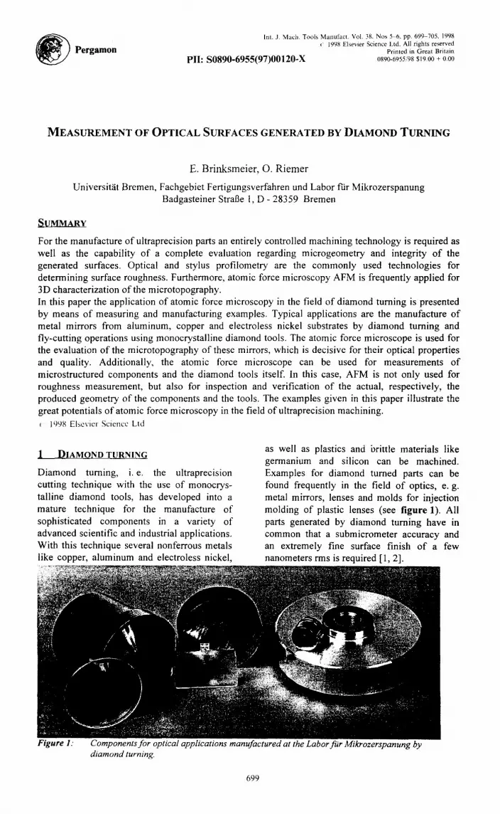
as well as plastics and brittle materials like germanium and silicon can be machined. Examples for diamond turned parts can be found frequently in the field of optics, e.g. metal mirrors, lenses and molds for injection molding of plastic lenses (see figure 1). All parts generated by diamond turning have in common that a submicrometer accuracy and an extremely fine surface finish of a few nanometers rms is required [1, 2].
Figure 1: Components for optical applications manufactured at the Labor fiir Mikrozerspanung by diamond turning.
699
700 E. Brinksmeier and O. Riemer
For cutting processes the achievable form accuracy of the workpiece is mainly restricted by the machine tool error motions. The surface roughness is limited by the tool profile which is transfered into the workpiece as well as by process vibrations and microstructural material effects. As optical applications require both form accuracies being better than k/10 and surface roughness of less than ~,/100, ultraprecise machine tools and diamond tools, are essential prerequisites for diamond turning [1, 2]. In diamond turning ultraprecision machine tools with refined mechanical elements, dedicated designs and special metrology and control features are operated in controlled environments. Besides, high quality tools made from monocrystal diamonds showing nanometric edge sharpness, reproducible shapes and high wear resistance are applied. There are two principle kinds of machining operations, the turning and the fly-cutting process, in which, respectively the workpiece or the diamond tool is rotated on the main spindle. Additionally to ultraprecision machine tools, high quality diamond tools, dedicated control systems and environmental controlled housings a refined metrology is indispensable for examination and quality control of the diamond tools and the machined parts. Commonly the inspection of the achieved
surface texture is carried out using light microscopy, profilometry or SEM. Form accuracy can be checked out with interferometers or coordinate measuring machines [2, 3]. Furthermore, in recent years atomic force microscopy (AFM) has turned into an approved measuring technique for determining surface topographies of smooth surfaces [4]. In this paper the application of AFM for measuring the surface roughness of diamond turned parts as well as examining diamond turned microstructures is presented.
2 ATOMIC FORCE MICROSCOPY
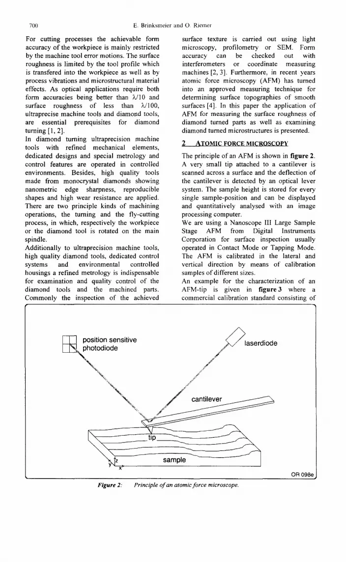
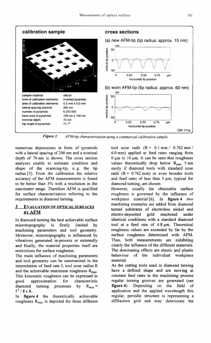
The principle of an AFM is shown in figure 2. A very small tip attached to a cantilever is scanned across a surface and the deflection of the cantilever is detected by an optical lever system. The sample height is stored for every single sample-position and can be displayed and quantitatively analysed with an image processing computer. We are using a Nanoscope III Large Sample Stage AFM from Digital Instruments Corporation for surface inspection usually operated in Contact Mode or Tapping Mode. The AFM is calibrated in the lateral and vertical direction by means of calibration samples of different sizes. An example for the characterization of an AFM-tip is given in figure3 where a commercial calibration standard consisting of
~ . ph.position sensitive todiode
-%. "~%%,
.,~laserdiode /
/
\ , . 1 I/ c a n t i l e v e ~ "~~- \ ~
Figure 2: Principle of an atomic force microscope.
OR 098~
Measurement of optical surfaces 701
calibration sample
sample material: term of calibration elements: area of calibration elements: lateral spacing (period): number of pyramids:
base area of pyramids: nominal depth: top angle of pyramids:
silicon inverted pyramids
0.5 mm x 0.5 mm 200 nm 6 250 000
100 nm x 100 nm 70 nm 71.1 °
cross sec t ions
(a) new AFM-tip (tip radius: approx. 15 nm) n m
g 5 ~
i
= 0
'E -5o- "
0 0.25 0.50 0.75 pm horizontal tip position
(b) worn AFM-tip (tip radius: approx. 60 nm) nm
.5 501
0 0.25 0.50 0.75 pm horizontal tip position
O R 111e
Figure 3. AFM-tip characterization using a commercial calibration sample.
numerous depressions in form of pyramids with a lateral spacing of 200 nm and a nominal depth of 70 nm is shown. The cross section analyses enable to estimate condition and shape of the scanning-tip, e.g. the tip radius [5]. From the calibration the relative accuracy of the AFM measurements is found to be better than 3% with a resolution in the nanometer range. Therefore AFM is qualified for surface characterization referring to the requirements in diamond turning.
3 EVALUATION OF OPTICAL SURFACES BY A F M
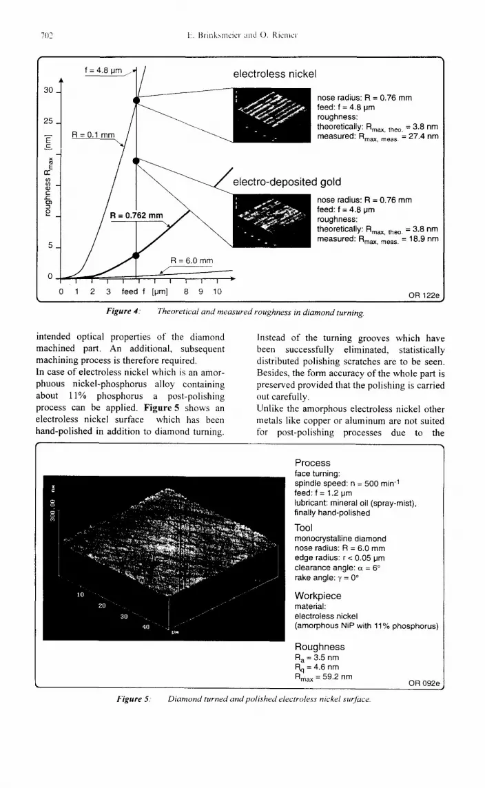
In diamond turning the best achievable surface microtopography is firstly limited by machining parameters and tool geometry. Moreover, microtopography is influenced by vibrations generated in-process or externally and finally, the material properties itself are restrictions for surface roughness. The main influence of machining parameters and tool geometry can be summarized in the interrelation of feed rate f, tool nose radius R and the achievable maximum roughness Rmax. This kinematic roughness can be expressed in good approximation for characteristic diamond turning processes by Rma x = f 2 / 8 o R . In figure 4 the theoretically achievable roughness Rma x is depicted for three different
tool nose radii (R = 0.1 m m / 0 .762mm/ 6.0 mm) applied at feed rates ranging from 0 p.m to 10 ~tm. It can be seen that roughness values theoretically drop below Rmax 5 nm easily if diamond tools with standard nose radii (R= 0.762 mm) or even broader tools and feed rates of less than 5 pm, typical for diamond turning, are chosen. However, usually the obtainable surface roughness is governed by the influence of workpiece material [6]. In f igure4 two machining examples are added from diamond turned substrates of electroless nickel and electro-deposited gold machined under identical conditions with a standard diamond tool at a feed rate of 4.8 lam. Theoretical roughness values are exceeded by far by the surface roughness determined with AFM. Thus, both measurements are exhibiting clearly the influence of the different materials. The dominating effects are elastic and plastic behaviour of the individual workpiece material. As the cutting tools used in diamond turning have a defined shape and are moving at constant feed rates in the machining process regular turning grooves are generated (see figure 4). Depending on the field of application and the applied wavelength this regular, periodic structure is representing a diffraction grid and may deteriorate the
702 E. Brinksmeier zlnd O. Ricmcr
nose radius: R = 0.76 mm feed: f = 4.8 pm roughness: theoretically: Rmax, theo. = 3.8 nm measured: Rmax , meas. = 27.4 nm
d gold
nose radius: R = 0.76 mm feed: f = 4.8 pm roughness: theoretically: Rmax, theo. -- 3.8 nm measured: Rmax, meas. = 18.9 nm
0 1 2 3 feed f [um] 8 9 10
Figure 4. Theoretical and measured roughness in diamond turning.
OR 122e
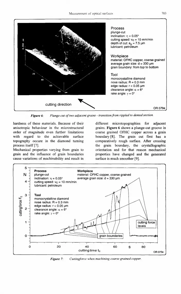
intended optical properties of the diamond machined part. An additional, subsequent machining process is therefore required. In case of electroless nickel which is an amor- phuous nickel-phosphorus alloy containing about 11% phosphorus a post-polishing process can be applied. Figure 5 shows an electroless nickel surface which has been hand-polished in addition to diamond turning.
Instead of the turning grooves which have been successfully eliminated, statistically distributed polishing scratches are to be seen. Besides, the form accuracy of the whole part is preserved provided that the polishing is carried out carefully. Unlike the amorphous electroless nickel other metals like copper or aluminum are not suited for post-polishing processes due to the
P r o c e s s face turning: spindle speed: n = 500 min q feed: f = 1.2 um lubricant: mineral oil (spray-mist), finally hand-pol ished
Tool monocrystal l ine diamond nose radius: R = 6.0 mm edge radius: r < 0.05 pm clearance angle: cc = 6 ° rake angle: y = 0 °
Workpiece material: electroless nickel (amorphous NiP with 11% phosphorus)
Roughness R a = 3.5 nm Rq= 4.6 nm
max = 59.2 nm OR 092e
Figure 5. Diamond turned and polished electroless nickel surlace.
Measurement of optical surfaces 703
cut t ing d i rec t ion
P rocess plunge-cut inclination: 11 = 0.05 ° cutting speed: vc = 10 mm/min depth of cut: ap = 7.5 um lubricant: petroleum
W o r k p i e c e material: OFHC copper, coarse grained average grain size: d = 330 um grain boundary: from top to bottom
Tool monocrystalline diamond nose radius: R = 0.3 mm edge radius: r < 0.05 um clearance angle: c~ = 6 ° rake angle: ), = 0 °
OR 079e
Figure 6:
hardness of these materials. Because of their anisotropic behaviour in the microstructural order of magnitude even further limitations with regard to the achievable surface topography occure in the diamond turning process itself [7]. Mechanical properties varying from grain to grain and the influence of grain boundaries cause variations of machinability and result in r
Plunge-cut o f two adjacent grains - transition from rippled to dented section.
different microtopographies for adjacent grains. Figure 6 shows a plunge-cut groove in coarse grained OFHC copper across a grain boundary[8]. The grain cut first has a comparatively rough surface. After crossing the grain boundary, the crystallographic orientation and for that reason mechanical properties have changed and the generated surface is much smoother [9].
5
N
4 -
3 u~ o } .o .£o ~ 2
o =
Process plunge-cut inclination: ~1 = 0.05 ° average grain size: d = 330 um cutting speed: vc = 10 mm/min lubricant: petroleum
Tool ~ / I ~ f I monocrystalline diamond / I/1,/ I nose radius: R = 0.3 mm / II ~ J edge radius:r< 0.05 pore I /I clearance angle: c~ = 6 ,4 rake ang ~
,, .: .... ~-,-r"'*"""- ~ grain boundaries]
Workpiece material: OFHC copper, coarse grained
cutting force levels
20 40 60 S 80 cut t ing t ime tc OR 073e
Figure 7: Cuttingforce when machining coarse grained copper.
704 E. Brinksmeier and O. Riemer
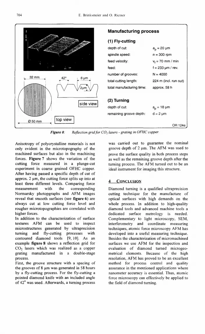
:i' 32 mm___~: ~' 42°- *" t* 8 pm ,i
Is'de viewl
,, E~ 50 mm ' t o p v i e w
M a n u f a c t u r i n g p r o c e s s
(1) Fly-cutting
depth of cut:
spindle speed:
feed velocity:
feed:
number of grooves:
total cutting length:
total manufacturing time:
ap = 20 IJm
n = 300 rpm
vf = 70 mrn / min
f = 233 IJm / rev.
N = 4000
224 m (incl. run out)
approx. 58 h
(2) Turning
depth of cut:
remaining groove depth:
ap = 18 IJm
d=21Jm
OR 124e
Figure 8: Reflection grid for C02
Anisotropy of polycrystailine materials is not only evident in the microtopography of the machined surfaces but also in the machining forces. Figure 7 shows the variation of the cutting force measured in a plunge-cut experiment in coarse grained OFHC copper. After having passed a specific depth of cut of approx. 2 gm, the cutting force splits up into at least three different levels. Comparing force measurement with the corresponding Normarsky photopgraphs and AFM images reveal that smooth surfaces (see figure 6) are always cut at low cutting force level and rougher microtopographies are correlated with higher forces, In addition to the characterization of surface textures AFM can be used to inspect microstructures generated by ultraprecision turning and fly-cutting processes with contoured diamond tools [9, 10]. As an example figure 8 shows a reflection grid for CO2 lasers which was realized as a copper grating manufactured in a double-stage process. First, the groove structure with a spacing of the grooves of 8 p.m was generated in 58 hours by a fly-cutting process. For the fly-cutting a pointed diamond knife with an included angle of 42 ° was used. Afterwards, a turning process
lasers - grating in OFHC copper.
was carried out to guarantee the nominal groove depth of 2 gm. The AFM was used to
prove the surface quality in both process steps as well as the remaining groove depth after the turning process. The AFM turned out to be an ideal instrument for imaging this structure.
4 CONCLUSION
Diamond turning is a qualified ultraprecision cutting technique for the manufacture of optical surfaces with high demands on the whole process. In addition to high-quality diamond tools and advanced machine tools a dedicated surface metrology is needed. Complementary to light microscopy, SEM, interferometry and coordinate measuring techniques, atomic force microscopy AFM has developed into a useful measuring technique. Besides the characterization of micromachined surfaces we use AFM for the inspection and evaluation of diamond turned microgeo- metrical elements. Because of the high resolution, AFM has proved to be an excellent method for process control and quality assurance in the mentioned applications where nanometer accuracy is essential. Thus, atomic force microscopy can effectively be applied to the field of diamond turning.
Measurement of optical surfaces 705
[1] N. Ikawa; R. R. Donaldson; R. Komanduri; W. K6nig; P. A. McKeown; T. Moriwaki; I. F. Stowers. "Ultraprecision Metal Cutting - The Past, the Present and the Future". Annals of the CIRP Vol. 40, 2/1991: p. 587-594.
[2] E. Brinksmeier. "Hersteilung yon Pr'~izisionsbauteilen durch Mikrozer- spanung". IDR 4/1994: p. 210-217.
[3] E. Brinksmeier; W. Preul3; O. Riemer; M. Schroeder. "Manufacturing and Measurement of Elliptical Mirrors for Focussing Synchrotron Radiation". Proc. 8th IPES, Compiegne, France, May 1995, Elsevier, 1995: p. 459-462.
[4] G. Binnig: "Force Microscopy". Ultramicroscopy 42-44, 1992: p 7.
[5] S.S. Sheiko, M. M611er, E. M. C. M. Reuvekamp, H. W. Zandbergen. "Evaluation of the Probing Profile of Scanning Force Microscopy Tips". Ultramicroscopy 53, 1993: p. 371-380.
[6] Rentsch, R; I. Inasaki; E. Brinksmeier; W. PreuB; O. Riemer. ,,Influence of Material Characteristics on the Micromachining Process". Materials Issues in Machining-III (ed. D. A.
Stephenson and R. Stenvenson), Fall Meeting of TMS, Cincinnati, Ohio, October 6-10, 1996: p. 65-86.
[7] Brinksmeier, E; W. PreuB; O. Riemer; J. Schmiitz. ,,Effect of Grain Orientation and Grain Boundaries on the Surface Topography of Diamond Turned OFHC Copper". Proc. 1 lth Annual Meeting ASPE, 9-14 Nov. 1996, Monterey, USA: p. 506-509.
[8] E. Brinksmeier; W. PreuB; O. Riemer. "From Friction to Chip Removal. An Experimental Investigation of the Microcutting Process. Part I ". Proc. 3rd Int. Conf. on Ultra Precision in Manufac- turing Engineering; Hrsg: M. Weck, H. Kunzmann, Verlag Franz Rhiem, Duisburg, 1994: p. 393-400.
[9] Weck, M.; J. Luderich; M. Vos; H. B. Schroeder. ,,Manufacturing of Micromechanical Components by Diamond Cutting - Limits and Chances". Proc. 8th IPES, Compiegne, France, May 1995, Elsevier, 1995: p. 431-434.
[10] Brinksmeier, E; R. Malz. ,,Manufacturing and Measurement of Microstructures using Ultraprecision Machining and Atomic Force Microscopy". ACTUATOR 96, 5th Int. Conf. on New Actuators, 26-28 June 1996, Bremen: p. 92-95.