Embed Size (px)
Citation preview

IEEE TRANSACTIONS ON ELECTRON DEVICES, VOL. 45, NO. 6, JUNE 1998 1369
Measurement of the Switching Speed of Single FET’sKeith A. Jenkins and Joachim N. Burghartz
Abstract—The measurement of the signal delay through asingle FET as an estimate of its performance is discussed. It isshown that instead of relying on small ac signals for performancecharacterization, delays of full logic swings can be accuratelymeasured with conventional electronic equipment. The measure-ment apparatus is described, and data obtained with advancedsubmicron FET’s is presented, showing that device switchingdelays can be measured with resolution on the order of 10 ps.Such device delay measurements can be of use in evaluatingtechnologies, and diagnosing performance problems.
Index Terms—Device delay, large signal, measurement, propa-gation delay, signal delay, switching speed, time domain.
I. INTRODUCTION
TWO complementary measurement methods are com-monly used to evaluate the digital switching speed
of today’s transistors for the purpose of estimating theirperformance in circuits. One is the measurement of the smallsignal, high-frequency S-parameters, from which figures ofmerit, such as f and f are derived, and from which smallsignal equivalent-circuit models of the transistors can beconstructed. Combining these data with the dc characteristicsof the device, it is possible to predict, by numerical simulation,the time-domain response of the device to a large signal swing.The other method is to make a simple circuit of many identicaltransistors, for example, a chain, or a ring of logic gates. Thepropagation delay through this large number of devices iseasily measured, and from this experimental measure of theaverage delay, the individual gate delay can be deduced.
Both methods have advantages and disadvantages. TheS-parameter method is very useful for detailed device model-ing. Its chief disadvantage is that it only provides small signalinformation. The response of the device to the full voltageswing of digital circuits can not be directly obtained. Mostdigital circuit simulators, in fact, are based on dc data. Whilethe measurement of a chain of devices overcomes the smallsignal limitation, it has the drawback that it yields essentiallyno diagnostic information. It requires a predetermined choiceof logic gates, and demonstrates only the average deviceperformance in a large set. In addition, such test sites canconsume large wafer areas.
Measurement of large signal propagation through singletransistors is an alternative approach which combines some ofthe advantages of both methods described above. Such mea-surements can be used to compare device speed, and to provideinformation for diagnosing problems, even without resortingto device models. In addition, large signal measurements may
Manuscript received June 13, 1997; revised October 22, 1997. The reviewof this paper was arranged by Editor D. P. Verret.
The authors are with the IBM T. J. Watson Research Center, YorktownHeights, NY 10598 USA.
Publisher Item Identifier S 0018-9383(98)03678-8.
be more suitable for comparison with device simulations. It isshown below that these measurements can be useful for char-acterizing advanced submicron devices which switch in lessthan 50 ps. The paper describes the measurement strategy, andthe apparatus required to make such measurements. The pulsedelay technique has been applied to silicon MOSFET’s, andthe discussion below is focused on these types of transistors.
II. I NSTRUMENTATION
The goal of the measurement is to apply a pulse with a shortrisetime to the gate of the FET and to measure the responseof the transistor with a time resolution sufficient to see thesignal delay through the transistor. The applied pulse has anamplitude equal to the logical “1” level. For today’s advancedMOSFET technologies, as will be seen below, the time scalerequired of such measurements is on the order of tens of ps.Several techniques have been reported which use short opticalpulses from lasers, combined with photoconductive switchesand electro-optic crystals, to acquire voltages with superbtime resolution [1]–[5]. However, these techniques have notgained wide acceptance, for a variety of reasons, includingpoor control of the applied signal amplitude, uncertainty ofthe output voltage, the need for specialized layout or fixtur-ing, inconvenient apparatus, and device loading. High timeresolution electron-beam probing is another possible technique[6], [7], but also suffers from lack of convenience, and hasapparently not been used for transistor characterization. Whilethe time resolution of electrical measurements is not as fineas that of optical techniques, it is adequate for pulse delaymeasurements.
The instrumentation required for short time domain mea-surements is illustrated in the diagram of Fig. 1. Conven-tional high bandwidth equipment can be used to generate andmeasure the pulses, but to measure delays of contemporarysubmicron FET’s, care must be taken to preserve and measurethe pulses with high fidelity. The time resolution requirednecessitates the use of high bandwidth transmission lines andcomponents for the propagation of stimulus and responsesignals. All the signal connections in this figure are made with50 coaxial cable. In principle, any length of cable can beused, but degradation of signal transition time increases asthe cables get longer. In this work, all cables were 1 m orless. The gate of the FET is driven by a pulse from a pulsegenerator which has a risetime of less than 50 ps, and anamplitude of several volts. Changes in the voltage level ofthis signal can be either set on the pulse generator, or setwith coaxial attenuators. Components and connectors must allhave a bandwidth of 18 GHz or higher (transition times ofless than 20 ps). SMA connectors on high-quality cables aresufficient for interconnections. A 10 in-line probe, which is
0018–9383/98$10.00 1998 IEEE

1370 IEEE TRANSACTIONS ON ELECTRON DEVICES, VOL. 45, NO. 6, JUNE 1998
(a) (b)
Fig. 1. (a) Diagram of the measurement apparatus for high bandwidth pulse measurements. All connections between components, e.g., the signal from thepulse generator to the oscilloscope trigger, are made with 50 coaxial cables. (b) Equivalent circuit for high-frequency ac signals and rapid transients.
similar to a power divider, is connected for monitoring theinput signal, and its reflection. (This is the only componentwhich is not 50 . It has an impedance of about 45,and therefore causes slight reflections.) All other equipmentis matched to 50 , so reflections are absorbed. The pulseis delivered to the transistor through microwave probes. Abias “tee” is used to hold the drain terminal of the transistorto the desired value. A pulse on the gate causes a transientoutput signal on the drain terminal. The transient signal passesthrough the capacitor of the tee, while the inductor blocks it,so the tee looks like a transparent 50transmission line forhigh-frequency transients. The output and monitor signals aremeasured on a high bandwidth sampling oscilloscope.
A simplified equivalent ac or transient circuit is shownin Fig. 1(b). The inductor of the bias tee has a very highimpedance for high frequencies, or short transients, while thecapacitor has a very low impedance. Thus the tee applies adc voltage but is transparent to the transient signals. Hence,when the device switches from “off” to “on,” the characteristicimpedance, , of the transmission line (equal to 50)appears as a load from the terminal to the power supply,
. The 50 load is an unavoidable consequence of usingtransmission lines to propagate the signals. Although a 50load may be significantly different from the situation in a logiccircuit, this is of little consequence for evaluating the intrinsicspeed of devices. Only the “off” to “on” transition can beused to evaluate normal transistor performance. In an “on”to “off” transition, the voltage at the device terminal actuallyincreases, by , which may put the device voltage outsideits normal operating region. The distinction between thesecases is illustrated in Fig. 2. Because of the capacitor in thebias “tee,” the duty cycle (on time/off time) must be fairlylow to avoid a dc shift of the drain voltage. [If pulses areapplied repetitively, the voltage is changed by the amount
, where is the amplitude of the drain
Fig. 2. Demonstration of loadline under large signal pulse conditions, show-ing that the “on” to “off” transition (dashed line) puts the device outside thenormal operating region.
voltage pulse, is the pulse width, and is the pulse period.]The transistor itself must be specially designed for probing
in order to make these measurements. The same considerationsused in designing for high-frequency-parameter measure-ments apply here. In particular, the pads must be designedfor microwave probes with a common ground, while the gateand drain probe pads must be isolated from any other devices.Open and short calibration sites should be fabricated for timemarking the device pulses. In addition, the device itself shouldsatisfy two size limits.
1) It must be large enough so that its output currentproduces a sizable voltage across the 50load thatit drives
2) It must be small enough so that it switches into or nearthe saturation region (in order to mimic the situation ina digital circuit).

JENKINS AND BURGHARTZ: MEASUREMENT OF THE SWITCHING SPEED OF SINGLE FET’S 1371
Fig. 3. Measurement of response of nFET’s to a fast gate pulse, shown forthree different channel lengths. The arrow indicates the delay measured athalf the voltage swing.
The device width can be determined if the maximum draincurrent per device width can be estimated, and then convertingcurrent to voltage on the 50 load. A minimum of about100 mV, or 2 mA, is needed for a good signal. The maximumdevice size can be specified by defining a maximum acceptablevoltage drop below , which is probably on the order of1.0 V, or 20 mA, or less.
III. A PPLICATIONS
An example of measurements taken with this method isgiven in Fig. 3. These data are taken with devices from anadvanced technology having a supply voltage level of 1.8 V[8], [9]. The data were obtained with a sampling oscilloscopewith 20 GHz (18 ps) bandwidth, and a pulse generator with arise time of 15 ps. In this figure, the “input” signal is the pulseapplied to the gate. For a timing reference, the input signal isactually applied to a “through” structure on the wafer, andstored in the oscilloscope memory. The pulse is then appliedto the transistor of interest, where it doubles in amplitudesince the device gate is an open termination of the 50transmission line. This doubling can be observed with the10 monitor probe, which may also reveal problems withthe device, such as a shorted or resistive gate. The voltageon the drain constitutes the output signal, which appearson the oscilloscope and can be stored. The risetime of theinput signal is about 50 ps, compared to 15 ps coming fromthe pulse generator. About 20 ps of this degradation is dueto the probe pads and the silicon substrate losses, and theremainder is due to the components and connectors. The padshave a capacitance of about 350 fF, which is of the sameorder of magnitude as the device capacitance. In contrast toS-parameter measurements, there is no well-accepted way tode-embed the device response from these parasitic effects [10].This is presumably because the phase information is containedin the signal transition times, which are much less readilycharacterized than the phase of a sinusoidal waveform.
In Fig. 3, devices with three different channel lengths aredisplayed. Differences in switching speed due to the different
channel lengths are easily seen with resolution significantlybetter than 50 ps. With the parasitic effect of the probe padsremoved by calibration, the cutoff frequency of the shortestchannel devices in this technology is greater than 50 GHz,corresponding to a transit time of 3 ps. Clearly, the approx-imately 30 ps delay through the device produced by a fulllogic swing on the gate is far greater than this. This differencedemonstrates the well-known fact that although the small sig-nal response (cutoff frequency) is a valuable device parameterfor characterizing channel length, its numerical value cannotbe simply converted to a device time delay figure of merit.
In this example, all the devices have the same width (40m), and source/drain contact configuration, and differ only
in channel length. Thus, the differences in the output voltageamplitude are due to the difference in the transient draincurrent driving the 50 load. It can also be seen that theoutput fall time increases with channel length, which is anotherconsequence of the lesser drive current available from thetransistors with longer channel lengths. A digital delay figure-of-merit can be determined from these measurements by takingthe time difference between the midpoint voltage of the inputand output signals (the arrow in Fig. 3). Although such afigure-of-merit cannot be directly interpreted as the expecteddelay in a circuit, it is very useful for comparisons.
Such comparative information can be useful for studying avariety of device and process issues. Some examples are:
1) comparison of lithography methods,2) comparison of processing technologies,3) observation of the effect of temperature,4) determining the effect of threshold voltage on delay,5) measuring the delay caused by high drain resistance, and6) diagnosing poor transistor performance.
While some of these effects may be very effectively studiedwith S-parameter measurements, the small signal nature of S-parameters reveals only the properties of the device at somefixed bias. In contrast, a full-swing time-domain measurementincorporates all of the dynamic device properties in onewaveform. In some cases, time-domain measurements mayalso be easier to interpret. For example, the use of pulse delaymeasurements for diagnostics was given in [9], in which itwas shown that a discontinuity in a composite gate electrodecould severely degrade the speed of FET’s, even though therewas no measured reduction of the cutoff frequency, f.
Another example related to the gate technology shows theimportance of device geometry when a gate electrode withhigh resistance is used [11]. In this example, FET’s composedof ten parallel fingers of 10 m each were compared tothose composed of two parallel 20-m fingers. Devices madewith polysilicon gates and silicided gates were measured. Themeasurements of the pulse delays of these devices is shownin Fig. 4. Of the four device delays plotted, the - mpolysilicon-gate turn-on time is dramatically greater. Thisdifference is because the layout results in a factor of tendifference in the total gate resistance, which is significantfor resistive polysilicon gates. In contrast, with gates formedwith silicide, which is much less resistive than polysilicon, thedifferences in pulse delay due to layout were minor.
1372 IEEE TRANSACTIONS ON ELECTRON DEVICES, VOL. 45, NO. 6, JUNE 1998
Fig. 4. Response of nFET’s with polysilicon and silicide gates, using twodifferent layouts. Solid lines are the polysilicon gate devices, and dashedlines are the silicide gate devices.
Fig. 5. Measurement of the pulse response of nFET’s. The dashed lines arethe signal feeding through the “off” device (no drain voltage applied). The0.15-�m feedthrough signal is multiplied by 20; the 0.60�m by 10.
While the propagation delay through devices in this mannercan be very useful for comparisons and problem determination,it does not accurately measure the input to output devicedelay. This is because the signal to the device gate is delayedsomewhat by the device capacitance and that of the probepads. For accurate measurements of device delay, this delaymust be taken into account. This delay can be seen by lookingat the reflected signal measured with the 10monitor probe.Reflection from open pads (probe pads without transistors)establishes a reference time. The reflected signals of largedevices arrive at the oscilloscope later than that of smallerdevices, due to the slowing effect of the capacitance. Thesereflections can be used to construct corrections to bring theoutput signals to a common starting time. The use of smallerdevices and smaller probe pads can reduce the magnitude ofthis adjustment. Devices built on insulating substrates, such asSOI (silicon-on-insulator) may not need any correction, sincethe devices themselves have smaller capacitance.
However it is simpler to measure this delay using a signalpassing through the “off” device, that is when its drainvoltage is zero. In this case, the device capacitance provides
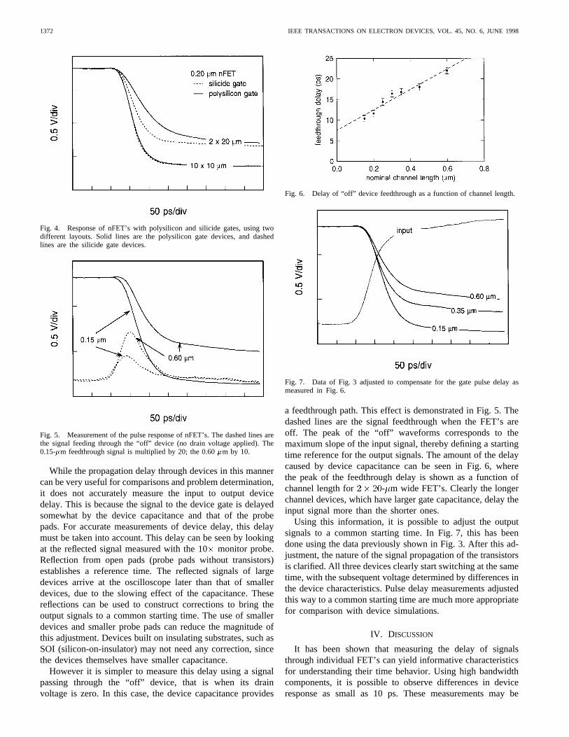
Fig. 6. Delay of “off” device feedthrough as a function of channel length.
Fig. 7. Data of Fig. 3 adjusted to compensate for the gate pulse delay asmeasured in Fig. 6.
a feedthrough path. This effect is demonstrated in Fig. 5. Thedashed lines are the signal feedthrough when the FET’s areoff. The peak of the “off” waveforms corresponds to themaximum slope of the input signal, thereby defining a startingtime reference for the output signals. The amount of the delaycaused by device capacitance can be seen in Fig. 6, wherethe peak of the feedthrough delay is shown as a function ofchannel length for - m wide FET’s. Clearly the longerchannel devices, which have larger gate capacitance, delay theinput signal more than the shorter ones.
Using this information, it is possible to adjust the outputsignals to a common starting time. In Fig. 7, this has beendone using the data previously shown in Fig. 3. After this ad-justment, the nature of the signal propagation of the transistorsis clarified. All three devices clearly start switching at the sametime, with the subsequent voltage determined by differences inthe device characteristics. Pulse delay measurements adjustedthis way to a common starting time are much more appropriatefor comparison with device simulations.
IV. DISCUSSION
It has been shown that measuring the delay of signalsthrough individual FET’s can yield informative characteristicsfor understanding their time behavior. Using high bandwidthcomponents, it is possible to observe differences in deviceresponse as small as 10 ps. These measurements may be

JENKINS AND BURGHARTZ: MEASUREMENT OF THE SWITCHING SPEED OF SINGLE FET’S 1373
useful for comparison with device simulations. However, asshown above, even without simulations, the measurements arequite useful for comparing the switching speed of transistorsas a function of various factors. As such, the measurementtechnique can be useful for routine measurements of deviceperformance, and is suitable for automation. Typically, wafersin the development process include S-parameter measurementsites, which can be adapted for these time domain measure-ments, thus requiring no additional area.
It is interesting to ask if this pulse delay technique willcontinue to be useful as faster and faster devices are fabricated.The time resolution is limited by the rise and fall times of thesignals, which may be limited by the bandwidth of the coaxialcomponents and of the oscilloscope. The input pulse is limitedby the pulse generator, the bandwidth of the components, andby the device pad capacitance. In the data shown here, theresolution and pulse limitation are shown by the degradation ofthe 15 ps pulse of the pulse generator to the 50 ps pulse whichis observed. Higher bandwidth components and oscilloscopesare presently available, and their net contribution to resolutioncould probably be reduced to 20 ps. The pad capacitance ofthe device is affected by the substrate and the pad size. Areduction in input pad size translates directly into a reductionin capacitance. In this work, the - m pads, overan oxide of 700 nm, have a capacitance of about 350 fF.Smaller pads could limit this contribution to about 15 ps,so the net degradation could be reduced to about 30 ps.The use of an insulating substrate, which is seen by someworkers as an additional way of improving MOS device speed,makes further improvements in the pulse edge possible. Theapparatus described here has been used to produce inputpulses of 30 ps on SOI devices. Microstrip probing padsmay reduce transition times even more. Further improvementsmight require development of faster pulse generators andhigher bandwidth components.
However, it is noted that with the approximately 50 ps inputpulse which is obtained with the system described here, themeasured response of the devices is not limited by instrumentresolution. It is possible to measure useful differences in deviceresponse with an apparent resolution of 10 ps. Hence, theprincipal result of an improvement in the system bandwidthwould be a sharper input pulse, thereby improving absolutedelay measurement. Greater bandwidth would also make thetask of numerical modeling simpler. Reduction of output padcapacitance would also lead to a sharper output pulse, alsoimproving the overall measurement precision.
ACKNOWLEDGMENT
The authors would like to thank E. F. Crabbe, D. F. Heidel,and G. G. Shahidi for useful discussions of the topics discussedin this paper.
REFERENCES
[1] D. H. Auston, “Picosecond optoelectronic switching and gating insilicon,” Appl. Phys. Lett.,vol. 26, pp. 101–103, 1975.
[2] G. D. Anderson, R. W. Dutton, J. D. Morse, and R. P. Mariella, “On-chip picosecond time-domain measurement of silicon bipolar transistor
characteristics using integrated GaAS photoconductive devices,” inIEDM Tech. Dig.,1991, pp. 37–40.
[3] J. A. Valdmanis, G. A. Mourou, and C. W. Gabel, “Picosecond electro-optic sampling system,”Appl. Phys. Lett.,vol. 41, pp. 211–212, 1982.
[4] M. Matloubian, H. Fetterman, M. Kim, A. Oki, J. Camou, S. Moss, andD. Smith, “Picosecond optoelectronic measurement of S parameters andoptical response of an AlGaAs/GaAs HBT,”IEEE Trans. MicrowaveTheory Tech., vol. 38, pp. 683–686, May 1990.
[5] R. B. Marcus, Ed.,Measurement of High-Speed Signals in Solid StateDevices. San Diego, CA: Academic, 1990, chs. 3–5.
[6] M. Brunner, D. Winkler, R. Schmitt, and B. Lischke, “Electron-beam testsystem for high-speed devices,”Scanning,vol. 9, pp. 201–204, 1987.
[7] A. J. Fixl and K. A. Jenkins, “Laser stimulated photocathode electronbeamprober for 15 ps resolution waveform measurements,” inProc. 4thEurop. Conf. Electron and Optical Beam Testing of Electronic Devices,Sept. 1993, pp. 81–88.
[8] G. G. Shahidi, J. Warnock, A. Acovic, P. Agnello, C. Blair, T. Bucelot,J. Burghartz, E. Crabb´e, J. Cressler, P. Coane, J. Comfort, B. Davari,S. Fischer, E. Ganin, S. Gittleman, J. Keller, K. Jenkins, D. Klaus, K.Kwietniak, T. Lii, P. A. McFarland, T. Ning, M. Polcari, S. Subbanna,J. Y. Sun, D. Sunderland, A. C. Warren, and C. Wong, inDig. Tech.Papers 1993 Symp. VLSI Technol., 1993, pp. 93–94.
[9] K. A. Jenkins, J. N. Burghartz, and P. D. Agnello, “Identification of gateelectron discontinuities in submicron CMOS technologies, and effecton circuit performance,”IEEE Trans. Electron Devices,vol. 43, pp.759–765, May 1996.
[10] L. A. Hayden and V. K. Tripathi, “Calibration methods for time domainnetwork analysis,”IEEE Trans. Microwave Theory Tech., vol. 41, pp.415–420, Mar. 1993.
[11] B. Razavi, R.-H. Yan, and K. F. Lee,IEEE Trans. Circuits Syst. I, vol.41, pp. 750–754, Nov. 1994.
Keith A. Jenkins received the Ph.D. degree in physics from ColumbiaUniversity, New York, NY, for work done in experimental high-energyphysics.
He continued his work in the field of experimental high-energy physicsat Rockefeller University, New York, until 1983, when he joined the IBMResearch Division at the T. J. Watson Research Center, Yorktown Heights,NY, where he first worked in Josephson technology. He later joined the SiliconTechnology Department, where he worked in a variety of device and circuitsubjects, including high-frequency measurement techniques, electron beamcircuit testing, radiation-device interactions, and low-temperature electronics.Currently, he is a Senior Engineer at the IBM T. J. Watson Research Center,and a member of the VLSI Systems Department. His current activities includeevaluation of the performance of VLSI circuits, phase-locked loops, andintegrated silicon RF circuits, and research into the transient behavior ofsilicon-on-insulator (SOI) FET’s.
Joachim N. Burghartz received the Dipl.Ing. de-gree from the Technische Hochschule Aachen, Ger-many, in 1982, and the Ph.D. degree from theUniversity of Stuttgart, Germany, in 1987, both inelectrical engineering.
From 1982 to 1987, he was with the Universityof Stuttgart, where he developed sensors with in-tegrated signal conversion with a special focus onmagnetic-field sensors. Since 1987, he has been withthe IBM T. J. Watson Research Center, YorktownHeights, NY. His earlier research work at IBM
included device applications of selective epitaxial growth of silicon, Si andSiGe high-speed transistor design and integration processes, and 0.15-�mCMOS technology. For the past few years, he has been engaged in thedevelopment of circuit building blocks for SiGe rf front-ends, with a specialinterest in the integration of high-quality passive components on silicon. Hehas authored or coauthored more than 70 technical publications and holdsfive U.S. patents.
Dr. Burghartz has served at technical conferences such as IEDM, ESS-DERC, and BCTM.