Embed Size (px)
Citation preview

Portland State University Portland State University
PDXScholar PDXScholar
Dissertations and Theses Dissertations and Theses
6-2-1993
Measurement Techniques for Noise Figure and Gain Measurement Techniques for Noise Figure and Gain
of Bipolar Transistors of Bipolar Transistors
Wayne Kan Jung Portland State University
Follow this and additional works at: https://pdxscholar.library.pdx.edu/open_access_etds
Part of the Electrical and Computer Engineering Commons
Let us know how access to this document benefits you.
Recommended Citation Recommended Citation Jung, Wayne Kan, "Measurement Techniques for Noise Figure and Gain of Bipolar Transistors" (1993). Dissertations and Theses. Paper 4592. https://doi.org/10.15760/etd.6476
This Thesis is brought to you for free and open access. It has been accepted for inclusion in Dissertations and Theses by an authorized administrator of PDXScholar. Please contact us if we can make this document more accessible: [email protected].

AN ABSTRACT OF THE THESIS OF Wayne Kan Jung for the Master of Science in
Electrical and Computer Engineering presented June 2, 1993.
Title: Measurement Techniques for Noise Figure and Gain of Bipolar Transistors.
APPROVED BY THE MEMBERS OF THE THESIS COMMITTEE:
Paul vail Hal en, Chair
i
Branimir Pejcinovic
Pavel Smejtek
First, the concepts of reflection coefficients, s-parameters, Smith chart, noise
figure, and available power gain will be introduced. This lays out the foundation for the
presentation of techniques on measuring noise figure and gain of high speed bipolar
junction transistors. Noise sources in a bipolar junction transistor and an equivalent
circuit including these noise sources will be presented. The process of determining the
noise parameters of a transistor will also be discussed. A Pascal program and several
TEKSPICE scripts are developed to calculate the stability, available power gain, and
noise figure circles. Finally, these circles are plotted on a Smith chart to give a clear
view of how a transistor will perform due to a change in source impedances.
MEASUREMENT TECHNIQUES FOR NOISE FIGURE AND GAIN OF
BIPOLAR TRANSISTORS
by
WAYNE KAN JUNG
A thesis submitted in partial fulfillment of the requirements for the degree of
MASTER OF SCIENCE in
ELECTRICAL AND COMPUTER ENGINEERING
Portland State University 1993

TO THE OFFICE OF GRADUATE STUDIES:
The members of the Committee approve the thesis of Wayne Kan Jung
presented June 2, 1993.
APPROVED:
,<')
Paul ~n, Chair
Branimir Pejcmovic
Pavel Smejtek
Rolf Schaumann, Chair, Department of Electrical Engineering
Roy W. Kpch, Vice Provost for Graduate Studies and Research

ACKNOWLEDGEMENTS
I would like to take this opportunity to thank those who help make thesis
possible. First, I deeply appreciate my academic advisor Dr. Paul Van Halen for his
guidance and support throughout the completion of this thesis. Second, I thank my
mentor John Brewer, manager of Wireless Telecommunication Product Group of
Tektronix' Micro-Product Line, and other engineers from Tektronix: James M~sh, Ken
Weigel, Shaun Simpkins, and Tim Davis, for their guidance and support for completing
this work. Finally, special thanks are due to Dr. Branimir Pejcinovic and Dr. Pavel
Smejtek of Portland State University for their interest and support.

TABLE OF CONTENTS
PAGE
ACKNOWLEDGEMENTS ............................................. iii
LIST OF TABLES .................................................... vi
LIST OF FIGURES ................................................... vii
CHAPTER
I INTRODUCTION . . . . . . . . . . . . . . . . . . . . . . . . . . . . . . . . . . . . . . . . 1
Purpose of the Analysis . . . . . . . . . . . . . . . . . . . . . . . . . . . . . . 1
Outcome of the Analysis . . . . . . . . . . . . . . . . . . . . . . . . . . . . . 2
II EXPLANATION OF TERMS ............................... 4
S-parameters ...................................... 4
Introduction Reflection Coefficients S-parameters Smith Chart
Noise ............................................ 11
Common Types of Noise Noise Figure
Available Power Gain ............................... 14
III NOISE FIGURE MEASUREMENT .......................... 16
Noise in Bipolar Transistor ........................... 16
Flicker Noise Burst Noise Shot Noise Thermal Noise Equivalent Circuit

Determination of Noise Parameters . . . . . . . . . . . . . . . . . . . . . 20
Definition Source Impedance Selections Noise Figure Measurement from TEKSPICE Noise Parameters Computation
Noise Figure Circles . . . . . . . . . . . . . . . . . . . . . . . . . . . . . . . . 28
Comparison ....................................... 32
IV GAIN MEASUREMENT .................................. 37
Gain and Stability . . . . . . . . . . . . . . . . . . . . . . . . . . . . . . . . . . 37
Stability Criterion Stability Circles Gain Circles
S-parameters from TEKSPICE . . . . . . . . . . . . . . . . . . . . . . . . 42
Comparison . . . . . . . . . . . . . . . . . . . . . . . . . . . . . . . . . . . . . . . 44
V CONCLUSION .......................................... 54
REFERENCES ...................................................... 55
APPENDICES
A CONSTRUCTION AND APPLICATION OF
SMITH CHART .................................... 57
B NOISE FIGURE CALCULATIONS .......................... 62
C NOISE PARAMETERS AND NOISE FIGURE CIRCLES
CALCULATIONS .................................. 65
D STABILITY CIRCLES COMPUTATIONS .................... 75
E GAIN CIRCLES COMPUTATIONS ......................... 79
F S-PARAMETERS EXTRACTION ........................... 82
v

TABLE
I.
II.
LIST OF TABLES
PAGE
Noise Figure Measured at Various Source Impedances
with VBE=0.8V, V cE=4V at Frequency=lGHz . . . . . . . . . 24
Noise Parameters of N16 and G 14V102 Transistors . . . . . . . . . . . 28

FIGURE
1.
2.
3.
4.
5.
6.
7.
8.
9.
10.
11.
12.
13.
14.
15.
LIST OF FIGURES
PAGE
A General Two-port Network . . . . . . . . . . . . . . . . . . . . . . . . . . . . 5
Traveling Waves . . . . . . . . . . . . . . . . . . . . . . . . . . . . . . . . . . . . . . . 6
Incident and Reflected Waves in a Two-port Network . . . . . . . . . 8
The Smith Chart........................................ 10
Noise Figure of Network in Cascade . . . . . . . . . . . . . . . . . . . . . . . 13
Available Power Gain of a Two-port Network . . . . . . . . . . . . . . . 14
Bipolar Transistor Small-signal Equivalent Circuit
with Noise Sources . . . . . . . . . . . . . . . . . . . . . . . . . . . . . . 18
Noise Figure vs. Frequency for N16 . . . . . . . . . . . . . . . . . . . . . . . 19
Parabolic Noise Surface . . . . . . . . . . . . . . . . . . . . . . . . . . . . . . . . . 21
Test Circuit for Noise Figure . . . . . . . . . . . . . . . . . . . . . . . . . . . . . 23
Noiseless Resistor Model . . . . . . . . . . . . . . . . . . . . . . . . . . . . . . . . 24
Constant Noise Figure Circles for N16 with
VBE=0.8V, VcE=4V at Frequency=1GHz ............. 31
Constant Noise Figure Circles for Nl6 with
VBE=0.76V, V cE=4V at Frequency=900MHz . . . . . . . . . . 33
Constant Noise Figure Circles for G14V102 with
VBE=0.76V, V cE=4V at Frequency=900MHz . . . . . . . . . . 34
Constant Noise Figure Circles for N16 with
VBE=0.76V, V cE=4V at Frequency=1.6GHz . . . . . . . . . . 35

viii
FIGURE PAGE
16. Constant Noise Figure Circles for G14V102 with
VBE=0.76V, V cE=4V at Frequency=1.6GHz . . . . . . . . . . 36
17. Common Emitter Amplifier with Local Series Feedback . . . . . . . 37
18. Stability Circles Construction on Smith Chart ............... 40
19. Stability Region for r s • . • . . • . . . . . . • . . • . • . . . . . . . • • . . . . . • . 41
20. Test Circuit for Obtaining S 11 and S21 . . . . . . . . . . . . . . . . . . . . . . 43
21. Test Circuit for Obtaining S22 and S12 ...................... 44
22. Magnitude of Su for N16 ............................... 45
23. Phase of S11 for N16 ................................... 46
24. Magnitude of S12 for N16 . . . . . . . . . . . . . . . . . . . . . . . . . . . . . . . 46
25. Phase of S12 for N16 ................................... 47
26. Magnitude of S21 for N16 ............................... 47
27. Phase of S21 for N16 ................................... 48
28. Magnitude of S22 for N16 ............................... 48
29. Phase of S22 for N16 ................................... 49
30. Gain and Stability Circles for N 16 at
Frequency=900MHz ............................. 50
31. Gain and Stability Circles for G14V102 at
Frequency=900MHz . . . . . . . . . . . . . . . . . . . . . . . . . . . . . 51
32. Gain and Noise Figure Circles for N16 at
Frequency=900MHz ............................. 52
33. Gain and Noise Figure Circles for G 14V102 at
Frequency=900MHz . . . . . . . . . . . . . . . . . . . . . . . . . . . . . 53
34. Smith Chart Construction . . . . . . . . . . . . . . . . . . . . . . . . . . . . . . . 59

FIGURE
35.
36.
ix
PAGE
A Complete Smith Chart . . . . . . . . . . . . . . . . . . . . . . . . . . . . . . . . 60
Flow Chart for Noise Parameters Calculation . . . . . . . . . . . . . . . . 64

CHAPTER I
INTRODUCTION
In all things on earth there exists a degree of randomness. In the world of
electronics, the random nature of electric current has been known for over a hundred
years. It is a fact that no electronic system is completely free of random noise. Small
voltage fluctuations due to noise are always occurring in electronic circuits because
electrons are discrete and are constantly moving in time. The term "noise" originated
with the study of high-gain audio-frequency amplifiers. When a fluctuating voltage or
current generated in a device is amplified by an audio-frequency amplifier and the
amplified signal is fed into a loudspeaker, the loudspeaker produces a hissing sound,
hence the name noise. This descriptive term, noise, now refers to any spontaneous
fluctuation in a system, regardless of whether an audible sound is produced.
PURPOSE OF THE ANALYSIS
Noise obscures low level electrical signals, therefore it can be a limiting factor on
component and system performance. In a spectrum analyzer, for example, noise limits
the sensitivity of the instrument-that is, the lowest-amplitude signal that the analyzer
can detect and display. In a radar, noise can obscure returns from a target, and limit the
effective range of the radar. In digital communications, excessive noise can cause a high
Bit-Error-Rate, resulting in the transmission and reception of false information.
As the demands for portable personal-communication system have skyrocketed in
recent years, more delicate signal receivers are needed to pick up small signals from
miniature portable transmitters. How small can the signal be and still be detected

without severe degradation in signal quality? It depends on the noise immunity of the
receiver, which in turn depends on the noise performance of the components inside the
receiver. Receivers with high noise immunity require less powerful transmitters.
Reduced transmitter power will lower the size and cost of the transmitter. This is highly
desirable for low power units, such as hand-held mobile phones, portable Global
Positioning Systems (GPS), and Personal Communication Networks (PCN) where size
and battery life form constraints on the system.
OUTCOME OF THE ANALYSIS
2
This analysis studies the noise and gain characteristics of the basic component in
an amplifier block, the transistor, in the microwave frequency range. Mter identifying
the noise sources in the transistor, the effect of each noise source on the performance of
the device is discussed. This study will provide spot noise figure data for two high speed
silicon bipolar transistors manufactured on two processes from Tektronix'
Microelectronic Operation (SHPi and GST-1). SHPi is Tektronix' latest generation
Super-High frequency bipolar processes. The fr of the transistor of interest (N16) of this
process is measured to be close to 9 GHz under the condition: I c = 9mA and V CE = 4 V.
GST-1 (Giga-Speed Si-Bipolar Technology) is a high speed self-aligned
double-polysilicon process.- GST-1 is designed for the purpose of building high density,
high performance circuits. The fr for the G 14V102, an N16 equivalent in the GST-1
process, is in the proximity of 12 GHz with I c = 25mA and V CE = 4 V. A systematic
way to measure noise figure is presented. Noise figure data are processed by a computer
program to find the minimum noise figures and the coordinates of noise figure circles on
a Smith chart. TEKSPICE (An enhanced version of SPICE developed by engineers at
Tektronix, Inc.) scripts are also presented for s-parameter extraction, stability circles and
available power gain circles calculation of bipolar transistors. Finally, the two most

important parameters in microwave design (available power gain and noise figure) are
plotted on a Smith chart to give a clear view of how a particular device will perform in
various source impedances.
3

CHAPTER II
EXPLANATION OF TERMS
The measurement techniques used at microwave frequencies are different
compared with low frequency methods. At lower frequencies, the properties of a circuit
or system are determined by measuring voltages and currents. This approach is not
applicable to microwave circuits since oftentimes these quantities are not uniquely
defined. As a result, most microwave experimentation involves the accurate
measurement of impedance and power rather than voltage and current. In this chapter,
some basic concepts involved in microwave circuit design will be explained. They are:
reflection coefficients, scattering parameters, Smith chart, noise figure, and available
power gain.
S-PARAMETERS
Introduction
Linear networks can be completely characterized by parameters measured at the
network terminals without regard to the contents of the network. Once the parameters of
a network have been determined, its behavior in any external environment can be
predicted, again without regard to the specific contents of the network.
A two-port device can be described by a number of parameter sets. Hybrid,
admittance, and impedance parameters sets are often used at low frequency analysis.
They are abbreviated to H, Y, and Z-parameters respectively. They relate the four
variables of a two-port ( V 1, I 1, V 2, and I 2) in a similar way, the only difference in the

5
parameter sets is the choice of independent and dependent variables. The parameters sets
+
v1
t Port 1
/1
Two-port network
/2
Figure 1. A general two-port network.
are defined as
H-Parameters
Y-Parameters
Z-Parameters
vl = hull + h12 Y2
l2 = h2l1 + h22 v2
/1 = Yu V1 + Y12V2
I 2 = Y 21 V 1 + Y 22 V 2
Y1 = zu/1 + z12/2
v2 = z21/1 + z22/2
Moving to higher frequencies, some problems arise:
+
v2
t Port 2
1. Equipment is not readily available to measure total voltage and total
current at the ports of the network. The voltage measured will not be the
same as the voltage at the ports of the network if the length of the
transmission line is comparable with the wavelength of the test signal.
2. Active devices, such as transistors, very often will not be short or open
circuit stable.

6
3. Parasitics in active devices may cause unwanted oscillations.
Some other sets of parameters are necessary to overcome these problems. Hence,
dissipating (resistive) loads are used in measurements to minimize parasitic oscillations.
In addition, the concept of traveling waves rather than total voltages and currents is used
to describe the networks. Voltage, current, and power can be considered to be in the
form of waves traveling in both directions along a transmission line (Fig. 2). A portion
Zs ---1•• Incident Wave
Zo I I Zz
~ Reflected Wave
Figure 2. Traveling waves.
of the waves incident on the load will be reflected if the load impedance Z1 is not equal
to the characteristic impedance of the transmission line Z0 • This is analogous to the
concept of maximum power transfer. A source will deliver maximum power to a load
(no reflection from the load) if the load impedance is equal to the source impedance.
Reflection Coefficients
The reflection coefficient Eq. ( 1) is a mathematical representation of the reflected
voltage wave with respect to the incident voltage wave at a specified port of a circuit.
r = Reflected Wave Incident Wave (1)
Eq. (2) defines the load reflection coefficient in terms of the load impedance referenced
to the characteristic impedance of the transmission line.
Tz = Zz- Zo (2)

And similarly the source reflection coefficient is
T - Zs- Zo s - Zs + Zo
7
(3)
It is well known that maximum power transfer occurs when the impedance of the
source matches the impedance of the load. For r = 0, maximum power transfer occurs,
and r equals unity when there is no power transfer since then all the incident power is
reflected back.
To facilitate computations, the source impedance and the load impedance are
- Zz normalized to the characteristic impedance of the transmission line, Z1 = Zo . Expressed
in terms of normalized impedances, the reflection coefficients at the load and at the
source are
z- 1 r - z l - z + 1
l (4)
and
r = Zs- 1 s Zs + 1
(5)
S:JLarameters
For a two-port network shown in Fig. 3, the following new variables are defined
[1]:
En al = ffo
E;2 a2 = ffo
E,l bl = ffo
ET'l b2 = ffo
(6)
(7)
(8)
(9)

8
__..,. al
I Two-port
I ~a2
~bl network
--+ b2 0 <> t t
Port 1 Port 2
Figure 3. Incident and reflected waves in a two-port network.
where E; and Er are the incident voltage wave and reflected voltage wave respectively.
Notice that the square of the magnitude of these new variables has the dimension of
power. By measuring incident and reflected power from a two-port network, we avoid
the primary problem in microwave measurement, which is the voltage variation along the
line between the device under test and the test equipment. A new set of parameters relate
these four waves in the following fashion:
where
bl I Su = al a2=o
b21 s21 = al a2=0
b21 s22 = a2 a, =0
bll S12 = a2 a
1=0
b1 = Sual + S12a2
b2 = s21al + s22a2
input reflection coefficient with the output matched
forward transmission coefficient with the output matched
output reflection coefficient with the input matched
reverse transmission coefficient with the input matched
This set of new parameters is called "scattering parameters," since they relate
those waves scattered or reflected from the network to those waves incident upon the

network. These scattering parameters are commonly referred to ass-parameters.
Although s-parameters completely characterize a linear network, sources and
loads need to be attached before the network can be used. The new input reflection
coefficient rin an the new output reflection coefficient rout take the form [2]:
9
rin = s + 11 (10)
and
s12S21Fs Tout = S22 + 1 - S
11Fs (11)
The second terms in the above equations show the interaction between the two ports. If
S 12 is equal to zero, the two-port network is called unilateral because whatever happens
to one port does not affect the other port.
For a bilateral linear two-port network, the input reflection coefficient is not just
function of S 11 • It is a function of F1 as well. Therefore, the effect of the load must be
considered when an input match circuit is built to match the signal source. Also, rout is a
function of the s-parameters and Fs, and this should be kept in mind when an output
matching network is built to have all the power delivered to the load.
Smith Chart
The Smith chart (Fig. 4) is a design and analysis tool that can provide insight into
the impedance and reflection characteristics of a circuit. The chart is a graphical
representation that provides a transformation between the complex reflection coefficient
in a polar format to the real and imaginary parts of the impedance, Eq. (2) and Eq. (3).
The chart has the property of being able to graphically display the entire range of real
and-imaginary values of input impedances of a network. Therefore, on a Smith chart a
point simultaneously represents three different things. Depending on the coordinate
system used as a reference, they are: reflection coefficient, impedance, and admittance.

Impedance matching circuits can be easily and quickly designed using the Smith chart.
The chart is also used to present the source impedance dependence of noise figure and
power gain of microwave amplifiers. A description on the construction and usage of a
Smith chart is presented in Appendix A.
~~-~ I ~ (9}, CJL I TOWARO LOAD-> <>-- lO'NARO GENERATOR ~ "if\ ~ '-9 «10040 20 10 & • 3 2.& 2 t.a t.e t • 12 '·' t 1& to ' s • 3 2 , ~ $J ~
~O ~~ ... .., 30 20 15 tO 8 8 5 .t I 11 12 13 1.4 1.1 1.8 2 I .C 5 10 20 ,.~ C!Jo:¥...+-
0 1 2 ' 4 5 e 7 1 v to 12 t• o.t o..z 0.4 o.e o.a 1 t.s 2 J "' 5 e to ,..., ~ff' C ,;' .o 1 0.1 0.1 0.7 0.8 06 0.4 0.3 0.2 0.1 0.05 0.01 t.t 12 1.3 1 4 1 & 1.8 1.7 1 I t.t 2 25 3 4 & 10« ~ ' 1 , , o,a,, , u, , , ,o.7 , , ,o~ , ,o,s, ,o,•, , o,3,, , 02, , , ,01 o.!'- , , ,o~. , , ,o,t o.a , o.r , o,s o,s , o,•, o,3 o,fl o,1, ~ ~
ORIGIN
~~R
u ~ u u v u ~ 1
Figure 4. The Smith chart.
1.7 ,.. • .•
10

11
NOISE
Common Types of Noise
Any undesired signals present in signal processing systems and their components
are called electrical noise. Common types of electrical noise occurring in nature are
impulse noise, quantizing noise, thermal noise, and shot noise.
Impulse noise is generated by e.g. automobile ignition, lightning in the
· atmosphere, neon signs, and power-line hum. As the name implies, these noises are
occurring as impulses in the frequency spectrum. Power-line hum constitutes a ~pike at
60 Hz, and automobile ignition may_ produce spikes from several hundred hertz to
several thousand hertz. This type of noise can be reduced or eliminated by proper
shielding of the system.
Quantizing noise is usually associated with digital systems, and their interfaces
with the outside world. It is caused by sampling amplitude errors in digitizing systems.
Errors introduced by digital to analog converter and analog to digital converter are the
best examples of quantizing noise. This noise can be reduced to a negligible level by
using more discrete levels to represent the continuous analog signal, but it can not be
eliminated completely.
Thermal noise is caused by the thennal agitation of electrons. As the name
implies, the amount of thermal noise is proportional to the temperature of a conducting
device. With temperature above 0 K, electrons have sufficient energy to move within a
conductor in all directions. Due to the randomness of electron motion, the voltage across
the device or the current through the device fluctuates about an average value. Because
its power spectral density is constant over frequency thermal noise is also called white
noise.
Shot noise originates in the discrete nature of electron flow. Current is defmed as
change of charge dq passes through any cross section of the conductor in an infinitesimal

interval of time dt.
dq i = dt
12
(12)
The number of electrons crossing at time interval dt 1 will be slightly different from the
number of electrons crossing at time interval dt2 • These differences constitute
fluctuations in current, and shot noise is a measure of these fluctuations. In
semiconductors, shot noise is due to the electron flow across junctions. Like thermal
noise, it also has uniform spectral density at all frequencies. ·
Impulse noise and quantizing noise are man-made and can be controlled .. The
amount of thermal noise is proportional to the temperature and the resistance of the
device, therefore it is always present in a system because the operating temperature is
not at absolute zero nor are there perfect conductors. The last type of electrical noise,
shot noise is basically due to the fact that electrical charge is not continuous but is carried
in discrete amounts equal to the electron charge. Noise is thus associated with
fundamental processes in the integrated circuit devices.
Noise Figure
To compare the performance of high frequency devices, an important figure of
merit is the noise factor/figure, which is a measure of how the thermal noise and the shot
noise generated in semiconductors degrade the signal-to-noise ratio. The noise factor F
of the network is defined as the ratio of the available signal-to-noise ratio at the signal
generator terminals to the available signal-to-noise ratio at its output terminals.
S;/Ni F = S
0/No
(13)
The current definition for noise factor applies whether it is linear or logarithmic.
The term "noise factor" is used when referring to the ratio in linear terms. The term
"noise figure" is used when referring to the ratio in logarithmic terms. The relationship

13
for noise factor ( F) and noise figure ( NF) is shown in the following equation:
NF = 10 log 10F (14)
The term noise figure ( NF ) is more commonly used because signal-to-noise ratios are
often expressed in logarithmic forms. A simple subtraction of two signal-to-noise ratios
in logarithmic form will give us noise figure.
s. l
NF = 10 log10 N· l
So 10 loglO N
0 (15)
From the definition in Eq. (l3) the ideal noise factor is unity or noise figure is
0 dB, where there is no degradation in signal-to-noise ratio after the signal passes
through the network.
Noise figure is a parameter that applies both to components and systems. The
overall system performance can be predicted from the noise figure of the components
that go into it. For a number of networks in cascade, as shown in Fig. 5, the system spot
SIGNAL NEIWORK 1 NEIWORK 2 NEIWORK 3
GENERATOR Fl, Gl F2, G2 F3, G3
Figure 5. Noise figure of network in cascade.
noise factor is given in terms of the component spot noise factors (F;) and available gain
(G;) by
F2 - 1 F3 - 1 F = F1 + + + · · ·
Gl G1G2 (16)
· From Eq. (16), the significance of the first stage gain and noise factor are evident. The
first stage in the chain has the most significant contribution to the total noise factor of the
chain. The total noise factor of the system is at least equal to the noise factor of the· first
stage. H the first stage gain is significantly large, then the noise contributions from the
succeeding stages will be small.
14
AVAILABLE POWER GAIN
A signal generator with an internal impedance Rs ohms and output voltage Vs
Vl:R volts can deliver s l ') watts into a resistance of Rz ohms. This power is maximum
(Rs + R1)
and equal to j's when the output circuit is matched to the generator impedance, that is
V2: when R1 = Rs. Therefore, 4~s is called the available power of the generator, and it is,
by definition, independent of the impedance of the circuit to which it is connected. The
output power is smaller than the available power when Rz is not equal toRs, since there
is a mismatch loss. In amplifier input circuits a mismatch condition may be beneficial
due to the fact that it may decrease the output noise more than the output signal. It is the
presence of such mismatch conditions in amplifier input circuits that makes it desirable to
use the term available power.
The symbol S g will be used for the available signal power at the output terminals
of the signal generator shown in Fig. 6. The symbol S will be used for the available
Rs
signal generator
PA = Sg
input ports
Two-Port
Network
PA' = s
output ports
Figure 6. Available power gain of a two-port network.
signal power at the output terminals of the two-port network.
Output Circuit

15
The gain of the network is defined as the ratio of the available signal power at the
output terminals of the network to the available signal power at the output terminals of
the signal generator. Hence
G = power available from the network = _§_ A power available jro1n the source S g
(17)
This is an unusual definition of gain since the gain of an amplifier is generally defined as
the ratio of its output and input powers. This new definition is introduced here for the
same reason that made it desirable to use the term available power. Note that while the
gain is independent of the impedance which the output circuit presents to the network, it
does depend on the impedance of the signal generator.
CHAPTER III
NOISE FIGURE MEASUREMENT
In this chapter, noise sources inherent in a bipolar transistor will be investigated.
The method for obtaining noise parameters from measured or simulated data is
presented.
NOISE IN BIPOLAR TRANSISTOR
The noise sources in a bipolar junction transistor are categorized into four major
types:
1. Flicker noise;
2. Burst noise;
3. Shot noise;
4. Thermal noise.
Flicker Noise
Flicker noise is caused by traps associated with contamination and crystal defects
in the emitter-base depletion layer. It is associated with a flow of direct current and
displays a spectral density of the form [3]:
:- - Kp[AF L1f 12 - f (19)
where K F is a constant for a particular device, A F is a constant between 0.5 and 2, and
..df is the bandwidth in Hertz. This expression shows that the noise spectral density has a
( 1 I f) frequency dependence, therefore, it is also called 1 I jnoise. Since flicker noise is
most significant at low frequencies, it is not discussed here.

17
Burst Noise
It has been found experimentally that the low frequency noise spectrums of some
bipolar transistors show a different frequency dependence than flicker noise. This could
be the result of the existence of burst noise. It is caused by the imperfection in the crystal
structure. The power spectrum of such signal is given by [ 4]:
- Ksl LJf ;2 = (n/)2
1 + 2k (20)
where K 8 is a technological dependent constant for a particular device, and k is .the mean
repetition rate of the signal. This noise is insignificant at microwave frequencies because
it is inversely proportional to j 2, and it will not be addressed further.
Shot Noise
Shot noise is due to generation and recombination in the pn junction and injection
of carriers across the potential barriers, therefore it is present in all semiconductor diodes
and bipolar transistors. Each carrier crosses the junction in a purely random fashion.
Thus the current/, which appears to be a steady current, is, in fact, composed of a large
number of random independent current pulses. The fluctuation in I is termed shot noise
and is generally specified in terms of its mean-square variation about the average value
I D' and it is represented by [3]:
i2 = 2qly1j (21)
where q is the electronic charge ( 1.6 x 10 -l9 C). Eq. (21) shows that the noise spectral
density is independent of frequency. In a transistor, there are two such noise sources.
They are the shot noise in the emitter-base junction (ib) and in the collector-base junction
Uc).

18
Thermal Noise
Thermal noise is due to the random thermal motion of electrons in a resistor, and
it is unaffected by the presence or absence of direct current, since typical electron drift
velocities in a conductor are much less than electron thermal velocities. As the name
indicates, thermal noise is related to absolute temperature T.
In a resistor R, thermal noise can be represented by a series voltage generator v2•
It is represented by [3]:
v2 = 4kTR1f (21)
where k is Boltzmann's constant ( 1.38 x 10- 23 JjK), and Tis temperature in Kelvin.
Like shot noise, thermal noise is also independent of frequency. Thermal noise is a
fundamental physical phenomenon and is present in any linear passive resistor.
Equivalent Circuit
Fig. 7 is the full small-signal equivalent circuit, including noise sources for the
bipolar transistor at high frequency [3]. Three noise sources are evident from the figure.
rb v~ B r:w·.- 1
ell ~~--~--~--~~--~--~--~--~------C
+ Tni Cnk VI ro
E E
Figure 7. Bipolar transistor small-signal equivalent circuit with noise sources.
They are thermal noise from the series input resistance ( rb) and shot noise due to the
base and collector currents ( I b' I c ). and their values are:
vt = 4kTrlf1f
it = 2qiy1f
(22)
(23)

19
i~ = 2qlct1J (24)
The resistors r n and r 0 in Fig. 7 are equivalent circuit elements, not physical resistors,
and they do not produce any thermal noise.
Neither thermal noise nor shot noise is frequency dependent, and both exhibit
unifonn noise output through the entire useful frequency range of the transistor. The
internal gain of the transistor does vary with frequency, however, and it falls off as
frequency increases. As a result the noise figure begins to rise when the reduction in
gain becomes appreciable. Since the power gain falls inversely as frequency squared, the
noise figure rises as frequency squared, or 40dB per decade [5]. Fig. 8 graphically shows
11 -
10
Noise 9
Figure 8
(dB) 7
6
5
4
3
J
- I j
: I - I - I
/ : v -
~
-2 I I I I . .. . . ... lOmeg lOOmeg lg lOg
freq
Figure 8. Noise figure vs. frequency for Nl6.
the noise figure of a N16 transistor with V8E = 0.8V, V CE = 4V, and Rs = 50.Q in
common emitter configuration.

20
DETERMINATION OF NOISE PARAMETERS
Definition
As defined in 1960 by the Institute of Radio Engineers Subcommittee on Noise
[ 6], the noise figure depends upon the internal structure of the transducer and upon its
input termination, but not upon its output termination. Thus, the noise performance of a
transducer is meaningfully characterized by its noise figure only if the input termination
is specified. The noise factor F of any linear transducer, at a given operating point and
input frequency, varies with the admittance Ys of its input termination in the fol~owing
manner [7]:
F Rn 2 = Fa + Gs I Ys - Yo I (25)
where Gs is the real part of Ys, and the parameters F0 , Y0 , and Rn characterize the noise
properties of the transducer and are independent of its input termination. Thus the noise
performance of a transducer can be meaningfully characterized for all input terminations
through specification of the parameters F0 , Y0 , and Rn. This source dependence of noise
figure takes the form of the parabolic surface of Fig. 9.
The "optimum noise factor'' F 0 , at the given transducer operating point and
frequency, is the lowest noise factor that can be obtained through adjustment of the
source admittance Ys. The "optimum source admittance" Y0 is that particular value of
source admittance Ys which results in optimum noise factor F0 • The parameter Rn is
positive and has the dimensions of a resistance. It is called the equivalent noise
resistance. This parameter appears as the coefficient of the I Ys - Yo 12
term in the
general expression for F and, therefore, characterizes the rapidity with which F increases
above F0 as Ys departs from Y0 •

F
F=Fo+~:IYs-Yi
Yo= Go+ jBo
r-------+-~-------------+0
B
I / I// _________ _y
Figure 9. Parabolic noise surface.
Source Impedance Selections
The parameters F 0 , Y0 , and Rn can be calculated if the noise theory of the
transducer is known or, alternatively, can be determine empirically from noise
measurements.
Two methods of computer-aided determination of noise parameters have been
reported in the literature.
21
One of them, Kokyczka et al [8], can be thought of as an automatic version of the
graphic procedure suggested by the Institute of Radio Engineers [ 6], which required
tedious and time-consuming adjustment of some input termination admittances with
constant real part and of some other with constant imaginary part.
The other one, Lane [9], is an application of the least-squares method, which
reduces the determination of noise parameters to the solution of a four linear equation
system, obtained as fit of noise figures measured for different source admittances. In
order to avoid singularity for the four linear equations, the proper selection of source

22
admittances is essential for the accuracy of the noise parameters obtained. Garuso and
Sannino [10] had suggested rules to choose source admittances to avoid singularity in the
four linear equations. To completely define the parabolic surface given Eq. (25), the
following conditions are to be AVOIDED in the selection of source admittance.
Gs = const
Bs = const
2 I Ys I = const
I Ys 12 a-= const s
I Ys 12 ~ = const
s
2 ' I Ys I _ c +.f._ --- G Gs s
(c and c' are constants)
where Ys = Gs + jBs.
The reason for this will be explained in more detail under the topic "noise
parameters computations".
Noise Figure Measurement From TEKSPICE
(26)
(27)
(28)
(29)
(30)
(31)
Noise figure is usually the way in which the noise perfonnance of a component or
system is quantified. A circuit designer requires device noise parameters to produce a
circuit with specific noise figure perfonnance. SPICE simulation can provide the needed
noise figure data.
For noise figure testing in TEKSPICE, the schematic shown in Fig. 10 is used.

RF Choke
Fi~ure 10. Test circuit for noise figure.
Noiseless Rz
23
Noise figure is simulated by running a small-signal "AC analysis" with a "noise"
statement included in the analysis block. Because SPICE linearizes the circuit in AC
analysis, the input voltage source, Yin, is chosen to be 1 V to simplify calculations. The
AC analysis calculates all the noise generated by the components in the circuit and refers
it back to the input port. This noise is named as variable inoise. The algorithm to
calculate noise figure in TEKSPICE is derived from the definition of noise figure.
S;/N; S; N0 1 No F= =-X-=-X-
So/No So N; Av N;
No 1 =-X-
Av N;
(inoise2 ) NF = 10log10F = 10loglo 4KTRs
(32)
(33)
(34)
Since we are only interested in the noise generated by the transistor, we need to take out
the noise generated by the load resistance. A "noiseless" resistive load is used. The
noiseless resistor model is merely a "Current Controlled Voltage Source" (CCVS) with
its transfer function set equal to SO.Q, Fig. 11. A "noiseless" source resistance is not used
because noise figure is defined as a ratio of signal-to-noise ratios, Eq. (34). A complete
listing of the TEKSPICE script including the use of "noiseless" load is in Appendix B.

24
ccvs Req
r-[~-, I I ~ I I I .,__. I _ I I I L- -- ___ .J
Figure 11. Noiseless resistor model.
Ten sets of data for the N16 and the G 14V102 are obtained with different source
impedance according to the criteria specified previously. They are tabulated in table I
- and will be used to calculate the noise parameters of the devices.
TABLE I
NOISE FIGURE MEASURED AT VARIOUS SOURCE IMPEDANCES WITH VBE=0.8V, VcE=4V AT FREQUENCY=lGHZ
Gs Bs NF
mmhos mmhos dB
N16 G14V102
6.33 -2.26 2.258 2.724
17.8 6.24 3.316 2.675
24.9 6.64 3.783 2.830
18.4 24.1 5.514 4.192
7.14 -7.14 2.702 2.697
13.5 -18.9 4.446 3.205
44.9 -28.1 5.751 3.948
14.2 -1.02 2.714 2.365
15.7 -3.92 2.861 2.362
22.8 -7.12 3.509 2.585
25
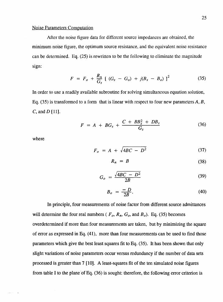
Noise Parameters Computation
After the noise figure data for different source impedances are obtained, the
minimum noise figure, the optimum source resistance, and the equivalent noise resistance
can be determined. Eq. (25) is rewritten to be the following to eliminate the magnitude
sign:
F = Fo + ~: [ (Gs - Go) + j(Bs - B0 ) ]2 (35)
In order to use a readily available subroutine for solving simultaneous equation solution,
Eq. (35) is transformed to a form that is linear with respect to four new parameters A, B,
C, and D [11].
where
F = A + BGs + C + BB'f + DBs Gs
Fo = A + /4BC - D2
Rn = B
Go = J4BC - D2 2B
Bo = -D 2B
(36)
(37)
(38)
(39)
(40)
In principle, four measurements of noise factor from different source admittances
will determine the four real numbers ( F0 , Rn, G0 , and B0 ). Eq. (35) becomes
overdetermined if more than four measurements are taken, but by minimizing the square
of error as expressed in Eq. (41), more than four measurements can be used to find those
parameters which give the best least squares fit to Eq. (35). It has been shown that only
slight variations of noise parameters occur versus redundancy if the number of data sets
processed is greater than 7 [10]. A least-squares fit of the ten simulated noise figures
from table I to the plane ·of Eq. (36) is sought therefore, the following error criterion is

26
established [9]:
[
2 n B2 1 · C DB·
e = - ~ W· A + B (G· + - 1
) +- + - 1
- F·] (41) 2 L ' ' G· G. G. ' i= 1 l l l
where W; is the weighting factor to be used if certain data are known to be less reliable
than the average. In this simulation, each measurement has the same reliability, therefore
10:
I W; = 1. Then: i= 1
oe oA
10 10
= L W; p = LP = 0 i=:=1 i=1
oe oB
1o ( B~) 10 ( B~) = L W; G; + c. p = L G; + c. p = 0
i=l l i=1 l
where
oe oD
oe oc
10 10
= "' w. _e_ = "' _e_ = 0 L z G· L G. i= 1 l i= 1 l
10 B. 10 B. = "' w. - 1
p = "' - 1 p = 0 L ' G. L G·
i=1 l i=1 l
[ ( B~) c DB. ] P = A + B G; + -' + - + -' - F; G; G; G;
(42)
(43)
(44)
(45)
(46)
The coefficient matrix of the four linear equations is established from Eq. (42) through
Eq. (45):

27
10 ( B2) 10 10 B· 10 I G; +d. I d. Ic~.
i= 1 l i= 1 l i= 1 l
10 ( B2) 10 ( B2r 10 ( B2) 10 B~ I Gi+ c. I Gi +c. I 1+-' IB·+-' G? ' G? i= 1 l i= 1 l i= 1 l i= 1 l
10 10 ( B2) 10 w I (47)
I d. I 1+-' Id? I~; G? i= 1 l i= 1 l i= 1 l i= 1 l
10 B. 10 B~ 10 B. 10 (Bi)2 I a'. IB·+-' I a? I G· ' G?
i= 1 l i= 1 l i= 1 l i= 1 l
By inspection of this matrix, some values of the source admittance Ys can be
recognized which can cause the matrix to become singular. Some of these values are the
one for which a column (row) is proportional to another one or can be obtained as a
linear combination of the other ones. The values of such source admittance are listed
earlier in Eq. (26) to Eq. (31).
A Pascal program is written to process the noise data. The matrix Eq. (47) is
solved by using a subroutine available from "Numerical Recipes Example Book" [12]. A
complete description and a listing of the entire program are included in Appendix C. The
N16 and G 14V102 are simulated under the same conditions for comparison. These data
are then processed by the developed Pascal program. Table IT shows the noise
parameters for the N16 and G14V102 transistors with V8E = 0.8V, V CE = 4Vat
f = 1GHz.

N16
TABLE II
NOISE PARAMETERS OF N16 AND G14V102 TRANSISTORS
Fo Rn Go Bo
dB ohms mmhos mmhos
2.25 42.67 6.31 -1.66
G14V102 2.34 21.32 13.12 -3.43
NOISE FIGURE CIRCLES
As stated previously, the noise figure of a two port network is given by
Rn 2 F = Fo + Gs I Ys - Yo I
To plot noise figures on a Smith chart, Ys and Y0 are expressed in terms of reflection
coefficients Fs and F0 , which are:
and
Ys = 1 - Fs 1 + Fs
Yo = 1
Substituting Eq. (49) and Eq. (50) into Eq. (48) results in the following relation:
F = F0
+ 4Rn I Fs - F0 12
( 1 - I Fs 12 ) I 1 + Fo 12
28
(48)
(49)
(50)
(51)
This equation can be used to design Fs for a given noise figure. To determine a family of
noise figure circles, an intermediate noise figure parameter, N;, is defined [1].

N· -l
=
2 I Fs- Fo I
1 -I Fs 12
p.- F l 0
4Rn/Zo I 1 +To 12
Eq. (52) is then transformed to:
I Fo 12 =
Fs- 1 + Ni
2 N?- + Ni ( 1 - ITo I ) l
(1 + Ni)2
Eq. (54) is recognized as a family of circles with Ni as a parameter. The center and
radius of the circle can be found from:
and
Cpi = Fo -
1 + Ni
R = 1 j 2 2 F; 1 + N. Ni + Ni (1 - IFol ) l
29
(52)
(53)
(54)
(55)
(56)
Eq. (53), Eq. (55), and Eq. (56) show that when Fi = Fo, then Ni = 0, Cpo = Fo, and
Rp0
= 0. That is, the center of the F0 circle is located at F0 with zero radius. From
Eq. (55), the centers of the other noise figure circles are located along the r 0 vector.
The developed Pascal program, which is also used to calculate noise parameters,
calculates the constant noise figure circles (with an increment of 0.5 dB from the
minimum noise figure). A set of constant noise figure circles for the N16 is shown in
Fig. 12. This plot gives information about the noise figure of the device for different
source impedances at 1GHz. A F; dB noise figure circle on the plot specifies the values
of source impedance at which the device will produce a noise figure of F; . This set of
curves show that the minimum noise figure, F 0 = 2.25 dB_ is obtained when
Fs = Fo = 0.52L 10.6°, and at point A, Fs = 0.31 L80° produces F; = 3.25 dB.

30
One point of interest is on the center of the Smith chart, which corresponds to a source
impedance of 50Q. The noise figure at this point is what we can have if the device is put
into a 50Q environment without any tuning circuitry at the input ports.

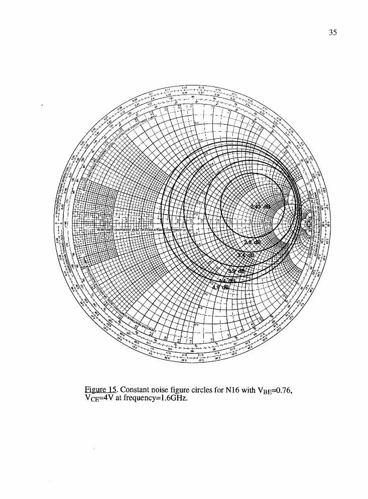
Figure 12. Constant noise figure circles for N16 with VBE = 0.8V, VeE= 4V at Frequency=lGHz.
31

32
COMPARISON
, From the data obtained, the equivalent noise resistance (Rn) of the G14V102 is
smaller than the one of the N 16. This is verified by wider spacing of noise figure circles
of the G 14V102 as compare to the ones of the N16 (Fig. 13 vs. Fig. 14, Fig. 15 vs. Fig.
16). The lower of Rn will result in reduced sensitivity of the noise figure to changes in
source impedance. Therefore, a circuit designer can have more freedom on choosing
source impedances for better power gain and/or better input matching for a given noise
figure.

££
·zHW006=A~u~nb~UJ lU Av=3J A 'A9CQ=3HA ql!M. 91N lOJ S~l~l!~ ~JniJy ~S!OU lUUlSUO:) ·£1 ~Jn~t~

Figure 14. Constant noise figure circles for G14V102 with VBE=0.76V, V cE=4 V at frequency=900MHz.
34
·zHo9·l=A~ugnbgJJ lU Av=3:::>A '9CQ=3HA lll!M 91N JOJ sg1~11~ gJn~y gs10u lUUlSUOJ ·~1 gJn~!d

9£
·zHo9·l=A~u~nb~Jti l~ At=3J A 'A9L·o=3HA ql!M zo 1 A v 1 o JOJ s~I~J!~ ~Jn~u ~s!ou lUUlsuo;) ·g I ~Jn~!ti

CHAPTER IV
GAIN MEASUREMENT
In this chapter, the gain and stability of the bipolar transistors in terms of
s-parameters will be investigated. A procedure for extracting s-parameters from SPICE
is presented. Finally, a comparison between the simulated and measured s-parameter
data will be made.
GAIN AND STABILITY
Stability Criteria
As the operating frequency of the transistor is being pushed upward, the transistor
is more prone to unwanted oscillation due to parasitic elements. From feedback theory,
we know that the input resistance of the common emitter circuit shown in Fig. 17 is
Vs
R.-+ ln Rz
RE
Figure 17. Common emitter amplifier with local series feedback.
R;n = R;~' + (1 + {3) RE, where R;n' is the input resistance of the circuit without the
emitter degeneration resistor RE. There is a multiplying factor of (1 + {3) for RE. This

38
is obvious because the base current is 1 ! f3 times the emitter current. The resistive
parasitic in the emitter, which can be treated the same way as R E in Fig. 17, is being
reflected to the base by the complex f3 as an inductive component at high frequencies.
This inductive reactance and the parasitic capacitance in the transistor may cause the
transistor to oscillate at high frequencies.
The necessary conditions for stability of a two-port device like bipolar transistors,
had been studied by Kurokawa[13], Bodway[14], and Woods[15]. In terms of
s-parameters, they are:
1 Ll 1 = 1 s 11 s 22 - s 12S 21 1 < 1 (57)
and
K = 1 - I s 11 12
- I s 22 12
+ I Ll 12
2 I s 12s 21 I > 1 (58)
Two-port devices that meets the above criteria are unconditionally stable for any positive
source and load impedance.
Stability Circles
To maximize the gain, we must conjugately match the input and the output. For
unconditionally stable two-ports networks there is no unwanted oscillation to worry
about. But for those networks which cannot meet the above stability criteria, we will
have to look at what might happen to the network in terms of stability-will the
amplifier oscillate with certain values of impedance used in the matching process?
In a two-port network, oscillations are possible when either the input or output
port presents a negative resistance, since noise generated in the adjoining network enters
the port, the negative resistance generates more noise rather than dissipating the incident
noise, and some of this generated noise combines with the incoming noise to input more
noise. Negative resistances correspond to the points outside the Smith chart, which

39
imply either I rill I > 1 or I rout I > 1. Therefore, we have the boundary for the input
and output stability circles defined:
I s12s21rz I = I
I rinl = s 11 + 1 - S2f'L (59)
and
- s + -I s12s21rs I - I
I rout I - 22 1 - S 11
Fs (60)
S{)lving for the values of r1 and rs in Eq. (59) and Eq. (60) shows that the solutions for
r 1 and Fs lie on circles [2].
The radius and center of the inpu~ stability circles are:
rs -s 12s21
I s 11 12
- I L1 12
C - ( S 11 - L1 S* ) *
s - 22
I s 11 12
- I L1 12
and the radius and center of the output stability circles are:
where
r = l
Cz -
s12s21
I s22l2
- 1 L1 12
< S22 - L1Si1 )*
I 2 2
S22l - ILl I
L1 = S11S22 - S12S21
(61)
(62)
(63)
(64)
(65)
Having measured the s-parameters of a two-port device at one frequency, Eq. (61) to Eq.
( 64) can be evaluated, and plotted on a Smith chart. Fig. 18 illustrates the graphical
construction of the stability circles where I F;n I -= 1. On one side of the stability
circles boundary, in the r 1 plane, we win have 1 rin 1 < 1 and on the other side
I F;n I > L

40
/ ITinl = 1
Figure 18. Stability circles construction on a Smith chart.
To determine which area represents the stable operating condition, we make
F1 = 0, which is to terminate the output port with a 50.Q load through a 50.Q
transmission line. This represents the point at the center of the Smith chart. Under these
conditions,
I r;n I = I s u I (66)
For N16, the magnitude of S 11 measured is less than unity, therefore, the center of the
Smith chart represents a stable operating point. That is, the shade area on Fig. 19
represents I F;n I < 1 . The same procedure applies for finding the output stability
region.
When the input and output stability circles lie completely outside the Smith chart
the network is called unconditionally stable for all Fs and F1• This comes from the fact
that no matter what positive termination is put at the input or output of the network I F;n I
and I F out I will be always less than unity.
The TEKSPICE script for calculating input and output stability circles based on
Eq. (61) to Eq. (65) is listed in Appendix D.

41
I rinl = 1
I rin I>
I S11 1 < 1
Figure 19. Stability region for rs.
Gain Circles
S-parameters can be used to predict the available power gain of a transistor for
any input termination rs. This available gain is that gain achieved when a transistor is
driven from some source reflection Fs while terminated with a load impedance equal to
Taut (matched output). The available power gain in terms of reflection coefficients is
[1]:
GA
where
2 - (1 - I rs I ) I s 12 1
2 21 2 11- SuFsl (1-1 Foutl)
s12S21Fs Tout = S22 + 1 - S
11Ts
(67)
(68)
Because G A is a function of the source reflection coefficient, constant available power
gain circles can be plotted on a Smith chart together with the constant noise figure
circles, and the trade-off result between gain and noise figure can be analyzed.
For a given gain G A' the radius Ra and the center Ca of the circle can be
calculated using the relations [2] _

Ra =
and
ga = GA -2
I s21 I
C1 = S11 - LlSi2
j 1 - 2K I S12S21 I ga + I s12S21I2g~ I 1 + g a( I S 11 1
2 - I L1 1
2 ) I
C _ gaCi
a - ------~~------1 + ga( I Sul
2 - I L1 1
2 )
42
(69)
(70)
(71)
(72)
For a given G A' the constant available power gain circle can be plotted. All Fs on this
circle produce the gain GA. A TEKSPICE script for calculating the radius and center of
gain circles is given in Appendix E.
S-PARAMETERS FROM TEKSPICE
From the previous discussion, gain and stability circles of a two-port network can
be obtained from manipulation of s-parameters of the network. In addition to noise
figure data, SPICE simulation can provide s-parameters of a two-port network as well.
S-parameters are ratios of incident and reflected wave at the ports of a network. In order
to get s-parameters from TEKSPICE simulation, they need to be calculated in terms of
input and output voltages and currents [16]. For the two-port network shown in Fig. 20,
the input reflection coefficient can be calculated from node voltages:
V1 - Zs / 1 Su = V1 + Zs /1
(73)
= V 1 - (Vs - V 1) (74)
V1 + (Vs - V1)
= 2V1 - Vs (75) Vs
where V1, Vs and S11 are complex variables.

zs = 50Q
--
vl Two-Port
Network V2
Figure 20. Test circuit for obtaining S11 and S21 •
If Vs = 2V L0°, then Eq. (75) is simplified to:
S11 = V1 - 1
For the forward transmission coefficient, the deviation is followed:
V2 - Zz /2 S21 = V
1 + Zs 11
V2 - ( - V2)
- V1 + (Vs - V1)
2V2 = Vs
where V2, Vs and S21 are also complex variables.
If Vs = 2 V L 0°, then S 21 is just simply:
S21 = Vz
Zt = 50Q
For S22 and S 12, the same technique is employed. This time the network is
reversed, as shown in Fig. 21.
43
(76)
(77)
(78)
(79)
(80)

-Zs = 50Q -VI
Two-Port Network
zl = 50Q
v2
--
Figure 21. Test circuit for obtaining S22 and S12•
With V1 = 2 V L 0°, they are:
s22 = v2 - 1
S12 = vl
VI
A TEKSPICE script for perfonning the above arithmetic is listed in detail in
Appendix F.
COMPARISON
44
(81)
(82)
For an N16 with VBE = 0.16V, V CE = 4Vand f = 900MHz, the measured and
simulated s-parameter data are plotted in Fig. 22 to Fig. 29. The simulated data are
based on the device models provided by Tektronix. Those models have been proven to
be representing the actual devices closely by many successful ICs manufactured by
Tektronix. Some deviations between the simulated data and the measured data can be
noticed, (Fig. 23, Fig. 25, and Fig. 29). These are all happening in the phase of the
measured s-parameters. This is traced to a problem with the network analyzer and its
frequency generator. The frequency from the generator is not locked onto the network
analyzer. Even though the frequencies are the same, they are not necessarily in phase.
When the frequencies are matched, measured and simulated data agree with each other,
(Fig. 27). The magnitudes of the measured s-parameters (Fig. 22, Fig. 24, Fig. 26, and
Fig. 28) are in agreement with the simulated data. This proves the method employed to

45
obtain s-parameters from SPICE is valid. To avoid this frequency mismatch problem, a
frequency synthesizer under the control of the network analyzer needs to replace the
frequency sweep generator currently used.
Gain and stability circles for the N16 and the G14V102 are plotted in Fig. 30 and
Fig. 31. Under the conditions V8E = 0.76V, V cE = 4Vat f = 900MHz, these two
transistors can provide similar power gains.
Finally, the gain and noise figure circles are plotted in Fig. 32 and Fig. 33. From
Fig. 32, the N16 will provide a gain of 16dB and a noise figure of 3.5dB with 50.Q
source impedance under the conditions V8E = 0.76V, V CE = 4Vat f = 900MHz,
while a G 14 V 102 will provide about the same gain but witli a superior noise figure of
2.4dB under the same condition, Fig. 33.
sll m 1.1
I 1 . --
s11 s 1 -. ~---· . . ... . .. ... _
900m
800m ~~
-
' -. . . ' .
' ' 100m
600m
500m
. -',~
-, ·',,.~
.
-. .
' . "' . ' ' . ' 400m . -
. 300m . . . I . I . I I I
lOOmeg 1g lOg
freq
Figure 22. Magnitude of Sn for N16.

46
sll m 0
s11 s -20
-40
-60
-80
-100
_-120
-140 lOOmeg lg lOg
freq
Figure 23. Phase of S11 for N16.
sl2_m 180m
160m sl2 5 ·----=-
140m
120m
lOOm
BOrn
60rn
40m
20m
0
100meg 1g lOg
freq
Figure 24. Magnitude of S12 for Nl6.

s12 m --s12 s
s21_rn
s21 s
90
~ ............ 80
70
60
50 I
, 40
30
20
lOOrneg
3.5
3
2.5
2
1.5
1
SO Om lOOrneg
' I I ~' . . ~
~ ~
I
lg
freq
Figure 25. Phase of S12 for N16.
lg
freq
Figure 26. Magnitude of S21 for Nl6.
47
lOg
lOg

s21 m
s21 s
s22 m
s22 s
180~-----------------------r-----------------------,
160
140
-:120
-100
80
60 lOOmeg
~···· ... ~-
T I I I T T I I I I I
lg lOg
freq
Figure 27. Phase of S21 for N16.
1~--~~--~------------~----------------------~
900m
800m
700m ·
48
600m lOOmeg lg lOg
freq
Figure 28. Magnitude of S22 for N16.

oa.:q:
.5ot .5awoot ~~-L-L~--~--~-----4~~~~~~~~~----~sz-
... ... "' ... '
~------------~~-----4----------------------~0Z-.. .. ..
.. ~--------------------~----------------------~St-
6v

0~
'ZHW006=A:>ugnbgJJ 1~ 91N JOJ sgi:>J!:> Al!HQms pm U!~D '0£ ~un~!tl

·zHW006=A~u~nb~lJ re ZO I API D lOJ S~J~l!~ AlH!QtnS prre U!l?D .I£ ~ln~t~I

·zHW006=A~ugnb~UJ 1~ 91N JOJ sg1~11~ g1n1Iu gs1ou p~ 01uo ·z£ jJn~t~

Figure 33. Gain and noise figure circles for G14V102 at frequency=900MHz.
53

CHAPTER V
CONCLUSION
Noise is created by many physical processes which cannot be avoided. Living
with noise means we must be able to measure and predict it. The noise sources in a
bipolar transistor have been identified. At microwave frequencies they are thermal noise
due to base resistance and shot noise from the base and collector currents. The base
resistance consists of two parts. The external base resistance, R bl, is the resistance of the
path between the base contact and the edge of the emitter diffusion. The active base
resistance, R b2, is that resistance between the edge of the emitter and the site within the
base region at which the current is actually flowing. Rb1 can be reduced by decreasing
the separation between the base and the emitter. This method is straightforward, but it is
technology-limited. While the effect of current crowding in the base at high current level
will reduce the effect of Rb2, but more shot noise will be generated by the higher current.
The technique of measuring noise parameters (F min' Rn, G 0 , and B 0 ) of a bipolar
transistor has been presented. This same measurement technique can also be employed
to measure the noise parameters of a general two-port network.
This measurement technique can still be improved. The least-square-fit method is
applied to measure F only. The same method will also need to be applied to the
measurement of G0 , and B0 • All the hardware and software need to be integrated
together. A computer driven tuner will be needed to vary the source impedance for each
noise measurement.

REFERENCE
[1] "S-parameter Design," Hewlett-Packard Application Note 154, Mar. 1990.
[2] Guillermo Gonzalez, Microwave Transistor Amplifiers, Prentice-Hall, New Jersey,. 1984.
[3] P.R. Gray and R. G. Meyer, Analysis and Design of Analog Integrated Circuits, 2nd ed., John Wiley & Sons, New York, 1984.
[4] Z. Y. Chang and M. C. Willy, Low-Noise Wide-Band Amplifiers in Bipolar and CMOS Technologies, Kluwer Academic ~ublishers, Norwell, MA, 1991.
[5] Harry F. Cooke, "Transistor Noise Figure," Solid State Design, pp. 37-42, Feb. 1963.
[6] H. A. Haus et al., "IRE Standards on Methods of Measuring Noise in Linear Twoports, 1959," Proc. IRE, vol. 48, pp. 60-68, Jan. 1960.
[7] H. A. Haus et al., "Representation of Noise in Linear Two ports," Proc. IRE, vol. 48, pp. 69-74, Jan. 1960.
[8] W. Kokyczka, A. Leupp, and M. J. 0. Strutt, "Computer-aided determination of two-port noise parameters (CADON)," Proc. IEEE, vol. 58, pp. 1850-1851, Nov. 1970.
[9] Richard Q. Lane, "The Determination of Device Noise Parameters," Proc. IEEE, vol. 57, pp.1461-1462, Aug. 1969.
[10] G. Garuso and M. Sannino, "Computer-Aided Determination of Microwave Two-port Noise Parameters." IEEE Transactions on Microwave Theory and Techniques, vol. 26, pp. 639-642, Sept. 1978.
[11] H. Fukui, ''The Noise Performance of Microwave Transistors," IEEE Transactions on Electron Devices, vol. 13, pp. 329-341, Mar. 1966.
[12] William Vetterling, Numerical Recipes Example Book (Pascal), Cambridge University Press, New York, 1985.
[13] K. Kurokawa, "Power Waves and the Scattering Matrix," IEEE Transactions on Microwave Theory and Techniques, vol. 13, pp. 194-202, Mar. 1965.

[14] G. E. Bodway, "Two Port Power Flow Analysis Using Generalized Scattering Parameters," Microwave Journal, May 1967.
56
[15] D. Woods, "Reappraisal of the Unconditional Stability Criteria for Active 2-Port Networks in Terms of S Parameters," IEEE Transactions on Circuits and Systems, Feb. 1976.
[16] Ronald W. Kruse, "Microwave Design Using Standard Spice," Microwave Journal, pp. 164-171, Nov. 1988.
[ 17] W. Baechtold and M. J. 0. Strutt, "Noise in Microwave Transistors," IEEE Transactions on Microwave Theory and Techniques, vol. 16, Sept. 1968.
[ 18] H. T. Friis, "Noise Figure of Radio Receivers," Proc. IRE, vol. 32, pp. 419-422, July 1944.
[19] -Richard Q. Lane, "A Microwave Noise and Gain Parameter Test Set," IEEE International Solid-State Circuits Conference, pp. 172-173, 1978.
[20] Neal Silence, "The Smith Chart and Its Usage in RF Design," RF Expo West Proceedings, pp. 1-7, Mar. 1992.
[21] George D. Vendelin and William C. Mueller, "Noise Parameters of Microwave Transistors," Microwave Journal, pp. 177-186, Nov. 1987.
[22] P. H. Smith, ''Transmission Line Calculator," Electronics, vol. 12, pp. 29-31, Jan. 1939.

.LWH:> H.LIWS dO NOI.LV:>I'lddV ONV NOll:>flM.LSNO:>
VXIGN3ddV

58
APPENDIX A
CONSTRUCTION AND APPLICATION OF SMITH CHART
Equations like the one for reflection coefficient, r = Cl- ~)are often used in (Z + )
microwave theory. Since all the values in this equation are complex numbers, the
computations to solve this equation are tedious and "boring". Back in the thirties, Phillip
Smith, a Bell Lab engineer, developed a graphical method for solving this often repeated
equation [22]. In honor of his contribution, the chart is named Smith chart.
CONSTRUCTION OF SMITH CHART
The chart is essentially a mapping between two planes-the Z or impedance plane
and the r or reflection coefficient plane. The actual mechanics of the transformation are
accomplished as follows. Represent impedance Z in rectangular format:
Z = r + jx
Divide the equation for reflection coefficient into its real and imaginary parts:
r = u + jv = (r - 1) + jx
Then separate the real and imaginary parts to obtain
r2 - 1 + x 2 u = ...;.__..;;;;.._;__;,.;.._ (r + 1)2 + x2
v = 2x (r + 1)2 + x2
Eliminating x from these equations yields
(u - _r )2 + v2 = (-1 )2 r + 1 r + 1
(83)
(84)
(85)
(86)
(87)

This equation represents a circle of radius , 1 4 , with its center at u = , r 4 , and
v = 0. From this, a family of circles is obtained that represent a loci of constant
resistance with their centers on the u axis of Fig. 34 and a common point at u = 1 and
Locus of Co~stant, Res1stance '-
r=O•
+v
I I
-- I_. ' '1L_ -~1 "f "1~ 1) '~I
'
u = 1
59
I I I "' ,. _, I c: a + U
Locus of Constant Reactance
\ \
" / "
" 1 /) " I ,-x I \ --1-- / "-- 1 \ ~ I X I
\ I I " I / ........... / ----
Fi~ure 34. Smith chart construction.
v = 0. For a range of r from zero to infinity and x = 0 all circles are contained within a
circle described by a reflection coefficient of magnitude of 1 and variable phase, which is
also the circle for r = 0.
Eliminating r from Eq. (85) and Eq. (86) yield the loci of constant reactance:
2 1 =-)
2 1 ( u - 1) + ( v - x x2 (88)
Again, a family of circles is obtained. However, this time the centers lie along a vertical

line at points of u = 1 and v = ± :}. Since the radii of there circles are ~' they also
have a common point of u = 1 and v = 0.
APPLICATION OF SMITH CHART
A point on a Smith chart simultaneously represents three different things.
60
Depending on the coordinate system used as a reference, they are: reflection coefficient,
impedance, and admittance. For a system with input impedance of Z;n = 100 + 50jQ in
a 50Q environment, the input reflection coefficient and the input admittance can be
directly read from the chart.
Normalize Z;n to 50Q to get Z;n = 2 + lj, and locate this point on the Smith
chart, point A. Draw a line from the center of the chart passed point A and intercept with
the peripheral dial. The distance between the center of the chart and point A is the
magnitude of the reflection coefficient and the angle indicated on the dial is the phase.
For this case F;n = 0.45 L 26.6°. By looking at the admittance circles, the input
admittance is Y;n = 0.4 - 0.2j.
The application of Smith is not limited to obtain the reflection coefficients of a
circuit. It can be used as a graphical aid for impedance transformation, to show the
variation of Z and Y with frequency, to determine the standing wave patterns, et al. For a
detail explanation on the usage of the Smith chart, "Microwave Transistor Amplifiers,"
by Gonzalez [2] is one of the many good references to consult with.

61
~l ~~~ ~~ """ TO'NAROLOAO-• •-TOWAROGENERATOR ";::> if\ '~ •10010 210 to ~ 4 3 2 s 2 1 a 1 e t.• t 2 , 1 1 15 10 1 & 4 3 2 , S'
· ~ ~ 11,'"1' "'' ,\\',","/'/"' "•" '•'•'•"•'•' '"'1'"','/','•',',1" 'I'•'• ,',/, ,•,\,'/,',',1 ~· {!w. ~ ~ "' .. .a JO 20 ts to a e a " .a 2 t t 1 1.1 t.z t.s t.4 1.1 1.1 z .a • s 10 zo x <o ~
~A",co; o t 2 a • 6 e 1 e e to 12 •• 20 ao o 01 02 o... o.e o.a t t 6 2 3 • & s 10 tfi-ot q;:~· · a' :"' 1 og oe 0.1 o.s o.6 o• 03 02 01 0.06 001 oa 1.1 1.2 13 1.4 16 I.e 111819 2 2& a • & IO• Y/ [.,/ I 01 01 07 0.8 05 0.4 03 02 01 0 I 081 08& 0.1 01 07 U M 04 03 02 01 0 ,
CENTER o 01 0.2 03 o.- 01 o.e 0.1 o.e o.g 1 1.1 1.2 u u u u t 7 1.1 u 2 """' '"'" '"' """ '""' """ "" """ """ """ """ "" '""' ""'
ORIGIN
Figure 35. A complete Smith chart.

SNOI~V!il;)!V;) ffiiDDid 3SION
S: XION3ddV

63
APPENDIXB
NOISE FIGURE CALCULATIONS
This TEKSPICE script calculates noise figures for a two-port network described
in the file "device" at various bias conditions. It is divided into four basic blocks. They
are: header block, circuit description block, analysis block, and data processing block. In
order to vary the source impedance, the values of rsource, and inductance will need to be
change according to the rules specified in Chapter II under the topic "source impedance
selection".
;---------------------------------------------------------------; Script header to define variables, and to specify location of ; device library. ;---------------------------------------------------------------libpath -/picuslib clear rsource=50 inductance=14.9n
path for device library clear all variables
specify source impedance
;---------------------------------------------------------------; Circuit description. ;---------------------------------------------------------------circuit rsource vin inductance read device ; file "device" contains the DUT v1 1 0 v:ac=1 ; AC signal source rs 1 4 r:r=rsource ; Source impedance inpad 5 0 pad ; connecting pad at the base 11 4 2 l:l=inductance ; input matching element cin 2 5 c:c=1 ; DC blocking capacitor at the input lin 5 6 1:1=1 ; RF choke vbias 6 0 v:dc=vin ; VBE for the device outpad 7 0 pad ; connecting pad at the collector cout 7 3 c:c=1 ; DC blocking capacitor at the output lout 7 8 1:1=1 ; RF choke vee 8 0 v:dc=4 ; VeE for the device rload 100 0 3 100 ccvs:p1=50; noiseless load resistor endc ; end of circuit description

64
;---------------------------------------------------------------; Noise analysis for various bias conditions. ; V8 E starts at 750rnV and ends at 850rnV. ;---------------------------------------------------------------var sweep vin : 0.75 0.85 0.01
ac analysis freq :lrneg lOg 5 type=dec noise v(3) vl
endac endvar
;---------------------------------------------------------------Calculation for device noise figure.
v2 NF = 10 * log 10 4KTR
;---------------------------------------------------------------
nf=10*log10((rnag(inoise)A2)/(4*1.38e-23*300*rsource)) freq=lg plot reduce(nf,freq) :title="Noise Figure vs. VBE for Nl6 at lGHz"

SNOI.LV1il:l1V:l
S31:l"MI:l ti"MilDI.:I 3SION CINV S"M3~3WV"MVd 3SION
:lXION3ddV

APPENDIXC
NOISE PARAMETERS AND NOISE FIGURE CIRCLES
CALCULATIONS
This Pascal program uses the least-square-fit method and the square matrix
inversion subroutine from "Numerical Recipes Example Book" [ 12] to calculate noise
parameters (F0 , Rn, B 0 , and G0 ) from noise figure measurements.
66
The input file contains the real part and imaginary part of the source impedance·
and the noise figure measured for that source impedance. It is in the form of
Rs, Xs, NF. The program is written to accept a maximum of 25 sets of data.
140 50 37.5 20 70 25 16 70 60 40
50 -17.5 -10 -2 6. 25
70 35 10
5 15 12.5
2.004 3.641 4.210 6.157 2.594 4.836 6.396 2.861 3.045 3.856
The following is a sample output from the noise parameters calculation program.
It consists of two sections. The first part gives the four noise parameters NF min' Rn, G0 ,
and B 0 • The second part gives the coordinates of noise figure circles on a Smith chart in
0.5 dB increment from the minimum noise figure.
NFmin = 1.89 dB Rn = 53.88 ohms Go = 4.13 mmhos Bo = -1.94 mmhos
NF = 1.89 dB Center = 0.6602 @ 11.54 Radius = 0.0000 NF = 2.39 dB Center = 0.5898 @ 11.54 Radius = 0.2551 NF = 2.89 dB Center = 0.5268 @ 11.54 Radius = 0.3630 NF = 3.39 dB Center = 0.4704 @ 11.54 Radius = 0.4452

67
NF = 3.89 dB Center = 0.4200 @ 11.54 Radius = 0.5128 NF = 4.39 dB Center = 0.3749 @ 11.54 Radius = 0.5703 NF = 4.89 dB Center = 0.3346 @ 11.54 Radius = 0.6199 NF = 5.39 dB Center = 0.2986 @ 11.54 Radius = 0.6632 NF = 5.89 dB Center = 0.2664 @ 11.54 Radius= 0.7011 NF = 6.39 dB Center = 0.2376 @ 11.54 Radius= 0.7346 NF = 6.89 dB Center = 0.2120 @ 11.54 Radius = 0.7641
The followings are the block diagram and the complete listing of the Pascal
program developed for calculating noise parameters for a two-port network.
Main
I I I I I I I
Initialize readfile Combinedata Creatematrix Invert Multiply
Cal noise Noiseci rcle
Fi~ure 36. Flow chart for noise parameters calculation.
{**************************************************************} { This program calculates the least-square-fit noise } { figure from measurement data to obtain noise } { parameters for a two port device. Base on these } { calculated data, the program outputs a family of } { coordinates for noise figure circles to be plotted } { on a Smith chart. } {**************************************************************} program noisecal (input,output,datafile);
const pi=3.14159265; {* define number of sets of data point *} maxdatapoints=25; {* There are total of 4 noise parameters *} n=4;
type {* 4x4 matrix for 4 unknown *} squmatrix=array [1 .. n,1 .. n] of real; {* 1x4 matrix *} abcdmatrix=array [1 .. n] of real; {* matrix for raw datas *}

measurematrix=array [1 .. maxdatapoints] of real; {* data points for NF circles *} circledata=array [1 .. 10] of real;
var num, i : integer; fmin, rn, bopt, gopt, maggammao, phasegammao gs, bs, f, x, y, z : measurematrix; a, ai : squmatrix; b, result : abcdmatrix; center, radius : circledata; datafile : text;
68
real;
{*------------------------------------------------------------*} {* Calculates the magnitude of a complex number. *} {*------------------------------------------------------------*} function mag (realnum, imagnum : real) : real; begin
mag:= sqrt(realnum*realnum+imagnum*imagnum); end; {* of function *}
{*------------------------------------------------------------*} {* Calculates the phase of a complex number. *} {*------------------------------------------------------------*} function phase (realnum, imagnum : real) : real; var
temp : real; begin
if (realnum = 0) and (imagnum = 0) then
temp := 0; if (realnum = 0) and (imagnum <> 0)
then if ( imagnum > 0)
then temp : = pi/2
else temp := (-1)*pi/2;
if (realnum <> 0) and (imagnum = 0) then
if (realnum > 0) then
temp := 0 else
temp : = pi; if (realnum <> 0) and (imagnum <> 0)
then begin
temp:= arctan(imagnum/realnum); if (realnum < 0)
then temp := temp +pi;
end; phase := temp;

69
end; {* of function *}
{*------------------------------------------------------------*} {* Calculates the real component of a complex number. *} {*------------------------------------------------------------*} function realpart (mag1, phase1 : real) : real; begin
realpart := mag1 * cos(phase1); end; {* of function *}
{*------------------------------------------------------------*} {* Calculates the imaginary part of a complex number. *} {*------------------------------------------------------------*} function imagpart (mag1, imag1 :real) :real; begin
imagpart := mag1 * sin(imag1); end; {* of function *}
{*------------------------------------------------------------*} {* Initialize matrix for later use. *} {*------------------------------------------------------------*} procedure initialize (var a : squmatrix;
var b: abcdmatrix); var
i, j : integer; begin {* initialize *}
for i := 1 to n do begin
for j := 1 to n do a[i,j] := 0;
b[i] := 0; end;
end; {* of initialize *}
{*------------------------------------------------------------*} {* Reads in resistance, reactance, and noise figure from *} {* data file "datafile". Puts the data into arrays. *} {*------------------------------------------------------------*} procedure readfile (var gs, bs, f : measurematrix;
var num: integer); var
i : integer; re, im, nf : real;
begin {* readfile *} reset (datafile); i : = 0; while not eof(datafile) do
begin i := i+1; readln (datafile,re,im,nf); f [ i ] : = exp ( ( n f I 1 0 ) * 1 n ( 1 0 ) ) ; gs [ i J : = re/ ( re*re+im* im) ; bs(i] := (-1) *im/ (re*re+im*im);

end; num : = i;
end; {* of readfile *}
70
{*------------------------------------------------------------*} {* Puts the data into the form specified in paper *} {*------------------------------------------------------------*} procedure cornbinedata {var x, y, z : measurematrix;
gs, bs : measurematrix; nurn: integer);
var i : integer;
begin {* cornbinedata *} for i := 1 to nurn do
begin x[i] := gs[i]+{bs(i]*bs(i])/gs(i]; y[i] := 1/gs[i]; z[i] := bs[i]/gs[i];
end; end; {* of cornbinedata *}
{*------------------------------------------------------------*} {* Creates the two matrixs to solve the four noise *} {* parameters. *} {*------------------------------------------------------------*} procedure creatematrix {x, y, z, f : measurematrix;
num : integer;
var i, j : integer;
begin {* creatematrix *} { Calculating a matrix }
a[1,1] := nurn; for j := 1 to nurn do
begin
var a:squmatrix; var b:abcdrnatrix);
a[2,1] := x[j] + a[2,1]; a[3,1] := y[j] + a[3,1]; a[4,1] := z[j] + a[4,1]; a[2,2] := x[j]*x[j] + a[2,2]; a [ 3 , 3 J : = y [ j ] *y [ j J + a [ 3 , 3 J ; a[4,4] := z[j]*z[j] + a[4,4]; a [ 3 , 2 ] : = x [ j J *y [ j J + a [ 3 , 2 J ; a[4,2] := x[j]*z[j] + a[4,2]; a[3,4] := y[j]*z[j] + a[3,4];
end; for i := 2 to 4 do
a[1,i] := a[i,l]; a[2,3] := a[3,2]; a[2,4] := a[4,2];

a[4,3] := a[3,4]; { Calculating b matrix }
for j := 1 to num do begin
b[1] := f[j] + b[1]; b[2] := x[j]*f[j] + b[2]; b[3] := y[j]*f[j] + b[3]; b[4] := z[j]*f[j] + b[4];
end; end; {* creatematrix *}
71
{*------------------------------------------------------------*} {* Inverts the square matrix. *} {*------------------------------------------------------------*} procedure invert (a: squmatrix; var ai: squmatrix);
var big, dum, pivinv : real; i, icol, irow, j, k, 1, 11 : integer; ipiv, indxc, indxr: array[1 .. n] of integer;
begin {* invert *} for j := 1 to n do
ipi v [ j] : = 0 i for i := 1 to n do
begin big := 0.0; for j := 1 ton do
if (ipiv[j] <> 1) then
matrix');
for k := 1 ton do if (ipiv[k] = 0)
then
else
if (abs(a[j,k]) >=big) then
begin big:= abs(a[j,k]); irow := j; icol := k
end
if (ipiv[k] > 1) then
begin writeln('pause 1 in GAUSSJ- singular
readln end;
ipiv[icol] := ipiv[icol]+1; if (irow <> icol)
then for 1 := 1 to n do
begin dum:= a[irow,l];

a [ irow, 1] : = a [ icol, 1] ; a[icol,l] :=dum
end; indxr(i] := irow; indxc[i] := icol; if (a[icol,icol] = 0.0)
then begin
writeln('pause 2 in GAUSSJ- singular matrix'); readln
end; pivinv := 1.0/a[icol,icol]; a[icol,icol] := 1.0; for 1 := 1 ton do
a [ icol, 1] : = a [ icol, 1] *pi vinv; for 11 := 1 to n do
end;
if (11 <> icol) then
begin dum:= a[ll,icol]; a[ll,icol] := 0.0; for 1 := 1 to n do
a[ll,l] := a[ll,l]-a[icol,l]*dum; end;
for 1 := n downto 1 do begin
if (indxr[l] <> indxc[l]) then
for k := 1 to n do begin
dum:= a[k,indxr[l]]; a [ k, indxr [ 1] J : = a [ k, indxc [ 1] ] ; a[k,indxc[l]] :=dum
end; end;
for i := 1 to n do for j := 1 ton do
ai[i,j] := a[i,j]; end; {* of invert *}
{*------------------------------------------------------------*} {* Multiplies two matrixs *} {*------------------------------------------------------------*} procedure multiply (ai : squmatrix;
b : abcdmatrix;
var i, j : integer;
begin {* multiply *} for i := 1 to n do
begin
var result : abcdmatrix) ;
72

result[i] :=0; for j := 1 to n do
begin
end;
result(i] := result(i]+ai[j,i]*b[j]; end;
end; {* of multiply *}
73
{*------------------------------------------------------------*} {* Calculates the four noise parameters. *} {*------------------------------------------------------------*} procedure calnoise (result : abcdmatrix;
var fmin, rn, gopt, bopt :real};
var a, b, c, d : real;
begin {* calnoise *} a:= result[1]; b := result[2]; c := result[3]; d := result[4]; fmin :=a+ sqrt(4*b*c-d*d); if fmin <= 0 then
begin writeln ('fmin <= 0; take more data point'); readln;
end; rn : = b; gopt := (sqrt(4*b*c-d*d))/(2*b); bopt := (-1)*d/(2*b);
end; {* of calnoise *}
{*------------------------------------------------------------*} {* Calculates the centers and radii of noise figure *} {* circles in 0.5dB increments. *} {*------------------------------------------------------------*} procedure noisecircle (fmin,rn,maggammao,phasegammao : real;
var center,radius : circledata};
var i : integer; temp, ni, reg, img real;
begin reg:= realpart(maggarnmao,phasegammao); img := imagpart(maggammao,phasegarnmao); temp:= mag(1+reg,img)*mag(1+reg,img); for i := 1 to 10 do
begin ni := (fmin*(exp(0.05*i*ln(10))-1))/(4*rn/50)*temp; center[i] := maggarnmao/(1+ni); radius[i] :=
1/(1+ni)*sqrt(ni*ni+ni*(l-maggarnmao*maggarnmao));

74
end; end; {* of noisecircle *}
{*============================================================*} begin {* main *}
initialize (a, b); readfile (gs, bs, f, num); combinedata (x, y, z, gs, bs, num); creatematrix (x, y, z, f, num, a, b);
{Solve equation} invert (a, ai); multiply{ai, b, result); calnoise{result, fmin, rn, gopt, bopt); magganunao :=
mag((1-gopt*50), (-bopt*50))/mag((1+gopt*50), (bopt*50)); phaseganunao
:=(phase((1-gopt*50), (-bopt*50))-phase( (l+gopt*50), (bopt*50))); noisecircle(fmin,rn,maggarnmao,phaseganunao,center,radius); fmin := 10*ln(fmin)/ln(10); writeln {'NFmin = ',fmin:5:2,' dB'); writeln ('Rn = ',rn:5:2,' ohms'); writeln ('Go = ',gopt*1000:5:2,' nunhos'); writeln ('Bo = ',bopt*1000:5:2,' nunhos'); writeln; write ('NF = ',fmin:5:2,' dB',' Center= ',maggammao:6:4); writeln ('@ ',phasegammao*180/pi:5:2,' Radius= 0.0000'); for i := 1 to 10 do
begin write ('NF = ',fmin+(i/2) :5:2,' dB ',' Center=
' , center [ i ] : 6 : 4 ) ; writeln {' @ ',phasegammao*180/pi:5:2,' Radius=
',radius[i] :6:4); end;
end. {* of main *} {*=======================END OF PROGRAM=======================*}

SNOI~VJ.i1dWOJ S3'1J"MIJ lll'liHV~S
OXION3ddV

76
APPENDIXD
STABILITY CIRCLES COMPUTATIONS
Stability Criteria
This TEKSPICE script calculates and prints out the two stability criteria, Eq. (89)
and Eq. (90), from s-parameters of a two-port network.
1 L1 1 = I s 11 s 22 - s 12s 21 I < 1
1 - I Sn 12
- I s22l2
+ 1 L1 12
K = ----~----=-------2 I s12s21l
(89)
> 1 (90)
;--------------------------------------------------------------; Clears all variables. ;--------------------------------------------------------------clear
;--------------------------------------------------------------; Reads ins-parameter data from file "sdata". ;--------------------------------------------------------------probe sllre_s,sllim_s,sl2re_s,s12im_s,s21re_s,s21im_s,s22re_s,s22im_s: f=sdata format=plotdt
sll_s=cmplx(sllre_s,sllim_s) sl2_s=cmplx(s12re_s,s12im_s) s21_s=cmplx(s21re_s,s21im_s) s22_s=cmplx{s22re_s,s22irn_s)
;--------------------------------------------------------------; Calculates the two stability criteria ;--------------------------------------------------------------delta=sll_s*s22_s-s12_s*s21_s
k=(l-(rnag(sll_s)A2)-{mag(s22_s)A2)+(mag{delta)A2))/{2*mag{sl2_s* s21_s}}
;--------------------------------------------------------------; Writes the results into files "delta" and "kfactor" for ; stabilty circles computation, and displays them on the ; terminal ;--------------------------------------------------------------delta_re=real(delta)

delta_im=imag(delta)
print delta_re, delta_im:f=delta format=plotdt print k:f=kfactor format=plotdt print k, mag(delta)
Stability Circles Computation
77
This TEKSPICE script calculates the input and output stability circles from
s-parameters of a two-port network. The radius and center of the input stability circles
are:
rs = I s 11 1
2 - I L1 1
2 s12S21 (91)
C - ( S 11 - Ll S* ) *
s - 22
I s 11 12
- I L1 I (92)
and the radius and center of the output stability circles are:
'1 = 1 S12S21
I s2212 - I Ll 12 (93)
C - ( S 22 - L1 S* ) * z- 11
I s22l2
- 1 Ll 12
(94)
;---------------------------------------------------------------; Clears all variables. ;---------------------------------------------------------------clear
;--------------------------------------------------------------; Reads ins-parameter data from file "sdata". ;--------------------------------------------------------------probe sllre_s,sllim_s,s12re_s,s12im_s,s21re_s,s21im_s,s22re_s,s22im_s: f=sdata format=plotdt
sll_s=cmplx(sllre_s,sllim_s) s12_s=cmplx(s12re_s,s12im_s) s21_s=cmplx(s21re_s,s21im_s) s22_s=cmplx(s22re_s,s22im_s)
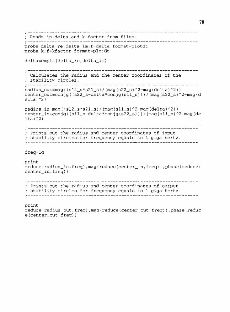
;--------------------------------------------------------------; Reads in delta and k-factor from files. ;--------------------------------------------------------------probe delta_re,delta_irn:f=delta forrnat=plotdt probe k:f=kfactor forrnat=plotdt
delta=cmplx(delta_re,delta_im)
;--------------------------------------------------------------; Calculates the radius and the center coordinates of the ; stability circles. ;--------------------------------------------------------------
78
radius_out=rnag((sl2_s*s2l_s)/(mag(s22_s)A2-mag(delta)A2)} center_out=conjg((s22_s-delta*conjg(sll_s)}}/(mag(s22_s)A2-mag(d elta}A2)
radius_in=mag((sl2_s*s2l_s}/(rnag(sl1_s)A2-mag(delta)A2)} center_in=conjg((s11_s-delta*conjg(s22_s) })/(mag(sl1_s)A2-mag(de lta}A2)
;--------------------------------------------------------------; Prints out the radius and center coordinates of input ; stability circles for frequency equals to 1 giga hertz. ;--------------------------------------------------------------
freq=lg
print reduce(radius_in,freq),rnag(reduce(center_in,freq}} ,phase(reduce( center_in, freq) )
;--------------------------------------------------------------; Prints out the radius and center coordinates of output ; stability circles for frequency equals to 1 giga hertz. ;--------------------------------------------------------------
print reduce(radius_out,freq) ,mag(reduce(center_out,freq)},phase(reduc e(center_out,freq))

NOIJ.VlildWOJ S'31J'MIJ NIVD
'3 XION'3ddV

APPENDIXE
GAIN CIRCLES COMPUTATION
This TEKSPICE script calculates the center and radius of a gain circle from the
s-parameters of a two-port network according to the following equations:
80
ga = GA I s21 12
(95)
and
C1 = Su - Lls;2
j 1 - 2K I S12S21 I ga + I s12s21l2g~ Ra = 2 2 I 11 + ga( I S11 I - 1 Ll 1 )
Ca = ------------~ga~C~i~-----------1 + ga( I Sul
2 - I Ll 1
2 )
(96)
(97)
(98)
;--------------------------------------------------------------; Reads ins-parameter data from file "sdata". ;--------------------------------------------------------------probe sllre_s,sllim_s,s12re_s,s12im_s,s21re_s,s21im_s,s22re_s,s22im_s: f=sdata format=plotdt
sll_s=cmplx(sllre_s,sllim_s) s12_s=cmplx(s12re_s,s12im_s) s21_s=cmplx(s21re_s,s21im_s) s22_s=cmplx(s22re_s,s22im_s)
;--------------------------------------------------------------; Reads in delta and k-factor from files. ;--------------------------------------------------------------probe delta_re,delta_im:f=delta format=plotdt probe k:f=kfactor format=plotdt
delta=cmplx(delta_re,delta_im) glinear=lOA(ga/10)

gain=glinear/(mag(s21_s)A2)
;--------------------------------------------------------------; Calculates the radius and the center coordinate of a gain ; circle. ;--------------------------------------------------------------c=sll_s-delta*(conjg(s22_s))
81
denom=l+gain*(mag(sll_s)A2-mag(delta)A2) radius=((l-2*k*gain*mag(s12_s*s21_s)+gainA2*mag(s12_s*s21_s)A2)A 0.5)/denom center=gain*conjg(c)/denom
;--------------------------------------------------------------; Displays the radius and center coordinate for a gain circle on ; the termial. ;--------------------------------------------------------------freq=lg print reduce(radius,freq) reduce(mag(center),freq)

NOI~:>VID.X3 S"M3~3:WVWd-S
dXION3ddV

APPENDIXF
S-PARAMETERS EXTRACTION
This TEKSPICE script provides the s-parameters for a two-port network. The
calculation of s-parameters from node voltages is derived in the text. The valus of the
source voltage in AC analysis is arbitrary with respect to s-parameter calculation. The
calculation is simplified by using a 2V AC source.
;--------------------------------------------------------------; Sets up path for device library, clears variables. ;--------------------------------------------------------------libpath -/picuslib clear autoprobe=on vsource=O
;--------------------------------------------------------------; Reads in bias condition. ;--------------------------------------------------------------circuit vsource vin vsupply read bias_pt
;--------------------------------------------------------------; Defines a two-port network. ;--------------------------------------------------------------;read in from device file read device lb 5 6 1:1=1 cin 2 5 c:c=1 inpad 5 0 pad vee 8 0 v:dc=vsupply outpad 7 0 pad lc 7 8 1:1=1 cout 7 3 c:c=1 v1 1 0 v:ac=2-vsource v2 4 0 v:ac=vsource r1 1 2 r:r=50 r2 3 4 r:r=50 endc
83

·--------------------------------------------------------------, ; Starts analysis. ;--------------------------------------------------------------var sweep vsource : 0 2 2
ac analysis freq :125meg 16g 3 type=oct endac
endvar
;--------------------------------------------------------------; Extracts s-parameters. ;--------------------------------------------------------------vsource=O s2l_s=reduce(v(3) ,vsource) sll_s=reduce((v(2)-l) ,vsource) vsource=2 sl2_s=reduce(v(2) ,vsource) s22_s=reduce((v(3)-l) ,vsource)
sllre_s=real(sll_s) sllim_s=imag(sll_s) sl2re_s=real(sl2_s) sl2im_s=imag(sl2_s) s2lre_s=real(s2l_s) s2lim_s=imag(s2l_s) s22re_s=real(s22_s) s22im_s=imag(s22_s)
print sllre_s,sllim_s,sl2re_s,sl2im_s,s21re_s,s21im_s,s22re_s,s22im_s :f=sdata format=plotdt
84