Embed Size (px)
Citation preview
1
Measurements on a Multiband R2Pro Low-Noise Amplifier System—Part 2
Gary W. Johnson, WB9JPS
February 19, 2007
1. Introduction Part two of this report discusses the addition of a buffer amplifier to a manually-switched, five-band, low-noise amplifier (LNA) for the HF amateur bands. You should read part one first. The objective here is to improve output return loss that is otherwise problematic in a multiband front-end for a direct-conversion receiver such as the R2Pro1. A straightforward solution is the addition of a buffer amplifier after the LNA, and an attenuator to maximize return loss. Since there are many candidate amplifiers, I will present some results on several reasonable types and gain configurations. More importantly, I made a series of measurements with my own version of the R2Pro to see what kind of performance tradeoffs might be available among the various combinations of amplifiers and attenuation levels.
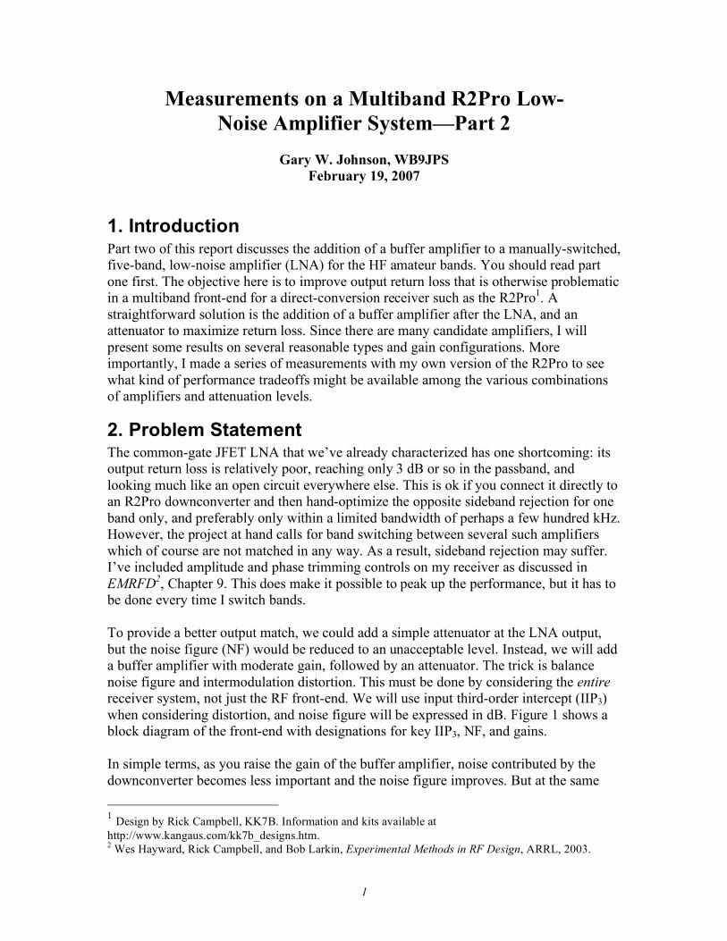
2. Problem Statement The common-gate JFET LNA that we’ve already characterized has one shortcoming: its output return loss is relatively poor, reaching only 3 dB or so in the passband, and looking much like an open circuit everywhere else. This is ok if you connect it directly to an R2Pro downconverter and then hand-optimize the opposite sideband rejection for one band only, and preferably only within a limited bandwidth of perhaps a few hundred kHz. However, the project at hand calls for band switching between several such amplifiers which of course are not matched in any way. As a result, sideband rejection may suffer. I’ve included amplitude and phase trimming controls on my receiver as discussed in EMRFD2, Chapter 9. This does make it possible to peak up the performance, but it has to be done every time I switch bands. To provide a better output match, we could add a simple attenuator at the LNA output, but the noise figure (NF) would be reduced to an unacceptable level. Instead, we will add a buffer amplifier with moderate gain, followed by an attenuator. The trick is balance noise figure and intermodulation distortion. This must be done by considering the entire receiver system, not just the RF front-end. We will use input third-order intercept (IIP3) when considering distortion, and noise figure will be expressed in dB. Figure 1 shows a block diagram of the front-end with designations for key IIP3, NF, and gains. In simple terms, as you raise the gain of the buffer amplifier, noise contributed by the downconverter becomes less important and the noise figure improves. But at the same
1 Design by Rick Campbell, KK7B. Information and kits available at http://www.kangaus.com/kk7b_designs.htm. 2 Wes Hayward, Rick Campbell, and Bob Larkin, Experimental Methods in RF Design, ARRL, 2003.
2
time, the downconverter will now overload with weaker signals, thus the IIP3 is reduced. We will try to choose the best amplifier we can, but in the end, it’s a tradeoff, as you will see. Appendix A includes some of the basic math behind intercept and noise figure calculations. Also see the ARRL Handbook and of course EMRFD.
Figure 1. Block diagram of the RF front-end.
Information we will need is: LNA performance (IIP3 and NF); available in Part I of this report Candidate buffer amplifier designs Amplifier performance data (IIP3, NF, and output return loss) R2Pro performance data, from the downconverter forward (IIP3 and NF) Once we have all of that, optimization is possible, on paper. You will still be able to make your own tradeoffs. In fact, some receivers like the Elecraft K2 have an RF amplifier stage exactly like the one we’re talking about that you can switch in or out. The switch is even labeled High Intercept / Low Noise.
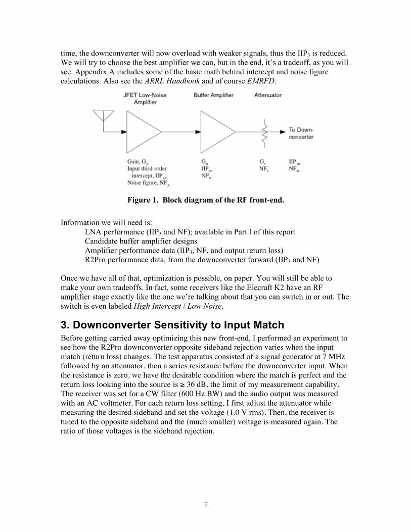
3. Downconverter Sensitivity to Input Match Before getting carried away optimizing this new front-end, I performed an experiment to see how the R2Pro downconverter opposite sideband rejection varies when the input match (return loss) changes. The test apparatus consisted of a signal generator at 7 MHz followed by an attenuator, then a series resistance before the downconverter input. When the resistance is zero, we have the desirable condition where the match is perfect and the return loss looking into the source is ≥ 36 dB, the limit of my measurement capability. The receiver was set for a CW filter (600 Hz BW) and the audio output was measured with an AC voltmeter. For each return loss setting, I first adjust the attenuator while measuring the desired sideband and set the voltage (1.0 V rms). Then, the receiver is tuned to the opposite sideband and the (much smaller) voltage is measured again. The ratio of those voltages is the sideband rejection.
3
With the input matched, gain and phase are alternately adjusted for the best null, which was very good indeed: 75 dB3. Rejection was then measured as each of the various resistors was installed (100, 300, 1K, 3K, and also a 30 pF capacitor). I did listen to the signal on the opposite sideband to check for odd sounds that might indicate distortion or anything unexpected. Some faint harmonics were audible, barely above the noise, when the null was very deep. Otherwise, it was very clean. Figure 2 shows the results. The upper curve shows the variation with the receiver trimmed for the best null. This is really good performance, even when the return loss was very bad. Another reality check was performed to simulate what happens when the receiver does not have the phase trim, which is the way an unmodified R2Pro kit might operate. I adjusted the gain for null, and then adjusted phase until the rejection degraded to 40 dB with a perfect match. The lower curve shows that there is almost no degradation, even with the 30 pF capacitor where return loss was worse than 0.1 dB, a very high VSWR.
80
70
60
50
40
Opposite S
ideband S
uppre
ssio
n, dB
0.12 3 4 5 6 7 8 9
12 3 4 5 6 7 8 9
102 3 4
Return Loss, dB
WB9JPS R2Pro 1-14-07
Downconverter gain and phase nulled when input is matched, RL! 36 dB
Downcoverter gain nulled, then phase adjusted to 40.0 dB when matched, RL ! 36 dB
Figure 2. Opposite sideband rejection as a function of source return loss. The conclusion here is that heroic measures are not really necessary in maintaining a high-quality match at the downconverter input, at least as far as opposite sideband rejection on a single band is concerned. The reasons for this are a) the other two ports of the mixer are very well terminated into 50 ohms at all frequencies; and b) the TUF-3MH mixers that I use are reasonably good. Your mileage may vary.
3 Keep in mind that this is single-frequency rejection performance as opposed to a much more challenging, broad-band of input signals as in normal radio reception. Furthermore, you would have to constantly re-tweak to account for temperature drift and other changes.
4
However, mixer performance does depend in other ways on this return loss. Specifically, the local oscillator and all kinds of mixer products leak out of the mixer's input, and if not absorbed externally, they can reflect back into the mixer and re-mix in unpredictable ways. Alas, there is no simple test for such problems. Furthermore, when you switch bands, the mixer’s interaction with the front-end will change unpredictably. The best thing we can do is assure a good match at the RF port. At this point, I will arbitrarily set a goal of return loss better than 26 dB (VSWR < 1.1:1), which should not too hard to achieve.
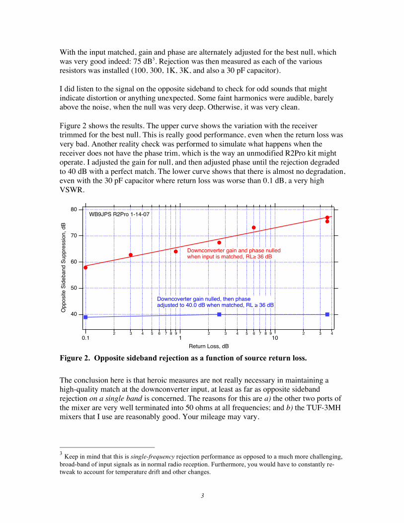
4. Feedback Amplifier Rick Campbell suggested that I try the classic W7ZOI feedback amplifier of Figure 3. It’s very popular in amateur applications for several reasons including overall performance, simplicity, and the ease with which it can be configured for desired gain and DC bias. To obtain high IIP3, high DC collector current must be established, around 50 mA. The 2N5109 is a good choice here because it typically has a low NF, 1.2 GHz ft, is easy to heatsink, and costs about $1.80 from Mouser. I used a small clip-on sink and it only gets warm to the touch. The schematic shows a version that as a gain of 13 dB. I added a small capacitor in the emitter circuit Ctrim, to flatten the high-frequency response a bit. You should experiment with this value. To choose resistor values, I created a spreadsheet with formulas from EMRFD, page 2.25. That gets you very close.
Figure 3. Transformer-coupled feedback amplifier after W7ZOI.
Gain is 13 dB. Frequency response was pleasingly flat, down 0.5 dB at 50 MHz. IIP3 was +27.6 dBm. The easiest way to improve intercept is to increase the power supply voltage. Increasing bias current doesn’t help much above 50 mA, but it does degrade noise figure.
5
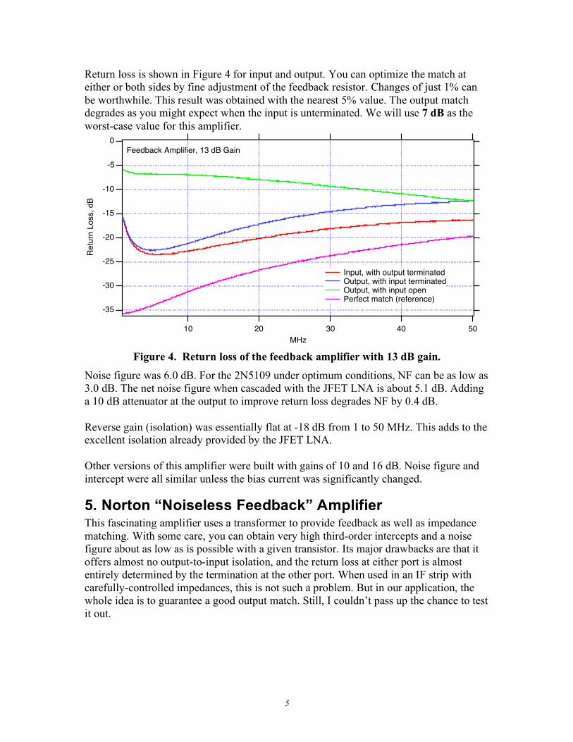
Return loss is shown in Figure 4 for input and output. You can optimize the match at either or both sides by fine adjustment of the feedback resistor. Changes of just 1% can be worthwhile. This result was obtained with the nearest 5% value. The output match degrades as you might expect when the input is unterminated. We will use 7 dB as the worst-case value for this amplifier.
-35
-30
-25
-20
-15
-10
-5
0
Re
turn
Lo
ss,
dB
5040302010
MHz
Feedback Amplifier, 13 dB Gain
Input, with output terminated Output, with input terminated Output, with input open Perfect match (reference)
Figure 4. Return loss of the feedback amplifier with 13 dB gain.
Noise figure was 6.0 dB. For the 2N5109 under optimum conditions, NF can be as low as 3.0 dB. The net noise figure when cascaded with the JFET LNA is about 5.1 dB. Adding a 10 dB attenuator at the output to improve return loss degrades NF by 0.4 dB. Reverse gain (isolation) was essentially flat at -18 dB from 1 to 50 MHz. This adds to the excellent isolation already provided by the JFET LNA. Other versions of this amplifier were built with gains of 10 and 16 dB. Noise figure and intercept were all similar unless the bias current was significantly changed.
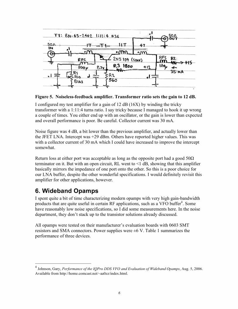
5. Norton “Noiseless Feedback” Amplifier This fascinating amplifier uses a transformer to provide feedback as well as impedance matching. With some care, you can obtain very high third-order intercepts and a noise figure about as low as is possible with a given transistor. Its major drawbacks are that it offers almost no output-to-input isolation, and the return loss at either port is almost entirely determined by the termination at the other port. When used in an IF strip with carefully-controlled impedances, this is not such a problem. But in our application, the whole idea is to guarantee a good output match. Still, I couldn’t pass up the chance to test it out.
6
Figure 5. Noiseless-feedback amplifier. Transformer ratio sets the gain to 12 dB. I configured my test amplifier for a gain of 12 dB (16X) by winding the tricky transformer with a 1:11:4 turns ratio. I say tricky because I managed to hook it up wrong a couple of times. You either end up with an oscillator, or the gain is lower than expected and overall performance is poor. Be careful. Collector current was 30 mA. Noise figure was 4 dB, a bit lower than the previous amplifier, and actually lower than the JFET LNA. Intercept was +29 dBm. Others have reported higher values. This was with a collector current of 30 mA which I could have increased to improve the intercept somewhat. Return loss at either port was acceptable as long as the opposite port had a good 50Ω terminator on it. But with an open circuit, RL went to <1 dB, showing that this amplifier basically mirrors the impedance of one port onto the other. So this is a poor choice for our LNA buffer, despite the other wonderful specifications. I would definitely revisit this amplifier for other applications, however.
6. Wideband Opamps I spent quite a bit of time characterizing modern opamps with very high gain-bandwidth products that are quite useful in certain RF applications, such as a VFO buffer4. Some have reasonably low noise specifications, so I did some measurements here. In the noise department, they don’t stack up to the transistor solutions already discussed. All opamps were tested on their manufacturer’s evaluation boards with 0603 SMT resistors and SMA connectors. Power supplies were ±6 V. Table 1 summarizes the performance of three devices.
4 Johnson, Gary, Performance of the IQPro DDS VFO and Evaluation of Wideband Opamps, Aug. 5, 2006. Available from http://home.comcast.net/~aa0zz/index.html.
7
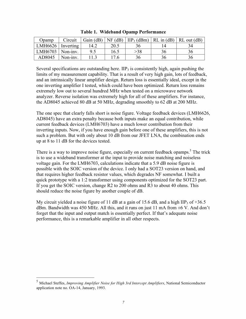
Table 1. Wideband Opamp Performance
Opamp Circuit Gain (dB) NF (dB) IIP3 (dBm) RL in (dB) RL out (dB) LMH6626 Inverting 14.2 20.5 36 14 34 LMH6703 Non-inv. 9.5 16.5 >38 36 36 AD8045 Non-inv. 11.3 17.6 36 36 36
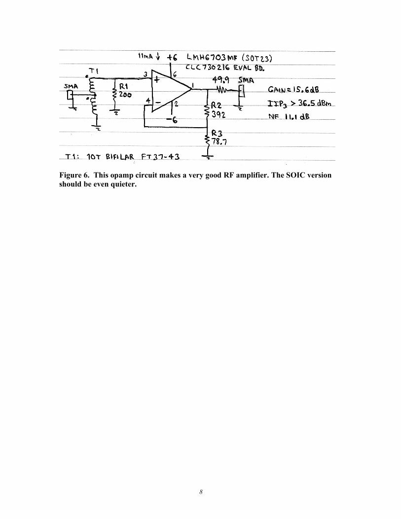
Several specifications are outstanding here. IIP3 is consistently high, again pushing the limits of my measurement capability. That is a result of very high gain, lots of feedback, and an intrinsically linear amplifier design. Return loss is essentially ideal, except in the one inverting amplifier I tested, which could have been optimized. Return loss remains extremely low out to several hundred MHz when tested on a microwave network analyzer. Reverse isolation was extremely high for all of these amplifiers. For instance, the AD8045 achieved 80 dB at 50 MHz, degrading smoothly to 62 dB at 200 MHz. The one spec that clearly falls short is noise figure. Voltage feedback devices (LMH6626, AD8045) have an extra penalty because both inputs make an equal contribution, while current feedback devices (LMH6703) have a much lower contribution from their inverting inputs. Now, if you have enough gain before one of these amplifiers, this is not such a problem. But with only about 10 dB from our JFET LNA, the combination ends up at 8 to 11 dB for the devices tested. There is a way to improve noise figure, especially on current feedback opamps.5 The trick is to use a wideband transformer at the input to provide noise matching and noiseless voltage gain. For the LMH6703, calculations indicate that a 5.9 dB noise figure is possible with the SOIC version of the device. I only had a SOT23 version on hand, and that requires higher feedback resistor values, which degrades NF somewhat. I built a quick prototype with a 1:2 transformer using components optimized for the SOT23 part. If you get the SOIC version, change R2 to 200 ohms and R3 to about 40 ohms. This should reduce the noise figure by another couple of dB. My circuit yielded a noise figure of 11 dB at a gain of 15.6 dB, and a high IIP3 of +36.5 dBm. Bandwidth was 450 MHz. All this, and it runs on just 11 mA from ±6 V. And don’t forget that the input and output match is essentially perfect. If that’s adequate noise performance, this is a remarkable amplifier in all other respects.
5 Michael Steffes, Improving Amplifier Noise for High 3rd Intercept Amplifiers, National Semiconductor application note no. OA-14, January, 1993.
8
Figure 6. This opamp circuit makes a very good RF amplifier. The SOIC version should be even quieter.
9
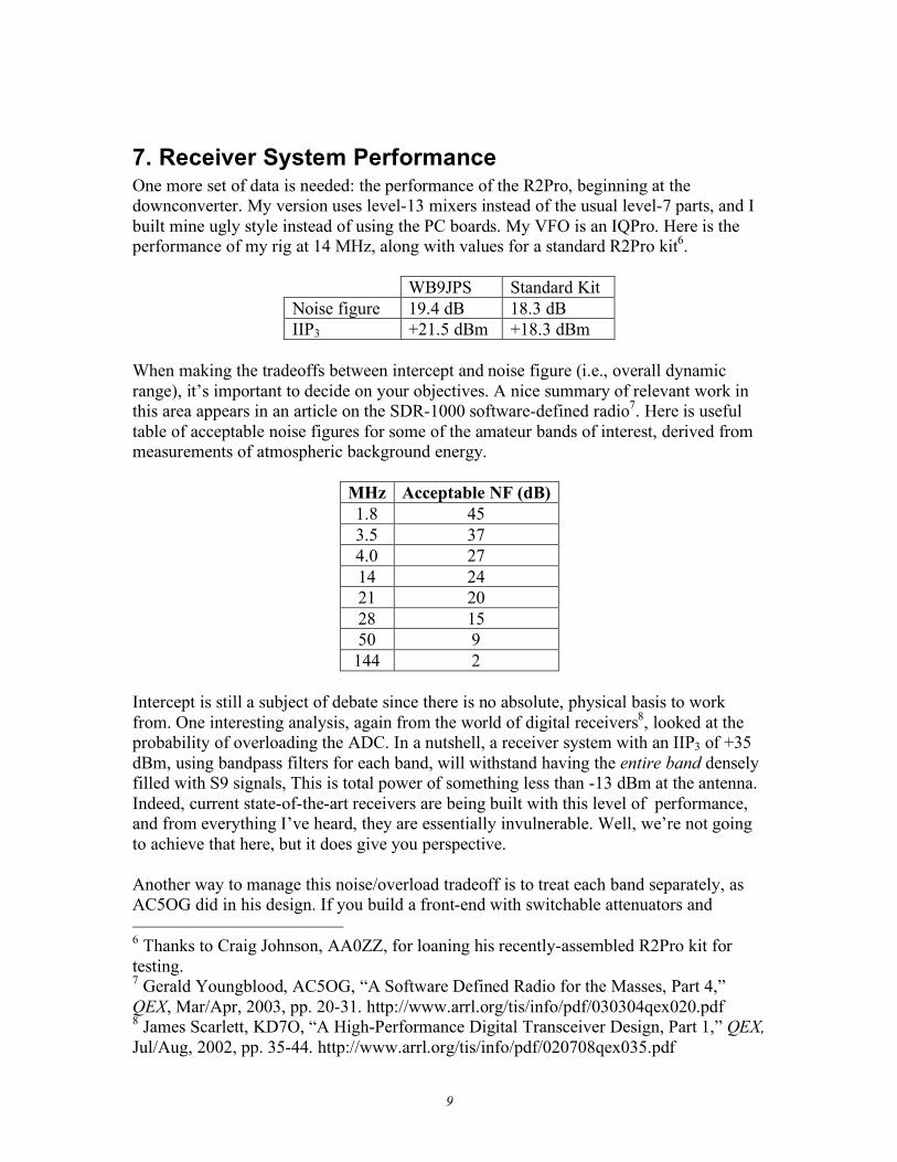
7. Receiver System Performance One more set of data is needed: the performance of the R2Pro, beginning at the downconverter. My version uses level-13 mixers instead of the usual level-7 parts, and I built mine ugly style instead of using the PC boards. My VFO is an IQPro. Here is the performance of my rig at 14 MHz, along with values for a standard R2Pro kit6.
WB9JPS Standard Kit Noise figure 19.4 dB 18.3 dB IIP3 +21.5 dBm +18.3 dBm
When making the tradeoffs between intercept and noise figure (i.e., overall dynamic range), it’s important to decide on your objectives. A nice summary of relevant work in this area appears in an article on the SDR-1000 software-defined radio7. Here is useful table of acceptable noise figures for some of the amateur bands of interest, derived from measurements of atmospheric background energy.
MHz Acceptable NF (dB) 1.8 45 3.5 37 4.0 27 14 24 21 20 28 15 50 9
144 2 Intercept is still a subject of debate since there is no absolute, physical basis to work from. One interesting analysis, again from the world of digital receivers8, looked at the probability of overloading the ADC. In a nutshell, a receiver system with an IIP3 of +35 dBm, using bandpass filters for each band, will withstand having the entire band densely filled with S9 signals, This is total power of something less than -13 dBm at the antenna. Indeed, current state-of-the-art receivers are being built with this level of performance, and from everything I’ve heard, they are essentially invulnerable. Well, we’re not going to achieve that here, but it does give you perspective. Another way to manage this noise/overload tradeoff is to treat each band separately, as AC5OG did in his design. If you build a front-end with switchable attenuators and 6 Thanks to Craig Johnson, AA0ZZ, for loaning his recently-assembled R2Pro kit for testing. 7 Gerald Youngblood, AC5OG, “A Software Defined Radio for the Masses, Part 4,” QEX, Mar/Apr, 2003, pp. 20-31. http://www.arrl.org/tis/info/pdf/030304qex020.pdf 8 James Scarlett, KD7O, “A High-Performance Digital Transceiver Design, Part 1,” QEX, Jul/Aug, 2002, pp. 35-44. http://www.arrl.org/tis/info/pdf/020708qex035.pdf
10
amplifiers, you can dynamically optimize based on the band or even the conditions of the moment. For instance, 40 m is famous for high-power international AM transmitters and heavy contest action, but at the same time, the noise figure requirement is not so stringent. There, we would lean towards a somewhat noisier receiver but with a higher intercept.
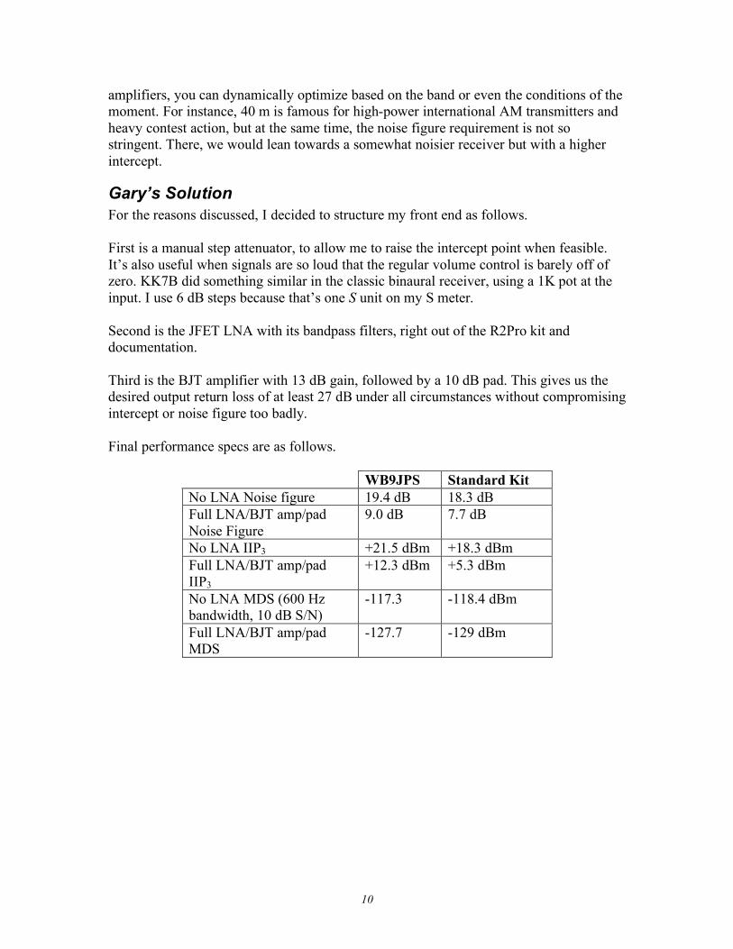
Gary’s Solution For the reasons discussed, I decided to structure my front end as follows. First is a manual step attenuator, to allow me to raise the intercept point when feasible. It’s also useful when signals are so loud that the regular volume control is barely off of zero. KK7B did something similar in the classic binaural receiver, using a 1K pot at the input. I use 6 dB steps because that’s one S unit on my S meter. Second is the JFET LNA with its bandpass filters, right out of the R2Pro kit and documentation. Third is the BJT amplifier with 13 dB gain, followed by a 10 dB pad. This gives us the desired output return loss of at least 27 dB under all circumstances without compromising intercept or noise figure too badly. Final performance specs are as follows.
WB9JPS Standard Kit No LNA Noise figure 19.4 dB 18.3 dB Full LNA/BJT amp/pad Noise Figure
9.0 dB 7.7 dB
No LNA IIP3 +21.5 dBm +18.3 dBm Full LNA/BJT amp/pad IIP3
+12.3 dBm +5.3 dBm
No LNA MDS (600 Hz bandwidth, 10 dB S/N)
-117.3 -118.4 dBm
Full LNA/BJT amp/pad MDS
-127.7 -129 dBm
11
Appendix A Intercept and Noise Figure Measurement and Calculations
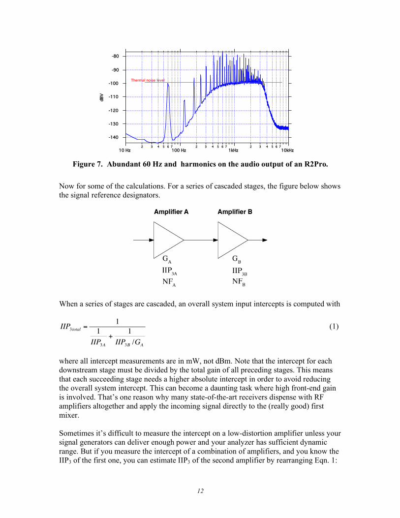
Measurement techniques and formulas for IMD intercept and noise figure that I use come from EMRFD, chapters 2, 6 and 7. For IMD measurements, I use a pair of crystal oscillators running at about 14 MHz and separated by 15 kHz. When characterizing components (like amplifiers), I measured the distortion on a spectrum analyzer. When characterizing a receiver, I use the standard technique where you measure the output voltage at the speaker at one of the intermodulation frequencies (e.g., 2f2 - f1), then tune over to one of the carriers and apply attenuation until the voltage equals that of the IMD signal. For noise figure measurements, I use a calibrated noise source9. To test an amplifier, I measure the hot and cold (on and off) output noise powers with a spectrum analyzer. Since the analyzer is pretty noisy itself, I use one or two Mini-Circuits MAR-6 amplifiers as a preamp. You do have to watch out for overload when cascading these, however, especially if the amplifier under test has no bandpass filter or if it has high gain. To test a receiver, I pass the speaker output through an audio bandpass filter and then to a true RMS voltmeter. The filter I use is an old Rockland (Wavetek) with well-calibrated 8th order high- and low-pass filter sections. That way, the bandwidth is always known. This setup can also measure minimum detectable signal (MDS) when used with a calibrated weak-signal oscillator. A problem was found when testing the R2Pro, one that could easily affect other receivers. There is residual 60 Hz hum and especially its harmonics present on the audio output(Figure 7). If you use the filter-and-voltmeter method, that hum/buzz energy adds to the noise. I was disturbed for the longest time when all my receiver noise figure measurements were about 10 dB higher than expected. It was all hum! Clearly, more effort is required to get rid of the hum. But in the meantime, I switched to an audio spectrum analyzer10 as the measuring device. Then, you can pick out the thermal noise floor between the hum harmonics, and use that level instead. Results reported here are based on that technique.
9 W. Sabin, “A Calibrated Noise Source for Amateur Radio,” QST, May, 1994, p. 37-40. Procedure also covered in EMRFD p. 2.20 and in ARRL Handbook. 10 I used the built-in audio input on my computer and a program I wrote in LabVIEW. Also, there are many freeware and shareware spectrum analyzer applications. This is an extremely useful tool.
12
-140
-130
-120
-110
-100
-90
-80
dBV
10 Hz2 3 4 5 6 7
100 Hz2 3 4 5 6 7
1kHz2 3 4 5 6 7
10kHz
Thermal noise level
Figure 7. Abundant 60 Hz and harmonics on the audio output of an R2Pro.
Now for some of the calculations. For a series of cascaded stages, the figure below shows the signal reference designators.
When a series of stages are cascaded, an overall system input intercepts is computed with
!
IIP3total
=1
1
IIP3A
+1
IIP3B/G
A
(1)
where all intercept measurements are in mW, not dBm. Note that the intercept for each downstream stage must be divided by the total gain of all preceding stages. This means that each succeeding stage needs a higher absolute intercept in order to avoid reducing the overall system intercept. This can become a daunting task where high front-end gain is involved. That’s one reason why many state-of-the-art receivers dispense with RF amplifiers altogether and apply the incoming signal directly to the (really good) first mixer. Sometimes it’s difficult to measure the intercept on a low-distortion amplifier unless your signal generators can deliver enough power and your analyzer has sufficient dynamic range. But if you measure the intercept of a combination of amplifiers, and you know the IIP3 of the first one, you can estimate IIP3 of the second amplifier by rearranging Eqn. 1:
13
!
IIP3B
=G
A
1
IIP3total
"1
IIP3A
(2)
Example: Stage A is the JFET LNA with GA = 10.5 dB (11.2X) and IIP3A = +19 dBm (79.4 mW). Cascading a second amplifier, stage B, produces IIP3total = +13.5 dBm (22.4 mW). Plugging those values into Eqn. 2, we find that stage B has an intercept of +25.4 dBm. Don’t be surprised if the result from this formula doesn’t agree with the result you get when directly measuring intercept of the second stage amplifier by itself. Distortion is by its nature a nonlinear process and simple formulas typically can’t describe the whole situation with high accuracy. Also, distortion products from one amplifier may be in or out of phase with those of the other, so it’s not just simple addition. Even a good numerical simulation, such as SPICE, can only provide an estimate. But these computation are a starting point. Noise figures in a cascaded system are computed with
!
Ftotal
= FA
+FB"1
GA
(3)
Where Fi is the noise factor for a given stage, which is related to noise figure (NF, in dB) by
!
F =10NF /10 and
!
NF(dB) =10LogF (4) Example: Stage A has a gain of 16 dB (Ga=40) and a NF of 5.6 dB (FA=3.63). Adding an output attenuator of 10 dB (Fb=10) degrades the net noise figure to
!
Ftotal
= 3.63 +10 "1
40= 3.86, or 5.86 dB
The fact that the noise of a second stage is divided by the gain of the first stage means that noise figure in later stages is relatively less important. This is where additional RF gain works in your favor. Just don’t forget that it will overload sooner, and your overall dynamic range will suffer to some degree.
14
Acknowledgements I wish to thank Wes Hayward, W7ZOI, and especially Rick Campbell, KK7B, for their valuable reviews and advice on this project, as well as their long-term contributions to the amateur radio community. Thanks also to Craig Johnson, AA0ZZ, for loaning me his R2Pro and for pushing forward with a multiband front-end kit based on this work. About the Author Gary W. Johnson, WB9JPS, is an instrumentation engineer at the Lawrence Livermore National Laboratory. He has a BS degree in electrical engineering/bioengineering from the University of Illinois. His professional interests include measurement and control systems, electro-optics, communications, transducers, circuit design, and technical writing. He is the author of two books and holds nine patents. In his spare time, he enjoys woodworking, bicycling, and audio. He and his wife, Katharine, a scientific illustrator, live in Livermore, California, with their Afghan hound, Chloe. His email is [email protected].


![Multiband Transceivers - [Chapter 1]](https://img.pdfslide.net/doc/110x75/55cf041ebb61ebb0078b482c/multiband-transceivers-chapter-1.jpg)