Embed Size (px)
Citation preview

The 31st International Electric Propulsion Conference, University of Michigan, USA
September 20 – 24, 2009
1
Measuring sputter yields of ceramic materials
IEPC-2009-240
Presented at the 31st International Electric Propulsion Conference,
University of Michigan • Ann Arbor, Michigan • USA
September 20 – 24, 2009
Michael Tartz*, Thomas Heyn
†, Carsten Bundesmann
‡ and Horst Neumann
§
Leibniz-Institute of Surface Modification, Leipzig, 04318, Germany
This paper describes the sputter yield measurements on isolating materials. To avoid
charging of the non-conducting target a neutralizer is employed. The target current is
determined from reference measurements of a material with known sputter yield. Strong
effects of the neutralizing electrons on the ion beam properties at the target were found.
Therefore, a comprehensive characterization of the ion properties at the target has been
performed. The sputter yield of quartz, alumina (Al2O3) and boron nitride (BN) under
normal xenon ion incidence has been measured in the energy range 100 to 800 eV.
I. Introduction
When an energetic particle hits a material surface, it transfers energy and momentum to the material atoms;
some of them can gain enough energy to leave the material. This process is called sputtering and is
quantitatively described by the sputter yield as the average number of ejected particles per incident (energetic)
particle. In electric propulsion, the detailed knowledge of the sputter yield is of high importance for lifetime
estimations of the ion propulsion devices and all satellite components, which might be subject of ion
impingement by the ion beam plume or ions from secondary processes. Also for terrestrial applications of
plasmas and ion beams for various surface modification technologies the sputter yield is an important material
and process parameter.
In gridded ion thrusters the lifetime is mainly limited by the erosion of the ion extraction grids due to
impingement of charge-exchange ions1. In a Hall thruster, the acceleration channel walls are suffering from
strong erosion by ions from the discharge plasma2. Other satellite components as solar arrays or optical elements
can also be hit by primary beam or secondary ions, which might lead to a degradation of the component and
affects its performance and, eventually, its lifetime.
Although there exists a large database of sputter yields, for many relevant material-target combinations one
is faced with a lack of data. Particularly for compound materials like ceramics the supply of sputter data from
literature is poor.
At IOM, sputter yield measurements of ion thruster grid materials like graphites3 and various metals
4 have
been performed. The pertinent sputter yields were found in a good agreement with results from other groups if
available.
Recently, the interest has grown in the sputter behavior of isolating materials, which, however, is a much
more complicated experimental task. The impingement of positively charged ions on the isolating surface leads
to a charging of the surface, which affects the energy of the following arriving ions and has an influence on the
ion beam transport to the target. In order to avoid the surface charging, the ion beam current has to be
neutralized by adding a suitable amount of electrons to the beam. This implicates that it is no longer possible to
measure the target current directly, which however is a required parameter.
The IOM sputter facility and procedures were adapted in order to measure sputter yields of an isolating
material with a current-neutralized beam. A hot-cathode neutralizer was added to the ion source. The unknown
target current is determined from a reference measurement of a material with a well-known sputter yield.
* Senior scientist, Department of Ion Beam Technology, [email protected]
† Master Student, University of Leipzig
‡ Senior scientist, Department of Ion Beam Technology, [email protected]
§ Senior scientist, Department of Ion Beam Technology, [email protected]

The 31st International Electric Propulsion Conference, University of Michigan, USA
September 20 – 24, 2009
2
QMS
load
lock
main
chamber
ion source
Figure 1: The IOM sputter test facility with load-lock,
dc ion source and quadrupole mass spectrometer for
residual gas analysis.
At first, it was investigated how the neutralization influences the properties of the ion beam, which are
essential for the sputter yield determination. The aim was to define the operation conditions and procedures in
order to ensure long-time stable conditions and to define the target current. Initial sputter yield results are
presented for quartz, alumina (Al2O3) and Boron Nitride (BN) under normal xenon ion incidence for energies
between 100 and 800 eV.
II. Experimental setup
A. The sputter test facility
The sputter behavior is investigated in a dedicated
UHV chamber at IOM (Figure 1), which is evacuated
by a turbo pump (2000 l/s) to a background pressure of
less than 10-8
mbar. As a result of the xenon gas flow
through the ion beam source the process pressure
increases up to 5*10-5
mbar. The residual gas
composition is permanently controlled by a quadrupole
mass spectrometer yielding very low contents of water
(many orders of magnitude lower than xenon), pure
oxygen was not detected. This ensures that additional
chemical etching on the sputter samples in presence of
oxygen practically does not occur.
The samples are transferred into the vacuum
chamber by a load-lock chamber and a pushing rod in
order to keep the extraordinary vacuum in the
measurement chamber.
The xenon ion beam is produced by an ISQ 40 DC
Kaufman type ion source (Figure 2) as developed at
IOM. The advantage of the Kaufman type ion source is
the very well-defined ion energy and the very low
energy spread compared to the previously used rf ion
source (see section III.A). The initial beam diameter is
3 cm. A low divergence three-grid extraction system is
used to apply a high ion current density up to 3
mA/cm2 on the target. The source operates at ion
energies up to 1200 eV, on the low-energy side
practically down to a few electron volts. The source
can be operated with almost all non-reactive gases, for
the measurements presented here xenon gas is feed by a mass flow controller.
The sputter targets are placed in the beam centre at a distance of 13 cm from the grids. The targets can be
tilted relative to the beam direction. For non-isolating targets the target current is directly measured and logged
by a computer.
The measured target current has to be corrected by the amount of charge-exchange ions created between ion
source and target, which contribute to the sputtering process but not to the current measurement 5 by a factor
σnde
−, with n being the neutral density, d the distance to the target and σ the charge-exchange cross section.
The resulting correction factor was around 0.95.
Another correction to the target current had to be done for the occurrence of secondary electron emission
during ion bombardment, which virtually increases the measured target current. The supply of experimental
emission coefficients is poor particularly in the low energy region (i.e. < 1000 eV) under investigation here. The
existing values suggest that the secondary electron emission is very low, therefore it was neglected.
The samples are weighed before and after sputtering employing a high-precision microbalance with a
precision of 10 µg. The sputter time had to be chosen large enough to obtain a reliable detectable mass
difference (usually at least 1 mg). The sputter yield is estimated from the weight loss, the sputter time and the
corrected target current.
The samples were prepared from the respective material (purity of at least 99.9%) as it was delivered. Before
first measurement all samples were presputtered in order to avoid the influence of the surface roughness or the
primary ion implantation and sticking on the sputter result. Most of the samples were sputtered consecutively
many times.
The 31st International Electric Propulsion Conference, University of Michigan, USA
September 20 – 24, 2009
3
Figure 2: Kaufman type ion beam source ISQ40DC.
B. Modifications of the setup for isolating materials
The investigation of isolating materials requires the addition of electrons to the ion beam in order to avoid
the charging of the target. A directly heated tungsten hot-filament neutralizer cathode is placed close to the ion
beam. If the neutralizer filament is placed within the ion beam a very efficient coupling of the electrons to the
beam is achieved. On the other hand, the lifetime of the filament is significantly reduced if it is directly hit by
the ion beam. Because of the lifetime issue, in this study the filament was placed outside but closely enough to
the ion beam enabling a coupling to the beam. This results in somewhat larger electron currents to obtain the
same effect on the target as with an in-beam filament. The neutralizer can be set to an additional potential UN.
The emitted electron current is controlled by the applied heating current and the neutralizer potential UN.
The target is now electrically isolated mounted, which enables measuring of the potential of the target Utarget
due to the charging. This value provides a reference for monitoring the experiment.
The sputter yield measurements were performed under conditions where the target is neutralized
(Utarget=0V). The target current is determined from a measurement with a material of well-known sputter yield.
Here, silver was used, which has the advantage of a very high sputter yield and a low sputter threshold and
therefore low sputter time even at low ion energies. Other materials were also tested for use as reference, no
significant effect on the sputtering target current was found (see III.D).
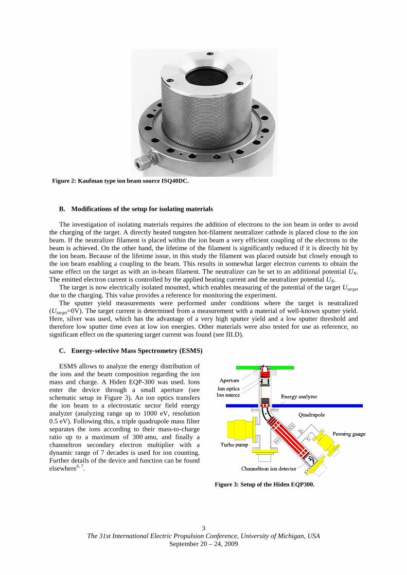
C. Energy-selective Mass Spectrometry (ESMS)
ESMS allows to analyze the energy distribution of
the ions and the beam composition regarding the ion
mass and charge. A Hiden EQP-300 was used. Ions
enter the device through a small aperture (see
schematic setup in Figure 3). An ion optics transfers
the ion beam to a electrostatic sector field energy
analyzer (analyzing range up to 1000 eV, resolution
0.5 eV). Following this, a triple quadrupole mass filter
separates the ions according to their mass-to-charge
ratio up to a maximum of 300 amu, and finally a
channeltron secondary electron multiplier with a
dynamic range of 7 decades is used for ion counting.
Further details of the device and function can be found
elsewhere6, 7
.
Figure 3: Setup of the Hiden EQP300.

The 31st International Electric Propulsion Conference, University of Michigan, USA
September 20 – 24, 2009
4
III. Ion beam properties and neutralization effects
Precise knowledge of the amount and the properties of the sputtering particles is necessary for performing
sputter measurements. While with conductive targets the determination of the ion energy and current is quite
straightforward, the situation is more difficult in the case of an isolation target because of the added neutralizing
electrons. Therefore, a comprehensive characterization of the ion beam has been performed in order to ensure
the beam properties and verify the measurement principle.
A. The ion energy distribution
At first, the ion energy distribution of the used ion source ISQ40DC was investigated by ESMS. Figure 4
shows the energy spectra of 131
Xe isotope ions at various beam voltages. It can be seen, that the ion energy
distribution is rather small (FWHM about 11 eV and below, increasing with ion energy) with a tail to lower
energies of at least two orders of magnitude lower intensity. The main ion energy corresponds to the pre-set
beam voltage also down to very low ion energies, which is characteristic for Kaufman type ion sources.
Therefore, this source was selected for the sputter measurements.
The beam composition has been determined from the mass spectra, proving a very low content of double
charged ions of below 1% thanks to the low discharge voltage of 25 V, which was used throughout this study.
With increasing discharge voltage the content of double charged ions is growing.
B. Ion beam without neutralization
The ion beam was characterized without neutralization in order to define suitable operational parameters for
sputter experiments. The beam current (IBeam), the currents on the accelerator grid (Iacc), on the decelerator grid
(Idec) and the target current (ITarget) were taken in dependence on the accelerator voltage (Uacc) for ion energies of
800 eV and 100 eV.
In Figure 5 (left plot) it can be seen that for increasing accelerator voltage the beam current increases as
expected. The currents on the accelerator and decelerator grids show a minimum. The target current has a
maximum in the region of the minima of the currents on the grids. The behavior of the accelerator and
decelerator currents shows the effect of direct impingement of beam ions on the grids for low accelerator
voltage.
The right plot in Figure 5 shows the situation for a beam voltage of 100 V. The accelerator current for low
accelerator voltage is high and decreases as the accelerator voltage increases. The decelerator current as well
starts with a relatively high value and increases further with the accelerator voltage. The value of the target
0 100 200 300 400 500 600 7000.0
5.0x10⁴
1.0x10⁵
1.5x10⁵
2.0x10⁵
2.5x10⁵
3.0x10⁵
3.5x10⁵
∆ 11 eV
∆ 8 eV
∆ 6 eV
599 eV
299 eV
99 eV
Ubeam
=600 V
Ubeam
=300 V
Ubeam
=100 V
Udischarge
=25V
cou
nts
[a
rb.u
.]
ion energy [eV]
Figure 4: Energy distributions in the ion beam of the ISQ40DC ion source at various beam voltages.

The 31st International Electric Propulsion Conference, University of Michigan, USA
September 20 – 24, 2009
5
current is very low over the shown region (always < 0.1 mA), almost all of the extracted ions arrive on one of
the grids.
The reason for this striking unexpected behavior is believed to be that the compensation of the space charge
induced by the ions is highly insufficient at Ubeam=100 V. It is assumed that the amount of electrons generated
by ionization of beam ions and secondary electron emission at any wall at this low ion energy is not enough to
compensate the space charge.
The IGUN 8-simulations of a beamlet at a beam voltage of 100 V and an accelerator voltage of 1000 V with
and without space charge compensation in Figure 6 illustrate that the ions are deflected at the space charge
outside the source and that most of them hit the decelerator grid as the increased decelerator current in Figure 5
indicates as well. Hence, under these conditions, meaning the weak erosion of target material due to the low
target current and the strong erosion of grid material, no sputter experiments are possible considering the
required time to get a measurable change in target mass and the lifetime of the extraction grids.
This effect of insufficient neutralization can be found up to beam voltages of 300V (see Figure 7).
Conspicuously, there is a sharp transition between the non-compensated and the compensated state. With
increasing beam voltage the transition to the compensated state occurs at a higher value than the transition back
to the non-compensated state with decreasing beam voltage (like a hysteresis). There is currently no satisfying
explanation for this effect, further experiments are necessary.
0 200 400 600 800 1000
16
18
20
22
24
I Bea
m [m
A]
Uacc
[V]
0
1
I acc [m
A]
0.0
0.4
0.8
1.2
I dec [m
A]
6
8
10
I Targ
et [
mA
]U
Beam=800V
0 200 400 600 800 1000
12
15
18
21
24
I Beam [
mA
]
Uacc
[V]
UBeam
=100V
0
3
6
9
12
I acc [m
A]
0
4
8
12
I dec [
mA
]
0.00
0.02
0.04
0.06
0.08
0.10
I Targ
et [
mA
]
Figure 5: Ion beam and grid currents for a beam voltage of 800 V (left) and 100 V (right) at different plasma densities
in dependence on Uacc. Please note that values of Ibeam and Iacc were given by the power supply as integers. Target size
is 2.5x2.5 cm2.
Figure 6: Simulation of beamlet at a beam voltage of 100 V with (top) and without space charge compensation
(bottom).

The 31st International Electric Propulsion Conference, University of Michigan, USA
September 20 – 24, 2009
6
C. Ion beam with neutralization
In order to characterize the influence of the injected electrons on the beam properties the target current (ITarget)
and the current on the decelerator grid (Idec) were taken in dependence on the electron current Ielectron. The target
voltage (UTarget) was measured on the isolated target. The beam currents did not change significantly and are not
shown here. The accelerator voltages were chosen according to Figure 5. An additional voltage UN of -9 V was
applied to the neutralizer.
In Figure 8 the influence of the injected electrons on the ion beam is shown for Ubeam=800 V and 100V. It can be
seen that the target voltage without additional electrons goes up to 530 V (Ubeam=800 V) and 80 V
(Ubeam=100 V) corresponding to 65% and 80% of the beam voltage. The target voltage depends on the space
charge potential, the incoming ion and electron currents and the secondary electron generation on the target.
At Ubeam=800 V, the target current increases up to an electron current of 10 mA with growing electron current,
the maximum is 3% higher than for the case with zero electron current. For a further increasing electron current
150 200 250 300 350 400 450
0.00.20.40.60.81.01.21.41.6
0
2
4
6
8
100
2
4
16
18
I targ
et [
mA
]
Ubeam
[V]
I dec
el [
mA
]
I acc [m
A]
Uacc
=900V
I beam
[m
A]
Figure 7: Ion beam and grid currents in dependence on the beam voltage Ubeam. Uacc=900V
0 50 100 150 200
0.0
0.2
0.4
0.6
0.8
1.0
I de
c [m
A]
Ie- [mA]
4
6
8
10
I Targ
et [
mA
]
0
100
200
300
400
500 Ubeam
=800V
UT
arg
et [
V]
02468
10
I dec [m
A]
0
2
I Targ
et [
mA
]
0
50
100
Ubeam
=100V
UT
arg
et [
V]
0 50 100 150 2000
2
4
Ie- [mA]
I acc [m
A]
Figure 8: Influence of electrons on ion beam and target for a beam voltage of 800 V (left) and 100 V (right).

The 31st International Electric Propulsion Conference, University of Michigan, USA
September 20 – 24, 2009
7
the target voltage and the target current decrease as more electrons reach the target. To obtain a neutralized
target with this setup very high electron currents are needed. The decelerator current is only slightly influenced.
At Ubeam=100V, already a few electrons (<3 mA) have a strong effect on the ion beam. The currents on the
accelerator and the decelerator grid are reduced to reasonable values. The target voltage starts at 80 V and
decreases with increasing electron current. For Ielectron ≈ 5 mA the target current reaches its maximum which is
20 times the value with zero electron current.
The possible explanation for these strong effects is that the emitted electrons significantly enhance the space
charge compensation. The few added electrons are able to initiate further ionization processes at the residual gas
and secondary processes at surfaces, which results in an increased number of electrons for the space charge
compensation. While without additional electrons most of the ions return towards the ion source, now the ion
beam leaves the grids and moves through the chamber. Consequently, the ion beam behaves as it would be
expected as is shown in Figure 9. The inset of direct impingement was found at Uacc= 800 V, corresponding to
Uextraction=900 V, which agrees well to the value for Ubeam=800 V (see Figure 5).
In order to further characterize the ion beam profile on an isolating target, the footprint of the beam on SiO2-
layers of known thickness on silicon wafers was investigated. The thickness of the SiO2-layers after sputtering
was measured optically (see example in Figure 10). For a better comparability of the various conditions the
erosion rate ∆s in nm/min is determined and used.
It was found, that the position of the beam center is independent on the electron current with respect to the
accuracy of the measurement (see Figure 11). The non rotational symmetric filament neutralizer has obviously
no effect on the beam symmetry, no asymmetric beam profiles were found.
The erosion rate at the beam center (∆smax) strongly increases for small amounts of injected electrons (see Figure
12). The growing maximal erosion rate agrees well with the strong increase of the target current and the
reducing target charging (Figure 8, right plot). For further increasing electron current the maximum erosion rate
reduces, also the total erosion of the eroded volume reduces. This can be traced back only to a reduced target
current as it is demonstrated in the next section.
400 500 600 700 800 900 1000
12
15
I Bea
m [m
A]
Uacc
[V]
03
6
912
I acc [m
A]
0
4
8
I dec [m
A]
0.0
0.5
1.0
1.5
2.0
I
e-=0mA
Ie-=3mA; U
n=2V
I Targ
et [
mA
]
Figure 9: Comparison of ion beam properties with and without electron emission at Ubeam=100V.

The 31st International Electric Propulsion Conference, University of Michigan, USA
September 20 – 24, 2009
8
D. Target current
The target current has been directly measured from a molybdenum and aluminum target in dependence on the
neutralizer voltage UN, i.e. the negative potential applied to the neutralizer cathode**
. This potential is usually set
negative in order to increase the amount of electrons emitted by the cathode according to the space-charge
limited conditions. The electron current has been set to 4.5 mA. As shown in Figure 13, the target current drops
when the neutralizer is set to a few volts negative and then increases with UN (i.e. UN gets more negative, see
footnote). When exceeding about 40V, the target current differs for both materials. The secondary electron
emission coefficient (SEEC) for electron impact is larger for molybdenum than for aluminum (clean) (see
Figure 14) [9, 10], the coefficients apparently differ at energies above 50 eV. The larger SEEC of molybdenum
virtually increases the target current more than with aluminum as can be seen in the figure.
**
Please note that UN gives the absolute value of the negative potential.
5
10
15
20
25
30
400
600
800
5
10
15
20
25
30
Layer
thic
kness [nm
]
Y [mm
]X [mm]
UBeam
=100V; Ie-=2mAfixing clip
Figure 10: Measured thickness of SiO2-layer after
sputtering at a beam voltage of 100 V (initial value is 800
nm)
10 12 14 16 18 20
6
8
10
12
14
Y [m
m]
X [mm]
Figure 11: Center of ion beam for different electron
currents (2, 5, 20, 100 and 195 mA)
0 50 100 150 200 250 300 3501
2
3
4
5
Ielectron
[mA]
∆s
max [
nm
/min
]
Figure 12: Erosion rate at beam center (maximum erosion rate) ∆smax for SiO2 sputtered at a beam voltage of
100 V.

The 31st International Electric Propulsion Conference, University of Michigan, USA
September 20 – 24, 2009
9
With the higher electron current of 100 mA the measured target currents are lower (compare to Figure 8),
however, the measured current of the higher-SEEC material molybdenum is lower than that of aluminum. The
reason for this contrary behavior is currently ambiguous.
The directly measured target currents are affected by the rather unknown content of electrons arriving at the
target. The electrons could be suppressed by biasing the target which, however, may produce other effects on
the ion beam.
In order to determine the content of ions (i.e. the
sputtering particles), reference measurements were
performed using a material with a well-known sputter
yield. The effective sputtering current Itarget,sput is
determined from the mass loss, the sputter time and the
known sputter yield. This procedure is also used to
determine the target current before any sputter
measurement of isolating materials.
This approach largely avoids all participation of the
electrons on the target current, but depends on the
assumption that the sputtering particles have a well-
known energy. The ion energy is affected by the target
potential, which can be measured in case of a conducting
target, but which can only be approximated in case of an
isolating target material to be the same as that of the
sample mounting parts. The ion energy distribution has
been investigated (see section III.A) to correspond
accurately to e*Ubeam (grounded target).
It has been found that the sputtering target current
strongly depends on the electron parameters. Figure 15
shows the target current Itarget,sput and target potential in
dependence on the electron current for silver and
tungsten targets (the target potential has been considered in the sputter yield for calculating the target current).
Figure 16 gives the target current in dependence on the neutralizer potential UN for a fixed electron current.
With growing electron current the Itarget,sput shows a maximum which is found at a target voltage of about
18 V. A further growing electron current reduces the sputtering target current. At Ubeam=500 V, for a neutralized
target an electron current of 300 mA is required, the sputtering target current is 20% lower than at the
maximum. At 100 V, similar relations are found. The sputtering target current reduces with growing electron
current.
0 20 40 60 80 100 120 140
0.2
0.3
0.4
0.5
0.6
0.7
0.8
Ie-=100 mA
Ie-=4.5 mA
Al
Mo
Mo
UN [V]
I targ
et [
mA
]
Figure 13: Directly measured target current at Ubeam=100 V and electron currents of 4.5 mA (black curves) and
100 mA (red) for molybdenum (full symbols) and aluminum (open symbols) in dependence on the neutralizer
voltage.
0 20 40 60 80 100 120 140 1600.2
0.4
0.6
0.8
1.0
1.2
1.4
1.6
1.8
Al oxid
Mo
Al clean
SE
EC
electron energy [eV]
Figure 14: Secondary electron emission coefficients in
dependence on electron energy. Data from [9, 10]

The 31st International Electric Propulsion Conference, University of Michigan, USA
September 20 – 24, 2009
10
Increasing neutralizer voltage UN leads to a larger sputtering target current and a lower target charging
(Figure 16).
No significant effect of the material on the effective sputtering target current was found as it was expected.
The slightly lower currents found for tungsten compared to silver (about 2%) are traced back to a slight
underestimation of the used tungsten sputter yield model (Bohdansky formula3) as compared to own
measurements at tungsten.
Furthermore, a slight decrease of the sputter yield of BN at larger UN was found (see Figure 17) which is
traced back to the effect of the secondary electrons on the target charging and the space charge within the ion
beam. For UN up to 30 V no effect on the sputter yield can be seen.
0 50 100 150 200 250 300 350 400
0.9
1.0
1.1
1.2
1.3
1.4
1.5
-10
0
10
20
30
40
50
60
UN = 10 V
UN = 75 V
Ag
W
I Targ
et,sput [
mA
]
Ielectron
[mA]
Ubeam
= 500 V
UN = 75 V
UN = 10 V
UT
arg
et [
V]
0 50 100 150 200 250 300 350 400
0.25
0.30
0.35
0.40
0.45
0.50
0.55
0.60
0.65
0.70
-10
0
10
20
30
40
I targ
et,sput [
mA
]
Ielectron
[mA]
Ubeam
= 100 V
Uta
rget [
V]
Figure 15: Effective sputtering target current ITarget,sput and target potential UTarget in dependence on electron
current. Top: Ubeam=500V. Bottom: Ubeam=100 V. Target potential considered for current determination.

The 31st International Electric Propulsion Conference, University of Michigan, USA
September 20 – 24, 2009
11
E. Conclusions for the sputter measurements
For reliable sputter measurements precise knowledge of the properties of the sputtering ions is necessary.
Therefore, the effects of the neutralizing electrons on the ion beam and the target have been investigated
thoroughly. Strong impacts of the electron conditions on the space charge, the target charging, the ion beam
properties and, consequently, the properties of the sputtering particles were found.
The results of the beam characterization suggest to perform the sputter experiments at large neutralizer
voltages and lower electron currents where the resulting target current is maximum. However, the target is not
neutralized under such condition which falsifies the sputter yields because of the affected ion energy. Therefore,
it was decided to perform the sputter yield measurements at lower neutralizer voltages (typically 25V were
used) and at electron currents where the target potential measured at the reference target is equal or slightly
below zero volt.
These results demonstrate the complex nature of the sputtering target current under neutralized beam
conditions. In consequence, the target current has to be measured before each sputter experiment.
0 20 40 60 80 100 120 140 1600.9
1.0
1.1
1.2
1.3
1.4
1.5
Ubeam
=500eV
W
Ag
I targ
et,sputt [m
A]
UN [V]
Figure 16: Effective sputtering target current in dependence on neutralizer voltage UN. Ubeam=500 V, Ibeam=18 mA,
Ielectron set to have zero target voltage.
0 20 40 60 80 100 120 140 160
0.035
0.040
0.045
0.050
Utarget
= 0 V
Ubeam
= 500 V
spu
tter
yie
ld [
mg
/C]
UN [V]
Figure 17: Sputter yield of BN measured at various neutralizer voltages UN. Electron current set to Utarget=0V.

The 31st International Electric Propulsion Conference, University of Michigan, USA
September 20 – 24, 2009
12
IV. Sputter yields of ceramics
The sputter yields of ceramic materials have been measured under normal xenon incidence at 100, 250, 350,
500 and 800 eV. The results are given in mm3/C corresponding to the removed volume per Coulomb of
incoming particles. For multicomponent materials as ceramics the usual sputter yield unit “atoms/ion” is not
applicable because the single components may be sputtered differently (preferential sputtering). This leads to an
equilibrium surface composition which may differ from the initial composition.
Our results are compared with available literature data if possible.
A. Sputter yields of quartz and Al2O3
Figure 18 shows the sputter yields of quartz and alumina under normal xenon ion incidence. Our quartz data
is somewhat lower than the results of Yalin et. al. 11
. A good agreement with simulated sputter yields of Tondu
et. al. 12
is found. No other experimental data is found for alumina.
100 200 300 400 500 600 700 800 9000.00
0.05
0.10
0.15
Yalin (AIAA-2007-5314) - QCM
Tondu (AIAA-2008-5090) - simulation SiO2
this study
Xe -> Quartz
Y [m
m3 /C
]
energy [eV]
100 200 300 400 500 600 700 800 9000.00
0.01
0.02
0.03
0.04
this study
Xe -> Al2O
3
Y [m
m3 /C
]
energy [eV]
Figure 18: Sputter yields of quartz (top) and alumina (Al2O3) in dependence on xenon ion energy.

The 31st International Electric Propulsion Conference, University of Michigan, USA
September 20 – 24, 2009
13
B. Sputter yield of BN
The sputter yields were measured using an isotropic pressed high-density BN with Calcium Borate binder
(samples provided by Sindlhauser Materials).
As already reported by others13
BN shows significant moisture absorption. As shown in Figure 19 the mass
of the BN sample increases after taking the sample out of the vacuum to normal atmosphere. After about 8 hours
the steady-state is reached. Although this total mass increase is only less than 0.2% of the sample mass, it is in
the order of the mass change by sputtering. In order to ensure reliable mass values all samples were weighed
after at least 8 hours at normal atmosphere (practically done at the next day). The effect of varying humidity at
different days on the mass was found to be within the weighing measuring error.
Figure 20 shows the BN sputter yields in comparison with other published data 13
,14,1 5,16,
- 17. Our yields are the
lowest and are in agreement with the 2007 CSU weight loss data of HBC grade BN by Rubin et. al.13
. Newer
data from the same group by Topper et. al.17
show much higher sputter yields, the reason for this discrepancy is
currently not clear and under investigation. The agreement with simulated data by Tondu et. al.12
is very good.
100 200 300 400 500 600 700 800 9000.00
0.02
0.04
0.06
0.08
Topper 2008 WL
Topper 2008 QCM
Rubin 2007 HBC WL
Rubin 2007 HBR WL
Semenov 1991
Garnier 1999
Abashkin 2007
Tondu 2008 (simulation)
this study
spu
tte
r yi
eld
[m
m3
/C]
energy [eV]
Figure 20: Sputter yield of BN in dependence on xenon ion energy (normal incidence).
0 100 200 300 400 500
-1.5
-1.0
-0.5
0.0
at t=
0 s
am
ple
was
take
n o
ut of th
e v
acu
um
ma
ss c
ha
nge
[m
g]
time [min]
Figure 19: Moisture absorption of BN sample after 4h xenon bombardment (500 eV). Sample was taken out of the
vacuum at t=0.

The 31st International Electric Propulsion Conference, University of Michigan, USA
September 20 – 24, 2009
14
V. Summary and Outlook
Measuring sputter yields of isolating materials is not an simple task. Many circumstances regarding the ion
beam and target neutralization by electrons may affect the sputter result. The determination of the sputtering
target current requires large attention.
The following table summarizes the measured sputter yields in mm3/C.
Quartz Al2O3 BN
100 eV 0.0132 0.00189 0.00265
250 eV 0.0395 0.0076 0.01
350 eV 0.0577 0.013 0.0133
500 eV 0.076 0.0213 0.021
800 eV 0.118 0.0326 0.034
References
1 M. Tartz, E. Hartmann, H. Neumann, Validated simulation of the ion extraction grid lifetime, Rev. Sci. Instrum. 79
(2008) 02B905; M. Tartz, E. Hartmann, H. Neumann, Paper Nr. AIAA-2006-5001, 42nd Joint Propulsion Conference,
Sacramento, CA, 9.-12.7. 2006. 2 S. Y. Cheng, M. Martinez-Sanchez, Modeling of Hall thruster lifetime and erosion mechanisms, IEPC-2007-250, 30th
International Electric Propulsion Conference, Florence, Italy, 17. - 20.9. 2007. 3 M. Tartz, H. Neumann, Sputter Yields of Carbon Materials under Xenon Ion Incidence, Plasma Process. Polym. 4
(2007) S633. 4 M. Tartz, D. Manova, H. Neumann, H. Leiter, J. Esch, Sputter investigation of ion thruster grid materials, Paper Nr.
AIAA-2005-4414, 41. Joint Propulsion Conference, Tucson, AZ, 10.-13.07. (2005)
5 M. Tartz, E. Hartmann, F. Scholze, H. Neumann, F. Bigl, A new approach to ion beam modelling, Surf. Coat. Technol.
97 (1997) 504. 6 F. Scholze, M. Tartz, H. Neumann, H. J. Leiter, R. Kukies, D. Feili, S. Weis, Ion analytical characterisation of the RIT
22 ion thruster, Paper Nr. AIAA-2007-5216, 43. Joint Propulsion Conference, Cincinnatti, OH, 8.-11.7. (2007). 7 M. Zeuner, H. Neumann, F. Scholze, D. Flamm, M. Tartz, F. Bigl, Characterization of a modular broad beam ion
source, Plasma Sources Sci.Technol. 7 (1998) 252-267. 8 R. Becker, W. B. Herrmannsfeldt, “IGUN - A program for the simulation of positive ion extraction including magnetic
fields”, Rev. Sci. Instrum. 63 (1992) 2756-2758; R. Becker, “New features in the simulation of ion extraction with IGUN”,
Proc. 6. Europ. Particle Accelerator Conf. EPAC98, 22.-26. Juni 1998, Stockholm. 9 R. L. Petry, Phys. Rev. 26 (1925) 346. 10 H. Bruining, J. H. de Boer, Physica V (1938) 2. 11 A. Yalin, B. Rubin, S. Domingue, J. Williams, Z. Glueckert, Differential Sputter Yields Of BN, Quartz, and Kapton By
Xe+ Bombardment, Paper AIAA-2007-5314, 43rd Joint Propulsion Conference, Cincinnatti, OH, 9.-11.7.2007. 12 Th. Tondu, V. Viel-Inguimbert, J- F. Roussel, S. D'Escrivan, Hall Effect Thrusters ceramics sputtering yield
determination by Monte Carlo simulations, Paper Nr. AIAA-2008-5090, 44th Joint Propulsion Conference, Hartford, CT,
21.-23.7. 2008. 13 B. Rubin, J. L. Topper, A. P. Yalin, Total and Differential Sputter Yields Of Boron Nitride Measured by Quartz
Crystal Microbalance and Weight Loss, IEPC-2007-074, 30th International Electric Propulsion Conference, Florence, Italy,
17. - 20.9. 2007. 14 Semenov A., Shkarban, I., Ion Beam Sputtering of the Surfaces of Ion and Plasma Sources, Rocket and Space
Engineering: Rocket Engines and Power Plants, No.3, 1991, 42. 15 Y. Garnier, V. Viel, J.-F. Roussel, J. Bernard, Low-energy xenon ion sputtering of ceramics investigated for stationary
plasma thrusters, J. Vac. Sci. Tech. A 17 (6) pp. 3246-3254.
16, Abashkin, V., Gorshkov, O., Lovtsov, A., and Shagaida, A., Analysis of Ceramic Erosion Characteristic in Hall-
Effect Thruster with Higher Specific Impulse, IEPC-2007-133, 30th International Electric Propulsion Conference, Florence,
Italy, 17. – 20.9. 2007.
17 J. L. Topper, B. Rubin, C. C. Farnell, A. P. Yalin, Preliminary Results of Low Energy Sputter Yields of Boron Nitride
due to Xenon Ion Bombardment, Paper AIAA-2008-5092, 44th Joint Propulsion Conference, Hartford, CT, 21.-23.7.2008.