Embed Size (px)
Citation preview

SLLS566F − MAY 2003 − REVISED MARCH 2009
1WWW.TI.COM
Eight 1.0- to 1.3-Gigabits Per Second(Gbps) Synchronizable Transceivers
Low Power Consumption <1.3 W at1.25 Gbps
IEEE 802.3z Gigabit Ethernet Compliant Differential VML Transmit Outputs With
No External Components Necessary.PECL Compatible Levels
Programmable High-Speed OutputPreemphasis Levels
Selectable Parallel Interface Modes:− Nibble-Wide Double Data Rate (DDR)
Clocking Interface− Multiplexed Channel DDR Clock
Interface Selectable Clock Tolerance
Compensation Selectable On-Chip 8b/10b IEEE 802.3z
Compliant Encoder and Decoder JEDEC-Compliant 1.8-V LVCMOS
(Extendable to 2.5 V)
3.6-V Tolerant Inputs on Parallel I/O Internal Series Termination on LVCMOS
Outputs to Drive 50- Ω Lines Comprehensive Suite of Built-In
Testability Features (PRBS Generationand Verification, Serial Loopback, andFar-End Loopback)
IEEE 802.3 Clause 22 Management DataInterface (MDIO) Support
IEEE 1149.1 JTAG Support Hot-Plug Protection on Serial I/O No External Filter Components
Required for PLLs Small Footprint 19 ×19-mm,
289-Terminal, 1,0-mm Ball-Pitch BGA Advanced Low-Power 0.18- µm CMOS
Technology Commercial Temperature Rating (0 °C to
70°C)
description
The TLK2208A is the third generation of Gigabit Ethernet transceivers from Texas Instruments combining highport density and ultralow power in a small form-factor footprint. The TLK2208A provides for high-speedfull-duplex point-to-point data transmissions based on the IEEE 802.3z 1000-Mbps Ethernet specification. TheTLK2208A supports data rates from 1.0 Gbps through 1.3 Gbps.
The primary application of this device is to provide building blocks for developing point-to-point baseband datatransmission over controlled impedance media of 50 Ω. The transmission media can be printed circuit boardtraces, copper cables or fiber-optical interface modules. The ultimate rate and distance of data transfer isdependent upon the attenuation characteristics of the media and the noise coupling to the environment.
The TLK2208A performs the data encoding, decoding, serialization, deserialization, clock extraction, and clocktolerance compensation functions for a physical layer interface device. Each channel operates at up to 1.3 Gbpsproviding up to 8.32 Gbps of aggregate data bandwidth over copper or optical-media interfaces.
The TLK2208A supports two selectable reduced-pin-count double-data-rate (DDR) timing interfaces, nibblemode and multiplexed channel mode, to a protocol device.
In the nibble interface mode, the parallel interface accepts nibble-wide unencoded or 8b/10b encoded dataaligned to both the rising and falling edges of the transmit clock.
In the multiplexed channel mode, the parallel interface accepts 8-bit-wide unencoded or 10-bit-wide 8b/10bencoded data with channels A, C, E, and G aligned to the falling edge of the source synchronous transmit clockand channels B, D, F, and H aligned to the rising edge of the transmit clock. The receive path interface is donein the same manner.
Copyright 2003 − 2009, Texas Instruments Incorporated
Please be aware that an important notice concerning availability, standard warranty, and use in critical applications ofTexas Instruments semiconductor products and disclaimers thereto appears at the end of this data sheet.
!"# $"%&! '#('"! ! $#!! $# )# # #* "#'' +,( '"! $!#- '# #!#&, !&"'##- && $##(

2 WWW.TI.COM
description (continued)
The TLK2208A aligns the recovered data clock frequency to the reference clock on each channel by meansof a clock tolerance compensation circuit and internal FIFO that inserts or drops 20-bit IDLE codes as neededin the interpacket gap (IPG). In synchronous mode, the received data for all channels is aligned to a singlereceive data clock that is a buffered version of the reference clock.
The TLK2208A supports a selectable IEEE 802.3z compliant 8b/10b encoder/decoder in all its modes ofoperation.
The TLK2208A automatically locks onto incoming data without the need to pre-lock.
The TLK2208A provides a comprehensive series of built-in tests for self-test purposes including loopback andPRBS generation and verification. An IEEE 1149.1 JTAG port is also supported to aid in board-manufacturingtesting.
The TLK2208A is housed in a small form-factor 19×19-mm, 289-terminal BGA with 1,0-mm ball pitch. The ballout and footprint are compatible with those of the PMC-Sierra PM8352 8-channel transceiver.†
The TLK2208A is characterized to support the commercial temperature range of 0°C to 70°C.
The TLK2208A consumes 1.3 W when operating at nominal conditions.
The TLK2208A is designed to be hot-plug capable. A power-on reset puts the serial side output signal terminalsTX+/TX− in the high-impedance state during power up.
MAC/Packet
Processor
8
TLK2208A
TX+
TX−
RX+RX−
TDA..H[9:0]
TCLKB
RCLK
8
8
8
RDA..H[9:0]
Electricalto Optical
Array
Switch Fabric
8
TLK2208A
TX+
TX−
RX+RX−
TDA..H[9:0]
TCLKB
RCLK
8
8
8
RDA..H[9:0]
SystemBackplane
Line Card
8
8
TLK2208A
RDA..H[9:0]
RCLK
TCLKB
TDA..H[9:0]
8
8
8
8
RX+RX−
TX+
TX−
Figure 1. TLK2208A System Implementation Diagram† Functionally compatible with the PM8352 in multiplex channel mode.

3WWW.TI.COM
FIFOTDxx[9:0]
TCLKx
8b/10bEncoder
Serializer TX+/TX−
Transmit Channels A − H
ClockRecovery
RDxx[9:0]
RCLK
8b/10bDecoder RX+/RX−
Receive Channels A − H
FIFO/CTCDeserializer
andByte Align
RBCx
ClockSynthesizerREFCLK
CommonControl Logic
Static Controls
MDIO/MDC
Figure 2. TLK2208A Block Diagram

4 WWW.TI.COM
Pin Out(Top View)
A B C D E F G H J K L M N P R T U
17 GNDA GNDA GNDA GNDA GNDA GNDA GNDA GNDA GNDA GNDA GNDA GNDA GNDA GNDA GNDA GNDA GNDA 17
16 TXH+ TXG+ TXF+ TXE+ TXD+ TXC+ TXB+ TXA+ GNDA RXH+ RXG+ RXF+ RXE+ RXD+ RXC+ RXB+ RXA+ 16
15 TXH− TXG− TXF− TXE− TXD− TXC− TXB− TXA− NC RXH− RXG− RXF− RXE− RXD− RXC− RXB− RXA− 15
14 GNDA GNDA GNDA GNDA GNDA GNDA GNDA GNDA NC GNDA GNDA GNDA GNDA GNDA GNDA GNDA GNDA 14
13 TDHG8 TDHG9PRBS
ENEN
ABLEVDDA VDDA VDDA VDDA VDDA VDDA VDDA VDDA VDDA DVAD2 DVAD1 RDHG9 RDHG8 13
12 TDHG6 TDHG7REFCLK
DVAD4 VDD T-GND VDD MODE1 DVAD0 RDHG7 RDHG6 12
11 TDHG4 TDHG5 TMS DVAD3 VDD VDD MODE0PLL_LOCK
RDHG5 RDHG4 11
10 TDHG2 TDHG3 TCK NC VDD VDD RSVDRCLKRBCH
RDHG3 RDHG2 10
9 TDHG0 TDHG1 TDITCLK_
SELVDDQ VDDQ
BUSYEN
RBCG RDHG1 RDHG0 9
8 TDFE8 TDFE9GE_MOD
TRST VDDQ VDDQ RSVD RBCF RDFE9 RDFE8 8
7 TDFE6 TDFE7 TDO LPBK VDDQ VDDQ RSVD RBCE RDFE7 RDFE6 7
6 TDFE4 TDFE5 TCLKH NC VDDQ VDDQ NC RBCD RDFE5 RDFE4 6
5 TDFE2 TDFE3 TCLKF NC VDDQ VDDQ VDDQ VDDQ VDDQ VDDQ VDDQ VDDQ VDDQ NC RBCC RDFE3 RDFE2 5
4 TDFE0 TDFE1 TCLKD NC GND GND GND GND GND GND GND GND GND RBCA RBCB RDFE1 RDFE0 4
3 TDDC8 TDDC9 TDDC6 TDDC7 TCLKB RSVD RESET MDCCV_
DIS_ENNC NC NC NC RDDC7 RDDC6 RDDC9 RDDC8 3
2 TDDC4 TDDC5 TDDC1 TDBA1 TDBA3 TDBA5 TDBA7 TDBA9 CODE RDBA1 RDBA3 RDBA5 RDBA7 RDBA9 RDDC1 RDDC5 RDDC4 2
1 TDDC3 TDDC2 TDDC0 TDBA0 TDBA2 TDBA4 TDBA6 TDBA8 MDIO RDBA0 RDBA2 RDBA4 RDBA6 RDBA8 RDDC0 RDDC2 RDDC3 1
A B C D E F G H J K L M N P R T U
T-GND T-GND T-GND T-GND T-GND T-GND
T-GND T-GND T-GND T-GND T-GND T-GND T-GND
T-GND T-GND T-GND T-GND T-GND T-GND T-GND
T-GND T-GND T-GND T-GND T-GND T-GND T-GND
T-GND T-GND T-GND T-GND T-GND T-GND T-GND
T-GND T-GND T-GND T-GND T-GND T-GND T-GND
T-GND T-GND T-GND T-GND T-GND T-GND T-GND
NOTE: Unused inputs that do not hold an integrated pullup or pulldown circuit need to be terminated to either VDDQ or GND, respectively, toavoid excessive currents and lifetime degradation.
Figure 3. Terminal Diagram

5WWW.TI.COM
Signal Terminal Description
Serial I/O Signals
SIGNAL LOCATION TYPE DESCRIPTION
TX[A:H]+TX[A:H]–
H16:A16H15:A15
VMLoutput
Differential output transmit. TX[A:H]+ and TX[A:H]– are differential serial outputs that interface to acopper or an optical I/F module.
TX[A:H]+ and TX[A:H]– are put in a high-impedance state when LPBK = high or when the LOOPBACKbit for a particular channel in the MDIO registers is set.
RX[A:H]+RX[A:H]–
U16:K16U15:K15
PECL-compatible
input
Differential input receive. RX[A:H]+ and RX[A:H]– together are the differential serial input interfacefrom a copper or an optical I/F module. Differential resistive termination is built-in for these terminals.
Transmit Data Bus and Clock Signals
SIGNAL LOCATION TYPE DESCRIPTION
REFCLK C12 LVCMOSinput
Reference clock. REFCLK is an external input clock that provides the clock reference forsynchronizing the receiver and transmitter interfaces.
REFCLK is supposed to run from 100 MHz up to 130 MHz for 1 Gbps up to 1.3 Gbps operation of theserial interface.
TCLKB E3 LVCMOSinput with
P/U
Transmit data clock. When in synchronized channel modes, the data on TDBA[9:0], TDDC[9:0],TDFE[9:0] and TDHG[9:0] is latched on both the rising and falling edges of TCLKB.
When in independent channel modes, TCLKB latches TDBA[9:0] data on both its rising and fallingedges.
TCKD,TCKF,TCKH
C4,C5,C6
LVCMOSinput with
P/U
Transmit data clock channels C and D, E and F, G and H. When in independent channel mode, theseterminals are used to latch data for their perspective channels on both the rising and falling edges.TCKD applies to channels C and D, TCKF applies to channels E and F, and TCKH applies to channelsG and H.
TDBA[7:0] G2, G1, F2,F1, E2, E1,
D2, D1
LVCMOSinput
Transmit data channels A and B. The parallel data is clocked into the transceiver on the rising andfalling edges of TCLKB and transmitted as a serial stream with TDBA0 sent as the first bit.
In multiplexed channel mode, data for channel B is aligned to the rising edge of TCLKB and data forchannel A is aligned to the falling edge of TCLKB.
In nibble interface mode, data is input least-significant nibble first, aligned to the falling edge of TCLKB,followed by the most-significant nibble aligned to the rising edge. When CODE = high, TDBA3 actsas the K-character indicator for channel A.
TDBA8 H2 LVCMOSinput
Transmit data, K-generator channels A and B. In multiplexed channel mode, when CODE = low, thisterminal is the 9th bit of a 10-bit word to be transmitted. When CODE = high, this terminal acts as theK-character indicator. When TDBA8 = high, the data on TDBA[7:0] is encoded into a K-character.
In nibble interface mode, when CODE = low, this terminal is the 4th and 9th bits of a 10-bit word to betransmitted on channel B. When CODE = high, this terminal acts as the K-character indicator forchannel B. Data is latched on the rising and falling edges of TCLKB.
TDBA9 H1 LVCMOSinput with
P/D
Transmit data channels A and B. When CODE = low, this terminal is the 10th bit of a 10-bit word. WhenCODE = high, this terminal should be left floating or tied low to ground.
Data is latched on the rising and falling edges of TCLKB.
TDDC[7:0] D3, C3, B2,A2, A1, B1,
C2, C1
LVCMOSinput
Transmit data channels C and D. The parallel data is clocked into the transceiver on the rising andfalling edges of the transmit clock and transmitted as a serial stream with bit 0 sent as the first bit.
In independent channel mode, the transmit clock that latches this input is TCLKD. In all other modes,the transmit clock is TCLKB.
In multiplexed channel mode, data for channel D is aligned to the rising edge of the transmit clock anddata for channel C is aligned to its falling edge.
In nibble interface mode, data is input least-significant nibble first, aligned to the falling edge of thetransmit clock, followed by the most-significant nibble aligned to the rising edge of the transmit clock.Channel C data is input on TDDC[4:0] and channel D on TDDC[9:5]. When CODE = high, TDDC3 actsas the K-character indicator for channel C.

6 WWW.TI.COM
DESCRIPTIONTYPELOCATIONSIGNAL
TDDC8A3
LVCMOSinput
Transmit data, K-generator channels C and D. In multiplexed channel mode, when CODE = low, thisterminal is the 9th bit of a 10-bit word to be transmitted. When CODE = high, this terminal acts as theK-character indicator. When TDDC8 = high, the data on TDDC[7:0] is encoded into a K-character.
In nibble interface mode, when CODE = low, this terminal is the 4th and 9th bits of a 10-bit word to betransmitted on channel D. When CODE = high, this terminal acts as the K-character indicator forchannel D.
In independent channel mode, the transmit clock that latches this input is TCLKD. In all other modesthe transmit clock is TCLKB.
TDDC9 B3 LVCMOSinput with
P/D
Transmit data channels C and D. When CODE = low, this terminal is the 10th bit of a 10-bit word. WhenCODE = high, this terminal should be left floating or tied low to ground.
In independent channel mode, the transmit clock that latches this input is TCLKD. In all other modes,the transmit clock is TCLKB.
TDFE[7:0] B7, A7, B6,A6, B5, A5,
B4, A4
LVCMOSinput
Transmit data channels E and F. The parallel data is clocked into the transceiver on the rising andfalling edges of the transmit clock and transmitted as a serial stream with bit 0 sent as the first bit.
In independent channel mode, the transmit clock that latches this input is TCLKF. In all other modes,the transmit clock is TCLKB.
In multiplexed channel mode, data for channel F is aligned to the rising edge of the transmit clock anddata for channel E is aligned to its falling edge.
In nibble interface mode, data is input least-significant nibble first, aligned to the falling edge of thetransmit clock, followed by the most-significant nibble aligned to the rising edge of the transmit clock.Channel E data is input on TDFE[4:0] and channel F on TDFE[9:5]. When CODE = high, TDDC3 actsas the K-character indicator for channel E.
TDFE8 A8 LVCMOSinput
Transmit data, K-generator channels E and F. In multiplexed channel mode, when CODE = low, thisterminal is the 9th bit of a 10-bit word to be transmitted. When CODE = high, this terminal acts as theK-character indicator. When TDFE8 = high, the data on TDFE[7:0] is encoded into a K-character.
In nibble interface mode, when CODE = low, this terminal is the 4th and 9th bits of a 10-bit word to betransmitted on channel F. When CODE = high, this terminal acts as the K-character indicator forchannel F.
In independent channel mode, the transmit clock that latches this input is TCLKF. In all other modesthe transmit clock is TCLKB.
TDFE9 B8 LVCMOSinput with
P/D
Transmit data channels E and F. When CODE = low, this terminal is the 10th bit of a 10-bit word. WhenCODE = high, this terminal should be left floating or tied low to ground.
In independent channel mode, the transmit clock that latches this input is TCLKF. In all other modes,the transmit clock is TCLKB.
TDHG[7:0] B12, A12,B11, A11,B10, A10,
B9, A9
LVCMOSinput
Transmit data channels G and H. The parallel data is clocked into the transceiver on the rising andfalling edges of the transmit clock and transmitted as a serial stream with bit 0 sent as the first bit.
In independent channel mode, the transmit clock that latches this input is TCLKD. In all other modes,the transmit clock is TCLKB.
In multiplexed channel mode, data for channel H is aligned to the rising edge of the transmit clock anddata for channel G is aligned to its falling edge.
In nibble interface mode, data is input least-significant nibble first, aligned to the falling edge of thetransmit clock, followed by the most-significant nibble aligned to the rising edge of the transmit clock.Channel G data is input on TDHG[4:0] and channel F on TDHG[9:5]. When CODE = high, TDHG3acts as the K-character indicator for channel G.
7WWW.TI.COM
DESCRIPTIONTYPELOCATIONSIGNAL
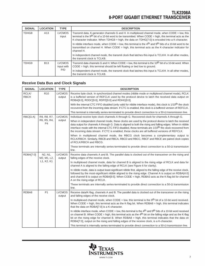
TDHG8 A13 LVCMOSinput
Transmit data, K-generator channels G and H. In multiplexed channel mode, when CODE = low, thisterminal is the 9th bit of a 10-bit word to be transmitted. When CODE = high, this terminal acts as theK-character indicator. When TDHG8 = high, the data on TDHG[7:0] is encoded into a K-character.
In nibble interface mode, when CODE = low, this terminal is the 4th and 9th bits of a 10-bit word to betransmitted on channel H. When CODE = high, this terminal acts as the K-character indicator forchannel H.
In independent channel mode, the transmit clock that latches this input is TCLKH. In all other modes,the transmit clock is TCLKB.
TDHG9 B13 LVCMOSinput with
P/D
Transmit data channels G and H. When CODE = low, this terminal is the 10th bit of a 10-bit word. WhenCODE = high, this terminal should be left floating or tied low to ground.
In independent channel mode, the transmit clock that latches this input is TCLKH. In all other modes,the transmit clock is TCLKB.
Receive Data Bus and Clock Signals
SIGNAL LOCATION TYPE DESCRIPTION
RCLK/RBCH
R10 LVCMOSoutput
Receive byte clock. In synchronized channel modes (nibble mode or multiplexed channel mode), RCLKis a buffered version of REFCLK used by the protocol device to latch the received data output onRDBA[9:0], RDDC[9:0], RDFE[9:0] and RDHG[9:0].
With the internal CTC FIFO disabled (only valid for nibble interface mode), this clock is 1/10th the clockrecovered from the incoming data stream. If CTC is enabled, this clock is a buffered version of REFCLK.
This terminal is internally series-terminated to provide direct connection to a 50-Ω transmission line.
RBC[G:A] R9, R8, R7,R6, R5, R4,
P4
LVCMOSoutput
Individual receive byte clock channels A through G. Recovered clock for channels A through G.
When in independent channel mode, these clocks are used by the protocol device to latch the receiveddata output for channels A through G. Data is aligned to both the rising and falling edges. When in nibbleinterface mode with the internal CTC FIFO disabled, these terminals are 1/10th the clock recovered fromthe incoming data stream. If CTC is enabled, these clocks are all buffered versions of REFCLK.
When in multiplexed channel mode, the RBCG clock becomes a complementary output toRCLK/RBCH. Similarly, RBCB and RBCA, RBCD and RBCC, RBCF and RBCE are paired clock copiesof RCLK/RBCH and RBCG.
These terminals are internally series-terminated to provide direct connection to a 50-Ω transmissionline.
RDBA[7:0] N2, N1,M2, M1, L2,L1, K2, K1
LVCMOSoutput
Receive data channels A and B. The parallel data is clocked out of the transceiver on the rising andfalling edges of the receive clock.
In multiplexed channel mode, data for channel B is aligned to the rising edge of RCLK and data forchannel A is aligned to the falling edge of RCLK (see Figure 6 for clarity).
In nibble mode, data is output least-significant nibble first, aligned to the falling edge of the receive clock,followed by the most-significant nibble aligned to the rising edge. Channel A is output on RDBA[4:0]and channel B is output on RDBA[9:5]. When CODE = high, RDBA3 acts as the K-flag bit for channelA on the rising edge of RCLK.
These terminals are internally series-terminated to provide direct connection to a 50-Ω transmissionline.
RDBA8 P1 LVCMOSoutput
Receive data/K-flag, channels A and B. The parallel data is clocked out of the transceiver on the risingand falling edges of the receive clock.
In multiplexed channel mode, when CODE = low, this terminal is the 9th bit of a 10-bit word received.When CODE = high, this terminal acts as the K-flag bit. When RDBA8 = high, this terminal indicatesthat the data on RDBA[7:0] is a K-character.
In nibble interface mode, when CODE = low, this terminal is the 4th and 9th bits of a 10-bit word receivedon channel B. When CODE = high, this terminal acts as the 4th bit on the falling edge and as the K-flagbit on the rising edge for channel B. When RDBA8 = high, this terminal indicates that the data onRDBA[7:0], output on the rising and falling edges of the receive clock, is a K-character.
This terminal is internally series-terminated to provide direct connection to a 50-Ω transmission line.

8 WWW.TI.COM
DESCRIPTIONTYPELOCATIONSIGNAL
RDBA9 P2 LVCMOSoutput
Receive data 9, channels A and B. The parallel data is clocked out of the transceiver on the rising andfalling edges of the receive clock. In multiplexed channel mode, when CODE = low, this terminal is the10th bit of a 10-bit word received.
In nibble interface mode, when CODE = low, this terminal is the 5th and 10th bits of a 10-bit word receivedon channel B.
This terminal is internally series-terminated-to provide direct connection to a 50-Ω transmission line.
RDDC[7:0] P3, R3, T2,U2, U1, T1,
R2, R1
LVCMOSoutput
Receive data channels C and D. The parallel data is clocked out of the transceiver on the rising andfalling edges of the receive clock.
In multiplexed channel mode, data for channel D is aligned to the rising edge of RCLK and data forchannel C is aligned to the falling edge of RCLK (see Figure 6 for clarity).
In nibble mode, data is output least-significant nibble first, aligned to the falling edge of the receive clock,followed by the most-significant nibble aligned to the rising edge. Channel C is output on RDDC[4:0]and channel D is output on RDDC[9:5]. When CODE = high, RDDC3 acts as the K-flag bit for channelC on the rising edge of RCLK.
These terminals are internally series-terminated to provide direct connection to a 50-Ω transmissionline.
RDDC8 U3 LVCMOSoutput
Receive data/K-flag, channels C and D. The parallel data is clocked out of the transceiver on the risingand falling edges of the receive clock.
In multiplexed channel mode, when CODE = low, this terminal is the 9th bit of a 10-bit word received.When CODE = high, this terminal acts as the K-flag bit. When RDDC8 = high, this terminal indicatesthat the data on RDDC[7:0] is a K-character.
In nibble interface mode, when CODE = low, this terminal is the 4th and 9th bits of a 10-bit word receivedon channel D. When CODE = high, this terminal acts as the 4th bit on the falling edge and as the K-flagbit on the rising edge for channel D. When RDDC8 = high, this terminal indicates that the data onRDDC[7:0], output on the rising and falling edges of the receive clock, is a K-character.
This terminal is internally series-terminated to provide direct connection to a 50-Ω transmission line.
RDDC9 T3 LVCMOSoutput
Receive data 9, channels C and D. The parallel data is clocked out of the transceiver on the rising andfalling edges of the receive clock. In multiplexed channel mode, when CODE = low, this terminal is the10th bit of a 10-bit word received.
In nibble interface mode, when CODE = low, this terminal is the 5th and 10th bits of a 10-bit word receivedon channel D.
This terminal is internally series-terminated to provide direct connection to a 50-Ω transmission line.
RDFE[7:0] T7, U7, T6,U6, T5, U5,
T4, U4
LVCMOSoutput
Receive data channels E and F. The parallel data is clocked out of the transceiver on the rising andfalling edges of the receive clock.
In multiplexed channel mode, data for channel F is aligned to the rising edge of RCLK and data forchannel E is aligned to the falling edge of RCLK (see Figure 6 for clarity).
In nibble mode, data is output least-significant nibble first, aligned to the falling edge of the receive clock,followed by the most-significant nibble aligned to the rising edge. Channel E is output on RDFE[4:0] andchannel F is output on RDFE[9:5]. When CODE = high, RDFE3 acts as the K-flag bit for channel E onthe rising edge of RCLK.
These terminals are internally series-terminated to provide direct connection to a 50-Ω transmissionline.
RDFE8 U8 LVCMOSoutput
Receive data/K-flag, channels E and F. The parallel data is clocked out of the transceiver on the risingand falling edges of the receive clock.
In multiplexed channel mode, when CODE = low, this terminal is the 9th bit of a 10-bit word received.When CODE = high, this terminal acts as the K-flag bit. When RDFE8 = high, this terminal indicatesthat the data on RDFE[7:0] is a K-character.
In nibble interface mode, when CODE = low, this terminal is the 4th and 9th bits of a 10-bit word receivedon channel F. When CODE = high, this terminal acts as the 4th bit on the falling edge and as the K-flagbit on the rising edge for channel F. When RDFE8 = high, this terminal indicates that the data onRDFE[7:0], output on the rising and falling edges of the receive clock, is a K-character.
This terminal is internally series terminated to provide direct connection to a 50-Ω transmission line.
9WWW.TI.COM
DESCRIPTIONTYPELOCATIONSIGNAL
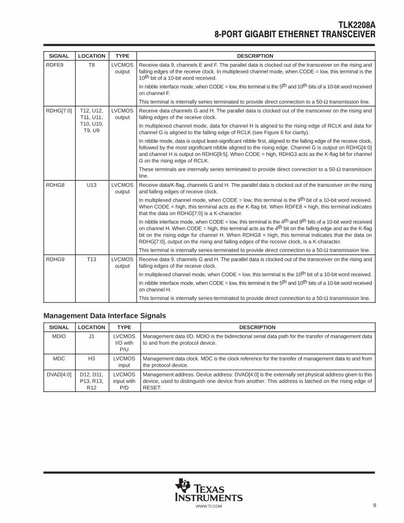
RDFE9 T8 LVCMOSoutput
Receive data 9, channels E and F. The parallel data is clocked out of the transceiver on the rising andfalling edges of the receive clock. In multiplexed channel mode, when CODE = low, this terminal is the10th bit of a 10-bit word received.
In nibble interface mode, when CODE = low, this terminal is the 5th and 10th bits of a 10-bit word receivedon channel F.
This terminal is internally series terminated to provide direct connection to a 50-Ω transmission line.
RDHG[7:0] T12, U12,T11, U11,T10, U10,
T9, U9
LVCMOSoutput
Receive data channels G and H. The parallel data is clocked out of the transceiver on the rising andfalling edges of the receive clock.
In multiplexed channel mode, data for channel H is aligned to the rising edge of RCLK and data forchannel G is aligned to the falling edge of RCLK (see Figure 6 for clarity).
In nibble mode, data is output least-significant nibble first, aligned to the falling edge of the receive clock,followed by the most significant nibble aligned to the rising edge. Channel G is output on RDHG[4:0]and channel H is output on RDHG[9:5]. When CODE = high, RDHG3 acts as the K-flag bit for channelG on the rising edge of RCLK.
These terminals are internally series terminated to provide direct connection to a 50-Ω transmissionline.
RDHG8 U13 LVCMOSoutput
Receive data/K-flag, channels G and H. The parallel data is clocked out of the transceiver on the risingand falling edges of receive clock.
In multiplexed channel mode, when CODE = low, this terminal is the 9th bit of a 10-bit word received.When CODE = high, this terminal acts as the K-flag bit. When RDFE8 = high, this terminal indicatesthat the data on RDHG[7:0] is a K-character.
In nibble interface mode, when CODE = low, this terminal is the 4th and 9th bits of a 10-bit word receivedon channel H. When CODE = high, this terminal acts as the 4th bit on the falling edge and as the K-flagbit on the rising edge for channel H. When RDHG8 = high, this terminal indicates that the data onRDHG[7:0], output on the rising and falling edges of the receive clock, is a K-character.
This terminal is internally series-terminated to provide direct connection to a 50-Ω transmission line.
RDHG9 T13 LVCMOSoutput
Receive data 9, channels G and H. The parallel data is clocked out of the transceiver on the rising andfalling edges of the receive clock.
In multiplexed channel mode, when CODE = low, this terminal is the 10th bit of a 10-bit word received.
In nibble interface mode, when CODE = low, this terminal is the 5th and 10th bits of a 10-bit word receivedon channel H.
This terminal is internally series-terminated to provide direct connection to a 50-Ω transmission line.
Management Data Interface Signals
SIGNAL LOCATION TYPE DESCRIPTION
MDIO J1 LVCMOSI/O with
P/U
Management data I/O. MDIO is the bidirectional serial data path for the transfer of management datato and from the protocol device.
MDC H3 LVCMOSinput
Management data clock. MDC is the clock reference for the transfer of management data to and fromthe protocol device.
DVAD[4:0] D12, D11,P13, R13,
R12
LVCMOSinput with
P/D
Management address. Device address: DVAD[4:0] is the externally set physical address given to thisdevice, used to distinguish one device from another. This address is latched on the rising edge ofRESET.

10 WWW.TI.COM
JTAG Interface Signals
SIGNAL LOCATION TYPE DESCRIPTION
TCK C10 LVCMOSinput
Test clock. IEEE 1149.1 (JTAG) TCK is used to clock state information and test data into and out ofthe device during the operation of the test port.
TDI C9 LVCMOSinput with
P/U
Test data input. IEEE 1149.1 (JTAG) TDI is used to shift test data and test instructions into the deviceserially during the operation of the test port.
TDO C7 LVCMOSoutput
Test data output. IEEE 1149.1 (JTAG) TDO is used to shift test data and test instructions out of thedevice serially during operation of the test port. When the JTAG port is not in use, TDO is in ahigh-impedance state.
TMS C11 LVCMOSinput
with P/U
Test mode select. IEEE 1149.1 (JTAG) TMS is used to control the state of the internal test-portcontroller.
TRST D8 LVCMOSinput
with P/U
JTAG reset. IEEE 1149.1 (JTAG) TRST is used to reset the internal JTAG controller.
Miscellaneous Signals
SIGNAL LOCATION TYPE DESCRIPTION
CODE J2 LVCMOSinput
with P/D
Encode enable. When high, the 8b/10b encoder and decoder are enabled. The logic value of thisterminal is logically ORed with MDIO register 17.7 (8b/10b_EN).
CV_DIS_EN J3 LVCMOSinput
with P/D
Code violation/disparity error code enable. When CV_DIS_EN is high, the outputs RDxx[9:0] areset to 1 when a code violation or disparity error is detected. The logic value of this terminal is logicallyORed with the MDIO register 17.14 (CVDispEn).
This requires CODE to be enabled.
RESET G3 LVCMOSinput with
P/D
Chip reset (FIFO clear). Pulling this terminal high recenters the transmit skew buffers, recentersreceive channel synchronization FIFOs, and resets MDIO flags.
LPBK D7 LVCMOSinput
with P/D
Serial loopback enable. When asserted high, the outputs of the 8b/10b encoder are looped into theinputs of the 8b/10b decoder for each channel. The serial transmit outputs are held in thehigh-impedance state and the serial inputs are ignored. Whenever a channel is switched into or outof LoopBack, that channel should be reset.
MODE1MODE0
P12, P11 LVCMOSinput
with P/D
Configuration terminals. These terminals put the device under one of the following operation modes:
MODE[1:0]00 – Multiplexed channel mode01 – Reserved10 – Nibble interface mode11 – Reserved
ENABLE D13 LVCMOSinput
with P/U
Device enable. Pulling this terminal high enables all outputs of the device. A low on this terminalplaces all outputs for the device in the high-impedance state.
TCLKSEL D9 LVCMOSinput
Transfer clock select. This terminal controls clock selection mode between synchronized andindependent channel mode.
In independent channel mode (TCLKSEL = 1) channels are clocked in and out by independentclocks TLCK[B:H] and RBC[A:H], respectively. In synchronized channel mode (TCLKSEL = 0)transmit and receive clocks are centered around TCLKB and RCLK/RBCH.
The logic value of this signal is ORed with TransClkMode, MDIO register R17.15.
BUSYEN P9 LVCMOSinput
with P/U
Busy mode enable. When asserted high, /K28.5/D10.1/ are treated as valid data and passedthrough the FIFO. When in the low state it causes high /K28.5/D10.1/ to be treated as an IDLEsequence that can be deleted.
PLL_LOCK R11 LVCMOSoutput
PLL lock. When asserted high, this terminal provides an indication that sufficient time has elapsedafter a power-cycle or power-down sequence to ensure that PLLs have achieved lock.

11WWW.TI.COM
GE_MOD C8 LVCMOSinput
Gigabit Ethernet mode. When driven high, the chip:
1) Treats /K28.5/ followed by any valid data character as an IDLE sequence, except that whenBMOD is asserted, the chip treats /K28.5/D10.1/ as described in the BMOD terminal description.
2) Modifies IDLE to correct disparity by substituting /D5.6/ for /D16.2/ in a /K28.5/Dx.y/ transmit IDLEpair.
There is a state machine coded into the IDLE correction logic for each channel of the TLK2208A suchthat whenever there is a stream of two or more consecutive K28.5 codes clocked into the TLK2208Athen the IDLE correction logic is disabled. If there is ever a reason to clock a continuous stream ofK28.5 codes into the transmit side of the TLK2208A, then following that stream of K codes with anytwo D codes will re−enable the IDLE correction circuit and all subsequent IDLE patterns will conformto the IEEE802.3z specification. Note the steady stream of continuous K28.5 codes does notconform to IEEE802.3 protocol.
The logic value of the GE_MOD terminal is ORed with GEMODE register 24.15.
PRBSEN C13 LVCMOSinput
with P/D
PRBS enable. When this terminal is asserted high, the pseudorandom bit stream generator andcomparator circuits are inserted into the transmit and receive data paths on all channels,respectively.
If this terminal is not used it can be tied to the GND reference.
TX+/TX– are transmitting 27−1 PRBS. RX+/RX– are comparing incoming data to an internallygenerated 27−1 PRBS. Results of the RX comparison can be read from the MDIO.
Power and Reference Terminal Descriptions
SIGNAL LOCATION TYPE DESCRIPTION
VDDQ E9, E8, E7, E6, E5, F5, G5,H5, J5, K5, L5, M5, N5, N6,
N7, N8, N9
Supply I/O supply voltage. 1.8 V ±0.2 V or 2.5 V ±0.2 V
VDD E10, E11, E12, N10, N11,N12
Supply Digital logic power. Provides power for all digital circuitry. Nominally 1.8 V
VDDA E13, F13, G13, H13, J13,K13, L13, M13, N13
Supply Analog power. VDDA provides a supply reference for the high-speed analog circuits,receiver and transmitter. Nominally 1.8 V
GROUND
GNDA E14, F14, G14, H14, J16,J17, K14, L14, M14, N14
Ground Analog ground. GNDA provides a ground reference for the high-speed analog circuits,RX and TX.
GND E4, F4, G4, H4, J4, K4, L4,M4, N4, A14, B14, C14,
D14, P14, R14, T14, U14,A17, B17, C17, D17, E17,F17, G17, H17, K17, L17,M17, N17, P17, R17, T17,
U17
Ground Digital logic ground. Provides a ground for the logic circuits and digital I/O buffers.
Reserved and NC Signals
SIGNAL LOCATION TYPE DESCRIPTION
RSVD F3, P7, P8, P10 RSVD Reserved. Terminals available to TI test. These terminals should not be externallyconnected.
NC D4, D5, D6, D10, J14, J15,K3, L3, M3, N3, P5, P6
NC. These signal terminals have no internal connection.
Terminal-to-Signal Map
TERMINALNUMBER
TERMINALFUNCTION MULTIPLEXED CHANNEL MODE
NIBBLE INTERFACE SYNCHRONIZED ANDINDEPENDENT CHANNEL MODES
A1 TDDC3 Transmit bus channel D/C bit 3 Transmit bus channel C bits 8, 3, K-bit
A2 TDDC4 Transmit bus channel D/C bit 4 Transmit bus channel C bits 9, 4

12 WWW.TI.COM
NIBBLE INTERFACE SYNCHRONIZED ANDINDEPENDENT CHANNEL MODESMULTIPLEXED CHANNEL MODE
TERMINALFUNCTION
TERMINALNUMBER
A3 TDDC8 Transmit bus channel D/C bit 8, K-bit Transmit bus channel D bits 8, 3, K-bit
A4 TDFE0 Transmit bus channel F/E bit 0 Transmit bus channel E bits 5, 0
A5 TDFE2 Transmit bus channel F/E bit 2 Transmit bus channel E bits 7, 2
A6 TDFE4 Transmit bus channel F/E bit 4 Transmit bus channel E bits 9, 4
A7 TDFE6 Transmit bus channel F/E bit 6 Transmit bus channel F bits 6, 1
A8 TDFE8 Transmit bus channel F/E bit 8, K-bit Transmit bus channel F bits 8, 3 , K-bit
A9 TDHG0 Transmit bus channel H/G bit 0 Transmit bus channel G bits 5, 0
A10 TDHG2 Transmit bus channel H/G bit 2 Transmit bus channel G bits 7, 2
A11 TDHG4 Transmit bus channel H/G bit 4 Transmit bus channel G bits 9, 4
A12 TDHG6 Transmit bus channel H/G bit 6 Transmit bus channel H bits 6, 1
A13 TDHG8 Transmit bus channel H/G bit 8, K-bit Transmit bus channel H bits 8, 3, K-bit
A14 GNDA Analog ground
A15 TXH– Channel H serial output –
A16 TXH+ Channel H serial output +
A17 GNDA Analog ground
B1 TDDC2 Transmit bus channel D/C bit 2 Transmit bus channel C bits 7, 2
B2 TDDC5 Transmit bus channel D/C bit 5 Transmit bus channel D bits 5, 0
B3 TDDC9 Transmit bus channel D/C bit 9 Transmit bus channel D bits 9, 4
B4 TDFE1 Transmit bus channel F/E bit 1 Transmit bus channel E bits 6, 1
B5 TDFE3 Transmit bus channel F/E bit 3 Transmit bus channel E bits 8, 3, K-bit
B6 TDFE5 Transmit bus channel F/E bit 5 Transmit bus channel F bits 5, 0
B7 TDFE7 Transmit bus channel F/E bit 7 Transmit bus channel F bits 7, 2
B8 TDFE9 Transmit bus channel F/E bit 9 Transmit bus channel F bits 9, 4
B9 TDHG1 Transmit bus channel H/G bit 1 Transmit bus channel G bits 6, 1
B10 TDHG3 Transmit bus channel H/G bit 3 Transmit bus channel G bits 8, 3, K-bit
B11 TDHG5 Transmit bus channel H/G bit 5 Transmit bus channel H bits 5, 0
B12 TDHG7 Transmit bus channel H/G bit 7 Transmit bus channel H bits 7, 2
B13 TDHG9 Transmit bus channel H/G bit 9 Transmit bus channel H bits 9, 4
B14 GNDA Analog ground
B15 TXG– Channel G serial output–
B16 TXG+ Channel G serial output+
B17 GNDA Analog ground
C1 TDDC0 Transmit bus channel D/C bit 0 Transmit bus channel C bits 5, 0
C2 TDDC1 Transmit bus channel D/C bit 1 Transmit bus channel C bits 6, 1
C3 TDDC6 Transmit bus channel D/C bit 6 Transmit bus channel D bits 6, 1
C4 TCLKD Unused Channels C and D transmit bus clock
C5 TCLKF Unused Channels E and F transmit bus clock
C6 TCLKH Unused Channels G and H transmit bus clock
C7 TDO JTAG test data output
C8 GE_MOD Gigabit Ethernet mode
C9 TDI JTAG test data input
C10 TCK JTAG test clock
C11 TMS JTAG mode select
C12 REFCLK Reference clock
C13 PRBSEN 27 − 1 PRBS enable
C14 GNDA Analog ground

13WWW.TI.COM
NIBBLE INTERFACE SYNCHRONIZED ANDINDEPENDENT CHANNEL MODESMULTIPLEXED CHANNEL MODE
TERMINALFUNCTION
TERMINALNUMBER
C15 TXF– Channel F serial output–
C16 TXF+ Channel F serial output+
C17 GNDA Analog ground
D1 TDBA0 Transmit bus channel B/A bit 0 Transmit bus channel A bits 5, 0
D2 TDBA1 Transmit bus channel B/A bit 1 Transmit bus channel A bits 6, 1
D3 TDDC7 Transmit bus channel D/C bit 7 Transmit bus channel D bits 7, 2
D4 NC No connect
D5 NC No connect
D6 NC No connect
D7 LPBK Internal loopback enable
D8 TRST JTAG test reset
D9 TCLKSEL Multiplexed/independent clocking mode selection
D10 NC No connect
D11 DVAD3 MDIO address LSB
D12 DVAD4 MDIO address MSB
D13 ENABLE Device enable
D14 GNDA Analog ground
D15 TXE– Channel E serial output –
D16 TXE+ Channel E serial output +
D17 GNDA Analog ground
E1 TDBA2 Transmit bus channel B/A bit 2 Transmit bus channel A bits 7, 2
E2 TDBA3 Transmit bus channel B/A bit 3 Transmit bus channel A bits 8, 3, K-bit
E3 TCLKB Transmit bus clock
E4 GND Core ground
E5 VDDQ I/O voltage supply
E6 VDDQ I/O voltage supply
E7 VDDQ I/O voltage supply
E8 VDDQ I/O voltage supply
E9 VDDQ I/O voltage supply
E10 VDD Core voltage supply
E11 VDD Core voltage supply
E12 VDD Core voltage supply
E13 VDDA I/O voltage supply
E14 GNDA Analog ground
E15 TXD– Channel D serial output –
E16 TXD+ Channel D serial output +
E17 GNDA Analog ground
F1 TDBA4 Transmit bus channel B/A bit 4 Transmit bus channel A bits 9, 4, K-bit
F2 TDBA5 Transmit bus channel B/A bit 5 Transmit bus channel B bits 5, 0
F3 RSVD Reserved—should be left unconnected
F4 GND Core ground
F5 VDDQ I/O voltage supply
F6 T-GND Thermal ground
F7 T-GND Thermal ground
F8 T-GND Thermal ground
F9 T-GND Thermal ground

14 WWW.TI.COM
NIBBLE INTERFACE SYNCHRONIZED ANDINDEPENDENT CHANNEL MODESMULTIPLEXED CHANNEL MODE
TERMINALFUNCTION
TERMINALNUMBER
F10 T-GND Thermal ground
F11 T-GND Thermal ground
F12 T-GND Thermal ground
F13 VDDA Analog voltage supply
F14 GNDA Analog ground
F15 TXC– Channel C serial output –
F16 TXC+ Channel C serial output +
F17 GNDA Analog ground
G1 TDBA6 Transmit bus channel B/A bit 6 Transmit bus channel B bits 6, 1
G2 TDBA7 Transmit bus channel B/A bit 7 Transmit bus channel B bits 7, 2
G3 RESET Device reset
G4 GND Core ground
G5 VDDQ I/O voltage supply
G6 T-GND Thermal ground
G7 T-GND Thermal ground
G8 T-GND Thermal ground
G9 T-GND Thermal ground
G10 T-GND Thermal ground
G11 T-GND Thermal ground
G12 T-GND Thermal ground
G13 VDDA Analog voltage supply
G14 GNDA Analog ground
G15 TXB– Channel B serial output –
G16 TXB+ Channel B serial output +
G17 GNDA Analog ground
H1 TDBA8 Transmit bus channel B/A bit 8, K bit Transmit bus channel B bits 8, 3, K-bit
H2 TDBA9 Transmit bus channel B/A bit 9 Transmit bus channel B bits 9, 4
H3 MDC MDIO Clock
H4 GND Core ground
H5 VDDQ I/O voltage supply
H6 T-GND Thermal ground
H7 T-GND Thermal ground
H8 T-GND Thermal ground
H9 T-GND Thermal ground
H10 T-GND Thermal ground
H11 T-GND Thermal ground
H12 T-GND Thermal ground
H13 VDDA Analog voltage supply
H14 GNDA Analog ground
H15 TXA– Channel A serial output –
H16 TXA+ Channel A serial output +
H17 GNDA Analog ground
J1 MDIO MDIO data I/O
J2 CODE 8b/10b enable
J3 CV_DIS_EN Code violation enable
J4 GND Core ground

15WWW.TI.COM
NIBBLE INTERFACE SYNCHRONIZED ANDINDEPENDENT CHANNEL MODESMULTIPLEXED CHANNEL MODE
TERMINALFUNCTION
TERMINALNUMBER
J5 VDDQ I/O voltage supply
J6 T-GND Thermal ground
J7 T-GND Thermal ground
J8 T-GND Thermal ground
J9 T-GND Thermal ground
J10 T-GND Thermal ground
J11 T-GND Thermal ground
J12 T-GND Thermal ground
J13 VDDA Analog voltage supply
J14 NC No connect
J15 NC No connect
J16 GNDA Analog ground
J17 GNDA Analog ground
K1 RDBA0 Receive bus channel B/A bit 0 Receive bus channel A bits 5, 0
K2 RDBA1 Receive bus channel B/A bit 1 Receive bus channel A bits 6, 1
K3 NC No connect
K4 GND Core ground
K5 VDDQ I/O voltage supply
K6 T-GND Thermal ground
K7 T-GND Thermal ground
K8 T-GND Thermal ground
K9 T-GND Thermal ground
K10 T-GND Thermal ground
K11 T-GND Thermal ground
K12 T-GND Thermal ground
K13 VDDA Analog voltage supply
K14 GNDA Analog ground
K15 RXH– Channel H serial input –
K16 RXH+ Channel H serial input +
K17 GNDA Analog ground
L1 RDBA2 Receive bus channel B/A bit 2 Receive bus channel A bits 7, 2
L2 RDBA3 Receive bus channel B/A bit 3 Receive bus channel A bits 8, 3, K-bit
L3 NC No connect
L4 GND Core ground
L5 VDDQ I/O voltage supply
L6 T-GND Thermal ground
L7 T-GND Thermal ground
L8 T-GND Thermal ground
L9 T-GND Thermal ground
L10 T-GND Thermal ground
L11 T-GND Thermal ground
L12 T-GND Thermal ground
L13 VDDA Analog voltage supply
L14 GNDA Analog ground
L15 RXG– Channel G serial input –
L16 RXG+ Channel G serial input +
16 WWW.TI.COM
NIBBLE INTERFACE SYNCHRONIZED ANDINDEPENDENT CHANNEL MODESMULTIPLEXED CHANNEL MODE
TERMINALFUNCTION
TERMINALNUMBER
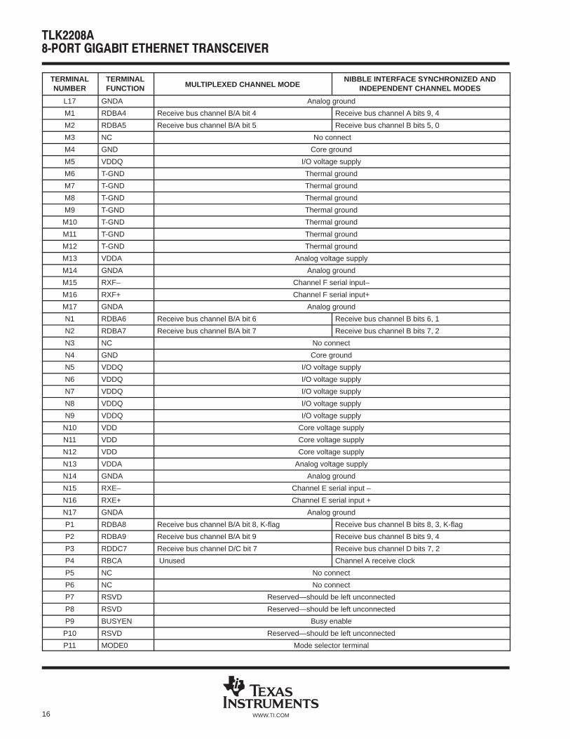
L17 GNDA Analog ground
M1 RDBA4 Receive bus channel B/A bit 4 Receive bus channel A bits 9, 4
M2 RDBA5 Receive bus channel B/A bit 5 Receive bus channel B bits 5, 0
M3 NC No connect
M4 GND Core ground
M5 VDDQ I/O voltage supply
M6 T-GND Thermal ground
M7 T-GND Thermal ground
M8 T-GND Thermal ground
M9 T-GND Thermal ground
M10 T-GND Thermal ground
M11 T-GND Thermal ground
M12 T-GND Thermal ground
M13 VDDA Analog voltage supply
M14 GNDA Analog ground
M15 RXF– Channel F serial input–
M16 RXF+ Channel F serial input+
M17 GNDA Analog ground
N1 RDBA6 Receive bus channel B/A bit 6 Receive bus channel B bits 6, 1
N2 RDBA7 Receive bus channel B/A bit 7 Receive bus channel B bits 7, 2
N3 NC No connect
N4 GND Core ground
N5 VDDQ I/O voltage supply
N6 VDDQ I/O voltage supply
N7 VDDQ I/O voltage supply
N8 VDDQ I/O voltage supply
N9 VDDQ I/O voltage supply
N10 VDD Core voltage supply
N11 VDD Core voltage supply
N12 VDD Core voltage supply
N13 VDDA Analog voltage supply
N14 GNDA Analog ground
N15 RXE– Channel E serial input –
N16 RXE+ Channel E serial input +
N17 GNDA Analog ground
P1 RDBA8 Receive bus channel B/A bit 8, K-flag Receive bus channel B bits 8, 3, K-flag
P2 RDBA9 Receive bus channel B/A bit 9 Receive bus channel B bits 9, 4
P3 RDDC7 Receive bus channel D/C bit 7 Receive bus channel D bits 7, 2
P4 RBCA Unused Channel A receive clock
P5 NC No connect
P6 NC No connect
P7 RSVD Reserved—should be left unconnected
P8 RSVD Reserved—should be left unconnected
P9 BUSYEN Busy enable
P10 RSVD Reserved—should be left unconnected
P11 MODE0 Mode selector terminal
17WWW.TI.COM
NIBBLE INTERFACE SYNCHRONIZED ANDINDEPENDENT CHANNEL MODESMULTIPLEXED CHANNEL MODE
TERMINALFUNCTION
TERMINALNUMBER
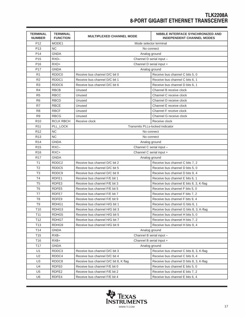
P12 MODE1 Mode selector terminal
P13 NC No connect
P14 GNDA Analog ground
P15 RXD– Channel D serial input –
P16 RXD+ Channel D serial input +
P17 GNDA Analog ground
R1 RDDC0 Receive bus channel D/C bit 0 Receive bus channel C bits 5, 0
R2 RDDC1 Receive bus channel D/C bit 1 Receive bus channel C bits 6, 1
R3 RDDC6 Receive bus channel D/C bit 6 Receive bus channel D bits 6, 1
R4 RBCB Unused Channel B receive clock
R5 RBCC Unused Channel C receive clock
R6 RBCD Unused Channel D receive clock
R7 RBCE Unused Channel E receive clock
R8 RBCF Unused Channel F receive clock
R9 RBCG Unused Channel G receive clock
R10 RCLK RBCH Receive clock Receive clock
R11 PLL_LOCK Transmits PLLs-locked indicator
R12 NC No connect
R13 NC No connect
R14 GNDA Analog ground
R15 RXC– Channel C serial input –
R16 RXC+ Channel C serial input +
R17 GNDA Analog ground
T1 RDDC2 Receive bus channel D/C bit 2 Receive bus channel C bits 7, 2
T2 RDDC5 Receive bus channel D/C bit 5 Receive bus channel D bits 5, 0
T3 RDDC9 Receive bus channel D/C bit 9 Receive bus channel D bits 9, 4
T4 RDFE1 Receive bus channel F/E bit 1 Receive bus channel E bits 6, 1
T5 RDFE3 Receive bus channel F/E bit 3 Receive bus channel E bits 8, 3, K-flag
T6 RDFE5 Receive bus channel F/E bit 5 Receive bus channel F bits 5, 0
T7 RDFE7 Receive bus channel F/E bit 7 Receive bus channel F bits 7, 2
T8 RDFE9 Receive bus channel F/E bit 9 Receive bus channel F bits 9, 4
T9 RDHG1 Receive bus channel H/G bit 1 Receive bus channel G bits 6, 1
T10 RDHG3 Receive bus channel H/G bit 3 Receive bus channel G bits 8, 3, K-flag
T11 RDHG5 Receive bus channel H/G bit 5 Receive bus channel H bits 5, 0
T12 RDHG7 Receive bus channel H/G bit 7 Receive bus channel H bits 7, 2
T13 RDHG9 Receive bus channel H/G bit 9 Receive bus channel H bits 9, 4
T14 GNDA Analog ground
T15 RXB– Channel B serial input –
T16 RXB+ Channel B serial input +
T17 GNDA Analog ground
U1 RDDC3 Receive bus channel D/C bit 3 Receive bus channel C bits 8, 3, K-flag
U2 RDDC4 Receive bus channel D/C bit 4 Receive bus channel C bits 9, 4
U3 RDDC8 Receive bus channel D/C bit 8, K flag Receive bus channel D bits 8, 3, K-flag
U4 RDFE0 Receive bus channel F/E bit 0 Receive bus channel E bits 5, 0
U5 RDFE2 Receive bus channel F/E bit 2 Receive bus channel E bits 7, 2
U6 RDFE4 Receive bus channel F/E bit 4 Receive bus channel E bits 6, 4

18 WWW.TI.COM
NIBBLE INTERFACE SYNCHRONIZED ANDINDEPENDENT CHANNEL MODESMULTIPLEXED CHANNEL MODE
TERMINALFUNCTION
TERMINALNUMBER
U7 RDFE6 Receive bus channel F/E bit 6 Receive bus channel F bits 6, 1
U8 RDFE8 Receive bus channel F/E bit 8, K flag Receive bus channel F bits 8, 3, K-flag
U9 RDHG0 Receive bus channel H/G bit 0 Receive bus channel G bits 5, 0
U10 RDHG2 Receive bus channel H/G bit 2 Receive bus channel G bits 7, 2
U11 RDHG4 Receive bus channel H/G bit 4 Receive bus channel G bits 9, 4
U12 RDHG6 Receive bus channel H/G bit 6 Receive bus channel H bits 6, 1
U13 RDHG8 Receive bus channel H/G bit 8, K flag Receive bus channel H bits 8, 3, K-flag
U14 GNDA Analog ground
U15 RXA– Channel A serial input –
U16 RXA+ Channel A serial input +
U17 GNDA Analog ground
detailed description
reference clock synthesizer
The TLK2208A employs a mature phase-lock loop (PLL) design in use for Gigabit Ethernet transceivers andhigh-speed serial links by Texas Instruments since 1997 on both standard products and custom ASIC designs.This PLL design is used to synthesize the serial line-rate bit clock from the REFCLK input as well as generateclocks for the receiver sampling circuitry. The PLL and associated high-speed circuitry are powered by theanalog power supply terminals (VDDA) with isolated grounds (GNDA). Care should be taken in providing alow-noise environment in a system. It is recommended to supply the VDDA reference by a separate isolatedplane within the system printed-circuit board (PCB). It is recommended that systems employing switching powersupplies provide proper filtering of the fundamental and harmonic components in the 2-MHz–10-MHz band toavoid bit errors from injected noise. It is strongly recommended that no PLL-based clock synthesizer circuit beused as the source for the REFCLK. This could cause accumulation of jitter between the two PLLs.
operating modes
The TLK2208A has two operational modes selectable via the CODE terminal, as detailed in Table 1.
Table 1. Operational Modes
CODE OPERATING MODES
LowSERDES mode. On-chip 8b/10b encoder/decoder is disabled. Refer to the byte alignment logic section, for additional descriptionon control over this mode.
HighTransceiver mode. Enables 8b/10b encode/decode for each channel. Data on the transmit and receive data buses is treated asuncoded data. The K-generator bit is used as the K-character generator control. The K-flag is the K-character indicator to the hostdevice.
NOTE: The logic value of the code terminal is ORed with MDIO register 17.7 (8B/10B_EN).
In SERDES mode, the transmit data bus for each channel accepts 10-bit-wide data on the transmit data channelterminals. Data is latched on the rising and falling edges of the transmit data clock. The data is thenphase-aligned, serialized, and transmitted sequentially beginning with bit 0 over the differential high-speedserial transmit terminals. The receive data bus for each channel outputs 10-bit data. Data is output relative toboth the rising and falling edges of the receive clock.
In transceiver mode, the transmit data bus for each channel accepts 8-bit-wide parallel data. Data is sampledon the rising and falling edges of the transmit clock. The data is first aligned to the reference clock (REFCLK),then 8b/10b encoded and passed to the serializer. The generation of K-characters on each channel is controlledby the K-generator bit (see the parallel interface modes section). When the K-generator bit is asserted alongwith the 8 bits of data, the appropriate 8b/10b K-character is transmitted. The receive data bus for each channel

19WWW.TI.COM
outputs 8-bit-wide parallel data. Reception of K-characters is reported on the K-flag bit (see the parallelinterface modes section). When the K-flag of any channel is asserted, the 8 bits of data on that channel’sreceive data bus should be interpreted as a K-character.
When CV_DIS_EN is high, the outputs RDxx[8:0] are set to 1 when a code violation or RD error is detected.
When CV_DIS_EN is low, the outputs RDxx[7:0] are set to 1 when a code violation is detected. An RD error isnot indicated in this case.
parallel interface modes
The TLK2208A provides two basic operational interface modes controlled by the state of terminals MODE0 andMODE1. The internal state of these mode terminals can be controlled via MDIO to change the modes ofoperation. These operational interface modes are listed in Table 2.
Table 2. Parallel Interface Modes
MODE1 MODE2 OPERATING MODES
Low Low Multiplexed channel mode
Low High Reserved
High Low Nibble interface channel mode
High High Reserved
NOTE: MODE terminals can be overridden via MDIO register 17.6(MODE_OVR).
Regardless of MODE settings, the channels can be operated in synchronous mode or independent mode. Thechannels are operated in synchronous mode when the TCLKSEL terminal (or MDIO register 17.15) is set to alogic low (default). If either the terminal or the MDIO register is set to a logic high, the channels are operatedin independent mode. See the serializer section for further details.
The clock tolerance compensation, (see the clock tolerance compensation (CTC) section), is enabled bydefault and must not be disabled via MDIO while in the multiplexed channel mode.
transmit logic
The transmit logic converts parallel data into an NRZ serial bit stream with a differential VML output at1.0–1.3 Gbps, dependent on REFCLK and TCLKx frequency. The input to the transmitter can be either an 8-bitparallel word plus a control (K) bit, or a 10-bit word.
transmit clock interface
The TLK2208A provides two transmit clocking modes as summarized in Table 3. In synchronous channel mode,all input data for all channels is timed from a single input clock, TCLKB. In independent channel mode, fourclocks are used; input data for each pair of channels is timed with one of these clocks.
In synchronous channel mode, data to be transmitted is latched by both the rising and falling edges of TCLKB.TCLKB must be frequency synchronous with REFCLK (0 ppm), but may have any phase relationship withrespect to REFCLK.
In independent channel mode, input data for channels A and B is referenced from TCLKB. Input data forchannels C and D is referenced from TCLKD. Input data for channels E and F is referenced from TCLKF, andlastly input data from channels G and H is referenced from TCLKH. TCLKB, TCLKD, TCLKF and TCLKH areexpected to be the same frequency as the reference clock, REFCLK, but of arbitrary phase.

20 WWW.TI.COM
Table 3. Independent vs Synchronous Mode
TCLKSEL(TERMINAL)
TransClkModeMDIO
REGISTER17.15
OPERATING MODE
Low Low Synchronous channel mode
Don’t Care High Independent channel mode
High Don’t Care Independent channel mode

21WWW.TI.COM
transmit logic (continued)
transmit parallel interface
The TLK2208A provides source-centered interface to the MAC.
In multiplexed channel mode, channels A and B, C and D, E and F, and G and H are each interleaved on thesame 10-bit bus. Channels B, D, F, H are input referenced to the rising edge of TCLKx. Channels A, C, E, andG are input referenced to the falling edge of TCLKB (see Figure 4).
CH[G,E,C,A]
TCLKx
Source CenteredTDxx[9:0]
CH[H,F,D,B]
Figure 4. Multiplexed Channel Transmit Timing Options
In the nibble interface mode, channels B, D, F, and H are input on high-order nibble TDxx[9:5], while channelsA, C, E, and G are input on low-order nibble TDxx[4:0], as shown in Figure 5. Note: In the transmit direction,channel pairs (A/B, C/D, E/F, G/H) have a common transmit clock and DDR input register bank. As a result,software assertion of the Channel A TX_SwRST MDIO register will temporarily corrupt Channel B data (untilthe software reset ends). Channel C TX_SwRST causes the same data corruption on Channel D. Channel ETX_SwRST causes the same data corruption on Channel F. Channel G TX_SwRST causes the same datacorruption on Channel H.
CH[A,C,E,G]Least-Significant
Nibble
TCLKx
Source CenteredTDxx[4:0]
TDxx[9:5]
CH[A,C,E,G]Most-Significant
Nibble
CH[B,D,F,H]Least-Significant
Nibble
CH[B,D,F,H]Most-Significant
Nibble
Figure 5. Nibble Mode Transmit Timing Options

22 WWW.TI.COM
transmit logic (continued)
8b/10b encoder
All true serial interfaces require a method of encoding to ensure sufficient transition density for the receivingPLL to acquire and maintain lock. The encoding scheme also maintains the signal dc balance by keeping thenumber of 1s and 0s the same, which allows for ac-coupled data transmission. The TLK2208A uses the 8b/10bencoding algorithm that is used by the Fibre Channel and Gigabit Ethernet specifications. This provides goodtransition density for clock recovery and improves error checking. The 8b/10b encoder/decoder function isenabled for all channels by the assertion of the CODE terminal. When enabled, the TLK2208A internallyencodes and decodes the data such that the user actually reads and writes 8-bit data on each channel.
When enabled (CODE = high), the 8b/10b encoder converts 8-bit-wide data to a 10-bit-wide encoded datacharacter to improve its transition density. This transmission code includes D-characters, used for transmittingdata, and K-characters, used for transmitting protocol information. Each K- or D-character code word can alsohave either a positive or a negative disparity version. The disparity of a code word is selected by the encoderto balance the running disparity of the serialized data stream.
The generation of K-characters to be transmitted on each channel is controlled by TDxx8 when in themultiplexed channel mode. When these terminals are asserted along with the 8 bits of data, an 8b/10bK-character is transmitted. Similarly, reception of K-characters is reported by RDxx8. When RDxx8 is asserted,the 8 bits of data on RDxx should be interpreted as a K-character. The TLK2208A transmits and receives all12 of the valid K-characters defined in the Fibre Channel and Gigabit Ethernet specifications. Invalid datapatterns input when TDxx8 is asserted result in an invalid K-character being transmitted, which results in ancode error at the receiver.
serializer
The parallel-to-serial shift register on each channel takes in 10-bit wide data from either the 8b/10b encoders,if enabled, or directly from the transmit data bus, and converts it to a serial stream. The shift register is clockedby the internally generated bit clock, which is 10 times the reference-clock (REFCLK) frequency. Theleast-significant bit (LSB) for each channel is transmitted first.
receive logic
The receiver input data must be ac-coupled and have a rate of 1.0–1.3 Gbps. Resistive termination to match50-Ω traces is on-chip. The clock recovery circuitry retimes the input data by extracting a clock from the inputdata, and passes on the serial data and this recovered clock to the deserializer. Byte alignment is performedon K-characters per IEEE 802.3z (see the byte alignment logic section for details).
receive parallel interface
The receive data bus for all channels is output source centered with the bus clock in the center of the data eye,allowing direct connection to the protocol device.
In multiplexed channel and nibble interface synchronized channel modes, parallel data to be transferred to theprotocol device is output referenced to both the rising and falling edges of RCLK. RCLK is frequencysynchronous with REFCLK, but has no set phase relationship with respect to REFCLK.
In multiplexed channel mode, channels A and B, C and D, E and F, and G and H are each paired and interleavedon the same 10-bit bus. Channels B, D, F, and H are output referenced to the rising edge of RCLK/RBCH andfalling edge of RBCG (see Figure 6). Channels A, C, E, and G are output referenced to the falling edge ofRCLK/RBCH and rising edge of RBCG. Remaining clocks RBCE−RBCF, RBCC−RBCD, and RBCA−RBCB areidentical copies of RCLK/RBCH–RBCG and could be used as complementary clock pairs.

23WWW.TI.COM
receive logic (continued)
CH[H,F,D,B]
RBCG
RDxx[9:0] CH[G,E,C,A]
RCLK/RBCH
NOTE: RX timing is always source centered.
Figure 6. Multiplexed Channel Receive Timing
In the nibble interface channel mode, channels B, D, F, and H are output on the high-order nibble RDxx[9:5],while channels A, C, E, and G are output on the low-order nibble RDxx[4:0] as shown in Figure 7.
In the nibble interface channel mode, parallel data to be transferred to the protocol device on channel A(RDBA[4:0]) is output referenced to both the rising and falling edges of RBCA, and channel B (RDBA[9:5]) isoutput referenced to both the rising and falling edges of RBCB. Channels C through H are output the same waywith their respective clocks.
CH[A,C,E,G]Most-Significant
Nibble
CH[B,D,F,H]Most-Significant
Nibble
CH[A,C,E,G]Least-Significant
Nibble
RCLK/RBCH, RBCx
RDxx[4:0]
CH[B,D,F,H]Least-Significant
NibbleRDxx[9:5]
NOTE: RX timing is always source centered.
Figure 7. Nibble Mode Receive Timing
clock recovery
A baud-rate clock is extracted from the 10-bit encoded serial data stream independently on each channel. Thereceive clock locks to the input within 2 µs after a valid input data stream is applied. The received data isdeserialized and byte aligned. In the absence of input data, the clock recovery circuit locks onto the referenceclock frequency REFCLK.
deserializer
For each channel, serial data is received on the RXx+/RXx– terminals. The interpolator and clock recoverycircuit locks to the data stream if the clock to be recovered is within ±100 ppm of the internally generated bit-rateclock. The recovered clock is used to retime the input data stream. The serial data is then clocked into theserial-to-parallel shift registers. If enabled, the 10-bit-wide parallel data is then fed into 8b/10b decoders. Theparallel data for each channel is fed into a FIFO buffer where the output is synchronized to REFCLK.

24 WWW.TI.COM
receive logic(continued)
clock tolerance compensation (CTC)
The TLK2208A compensates for the possibility that the incoming serial-data rate on any channel can be asmuch as 100 ppm faster or slower than the REFCLK frequency (±100 ppm). Each channel independently anddynamically compensates for any frequency difference by the use of an elasticity buffer. If the incoming datarate is faster than the REFCLK frequency, the elasticity buffer fills. As it approaches the fill limit, it deletes ordrops a 20-bit IDLE code[1] found in the gap between Ethernet packets. If the incoming data rate is slower thanthe REFCLK, the elasticity buffer empties. As it approaches the empty limit, it adds or inserts a selectable 20-bitIDLE code found in the gap between Ethernet packets. IDLE code selection defaults to IDLE2, and can bechanged to IDLE1 via MDIO. No running disparity is affected due to either the addition or the deletion of the IDLEcode, as the IDLE code has a balanced number of 1s and 0s. Note that a deletion of a 20-bit IDLE code couldreduce the inter-packet gap below the minimum inter-packet gap of 12 bytes (120 bits).
The CTC function adds or deletes IDLE codes only in the interpacket gap or during autonegotiation. Thus, theCTC FIFO depth is set to ensure that maximum size Ethernet packets (1540 bytes) can be receivedcontinuously at the frequency offset extremes without loss of data or synchronization. The CTC function canbe disabled chip-wide via the MDIO registers.
When the CTC function is enabled, recovered clocks (RBCx) are buffered versions of the REFCLK.
When the CTC function is not enabled (nibble mode operation only), the recovered clocks for each channel areone tenth the rate of the clock recovered from the incoming stream.
byte alignment logic
Under default conditions, the TLK2208A uses the IEEE 802.3z-defined 10-bit K28.5 character (commacharacter, positive disparity) word alignment scheme[2]. The following sections explain how this scheme worksand how it realigns itself.
When parallel data is clocked into a parallel-to-serial converter, the byte boundary that was associated with theparallel data is lost in the serialization of the data. When the serial data is received and converted to parallelformat again, a method is needed to be able to recognize the byte boundary again. Generally this isaccomplished through the use of a synchronization pattern. This is a unique a pattern of 1s and 0s that eithercannot occur as part of valid data or is a pattern that repeats at defined intervals. 8b/10b encoding contains acharacter called the comma (001 1111b), which is used by the comma-detect circuit to align the received serialdata back to its original byte boundary. The decoder detects the K28.5 comma, generating a synchronizationsignal aligning the data to their 10-bit boundaries for decoding. It then converts the data back into 8-bit data.It is important to note that the comma can be either 001 1111b or the inverse, 110 0000b, depending on therunning disparity. The TLK2208A decoder detects only the 001 1111b pattern. Therefore, since synchronizationis achieved on the positive comma, two consecutive K-codes containing commas are required to ensure byteboundary synchronization (see Table 4).
During all operations, the TLK2208A receive clocks (RCLK, RBCx) are a constant duty cycle and frequency.There are no stretched or shortened clock pulses.
[1] IEEE 802.3z specifies an IDLE as a 20-bit code consisting of an IDLE1 code (/K28.5/D5.6/) and an IDLE2 code (/K28.5/D16.2/).[2] Setting COMMA_DET = 0 by changing its value via MDIO 17.8 disables comma detection, and byte alignment takes place on any bit boundary; this permits external byte alignment on different bit sequences, and allows for the use of different bit-balancing algorithms.

25WWW.TI.COM
receive logic(continued)
Table 4. Valid K-Characters
RECEIVE DATA BUSENCODED K-CODE
K-CHARACTERRECEIVE DATA BUS
(RDxx[7:0]) NEGATIVE RUNNINGDISPARITY
POSITIVE RUNNINGDISPARITY
K28.0 0001 1100 00 1111 0100 11 0000 1011
K28.1 0011 1100 00 1111 1001[1] 11 0000 0110
K28.2 0101 1100 00 1111 0101 11 0000 1010
K28.3 0111 1100 00 1111 0011 11 0000 1100
K28.4 1001 1100 00 1111 0010 11 0000 1101
K28.5 1011 1100 00 1111 1010[1] 11 0000 0101
K28.6 1101 1100 00 1111 0110 11 0000 1001
K28.7 1111 1100 00 1111 1000[1] 11 0000 0111
K23.7 1111 0111 11 1010 1000 00 0101 0111
K27.7 1111 1011 11 0110 1000 00 1001 0111
K29.7 1111 1101 10 1110 1000 01 0001 0111
K30.7 1111 1110 01 1110 1000 10 0001 0111
NOTE 1: A comma is contained within this K-code.
decoder and code violation logic
When the on-chip 8b/10b encoder/decoder is enabled (CODE = high), the reception of K-characters is reportedby the assertion of RDxx8 on each channel. When a code-word error or running-disparity error is detected inthe decoded data on a channel, RDxx[7:0] is asserted and is all 1s (0xFF).
control logic
MDIO management interface
The TLK2208A supports the management-data input/output (MDIO) interface as defined in Clause 22 of theIEEE 802.3 Ethernet specification. The MDIO allows register-based management and control of the serial links.Normal operation of the TLK2208A is possible without use of this interface because all of the essential signalsnecessary for operations are accessible via the device terminals. However, some additional features areaccessible only through the MDIO.
The MDIO management interface consists of a bidirectional data path (MDIO) and a clock reference (MDC).The timing required to read from the internal registers is shown in Figure 8; the timing required to write to theinternal registers is shown in Figure 9.
MDC
A4MDIO A0 R4 R00110 0Hi-Z
D15 D032 1s
Preamble
SFD
Read Code
PHY Address
Turn Around
Register Address
Data Idle
Figure 8. Management Interface Read Timing

26 WWW.TI.COM
MDIO management interface (continued)
MDC
A4MDIO A0 R4 R01010 0 D15 D032 1s
Preamble
SFD
Write Code
PHY Address
Turn Around
Register Address
Data Idle
1
Figure 9. Management Interface Write Timing
The MDIO interface allows up to 32 (16-bit) internal registers. Sixteen registers are defined in Clause 22 of theIEEE 802.3 specification. Additional registers are allowed for expanded functionality. The TLK2208Aimplements five IEEE-defined registers. The TLK2208A also implements additional registers for expandedfunctionality. The IEEE-defined registers and the expanded functionality registers are outlined in Table 5.
Table 5. MDIO Registers
REGISTERADDRESS REGISTER NAME DEFINITION
0 Control IEEE 802.3-defined. See Table 6.
1 Status IEEE 802.3-defined. See Table 7.
2,3 PHY identifier IEEE 802.3-defined. See Table 8 and Table 9.
4−14 Not applicable
15 Extended status IEEE 802.3-defined. See Table 10.
16 Control register 0 Channel enable controls. See Table 11.
17 Control register 1 Various global controls. See Table 12.
18 Control register 2 Channels [A:B] preemphasis controls. See Table 13.
19 Control register 3 Channels [C:D] preemphasis controls. See Table 14.
20 Control register 4 Channels [E:F] preemphasis controls. See Table 15.
21 Control register 5 Channels [G:H] preemphasis controls. See Table 16.
22 Loopback control Individual channel loopback controls. See. Table 17.
23 Reserved Reserved control/status register. See Table 18.
24 Control register 6 Various global controls, preemphasis PRBS, CTC, busy. See Table 19.
25 Reserved Reserved control/status register. See Table 20.
26 Status register 0 TI test individual channel status. See Table 21.
27 Status register 1 TI test individual channel status. See Table 22.
28 Status register 2 TI PRBS test status. See Table 23.
29 Status register 3 TI test register. See Table 24.
30 Test register 1 TI test control register. See Table 25.
31 Test register 2 TI test reserved register. See Table 26.

27WWW.TI.COM
Table 6. Control Register (0x00) Bit Definitions
BIT(S)DEFAULT
VALUE = 0x0140 NAME DESCRIPTION READ/WRITE
0.15 0b Reset Logically ORed with the logic value of the RESET terminal. Afterthe reset bit is set to one, it automatically sets itself back to zeroon the next MDC clock cycle.1 = Global resets including FIFO clear0 = Normal operation (default)
Read/write,self-clearing
0.14 0b Loopback Logically ORed with the logic value of the LPBK terminal1 = Enable loopback mode on all channels0 = Disable loopback mode on all channels (default)
Read/write
0.13 0b Speed selection (LSB) Not applicable. Read returns a 0. Read-only,See Note 2
0.12 0b Auto-negotiation enable Not applicable. Read returns a 0. Read-only,See Note 2
0.11 0b Power down Setting this bit high powers down the device, with the exceptionthat the MDIO interface stays active.1 = Power-down mode is enabled0 = Normal operation (default)
Read/write
0.10 0b Isolate Not applicable. Read returns a 0. Read-only,See Note 2
0.9 0b Restart auto-negotiation Not applicable. Read returns a 0. Read-only,See Note 2
0.8 1b Duplex mode Only full duplex is supported, Write is ignored, read returns a 1. Read-only,See Note 2
0.7 0b Collision test Not applicable. Read returns a 0. Read-only,See Note 2
0.6 1b Speed selection (MSB) Not applicable. Read returns a 1. Read-only,See Note 2
0.5:0 00 0000b Reserved Read returns 0s, write is ignored. Read-only,See Note 2
NOTE 2: Writing to this bit position is ignored.
Table 7. Status Register (0x01) Bit Definitions
BIT(S)DEFAULT
VALUE = 0x0101 NAME DESCRIPTION READ/WRITE
1.15:9 0000 000b Read returns a 0. Read-only
1.8 1b Extended status Read returns a 1, indicating extended status information is heldin register 0x0F.
Read-only
1.7 0b Reserved Read returns a 0. Read-only
1.6:3 0b Various configurations Read returns a 0. Read-only
1.2 0b Link status Read returns a 0. Read-only
1.1 0b Jabber detect Read returns a 0. Read-only
1.0 1b Extended capability Read returns a 1, indicating extended register capability. Read-only
The identifier code is composed of bits 3−24 of the 25-bit organizationally unique identifier (OUI) assigned toTexas Instruments by the IEEE. The 6-bit manufacturer model number is unique to the TLK2208A. Themanufacturer revision number denotes the current revision of the TLK2208A. See Table 8 and Table 9.

28 WWW.TI.COM
Table 8. PHY ID0 Identifier (0x02) Bit Definitions
OUI ADDRESS BITS 3−18
2.15 2.14 2.13 2.12 2.11 2.10 2.9 2.8 2.7 2.6 2.5 2.4 2.3 2.2 2.1 2.0
0 1 0 0 0 0 0 0 0 0 0 0 0 0 0 0
Table 9. PHY ID1 Identifier (0x03) Bit Definitions
OUI ADDRESS BITS 19−24 MANUFACTURER MODEL NUMBERMANUFACTURER REVISION
NUMBER
3.15 3.14 3.13 3.12 3.11 3.10 3.9 3.8 3.7 3.6 3.5 3.4 3.3 3.2 3.1 3.0
0 1 0 1 0 0 0 0 0 0 1 0 0 0 0 0
Table 10. Extended Status Register (0x0F) Bit Definitions
BIT(S)DEFAULT
VALUE = 0x0000 NAME DESCRIPTION READ/WRITE
15.15:12 0h Various configurations Read returns 0s; write is ignored. Read-only
15.11:0 000h Reserved Read returns 0s; write is ignored. Read-only
Table 11. Control Register 0 (0x10) Bit Definitions
BIT(S)DEFAULT
VALUE = 0xFF00 NAME DESCRIPTION READ/WRITE
16.15:8 FFh CH_Enable[H:A] Channel enable (active high). These bits enable each channelindividually. These bits are initialized to 0xFF when reset. Theseregister bits are ANDed with the logic value of the ENABLE terminal.
Read/write,See Note 3
16.7:0 00h Reserved Read returns 0s; write is ignored. Read-only
NOTE 3: Dynamic changes to these register bits might affect other active ports in operation.

29WWW.TI.COM
Table 12. Control Register 1 (0x11) Bit Definitions
BIT(S)DEFAULT
VALUE= 0x4380 NAME DESCRIPTION READ/WRITE
17.15 0b TransClkMode A logic 0 sets all channels synchronous to TCLKB, a logic 1 setsindividual clocking. This register bit is logically ORed with the logicvalue of the TCLKSEL input terminal.
Read/write
17.14 1b CVDispEn Code-violation and disparity-error global enable. This bit is logicallyORed with the logic value of the CV_DIS_EN terminal.
Read/write
17.13:10 0000b Reserved Read returns a 0; write is ignored.
17.9 1b OUT_EN Global internal parallel output enable (enable = 1).This bit is ANDedwith the logic value of the ENABLE terminal.
Read/write
17.8 1b COMMA_DET Enables comma detect global enable for channel alignment Read/write
17.7 1b 8B/10B_EN Global 8b/10b enable (logically ORed with the logic value of theCODE terminal)
Read/write
17.6 0b MODE_OVR If set to a logic 1, it permits mode override. Read/write
17.5:4 00b MODE[1:0] If MODE_OVR is set, permits override of external terminals for modesetting
Read/write
17.3 0b S_RESET Soft reset (active high). This bit resets all logic in the receive andtransmit sections and in the FIFO. Note that the desertion sequenceof the reset bits is critical to achieving deterministic operation.Performs similarly to the RESET terminal but does not reset MDIOregisters.
Read/write,Self-clearing,See Note 4
17.2:0 000b Reserved Read returns 0s; write is ignored. Read-only
NOTE 4: After the S_RESET bit is set to 1, it automatically sets itself back to 0 on the next MDC clock cycle.
Table 13. Control Register 2 (0x12) Bit Definitions
BIT(S)DEFAULT
VALUE = 0x0DBC NAME DESCRIPTION READ/WRITE
18.15:12 0h Reserved Read returns 0s; write is ignored. Read-only
18.11:10 11b PreEmpAB[1:0] Preemphasis control, channels A and B[00] No preemphasis[01] Low preemphasis[10] Mid preemphasis[11] High preemphasis
Read/write
18.9 0b EdgeOvrCtlAB Overrides global preemphasis settings for channels A and B whenasserted
Read/write
18.8:0 1 1011 1100b IDLE1[8:0] First IDLE character. Default is K28.5. Read/write
Table 14. Control Register 3 (0x13) Bit Definitions
BIT(S)DEFAULT
VALUE = 0x0C50 NAME DESCRIPTION READ/WRITE
19.15:12 0h Reserved Read returns 0s; write is ignored. Read-only
19.11:10 11b PreEmpCD[1:0] Preemphasis control, channels C and D[00] No preemphasis[01] Low preemphasis[10] Mid preemphasis[11] High preemphasis
Read/write
19.9 0b EdgeOvrCtlCD Overrides global preemphasis settings for channels C and D whenasserted
Read/write
19.8:0 0 0101 0000b IDLE2[8:0] Second IDLE character. Default is D16.2. Read/write

30 WWW.TI.COM
Table 15. Control Register 4 (0x14) Bit Definitions
BIT(S)DEFAULT
VALUE = 0x0DBC NAME DESCRIPTION READ/WRITE
20.15:12 0h Reserved Read returns 0s; write is ignored. Read-only
20.11:10 11b PreEmpEF[1:0] Preemphasis control, channels E and F[00] No preemphasis[01] Low preemphasis[10] Mid preemphasis[11] High preemphasis
Read/write
20.9 0b EdgeOvrCtlEF Overrides global preemphasis settings for channels E and F whenasserted
Read/write
20.8:0 1 1011 1100b IDLE1a[8:0] First alternate IDLE character. Default is K28.5. Read/write
Table 16. Control Register 5 (0x15) Bit Definitions
BIT(S)DEFAULT
VALUE = 0x0C50 NAME DESCRIPTION READ/WRITE
21.15:12 0h Reserved Read returns 0s; write is ignored. Read-only
21.11:10 11b PreEmpGH[1:0] Preemphasis control, channels G and H[00] No preemphasis[01] Low preemphasis[10] Mid preemphasis[11] High preemphasis
Read/write
21.9 0b EdgeOvrCtlGH Overrides global preemphasis settings for channels G and H whenasserted
Read/write
21.8:0 0 0101 0000b IDLE2a[8:0] Second alternate IDLE character. Default is K16.2. Read/write
Table 17. Loopback Control Register (0x16) Bit Definitions
BIT(S)DEFAULT
VALUE = 0x0000 NAME DESCRIPTION READ/WRITE
22.15:8 00h LOOPBACK[H:A] Serial loopback enable (active high)
When asserted high, TX[9:0] data is looped back to RX[9:0], utilizingthe value of the CODE (and 8B/10B_EN) selection to steer the datapath. The serial transmit outputs are held in the high-impedance stateand the serial inputs are ignored.
All bits are logically ORed with the logic value of the LPBK terminal.
Read/write
22.7:0 00h SLOOPBACK[H:A] Far end loopback enable (active high) channels H:A.
Input is received at RX+/RX− inputs, deserialized and steered totransmit path, and serialized to TX+/TX− outputs.
Note: This is only valid for channel pairs A and B, C and D, E and Fand G and H.
Read/write
Table 18. Control Register (0x17) Bit Definitions
BIT(S)DEFAULT
VALUE = 0x0C50 NAME DESCRIPTION READ/WRITE
23.15:0 0000h Reserved Read returns 0s. Read-only
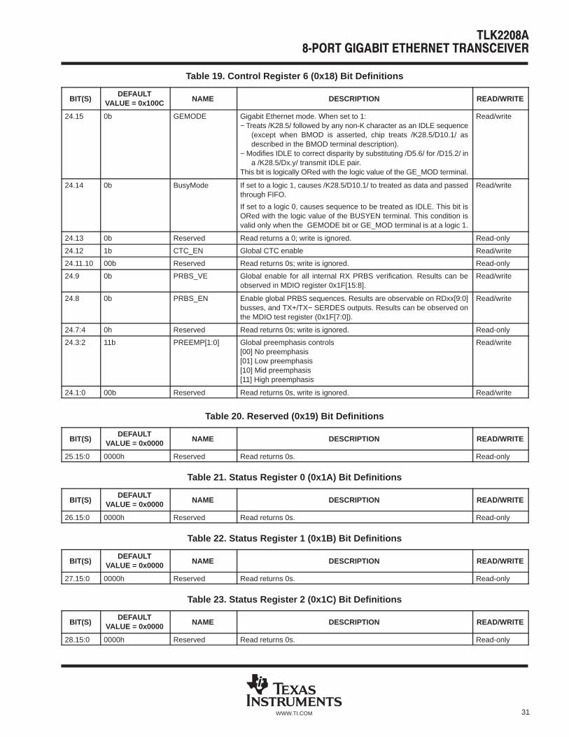
31WWW.TI.COM
Table 19. Control Register 6 (0x18) Bit Definitions
BIT(S)DEFAULT
VALUE = 0x100C NAME DESCRIPTION READ/WRITE
24.15 0b GEMODE Gigabit Ethernet mode. When set to 1:− Treats /K28.5/ followed by any non-K character as an IDLE sequence
(except when BMOD is asserted, chip treats /K28.5/D10.1/ asdescribed in the BMOD terminal description).
− Modifies IDLE to correct disparity by substituting /D5.6/ for /D15.2/ ina /K28.5/Dx.y/ transmit IDLE pair.
This bit is logically ORed with the logic value of the GE_MOD terminal.
Read/write
24.14 0b BusyMode If set to a logic 1, causes /K28.5/D10.1/ to treated as data and passedthrough FIFO.
If set to a logic 0, causes sequence to be treated as IDLE. This bit isORed with the logic value of the BUSYEN terminal. This condition isvalid only when the GEMODE bit or GE_MOD terminal is at a logic 1.
Read/write
24.13 0b Reserved Read returns a 0; write is ignored. Read-only
24.12 1b CTC_EN Global CTC enable Read/write
24.11.10 00b Reserved Read returns 0s; write is ignored. Read-only
24.9 0b PRBS_VE Global enable for all internal RX PRBS verification. Results can beobserved in MDIO register 0x1F[15:8].
Read/write
24.8 0b PRBS_EN Enable global PRBS sequences. Results are observable on RDxx[9:0]busses, and TX+/TX− SERDES outputs. Results can be observed onthe MDIO test register (0x1F[7:0]).
Read/write
24.7:4 0h Reserved Read returns 0s; write is ignored. Read-only
24.3:2 11b PREEMP[1:0] Global preemphasis controls[00] No preemphasis[01] Low preemphasis[10] Mid preemphasis[11] High preemphasis
Read/write
24.1:0 00b Reserved Read returns 0s, write is ignored. Read/write
Table 20. Reserved (0x19) Bit Definitions
BIT(S)DEFAULT
VALUE = 0x0000 NAME DESCRIPTION READ/WRITE
25.15:0 0000h Reserved Read returns 0s. Read-only
Table 21. Status Register 0 (0x1A) Bit Definitions
BIT(S)DEFAULT
VALUE = 0x0000 NAME DESCRIPTION READ/WRITE
26.15:0 0000h Reserved Read returns 0s. Read-only
Table 22. Status Register 1 (0x1B) Bit Definitions
BIT(S)DEFAULT
VALUE = 0x0000 NAME DESCRIPTION READ/WRITE
27.15:0 0000h Reserved Read returns 0s. Read-only
Table 23. Status Register 2 (0x1C) Bit Definitions
BIT(S)DEFAULT
VALUE = 0x0000 NAME DESCRIPTION READ/WRITE
28.15:0 0000h Reserved Read returns 0s. Read-only

32 WWW.TI.COM
Table 24. Status Register 3 (0x1D) Bit Definitions
BIT(S)DEFAULT
VALUE = 0x0000 NAME DESCRIPTION READ/WRITE
29.15:8 00h RX_SwRst[7:0] Individual receive channel resetResets channel when set to logic high
Read/write,self-clearing,See Note 5
29.7:0 00h TX_SwRst[7:0] Individual transmit channel resetResets channel when set to logic high
Read/write,self-clearing,See Note 5
NOTE 5: After these bits are set to 1, they automatically set themselves back to 0 on the next MDC clock cycle. Note: In the transmit direction,channel pairs (A/B, C/D, E/F, G/H) have a common transmit clock and DDR input register bank. As a result, software assertion of theChannel A TX_SwRST MDIO register will temporarily corrupt Channel B data (until the software reset ends). Channel C TX_SwRSTcauses the same data corruption on Channel D. Channel E TX_SwRST causes the same data corruption on Channel F. Channel GTX_SwRST causes the same data corruption on Channel H.
Table 25. Test Register 1 (0x1E) Bit Definitions
BIT(S)DEFAULT
VALUE = 0x000B NAME DESCRIPTION READ/WRITE
30.15:8 00h TI_TST[7:0] Reserved for TI testing Read/write
30.7 0b Reserved Reserved for TI testing Read-only
30.6 0b ASYPHRCTL Reserved for TI testing Read/write
30.5 0b BCLK_RST Reserved for TI testing Read/write
30.4 0b TCLK_EN Reserved for TI testing Read/write
30.3 1b LOCK2RX Reserved for TI testing Read/write
30.2 0b PHRPOL Reserved for TI testing Read/write
30.1:0 11b PHRMAG[1:0] Reserved for TI testing Read/write
Table 26. Test Register 1 (0x1F) Bit Definitions
BIT(S)DEFAULT
VALUE = 0x0000 NAME DESCRIPTION READ/WRITE
31.15:8 00h RX PRBS_Pass[H:A] PRBS pass information for all RX channels H through A Read-only
31.7:0 00h TX PRBS_Pass[H:A] PRBS pass information for all TX channels H through A (reservedfor TI testing)
Read-only
JTAG interface
The TLK2208A provides the full five-terminal JTAG interface as defined in IEEE 1149.1 to supportmanufacturing test.
serial loopback
The TLK2208A can provide a self-test function by enabling the internal serial loopback path for all channels withthe assertion of LPBK. The loopback for individual channels can be enabled via the MDIO registers (22.15:8).The parallel data output can be compared to the parallel input data for that channel to perform functionalverification. The external differential output is held in a high-impedance state during the serial loopback testing.Incoming data on the serial interface is disregarded.
Whenever a channel is switched into or out of LoopBack, that channel should be reset. The circuitry thatswitches the internal clock to the receive path does not preclude the possibility of glitches or short clock cycleswhen the TLK2208A is switched into or out of LoopBack. It is expected that whenever a channel of theTLK2208A is switched into LoopBack that that channel will be reset after making the switch. Also, it is expectedthat whenever a channel of the TLK2208A is switched out of LoopBack that that channel will be reset aftermaking the switch.

33WWW.TI.COM
This recommendation applies whether the LoopBack mode is enabled by way of the LPBK pin (ball D7) or byway of the MDIO register bits.
far-end loopback
The TLK2208A can provide a self-test function by enabling the internal far-end loopback path for all or pairs ofchannels with the assertion of MDIO register bits 22.7:0. The serial data output can be compared to the serialinput data for selected channels to perform functional verification of high-speed RX and TX. The parallel inputdata during the far-end loopback test is disregarded. The external parallel outputs are held in a high-impedancestate during the far-end loopback testing.
power-on reset
Upon application of minimum valid power, the TLK2208A generates an internal power-on reset. During thepower-on reset the receive data outputs are placed in the high-impedance state and the recovered receive clockterminals are held low. The length of the power-on reset cycle is dependent upon the ramp curve of the powersupply . A typical value would be 1 ms after VDD crosses Vth (approx. 1/2 VDD). The power-on reset is sourcedby the digital core supply voltage VDD.
PRBS generator and comparator
The TLK2208A has a built-in 27−1 pseudo-random bit stream (PRBS) self-test function available on eachchannel. Compared to all 8b/10b data pattern combinations, the PRBS is a worst-case bit pattern. The self-testfunction is enabled using the PRBSEN terminal or setting the PRBS enable bit in the MDIO registers. When theself-test function is enabled, a PRBS is generated and fed into the 10-bit parallel-to-serial converter inputregister. Data on the transmit data bus is ignored during the PRBS test mode. The PRBS pattern is then fedthrough the transmit circuitry as if it were normal data and sent out to the transmitter. The output can be sentto a bit-error rate tester (BERT), the receiver of another TLK2208A channel.
The result from PRBS verification at the RX ports of the device can be read from the MDIO registers 31.15:8.
During PRBS testing (PRBS terminal asserted logic 1), RDxx[9:0] is disregarded.

34 WWW.TI.COM
absolute maximum ratings over operating free-air temperature range (unless otherwise noted) †
I/O supply voltage, VDDQ (see Note 6) −0.3 V to 3 V. . . . . . . . . . . . . . . . . . . . . . . . . . . . . . . . . . . . . . . . . . . . . . . . . Core supply voltage, VDD, VDDA (see Note 6) −0.3 V to 2.5 V. . . . . . . . . . . . . . . . . . . . . . . . . . . . . . . . . . . . . . . . . Input voltage, VI, (LVCMOS) −0.5 V to 3.6V. . . . . . . . . . . . . . . . . . . . . . . . . . . . . . . . . . . . . . . . . . . . . . . . . . . . . . . . DC input voltage (I/O) −0.3 V to 2.5 V. . . . . . . . . . . . . . . . . . . . . . . . . . . . . . . . . . . . . . . . . . . . . . . . . . . . . . . . . . . . . . Storage temperature −65°C to 150°C. . . . . . . . . . . . . . . . . . . . . . . . . . . . . . . . . . . . . . . . . . . . . . . . . . . . . . . . . . . . . . Electrostatic discharge HBM: 2.5 kV, CDM: 750 V. . . . . . . . . . . . . . . . . . . . . . . . . . . . . . . . . . . . . . . . . . . . . . . . . . . Characterized free-air operating temperature range 0°C to 70°C. . . . . . . . . . . . . . . . . . . . . . . . . . . . . . . . . . . . . . .
† Stresses beyond those listed under “absolute maximum ratings” may cause permanent damage to the device. These are stress ratings only, andfunctional operation of the device at these or any other conditions beyond those indicated under “recommended operating conditions” is notimplied. Exposure to absolute-maximum-rated conditions for extended periods may affect device reliability.
NOTE 6: All voltage values, except differential I/O bus voltages, are with respect to network ground terminal.
recommended operating conditions
MIN NOM MAX UNIT
Core supply voltage, VDDPeak-peak ac noise in the 1-MHz–10-MHz range may not exceed100 mV.
1.7 1.8 1.9 V
I/O supply voltage, VDDQ
1.8-V LVCMOSPeak-peak ac noise may not exceed 150 mV.
1.7 1.8 1.9 V
I/O supply voltage, VDDQ2.5V LVCMOSPeak-peak ac noise may not exceed 150 mV.
2.3 2.5 2.7 V
Analog supply voltage, VDDAPeak-peak ac noise in the 1- MHz–10-MHz range may not exceed100 mV.
1.7 1.8 1.9 V
Core supply current, IDD Rω = 125 MHz, VDD = 1.8 V 340 mA
I/O supply current, IDDQRω = 125 MHz, VDDQ = 1.8 V 90
mAI/O supply current, IDDQ Rω = 125 MHz, VDDQ = 2.5 V 140mA
Analog supply current, IDDA Rω = 125 MHz, VDDA = 1.8 V 235 mA
Total power consumption, PD Rω = 125 MHz, VDDQ = 1.8 V 1.3 W
Analog shutdown current, Isda ENABLE = Low 20 µA
Core shutdown current, Isdd ENABLE = Low 1 mA
See signal descriptions for list of LVCMOS signals.
LVCMOS electrical characteristics over recommended operating conditions (unless otherwisenoted)
PARAMETER TEST CONDITION MIN NOM MAX UNIT
VOH High-level output voltage IOH = –400 µA, VDDQ = MIN VDDQ–0.2 VDDQ V
VOL Low-level output voltage IOL = 1 mA, VDDQ = MIN 0 0.25 0.4 V
VIH High-level input voltageVDDQ = 1.8 V 1.17 VDDQ+0.2
VVIH High-level input voltageVDDQ = 2.5 V 1.7 VDDQ+0.2
V
VIL Low-level input voltageVDDQ = 1.8 V –0.2 0.63
VVIL Low-level input voltageVDDQ = 2.5 V –0.2 0.7
V
IIH High-level input current VDDQ = MAX, VIN = 2.0 V 40 µA
IIL Low-level input current VDDQ = MAX, VIN = 0.4 V −600 µA
CIN Input capacitance 4 pF
NOTE: Unused inputs that do not hold an integrated pullup or pulldown circuit need to be terminated either to VDDQ or GND, respectively, to avoidexcessive currents and lifetime degradation.

35WWW.TI.COM
reference clock timing requirements (REFCLK) over recommended operating conditions (unlessotherwise noted)
PARAMETER TEST CONDITION MIN NOM MAX UNIT
R FrequencyMinimum data rate NOM–0.01% 100 NOM+0.01%
MHzRω FrequencyMaximum data rate NOM–0.01% 130 NOM+0.01%
MHz
Accuracy –100 100 ppm
Duty cycle 40% 50% 60%
Jitter, random and deterministic 40 ps
This clock should be crystal referenced to meet the requirements of the above table. Contact TI for specificclocking recommendations. Turning off REFCLK might lead to increased current consumption. If REFCLK isturned off, it is recommended to power down the IC via MDIO to avoid unwanted current drain.
serial transmitter/receiver characteristicsPARAMETER TEST CONDITION MIN NOM MAX UNIT
VOD(p)TX output voltage magnitude
Maximum preemphasis enabled. SeeFigure 10
900 1050 1250 mV
VOD(d)
TX output voltage magnitudePreemphasis disabled. See Figure 10 650 800 1050 mV
VOD(pp)TX output differential peak-to-peak voltage swing
Maximum preemphasis enabled. SeeFigure 10
1800 2100 2500 mVp-p
VOD(pd)
TX output differential peak-to-peak voltage swingPreemphasis disabled. See Figure 10 1300 1600 2100 mVp-p
V(CMT) TX output common-mode voltage range See Figure 10 800 1200 mV
VIDRX input voltage magnitude away from commonmode
200 900 mV
VID(p) RX input differential peak-to-peak voltage swing 400 2500 mVp-p
ILKG RX input leakage current −10 10 µA
CI RX input capacitance 2 pF
tr, tfDifferential output signal rise, fall time (20% to80%)
RL = 50 Ω, CL = 5 pF, See Figure 10 150 220 ps
t(J_TOL) Jitter tolerance, total jitter at serial input Zero crossing, See Figure 13 0.75UI
(Note 8)
t(J_DR) Serial input deterministic jitter Zero crossing, See Figure 13 0.462 UI
t(J_T) Serial output total jitter Alternating disparity K28.5, 1.25 Gbps 0.15 0.24 UI
t(J_D) Serial output deterministic jitter Alternating disparity K28.5, 1.25 Gbps 0.12 UI
td(R) Total delay from RDI input to RD output 170 UI
td(T) Total delay from TD input to TDO output 130 UI
NOTES: 7. REFCLK jitter equals to 6-ps RMS at RX and TX jitter measurements.8. Unit Interval = One serial bit time (minimum 800 ps)
V(CMT)
VOD(p)VOD(d)
VOD(p)
VOD(d)
VOD(pd)
VOD(pp)
BitTimetr , tf
Figure 10. Differential and Common-Mode Output Voltage Definitions

36 WWW.TI.COM
0
−1000
1000
X1 1−X2 1Normalized Time (% of Unit Interval)
Diff
eren
tial A
mpl
itude
− m
V
550
−550
0 X2 1−X1
Figure 11. Absolute Eye Diagram Mask as TP2
0
−1000
1000
0.3 0.7 1
Normalized Time
Diff
eren
tial A
mpl
itude
− m
V
200
−200
0 0.5
Figure 12. Eye Diagram Mask at Point−TP3
t(J_R) t(J_R)
t(J_TOL)
t(J_DR)
NOTE: t(J_TOL)= t(J_R) + t(J_IDR), where t(J_TOL) is the receive jitter tolerance,t(J_DR) is the received deterministic jitter, and t(J_R) is the Gaussianrandom edge jitter distribution at a maximum BER = 10-12.
Figure 13. Input Jitter

37WWW.TI.COM
LVCMOS output switching characteristics over recommended operating conditions (unlessotherwise noted)
PARAMETER TEST CONDITION MIN NOM MAX UNIT
tr Clock and data rise time80% to 20% output voltage, C = 10 pF, See Figure 14 0.3 1.5
nstr Clock and data rise time80% to 20% output voltage, C = 10 pF, See Figure 14 0.3 1.5
ns
tf Clock and data fall time20% to 80% output voltage, C = 10 pF, See Figure 14 0.36 1.8
nstf Clock and data fall time20% to 80% output voltage, C = 10 pF, See Figure 14 0.36 1.8
ns
tsuRD[9:0] setup prior to RCLKtransition high or low
Timing relative to 0.5 VDDQ, See Figure 14 1.4 ns
thRD[9:0] hold after RCLK transitionhigh or low
Timing relative to 0.5 VDDQ, See Figure 14 0.8 ns
th th
RCLK, RBC[A:G]
RDxx[9:0]
VDDQ/2
tr tsutf
tsu
Figure 14. LVCMOS Receive Output Timing requirements
LVCMOS input timing requirements over recommended operating conditions, VDDQ = 2.5 V ±5%(2.3 V to 2.7 V) (unless otherwise noted)
PARAMETER TEST CONDITION MIN NOM† MAX UNIT
tsuTDxx[9:0] setup prior to TCLKx transitionhigh or low
Timing relative to 0.5 VDDQSee Figure 15
1.4 ns
thTDxx[9:0] hold after TCLKx transition highor low
Timing relative to 0.5 VDDSee Figure 15
0 ns
t(Pulse)‡ TCLKx clock period divided by 2Timing relative to 0.5 VDDQ,See Figure 15
3.85 5 ns
† All typical values are at 25°C and with a nominal supply.‡ TCLKB is assumed to be frequency locked to REFCLK with only phase differences.NOTE: Timings valid for VIH no less than 80% of VDDQ and VIL no higher than 20% VDDQ.
TCLKx
TDxx[9:0] TDxx[9:5]
TDxx[4:0]
th th
VDDQ/2
tr tsutf
tsu
t(Pulse) t(Pulse)
NOTE A: This timing valid for VDDQ = 2.5 V ±5% (2.3 V to 2.7 V)
Figure 15. LVCMOS Source Centered Data Input Timing Requirements

38 WWW.TI.COM
MDIO timing requirements over recommended operating conditions (unless otherwise noted)
PARAMETER TEST CONDITION MIN NOM MAX UNIT
tp MDC period See Figure 16 500 ns
tsu MDIO setup to ↑ MDC See Figure 16 10 ns
th MDIO hold to ↑ MDC See Figure 16 10 ns
tpthtsu
MDC
MDIO
Figure 16. MDIO Read/Write Timing
_+
VDDA
4.2 kΩ
RXP
RXN
50 ΩTXP
TXN
Transmitter Media Receiver
50 Ω
Transmission Line
Transmission Line
50 Ω
50 Ω 6.3 kΩ
GND
Figure 17. Example High-Speed I/O AC-Coupled Mode
AVAILABLE OPTIONS
PACKAGE
TA PLASTIC BALL GRID ARRAY289 BGA (GPV)
SYMBOL
0°C to 70°CTLK2208AGPV
0°C to 70°CTLK2208AZPV ECAT
NOTE: For the most current package and ordering information, see the Package OptionAddendum at the end of this document, or see the TI website at www.ti.com.

PACKAGE OPTION ADDENDUM
www.ti.com 9-Aug-2013
Addendum-Page 1
PACKAGING INFORMATION
Orderable Device Status(1)
Package Type PackageDrawing
Pins PackageQty
Eco Plan(2)
Lead/Ball Finish MSL Peak Temp(3)
Op Temp (°C) Device Marking(4/5)
Samples
TLK2208AGPV ACTIVE BGA GPV 289 84 TBD Call TI Level-3-220C-168 HR 0 to 70 TLK2208A
TLK2208AZPV ACTIVE BGA ZPV 289 TBD Call TI Call TI 0 to 70 TLK2208A
(1) The marketing status values are defined as follows:ACTIVE: Product device recommended for new designs.LIFEBUY: TI has announced that the device will be discontinued, and a lifetime-buy period is in effect.NRND: Not recommended for new designs. Device is in production to support existing customers, but TI does not recommend using this part in a new design.PREVIEW: Device has been announced but is not in production. Samples may or may not be available.OBSOLETE: TI has discontinued the production of the device.
(2) Eco Plan - The planned eco-friendly classification: Pb-Free (RoHS), Pb-Free (RoHS Exempt), or Green (RoHS & no Sb/Br) - please check http://www.ti.com/productcontent for the latest availabilityinformation and additional product content details.TBD: The Pb-Free/Green conversion plan has not been defined.Pb-Free (RoHS): TI's terms "Lead-Free" or "Pb-Free" mean semiconductor products that are compatible with the current RoHS requirements for all 6 substances, including the requirement thatlead not exceed 0.1% by weight in homogeneous materials. Where designed to be soldered at high temperatures, TI Pb-Free products are suitable for use in specified lead-free processes.Pb-Free (RoHS Exempt): This component has a RoHS exemption for either 1) lead-based flip-chip solder bumps used between the die and package, or 2) lead-based die adhesive used betweenthe die and leadframe. The component is otherwise considered Pb-Free (RoHS compatible) as defined above.Green (RoHS & no Sb/Br): TI defines "Green" to mean Pb-Free (RoHS compatible), and free of Bromine (Br) and Antimony (Sb) based flame retardants (Br or Sb do not exceed 0.1% by weightin homogeneous material)
(3) MSL, Peak Temp. -- The Moisture Sensitivity Level rating according to the JEDEC industry standard classifications, and peak solder temperature.
(4) There may be additional marking, which relates to the logo, the lot trace code information, or the environmental category on the device.
(5) Multiple Device Markings will be inside parentheses. Only one Device Marking contained in parentheses and separated by a "~" will appear on a device. If a line is indented then it is a continuationof the previous line and the two combined represent the entire Device Marking for that device.
Important Information and Disclaimer:The information provided on this page represents TI's knowledge and belief as of the date that it is provided. TI bases its knowledge and belief on informationprovided by third parties, and makes no representation or warranty as to the accuracy of such information. Efforts are underway to better integrate information from third parties. TI has taken andcontinues to take reasonable steps to provide representative and accurate information but may not have conducted destructive testing or chemical analysis on incoming materials and chemicals.TI and TI suppliers consider certain information to be proprietary, and thus CAS numbers and other limited information may not be available for release.
In no event shall TI's liability arising out of such information exceed the total purchase price of the TI part(s) at issue in this document sold by TI to Customer on an annual basis.

MECHANICAL DATA
MPBG233 – FEBRUARY 2002
1POST OFFICE BOX 655303 • DALLAS, TEXAS 75265
GPV (S–PBGA–N289) PLASTIC BALL GRID ARRAY
4204203/A 02/2002
Seating Plane
0,600,40
A
1
16,00 TYP
0,300,50
18,8019,20
SQ
2
B
2,00 MAX
43
65
87
109
1211
1413
1615 17
CD
EF
GH
JK
LM
NP
RT
U
Bottom View
A1 Corner
0,10 0,15
1,00
1,00
NOTES: A. All linear dimensions are in inches (millimeters).B. This drawing is subject to change without notice.


IMPORTANT NOTICE
Texas Instruments Incorporated and its subsidiaries (TI) reserve the right to make corrections, enhancements, improvements and otherchanges to its semiconductor products and services per JESD46, latest issue, and to discontinue any product or service per JESD48, latestissue. Buyers should obtain the latest relevant information before placing orders and should verify that such information is current andcomplete. All semiconductor products (also referred to herein as “components”) are sold subject to TI’s terms and conditions of salesupplied at the time of order acknowledgment.
TI warrants performance of its components to the specifications applicable at the time of sale, in accordance with the warranty in TI’s termsand conditions of sale of semiconductor products. Testing and other quality control techniques are used to the extent TI deems necessaryto support this warranty. Except where mandated by applicable law, testing of all parameters of each component is not necessarilyperformed.
TI assumes no liability for applications assistance or the design of Buyers’ products. Buyers are responsible for their products andapplications using TI components. To minimize the risks associated with Buyers’ products and applications, Buyers should provideadequate design and operating safeguards.
TI does not warrant or represent that any license, either express or implied, is granted under any patent right, copyright, mask work right, orother intellectual property right relating to any combination, machine, or process in which TI components or services are used. Informationpublished by TI regarding third-party products or services does not constitute a license to use such products or services or a warranty orendorsement thereof. Use of such information may require a license from a third party under the patents or other intellectual property of thethird party, or a license from TI under the patents or other intellectual property of TI.
Reproduction of significant portions of TI information in TI data books or data sheets is permissible only if reproduction is without alterationand is accompanied by all associated warranties, conditions, limitations, and notices. TI is not responsible or liable for such altereddocumentation. Information of third parties may be subject to additional restrictions.
Resale of TI components or services with statements different from or beyond the parameters stated by TI for that component or servicevoids all express and any implied warranties for the associated TI component or service and is an unfair and deceptive business practice.TI is not responsible or liable for any such statements.
Buyer acknowledges and agrees that it is solely responsible for compliance with all legal, regulatory and safety-related requirementsconcerning its products, and any use of TI components in its applications, notwithstanding any applications-related information or supportthat may be provided by TI. Buyer represents and agrees that it has all the necessary expertise to create and implement safeguards whichanticipate dangerous consequences of failures, monitor failures and their consequences, lessen the likelihood of failures that might causeharm and take appropriate remedial actions. Buyer will fully indemnify TI and its representatives against any damages arising out of the useof any TI components in safety-critical applications.
In some cases, TI components may be promoted specifically to facilitate safety-related applications. With such components, TI’s goal is tohelp enable customers to design and create their own end-product solutions that meet applicable functional safety standards andrequirements. Nonetheless, such components are subject to these terms.
No TI components are authorized for use in FDA Class III (or similar life-critical medical equipment) unless authorized officers of the partieshave executed a special agreement specifically governing such use.
Only those TI components which TI has specifically designated as military grade or “enhanced plastic” are designed and intended for use inmilitary/aerospace applications or environments. Buyer acknowledges and agrees that any military or aerospace use of TI componentswhich have not been so designated is solely at the Buyer's risk, and that Buyer is solely responsible for compliance with all legal andregulatory requirements in connection with such use.
TI has specifically designated certain components as meeting ISO/TS16949 requirements, mainly for automotive use. In any case of use ofnon-designated products, TI will not be responsible for any failure to meet ISO/TS16949.
Products Applications
Audio www.ti.com/audio Automotive and Transportation www.ti.com/automotive
Amplifiers amplifier.ti.com Communications and Telecom www.ti.com/communications
Data Converters dataconverter.ti.com Computers and Peripherals www.ti.com/computers
DLP® Products www.dlp.com Consumer Electronics www.ti.com/consumer-apps
DSP dsp.ti.com Energy and Lighting www.ti.com/energy
Clocks and Timers www.ti.com/clocks Industrial www.ti.com/industrial
Interface interface.ti.com Medical www.ti.com/medical
Logic logic.ti.com Security www.ti.com/security
Power Mgmt power.ti.com Space, Avionics and Defense www.ti.com/space-avionics-defense
Microcontrollers microcontroller.ti.com Video and Imaging www.ti.com/video
RFID www.ti-rfid.com
OMAP Applications Processors www.ti.com/omap TI E2E Community e2e.ti.com
Wireless Connectivity www.ti.com/wirelessconnectivity
Mailing Address: Texas Instruments, Post Office Box 655303, Dallas, Texas 75265Copyright © 2013, Texas Instruments Incorporated