Embed Size (px)
Citation preview

Page 1 © 2002 John De Armond. All Rights Reserved DRAFT Rev 04/03/02
DRAFT
DRAFT
Megasquirt Deployment GuideBy John De Armond
The Comprehensive Guide to Megasquirt Construction and Deployment
This guide will lead you through all the steps nec-essary to construct, connect and tune your Mega-squirt kit for a typical engine. Of course, individualsituations will require minor variations but thismanual should be enough to get you started. Foradditional questions, join the Megasquirt mailing listat XXXXXXXXXXX.
Proposed Sections:
Part 1 - Construction
* Philosophy
* Setting up a Work Area
* Component identification
* Receiving & Inventory
* Preparing for Construction
* Board features
* Stuffing
* Soldering
* Checkout and Test
Part 2 - Connection to the car
* List of Sensors
* Wiring the Sensors
* Techniques and Hints
* Ignition Issues
Part 3 - Tuning
Preliminary computations
The Tuning Software
With a dyno
Without a dyno
Part 4 - Theory of Operation
The Hardware
Embedded Software
Tuning Software
Auto-Tune
Other contributed software
Note: This is a SNAPSHOTof a work in progress. It has
not been fact-checked orproofed. If a fact or figure is in
conflict with what you know,your knowledge is probablycorrect and I need to know
about it. Your help in proofingis greatly appreciated.
Please do not put this file onany other publicly accessible
place. It is a DRAFT andshould not be distributed
Contact me at [email protected]

Page 2 © 2002 John De Armond. All Rights Reserved DRAFT Rev 04/03/02
DRAFT
DRAFT
Part 1 - ConstructionThis section will lead you though the construction of
your new megasquirt kit. It assumes you have little to noprevious kit building experience. But even you veteransshould read through this section because there are hintsand tricks that you might not know about.
PhilosophyThe friendly Postman has just delivered your bright blue
box of MegaSquirt goodies. You rip it open to find acase, some printed circuit boards and some plastic bagsthat contain what looks like millions of parts. The firstthing to do is:
STOP!Unhand that poor kit! Before you end up with capaci-
tors on the carpet and resistors on the rug, stop and readthis document, at least the first part. Doing things in anorderly and proven manner will avoid those mad dashesdown to the Radio Shack to replace what you lost orbroke.
Imagine you’re to bake 20 cakes. You could mix upone cake after another, individually measuring the flour,butter, milk and so on. If your memory and sense of or-ganization is tip-top, this might work. But what if you’rea scatterbrain like most of us. Did you put two cups ofmilk in #4 or 3? Is that a double dose of butter in #7? Ifyou’re like most people, you’ll end up with a mess.
But now suppose that instead of the chaos of the above,you have a system. Suppose your system involves break-ing your cake baking into small, easily manageable parts?Parts small enough to keep in the fore of the brain the en-tire time of each step. Let’s say, for instance, that we layour 20 mixing bowls out in a row. Then we go down therow, first measuring out flour for every bowl. That taskcompleted, next we measure and add milk for each bowl.And so on until each ingredient has been added in theproper amount, the proper mixing had been achieved andeach of the pans was ready for the oven. So what did wedo? Characteristics of this type of work include:
• We decomposed the job into small tasks that we canmanage in the immediate.
• Each task is small enough to keep immediately at thefront of the brain.
• Tasks are not interdependent. That is, one task doesnot depend on the next, for the most part. We don’thave to have added the milk before adding the eggs,for example.
• The division of labor suggests a natural sequence.It is pretty obvious that we put flour in the bowl asthe first step and bake as the last. This leads to asituation where one does not have to consciouslythink about what comes next.
• When things must be done out of order, they arewritten down. If the milk and butter must bewhipped before adding to the flour, it is written soin the recipe.
Ok, end of baking class, let’s get back to Squirtin’.Building an electronic kit is a lot like baking a cake. Wehave our ingredients. We have our recipe (this guide).And we have our workplace. Let’s go about orderly set-ting things up.
Page 3 © 2002 John De Armond. All Rights Reserved DRAFT Rev 04/03/02
DRAFT
DRAFT
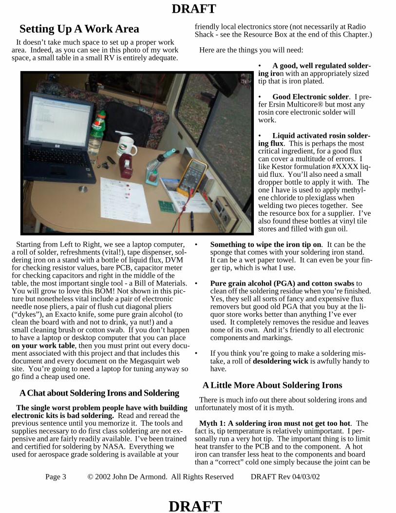
Setting Up A Work AreaIt doesn’t take much space to set up a proper work
area. Indeed, as you can see in this photo of my workspace, a small table in a small RV is entirely adequate.
Starting from Left to Right, we see a laptop computer,a roll of solder, refreshments (vital!), tape dispenser, sol-dering iron on a stand with a bottle of liquid flux, DVMfor checking resistor values, bare PCB, capacitor meterfor checking capacitors and right in the middle of thetable, the most important single tool - a Bill of Materials.You will grow to love this BOM! Not shown in this pic-ture but nonetheless vital include a pair of electronicneedle nose pliers, a pair of flush cut diagonal pliers(“dykes”), an Exacto knife, some pure grain alcohol (toclean the board with and not to drink, ya nut!) and asmall cleaning brush or cotton swab. If you don’t happento have a laptop or desktop computer that you can placeon your work table, then you must print out every docu-ment associated with this project and that includes thisdocument and every document on the Megasquirt website. You’re going to need a laptop for tuning anyway sogo find a cheap used one.
A Chat about Soldering Irons and Soldering
The single worst problem people have with buildingelectronic kits is bad soldering. Read and reread theprevious sentence until you memorize it. The tools andsupplies necessary to do first class soldering are not ex-pensive and are fairly readily available. I’ve been trainedand certified for soldering by NASA. Everything weused for aerospace grade soldering is available at your
friendly local electronics store (not necessarily at RadioShack - see the Resource Box at the end of this Chapter.)
Here are the things you will need:
• A good, well regulated solder-ing iron with an appropriately sizedtip that is iron plated.
• Good Electronic solder. I pre-fer Ersin Multicore® but most anyrosin core electronic solder willwork.
• Liquid activated rosin solder-ing flux. This is perhaps the mostcritical ingredient, for a good fluxcan cover a multitude of errors. Ilike Kestor formulation #XXXX liq-uid flux. You’ll also need a smalldropper bottle to apply it with. Theone I have is used to apply methyl-ene chloride to plexiglass whenwelding two pieces together. Seethe resource box for a supplier. I’vealso found these bottles at vinyl tilestores and filled with gun oil.
• Something to wipe the iron tip on. It can be thesponge that comes with your soldering iron stand.It can be a wet paper towel. It can even be your fin-ger tip, which is what I use.
• Pure grain alcohol (PGA) and cotton swabs toclean off the soldering residue when you’re finished.Yes, they sell all sorts of fancy and expensive fluxremovers but good old PGA that you buy at the li-quor store works better than anything I’ve everused. It completely removes the residue and leavesnone of its own. And it’s friendly to all electroniccomponents and markings.
• If you think you’re going to make a soldering mis-take, a roll of desoldering wick is awfully handy tohave.
A Little More About Soldering Irons
There is much info out there about soldering irons andunfortunately most of it is myth.
Myth 1: A soldering iron must not get too hot. Thefact is, tip temperature is relatively unimportant. I per-sonally run a very hot tip. The important thing is to limitheat transfer to the PCB and to the component. A hotiron can transfer less heat to the components and boardthan a “correct” cold one simply because the joint can be
Page 4 © 2002 John De Armond. All Rights Reserved DRAFT Rev 04/03/02
DRAFT
DRAFT
soldered so much faster. When the proper liquid flux isused, the solder practically jumps into the joint. If youlinger on a joint for more than a second, something iswrong with your technique.
Myth 2: A tiny tip is required . The fact is, most anysize tip you’re comfortable with will work. Generally asyour skills improve, you’ll want a larger tip. The larger
tip holds heat better so the soldering event is over withfaster. Less net heat to the component and board.
Myth 3: A soldering tip must be filed frequently tokeep it in shape. If you use an iron plated tip like I rec-ommend, it will need nothing other than cleaning and tin-ning over its useful life. Never, ever apply any sort ofabrasive to an iron plated tip! This includes files, SalAmoniac, sandpaper or scuffy pads. A light brushingwith a fine wire brush may be used if the tip gets cruftyfrom sitting hot for a longperiod of time. Anythingmore aggressive will removethe iron plating and then thetip becomes scrap metal.
Myth 4: <insert yourchemical or gadget here> isabsolutely vital for solder-ing. False. A lot of How-totexts were written before theiron plated tip came on themarket. Yes, with a purecopper tip, frequent filing isrequired (the copper slowlydissolves in the solder), as isdressing on a block of SalAmoniac. Just as we don’t
use vacuum tubes on our Megasquirt boards, neither dowe use this stuff on our irons.!
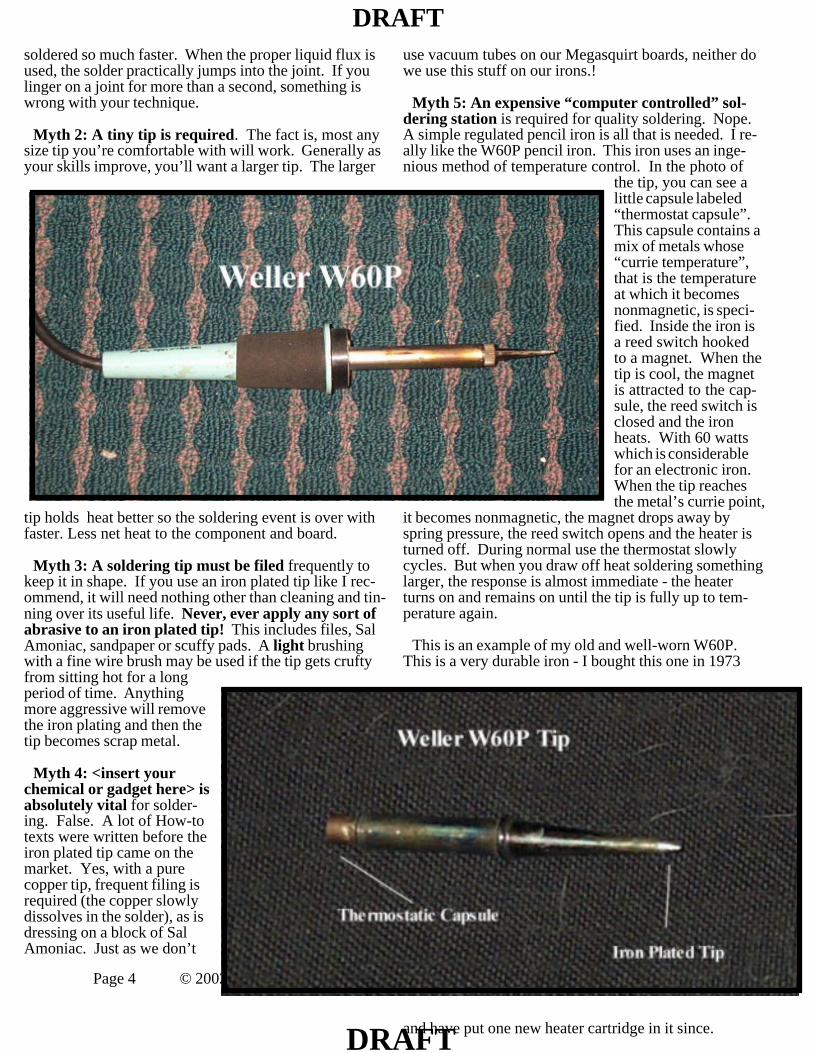
Myth 5: An expensive “computer controlled” sol-dering station is required for quality soldering. Nope.A simple regulated pencil iron is all that is needed. I re-ally like the W60P pencil iron. This iron uses an inge-nious method of temperature control. In the photo of
the tip, you can see alittle capsule labeled“thermostat capsule”.This capsule contains amix of metals whose“currie temperature”,that is the temperatureat which it becomesnonmagnetic, is speci-fied. Inside the iron isa reed switch hookedto a magnet. When thetip is cool, the magnetis attracted to the cap-sule, the reed switch isclosed and the ironheats. With 60 wattswhich is considerablefor an electronic iron.When the tip reachesthe metal’s currie point,
it becomes nonmagnetic, the magnet drops away byspring pressure, the reed switch opens and the heater isturned off. During normal use the thermostat slowlycycles. But when you draw off heat soldering somethinglarger, the response is almost immediate - the heaterturns on and remains on until the tip is fully up to tem-perature again.
This is an example of my old and well-worn W60P.This is a very durable iron - I bought this one in 1973
and have put one new heater cartridge in it since.
Page 5 © 2002 John De Armond. All Rights Reserved DRAFT Rev 04/03/02
DRAFT
DRAFT
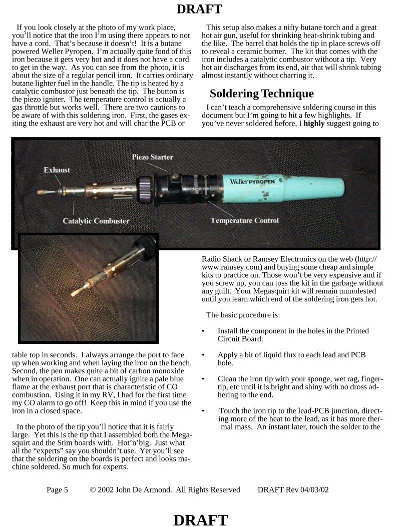
If you look closely at the photo of my work place,you’ll notice that the iron I’m using there appears to nothave a cord. That’s because it doesn’t! It is a butanepowered Weller Pyropen. I’m actually quite fond of thisiron because it gets very hot and it does not have a cordto get in the way. As you can see from the photo, it isabout the size of a regular pencil iron. It carries ordinarybutane lighter fuel in the handle. The tip is heated by acatalytic combustor just beneath the tip. The button isthe piezo igniter. The temperature control is actually agas throttle but works well. There are two cautions tobe aware of with this soldering iron. First, the gases ex-iting the exhaust are very hot and will char the PCB or
table top in seconds. I always arrange the port to faceup when working and when laying the iron on the bench.Second, the pen makes quite a bit of carbon monoxidewhen in operation. One can actually ignite a pale blueflame at the exhaust port that is characteristic of COcombustion. Using it in my RV, I had for the first timemy CO alarm to go off! Keep this in mind if you use theiron in a closed space.
In the photo of the tip you’ll notice that it is fairlylarge. Yet this is the tip that I assembled both the Mega-squirt and the Stim boards with. Hot’n’big. Just whatall the “experts” say you shouldn’t use. Yet you’ll seethat the soldering on the boards is perfect and looks ma-chine soldered. So much for experts.
This setup also makes a nifty butane torch and a greathot air gun, useful for shrinking heat-shrink tubing andthe like. The barrel that holds the tip in place screws offto reveal a ceramic burner. The kit that comes with theiron includes a catalytic combustor without a tip. Veryhot air discharges from its end, air that will shrink tubingalmost instantly without charring it.
Soldering TechniqueI can’t teach a comprehensive soldering course in this
document but I’m going to hit a few highlights. Ifyou’ve never soldered before, I highly suggest going to
Radio Shack or Ramsey Electronics on the web (http://www.ramsey.com) and buying some cheap and simplekits to practice on. Those won’t be very expensive and ifyou screw up, you can toss the kit in the garbage withoutany guilt. Your Megasquirt kit will remain unmolesteduntil you learn which end of the soldering iron gets hot.
The basic procedure is:
• Install the component in the holes in the PrintedCircuit Board.
• Apply a bit of liquid flux to each lead and PCBhole.
• Clean the iron tip with your sponge, wet rag, finger-tip, etc until it is bright and shiny with no dross ad-hering to the end.
• Touch the iron tip to the lead-PCB junction, direct-ing more of the heat to the lead, as it has more ther-mal mass. An instant later, touch the solder to the
Page 6 © 2002 John De Armond. All Rights Reserved DRAFT Rev 04/03/02
DRAFT
DRAFT
3-way junction of the iron, lead & PCB. The solderwill literally leap into the hole. Practically at the
same time, withdraw the iron and solder.
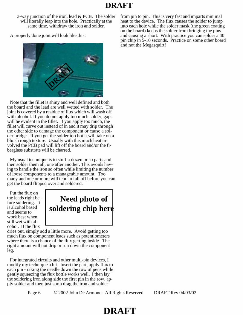
A properly done joint will look like this:
Note that the fillet is shiny and well defined and boththe board and the lead are well wetted with solder. Thejoint is covered by a residue of flux which will wash offwith alcohol. If you do not apply too much solder, gapswill be evident in the fillet. If you apply too much, thefillet will curve out instead of in and it may drip throughthe other side to damage the component or cause a sol-der bridge. If you get the solder too hot it will take on abluish rough texture. Usually with this much heat in-volved the PCB pad will lift off the board and/or the fi-berglass substrate will be charred.
My usual technique is to stuff a dozen or so parts andthen solder them all, one after another. This avoids hav-ing to handle the iron so often while limiting the numberof loose components to a manageable amount. Toomany and one or more will tend to fall off before you canget the board flipped over and soldered.
Put the flux onthe leads right be-fore soldering. Itis alcohol basedand seems towork best whenstill wet with al-cohol. If the fluxdries out, simply add a little more. Avoid getting toomuch flux on component leads such as potentiometerswhere there is a chance of the flux getting inside. Theright amount will not drip or run down the componentleg.
For integrated circuits and other multi-pin devices, Imodify my technique a bit. Insert the part, apply flux toeach pin - raking the needle down the row of pens whilegently squeezing the flux bottle works well. I then laythe soldering iron along side the first pin in the row, ap-ply solder and then just sorta drag the iron and solder
Need photo ofsoldering chip here
DRAFT
from pin to pin. This is very fast and imparts minimalheat to the device. The flux causes the solder to jumpinto each hole while the solder mask (the green coatingon the board) keeps the solder from bridging the pinsand causing a short. With practice you can solder a 40pin chip in 5-10 seconds. Practice on some other boardand not the Megasquirt!
Page 7 © 2002 John De Armond. All Rights Reserved DRAFT Rev 04/03/02
DRAFT
DRAFT
Component IdentificationBefore we leap crack open that nice blue box contain-
ing all the goodies, we have one more thing to cover.Component identification. Discussion on the Megasquirtmailing list indicate that many people are building a kitfor the first time so we’re going to take a bit about elec-tronic components. This is really basic but important.
In this kit we have a large variety of components in-cluding:
• resistors• capacitors• diodes• transistors• power FETs• Integrated circuits of various types• Mechanical components such as connectors, nuts,
bolts and the like.Within each category above there is a wide variety of
parts. Let’s look at some.
ResistorProbably the most basic component, it resists the flow
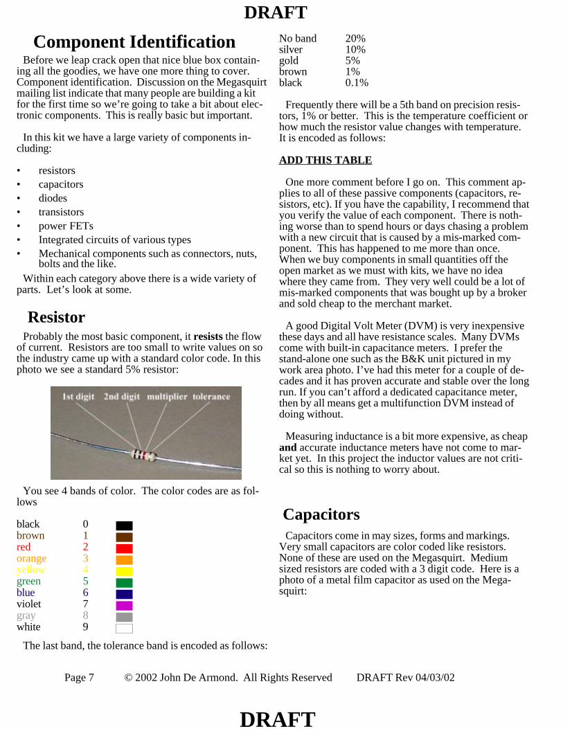
of current. Resistors are too small to write values on sothe industry came up with a standard color code. In thisphoto we see a standard 5% resistor:
You see 4 bands of color. The color codes are as fol-lows
black 0brown 1red 2orange 3yellow 4green 5blue 6violet 7gray 8white 9
The last band, the tolerance band is encoded as follows:
No band 20%silver 10%gold 5%brown 1%black 0.1%
Frequently there will be a 5th band on precision resis-tors, 1% or better. This is the temperature coefficient orhow much the resistor value changes with temperature.It is encoded as follows:
ADD THIS TABLE
One more comment before I go on. This comment ap-plies to all of these passive components (capacitors, re-sistors, etc). If you have the capability, I recommend thatyou verify the value of each component. There is noth-ing worse than to spend hours or days chasing a problemwith a new circuit that is caused by a mis-marked com-ponent. This has happened to me more than once.When we buy components in small quantities off theopen market as we must with kits, we have no ideawhere they came from. They very well could be a lot ofmis-marked components that was bought up by a brokerand sold cheap to the merchant market.
A good Digital Volt Meter (DVM) is very inexpensivethese days and all have resistance scales. Many DVMscome with built-in capacitance meters. I prefer thestand-alone one such as the B&K unit pictured in mywork area photo. I’ve had this meter for a couple of de-cades and it has proven accurate and stable over the longrun. If you can’t afford a dedicated capacitance meter,then by all means get a multifunction DVM instead ofdoing without.
Measuring inductance is a bit more expensive, as cheapand accurate inductance meters have not come to mar-ket yet. In this project the inductor values are not criti-cal so this is nothing to worry about.
CapacitorsCapacitors come in may sizes, forms and markings.
Very small capacitors are color coded like resistors.None of these are used on the Megasquirt. Mediumsized resistors are coded with a 3 digit code. Here is aphoto of a metal film capacitor as used on the Mega-squirt:
Page 8 © 2002 John De Armond. All Rights Reserved DRAFT Rev 04/03/02
DRAFT
DRAFT
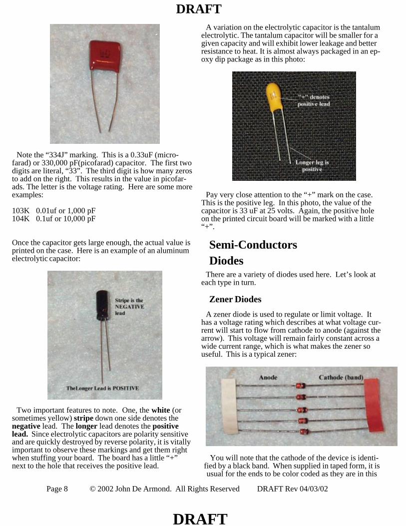
Note the “334J” marking. This is a 0.33uF (micro-farad) or 330,000 pF(picofarad) capacitor. The first twodigits are literal, “33”. The third digit is how many zerosto add on the right. This results in the value in picofar-ads. The letter is the voltage rating. Here are some moreexamples:
103K 0.01uf or 1,000 pF104K 0.1uf or 10,000 pF
Once the capacitor gets large enough, the actual value isprinted on the case. Here is an example of an aluminumelectrolytic capacitor:
Two important features to note. One, the white (orsometimes yellow) stripe down one side denotes thenegative lead. The longer lead denotes the positivelead. Since electrolytic capacitors are polarity sensitiveand are quickly destroyed by reverse polarity, it is vitallyimportant to observe these markings and get them rightwhen stuffing your board. The board has a little “+”next to the hole that receives the positive lead.
A variation on the electrolytic capacitor is the tantalumelectrolytic. The tantalum capacitor will be smaller for agiven capacity and will exhibit lower leakage and betterresistance to heat. It is almost always packaged in an ep-oxy dip package as in this photo:
Pay very close attention to the “+” mark on the case.This is the positive leg. In this photo, the value of thecapacitor is 33 uF at 25 volts. Again, the positive holeon the printed circuit board will be marked with a little“+”.
Semi-ConductorsDiodes
There are a variety of diodes used here. Let’s look ateach type in turn.
Zener Diodes
A zener diode is used to regulate or limit voltage. Ithas a voltage rating which describes at what voltage cur-rent will start to flow from cathode to anode (against thearrow). This voltage will remain fairly constant across awide current range, which is what makes the zener souseful. This is a typical zener:
You will note that the cathode of the device is identi-fied by a black band. When supplied in taped form, it isusual for the ends to be color coded as they are in this
Page 9 © 2002 John De Armond. All Rights Reserved DRAFT Rev 04/03/02
DRAFT
DRAFT
photo. The actual part number is printed on the glassbody, though it is usually difficult to read with the un-aided eye. This makes it doubly important to identify
and mark the diode per the BOM.
Epoxy Cased Diodes
Power and switching diodes are typically packaged inplastic epoxy cases. This photo is typical of the epoxydiodes used in this kit:
Again, note that the cathode end is identified by a bandprinted on the case. The actual part number is again
printed directly on the case, though like the glass diode,is frequently quite difficult to read.
TransistorsThere are two different types of transistors involved in
this project, bipolar junction transistors and powerMOS-FETs.
2N2222
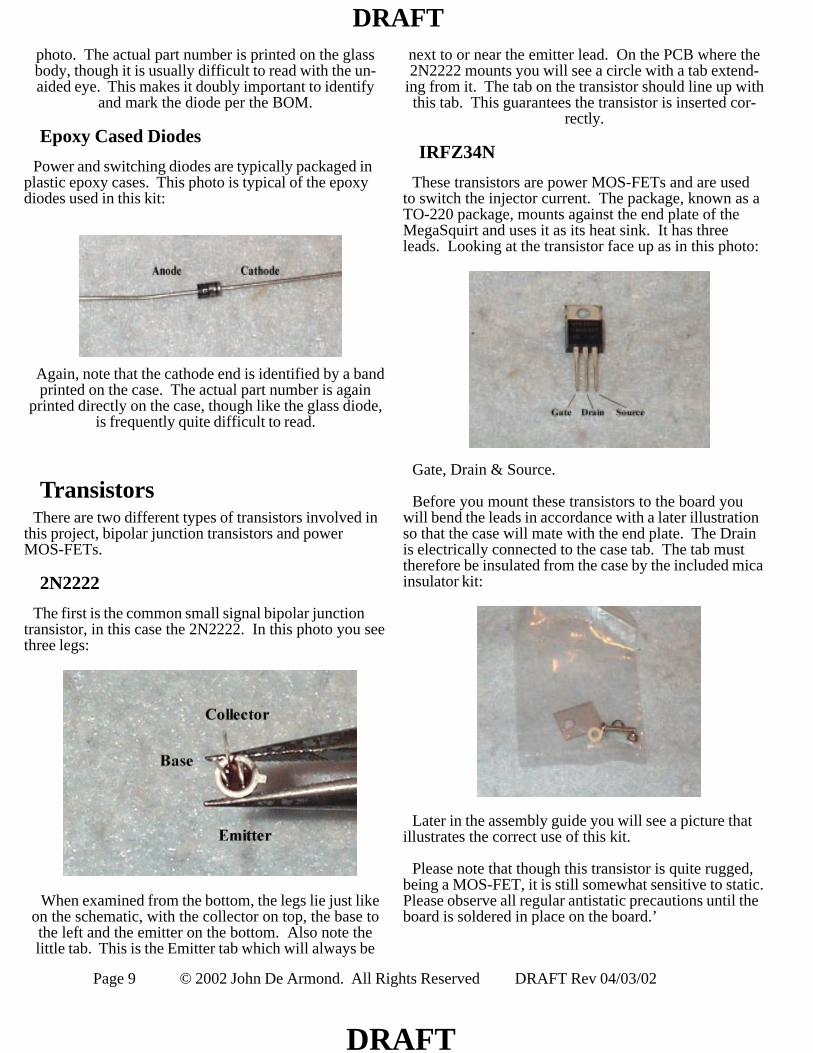
The first is the common small signal bipolar junctiontransistor, in this case the 2N2222. In this photo you seethree legs:
When examined from the bottom, the legs lie just likeon the schematic, with the collector on top, the base tothe left and the emitter on the bottom. Also note thelittle tab. This is the Emitter tab which will always be
next to or near the emitter lead. On the PCB where the2N2222 mounts you will see a circle with a tab extend-
ing from it. The tab on the transistor should line up withthis tab. This guarantees the transistor is inserted cor-
rectly.
IRFZ34N
These transistors are power MOS-FETs and are usedto switch the injector current. The package, known as aTO-220 package, mounts against the end plate of theMegaSquirt and uses it as its heat sink. It has threeleads. Looking at the transistor face up as in this photo:
Gate, Drain & Source.
Before you mount these transistors to the board youwill bend the leads in accordance with a later illustrationso that the case will mate with the end plate. The Drainis electrically connected to the case tab. The tab musttherefore be insulated from the case by the included micainsulator kit:
Later in the assembly guide you will see a picture thatillustrates the correct use of this kit.
Please note that though this transistor is quite rugged,being a MOS-FET, it is still somewhat sensitive to static.Please observe all regular antistatic precautions until theboard is soldered in place on the board.’
Page 10 © 2002 John De Armond. All Rights Reserved DRAFT Rev 04/03/02
DRAFT
DRAFT
Integrated CircuitsAll of the integrated circuits used in this project are
packaged in black epoxy dual in-line packages (DIPs)The part number is printed on the DIP.
4N25
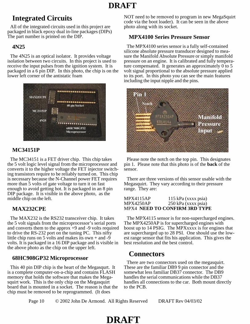
The 4N25 is an optical isolator. It provides voltageisolation between two circuits. In this project is used toreceive the input pulses from the ignition system. It ispackaged in a 6 pin DIP. In this photo, the chip is on thelower left corner of the antistatic foam
MC34151P
The MC34151 is a FET driver chip. This chip takesthe 5 volt logic level signal from the microprocessor andconverts it to the higher voltage the FET injector switch-ing transistors require to be reliably turned on. This chipis necessary because the N-Channel power FET requiresmore than 5 volts of gate voltage to turn it on fastenough to avoid getting hot. It is packaged in an 8 pinDIP package. It is visible in the above photo, as themiddle chip on the left.
MAX232CPE
The MAX232 is the RS232 transceiver chip. It takesthe 5 volt signals from the microprocessor’s serial portsand converts them to the approx +9 and -9 volts requiredto drive the RS-232 port on the tuning PC. This niftylittle chip runs on 5 volts and makes its own + and -9volts. It is packaged in a 16 DIP package and is visible inthe above photo as the chip on the upper left.
68HC908GP32 Microprocessor
This 40 pin DIP chip is the heart of the Megasqurt. Itis a complete computer-on-a-chip and contains FLASHmemory that holds the software that makes the Mega-squirt work. This is the only chip on the Megasquirtboard that is mounted in a socket. The reason is that thechip must be removed to be reprogrammed. (It does
NOT need to be removed to program in new MegaSquirtcode via the boot loader). It can be seen in the abovephoto along with its socket.
MPX4100 Series Pressure Sensor
The MPX4100 series sensor is a fully self-containedsilicone absolute pressure transducer designed to mea-sure the Manifold Absolute Pressure or simply manifoldpressure on an engine. It is calibrated and fully tempera-ture compensated. It generates an approximately 0 to 5volt signal proportional to the absolute pressure appliedto its port. In this photo you can see the main featuresincluding the input nipple and the pins.
Please note the notch on the top pin. This designatespin 1. Please note that this photo is of the back of thesensor.
There are three versions of this sensor usable with theMegasquirt. They vary according to their pressurerange. They are:
MPX4115AP 115 kPa (xxxx psia)MPX4250AP 250 kPa (xxxx psia)MPX4 NEED TO CONFIRM 3RD TYPE
The MPX4115 sensor is for non-supercharged engines.The MPX4250AP is for supercharged engines withboost up to 14 PSIG. The MPXxxxx is for engines thatare supercharged up to 28 PSI. One should use the low-est range sensor that fits his application. This gives thebest resolution and the best control.
ConnectorsThere are two connectors used on the megasquirt.
These are the familiar DB9 9 pin connector and thesomewhat less familiar DB37 connector. The DB9handles the serial communications while the DB37handles all connections to the car. Both mount directlyto the PCB.
Page 11 © 2002 John De Armond. All Rights Reserved DRAFT Rev 04/03/02
DRAFT
DRAFT
Receiving & InventoryingNow that we’ve learned what all the parts look like and
what tools to use, it’s time to think about opening thebox! You haven’t opened the box yet, have you?
The single most common problem kit buildershave is not properly receiving and inventoryingthe components.
Please read the above again and again and commit it tomemory. If you properly receive, inventory and sort yourkit components, you will almost never find any “missing”parts and you will find that the kit goes together easilyand with little confusion.
There are many successful methods of dealing with thathuge pile of tiny parts that confronts you when you doopen the box. I’ve worked out a method that has beensuccessful through dozens of projects and is easy to use.I present it here.
My method involves making a list of the components,normally from the Bill of Materials, that is in such a for-mat that you can physically tape each part next to its la-bel on the list. Normally you’d have to sit down andwrite or type out such a list but for the Megasquirtproject, I have saved you a lot of work. I have put thebill of materials in a spreadsheet (also a PDF file) thatyou can simply print out and use. The file is availablefrom several places (including this book). See the Re-source box for places on the Internet.
Inventorying Workplace
Before we open the box, we need to pick out a placeto do it. I highly recommend that it not be your normalworkbench. If your bench is like mine, it is clutteredwith tools and random components, has burn marks onthe bench from the soldering irons and probably sits on acluttered floor. This is the best place I know to findparts “missing”.
My favorite place is on a table with a neutral, or at leastfinely patterned surface on a solid color, preferably lightfloor. I normally use a table in my restaurant. For myfirst MegaSquirt kit, I used the neutral brown table in mymotor home. There should be nothing else on the tableother than the box of parts, the BOM sheets and a tapedispenser. And if your eyes are like mine, a strong mag-nifying glass! You, of course, need a good strong light,preferably overhead or over your shoulder to minimizethe shadows.
Opening the Box
OK, now that we have the bill of materials list, it’s timeto open the box. You did close the box back after youripped it open to see what was inside, right?
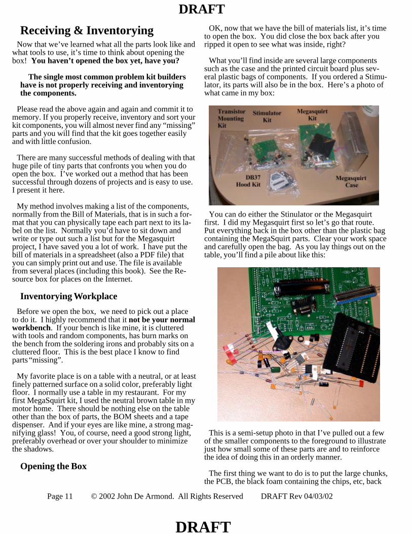
What you’ll find inside are several large componentssuch as the case and the printed circuit board plus sev-eral plastic bags of components. If you ordered a Stimu-lator, its parts will also be in the box. Here’s a photo ofwhat came in my box:
You can do either the Stinulator or the Megasquirtfirst. I did my Megasquirt first so let’s go that route.Put everything back in the box other than the plastic bagcontaining the MegaSquirt parts. Clear your work spaceand carefully open the bag. As you lay things out on thetable, you’ll find a pile about like this:
This is a semi-setup photo in that I’ve pulled out a fewof the smaller components to the foreground to illustratejust how small some of these parts are and to reinforcethe idea of doing this in an orderly manner.
The first thing we want to do is to put the large chunks,the PCB, the black foam containing the chips, etc, back
Page 12 © 2002 John De Armond. All Rights Reserved DRAFT Rev 04/03/02
DRAFT
DRAFT
in the baggie. We know what they are and we know thatwe received them so no need for them to clutter thingsup. The next thing is to divide the goodies into similarcomponents. The piles I use are
• Resistors
• Capacitors
• Transistors & similar devices
• Diodes
• Misc items such as the MAP transducer, chokes,etc.
Here’s a photo of the goodies after being sorted:
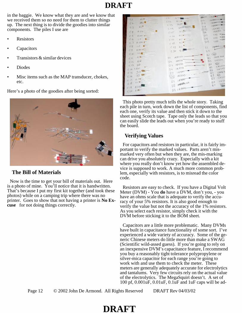
The Bill of Materials
Now is the time to get your bill of materials out. Hereis a photo of mine. You’ll notice that it is handwritten.That’s because I put my first kit together (and took thesephotos) while on a camping trip where there was noprinter. Goes to show that not having a printer is No Ex-cuse for not doing things correctly.
This photo pretty much tells the whole story. Takingeach pile in turn, work down the list of components, findeach one, verify its value and then stick it down to thesheet using Scotch tape. Tape only the leads so that youcan easily slide the leads out when you’re ready to stuffthe board.
Verifying Values
For capacitors and resistors in particular, it is fairly im-portant to verify the marked values. Parts aren’t mis-marked very often but when they are, the mis-markingcan drive you absolutely crazy. Especially with a kitwhere you really don’t know yet how the assembled de-vice is supposed to work. A much more common prob-lem, especially with resistors, is to misread the colorcode.
Resistors are easy to check. If you have a Digital VoltMeter (DVM) - You do have a DVM, don’t you, - youhave an ohms scale that is adequate to verify the accu-racy of your 5% resistors. It is also good enough toverify the value but not the accuracy of the 1% resistors.As you select each resistor, simply check it with theDVM before sticking it to the BOM sheet.
Capacitors are a little more problematic. Many DVMshave built in capacitance functionality of some sort. I’veexperienced a wide variety of accuracy. Some of the ge-neric Chinese meters do little more than make a SWAG(Scientific wild-assed guess). If you’re going to rely onan inexpensive DVM’s capacitance feature, I recommendyou buy a reasonably tight tolerance polypropylene orsilver-mica capacitor for each range you’re going towork with and use them to check the meter. Thesemeters are generally adequately accurate for electrolyticsand tantalums. Very few circuits rely on the actual valueof the electrolytics. The MegaSquirt doesn’t. A set of100 pf, 0.001uF, 0.01uF, 0.1uF and 1uF caps will be ad-

Page 13 © 2002 John De Armond. All Rights Reserved DRAFT Rev 04/03/02
DRAFT
DRAFT
equate for everything we’re dealing with here. Thesecaps can be had in 5% tolerance which is more than ad-equate for this application.
The best solution is a stand-alone capacitance meter.Here is the one I use:
<<<< PHOTO OF B&K METER >>>>
I’ve had this meter for 20+ years. I’m fairly sure B&Kstill sells a version. The up side is this meter and otherslike it is quite accurate. The down side is that it is some-what expensive. I think I paid about $100 for this meterand I doubt that they’ve gone down much. This meter iscommonly available used at Hamfests and otherswapmeets. A nice feature of an old piece of test equip-ment is that the component values have aged in and thedrift, if any, has stabilized to the very low long termvalue. Even though my meter is 20+ years old and haseven survived a shop fire (that’s why the face is stained),it remains dead-nuts on spec as verified with a GR stan-dard capacitor.
Let’s suppose that you don’t have a set of reference ca-pacitors and you’re not in a position to get them quickly.Say, you’re in a motor home on a camping trip! What todo? Well, we can play the statistics. We know (becausepeople have spent their lives studying this stuff) that ifwe sample a large number of capacitors of a given value,some will be spot-on, some will be greatly in error butmost will show errors that cluster around the nominalvalue. These errors lie on the normal or bell curve thatwe all learned about in statistics class (at least those ofus who didn’t sleep through that class!) Large errors arerelatively infrequent, lying far down on the skirts of thebell curve, so the odds of getting a component with alarge error are remote. On the other hand, if do get onewith an apparent large error, the odds are greatly in yourfavor that another in this lot will not be off that much.Since we have more than one of each of the various val-ues of capacitors in this kit, we can exploit this.
We will also exploit another characteristic. While yourgeneric chinese slave labor camp factory built(GCSLCFB) meter might not be very accurate, it prob-ably is very repeatable. That is, if you take a capacitorand plug it into the meter repeatedly, though the readingit produces each time might be greatly in error (poor ac-curacy), it will probably be the same wrong answer eachtime. We’re going to exploit this characteristic.
Let’s say we pick up one of the 0.1uF capacitors, plugit into our GCSLCFB meter and it reads 0.15uF. Takeit out and plug it back in a couple of times just to makesure it isn’t a bad contact. What to do? Grab anothercapacitor of the same or similar value and plug it in.Let’s say it reads 0.14uF. What does that tell us? It tells
us that the meter probably has a display error of 0.04uF.There is a remote possibility that both capacitors are inerror - there could be a systematic problem at the fac-tory, either in manufacturing, labeling or QC. But theodds are (remember the Bell curve) both capacitors arewithin tolerance. If you have a third capacitor and itagrees with the other two within a small tolerance, youcan greatly raise your confidence level.
What if the two or three capacitors don’t agree? Sup-pose one or two of them shows wild values? You simplydon’t know what you have! You’re going to have tofind a known standard, a calibrated entity, to resolve thedilemma. This can be either a calibrated capacitor or acalibrated instrument. This is the point where you si-lently thank Congress for funding the National Bureau ofStandards!
One of the handy things about this meter is the socketwhere you can simply push the leads of the componentinto the socket and read the value. Before checking eachcap, momentarily short the leads to remove any residualcharge that could damage the meter.
The LCR Bridge
A much better instrument if you are willing to part withthe money is the LCR (inductance, capacitance, resis-tance) bridge. While the DVM and dedicated capaci-tance meter can measure the capacitor’s value, it cannotmeasure its quality. The capacitor could read the rightcapacitance but be so leaky as to be worthless. TheDVM will not show that, at least not directly. The LCRbridge will. It measures not only the fundamental value,it also measures the quality. This quality is of variousparameters such as Q, dissipation factor, power factor,etc. All measure different forms of basically the samething - the quality of the component. It can measure thisquality of both capacitors and inductors (chokes). Ingeneral, you want a high Q, a low dissipation factor anda low power factor.
Here is a photo of my LCR bridge:
<<<<<< Photo of LCR bridge >>>>>>>>>>>>
This is a decent brand that I paid $175 used from a reli-able hamfest vendor whom I know. That’s a typicalprice. If you get really lucky and catch everyone snooz-ing on Ebay, you can get a digital LCR bridge for a fewhundred dollars instead of the several thousand they’reworth. Major brands are General Radio (GR), HewlettPackard, Tektronix and Fluke in that order. Both theanalog and the digital version of the GR bridges are ab-solutely top drawer quality instruments that are as rug-

Page 14 © 2002 John De Armond. All Rights Reserved DRAFT Rev 04/03/02
DRAFT
DRAFT
ged as a bridge and will retain their calibration for de-cades. Since it is unlikely that many people in my audi-ence have an LCR bridge, I’m not going to cover itsoperation here. All of them come with very good in-struction manuals that will walk you through the opera-tion.
There’s not anything on the MegaSquirt that demandsthe accuracy and precision of an LCR bridge so don’trun out and buy one just for this project. If you haveone, however, I recommend using it.
Workus Interruptus
Very few of us get to complete a task from beginningto end in one sitting. Especially those of us with wivesand girlfriends. The temptation is great to simply get upand walk away from work-in-progress to tend to theHoney-Doos. Funny how those resistors and capacitorsgrow legs and walk off when unattended. Just like a kid!The second great impulse is to sweep everything off in abox and stick it on a shelf. While Impulse #2 is definitelybetter than #1, it really isn’t the way to do it. Parts getstuck under the flaps of the box, boxes get yanked offthe shelf and spilled and so on. The beauty of my BOMmethod of accounting for parts is that you have an ideal,ready made solution to the workus interruptus problem.
Since all your small components are already stuckdown to sheets of paper, it follows that this paper can besafely filed away to protect the components. I use asmall 3-ring binder for the purpose. I simply punch theBOM sheets and put them in the binder. Put a couple ofblank pages on either side to protect them. Tape a labelon the binder so you know what it is and put it on theshelf for safekeeping. When you’re ready to go back towork, simply pop the book open and get going. You cansafely put the larger components such as the PCB, con-nectors and so on in a box but at least close the top,preferably running a hunk of tape across the top or else astrap.
At this point we have all of our small parts organized,inventoried and secured. If we’re missing any parts, nowis the time to obtain replacements. Once all parts are inhand, we whip out the soldering iron and get ready tounleash some blue smoke!
Page 15 © 2002 John De Armond. All Rights Reserved DRAFT Rev 04/03/02
DRAFT
DRAFT
Board FeaturesBefore we actually start burning solder, let’s take a
look at the printed circuit board (PCB). This may be oldhat for some of you but judging by the traffic on theMegaSquirt mailing list, there are a lot of folks whohave never seen a blank PCB.
This PCB was laid out using a software program calledOrCAD. OrCAD is a program specifically designed forPCB design. Once the design was complete, a series offiles (layout, drill tape, silk screen, etc) was output andsent off to a place that makes PCBs, commonly called aboard house or board foundry. The board housemakes films that contain the traces and are used to ex-pose a photosensitive coating on the blank PCB stock.The board is placed in a solution that eats away (etches)copper from wherever there isn’t a trace. Next, theboard is placed on a CNC drill and using the “drill tape”(because it used to be a paper tape) file, all holes aredrilled. Usually the next step is to tin-plate the tracesand then lay down a solder mask over all the board ex-cept where solder is supposed to stick. Then the holesare plated through with metal to make them conductive.The final step is usually to silk-screen on the silk-screenmask, the white ink with all the writing on it. Some-times, as in our case, where the board isn’t to be sol-dered immediately, it will be run through the wavesoldering machine to solder-plate the holes and vias.This can be seen as little smooth rounded ridges aroundthe holes.
The PCB has a component or silk screen side and asolder side. Quite obviously, the components go on thecomponent side (usually, but not always) and the solder-ing is done on the soldering side. If the MegaSquirt wasmanufactured commercially, the next step would involvestuffing the board with all the components using eitherhand labor or robots and then wave soldering every-thing at once. The wave soldering machine has a tank ofsolder and a pump that pumps the liquid solder over aweir so that a standing wave of liquid solder is estab-lished. A conveyer belt brings the stuffed board over theweir where the wave of solder contacts the board. Ev-erywhere there is not solder mask, solder adheres. Thewhole board is soldered in literally a couple of seconds.Our soldering will take a little longer!
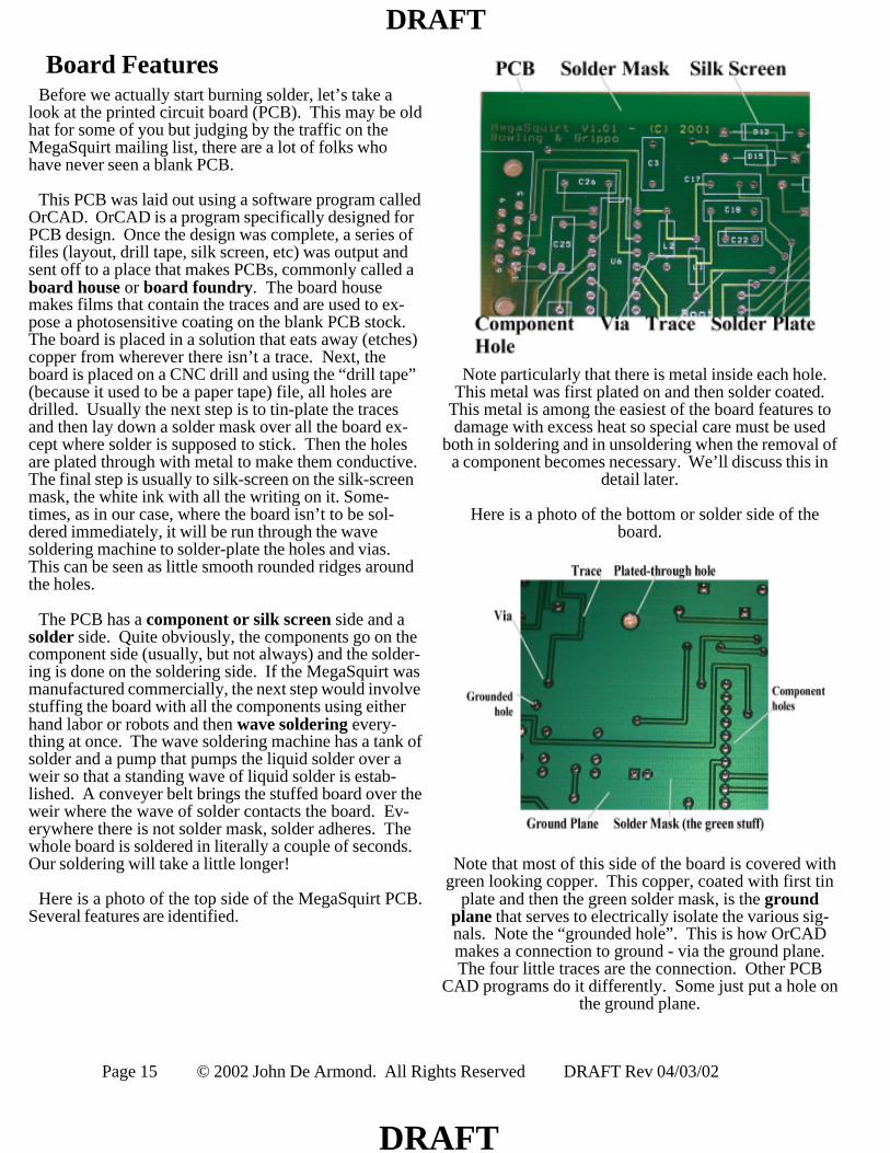
Here is a photo of the top side of the MegaSquirt PCB.Several features are identified.
Note particularly that there is metal inside each hole.This metal was first plated on and then solder coated.
This metal is among the easiest of the board features todamage with excess heat so special care must be used
both in soldering and in unsoldering when the removal ofa component becomes necessary. We’ll discuss this in
detail later.
Here is a photo of the bottom or solder side of theboard.
Note that most of this side of the board is covered withgreen looking copper. This copper, coated with first tin
plate and then the green solder mask, is the groundplane that serves to electrically isolate the various sig-nals. Note the “grounded hole”. This is how OrCADmakes a connection to ground - via the ground plane.The four little traces are the connection. Other PCB
CAD programs do it differently. Some just put a hole onthe ground plane.
Page 16 © 2002 John De Armond. All Rights Reserved DRAFT Rev 04/03/02
DRAFT
DRAFT
Note also that the solder mask (green stuff) goes all theway up to the edge of the solder plate on each hole.This mask serves to contain and control the solder,
makes hand soldering more convenient and makes ma-chine soldering possible.
An important characteristic of the solder mask is that itis an insulator. That means that if you have to probe a
trace during troubleshooting, you must either scrape thesolder mask away or exert enough force while wigglingthe probe, to penetrate to the copper trace. I don’t rec-ommend making a habit of probing traces because theyare very easy to break but sometimes it is necessary.
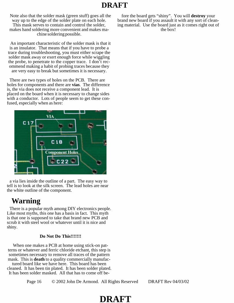
There are two types of holes on the PCB. There areholes for components and there are vias. The differenceis, the via does not receive a component lead. It isplaced on the board when it is necessary to change sideswith a conductor. Lots of people seem to get these con-fused, especially when as here:
a via lies inside the outline of a part. The easy way totell is to look at the silk screen. The lead holes are nearthe white outline of the component.
WarningThere is a popular myth among DIY electronics people.
Like most myths, this one has a basis in fact. This mythis that one is supposed to take that brand new PCB andscrub it with steel wool or whatever until it is nice andshiny.
Do Not Do This!!!!!!!
When one makes a PCB at home using stick-on pat-terns or whatever and ferric chloride etchant, this step issometimes necessary to remove all traces of the patternmask. This is death to a quality commercially manufac-
tured board like we have here. This board has beencleaned. It has been tin plated. It has been solder plated.It has been solder masked. All that has to come off be-
fore the board gets “shiny”. You will destroy yourbrand new board if you assault it with any sort of clean-ing material. Use the board just as it comes right out of
the box!

Page 17 © 2002 John De Armond. All Rights Reserved DRAFT Rev 04/03/02
DRAFT
DRAFT
Stuffing the BoardOK, we have our components sorted. We have our
workplace set up. We know about soldering irons andflux. We’re familiar with the bare PCB. Now is the timeto get down to the meat’n’potatoes of the project - turn-ing the PCB into a MegaSquirt. The first step is to stuffsome components.
Philosophy
There are several equally valid philosophies for stuffingthe board. One philosophy says to stuff all the big com-ponents first. Another says to stuff all the little onesfirst. Which one you choose depends a lot on the topol-ogy of the board. If you can see from the silk screen thatthere are lots of little components jammed up against thelarge ones, it is a good idea to stuff the large ones first.You can then go back and fit the small stuff around thelarge items. It becomes very difficult to bend, say, a re-lay around a bunch of interfering resistors or diodes! Onthe other hand, if a board is crowded and has a lot oflarge components, stuffing them first can make it difficultto get to the small part locations. To a great extent itbecomes a judgement call.
The MegaSquirt board is not crowded and there are nointerferences between large and small components. Mypreference, therefore, is to stuff the small stuff first.Small items generally require the assistance of needlenosed pliers. These can become difficult to maneuveraround the larger objects.
Assembly Sequence
When assembling the board, we want to proceed instages. We first want to get the power supply sectionworking so we can verify all the proper voltages beforewe put any semiconductors at risk. Once we know thepower is good, put the microprocessor in the socket andverify that it runs by scoping the clock pins. Once theprocessor is known to run, mount the MAX232 IC. TheMegaSquirt can then talk to the MegaTune program.Once communications with the PC and MegaTune pro-gram is verified, then stuff the rest of the semiconductorsexcept the power FETs and the MAP sensor. Fire up theMegaTune program, read the real time parameters andverify that the processor is reading something. If youhave your Stimulator board built, now is the time to con-nect it and verify that sensor data is being read. Alsoverify that the MegaSquirt LEDs flash. Finally, solder inthe FETs and the MAP sensor. Fire up the board on theStimulator and verify that the INJ LEDs on the stimula-tor flash. We’ll cover the checkout in detail later.
In particular, do the following:
• Stuff and solder the resistors, capacitors, small di-odes, the voltage regulator and LEDs• Stuff and solder the DB9 and DB37 connectors• Stuff and solder the 40 pin microprocessorsocket.• Power the board and verify that there is 5.0volts on pin 20 of the microprocessor socket.• Insert the microprocessor, power the board andverify that it works.• Stuff and solder the MAX232 chip. Hook upthe PC and verify that the processor talks to thePC.• Stuff and solder all other components exceptthe power FETs and the MAP sensor. Verifythat the board can read the Stimulator.• Stuff and solder the power FETs. Verify thatthe Stimulator INJ LEDs flash.• Stuff and solder the MAP sensor.
The board will then be finished and will be ready fordetailed checkout. This may not yet make completesense. But since you’re going to read this entire bookbefore firing up the soldering iron, that doesn’t matter.By the time you get to the end of this book, you will wellunderstand the above.
Technique
In general, you want to have the part in the net shapenecessary before inserting it into its holes. The reason isthat you want to avoid stressing the component near thebody. Many years ago when the earth was still hot and Iwas a nuclear engineer, a series of diode failures innuclear safety related equipment was traced to bendingthe leads too close to the body. The stress caused a par-tial debonding of the leads from the die which caused thelater failure of the part. It became the standard fornuclear-grade work to grip the part next to the bodywith needle-nosed pliers and bend the lead on the sideopposite the component. While we’re not building anuclear-safety-related device and don’t need to resort tothose measures, we do need to avoid unnecessary stress.In general, holding the part in your fingers and bendingthe leads with the other does not over stress the part.Tugging on the lead(s) to make the part lie flat after it isinserted does over stress the part.
How to Bend the Leads
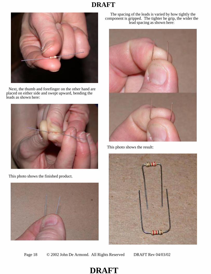
These photos show how to bend the leads. In thisphoto we see a resistor being held between the fingers.
Page 18 © 2002 John De Armond. All Rights Reserved DRAFT Rev 04/03/02
DRAFT
DRAFT
Next, the thumb and forefinger on the other hand areplaced on either side and swept upward, bending theleads as shown here:
This photo shows the finished product.
The spacing of the leads is varied by how tightly thecomponent is gripped. The tighter he grip, the wider the
lead spacing as shown here:
This photo shows the result:
Page 19 © 2002 John De Armond. All Rights Reserved DRAFT Rev 04/03/02
DRAFT
DRAFT
The proper spacing for resistors and diodes on thisboard will result from the loose grip where the bend
starts near the component package (Top component inthe previous photo.) This technique works for all axialleaded components. Most radial leaded (leads stick outof one end) components will already have the spacing
correct for the board pattern.
The Resistors
The first type of part I stuff is the resistor. There areseveral reasons. First, they’re easy to do and are cheap.Second, if you screw one up before you get in therhythm, it costs only pennies to replace. Third, there areusually more resistors than any other component. Unlessthere is a huge number of resistors, I stuff them all beforesoldering. Then I can zip rapidly through the solderingphase.
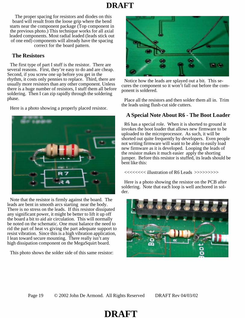
Here is a photo showing a properly placed resistor.
Note that the resistor is firmly against the board. Theleads are bent in smooth arcs starting near the body.There is no stress on the leads. If this resistor dissipatedany significant power, it might be better to lift it up offthe board a bit to aid air circulation. This will normallybe noted on the schematic. One must balance the need torid the part of heat vs giving the part adequate support toresist vibration. Since this is a high vibration application,I lean toward secure mounting. There really isn’t anyhigh dissipation component on the MegaSquirt board.
This photo shows the solder side of this same resistor:
Notice how the leads are splayed out a bit. This se-cures the component so it won’t fall out before the com-ponent is soldered.
Place all the resistors and then solder them all in. Trimthe leads using flush-cut side cutters.
A Special Note About R6 - The Boot Loader
R6 has a special role. When it is shorted to ground itinvokes the boot loader that allows new firmware to beuploaded to the microprocessor. As such, it will beshorted out quite frequently by developers. Even peoplenot writing firmware will want to be able to easily loadnew firmware as it is developed. Looping the leads ofthe resistor makes it much easier apply the shortingjumper. Before this resistor is stuffed, its leads should bebent like this:
<<<<<<<< illustration of R6 Leads >>>>>>>>>
Here is a photo showing the resistor on the PCB aftersoldering. Note that each loop is well anchored in sol-der.
Page 20 © 2002 John De Armond. All Rights Reserved DRAFT Rev 04/03/02
DRAFT
DRAFT
The Diodes
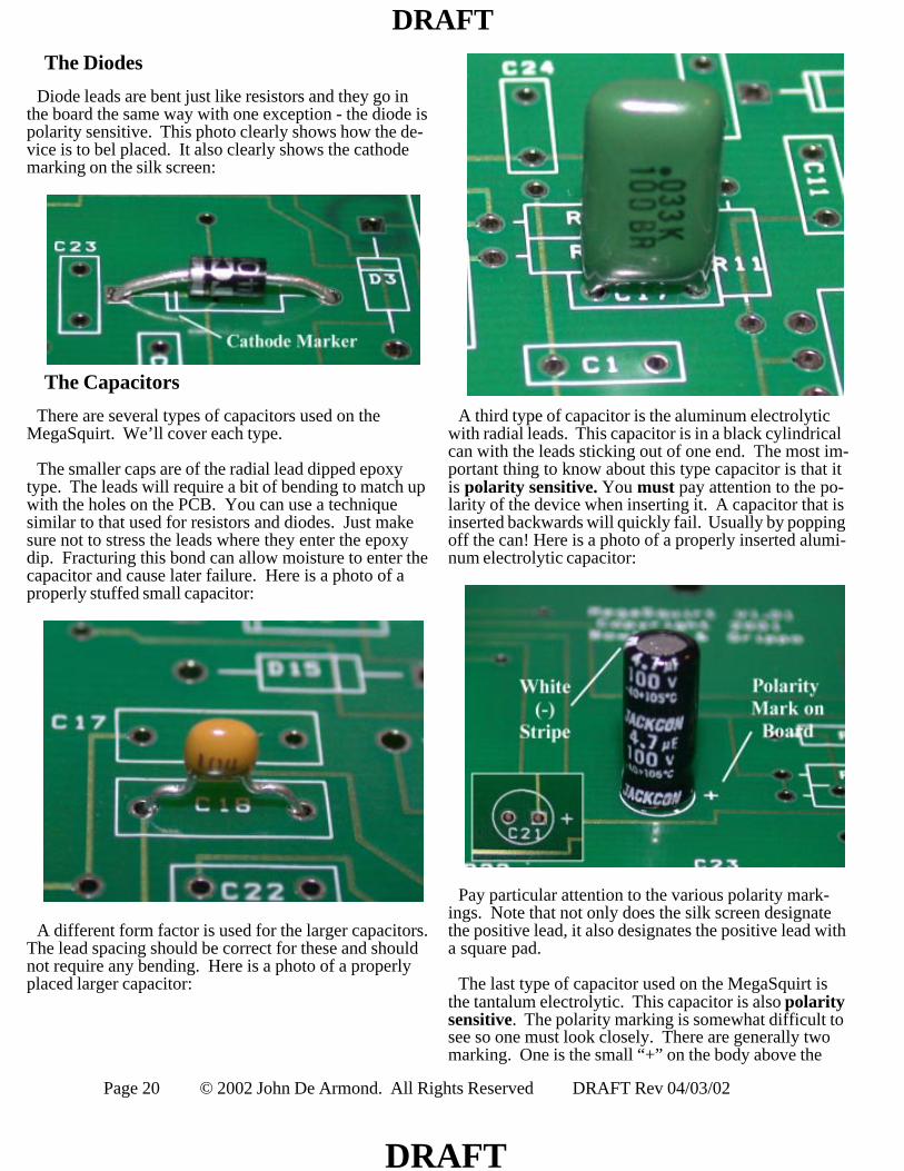
Diode leads are bent just like resistors and they go inthe board the same way with one exception - the diode ispolarity sensitive. This photo clearly shows how the de-vice is to bel placed. It also clearly shows the cathodemarking on the silk screen:
The Capacitors
There are several types of capacitors used on theMegaSquirt. We’ll cover each type.
The smaller caps are of the radial lead dipped epoxytype. The leads will require a bit of bending to match upwith the holes on the PCB. You can use a techniquesimilar to that used for resistors and diodes. Just makesure not to stress the leads where they enter the epoxydip. Fracturing this bond can allow moisture to enter thecapacitor and cause later failure. Here is a photo of aproperly stuffed small capacitor:
A different form factor is used for the larger capacitors.The lead spacing should be correct for these and shouldnot require any bending. Here is a photo of a properlyplaced larger capacitor:
A third type of capacitor is the aluminum electrolyticwith radial leads. This capacitor is in a black cylindricalcan with the leads sticking out of one end. The most im-portant thing to know about this type capacitor is that itis polarity sensitive. You must pay attention to the po-larity of the device when inserting it. A capacitor that isinserted backwards will quickly fail. Usually by poppingoff the can! Here is a photo of a properly inserted alumi-num electrolytic capacitor:
Pay particular attention to the various polarity mark-ings. Note that not only does the silk screen designatethe positive lead, it also designates the positive lead witha square pad.
The last type of capacitor used on the MegaSquirt isthe tantalum electrolytic. This capacitor is also polaritysensitive. The polarity marking is somewhat difficult tosee so one must look closely. There are generally twomarking. One is the small “+” on the body above the
Page 21 © 2002 John De Armond. All Rights Reserved DRAFT Rev 04/03/02
DRAFT
DRAFT
positive lead. The other is the positive lead is longer.Here is a photo of the tantalum device:
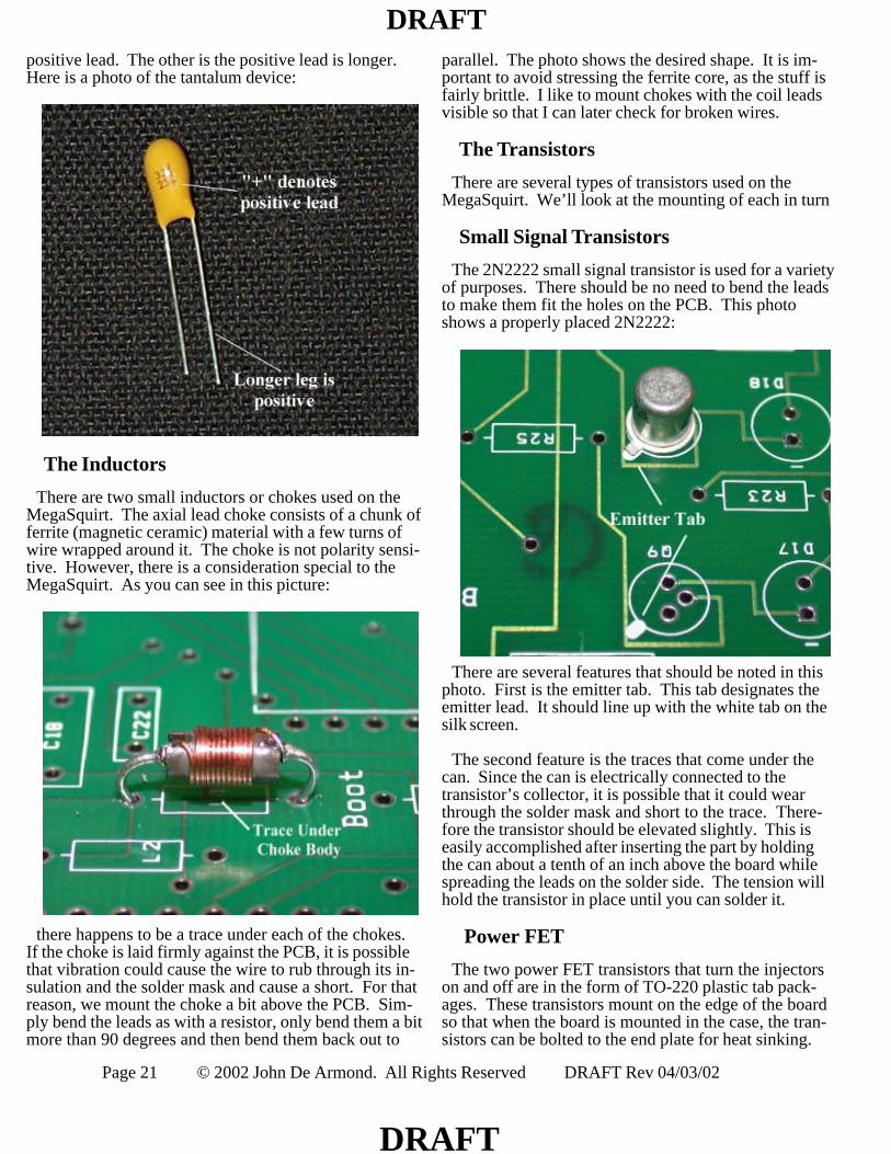
The Inductors
There are two small inductors or chokes used on theMegaSquirt. The axial lead choke consists of a chunk offerrite (magnetic ceramic) material with a few turns ofwire wrapped around it. The choke is not polarity sensi-tive. However, there is a consideration special to theMegaSquirt. As you can see in this picture:
there happens to be a trace under each of the chokes.If the choke is laid firmly against the PCB, it is possiblethat vibration could cause the wire to rub through its in-sulation and the solder mask and cause a short. For thatreason, we mount the choke a bit above the PCB. Sim-ply bend the leads as with a resistor, only bend them a bitmore than 90 degrees and then bend them back out to
parallel. The photo shows the desired shape. It is im-portant to avoid stressing the ferrite core, as the stuff isfairly brittle. I like to mount chokes with the coil leadsvisible so that I can later check for broken wires.
The Transistors
There are several types of transistors used on theMegaSquirt. We’ll look at the mounting of each in turn
Small Signal Transistors
The 2N2222 small signal transistor is used for a varietyof purposes. There should be no need to bend the leadsto make them fit the holes on the PCB. This photoshows a properly placed 2N2222:
There are several features that should be noted in thisphoto. First is the emitter tab. This tab designates theemitter lead. It should line up with the white tab on thesilk screen.
The second feature is the traces that come under thecan. Since the can is electrically connected to thetransistor’s collector, it is possible that it could wearthrough the solder mask and short to the trace. There-fore the transistor should be elevated slightly. This iseasily accomplished after inserting the part by holdingthe can about a tenth of an inch above the board whilespreading the leads on the solder side. The tension willhold the transistor in place until you can solder it.
Power FET
The two power FET transistors that turn the injectorson and off are in the form of TO-220 plastic tab pack-ages. These transistors mount on the edge of the boardso that when the board is mounted in the case, the tran-sistors can be bolted to the end plate for heat sinking.
Page 22 © 2002 John De Armond. All Rights Reserved DRAFT Rev 04/03/02
DRAFT
DRAFT
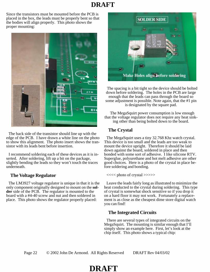
Since the transistors must be mounted before the PCB isplaced in the box, the leads must be properly bent so thatthe bodies will align properly. This photo shows theproper mounting:
The back side of the transistor should line up with theedge of the PCB. I have drawn a white line on the phototo show this alignment. The photo insert shows the tran-sistor with its leads bent before insertion.
I recommend soldering each of these devices as it is in-serted. After soldering, lift up a bit on the package,slightly bending the leads so they won’t touch the tracesunderneath.
The Voltage Regulator
The LM3927 voltage regulator is unique in that it is theonly component originally designed to mount on the sol-der side of the PCB. The regulator is mounted to theboard with a #4-40 screw and nut and then soldered inplace. This photo shows the regulator properly placed:
The spacing is a bit tight so the device should be bolteddown before soldering. The holes in the PCB are large
enough that the leads can pass through the board sosome adjustment is possible. Note again, that the #1 pin
is designated by the square pad.
The MegaSquirt power consumption is low enoughthat the voltage regulator does not require any heat sink-
ing other than being bolted down to the board.
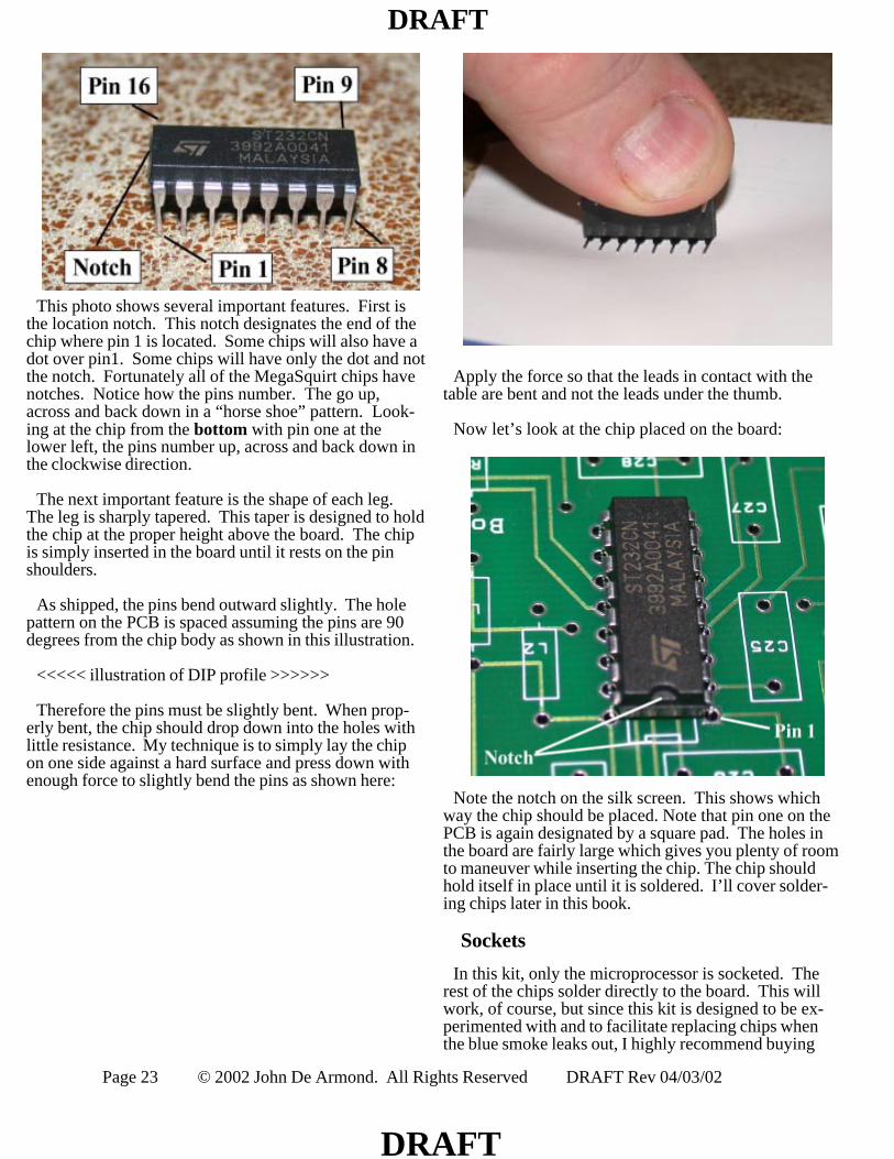
The Crystal
The MegaSquirt uses a tiny 32.768 Khz watch crystal.This device is too small and the leads are too weak tomount the device upright. Therefore it should be laiddown against the board, soldered in place and thenbonded with some sort of adhesive. I like silicone RTV.Superglue, polyurethane and hot melt adhesive are othergood choices. Here is a photo of the crystal in place be-fore soldering and bonding.
<<<< photo of crystal >>>>>
Leave the leads fairly long as illustrated to minimize theheat conducted to the crystal during soldering. This typeof crystal is somewhat shock sensitive so if you drop iton a hard floor it may not work. Fortunately a replace-ment is as close as the cheapest dime store digital watchyou can find!
The Integrated Circuits
There are several types of integrated circuits on theMegaSquirt. The mounting is similar enough that I’llsimply show an example here. First, let’s look at thechip itself. This photo shows a typical chip:
Page 23 © 2002 John De Armond. All Rights Reserved DRAFT Rev 04/03/02
DRAFT
DRAFT
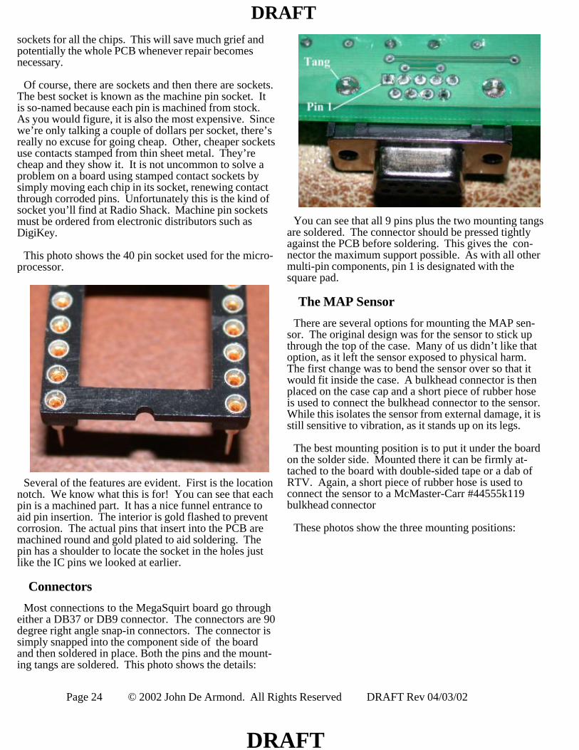
This photo shows several important features. First isthe location notch. This notch designates the end of thechip where pin 1 is located. Some chips will also have adot over pin1. Some chips will have only the dot and notthe notch. Fortunately all of the MegaSquirt chips havenotches. Notice how the pins number. The go up,across and back down in a “horse shoe” pattern. Look-ing at the chip from the bottom with pin one at thelower left, the pins number up, across and back down inthe clockwise direction.
The next important feature is the shape of each leg.The leg is sharply tapered. This taper is designed to holdthe chip at the proper height above the board. The chipis simply inserted in the board until it rests on the pinshoulders.
As shipped, the pins bend outward slightly. The holepattern on the PCB is spaced assuming the pins are 90degrees from the chip body as shown in this illustration.
<<<<< illustration of DIP profile >>>>>>
Therefore the pins must be slightly bent. When prop-erly bent, the chip should drop down into the holes withlittle resistance. My technique is to simply lay the chipon one side against a hard surface and press down withenough force to slightly bend the pins as shown here:
Apply the force so that the leads in contact with thetable are bent and not the leads under the thumb.
Now let’s look at the chip placed on the board:
Note the notch on the silk screen. This shows whichway the chip should be placed. Note that pin one on thePCB is again designated by a square pad. The holes inthe board are fairly large which gives you plenty of roomto maneuver while inserting the chip. The chip shouldhold itself in place until it is soldered. I’ll cover solder-ing chips later in this book.
Sockets
In this kit, only the microprocessor is socketed. Therest of the chips solder directly to the board. This willwork, of course, but since this kit is designed to be ex-perimented with and to facilitate replacing chips whenthe blue smoke leaks out, I highly recommend buying
Page 24 © 2002 John De Armond. All Rights Reserved DRAFT Rev 04/03/02
DRAFT
DRAFT
sockets for all the chips. This will save much grief andpotentially the whole PCB whenever repair becomesnecessary.
Of course, there are sockets and then there are sockets.The best socket is known as the machine pin socket. Itis so-named because each pin is machined from stock.As you would figure, it is also the most expensive. Sincewe’re only talking a couple of dollars per socket, there’sreally no excuse for going cheap. Other, cheaper socketsuse contacts stamped from thin sheet metal. They’recheap and they show it. It is not uncommon to solve aproblem on a board using stamped contact sockets bysimply moving each chip in its socket, renewing contactthrough corroded pins. Unfortunately this is the kind ofsocket you’ll find at Radio Shack. Machine pin socketsmust be ordered from electronic distributors such asDigiKey.
This photo shows the 40 pin socket used for the micro-processor.
Several of the features are evident. First is the locationnotch. We know what this is for! You can see that eachpin is a machined part. It has a nice funnel entrance toaid pin insertion. The interior is gold flashed to preventcorrosion. The actual pins that insert into the PCB aremachined round and gold plated to aid soldering. Thepin has a shoulder to locate the socket in the holes justlike the IC pins we looked at earlier.
Connectors
Most connections to the MegaSquirt board go througheither a DB37 or DB9 connector. The connectors are 90degree right angle snap-in connectors. The connector issimply snapped into the component side of the boardand then soldered in place. Both the pins and the mount-ing tangs are soldered. This photo shows the details:
You can see that all 9 pins plus the two mounting tangsare soldered. The connector should be pressed tightlyagainst the PCB before soldering. This gives the con-nector the maximum support possible. As with all othermulti-pin components, pin 1 is designated with thesquare pad.
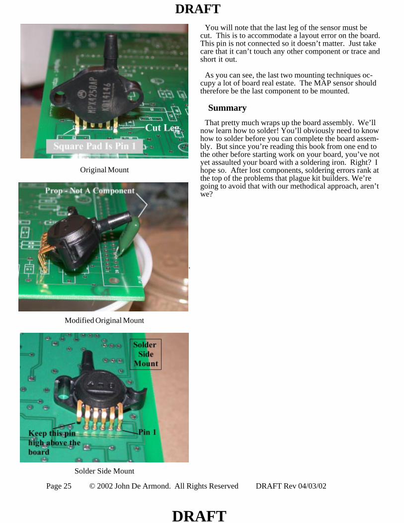
The MAP Sensor
There are several options for mounting the MAP sen-sor. The original design was for the sensor to stick upthrough the top of the case. Many of us didn’t like thatoption, as it left the sensor exposed to physical harm.The first change was to bend the sensor over so that itwould fit inside the case. A bulkhead connector is thenplaced on the case cap and a short piece of rubber hoseis used to connect the bulkhead connector to the sensor.While this isolates the sensor from external damage, it isstill sensitive to vibration, as it stands up on its legs.
The best mounting position is to put it under the boardon the solder side. Mounted there it can be firmly at-tached to the board with double-sided tape or a dab ofRTV. Again, a short piece of rubber hose is used toconnect the sensor to a McMaster-Carr #44555k119bulkhead connector
These photos show the three mounting positions:
Page 25 © 2002 John De Armond. All Rights Reserved DRAFT Rev 04/03/02
DRAFT
DRAFT
Original Mount
.
Modified Original Mount
Solder Side Mount
You will note that the last leg of the sensor must becut. This is to accommodate a layout error on the board.This pin is not connected so it doesn’t matter. Just takecare that it can’t touch any other component or trace andshort it out.
As you can see, the last two mounting techniques oc-cupy a lot of board real estate. The MAP sensor shouldtherefore be the last component to be mounted.
Summary
That pretty much wraps up the board assembly. We’llnow learn how to solder! You’ll obviously need to knowhow to solder before you can complete the board assem-bly. But since you’re reading this book from one end tothe other before starting work on your board, you’ve notyet assaulted your board with a soldering iron. Right? Ihope so. After lost components, soldering errors rank atthe top of the problems that plague kit builders. We’regoing to avoid that with our methodical approach, aren’twe?


![Netop Pack'n Deploy User's Guide - SystemSoftware.at€¦ · 1 Netop Pack'n Deploy Netop Pack'n Deploy User's Guide 31 January 2017 3 Folder: []: Will show the destination directory](https://img.pdfslide.net/doc/110x75/6013ebb2d8d272188838bc8f/netop-packn-deploy-users-guide-1-netop-packn-deploy-netop-packn-deploy-users.jpg)