Embed Size (px)
Citation preview

Mehdi Alimadadi, Samad Sheikhaei,
Guy Lemieux, Shahriar Mirabbasi, Patrick Palmer
University of British Columbia (UBC)
Vancouver, BC, Canada
A 3GHz Switching DC-DC ConverterUsing Clock-Tree Charge-Recycling
in 90nm CMOS with Integrated Output Filter

2
Motivation
• Power-limited CPU performance
– Trend: > 4 CPU cores on one chip
• Solution?
– Dynamic Voltage and Frequency Scaling (DVFS)
- Each core scaled differently based on load
– Need multiple supply voltages on-chip
2VfCP

3
Motivation
• How to supply multiple voltages?
Our approach …– Global voltage distribution (high Vdd)– Local voltage regulation (on-chip, low Vdd)
Support for … – Coarse-grain voltage islands (e.g., CPU cores)– Fine-grain voltage islands (e.g., ALU, FPU, …)
On-chip “local” voltage regulation

4
Problem Definition
• On-chip “local” voltage regulation
• Constraints– On-chip components, “standard” CMOS– Scaled down voltage buck converters
• Shrink L, C to fit on-chip
– Efficiency trade-off• Local regulator consumes power• Local regulator saves power by DVFS
consumption < savings

5
Summary Results
• On-chip DC-DC buck (step-down) converter– Standard 90nm CMOS– 1V input, 0.5~0.7V output, 100mA– Up to 158% effective efficiency
• Over 100% !!!???– By recycling charge thrown away in clock tree
• High-speed operation– 3GHz CPU clock 3GHz buck converter
• Monolithic L and C (converter area 0.27mm2)– Unique ZVS delay circuit improves efficiency

6
Switch Mode Power Supply
• CMOS inverter as power switches in buck converter
C R
Vgate VoutVinv
Vdd
S
D
IL
LL
R
VoutVinv
DS
-+Vin C
Vgate
IL

7
Clock and SMPS Merging
• CPU clock: 3GHz clock and large Cclk
• SMPS: large Mp, Mn drive chain

8
Clock and SMPS Merging
• Combine the driver circuits
Vclk
Cclk
CLK in
Mp
Mn
VoutLf
Cf Rload
CLK in

9
Key Contribution: CHARGE RECYCLING
• Benefits– Shared driver chain
– Cclk added to SMPS
• Note: NMOS drains Cclk, wastes charge!
• Delaying NMOS ZVS recycles clock charge!
Vclk
Cclk
CLK in
VoutLf
Cf Rload
10
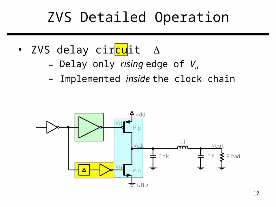
ZVS Detailed Operation
• ZVS delay circuit – Delay only rising edge of Vn
– Implemented inside the clock chain
Mp
Mn
GND
Vdd
Vn
Vp
VoutVclkLf
Cclk Cf Rload
11
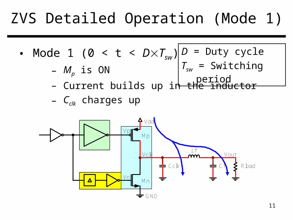
ZVS Detailed Operation (Mode 1)
• Mode 1 (0 < t < DTsw)
– Mp is ON
– Current builds up in the inductor
– Cclk charges up
Mp
Mn
GND
Vdd
Vn
Vp
VoutVclkLf
Cclk Cf Rload
D = Duty cycle
Tsw = Switching period
12
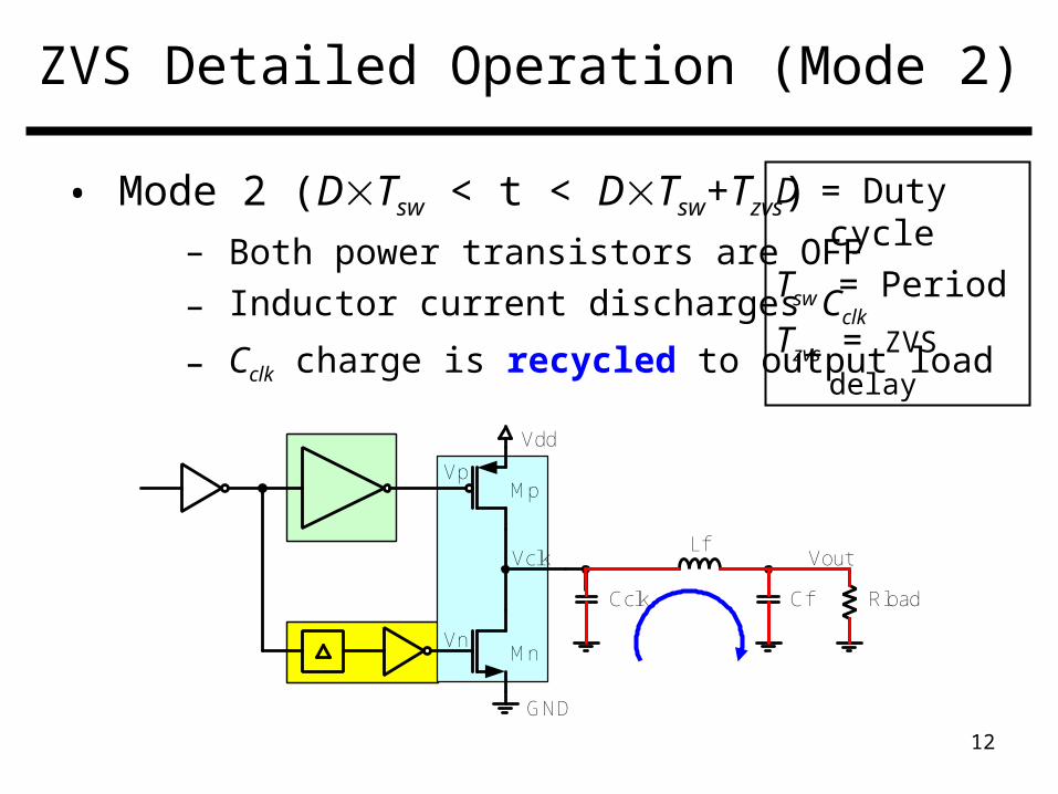
ZVS Detailed Operation (Mode 2)
• Mode 2 (DTsw < t < DTsw+Tzvs)– Both power transistors are OFF
– Inductor current discharges Cclk
– Cclk charge is recycled to output load
Mp
Mn
GND
Vdd
Vn
Vp
VoutVclkLf
Cclk Cf Rload
D = Duty cycle
Tsw = Period
Tzvs = ZVS delay

13
ZVS Detailed Operation (Mode 3)
• Mode 3 (DTsw+Tzvs < t < Tsw)
– Mn turns ON when Vclk 0
• ZVS for Mn
– Inductor current decreases linearly
Mp
Mn
GND
Vdd
Vn
Vp
VoutVclkLf
Cclk Cf Rload
D = Duty cycle
Tsw = Period
Tzvs = ZVS delay

14
Detailed Operation
• ZVS delay circuit for Mn
– Delay rising edge of Vn
Mp
Mn
GND
Vdd
Vm
Vn
Vp
Vclk
M3
M4
M1
M2
ZVS Delay Circuit
12
3
4
Vout
RloadCclk
Lf
Cf

15
Detailed Operation
• Adaptive ZVS delay circuit for Mn
– Falling edges of Vp and Vn are synchronized
Mp
Mn
GND
Vdd
Vm
Vn
Vp
Vclk
M3
M4
M1
M2
ZVS Delay Circuit
12
2
Vout
RloadCclk
Lf
Cf
16
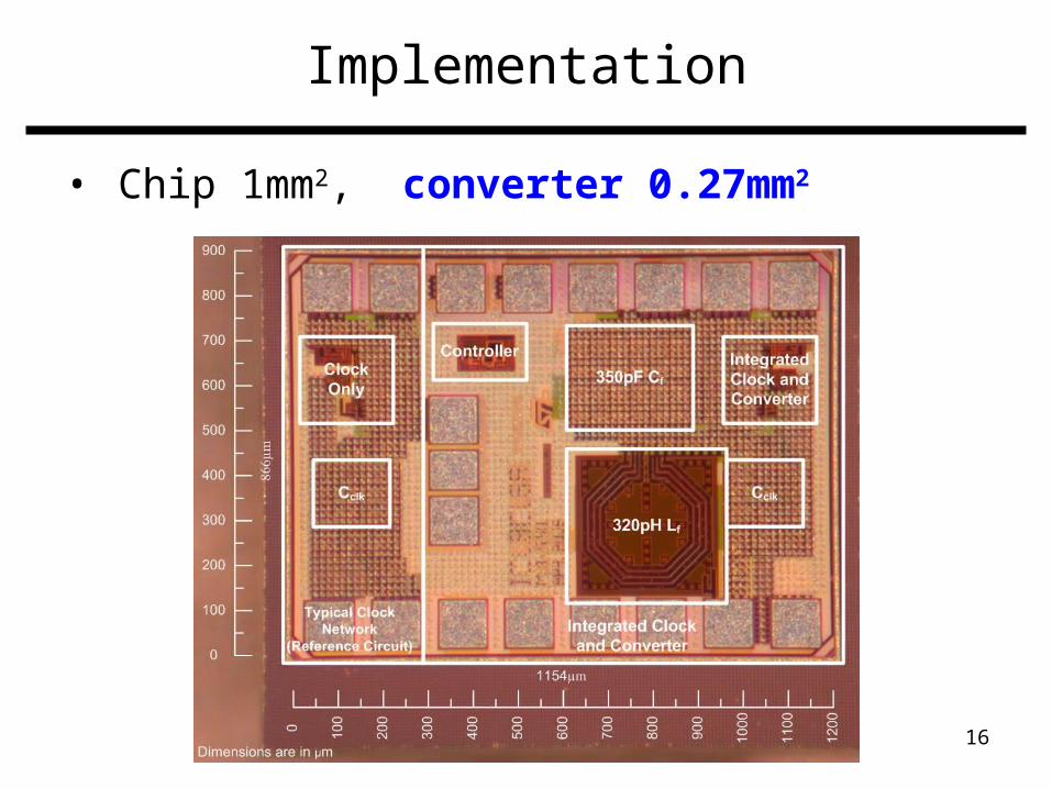
Implementation
• Chip 1mm2, converter 0.27mm2

17
Implementation
• Charge recycling of the clock tree capacitor
Reference clock circuit
Circuit 2, Pin2
Combined SMPS
+ clock circuit
Circuit 1, Pin1, Pout1
Rload
Cclk
CLK in
VoutLf
CfCclk
CLK in Vclk
18
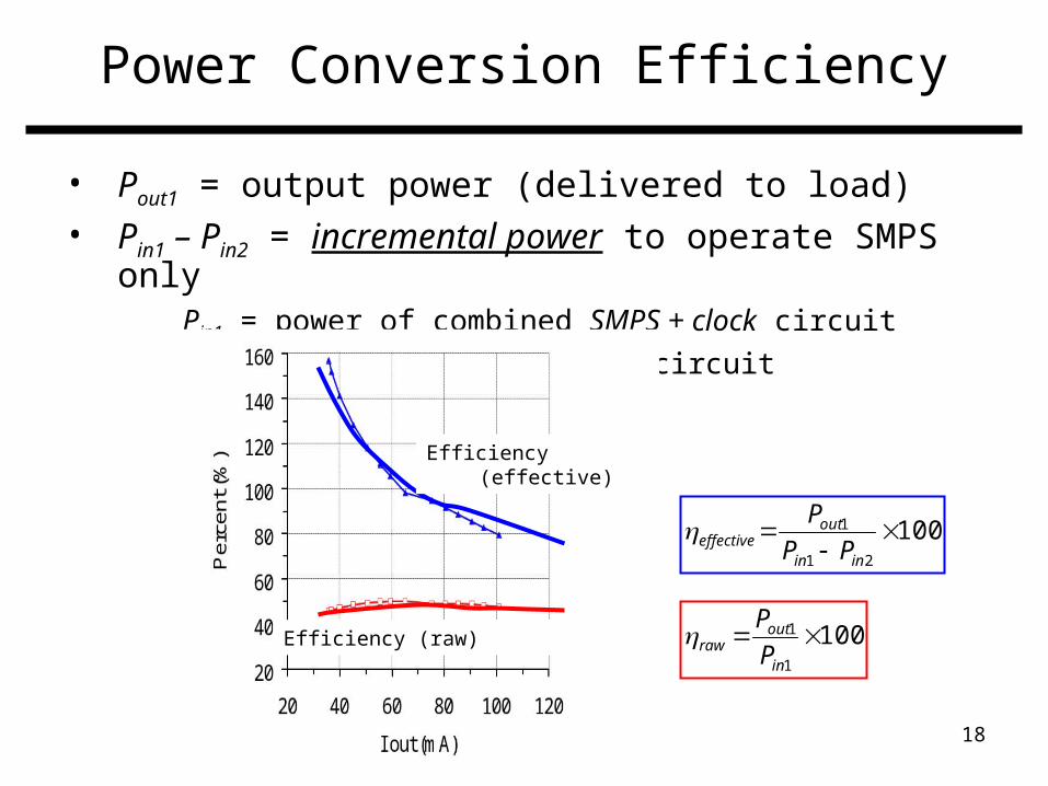
Power Conversion Efficiency
• Pout1 = output power (delivered to load)• Pin1 – Pin2 = incremental power to operate SMPS only
Pin1 = power of combined SMPS + clock circuit
Pin2 = power of reference clock circuit
10021
1
inin
outeffective PP
P
1001
1 in
outraw P
PEfficiency (raw)
Efficiency (effective)
19
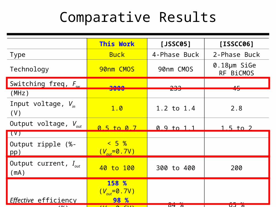
Comparative Results
This Work [JSSC05] [ISSCC06]
Type Buck 4-Phase Buck 2-Phase Buck
Technology 90nm CMOS 90nm CMOS0.18µm SiGe RF BiCMOS
Switching freq, Fsw (MHz) 3000 233 45
Input voltage, Vin (V) 1.0 1.2 to 1.4 2.8
Output voltage, Vout (V) 0.5 to 0.7 0.9 to 1.1 1.5 to 2
Output ripple (%-pp) < 5 % (Vout=0.7V)
Output current, Iout (mA) 40 to 100 300 to 400 200
Effective efficiency eff (%)
158 % (Vout=0.7V)
98 % (Vout=0.6V)
80 % (Vout=0.5V)84 % 65 %
Filter inductor, Lf (nH) 0.32 6.8 (per phase) 11 (per phase)
Filter capacitor, Cf (pF) 350 2500 6000
Off/on chip Lf, Cf On-chip Off-chip L On-chip
Converter area (mm2) 0.27 0.14 (excl. L & C) 27

20
Contributions
• Key concepts– High switching frequency saves area– Combined drivers saves area and switching loss
– Recycled charge converter load discharges Cclk
– Unique ZVS delay circuit lower power loss
• Limitations– Regulation needs variable duty cycle clock
• May introduce additional clock jitter• Mostly suitable for edge-triggered blocks
(no latches)

21
References
[JSSC05] P. Hazucha, G. Schrom, H. Jaehong, B. A. Bloechel, P. Hack, G. E. Dermer, S. Narendra, D. Gardner, T. Karnik, V. De, and S. Borkar, “A 233MHz 80%-87% Efficient Four-Phase DC-DC Converter Utilizing Air-Core Inductors on Package,” IEEE J. Solid-State Circuits, vol. 40, pp. 838-845, Apr., 2005.
[ISSCC06] S. Abedinpour, B. Bakkaloglu, and S. Kiaei, “A Multi-Stage Interleaved Synchronous Buck Converter with Integrated Output Filter in a 0.18µm SiGe Process,” ISSCC Dig. Tech. Papers, pp. 356-357, Feb., 2006.