Embed Size (px)
Citation preview
Portland State University Portland State University
PDXScholar PDXScholar
Electrical and Computer Engineering Faculty Publications and Presentations Electrical and Computer Engineering
4-2017
Memcapacitive Devices in Logic and Crossbar Memcapacitive Devices in Logic and Crossbar
Applications Applications
Dat Tran Portland State University, [email protected]
Christof Teuscher Portland State University, [email protected]
Follow this and additional works at: https://pdxscholar.library.pdx.edu/ece_fac
Part of the Computer Engineering Commons
Let us know how access to this document benefits you.
Citation Details Citation Details Tran, Dat and Teuscher, Christof, "Memcapacitive Devices in Logic and Crossbar Applications" (2017). Electrical and Computer Engineering Faculty Publications and Presentations. 417. https://pdxscholar.library.pdx.edu/ece_fac/417
This Pre-Print is brought to you for free and open access. It has been accepted for inclusion in Electrical and Computer Engineering Faculty Publications and Presentations by an authorized administrator of PDXScholar. Please contact us if we can make this document more accessible: [email protected].
arX
iv:1
704.
0592
1v1
[cs
.ET
] 1
9 A
pr 2
017
Memcapacitive Devices in Logic and Crossbar
Applications
DAT TRAN, S. J.⋆, CHRISTOF TEUSCHER
Department of Electrical and Computer Engineering
Portland State University, Portland, OR, USA
Received 25 December 2016; In final form 1 April 2017
Over the last decade, memristive devices have been widely ad-
opted in computing for various conventional and unconventional
applications. While the integration density, memory property,
and nonlinear characteristics have many benefits, reducing the
energy consumption is limited by the resistive nature of the de-
vices. Memcapacitors would address that limitation while still
having all the benefits of memristors. Recent work has shown
that with adjusted parameters during the fabrication process, a
metal-oxide device can indeed exhibit a memcapacitive behav-
ior. We introduce novel memcapacitive logic gates and memca-
pacitive crossbar classifiers as a proof of concept that such ap-
plications can outperform memristor-based architectures. The
results illustrate that, compared to memristive logic gates, our
memcapacitive gates consume about 7× less power. The mem-
capacitive crossbar classifier achieves similar classification per-
formance but reduces the power consumption by a factor of about
1, 500× for the MNIST dataset and a factor of about 1, 000× for
the CIFAR-10 dataset compared to a memristive crossbar. Our
simulation results demonstrate that memcapacitive devices have
great potential for both Boolean logic and analog low-power ap-
plications.
Key words: memcapacitor, memristor, logic, crossbar, classifier
⋆ email: [email protected]
1
1 INTRODUCTION
The ever-growing demand for more speed and lower power in circuit design
poses significant challenges for the continuing scaling of today’s CMOS tech-
nology. Fundamental physical as well as architectural limits lead to new bot-
tlenecks. While the advent of multicore architectures alleviated some of the
challenges, more cores do not always mean better: only a fraction of the
cores typically operate at full speed because of Amdal’s law and power con-
straints [12]. Finding alternative devices and architectures beyond CMOS,
beyond Boolean logic, and beyond von Neumann architectures has been a
major driver of the unconventional computing community.
Memristive devices [44] have been widely adopted in previous years for
various conventional and unconventional applications. They have shown great
promise for high integration densities as well as low energy consumption
[17, 38, 41], for example for neuromorphic applications [15, 22, 23, 46, 58]
and for memristor-based logic circuit design [49]. However, the energy con-
sumption of memristors is bounded by the resistive nature of these devices.
That is where memcapacitors [4, 29], another mem-element, may have further
benefits.
Recent work demonstrated a memcapacitive response in a MoS2 mono-
layer metal insulator devices [20], in a metal-insulator composite of Si3N4,
p−Si, and BiFeO3 [56], in organic polymer layers embedded with graphene
sheets [32], in a nano device of polyvinyl alcohol/cadmium sulphide [40],
and in a hafnium oxide (HfOx) on n-type Si substrate [54]. Mohamed et
al. discovered that it is possible to construct a memcapacitive device from a
memristive metal-oxide composite by adjusting the physical device parame-
ters [29]. The memcapacitive characteristics of the device solely depend on
a behavior shape factor (BSF), which is controllable during the fabrication
process. Mohamed et al. derived a mathematical model that describes the
response of a metal-oxide device based on the device state, the capacitive
current, and the tunneling current. When the behavior shape factor is less
than 0.1, the capacitive current becomes dominant and the device operates as
a memcapacitor [29]. Biolek et al. designed a SPICE model that describes
the correlation between electrical charge q and voltage VC using a depen-
dent voltage-controlled current source [4]. Their SPICE model produced the
predicted results of a bipolar memcapacitive model with threshold through
simulations in PSpice, LTspice, and HSPICE.
Several applications of memcapacitive devices have been proposed, such
as the dynamic configurations of transmission lines [34], improving a cellu-
2
lar neural network’s density [55], a memcapacitive synapse with integrate-
and-fire neurons [33], dynamic computing random access memory [47], and
biomimetic sensors [7]. Logic applications, combined with CMOS inverters,
have been demonstrated for both memristors [1, 26] and memcapacitors [47].
Similar to memristive logic gates, which can improve the chip density by
a factor of 2 compared to CMOS gates [8], memcapacitive logic gates are
equally promising for an increased area density. While memristive cross-
bars are widely adopted for machine learning applications, such as pattern
classification [2, 57], high-speed image processing [16], and random access
memory [50], memcapacitive crossbars, to the best of our knowledge, were
only introduced in [13, 45] but not fully explored in this context.
In this paper, we propose two novel memcapacitor applications: (1) binary
switching in digital logic and (2) analog computing in a crossbar classifier.
Our main contributions include a new set of memcapacitive logic gates as
well as a memcapacitor-based crossbar classifier. Our results show that both
memcapacitor architectures are significantly more energy-efficient while per-
forming similarly compared to memristor-based architectures. The work ex-
pands the foundations of computing with memcapacitive devices and is rele-
vant for applications where low power is critical, such as mobile platforms,
the Internet of Things (IoT), and embedded systems.
2 BACKGROUND
Although memcapacitive behaviors were observed in several composite de-
vices [20, 32, 40, 54, 56], only two models are currently available in the liter-
ature: the Biolek model [4] and the Mohamed model [29]. These two models
are selected for our studies.
The Biolek model describes a memcapacitive behavior of an ideal device
with a threshold. The memcapacitance C functions as an internal variable ρ
and is related to the electric charge q and the applied voltage VC [4]:
q(t) = CVC ,
dC
dt= f (VC)W (C, VC) ,
where f() is a function that describes the threshold property and W () is a
window function. These functions are defined as:
f (VC) = β (VC − 0.5 [|VC + Vth| − |VC − Vth|]) ,
W (C, VC) = θ (VC) ∗ θ (Chigh − C) + θ (−VC) ∗ θ (C − Clow)
3
β is a device constant expressing how the memcapacitance C changes
when |VC | > Vth, Vth is a threshold voltage, θ() is a step function, and Clow
and Chigh are the minimum and maximum values of the device’s capacitance.
-1.5 -1 -0.5 0 0.5 1 1.5
Voltage (V)
-5
-4
-3
-2
-1
0
1
2
3
4
5C
har
ge
(C)
×10 -9
BiolekMohamed
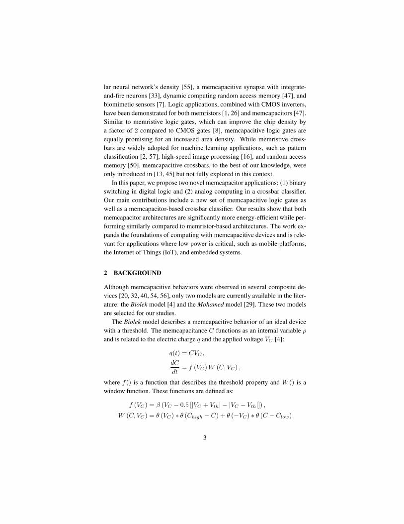
FIGURE 1
Charge-voltage response of the Biolek model [4] and the Mohamed model [29].
The Mohamed model depicts the memcapacitive response of a metal-dioxide
device. The correlations of the device states (x and m), the memcapacitance
C, and applied voltage v are as following [29]:
q(t) = C(x,m, v, t)v(t),
x =dx
dt= f (x, v, t) ,
m =dm
dt= f (m, v, t) ,
where x is the filament growth due to ion migrations between the metal-
dioxide gap, m is the cross section area of the filament, and f() is a window
function defined in [3]. The memcapacitance C is a function of the device’s
4
total capacitance. This function depends on the permittivity of the gap in-
sulator ε, the gap cross section A, and the maximum gap thickness d. The
derivatives of the state variables x and m model the growth/shrinkage of the
filament, which is controlled by the tunneling current it(t) and the capacitive
current ic(t) [29].
Fig. 1 shows the charge-voltage responses of the Biolek [4] model and the
Mohamed model [29]. As one can see, the responses follow a pinched hys-
teresis loop, which is the fundamental characteristic of a mem-device. The
threshold voltage of the Biolek model was set to 0.8V. The threshold voltage
was added to the original Mohamed model and the constants were modified
to deal with a low input frequency of 1Hz: KG = 0.4775,KS = 0.64, BG =
2.2475, BS = 2.75, xmin = 0.4, xmax = 0.9,mmin = 0.01,mmax =
0.9, d1 = 5× 10⁻¹⁰, and d2 = 5× 10⁻¹⁰.
3 PROPOSED MEMCAPACITIVE CIRCUITS
3.1 Memcapacitive Logic Gates
Logic gates form the fundamental building blocks of digital circuits and ar-
chitectures. It was proven that both memristors [25] and memcapacitive de-
vices [35] are capable of performing logic operations using material implica-
tions. Several studies have shown that logic gates can be realized with mem-
ristors [1, 8] and that such gates consume less power and allow for higher
integration densities than CMOS gates. The first design of memristive gates
was developed for fuzzy logic [24], which was extended to include sorting
networks [30]. It was show to be compatible with CMOS AND/OR func-
tionality [26]. The main idea for designing a memristive logic gate is based
on voltage division: several resistors connected in series can scale an ap-
plied voltage to different voltages according to their resistance values. Unlike
traditional fixed-value resistors, memristors have the ability to alter their re-
sistance to an ON state (low resistance) or OFF state (high resistance). The
voltages across them can therefore change dynamically. If the ON/OFF re-
sistance ratio is sufficiently large, each memristor in a memristive gate can
operate as a binary switch, analogous to a CMOS switch. Here, we apply the
same concept to memcapacitive gates since such devices, when connected in
series, can also scale voltages according to their dynamic capacitance.
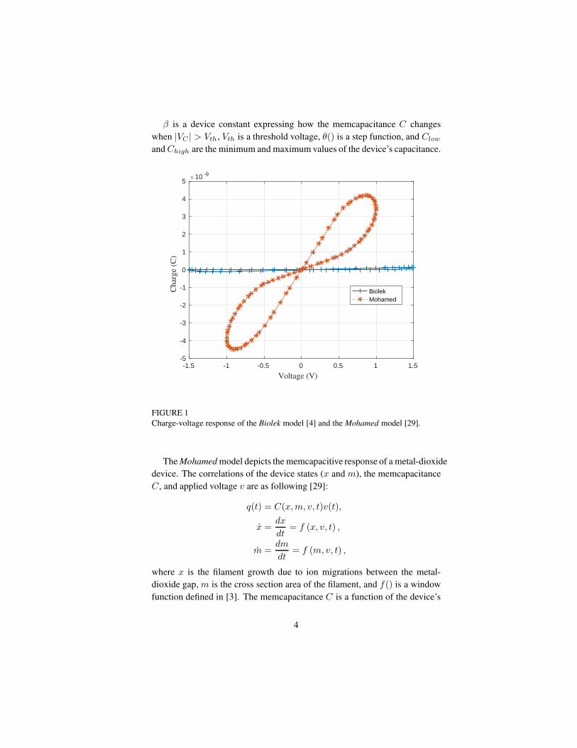
Considering the 2-input gate in Fig. 2, Mca and Mcb are in series with
respect to inputs a and b. The electric charge is the same for both devices:
5
a
Mcb
Mca
b
y
2-Input AND
b
Mcc
Mcb
c
y
3-Input AND
aMca
FIGURE 2
2-input and 3-input memcapacitive AND gates.
a
Mcb
Mca
b
y
2-Input OR
b
Mcc
Mcb
c
y
3-Input OR
aMca
FIGURE 3
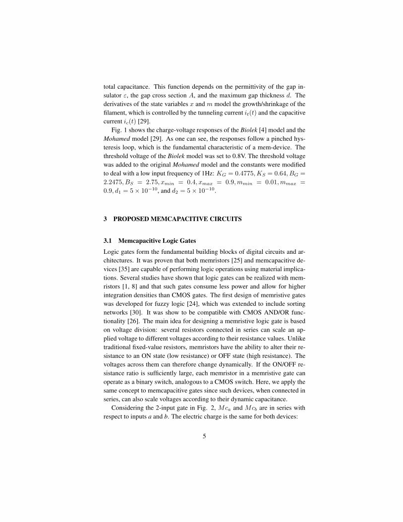
2-input and 3-input memcapacitive OR gates.
QMCa = QMCb,
(Va − Vy) ∗Mca = (Vy − Vb) ∗Mcb,
(Mca +Mcb) ∗ Vy = Va ∗Mca + Vb ∗Mcb,
Vy =Va ∗Mca + Vb ∗Mcb
Mca +Mcb. (4)
Assuming that Cmax >> Cmin with 0V for logic 0 and 1V for logic 1,
we consider four cases for the output Vy according to Eq. 4:
• V a = 0V, Vb = 0V : Vy = 0V
6

• V a = 0V, Vb = 1V : with their connection polarities, Mca is switched
to Cmax, Mcb is switched to Cmin, and the output voltage is:
Vy =Cmin
Cmax + Cmin
∗ Vb < VLH ≈ logic 0,
where VLH is the upper limit voltage for logic 0.
• V a = 1V, Vb = 0V : Mca is switched to Cmin, Mcb is switched to
Cmax, and the output voltage is:
Vy =Cmin
Cmin + Cmax
∗ Va < VLH ≈ logic 0
• V a = 1V, Vb = 1V : the output voltage is:
Vy =Mca +McbMca +Mcb
= 1V
The input combinations of a and b along with the output values of y con-
stitute the truth table of an AND gate.
Similarly, for the 2-input OR gate (Fig. 3) and from on the Eq. 4, we
consider four cases:
• V a = 0V, Vb = 0V : Vy = 0V
• V a = 0V, Vb = 1V : Mca is switched to Cmin, Mcb is switched to
Cmax, and the output voltage is:
Vy =Cmax
Cmin + Cmax
∗ Vb > VHL ≈ logic 1,
where VHL is the lower limit voltage for logic 1.
• V a = 1V, Vb = 0V : with their connection polarities, Mca is switched
to Cmax, Mcb is switched to Cmin, and the output voltage is:
Vy =Cmax
Cmax + Cmin
∗ Va > VHL ≈ logic 1
• V a = 1V, Vb = 1V : the output voltage is:
Vy =Mca +McbMca +Mcb
= 1V
7
Here, the input combinations of a and b and the corresponding output val-
ues y represent the truth table of an OR gate. Similarly, 3-input or 4-input
AND and OR memcapacitive gates can be built.
It is known [51] that any logic expression can be described as a combi-
nation of AND, OR, and NOT functions. The NOT function generally re-
quires an active element to complement its input signal. Since memcapac-
itive devices are passive, the NOT function cannot be implemented. As a
consequence, we still need to rely on a traditional CMOS inverter to obtain a
complete set of memcapacitive gates.
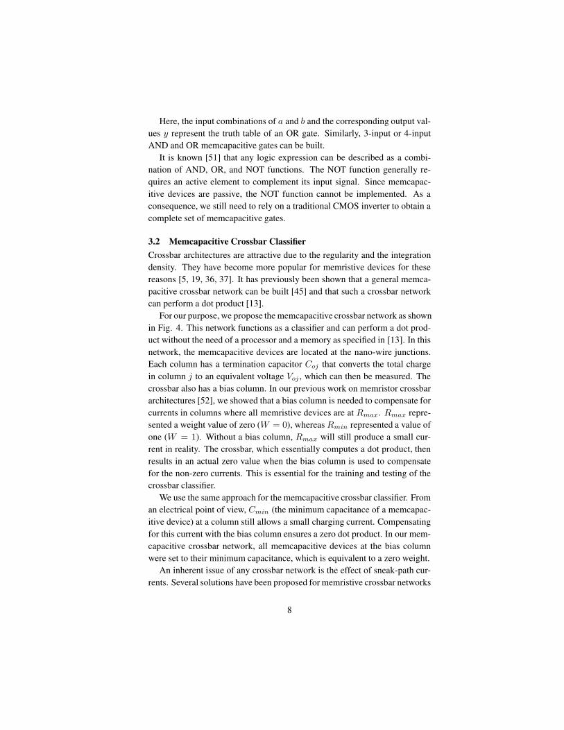
3.2 Memcapacitive Crossbar Classifier
Crossbar architectures are attractive due to the regularity and the integration
density. They have become more popular for memristive devices for these
reasons [5, 19, 36, 37]. It has previously been shown that a general memca-
pacitive crossbar network can be built [45] and that such a crossbar network
can perform a dot product [13].
For our purpose, we propose the memcapacitive crossbar network as shown
in Fig. 4. This network functions as a classifier and can perform a dot prod-
uct without the need of a processor and a memory as specified in [13]. In this
network, the memcapacitive devices are located at the nano-wire junctions.
Each column has a termination capacitor Coj that converts the total charge
in column j to an equivalent voltage Voj , which can then be measured. The
crossbar also has a bias column. In our previous work on memristor crossbar
architectures [52], we showed that a bias column is needed to compensate for
currents in columns where all memristive devices are at Rmax. Rmax repre-
sented a weight value of zero (W = 0), whereas Rmin represented a value of
one (W = 1). Without a bias column, Rmax will still produce a small cur-
rent in reality. The crossbar, which essentially computes a dot product, then
results in an actual zero value when the bias column is used to compensate
for the non-zero currents. This is essential for the training and testing of the
crossbar classifier.
We use the same approach for the memcapacitive crossbar classifier. From
an electrical point of view, Cmin (the minimum capacitance of a memcapac-
itive device) at a column still allows a small charging current. Compensating
for this current with the bias column ensures a zero dot product. In our mem-
capacitive crossbar network, all memcapacitive devices at the bias column
were set to their minimum capacitance, which is equivalent to a zero weight.
An inherent issue of any crossbar network is the effect of sneak-path cur-
rents. Several solutions have been proposed for memristive crossbar networks
8
memcapacitor
nano wire
desired path
undesired path
C11 C12 C13 C1n Cmin
C21
C31
C41
Cm1
v1
Co1
output
capacitor
v2
v3
v4
vm
Co2 Co3 Con Cob
Coj
Bias
column
Cmin
Cmin
Cmin
Cmin
FIGURE 4
Memcapacitive crossbar network. The role of the termination output capacitors
Co1, Co2, Co3, Co4, Con is to convert the total electric charge q in each column j
to a corresponding voltage Voj.
to overcome this problem: multistage readings [48], unfolded networks [28],
complimentary reading algorithm [18], virtual ground [53], or adapting three-
terminal devices [59]. From Fig. 4, the undesired paths allow additional
charge from other columns to go to output capacitors Co1 and Co2, which
then hold the total charge at only columns 1 and 2.
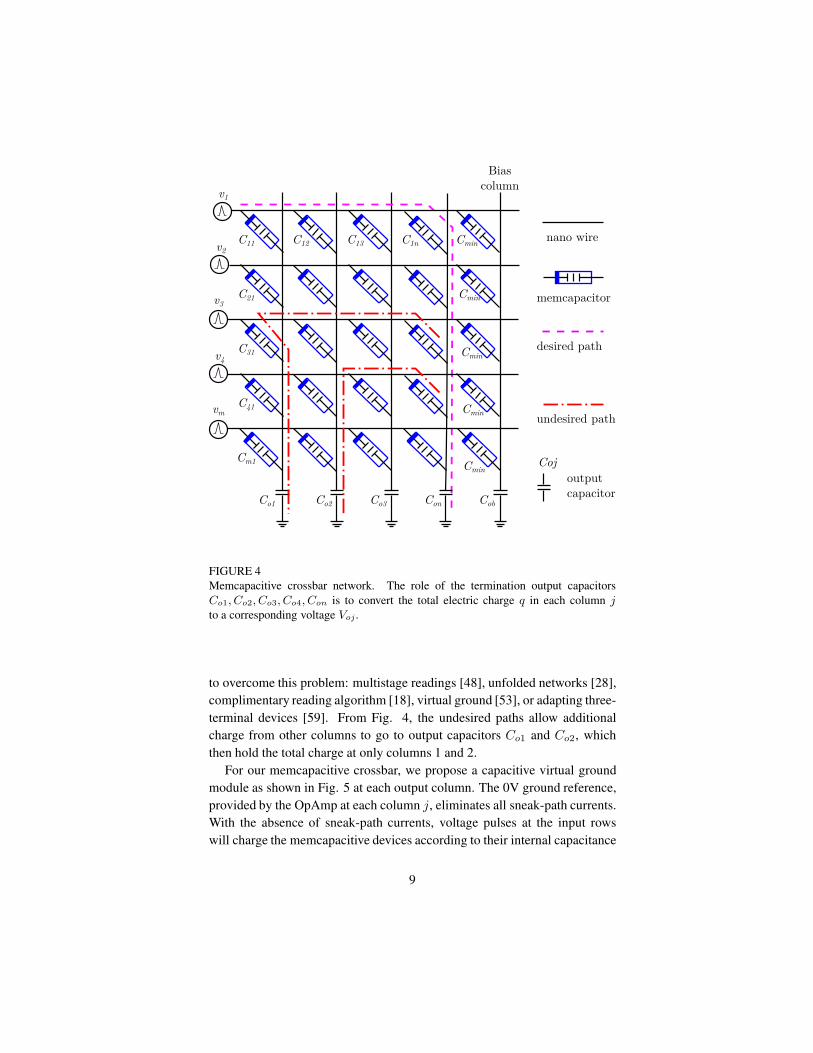
For our memcapacitive crossbar, we propose a capacitive virtual ground
module as shown in Fig. 5 at each output column. The 0V ground reference,
provided by the OpAmp at each column j, eliminates all sneak-path currents.
With the absence of sneak-path currents, voltage pulses at the input rows
will charge the memcapacitive devices according to their internal capacitance
9
Coj
+
-
the output
of column j
iCoj
Voj
FIGURE 5
Virtual ground module. The OpAmp provides a virtual ground. Charge from output
column j is compensated by charging or discharging currents through the capacitor
Coj .
states ρ. The total charge at a particular column j is then accumulated and
transferred to the output capacitor Coj in the virtual ground module. The total
charge Qj at column j is given by:
Qj =
m∑
i=1
qi,j − qbias, (5)
where qi,j is the electric charge stored in a memcapacitive device at the con-
nective junction (i, j) and qbias is the total electric charge of the bias column.
The subtractive term qbias ensures that the total charge Qj is zero when
all memcapacitive devices at column j are at their minimum capacitance.
Expanding and simplifying Eq. 5, the output voltage Voj at output column j
becomes:
Qj =
m∑
i=1
ViCi,j −
m∑
i=1
ViCmin
(−Voj)Coj =
m∑
i=1
ViCi,j −
m∑
i=1
ViCmin
−Voj =
m∑
i=1
Vi
(
Ci,j − Cmin
Coj
)
, (6)
where Ci,j is the capacitance of a memcapacitive device at junction (i, j),
bounded by the interval [Cmin, Cmax].
Eq. 6 shows that the output voltage at column j is proportional to the
device capacitance Ci,j and Cmin, the input voltage Vi, and the output ca-
pacitance Coj . The output voltage Voj is independent of charge Qj , the total
10
charge of all memcapacitive devices at column j. As a result, our memca-
pacitive crossbar does not suffer the large effect of charge leakage as reported
in [60] for a MOS-gated memristor array.
4 RESULTS
4.1 Mem-devices in Logic Applications
We used a pulse width tw and an amplitude vp to represent logic 1. To verify
the logic gates, pulses were generated from the signal sources to simulate
all the input states of a n-input gate. In addition, we measured the average
power consumption of the memcapacitive gates and compared the values with
equivalent memristive as well as CMOS gates.
According to [24], a valid output voltage of a memristive gate depends
significantly on the changing states (switching from RON to ROFF or vice
versa) of the device and a high ratio of ROFF and RON . This changing state
is linked to two physical factors of a memristive device, which vary from
device to device: threshold voltage vth and switching time ts. An applied
pulse has to be sufficiently large (vp > 2vth) and long (tw > ts) so that the
memristive devices can change their internal states and produce the correct
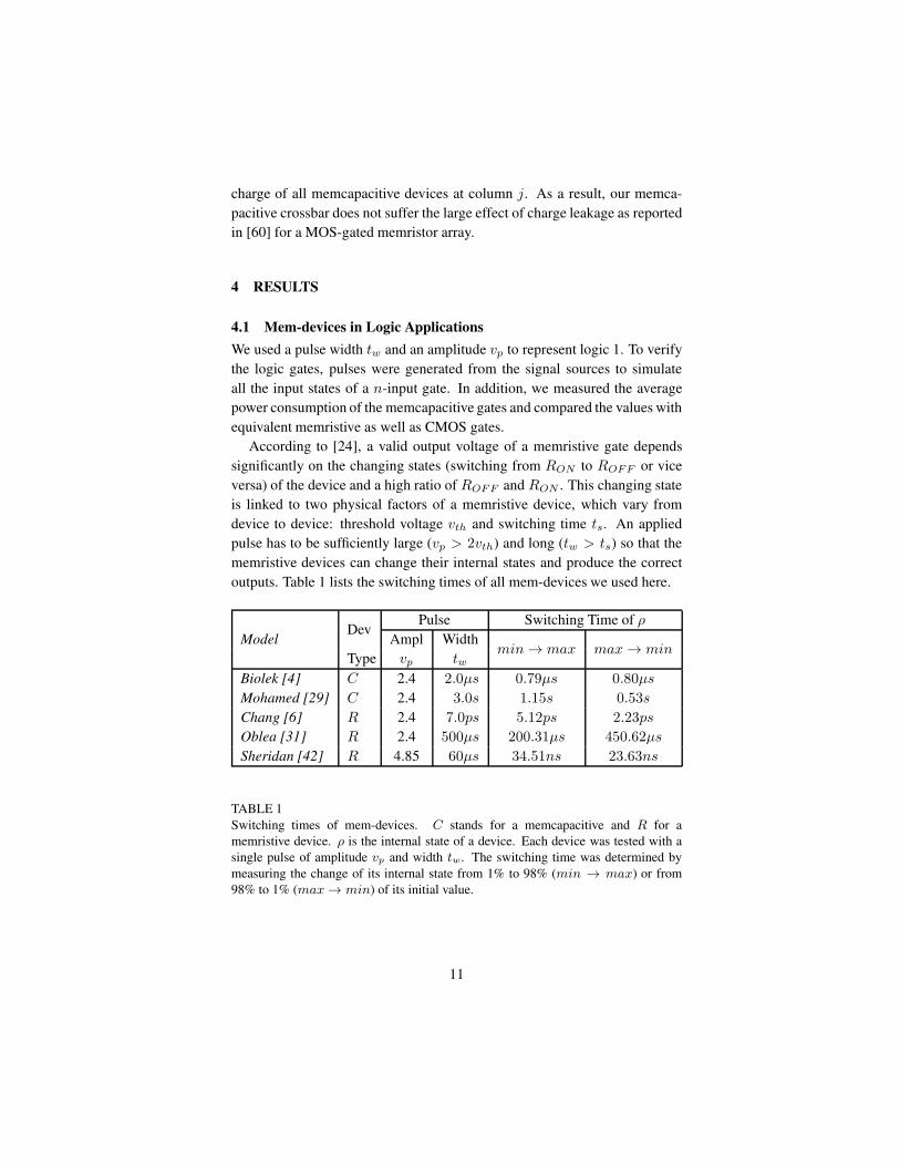
outputs. Table 1 lists the switching times of all mem-devices we used here.
ModelDev
Pulse Switching Time of ρ
Ampl Widthmin → max max → min
Type vp twBiolek [4] C 2.4 2.0µs 0.79µs 0.80µs
Mohamed [29] C 2.4 3.0s 1.15s 0.53s
Chang [6] R 2.4 7.0ps 5.12ps 2.23ps
Oblea [31] R 2.4 500µs 200.31µs 450.62µs
Sheridan [42] R 4.85 60µs 34.51ns 23.63ns
TABLE 1
Switching times of mem-devices. C stands for a memcapacitive and R for a
memristive device. ρ is the internal state of a device. Each device was tested with a
single pulse of amplitude vp and width tw. The switching time was determined by
measuring the change of its internal state from 1% to 98% (min → max) or from
98% to 1% (max → min) of its initial value.
11
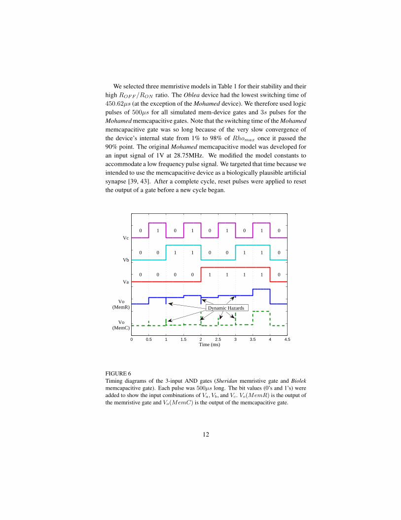
We selected three memristive models in Table 1 for their stability and their
high ROFF /RON ratio. The Oblea device had the lowest switching time of
450.62µs (at the exception of the Mohamed device). We therefore used logic
pulses of 500µs for all simulated mem-device gates and 3s pulses for the
Mohamed memcapacitive gates. Note that the switching time of the Mohamed
memcapacitive gate was so long because of the very slow convergence of
the device’s internal state from 1% to 98% of Rhomax once it passed the
90% point. The original Mohamed memcapacitive model was developed for
an input signal of 1V at 28.75MHz. We modified the model constants to
accommodate a low frequency pulse signal. We targeted that time because we
intended to use the memcapacitive device as a biologically plausible artificial
synapse [39, 43]. After a complete cycle, reset pulses were applied to reset
the output of a gate before a new cycle began.
0 0.5 1 1.5 2 2.5 3 3.5 4 4.5Time (ms)
0
0
0
0
0
1
0
1
0
0
1
1
1
0
0
1
0
1
1
1
0
1
1
1
0
0
0
Va
Vb
Vc
Dynamic HazardsVo
(MemR)
Vo(MemC)
FIGURE 6
Timing diagrams of the 3-input AND gates (Sheridan memristive gate and Biolek
memcapacitive gate). Each pulse was 500µs long. The bit values (0’s and 1’s) were
added to show the input combinations of Va, Vb, and Vc. Vo(MemR) is the output of
the memristive gate and Vo(MemC) is the output of the memcapacitive gate.
12
Since a mem-device inverter cannot be built, we used CMOS inverters
to build NAND, NOR, and XOR gates. For the full adder mem-device cir-
cuits, we utilized the mem-CMOS hybrid design of Cho et al. [8]. Their
results showed that multilayer memristor-MOS circuits can implement any
basic logic gate, such as AND, OR, NAND, NOR, and XOR.
Fig. 6 shows the timing diagram of the 3-input mem-device AND gates.
The bit values (0’s and 1’s) were added to show all input combinations.
Vo(MemR) and Vo(MemC) show the outputs for the memristor and the
memcapacitor gate respectively. Similar to memristive gates, our memcapac-
itive gates also showed dynamic hazards, a common phenomenon for mem-
ristive gates [26]. Dynamic hazards occurred when the mem-devices switched
their internal state ρ (from ρmin → ρmax and vice versa). Within these tran-
sition times, the output logic was undefined.
0 500 1000 1500 2000 2500 3000 3500 4000 4500−4
−3
−2
−1
0
1
2
3
Time (µs)
Vol
tage
(V
)
Vo(AND)
Vo(NOR)
1999 2000 2001 2002−4
−2
0
2
4
FIGURE 7
Dynamic logic hazards of 3-input memcapacitive AND(-) and NOR(–) gates using the
Biolek model. The inset shows the output values in the interval [1999µs, 2002µs].
With a 500µs pulse, the spike width of a logic hazard was about 0.8µs for the mem-
capacitive AND gate and about 0.6µs for the memcapacitive NOR gate.
13
The inset in Fig. 7 shows a dynamic hazard of the memcapacitive AND
and NOR gates in the interval [1999µs, 2002µs]. The spike width estimates
were 0.8µs and about 0.6µs for AND and NOR gates respectively. With a
pulse width of 500µs, dynamic hazards can be potentially avoided by adding
a time delay before reading the outputs. Another approach to remove dynamic
hazards is to add buffers or inverters along the signal paths to restore the logic
signals [26].
AND OR XOR Full Adder(FA)
10-1
100
101
102
103
104
105
106
Power (µW
)
Biolek (MemC)Mohamed (MemC)Chang (MemR)
Oblea (MemR)Sheridan (MemR)CMOS (32nm)
FIGURE 8
Power consumption of the mem-device logic and CMOS gates. The Biolek and Mo-
hamed gates are memcapacitive gates, the rest are memristive gates. The overall win-
ners for the mem-device gates were the Mohamed memcapacitive gates.
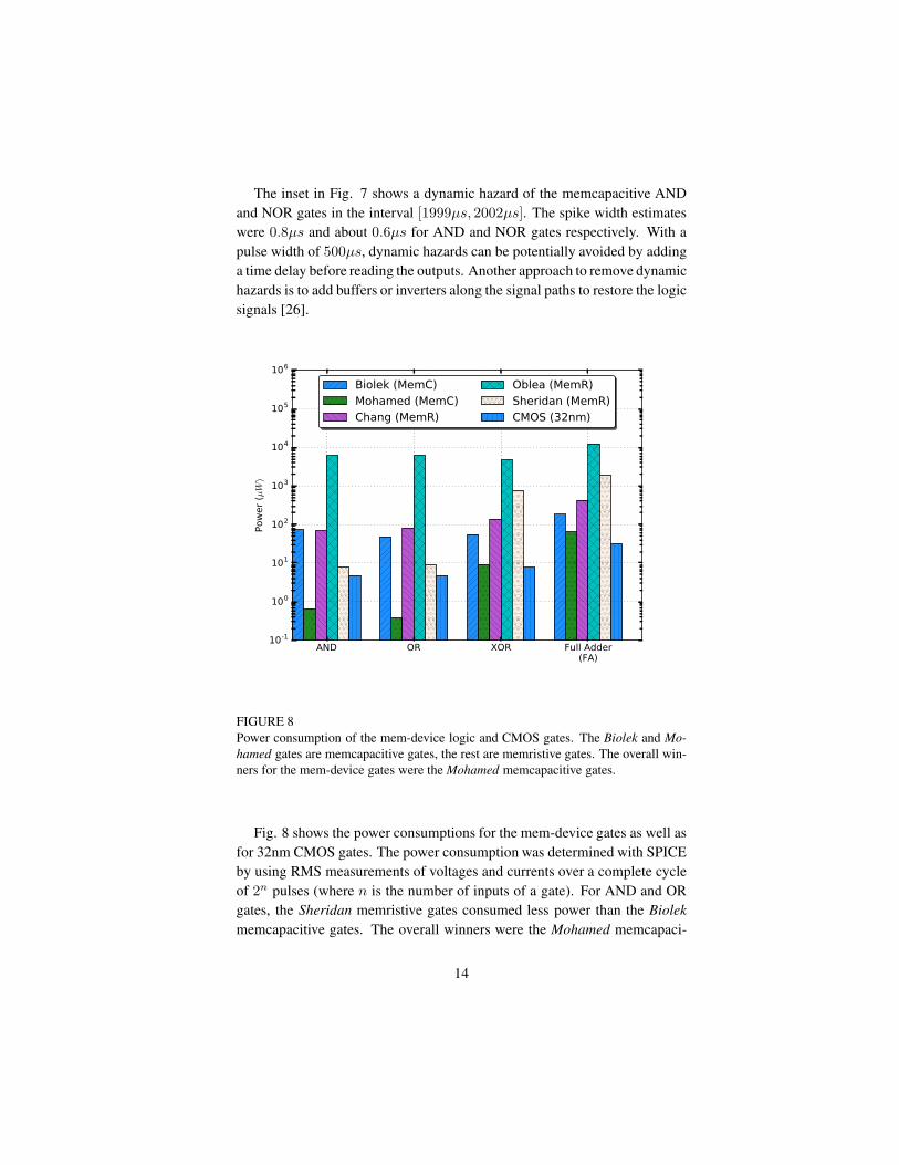
Fig. 8 shows the power consumptions for the mem-device gates as well as
for 32nm CMOS gates. The power consumption was determined with SPICE
by using RMS measurements of voltages and currents over a complete cycle
of 2n pulses (where n is the number of inputs of a gate). For AND and OR
gates, the Sheridan memristive gates consumed less power than the Biolek
memcapacitive gates. The overall winners were the Mohamed memcapaci-
14
tive gates. Furthermore, the Sheridan memristive gates required a 4.8V pulse
amplitude whereas the memcapacitive gates only needed 2.4V. A lower volt-
age can be an advantage for interfacing with CMOS devices that are operated
in a low-power mode [10].
The memcapacitive circuits outperformed the memristive circuits in terms
of power consumption for XOR and FA. Compared to CMOS gates, the Mo-
hamed memcapacitive AND and OR gates used less power. The memca-
pacitive XOR and full adder circuits, however, used more power than CMOS
circuits due the CMOS inverters that are needed to implement NOT functions.
In fact, the power consumptions of the CMOS inverters for the mem-device
XOR and full adder circuits contributed about 95% to the total power con-
sumptions.
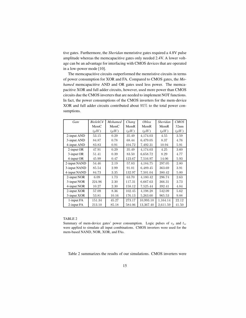
Gate BiolekC4 Mohamed Chang Oblea Sheridan CMOS
MemC MemC MemR MemR MemR 32nm
(µW ) (µW ) (µW ) (µW ) (µW ) (µW )
2-input AND 53.15 0.29 35.49 4,174.03 4.55 3.59
3-input AND 84.87 0.78 68.44 6,479.05 8.37 4.76
4-input AND 83.83 0.91 104.72 7,492.31 10.94 5.91
2-input OR 47.91 0.29 35.49 4,174.03 4.25 3.60
3-input OR 51.41 0.39 83.50 6,658.72 8.29 4.77
4-input OR 45.99 0.47 123.67 7,516.97 14.06 5.93
2-input NAND 54.46 2.19 57.83 4,184.75 297.05 2.80
3-input NAND 85.54 2.99 91.01 6,489.45 363.69 3.91
4-input NAND 84.73 3.35 132.97 7,501.04 380.42 5.00
2-input NOR 6.09 1.73 63.70 4,180.42 296.74 2.63
3-input NOR 224.96 2.30 117.31 6,667.63 366.31 3.73
4-input NOR 10.27 2.30 158.12 7,525.44 392.41 4.84
2-input XOR 57.09 8.36 102.45 4,198.28 542.09 5.62
3-input XOR 53.81 10.16 176.13 5,263.60 965.53 9.88
1-input FA 151.34 45.27 273.17 10,993.10 1,164.14 22.12
2-input FA 213.10 85.18 584.06 13,367.40 2,611.59 41.50
TABLE 2
Summary of mem-device gates’ power consumption. Logic pulses of vp and twwere applied to simulate all input combinations. CMOS inverters were used for the
mem-based NAND, NOR, XOR, and FAs.
Table 2 summarizes the results of our simulations. CMOS inverters were
15
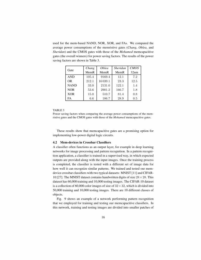
used for the mem-based NAND, NOR, XOR, and FAs. We compared the
average power consumptions of the memristive gates (Chang, Oblea, and
Sheridan) and the CMOS gates with those of the Mohamed memcapacitive
gates (the overall winners) for power saving factors. The results of the power
saving factors are shown in Table 3.
GateChang Oblea Sheridan CMOS
MemR MemR MemR 32nm
AND 105.4 9169.4 12.1 7.2
OR 212.1 16 039.1 23.3 12.5
NAND 33.0 2131.0 122.1 1.4
NOR 53.6 2901.2 166.7 1.8
XOR 15.0 510.7 81.4 0.8
FA 6.6 186.7 28.9 0.5
TABLE 3
Power saving factors when comparing the average power consumptions of the mem-
ristive gates and the CMOS gates with those of the Mohamed memcapacitive gates.
These results show that memcapacitive gates are a promising option for
implementing low-power digital logic circuits.
4.2 Mem-devices in Crossbar Classifiers
A classifier often functions as an output layer, for example in deep learning
networks for image processing and pattern recognition. In a pattern recogni-
tion application, a classifier is trained in a supervised way, in which expected
outputs are provided along with the input images. Once the training process
is completed, the classifier is tested with a different set of image data for
how well it can recognize similar patterns. We trained and tested our mem-
device crossbar classifiers with two typical datasets: MNIST [11] and CIFAR-
10 [27]. The MNIST dataset contains handwritten digits of size 28×28. This
dataset has 60,000 training and 10,000 testing images. The CIFAR-10 dataset
is a collection of 60,000 color images of size of 32×32, which is divided into
50,000 training and 10,000 testing images. There are 10 different classes of
objects.
Fig. 9 shows an example of a network performing pattern recognition
that we employed for training and testing our memcapacitive classifiers. In
this network, training and testing images are divided into smaller patches of
16
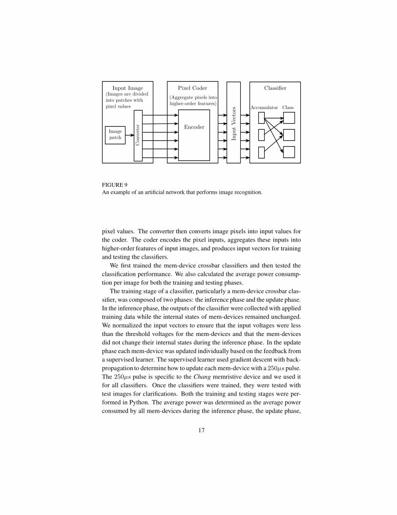
Pixel Coder ClassifierInput Image
(Aggregate pixels intohigher-order features)
Encoder
ClassAccumulator
Image
patchC
onver
ter
(Images are dividedinto patches withpixel values
Input
Vec
tors
FIGURE 9
An example of an artificial network that performs image recognition.
pixel values. The converter then converts image pixels into input values for
the coder. The coder encodes the pixel inputs, aggregates these inputs into
higher-order features of input images, and produces input vectors for training
and testing the classifiers.
We first trained the mem-device crossbar classifiers and then tested the
classification performance. We also calculated the average power consump-
tion per image for both the training and testing phases.
The training stage of a classifier, particularly a mem-device crossbar clas-
sifier, was composed of two phases: the inference phase and the update phase.
In the inference phase, the outputs of the classifier were collected with applied
training data while the internal states of mem-devices remained unchanged.
We normalized the input vectors to ensure that the input voltages were less
than the threshold voltages for the mem-devices and that the mem-devices
did not change their internal states during the inference phase. In the update
phase each mem-device was updated individually based on the feedback from
a supervised learner. The supervised learner used gradient descent with back-
propagation to determine how to update each mem-device with a 250µs pulse.
The 250µs pulse is specific to the Chang memristive device and we used it
for all classifiers. Once the classifiers were trained, they were tested with
test images for clarifications. Both the training and testing stages were per-
formed in Python. The average power was determined as the average power
consumed by all mem-devices during the inference phase, the update phase,
17
Chang(Memristor)
Oblea(Memristor)
Biolek(Memcapacitor)
Mohamed(Memcapacitor)
0
20
40
60
80
100
Perform
ance (%)
Performance (%) Avg Power (mW)
10-5
10-4
10-3
10-2
10-1
100
101
102
103
104
Power (m
W)
FIGURE 10
Classification performance and power consumption of the mem-device classifiers for
the MNIST dataset. The power measurements do not include the power consumption
of the virtual ground modules.
and the testing phase.
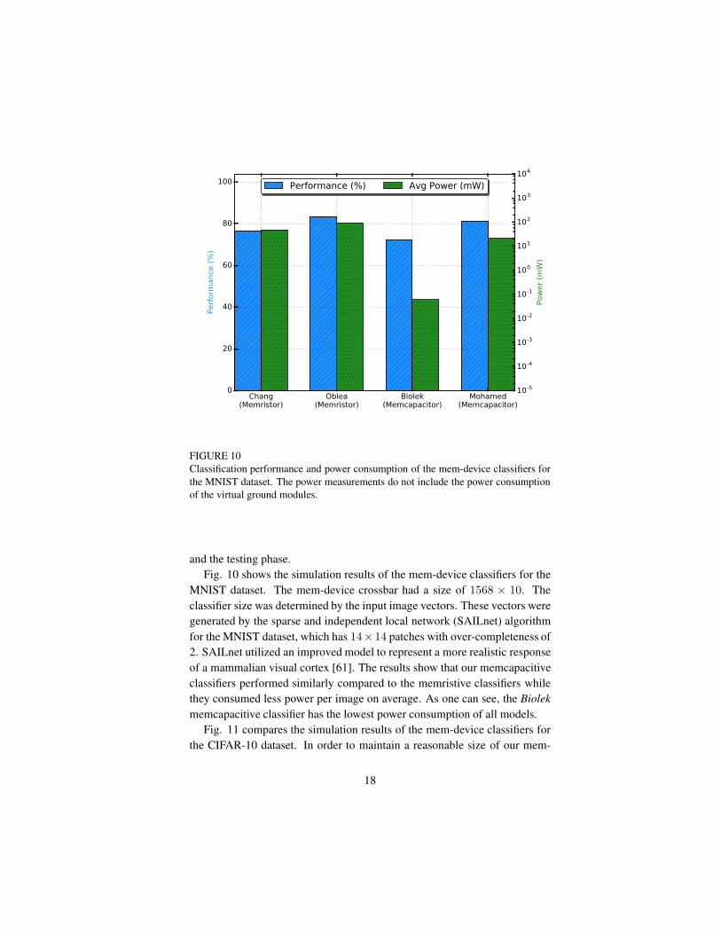
Fig. 10 shows the simulation results of the mem-device classifiers for the
MNIST dataset. The mem-device crossbar had a size of 1568 × 10. The
classifier size was determined by the input image vectors. These vectors were
generated by the sparse and independent local network (SAILnet) algorithm
for the MNIST dataset, which has 14× 14 patches with over-completeness of
2. SAILnet utilized an improved model to represent a more realistic response
of a mammalian visual cortex [61]. The results show that our memcapacitive
classifiers performed similarly compared to the memristive classifiers while
they consumed less power per image on average. As one can see, the Biolek
memcapacitive classifier has the lowest power consumption of all models.
Fig. 11 compares the simulation results of the mem-device classifiers for
the CIFAR-10 dataset. In order to maintain a reasonable size of our mem-
18
Chang(Memristor)
Oblea(Memristor)
Biolek(Memcapacitor)
Mohamed(Memcapacitor)
0
10
20
30
40Perform
ance (%)
Performance (%) Avg Power (mW)
10-5
10-4
10-3
10-2
10-1
100
101
102
103
104
105
Power (m
W)
FIGURE 11
Classification performance and power consumption of the mem-device classifiers for
the CIFAR-10 dataset. The power measurements do not include the power consump-
tion of the virtual ground modules.
device classifiers (such as 4508×10), the color images were converted to gray
scale images for training and testing. Furthermore, a whitening process was
applied to the input images in order to reduce the highly correlated adjacent
pixels, which showed to improve both the training time and performance [14].
The length of each input image vector determined the size of the classifiers.
For CIFAR-10, the SAILnet algorithm generated the input vectors of 16× 16
patches and an over-completeness of 2.
As one can see from Fig. 11, the memcapacitive classifiers did not reach
the performance of memristive classifiers, but they consumed less power. The
performance of memcapacitive classifiers correlated directly with the setting
parameters (the learning rate α, the update pulse width tw, the update pulse
amplitude vw, and the offset voltage voffset) during the training phase. These
parameters were chosen based on experiments.
19
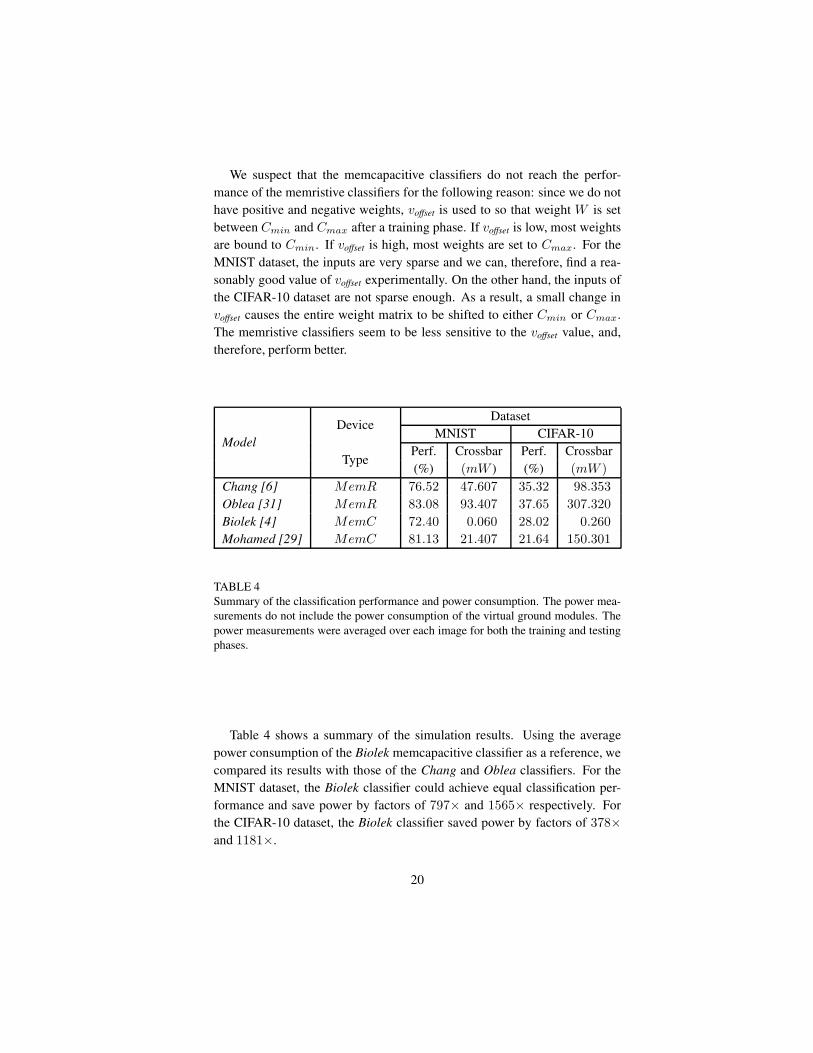
We suspect that the memcapacitive classifiers do not reach the perfor-
mance of the memristive classifiers for the following reason: since we do not
have positive and negative weights, voffset is used to so that weight W is set
between Cmin and Cmax after a training phase. If voffset is low, most weights
are bound to Cmin. If voffset is high, most weights are set to Cmax. For the
MNIST dataset, the inputs are very sparse and we can, therefore, find a rea-
sonably good value of voffset experimentally. On the other hand, the inputs of
the CIFAR-10 dataset are not sparse enough. As a result, a small change in
voffset causes the entire weight matrix to be shifted to either Cmin or Cmax.
The memristive classifiers seem to be less sensitive to the voffset value, and,
therefore, perform better.
Model
DeviceDataset
MNIST CIFAR-10
TypePerf. Crossbar Perf. Crossbar
(%) (mW ) (%) (mW )
Chang [6] MemR 76.52 47.607 35.32 98.353
Oblea [31] MemR 83.08 93.407 37.65 307.320
Biolek [4] MemC 72.40 0.060 28.02 0.260
Mohamed [29] MemC 81.13 21.407 21.64 150.301
TABLE 4
Summary of the classification performance and power consumption. The power mea-
surements do not include the power consumption of the virtual ground modules. The
power measurements were averaged over each image for both the training and testing
phases.
Table 4 shows a summary of the simulation results. Using the average
power consumption of the Biolek memcapacitive classifier as a reference, we
compared its results with those of the Chang and Oblea classifiers. For the
MNIST dataset, the Biolek classifier could achieve equal classification per-
formance and save power by factors of 797× and 1565× respectively. For
the CIFAR-10 dataset, the Biolek classifier saved power by factors of 378×
and 1181×.
20
5 DISCUSSION
As it was shown in Table 1, the Oblea device has the slowest settling time with
the exception of the Mohamed device. As a result, we used 500µs pulses
to test all mem-device logic gates. Operating mem-device logic gates with
500µs pulses is quite slow compared to CMOS logic gates. However, the
Biolek memcapacitive logic gates with a smaller switching time are capable
to operate with 2µs pulses.
Both memristive and memcapacitive gates suffered the effect of dynamic
hazards. Dynamic hazards occurred when the mem-devices of a gate switched
their internal states. Therefore, a delay time was required before the gate’s
output could be read. This delay time is similar to the setup time in a CMOS
gate, although the CMOS setup time is much smaller. Recent studies have
shown that new memristive devices can switch their internal states much
faster (in the range of ns and ps) [9, 21]. A faster switching time would
imply less dynamic hazards.
The Mohamed memcapacitive XOR and the full adder circuits did not out-
perform the CMOS circuits in terms of power consumption. However, about
95% of the power consumption was due to the CMOS inverters and transistors
that are required for the gates in addition to the mem-devices.
The performance of the memcapacitive classifiers depends on how the
memcapacitive devices are updated. The process involves setting four pa-
rameters: the learning rate α, the update pulse width tw, the update pulse
amplitude vw, and the offset voltage voffset. These parameters were based on
experiments. A systematic exploration of the parameter space is beyond the
scope of this paper. We expect that the classification performance can be
further increased with better parameters.
Moreover, virtual ground modules played an essential role in alleviating
the effect of sneak-path currents within the crossbar networks. We have left
out the power figures for these modules because they are highly technology-
dependent.
6 CONCLUSION
Our work has shown that low-power memcapacitive logic circuits can be im-
plemented. The memcapacitive gates consumed about 7× less power com-
pared to memristive logic gates. The lack of a mem-inverter makes the pos-
sible logical basis incomplete. The inverter operation, by its nature, requires
an active element to reverse its input signal, which cannot be realized by pas-
21
sive mem-devices. Used for classifiers, memcapacitive devices were shown
to reduce the power consumption by a factor of 1, 500× for MNIST and a fac-
tor of 1, 000× for CIFAR-10. For the classifier, we relied on virtual ground
modules, which remove the effects of sneak-path currents, but consume sig-
nificant power. Finding other options to eliminate sneak-path currents without
the need of virtual ground modules could further lower the power consump-
tion.
7 ACKNOWLEDGMENTS
This work was supported by the Defense Advanced Research Projects Agency
(DARPA) under award # HR0011-13-2-0015. The views expressed are those
of the author(s) and do not reflect the official policy or position of the De-
partment of Defense or the U.S. Government. Approved for Public Release,
Distribution Unlimited.
The authors also thank Jens Burger and Walt Woods for the helpful dis-
cussions.
REFERENCES
[1] B. Abdoli, A. Amirsoleimani, J. Shamsi, K. Mohammadi, and A. Ahmadi. (May 2014).
A novel CMOS-memristor based inverter circuit design. In 2014 22nd Iranian Conference
on Electrical Engineering (ICEE), pages 371–276.
[2] F. Alibart, E. Zamanidoost, and D. B. Strukov. (2012). Pattern classification by memristive
crossbar circuits using ex situ and in situ training. Nature communications, 4(2072):2072–
2072.
[3] D. Biolek, V. Biolkova, and Z. Biolek. (June 2009). Spice model of memristor with
nonlinear dopant drift. Radioengineering, 18(2):210–214.
[4] D. Biolek, M. Di Ventra, and Y. V. Pershin. (July 2013). Reliable SPICE simulations of
memristors, memcapacitors and meminductors. Radioengineering, 22(4):945–968.
[5] J. Burger and C. Teuscher. (July 2014). Volatile memristive devices as short-term memory
in a neuromorphic learning architecture. In Proceedings of the 2014 IEEE/ACM Interna-
tional Symposium on Nanoscale Architectures, pages 104–109.
[6] T. Chang, Y. Yang, and W. Lu. (2013). Building Neuromorphic Circuits with Memristive
Devices. IEEE Circuits and Systems Magazine, 13(2):56–73.
[7] E. T. Chen, J. Thornton, and C. Jr. Mulchi. (2014). Mapping Circular Current for a Single
Brain Cancer Cell’s Spatial-Temporal Orientations Based on a Memristor/Memcapacitor.
Sensors & Transducers, 183(12):72–83.
[8] K. Cho, S. Lee, and K. Eshraghian. (2015). Memristor-CMOS logic and digital computa-
tional components. Microelectronics Journal, 46(3):214–220.
[9] B. J. Choi, A. C. Torrezan, J. P. Strachan, P.G. Kotula, A.J. Lohn, M. J. Marinella, Z. Li,
R. S. Williams, and J. J. Yang. (2016). High-speed and low-energy nitride memristors.
Advanced Functional Materials, 26(29):5290–5296.
22
[10] S. Das, R. Prakash, A. Salazar, and J. Appenzeller. (2014). Toward low-power electronics:
tunneling phenomena in transition metal dichalcogenides. American Chemical Society
Nano, 8(2):1681–1689.
[11] T. Domhan, J. T. Springenberg, and F. Hutter. (2015). Speeding up automatic hyper-
parameter optimization of deep neural networks by extrapolation of learning curves. In
Proceedings of the 24th International Joint Conference on Artificial Intelligence (IJCAI),
pages 3460–3468.
[12] H. Esmaeilzadeh, E. Blem, R. St. Amant, K. Sankaralingam, and D. Burger. (2013). Power
challenges may end the multicore era. Communications of the ACM, 56(2):93–102.
[13] N. Ge, J. P. Strachan, J. Yang, and M. Hu, (May 6 2016). Memcapacitive cross-bar array
for determining a dot product. Patent WO2016068886A1.
[14] B. Hariharan, J. Malik, and D. Ramanan. (2012). Discriminative decorrelation for cluster-
ing and classification. In European Conference on Computer Vision, pages 459–472.
[15] M. Hu, H. Li, Y. Chen, Q. Wu, G. Rose, and R. Linderman. (2014). Memristor Crossbar-
Based Neuromorphic Computing System: A Case Study. IEEE Transactions on Neural
Networks and Learning Systems, 25(10):1864–1878.
[16] X. Hu, S. Duan, L. Wang, and X. Liao. (2012). Memristive crossbar array with applications
in image processing. Science China Information Sciences, 55(2):461–472.
[17] G. Indiveri, B. Linares-Barranco, R. Legenstein, G. Deligeorgis, and T. Prodromakis. (2013).
Integration of nanoscale memristor synapses in neuromorphic computing architectures.
Nanotechnology, 24(38):384010.
[18] C-M. Jung, J-M. Choi, and K-S. Min. (2012). Two-step write scheme for reducing sneak-
path leakage in complementary memristor array. IEEE Transactions on Nanotechnology,
11(3):611–618.
[19] I. Kataeva, F. Merrikh-Bayat, E. Zamanidoost, and D. Strukov. (2015). Efficient training
algorithms for neural networks based on memristive crossbar circuits. In 2015 Interna-
tional Joint Conference on Neural Networks (IJCNN), pages 1–8.
[20] A. K. Khan and B. H. Lee. (2016). Monolayer MoS2 metal insulator transition based
memcapacitor modeling with extension to a ternary device. AIP Advances, 6(9):095022.
[21] H.D. Kim, K. H. Kim, H.M. An, and T. G. Kim. (2015). Charge-trap flash memory
using zirconium-nitride-based memristor switches. Journal of Physics D: Applied Physics,
48(44):445102.
[22] S. Kim, J. Zhou, and W. Lu. (2014). Crossbar RRAM Arrays: Selector Device Require-
ments During Write Operation. Electron Devices, IEEE Transactions on, 61(8):2820–
2826.
[23] Y. Kim, Y. Zhang, and P. Li. (2015). A Reconfigurable Digital Neuromorphic Processor
with Memristive Synaptic Crossbar for Cognitive Computing. ACM Journal on Emerging
Technologies in Computing Systems, 11(4):1–25.
[24] M. Klimo and O. Such. (2011). Memristors can implement fuzzy logic. arXiv preprint
arXiv:1110.2074.
[25] S. Kvatinsky, G. Satat, N. Wald, E. G. Friedman, A. Kolodny, and U. C. Weiser. (2014).
Memristor-based material implication (imply) logic: design principles and methodologies.
IEEE Transactions on Very Large Scale Integration (VLSI) Systems, 22(10):2054–2066.
[26] S. Kvatinsky, N. Wald, G. Satat, A. Kolodny, U. C. Weiser, and E. G Friedman. (2012).
MRL - Memristor Ratioed Logic. In 2012 13th International Workshop on Cellular
Nanoscale Networks and their Applications, pages 1–6.
23
[27] CY. Lee, S. Xie, P. Gallagher, Z. Zhang, and Z. Tu. (2015). Deeply-Supervised Nets. In
The 18th International Conference on Artificial Intelligence and Statistics, page 6.
[28] H. Manem, G. S. Rose, X. He, and W. Wang. (May 2010). Design considerations for
variation tolerant multilevel CMOS/Nano memristor memory. In Proceedings of the ACM
Great Lakes Symposium on VLSI, pages 287–292.
[29] M. G. A. Mohamed, H. Kim, and T. Cho. (2014). Modeling of Memristive and Memca-
pacitive Behaviors in Metal-Oxide Junctions. The Scientific World Journal, 2015:910126–
910126.
[30] L. Nielen, S. Ohm, O. Such, M. Klimo, R. Waser, and E. Linn. (2016). Memristive
sorting networks enabled by electrochemical metallization cells. International Journal of
Unconventional Computing, 12(4):303–317.
[31] A. S. Oblea, A. Timilsina, D. Moore, and K. A. Campbell. (July 2010). Silver chalcogenide
based memristor devices. In The 2010 International Joint Conference on Neural Networks
(IJCNN), pages 1–3.
[32] M. Park, S. Park, and K-H. Yoo. (2016). Multilevel Nonvolatile Memristive and Mem-
capacitive Switching in Stacked Graphene Sheets. ACS Applied Materials & Interfaces,
8(22):14046–14052.
[33] Y. V. Pershin and M. Di Ventra. (2014). Memcapacitive neural networks. Electronics
Letters, 50(3):141–143.
[34] Y. V. Pershin, V. A. Slipko, and M. Di Ventra. (2015). Reconfigurable transmission lines
with memcapacitive materials. Applied Physics Letters, 107(25):253101.
[35] Y. V. Pershin, F. L. Traversa, and M. Di Ventra. (2015). Memcomputing with membrane
memcapacitive systems. Nanotechnology, 26(22):225201.
[36] P. Pouyan, E. Amat, and A. Rubio. (2015). Statistical lifetime analysis of memristive
crossbar matrix. In 2015 10th International Conference on Design Technology of Inte-
grated Systems in Nanoscale Era (DTIS), pages 1–6.
[37] M. Prezioso, F. Merrikh-Bayat, B.D. Hoskins, G.C. Adam, K. K. Likharev, and D. B.
Strukov. (2015). Training and operation of an integrated neuromorphic network based on
metal-oxide memristors. Nature, 521(7550):61–64.
[38] D. Querlioz, WS. Zhao, P. Dollfus, J-O. Klein, O. Bichler, and C. Gamrat. (2012). Bioin-
spired networks with nanoscale memristive devices that combine the unsupervised and
supervised learning approaches. In Proceedings of the 2012 IEEE/ACM International
Symposium on Nanoscale Architectures, pages 203–210.
[39] M. A. Rutherford, N. M. Chapochnikov, and T. Moser. (2012). Spike encoding of neu-
rotransmitter release timing by spiral ganglion neurons of the cochlea. The Journal of
Neuroscience, 32(14):4773–4789.
[40] S. Sarma, B. M. Mothudi, and M. S. Dhlamini. (2016). Observed coexistence of memris-
tive, memcapacitive and meminductive characteristics in polyvinyl alcohol/cadmium sul-
phide nanocomposites. Journal of Materials Science: Materials in Electronics, 27(5):4551–
4558.
[41] T. Serrano-Gotarredona, T. Masquelier, T. Prodromakis, G. Indiveri, and B. Linares-Barranco.
(2013). STDP and STDP variations with memristors for spiking neuromorphic learning
system. Frontiers in Neuroscience, 7(2):1–15.
[42] P. Sheridan, K.H. Kim, S. Gaba, T. Chang, L. Chen, and W. Lu. (2011). Device and SPICE
modeling of RRAM devices. Nanoscale, 3(9):3833.
[43] S. Song, J. Li, L. Zhu, L. Cai, Q. Xu, C. Ling, Y. Su, and Q. Hu. (2012). Irregular Ca2+
oscillations regulate transcription via cumulative spike duration and spike amplitude. Jour-
nal of Biological Chemistry, 287(48):40246–40255.
24
[44] D. B. Strukov, G. S. Snider, D. R. Stewart, and R. S. Williams. (May 2008). The missing
memristor found. Nature, 453(7191):80–83.
[45] D. B. Strukov, G. S. Snider, and R. S. Williams, (December 10 2013). Capacitive crossbar
arrays. US Patent 8,605,488.
[46] T. M. Taha, R. Hasan, and C. Yakopcic. (2014). Memristor crossbar based multicore
neuromorphic processors. In 2014 27th IEEE International System-on-Chip Conference
(SOCC), pages 383–389.
[47] F. L. Traversa, F. Bonani, Y. V. Pershin, and M. Di Ventra. (2014). Dynamic computing
random access memory. Nanotechnology, 25(28):285201.
[48] P. O. Vontobel, W. Robinett, Philip J. Kuekes, D. R. Stewart, J. Straznicky, and R. S.
Williams. (2009). Writing to and reading from a nano-scale crossbar memory based on
memristors. Nanotechnology, 20(42):425204.
[49] I. Vourkas and G. Ch. Sirakoulis. (2016). Emerging memristor-based logic circuit design
approaches: A review. IEEE Circuits and Systems Magazine, 16(3):15–30.
[50] I. Vourkas, D. Stathis, G. Ch. Sirakoulis, and S. Hamdioui. (2016). Alternative archi-
tectures toward reliable memristive crossbar memories. IEEE Transactions on Very Large
Scale Integration (VLSI) Systems, 24(1):206–217.
[51] A. N. Whitehead and B. Russell. (1912). Principia mathematica, volume 2. University
Press.
[52] W. Woods, M. M. A Taha, D. Tran, J. Burger, and C. Teuscher. (2015). Memristor Panic -
A Survey of Different Device Models in Crossbar Architectures. Nanoscale Architectures
(NANOARCH), 2015 IEEE/ACM International Symposium on, pages 106–111.
[53] C. Yakopcic, R. Hasan, T. M. Taha, M. R. McLean, and D. Palmer. (2014). Efficacy of
memristive crossbars for neuromorphic processors. In 2014 International Joint Conference
on Neural Networks (IJCNN), pages 15–20.
[54] P. Yang, Y. J. Noh, Y-J. Baek, H. Zheng, C. J. Kang, H. H. Lee, and T-S. Yoon. (2016).
Memcapacitive characteristics in reactive-metal (Mo, Al)/HfOX /n-Si structures through
migration of oxygen by applied voltage. Applied Physics Letters, 108(5):052108.
[55] S. Yi, J. Zhenzhen, W. Xiaoping, and L. Yang. (2015). Two novel cellular neural networks
based on mem-elements. In Control Conference (CCC), 2015 34th Chinese, pages 3452–
3456.
[56] T. You, L. P. Selvaraj, H. Zeng, W. Luo, N. Du, D. Burger, I. Skorupa, S. Prucnal, A. Law-
erenz, and T. Mikolajick. (March 2016). An Energy-Efficient BiFeO3-Coated Capacitive
Switch with Integrated Memory and Demodulation Functions. Advanced Electronic Mate-
rials, 2(3).
[57] E. Zamanidoost, F. M. Bayat, D. Strukov, and I. Kataeva. (2015). Manhattan rule training
for memristive crossbar circuit pattern classifiers. In Intelligent Signal Processing (WISP),
2015 IEEE 9th International Symposium on, pages 1–6.
[58] J. Zhou, K-H. Kim, and W. Lu. (2014). Crossbar RRAM arrays: Selector device require-
ments during read operation. Electron Devices, IEEE Transactions on, 61(5):1369–1376.
[59] M. A. Zidan, H. A. H. Fahmy, M. M. Hussain, and K. N. Salama. (2013). Memristor-based
memory: The sneak paths problem and solutions. Microelectronics Journal, 44(2):176–
183.
[60] M. A. Zidan, H. Omran, A. Sultan, H. A. H. Fahmy, and K. N. Salama. (2015). Compen-
sated readout for high-density mos-gated memristor crossbar array. IEEE Transactions on
Nanotechnology, 14(1):3–6.
[61] J. Zylberberg, J. T. Murphy, and M. R. DeWeese. (2011). A Sparse Coding Model with
Synaptically Local Plasticity and Spiking Neurons Can Account for the Diverse Shapes of
V1 Simple Cell Receptive Fields. PLOS Computational Biology, 7(10):1–12.
25