Embed Size (px)
Citation preview

__
AGENCY FOR INTERNATIONAL DEVELOPMENT WASHINGTON D C 2(1523
DATE I
MEMORANDUM
TO AIDPPCCDIEDI room 209 SA-18
FROM AIDSCI Victoria Ose
SUBJECT Transmittal of AIDSCI Progress Report(s)
Attached for permanent retentionpoper disposition is the following
AIDSCI Progress Report No t i
Attachment
PROGRESS REPORT
ON
PROJECT N e20A4 DIGITAL INFORMATION TRANSMI ON LECTRIC POWER LINES
PREPARED BY
PROF S YUNKAP KWANKAM
AULJTOMATrION AND CONTROL LABORTORY
Ecole Nationale Superieure PolytechnigseHP 8390 YAOUNDECameroon Tel (237) 32-12-26 Telex 8384 N
September 1988
Recd inSC NOV 4 1988
INTRODUCTION
The original project document called for the project tpexpire on October 31 1987 However a second ammendment to this document extended the life of the project to December 31 1988 Project activities were then rescheduled as shown in the prgress report of April 1987
PROGRESS MADE
As indicated in the progress report of April 1937 theencoder and decoder systems were implemeted usingmicroprocessors specifically the Motorola MEK6802D5 singleshyboard microcomputer This enabled easy modification of system parameters such as suppression time and the study of their effect cn detectability and spectral distortion However programming the microprocessor to implement various encoding and detection schemes remained difficult because code had to be entered in machine language using a monitor program
To facilitate the software development aspects of the project the system has been implemented using a more advanced single-board microcomputer the MICROMEGAS This module which uses the 6809 microprocessor permits software development in assembler language through the use of a personal computer system
In July 1988 a request was made to seek authorization for modification to the project objectives Our experiencein the laboratory and subsequent discussions with thenational electric utility in Cameroon (SONEL) had led us to conclude that the greatest impact of the project will be its use for remote meter reading Based on this conclusion work has been undertaken to develop the rmote meter readingapplication of the technclogy To this end an interface between a standard electric utility meter of the type used in Cameroon and the encoderdecoder unit developed earlier has been realized Software drivers have been written to test this interface (See thesis by Joseph Ngaku June 1988) Algorithms for speeding up the read process have been examined (See thesis by Gilbert Fonkwo June 1988)
EXPENDITURE
Out of a total budget of One hundred thirteen thousand five hundred forty-four dollars ($113544) a total of about sisty-eight thousand four hundred and four dollars ($68404)
2
has been disbursed The expenditure breakdown is as
follows
- Equipment - $31129 +
- Technician salaries - $ 9192 +
- Overhead - $ 2455 +
Thus a total of forty-five thousand hundredone fortydollars ($45140) remains unspent
OUTPUT SO FAR
In addition to the outputs indicated in the progressreport of April 1987 the following quantifiable outputshave been obtained
- 1 paper Parameter Bounds for a New Digital Power Line Communication Technique Using WaveformModification Technology and Development Vol 3 no 1 pp 33 - 40 June 1987
- an electric utility meter interface and driver for remote pickup of meter reading
Unquantifiable outputs include a significant amount ofinstitution strengthening The facilities provided throughthe project are the main equipment support of the Automationand Control Laboratory (ACL) of Ecolethe NationaleSuperieure Polytechnique (School of Engineering) of theUniversity of Yaounde During the 1987-88 academic year atotal of nine student engineer theses were undertaken underthe auspices of the ACL The Laboratory also sponsored student final-year projects in the senior technician program
DIFFICULTIES ENCOUNTERED
The project continues to be plagued by pproblems oflogistical support as described in the April 1987 report
Technical problems encountered center around parallelsignal injection using a shunt element as opposed to aseries pass element of the implementation currently in usein the laboratory A series pass element (an SCR in thiscase) requires that firing pulses be provided even whenthere is no data transmission on the line This representsoverhead on the data transmi sion scheme Secondly the loadcurrent in this case flows through the SCR Thus should thedata transmission system fail to provide firing pulsesshould the SCR fail
or in the open circuit condition power is
cut off from all loads downstream
3
A shunt element (a transistor in our case) eliminatesthe overhead incurred with a series pass element Moreimportant any failure of the data transmission system or ofthe transistor in the open circuit condition will not resultin loss of power for downstream loads
For these reasons and the fact that a shunt element ismuch better suited to use of this technology for remotemeter reading we are vigorously pursuing the development of an injection method using a shunt element
CONCLUSION
The scientifique basis for the proposed technology issound arid has been demonstrated in the laboratory The majorimpact of this technology locally will be its use inremote meter reading Parallel injection with a shuntelement will greatly facilitate this application Howevermore time will be needed to complete this development Wewill therefore make a formal request to prolong the life ofthe project (without additional funding) for another eightmonths ie until August 31 1989
4
LOW VOLTAGE SIMULATION OF A NEW DIGITAL POWER LINE COtMMUNICATION TECHNOLOGY
by
S Yunkap Kuankam JM Ngundam N Ntomambang Ningo and DT Ngamy
Automation and Control LaboratoryEcole Nationale Superleure Polytechnique
University of Yaounde YAOUNDE Cameroon
This research has been carried out under a grant from the UnitedStates Agency for International Development (USAID) under itsProgram for Science and Technology Cooperation (PSTC) AIDproject no 936-5542 proposal no 5204
2
Abstract
This paper describes a low voltage hardware simulation of anew technology for digital information transmission in electricalpower lines appropriate to developing country situations (whereline frequency voltage amplitude and voltage waveform aresubject to noise variations) In the method binary informationis encoded as the presence (0) or absence (1) of the power signalon the line during a well-defined interval after each zero crossshying
Two lamps are independently controlled by means of twoswitches through a single two-wire cable of length three metresconnected to a stepped-down version of the mains voltage Eachtransmssion is made up of 16 bits with a cycle time of 320milliseconds The simulation has run successfullyvoltages between 220 and 230 volts rms at line
at frequencies between 48Hz and 52 H7 and with distorted sinusoidal mains signal
3
INTRODUCTION
Interest in transmitting information on electrical powerlines has existed ever since the advent of electrical power disshytribution networks The idea of using the power lines themselvesas the corunication links for loaA management fault isolation - -e- cent nt purposes las idanced by Routin and Bron [1]in 1898 Since then various techniques for power line communishycation have been developed By far the most widely used of theseis ripple control [21-[7] Other more recent techniques involvethe carrier-less transmission of strictly binary information bymodification of the power line voltage These include flateningof the waveform tops (8) modification of the zero-crossings (9]and waveform suppression during a well-defined interval beginingwith each zero-crossing 10]
This paper describes work done on implementing a low voltagesimulation of the waveform suppression technique
THEORETICAL BACKGROUND
In the waveform suppression scheme outlined by Kwankam 10]binary information is encoded as the presence or absence of thepower signal on the line during T seconds begining with eachzero-crossing A 1 is encoded by suppressing the signal and a 0by leaving the waveform unmodified Typical waveforms encountered in the scheme are shown in Fig 1
Interest in this method is two-fold Encoding binary inshyformation by advancing retardingor the zero-crossings of thepower signal waveform (4] or by flatening the waveform topsimplies very tight controls on the line frequency In Cameroonand other developing countries frequency voltage amplitude andeven waveshape are very poorly controlled Information encodingby waveform suppression after the zero-crossing is immune tovariations in line frequency and amplitude and even to waveshapeprovided that the signal is strictly monotonic about the zeroshycrossings Secondly data transmission systems are classicallyeither baseband or carrier-modulated systems The waveformsuppression scheme is of academic interest since it is a combinashytion of baseband and amplitude modulation techniques Signalsuppression implies 1O0 modulation But as the frequency spectraof the information signal and the carrier signal are not separshyated the method has strong baseband tramsmission system charshyacteristics
Although the scheme can be used strictly for data transmisshysion the simulation is based its toon use remotely performcontrol functions in a power network A system block diagram ofthe simulation is shown in Fig 2 The generator is a steppedshydown version of the mains The transmission line is a three-metreaudio cable and the loads are 6-volts flashlight bulbs Thegenerator will later be replaced by a signal generator tofacilitate detailed study of the systems immunity to frequencyand amplitude variations and its sensitivity to waveshape
Carrier
i BIT Pa- ern
Al Modulating waveform
Modulating Carrier
Fig 1 Typical Waveforms in the Scheme
GENRATOR
2COMOLLOAD FACILITY
RCS = Remote ContLol Swici
Fig 2 System Block Diagram
Control Bit 11
Operation Data Bit 12 Bit 13
Function
0 Read x 0 open
0 Read x 1 closed
1 Write 0 x open
1 Write 1 x closed
Table 1 ReadWrite modes
4
DATA STRUCTURE
Control data are trancmitted in the form of 16-bitorn-t ed 3s sh-n wordsin Fia The first field bits 0-2 conzI stsc(f i[[ e i s 1ed tT synchrnize th2 Icdin circu it T1he t2xt
specific load to be controlled In the current simulation withonly two loads the uniqueness of the synchronization characterIll is not an issue Even so it mvst be assumed thatdecoder is permanently ON the
(in the simulation it is simply turnedOil before begining transmission) and that every transmissionbegins with a synchronization charater to permit the lamps to beaqsigned certain addresses in the address space
Bits 11-13 constitute a READWRITE field Bit 11 is 1 for awrite (control) operation In this case the specific control ONor UFV is given by bit 12 A READ operation has been built intothe data structure to allow for the possibility of confirming thestate cf a given load The information read appearsTable I gives a summary of the permissible modes as bit 13 within theREAVPITE field
The last field is devoted to housekeeping Bit is a14parity bit while bit 15 is a stop bit currently set at 0
TilE EIICUDER
The encoder operates as shown functionally in Fig 4zero-crossing is ietected Aand the switch
accocdingly as is left open or closedt _ bit to be transmitted is a 0 or a 1 When theswitch is closed the line signal is summed with a 180-degreephase-shifted version of itself to suppress the signal In a lowshyvoltage simulation the operations of inversion switchingsumming may be performed in single analog
and a switch The presentset-up uses TLa 610 analog switch for this purpose conshynected directly between the line signal and
It is system inputs whichare driven by the modified waveform The switch is then ON exceptfor those times when the signal is to be suppressed This correshysponids to parallel injection with seriesa pass element asdescribed in [6J
The timing circuit is shown schematically in Fig 5 A trainof impulses one at each zero-crossing is the encoder clock Itis divided by 16 in the 4-bit binary counter to provide a wordclock LDCLK Suppression time corresponds to the quasi-stablestate of the 74121 monostable multivibrators and may be conshytrolled by varying the timing resistor The data bit to be transshymitted is ANDed with the outputs of the monostables to provide aninjection control signal
1 A7 A6 A5 A4 A3 IA 2 A A0 1 d o p
Synchrcn-ization Dat Q4 o
field WjRW M 4j~Address
Fig 3 Data Structure
putiosoid - ----- PHASESHIFTER
(180)
_
Waveform
Crossing Detector Switch Control
and Timer
Digital [nformation
Fig 4 Functiolal Block Diagram of the Encodar
+Vcc +Vr e f A P Z 1i
ULDCLK
-VcC i S
74 1 217 MST C Umodulated 74
Fig 5 Timing Ciruit
5
The simulation provides for remote control ofseparate up to 16loads using DIP switches (Fig 6) The states of thesvitches are cyclically multiplexed to occupy the position of thedata bit bit 12 in the transmitted word The multiplexercontrol lines are driven by the lcw order nibblealre7 (4 bits) of thec )uiter lhu the multiplexer is in Synchronism with the he se qdc t -- theof address- _J poundaciile counter is ri oti cdn be set to provideheadec (bits A4 -any four-bit addresserA7) The 74165 parallel-in serial-out shiitregisters handle the serialization of the bits of each word Theserial parity generatorchecker consisti
and of a D-type flip-flopan XOR gate generates the parity bit which is gated unto thedata line as bit 14 Transmission is controlled by a switch withthe associated circuitry guaranteeing that transmission alwaysbegin with startthe sequence and that wordany being transshymitted when the switch is turned OFF is completed
111E DECODER
rhe decoder consists of three main parts
(a) a bit detection circuit
(b) a circuit for decoding address and information
(c) a lamp control circuit
Bit detection consists of first full-wave rectifying the modushylated signal and then feeding this into an automatic gain control(AGU) circuit The role of the AGC circuit is to compensate forany variations ir he amplitude of theis then line voltage The signalprocesse as shown in Fig 7 The counter clock (CTRCK)serves to delimit bit times while CLOCK and its complement CLOCKare used to latch data and advance them through the address andinformation detection system
Address and controlthe circuit
function detection are accomplished byshown in Fig 8 The 74193 binary counter is enabledupon detection of the synchronization character Thereafteris advanced with each it new bit thus enabling specific fieldsbits within andthe data word to be identified The address isverified at the appropriate bit time by comparing the contents ofthe serial-in parallel-out shift register 74164 with the wordencoded in the DIP switches Lamp control logic is updated when three conditions are
satisfied
(i) the address is correct
(ii) the operation is a WRITE (control) operation and (iii) the parity check bit is correct
SWITCH E2 V)
LDCLKI CLK C-L
7419374193
E3r (A 4_ 1 1
LDCLK
-shy ]
Fa
74165
C CK Se i l z t
74165
TAS 7474 5- 7 7474 i474
CLP
LD1KLDCLK
INJCTL
D utK
DATA PL
CK
CT13
DAT P
MSCLR
Fig- 6 Data Capture anC Serialization
U0
CL
shy4=
k
(v4
H
Ir-
(3
C44
1-P4
A
a C
3~
N
+9~
u
g
6
The state to which the lamp iq to be set is then latched into aflip-flop The analog portion of the lamp control circuit consshyists simply of a transistor switch driven by an open collectorTTL buffer This additional circuitry is imposed by the 300 rAcurrent required to light the lamps In general any appropriateinterface may be used between the flip-flop and the load
RESULTS AND CONCLUSIONS
The two lamps used in the simulation have independentcontrol circuits However the same circuit is used for addreshyssing and control function detection in both cases with one lampassigned to odd addresses and the other to even addresses Thusby setting the decoder DIP switches to address andOA OB (hexshyadecimal) lamp no 1 is controlled by DIP switch 10 of theencoder while lamp no 2 is controlled by DIP switch 11 We werethus able with only two lamps to test the system at each ofsixteen addresses for any fixed four-bit address header
At a line frequency of 50Hz the maximum response time for alamp was computed as 256 seconds Since the activation of theencoder DIP switches is at random with respect to the word transshymission interval the werelamps observed to turn ON anywherefrom immidiately (150 msec at 50 Hz) after switch activation toabout 25 seconds later If the entire address space ig filled upwith uniquely addressable loads (256 in all) the maximum responsetime would be 4096 seconds Clearly such a response time isdesireable in unshya real life remote control environment This delaycan be reduced dra-tically by building more intelligence into theencoder so that switches are not polled but serviced on aninterrupt basis
Detailed study of the schemes iurnunity to variationsfrequency and v6ltage as well as in line
to waveform changes will begreat]y facilitated when the mains voltage is replaced by asignal generator However the simulation has run successfully atline voltages from 220 to 230 volts rms and frequencies between48 Hz and 52 Hz The waveform as shown in Fig 9 is also notstrictly sinusoidal These preliminary findings lead us tobeleive that the voltage waveform suppression scheme will proveto be a reliable method of power line digital communication evenin environments where line signal parameters are poorly conshytrolled as is the case in developing countriey
4y
V)L
LII
0c
11
7
REFERENCES
1 ELBEL W Events in the History of Ripple Control Landis
and Cyr Reieu no 4 Zug Switzerland PP 3-18
and C Stillhavd Ripple2 J Van Heek Z Stanley Stys a proven load management tool Paper presented to
Control (Chicago IL Apr 20-22 1976)the American Power Conf
3 E Baumann DECABIT a new electronic Zellweger ripple
control system As reprinted from Zellueger Impulses No 3
Uster Switzerland 1971 Zellweger Uster Ltd
4 PA Schieper Bi-directional ripple control system the IEEE Control of
DECABITRETROBIT Paper presented at
Systems Conference and Exposition Oklahoma City OK
Power Mar 10-12 1976
5 Computerized ripple control eliminates execessive drain on pp 55-59 Mar 1977
electric utility supply Comput Des
PLS-1733 Technical Brochure 6 Plessey Rythmatic Control Published by Plessey (New Zealand) Limited
Box 21-142 Auckshy
land New Zealand June 1975
7 R Kniel and J Biro Low frequency ripple control systems 1 and 2 Zellweger
As Reprinted from Zellueger impulses Nos
Uster Ltd Uster Switzerland
8 Stonehouse BH and Waston PJ Load Control Signalling b7 Proceedings of
Distortion of the System Voltage Wave Form
the IEE 2nd International Conference on Metering Apparatus and
Tarrifs for Electricity Supply Sept 26-29 1972 pp 317-322
and Takuldar SN Electrical load management9 Morgan MG
Some Technical Economic Regulatory and Social Issues 2 Feb 1979 pp 241shyno
Proceedings of the IEEE vol 67
313
10 S Yunkap Kuankam Principles of a Digital Communication
Scheme Using Power Signal Waveform Modification Tech and
Dev Vol 1 No 1 Dec 1985
PARAMETER BOUNDS FOR A NE DIGITAL POWER LINECOMMUNICATION TECHNIQUE USING WAVEFORM MODIFICATION
by S Yunkap Kivankam N Ntomambr uago John ItBilikha
and DT Ngun Automation and Control lrihratory
Ecole Nationale Superieuri l-ilechique University of Yatoiri
YAOUNDE Cameroon
ABSTRACT
Suppression time tallis a crticaJ par1n-r in a new technology fordigilsi information transmission on electrical i r linesbab- on aignal suppressiur or nolsurppJreV8sit during a well deltor period bee inoingwith eachtrrorossing It affects the noise inimunity i~ii etectability)of the teclllolugv anid power signal distortion (aprerlhrg ittie power density spectrunt) inopposite ways ie tau values whith rinmuto improve noise immu jnty tend to worsen signal distortionand vier ers
This paper presents the results of w-m k -irried out on determiningbounds for tali Spetral analysis of the rn-iud power signal performedfor various values of tau shows that spectrA 1t-rtion varies proportionashytely with tal Signal detectability at a ftiutu of tau was determinedtheoreticaliy by asillning a given detector la aniupling window followed by a natch filter) The relationship is nonlmtr In conclusion acceptablebound for tali are -hown to be 11 ms and 3 m
INTRODUCTION
The physics -fa technology for informationmintI tranamiasgonon electrical power lines using power sigui neform modification wdaoutlined by kwankarn [I A low tension -nlation of thistechnoloywas attempted by Kedi [] and finally realized lIN Etoung andmNyemek (3]as well as Kwankam et al [41 Tihe method j Im-ud on sigfnal suppressionduring a well defined interval beginning witt rdItzero-cr aing This supshypression time tau is thus a critical paramett-r in the success nif the methodIn particular it affects the noise immunity (rinformation detectability)of the technology and power signal distorln-r (spreading of the powerdensity spectrum iii opposite ways Ie tan loeswhich tend to improvenoise immunity tend to worsen power signal lhtmirtion and vice-versa This pjaper lprebentthe results of work carried out imdetermining hounds for tau
hlt tseut Sm bfen atrted OUt fr grant tnntrwE tagtr Agency Ca lttsne Iretloprsnt(USA ID) nlusa itsProgam- to ens51- Jtaoop Co-ttoion (flST) AID P1010C -0 Y36-542 popml no 5204
Techa De VoL JVoI Junt 1987
34 Sa YAP sk m EosaudxforPowd LineConmwwArgjions 35
PHYSICS OF WAVEFORM MODIFICATION The modulating sigiJ is
Vaveform modification by signal suppression mNiy be considered asthe addition of a 180 phase diifted version of the signal during tie sp-preasion interval It may also be viewed as the limiting ae of amplitudemodulation ie 100 modulation Consider the wavrns involved in a single suppression as howin in Fig 1The unrcdifirt signal of radian frequency wo period Tand amplitude A0 i3
f(t) = losin(triIU(t) + A c n4 o (f-TI2)u(I _ T 2) (i)
where u(t)is the unit step functionwt twhere
tal Time
(b) Time
( ) Time
Fig 1 Signal Suppression during a Single Ilalf Cycle (a) Unmodified SignalJb) Modulating Signal (c) Modified Signal
Taet ampD Vol jNo I Jun1987
f2 (1) = Aosin(wot)u t) + Asin(cjot)u(t- ) (2)
where r is the suppression time
The modified signal is therefore f 3 (t) = f (t) +f2 (t)
= AsJin(Co 0 )u (t- ) + 10sin(Wo (t-T) )U (t-7) (3)
It is readily shown [I) that the Laplace= transform of f(t) in the casshyfor simplicity we have set A 1is o )o e sTF (s)
sw + - ]+2 cosw0jos ia (4)
As the power density spectrum of f3 t) is Fs (s) F3 () where Fs(sIis the complex conjugate of F3 (s) (4) also provides a way of determniniigthe effect of the suppression on the signal in terms of harmonica
Since the signal will be born-- by a power line it is important to camine te effect of the transmission line on the modified waveform Usingeither an L- r- or T bection as a model of a transmission line itcanbc shown that as a wave propagates along the z-duection its amplitudshyis given by
AoA( J[e-(z--X) + Pe(z-X)5)
+ e--X
where A0 is the amplitude at x = 0 )is the length of the line r is
the propagation constant and p is the reflection coefficientall given by well known expressiona Characteristic values for the linesencountered in Cameroon are shownin Table 1 The case of the low tensii line is not considered because of the
short transmission distances involved at this voltage level it is also assumedthat characteristic conductance is negligibly small hidetermining the effect6f the transmiuion line on fjit) it suffices to examine how f (t) andhf (tiare affected And given that we are simply interested in distinguishingbetween two states (0 and 1)in this scheme the influence of the fne maybe summaried in the losses suffered by an unmodified sinusoid We tallreturn to thiswhen we consider information detectability
Taec d DowVotiNo I JsE 1987
37 36 a Yap X Aget
Tye owhich Type of line R (Ohmln) L(Hkm) C~iFkin)
Single-phase 315000 and 175W V 083 005 654 x 10shy
Three-phase 02515000 V 030 157x 10 -
Three-phae 30000 V 019 066 0t02
Three-phase 90000 V 86 x 10-2 074 002
Three-phase 225000 V 49x 10-2 062 19 x 10-
Table 1 Characteristics Values for Lines in Cameroon
POWER SIGNAL DISTORTION
Since the teLhnology under investigations involves changing some characteristics of the power line signal quantitative knowledge of these
changes is indispensible to an evahation of the technology In attempting to determine a measure or set of measures with which such changes may be specified one readily thinks of such attributes as amplitude frequency waveshape harmonic content and the extent of discontinuities in the signal This last criterion is important to devices such as thyristors which are sensitive to rate effects anode-to-cathode voltage change rates in excess of hundreds of volta per mircosecond will cause the device to turn on
The switching circuits used and the voltages they are expected to switch in the implementation of this technology are such that there is no threat of hazards to deviczs which arc sensitive to rate effects Signal supshypression clearly does not affect the fundamental frequency of the power signal Similarly peak amplitude is only compromized if the suppression time exceeds one-fourth of the period Harmonic content while providing significant information on the effect of suppresion is inappropriate because only discrete frequencies are considered
A meare which appropriately defines the extent of the changes in the r wr signal is its power density spectrum (PDS) This is readily obtained rom (4) as a function of T By examining the changes in the PDS due to
wppmsmon we can readily see how much power has been introduced at any frequency or frequency interval of interest The PDS alto allows us
T ampD VoL3No I J~ 197
PwP mrctr Bommdsf or Po-r LJu CommsAcnus4n
to examine the effect of non-repetitive modifications to the power signal would not manifest themselves as increases in harmonic content
but rather as a change within a band of frequencies A clasaic example of
this is the difference in the frequClLy spectra of an infinite sinusoid and that of a semi infinite sinusoid Whereas all the power of the former i limited to one frequency (its PDS i an impulse) the PIDS of the latter i
spread out about its fundamental frequency Thisspreading in the ape
truni is the result of the single event of having turned on the sinusoidal generator at some instant or alternatively of having continuously sup pressed the signal before then
In order to determine the PIS of the power signal when a apecifi
bit pattern is transmitted observed that (4) may be written as
F3(s) =Cots) + GIs) (6)
where G (s) is the second term on the right-hand-side of (4) For an infinite binary sequence with ls iii bit positions k i k= have [ I
F(S) G5 1()1-4exp(-sx o) 4 exp(-2wsw +
+ G (s) lexp(- sk irw) + exp(-sk2 XIwo) + bull Jo
2 + + G( (s) lexp(sktrwso) + exp(-skl 7rt) + 1 (7t
Since transmission of a I) does nothing to the power signal a sequence t1 all Is is intuitively one which produces the worst case distortion For this case if is shown [I that
F3+ W + + W +
r shy2 (1 - co(2r w 0 ) )
cos(2rwwo)- I + j((jlu wiw0o) 2ini-rwwo)
[w0 - tocOslwo )cos(w I - csin~ i isinti)
-jsin(c o0 )cosit - wo cosi o0 )sin(wi (8o
Ttch A Dw Vol 3 No I ju 198 7
38ps Earsn eter Boundsor Ponr Lois CammuwI 91(
a U0t
TAU 0mg TAU= 18me
TAU 3 0m) TAU 36 me
Fig 3 abc u wcr Sinal pecri wi 1 au a a Pararctr
Tck d Dn Vol JNo I 1umiVS7 TechA DL ol I No I un7
40 S Yua Xankam rt Paeatet BOundsfo Potw line Communcaion 4 1
Curves for the magnitude of f(j w) as a function nf w with r as aparameter show that the spreading of the PDS of the power signal increases Observe that ss cxncted the unmodified power signal exhibit aspreading of itswith r [l] This PDS sbt SOllz the nominal line frequency Note twas verified experimentally using an hIPModel 3580A that the peak doesspectrum analyzer Suppression bme was viiried
not occur at prrci-vel 5UHz Two effects jointly accoontusing the circuit shown for this spread variation in line frequency and the departure of the wavein Fig 2 The reslts obtained are shown in Fig 3 The horizontal scale in shape from a strict sinusi(d (see 4) Snce the spectrum analyzer hathe pictures is 50Hz per a responds to 0Hz The
major division and the left most vertical line cor- well-defined sampling time the non-infite nature of the signal is of neghivertical ais is calibrated in decibels (dB) with each gible effect Note also the presence of a third harmonic in the mains signalmajor division representing 10 dB and with -100 dllat the bottomscreen of theAside from the firsi each picture shows two tracea with one cor- 6At T = 1 ms the major discernible change is the appearance of fifthresponding to the unmodified power signal seventh and ninth harmonics IHowever their totalenergy content is 1911of that of the fundamental As r increases the power content of the fundimental decreases while that of the harmonics increases At T = 5 2
mthe pcwer in the fundamental is down by 328 while that of the thirdharmonic is up by 4133 Note however that = 5-Ims correspoIuto suppression of better that one half of each half wave A suppreasintime of 3nis results in a decrease of oldy 108 in the power content of the fundamental
te) TAU 47g TAU L2 msw
Fig 3 e f Power Signal Specarum with Tau as a Parameter
rig 4 Unmodified PowertAne Voltage Wavaform
INFORMATION DETECTABILITY
Information detectabilitv as a function of r was determined theortically by assuming a given detector The detector is a match filter Onshysample of the line voltage appropriately aledaid full-wave rectified taken and compared to a threshold value The anupling instant is set so thaiit falls within the wopprrsoii interr l At this inslant a TTI Ditype flipflop whose data input is the procerd line vottage isclocked The outptilof the flip-flop is verted to ubtain the transmitted informtion bit
sdTo D VoLiNo I JuneJ987 Tech 4 D Vol 3No I JuneIV8
42 1 Y p wtcm asmetMe Budzfwr Po-w Ib CommskAftkoa 43
We Asume that only losses can occur on the transmibsion line Although Fig 5 The relationship is non-linear eventually saturating at 1 - 5mthis is true it does not necessarily mean that the voltage amplitude is mono- The phenomenon however is characteristic of the technology regardless of tone dercreasing with distance However if we further assume that reflec the specifics of the implementationtions are negligible then the influence of the line on the encoded inforshymation is determined strictly by the losses encountered by f (t) abovetLet be the threshold voltage of the match filter and o(t lt ) theo DETECTABILITY ()I COHESIVENESS (S) Y sampling instant Time is measured from the instant of the most recent zero-crossing of the corresponding unmodified signal The information is C a guetectable at a distance a from the encoder if and only if
to gt I sin ( ) (9)
W~o Aoeaz
where o is the attenuation constant to as given by (9) is the minimum acceptable value for
Type of liue Maximum length Minimum Percentage ofof line value of energy dissipated
Single-phase 17000 and 15000 V 80km 13ms 14
Three-phase15000 V 150km l3ms 14
30000 V 150km 13ms I15l
Three-phase m 90000 V 600km 09ms 05
Three-phase 225000 V 800km 09ms 05
Table 2 Minimum Suppression Time of High Tension Lines in Camroon
(for a Specific Oetector)
Using the values given in Table 1 to compute a we obtain the minishymum values shown in Table 2 for various types of lines in Cameroon The column at the right gives the percentage of the total power dissipatedby suppression if an infinite sequence of Is were to he transmitted with the corresponding value of At the values of - rnm bhown information detectability is marginal in that ny additional loss no matter how small will redilt in an encoded 0 being incorrectly decoded l improve on this must be increased The detectability of an encoded t) in the case of a loade line varies with everything else remaining fixed as shown in
T h A D Vol J o I Jc 1987 Tek Di 19870 VoL JNo I J
CONCLUSIONS
Minimum accepted values for have been discussed above for mediumand high tension lines over distances as indicated in Table 2 Acceptablebounds for r in the case of a low tension line where duetances loses are negligible maybe determined to the short dishy
from Fig 5 If we chooseA criterion of 50 detectability (defined below) the minimum acceptable value of is llms Above this minimum value the optimal choice of rdepends on the relative importance attached to information detectabilityand spectral distortion In general we wish to maximize a joint performanceindex of the form
L = + ko (10) where k o repreacnta detectability and represents spectral coliesi-k0venes Information detectability is defined as the percentage change in thevoltage amplitude which will resilt in an erroneous decoding of a tranA-mitted 0 bie Spectral cohesiveness is defined as the percentageenergy contained in the fundamental of tie total
In (10) cz and 0 are coefficients such that
ot + aft =1k
From the data obtained in the low voltage simulation 4] (Fig 5 we ampaitcld choose r 2 oms
REFERENCES
1 Kwanksm S Yunkap rPrinepLes of a Digital Communication SchemeUsing Power Wavefon Modification Technology and Developshyment Vol 1 no 1 Dec 1985 pp 23-40
2 Kedi JP wContribution c la Teleconduite Yume nque de Reseaux dExploitaion Electriquel Final-year project report ENSP University of Yaounde June 1983
3 Etoung LH and Nyemeck NG elRdaliation dun Simubateur pourTrnmisiondlnformations Nurnriques sur Lignes ElectriquesFinalyear project report ENSP University of Yaounde June1985
4 Kwankam S Yunkap Ngundam IPI Ningo N Ntomambang andNgamy DT cLow Voltage Simulation of a New Digital Power Line Communication Technologyo ANSTI-EE 86 ElectricalEngineering Conference University of Dar es Salaam bar esSalamm Tanzania Aug 18-20 1986
TicA 5 OemIol j o I mzne1957
HYDRAULIC PARAMETERS OF HRU SOIL
by
SIA Ojo amp CA (ThotHydraulics tesearch Unit University of Lagos
ABSTRACT
This paper reports a case study of the determination of the soil hydrauic parameters for soito of the Ilydraulics Researchuurface Unit Universityconductivity of tle oil denoted by k Both laboratory and field teats wrc
cmployed in its determination
it waz foAnd from tile study that the hydraulic conductivity can be
rpresentd by the equation
= k(cde indicating the effect of the shape of tIhe particles c the grain size d and thevoid ratio e on the samples conductivity In this study the effective grainsizes ranged from 0009mm to 00015mm in diameter Using similar sampletubes of dimensions l00mm diameter by 127mm length hydraulic conducshytivity values varying from 52 x 10 mms to 11763 x 10-3 mms (for field teats) and 10 x 10 to 226 x 10 mms (for laboratory tests) were obtained
NOTATION
Unless otherwise stated the followipg underlisted symbols have the follow ig menings
A -Area (in) CD - Drag coefficient
11 -- Presare head (in)
NR Reynolds number Q - Water discharge (m 3
s)
Ss Specific gravity of soil particle Speci ty ooiac
V - INocityVe (mis)Teck 5 Lt Vat IfNa I wig 1987
PFROsGREss REFORT
ON
PROJECT N( 5204 DIGITAL INFORMATION TRANSMI SION0N LECTRIC POWER LINES
PREPARED BY
PROF S YUNKAP KWANKAM
AUTOMAT ION AND CONTROL LABORTORY
Ecole Hatioual Superinue PolytochnioueIP 8390 YA0ND Cauroon (237) 32-12-26Te|I Tele 8384 KN
April 1987
Recd in Sc NOV 4 t9p
INTRODUCTION
The project document was signed on June 28 1985According to this document progress reports were to havebeen submitted within thirty days of the following dates December 31 le8s June 30 1986 and December 31 1586 This has not been done for the reasons given below
The PERT chart in the work plan indicates times withrespect to the date of availability of the neccessaryequipment The first batch of project equipment purchasedin the US in AugustSeptember 1969 was delivered onDecember 24 1985 There were also some delays in gettingthe space allocated to the project prepared for installation of the equipment The result of all this was that theexperimental aspects of the project did not begin untilFebruary 1986 The first
written in format by
March 1986 and represented report was results some
therof
efore written which
in were
already obtained but mostly anticipated
In the absence of any guidelines the report was a summary the Principal Investigator
(PI) The PI also indicated in his covering letter -thatshould the format be found inadequate he would redo thereport according to the guidelines provided Fred JBieganskis letter of February 12 1987 to the PI is the first official reaction to the report
PROGRESS MADE IN WORK PLAN
Before undertaking a hardware simulation of theproposed technology at nominal power line voltages and currents it was deemed necessary to carry out a lowvolatage simulation The advantage offered by a low-voltagesimulation was that the encoder and decoder systems could bemastered without delving into problems posed by operation atthe nominal values since these systems remain essentiallyunchaged even at high voltages and currents
A low-voltage simulation was realized and used to testthe physics of the scheme Details of the simulation appearin the paper entitled Low Uoltage Simulation of a NewDigital Power Line Communication Technololgy see Appendix 1
The next step was to implement the encoder and decoder systems using microprocessors as opposed to the discretelogic circuits of the low-voltage simulation These sstems are now implemeted using the Motorola MEK6802DS single-boardmicrocomputer This has enabled easy modification of systemparameters such as suppression time and the study of theireffect on detectability and spectral distortion The results
2
obtained for the low-voltage simulation which appear in the paper entitled Parameter Bounds for a New Power LineCommunication Technique Using Waveform Modification(Appendix 2) have also been obtained at the nominal line voltage of 220 volts
The lcw voitage simulation exploited the voltagesuppression scheme in the control mode ie loads werecontrolled remotely from a given point With themicroprocessor implementation a data transfer and aspectrum analysis mode have been added In addition aninterface for the MEK68O2DS has been ralized which permitsblocks of data to be transferred from a microcomputer withsecondary storage through the parallel printer port intothe MEK6BO2D5 for serialization and transmission A paperbased on the abstract shown in Appendix 3 is in preparation
The interface between the encoder and the power line isthe injection circuit This is what causes suppression ofthe line voltage for a Fixed time beginning with the zerocrossing when a binary 1 is transmitted Three types ofinjection circuits have been examined but only one indetail as indicated in the paper entitled Injection Methodsin a Digital Communication Scheme Using Power SignalWaveForm Modification see Appendix I We have fixed onparallel injection Two configurations are possibleparallel injection with a series pass element and parallelinjection with a shunt element Currently only the series pass element configuration has been implemented
In terms of the work plan these results represent theaccomplishment of only items 1 2 3 S and 6 of Phase 1 ofthe project However from what we now know they representbetter than one half of the effort and time required toaccomplish all the objectives of the project contrary towhat is indicated in the PERT chart Phase 2 workexample simply
for depends on the presence of a reflected waveand the detection of positive and negative peaks as opposed
to positive- and negative-going zero-crossings Theimplementation of the encoder and decoder using single-boardmicrocomputers should reduce Phase 3 work to primarily that of assembler language programming A revised schedule is shown below
EXPENDITURE
Out of a total budget of One hundred thirteen thousandFive hundred forty-four dollars ($113S54) a total of aboutFortg-two thousand seven hundred seventy-six dollars($42776) has been spent The expenditure breakdown is as follows
- Equipment - $31129
- Technician salaries - $ 3192
- Overhead - $ 2455
OCFA expenses have been converted to US dollars at 350 F$
OUTPUT SO FAR
The following qLint4fiable outputs have been obtained so Far From the project
3 papers presented at ANSTI-EE 86 International Electrical Engineering Conference Dar es SalaamTanzania Aug 18-20 1986 and one abstract(The paper on parameter bounds will also appear inUol 3 no 1 of the journal Technologa and Development)
- a low-voltage simulation oF the technology
- a 220-volt implementation of the technology for unidirectional communication from generator to load
UnquantiFiable outputs include a significant amount ofinstitution strengthening The facilities provided throughthe project are the main equipment support of the Automationand Control Laboratory (ACL) of the Ecole NationaleSuperieure Polytechnique (School of Engineering) of theUniversity of Yaounde The ACL currently numbers ten Fullshytime faculty members of the Electrical EngineeringDepartment and two associated researchers From outside thePolytechnique The ten faculty members represent two thirdsof the Electrical Engineering Faculty and one sixth of thetotal Polytechnique academic staff Most of the output ofthe ACL (see enclosed brochure) is directly or indirectlyrelated to the facilities provided through the projectThese outputs have in turn attracted other grants andactivities to the Laboratory
DIFFICULTIES ENCOUNTERED
We have encountered two types of difficulties onetechnical and the other logistic The technical difficulties have to do with tha supply of equipment and components
The unavailability of certain electronic components inCameroon has caused long delays in the project Inelectronics work one cannot determine in advance all the types of components that will be required on a project Thepossibility of easily picking up components as the needarises must therefore exist if the project is not to besubjected to severe delays This is not the case in Yaounde
4
Some components have had to be ordered from the US Andbecause the quantities are very small the orders are not ofcommercial interest to most suppliers Those isolatedsuppliers who are willing to handle such small orders are inno big hurry to Fill them either The project has thereforesuFferred severe delays par-ticularly as concerns therealizazicn of the injection ciucuits Technical details onthese difficulties are given in Appendix 5
The second type of difficulty encountered is logisticalsupport primarily transportation Lengthy arguments wereadvanced in October 138S as to why a transportationcomponent should be included in the supplemental budget (seaAppendix 6 For excerpt) This aspect of the request was notapproved Those items which have been purchased locally havetherefore necessitated the absence of some member of theresearch team every time a purchase is made And given theimpcssibility of calling in advance to determineavailability some outings have been tours of the city
In addition to this expenditure in time justifiableexpenses have been incurred which unfortunately cannot bedocumented in a manner acceptable For reimbursementCameroonian taxi drivers and bus drivers do not givereceipts And when the Pls personal vehicle is used thereis no way of documenting this other than by odometerreadings It is not clear if and how these readingstranslate into project dollars So claimsno have beenmade Finally receipts From purchase of gasoline areinappropriate since the vehicle is not used exclusively For project activities
MODIFIED WORK PLAN
The work plan is essenitially unchanged What haschanged is the schedule The modified schedule is as shown in the PERT chart attached
CONCLUSION
The scientifique basis for the proposed technology issound We therefore cnntinue to hold high hopes For thisproject despite the difficulties we have encountered Theseall stem from working with Fairly sophisticated devices in an environment which lacks the support system - in this caseprimary and secondary sources For components - on whichadvanced teci-nologically must rely
5
April 1967
0 Time in months
PHASE I
1
2
3
REVISED ACTIVITIES SCHEDULE
3 6 9 12 15
S
PHASE II
2
3
PHASE III
A MULTILEVEL MULTIPROCESSOR SYSTEM FOR AUTOMATIC DATA
LOGGING IN A NEW DIGITAL POWER LINE COMMUNICATION SCHEME
by
S Yunkap Kwankam N Ntomambang Ningo and F Nematchous Automation and Control Laboratory
Ecole Nationale Supgrieure Polytechnique University of Yaound6
SUMMARY
The robustness of a technique for transmitting digitalinformation on electric power lines using waveForm modification first suggested by Kwankam Ei] and implementedby Kwankam et al C23 is tested by measuring its immunity tovoltage amplitude variations frequency fluctuations andvoltage waveForm changes As -transmission rate is only 100bits per second (limited theby number of zero-crossings per second) a system For unattended transmission reception
errorand automatic logging becomes imperative if statistically significant amounts of data are to be logged
The system is a multilevel multiprocessor data loggerText resident in a File in a microcomputer C an ATampT PC6300) is down-loaded 8 K butes (characters) at a time to aMotorola EK68O20S single-board microcompuLer The 6802board then introduces parity and other bits appropriate tothe protocol used and transmits the characters out on a power line Transmission is bit-serial At receivingtheend a receiver-decoder implemented on another Motorola MEK680205 recovers the individual bits checks for anyerrors and assembles them into characters The assembledcharacters are then uploaded again 8 K bytes at a timm toanother ATampT PC 6300 microcomputer The microcomputer in turn saves the received text in another disk file
On downloading communication between the PC 6300 andthe 6802 is through the parallel printer port of the former and the peripheral interface adapter (PIA) of the latterThus a data transfer rate of 50000 bits per second (limitedby the 4-MHz clock of the 6802) is readilW acheived withoutadditional hardware This is significantlU higher thanhigher than the 9600 baud available through the use of theserial port and thus frees up the the PC 6300 to performmany other tasks in between servicing the 6802 on an interrupt basis
Uploading is done by means o an interface usingminimal hardware which occupies one of the slots on thesecond PC 6300 and the IN instruction in an assemblerlanguage code The control programs in both PC 6300s arewritten in BASIC Data transfer rate on uploading is about20000 bits per secono
The system is capable of logging date continouslUuntil the source disk is empty (and the destination disk isfull) For Floppy disk files this takes about 10 hrswhereas For Files on 10MB hard disk systems data transfer can go on for 275 hours non-stop Using this system therobustness of the communication technology has beenthoroughly tested with minimum human intervention Itsadaptation to other environments where unattended logging is unavoidable is straight-forward
data
2
APPENDIX 5
Parallel injection with a series pass element meansthat the load current Flows through the switching device inthis case a thuristor The thgristor is Fired at the zeroshycrossing to transmit a 0 or is Fired aFter a delaycorresponding to the suppression time to transmit a 1 Inthe latter case the voltage waveform is therefore suppressed as required by the theory However the currentFlowing through the line depends on the nature of the loadSpecifically when the load is resistive the thyristorcurrent goes to zero at the voltage zero Thus the voltagewaveform at any point downstream of the point oF injectionshows suppression beginning at the zero-crossing If thetotal load is not resistive there is a phase shift betweenvoltage and current The thyristor current does not go to zero at zero voltage but some time before or thereafteraccordingly as the load is capacitive or inductive In our case the load is inductive Uoltage suppression therefore starts some time after the zero-crossing the more inductive the load the later this occurs
Suppression can be returned to the zero-crossing byphase compensation A capacitive isload connected inparallel with the inductive load The capacitive load ischosen so that It resonates with the inductive load at the line frequency 50 Hz in this case The small inductancevalues oF the load when a transformer is used to tap of themodified signal for detection purposes require unmanageablecapacitance values ( around 1 F) To reduce this toobtainable values transFormer-coupled capacitancecompensation has been employed A second transformer hasbeen used whose net effect is to multiply the capacitance- as seen From the primary side (the line) - oF thecapacitor connected across its secondary This has worked quite well in terms oF reducing the displacement oF thesuppression from the zero-crossing However minor problemsstill exist beacuse the suppressed portion of the signal isnot Flat (zero) This simply translates to a more elaborate detection algorithm in the microprocessor-implemented decoder
All oF this could be avoided by using a shunt elementconfiguration in the parallel injection circuit This can bedone with either h gate turn-off (GTO) device or atransistor Use oF a thyristor would imply Forcedcommutation and therefore voltage suppression would not betotal We have not been able to Find either a GTO device or a high-volatage swithching transistor (which does not have aFree-wheeling collector-emitter diode) Welocally havetherefore had to order these And given the insignificanttotal dollar value oF tie purchase we have the delaysindicated above
INJECTION METHODS IN A D(TAL CO(M-IJNCATIGN SCHEME USiNG POWER
SIGNAL WAVEFOHM MODIFICATION
by
S Yunkap Kwankam JM Ngundam S Tchouate F Nematchoua E Ondoua and Awono Onana
Automation and Control Laboratory Ecole Nationale Supericure Polytechnique
University of Yaounde YAOUNDE Cameroon
This research has been carried out under a grant from the UnitedStates Agency for Internaational Development (USAID) under itsProgram for Science and Technology Cooperation (PSTC) AID project no 936-5542 proposal no 5204
Abstract
This paper presents the results of investigations into threemethods of achieving power line signal suppression in adialtal communication scheme
new which uses power signal waveform
modification The methods are (1) series injection throughmutual induction of a 180-degree phase-shifted version of themains (2) series injection by use of a third winding on a transshyformer as the control input and (3) parallel injection by use ofboth shunt and series pass semiconductor switching elements Ineach case the efficiency of the method is measured as the amount of suppression for a given modulating signal of known power
Parallel injection using either thyristors or transistors isshown to be far more efficient than the series injection methods
3
INTRODUCTION
In a new digital communication scheme advanced by Kwankamand others (1-3] the poer signal waveform is modified to encode 7 n o ss n s s -s rr re i- -a
reports on the experimental investigations of three methods ofachieving signal suppression In each case the efficiency of themethod is measured as the amount of control signal power requiredto suppress a given power line signal for a fixed duration
SERIES INJECTION
Consider two electromaanetically coupled circuits as shownin fig 1 [4] We are interested in the conditions under whichthere is a net transfer of energy from one circuit to another It can be shown that for currents i and iwith a variable phaseanale difference one circuit will provf-e more energy to theother than it receives from it for some value of the phase angledifference The currents are
1i = 11 eJ(wt + 91) (1)
T2 = 12 ei(wt + e2) (2)
The complex powec due to the coupling is 9Irl= = 12 eJ ( 2 - (3)i )wM I2 81)
= = 2 jWMIlI 2eJ - )2) (4)
where
means complex con)ugate
(3) and (4) may be written as
31 = wM 2 11 sin(0 2-81) + jwMI 2I 1 cos(e 2-e9) (5) =S2 wM211 sin(8 2-el) + jwMI 211 CoS(E 2-91 ) (6)
learly 31 = -S2
Active and reactive power are given by
P = -P2 = WM211 sn(82-eI )
for active power and
81 = 02 = wMI2 11 cos(9 2 -31 )
for reactive power
Fig I Two electromagnetically coupled cLrcuts
C
Fig 3 Phase shift regulation circuit
~ UA I
r II6
u
Time
t
(a)
iI 1 A -
E
(b)
Fig 2 Instantaneous circuit variables for
(a) power line (b) injecting circuit
4
Depending on the time interval considered energy transfer
could be positive or negative Positive power transfer means that
there is a net transfer of energy from the source considered
h e ne7 r- erns 3 net t ansfer of enerqy to the source
If 91- ( lt 0 then P1 gtO and P2 lt0 Therefore the first
circuit is tranfering power to the second circuit On the other
hand if n_ 10 then P20O and P (0 The roles of the circuits are then regersed Now suppose that the firsit circuit is a power
line and the second is a circuit injecting energy into the power
line Then we have
= 71 sin wtV0
72 = -V1 sinwt = - V1 sin(wt + ()
i2 - I2 eJ(wt + i + 02)
For the injection circuit to transfer power to the line we must
have
gt 8 2 + 81 gt 0
Maximum power transfer therefore occurs when 82 = Tr2 - 81 Generally in a well regulated system the power factor is of the
order of 08 with a value of -n6 for 81
Figure 2 shows the instantaneous power P1 of the power line and the power P2 of the injecting circuit Notice that P1 is negshyative and is positive at the moment of signal suppressionP2
A circuit which may be used to provide phase shift regulation is shown in Fig 3
The coupling betueen the circuits of Fig 1 is limited by the fact of the flux linking them having to pass through air a
low pemeability medium In a bid to decrease the losses in the
flux linkage between the circuits we conceived a three-winding transformer showm in Fig 4
THREE WINOING TRANSFORMER
We have a magnetic circuit on which there are three separate winshydings
a primary winding with n turns
a secondary winding with turns andn2
a tertiary winding with nc turns
SC
v()Wn VC o- -- -- 4
_
4-
Fg 4 Three-winding transformer for n)ection control
5
The primary and tertiary windings are wound in oppositedirections with = nl When Snc is open the system operates as an ordinary two winding-transformer Let us examine this case in more det i
V1 (t) =Vim cos wt (9)
In the magnetic circuit we have
V1 = -el = n-dG (10)
dt
where
60 is the open circuit value of the flux and is given by
Vlm = - cos(wt-ff2)6 O (11)
n1w
We notice therefore that at constant frequency the flux dependsonly on the voltage
At the terminal of the secondary winding we have
d6o V2 = 12 = -n shy (12)
dt
When the switch S is closed we have
V1 = jLiwIl + jMw1 2 (13)
V 2 = -jL2 wI2 - jMeI1 (14)
n1ll + n2 12 = nII1 0 (15)
At open circuit (i =0) with switch S closed a fluxsecond opposite to the firs is produced as a result of current flow in the tertiary winding Thus
Vim Vim 1 - 1= - cos(wt-r2) = - cos(wt-ff2+ff)niw u
Vim -i cos(wt+ff2) (16)nim
The resultant flux in the magnetic circuit is theoretically zero
V
D
D 7406
RL = 2 7-a 5 W
D = IN5341B
R8 = 12 -a
Rc = 330JI
R = 10O-Q T = (Schc ffner) IT 313
Fig 5 Control circuit for parallel injection
7
RESULTS AND CONCLUSIONS
We m~y define the inefficiency n of a particular in)ectionmethod as the amount of injected power required to suppress agiven amount of line power as a percentage of the latter The results obtained show that the parallel injection methods are theleast inefficient while the series methods are the most wastefulThe computations show that the series injection method requiresat least as much power to be injected as that which is to besuppressed not counting losses In the three winding transshyformer these losses are such that when the inputs to the twoprimaries exceed 120V it requires an additional lOZ of the powersignal to obtain total suppression On the contrary the injected power in the case of the parallel methods may be considered asthe total dc power dissipated by the circuits driving the gatein the case of an SCR or base in the case of a transistor This was measured to be around 18W The line voltage suppressed was 220V rms Assuming a minimum load current of 1OA and thatsuppression time is a line2 msec on 50Hz we find that the inshyefficiency is a scant 8
REFERENCES
1 Kwankam S Yunkap Principles of a Digital Communication Scheme Using Power Signal Waveform Modification Technologyand Development Vol 1 no 1 Dec 1985 pp 23-40
2 Kwankam S Yunkap Ngundam JM Ningo NN and NgamyDT Low Voltage Simulation of a New Digital Power Line Communication Technology ANSTI-EE 86 Electrical EngineeringConference University of Dar es Salaam Dar es Salaam Tanzania August 18-20 1986
3 Kwankam S Yunkap Ningo NM Bilikha JB and NgamyDT Parameter Bounds for a New Digital Power Line Communishycation Technique Using Waveform Modification ANSTI-EE 86Electrical Engineering Conference University of Dar es Salaam Dar es Salaam Tanzania Aug 18-20 1986
4 Etoung LH and Nyemaeck N Realisation dun Simulateur pourTransmission dInformations Numeriques sur Lignes Elecshytriques final-year project report ENSP University ofYaounde June 1985
5 Mak ST and Moore TG Jr TWACS a New Viable Two-WayAutomatic Communication System for Distribution NetworksI Inbound CommunicatLon paper 84 WM 182-2
Part IEEE Power
Engineering Society Winter Meeting Dallas TX Jan 29 -Feb 3 1984
6 Mak ST A new Method of Generating TWACS Type OutboundSignals for Communication on Power Distribution Networks paper 84 WM 181-4 IEEE Power Engineering Society Winter Meeting Dallas TX Jan 29 - Feb 3 1984
PROJECT N 520 DIGITAL INFORMATION TRANSMISSION ON
-E CTRICAL POWER LINES
PROGRESS REPORT March 4 1986
This report covers progress made on the project since the grant documant was signed on June 28th 1985
Purchase of equipment
The prinpipal investigator took advantage of his visit to the US as a ibright Visiting Scholar during the summer of 19SB to purchase most of the basic equipmentneeded by the project These included the computer systemsthe spectrum analyzer and sufficient components to completethe low voltage simulation of phase 1 of the proposal
Experimental Work
A hardware implementation of the technology on a low voltage (30-volt) line has been completed Two lampsconnected to the same 30-volt source are independently controlled by two switches using the technique
Work continues on various injection methods where parallel injection using a pass thyristor seems to be the most promising
Publications
One paper (see appendix 1) has been published on the principles of the technology Four other manuscripts are in preparation for the ANSTI EE 86 Electrical Engineering-conference scheduled for August 1986 in Dau es Salaam (see appendix 2)
Supplemental Budget
A supplemental budget of Sq6350 was requested in October 19BS Of this amount S2SOO was recommended For approval Further purchase of equipment awaits final approval of this budget supplement
Recd in SC NOV 4 1988
0
~1II
UU
rUL
LW
4
c
-
~~t
~aoJ
a ~
~ u
tAshy
44C
4
U
2
0
N8 CL-
CF
i4
1-~ 0
-
--
I --
0 C
-)
LQ
~
24
25
S Y Kwani2n Nou~s aLons decrit en ddtail une methode on IVioninnattt htnare est ode ar lag
presence ou lab sence du signal de puissance r la gne pendant un tntr alle hie nd e i nt cvonmrneItanr iI chaque crosement a ziro Un code I en supprtmant lesignal et ) en tie lemodifiant pas
Les pnincipes de Vencodeur que nous arons ddcrtts unt lutlitIrate di usignal de puissance modifie dune aiiallsecodee ont ite egalement decritesen deads Les cnteres er les De uxnetjades de 3pec-Jde -tc) ie a eqiie ne binaire
che rtdes pamm etres de do n nes La different t relationrqut dteterfntnett Ict t ontn eleure tethodiepermettant
int de rn inniserla distortion ispectrale
a natdi et titla tnestgn ial uise sance
INTRODUCTION
The need for transmitting information on electrical power lineshas existed eversince the advent of electrical power distribution networks SlIIe control functions needto be exerctsed at various points in the network for load management fault Isolation andother purposes it is economically advantageous to use the wiles themsehesmunication link This idea was advanced as early as as the comshy
1898 by Routin and Brown I I
There are currently two basic approaches to exploiti g this idea T hietraditionalapproach in operation since the latecommunication systems f21 19 20s has been through the use of ripple controIn these systems narrow-batwfrequencies between ( 1-20 Hz) pulses with carrier100-1000 Hz arestations Tie
injected into the power lines at distribution subshysame principle of carrier-bome signal injection s used for voice commushynication between stations-on power networks [3]
More recently attempts have been made to develop communication technologiesDased on the use of the 50-or 60-Hz power signal as the earner Direct-aton schemes for digta communication include flattening of the waveformwaveform modii-Ftops 14rodmodulation of the location of the zero crossing [5] The latter scheme wasdeveloped)yArthur D Little Inc ofCambridge Massachusetts
THE YAOUNDE SCHEME
The scheme described in this paper is currently under investigationrationale Supirieure Polytechnique of the at the EcoleUniversity of Yaounde Here binary infor-iauon is encoded as the presence or absence of the power signal oathe line during a
Tch J Dev Vol 1NoI lec IY8J
I l ieI
wejl-hciiel itiicviilegonig tlih eChCI Lzeti tus~itg (ihl~ded by suppie siing ilhes g al an d t) y lc auig th e s glJau n moi d as show [g I
ca r e BIT
0
A 0at
d car ie
Fig 1Typical Wavefoms -the Ya centur IeSheme
Aside from thecoming of the ADL schemeneed for originality this researchModulation of the intivated hy a major shortshypredicated on the assumption zero sviesof thethat the line frequency is power signal istv ightly contrulled Ilhisishave shownnot tile casethat iine frequency varies between 48 and 52 Ii It)] in the local electrical environment in Caiclti Informal measurementsworkable The Yaounde scheme is
no matter what the line frequency variations acedent on the foi n Ili addition it is not depenshyof tie power signal as long as this stgia is strictly monotone aroundthe zero crossings
Tedh 1 Des Vool I ec1985
26 27
S Y Kwankam I) tug-jIPower Line (mnJ4
switch ht all lllvcrllli amplifier Fie zero crossing ainti p I A --ileand using
co m pai l r a re sei o ilia t th e a n a og switc h is Iu iO i- n s11holy t le and t u-ehr ne d oit slofrltv itter each zero crossing seeLOAD I of that of I Fig 5 The gaint lihe niplifit is the ieciprocalthe attentatOr lhus the signal at the output 1 he sinpidies when the switch
CONTROL FACILITY
LOAD N
RCS =Remote Control Switch Fig2 Model of system for the Yaounde Scheme
The scheme is designed for use in any electrical environment which can be modelledas shown in Fig 2 Examples include a low tension network served by a single substationa set of substations served by a single medium tension tr3nsmision line and the entirenetwork uf a micro- or mut-hydro facility Remote control switches (RCSs) I throughN are turned on and off to supply or cut-off power to various loads In the system current-ly under investigation each RCS is given an eight-bit identification code and each transshynsion conssts of 15 bits For a 50-1z line a single controller can thus access all 256RCSs in the system in 384 seconds
ICA
AA
ENCODING PRINCIPLE
To encode the binary intormation the zero crossings of the power signal are de-tected and the signal i left unaffected for a 0 or surpressed during r seconds for a ISignal suppression is hieved by adding to the signal a 180-degrec phase-shifted versionof itself A tinctionia block diagram for the encoder is shown in Fig 3 and furtherelaborated in Fig 4 The power signal is attenuated and then fed through an analog 14 l-shy
0O
I
Tech d De Vot 1No1 Dec 1985 Tech d Dev ampVJ 1NoI Dec 1985
28
19
S YKwankam
is oi is equal in magnitude but opposite in polarity to that at the input ) [lile attenuatorZero crossing detectors (ZCDs) are used to trigger monostable multivibrators such thatthe pulses at the output of gate OR I occtr within the onshown in Fig 5 le tine of the analog switch asamplifier output has-thereture stabilized before any signal injectionoccurs The pulses at OR I are ANDed with the bit to be transmitted D LJT to providethe control signal to the injection circuit Typical injection ircuits beng investigated appear in [2 7]
I
II
- Z If
D -1
J CL4DcK
I
ORt ljjJ 1i
Fig 5 Triming diagram for the encoder
It is assumed that the control program for the scheme is storedmemory for examole The - in computer15 bits which constitute each block of information are trans-ferred from storage into a buffer In the current simulation the buffer is accessed every150 milliseconds and theclock for this circuit istakenlaaa serialized by the circuit showii functionally in Fig 6 Thethe output of gate Al1of Fig 4
The encoder circuits have becn definedwith only minimal consideration for reducingthe hardware cost The emphasis has been on accurately encoding the binary input se-quence using the waveform modification scheme described By contrast cost reductionplays an important part in the design of the decoder This is justified by the considerationthat there can be as many as 256 decoders for each-encoder in the system
FREQUENCY SPECTRUM We now consider the frequency spectrum of the modified signal Let FO(s) and F (s)be the single-sided Laplace transforms of the waveforms associated with the transmission
Tech amp Dev Vol 1 No1 Dec 185
Ditil oer ne (ommun
of a single 0 hit and a single I bit respectively ie Fo(si i ifte transfujit of the positivehalf of a pure sine wave Then ie waveform associate itihthe transmission of the binary sequence 1 b transforms by the time delay iipelty toF(aj = plusmn [(b ( Om)lt s + (b (D I)Fo(s1 o
-b reg O)Fds exp( -rw 0o -(b C) )F(l ekxpt-rwo
0
+(b Q t)DFt() (p( -21lrw)
+(b (D I)Fo(s) expf -2asrw) + I 1where wQ is the frequency of the unmodified sinusoid and Q represents the logicalExclusive-OR operation The plus sign is selected if bo is iansnitted at a zero crossingof positive slope Othenvise the minus sign is chosen
It can be easily shown that for the carrier of(]) at1 at uming an amplitude of Ivolt and transmission at a zero crossing of positive slope
F5(s s2 + exp-xirWoJo (2J0
Tech ampDer Vol 1 No Dec 1985
+ 7
-~
~- ~
77
70
I L
7
a FT
RN
4
~~ 1 R
Vy 1F7
-44~
p-1
~154
~~IT
~_41
-+
~---2
~
h+ ~c
-le +
-+
LL
~ +
~ al
~pW
~~p
~
~ +
V
ttc
EO
0
P jN
~1-
C
a
-I LFi-
-1
~ 4
~
34 S Y Kwankam
a detector which does not operate on the demodulation principle
Two different methods of one-step detection of the binary sequence are currentlyunder investigation In the first method the modified sinusoid - or some fraction thereof - is rectified and sampled at somewhat follows time instant to during the suppression time (Intime is measured from the nearest zero crossing of the correspondingmodified sinusoid) This sample un-is then digitized by latching it into a flip-flop as either
a0 or a 1see Fig 9
0alt)DT DATA
LTCH
CK OUTPUT
COMPARATOR ONE WITH SO
IHYEIS SHOT
Fig 9 Scheme for one step detection of encoded bits
The corparator-with-hysteresis server as a detector (In actual operation an antici-pator) of the zero crossings The monostable multivibrator provides apling occurs delay so that samshypreci-ily at to The multiplier a as shown below is a nonlinear function ofvin This is because dtrinampsuppreaion time the sampled voltage for a transmitted 0 mustsansfy the input threshol conditions for the type of logic technology employed whilethe same signal must not exceed the maximum allowable input voltage at any time Thehardware is chosen such that a is a constant during suppression timeSuppose the flip-flop has the following characteristics and vv0 are the maximuminput voltage corresponding to a logic 0 and the minimum input voltage corresponding toa logic 1 rea ctively ts is the set-up time for data input and th is the hold time for datainput (after T clock transition) Then correct detection of the encoded bit requires that
(wint)gt Y1 fo-ts lt I lt to + th t7)
to is reated to r by the inequality
to + th lt r (8) If the corparator-withhyteresia Is simply a Schmitt trigger buffer of the same logic family w e-asohave
Z-champDe Vol 1NoI Dec 1985
bull
tl Poier line Common 35 15Vtnt) ro 0o lt I t
(9) where t s te time delav between the 1-to-0 t in of the output ot the bufferand tilenext zero crossing-
In(9)we have ued the symnetrN of the ectified sjjiout tie zero crossng when nh e e ed t s f t
Criteria for chosing C 7 toand t1
two importint criteriaIn ( 7) and lr the only parameters leftinvolved to our ctwicein tile choice otT We kho re a r t( and ti There are
(i) tinimnte pectral distoltion ard (ti) maximize the distinguishability of the signai responding to encoded 1ancorrespondig to an encoded 0
The choicechoice ishowever jgreatly ofinfluencedparamountby a Given awe of - thus importance to ire success ot the scheme Thisrmusthuose r such that
rint)I t =nf2w o (10
where vm is the maximum aiiowable input voltage for thLilc technology used
Taking the equality in (8) and substituting for to + th I asJ well as fbr vin in (7) and(10) we obtain
Q I i
Taking v = 25 volts vm 50 volts typical values for Il1 ntes and A= 220 volts the bounds in (lI deiiie an interval
choice l1T only if rgtrt6wo Th early violaies criterion (i)above for tile
This predicament is avoided by making ota nonlinrc minrction of v In paiticuIr (vin) as shown in Fig 10 where inmits the choice the nonlinear regio u ries inverSely with vii perof mrch smaller values fordistortion a functtotns of this type and thcreie 1re lfTrimiathon of spectr-lcan be readily realizcu ncrig commonly used circtitelements ithe present investigation ko 1
With (10) satsritpd and a I during suppression ti -mtntlie smallest allow able value
Tech amp Dei iol INo Dec IY85
C
36
37
S YKwonkam Digital Power line Communiati
a
0(
0
Vo SFig1i Juaa function
l1enak ltlt1
In e curve for fuuther miinizatln o spectral diutortion - ktgt
Fig 10 Phl u1Ivplpi a curve wilichmImozessp rili$1ukllolinearregiona varies iversely withVin)
4 d in non
for r is found by taking the equality in both (7)ant (8) This gives
Tmin = (lwe) sid (iVlA) + ts+ th (12) Choosing the equal sign in (8) clearly fixes the value of to And since a is now determinedti isread ound from (9) to be (1w 0 ) s nf (vdA)
It should be noted that the criteria indicated above do not invariably lead to theexpreWsions obtained for the various karameters rfor example can be greatly reducedby making tie parameterc ajump functon Of in
-As in Fig 11 a could be very large during sunpression time and very small or evenzero at other tunes Similarly the comparatoi-ith hysteresis could be made to approxishymate a zero crossing detector quite accurately by using the circuit shown schematicallyin Fig 12 in which t can be mad~e arbitrarily close to zero Thes refinement howeveronly add to the complexity of the detector Sini- every branch transmission line aadultimately very subscriber implies one such detector it is of great economic imnortanceto keep the aetec3r as simple as possible Reliability considerations also dictate that thedetection process oc uncomplicated
VR2
Vin
VRI
+ X0 Cc
MUX Y
+
Yiamp U Schrmc of cornoarstor with hyuieruis usedfor Zero The i-I transitionO Bc ico n t o cur ritrsi
-ng
KlL
i ilteinstion Mteo thsetrocros
Q
Tech amp Dev Vol NoI Dea 1985 Teds D Dev Vol lVo1Dec 1985
39
38M S Y Kwankam
DtgraPower Ui e Communication
AN ALTERNATE APPROACH Clearly a I can be detected without examining the output of the zero crossing detector A second method of T ieepdetection which is aiso under ivesigatun is a diffe-Aeciond methed However givenrentiation scheme- The mf--tedetstignlwich the Inherent tendency of differenttatorsied signal is attenuaed andr to emphasize the noise inand ivesttiatdns amilu is attlnuao differenttiated andheand the en- signal Inclusionadded of the outout of themeasure of noise immunity zero crossing detector In detecting a 1 providescoded hits detected as show n shematicallv in Fig 13 The waveforms inthis method are
an as shown in Fig 14 Each pair -f adiscent jumps in the differentiated signal indicates the transmission of a 1 The eznoed bits are then detected according to the conditions inTable 2
-t 0 s
Ithto
FIg 14 Modulated signal for the sequence 01 10-V(t) and its derivative V(t)
CONCLUSION
The Yaounde scheme offers the promise of an altemative method of digital inforshymation transmission on electrical power lines by waveform modification of the powersignal The advantages and disadvantages of the schenz- compared tu other techniques ingeneral and the ADL scheme in particular will be more clearly known after eper mentalC(dition Bit detected data have been collected Examination of the principles shows that the Yaouhde schemeZero crosstng detector trigered and no edge in v(t) 0 overcomes the need for tight control of the line frequencyThe two detection methods analyzed both
tas seemZero crossing detector tri~gered and edge in v(t)
adequate for recovering the transshymitred binary sequence However noise Immunity considerations apart the differentiashytion methou has the advantage that the effect of r on the detectability of the encodedToble 2 Detectiona cnditions for differentiator-based detector for even extremely small values of tbits Is greatly minimized - the edges in the differentiated signal will occur in principleIn theory then spectral distortion can be minimized
Trch amp Der INa1 Dec 1985 Techa Dev Vol 1 No1 Dec 1985

INTRODUCTION
The original project document called for the project tpexpire on October 31 1987 However a second ammendment to this document extended the life of the project to December 31 1988 Project activities were then rescheduled as shown in the prgress report of April 1987
PROGRESS MADE
As indicated in the progress report of April 1937 theencoder and decoder systems were implemeted usingmicroprocessors specifically the Motorola MEK6802D5 singleshyboard microcomputer This enabled easy modification of system parameters such as suppression time and the study of their effect cn detectability and spectral distortion However programming the microprocessor to implement various encoding and detection schemes remained difficult because code had to be entered in machine language using a monitor program
To facilitate the software development aspects of the project the system has been implemented using a more advanced single-board microcomputer the MICROMEGAS This module which uses the 6809 microprocessor permits software development in assembler language through the use of a personal computer system
In July 1988 a request was made to seek authorization for modification to the project objectives Our experiencein the laboratory and subsequent discussions with thenational electric utility in Cameroon (SONEL) had led us to conclude that the greatest impact of the project will be its use for remote meter reading Based on this conclusion work has been undertaken to develop the rmote meter readingapplication of the technclogy To this end an interface between a standard electric utility meter of the type used in Cameroon and the encoderdecoder unit developed earlier has been realized Software drivers have been written to test this interface (See thesis by Joseph Ngaku June 1988) Algorithms for speeding up the read process have been examined (See thesis by Gilbert Fonkwo June 1988)
EXPENDITURE
Out of a total budget of One hundred thirteen thousand five hundred forty-four dollars ($113544) a total of about sisty-eight thousand four hundred and four dollars ($68404)
2
has been disbursed The expenditure breakdown is as
follows
- Equipment - $31129 +
- Technician salaries - $ 9192 +
- Overhead - $ 2455 +
Thus a total of forty-five thousand hundredone fortydollars ($45140) remains unspent
OUTPUT SO FAR
In addition to the outputs indicated in the progressreport of April 1987 the following quantifiable outputshave been obtained
- 1 paper Parameter Bounds for a New Digital Power Line Communication Technique Using WaveformModification Technology and Development Vol 3 no 1 pp 33 - 40 June 1987
- an electric utility meter interface and driver for remote pickup of meter reading
Unquantifiable outputs include a significant amount ofinstitution strengthening The facilities provided throughthe project are the main equipment support of the Automationand Control Laboratory (ACL) of Ecolethe NationaleSuperieure Polytechnique (School of Engineering) of theUniversity of Yaounde During the 1987-88 academic year atotal of nine student engineer theses were undertaken underthe auspices of the ACL The Laboratory also sponsored student final-year projects in the senior technician program
DIFFICULTIES ENCOUNTERED
The project continues to be plagued by pproblems oflogistical support as described in the April 1987 report
Technical problems encountered center around parallelsignal injection using a shunt element as opposed to aseries pass element of the implementation currently in usein the laboratory A series pass element (an SCR in thiscase) requires that firing pulses be provided even whenthere is no data transmission on the line This representsoverhead on the data transmi sion scheme Secondly the loadcurrent in this case flows through the SCR Thus should thedata transmission system fail to provide firing pulsesshould the SCR fail
or in the open circuit condition power is
cut off from all loads downstream
3
A shunt element (a transistor in our case) eliminatesthe overhead incurred with a series pass element Moreimportant any failure of the data transmission system or ofthe transistor in the open circuit condition will not resultin loss of power for downstream loads
For these reasons and the fact that a shunt element ismuch better suited to use of this technology for remotemeter reading we are vigorously pursuing the development of an injection method using a shunt element
CONCLUSION
The scientifique basis for the proposed technology issound arid has been demonstrated in the laboratory The majorimpact of this technology locally will be its use inremote meter reading Parallel injection with a shuntelement will greatly facilitate this application Howevermore time will be needed to complete this development Wewill therefore make a formal request to prolong the life ofthe project (without additional funding) for another eightmonths ie until August 31 1989
4
LOW VOLTAGE SIMULATION OF A NEW DIGITAL POWER LINE COtMMUNICATION TECHNOLOGY
by
S Yunkap Kuankam JM Ngundam N Ntomambang Ningo and DT Ngamy
Automation and Control LaboratoryEcole Nationale Superleure Polytechnique
University of Yaounde YAOUNDE Cameroon
This research has been carried out under a grant from the UnitedStates Agency for International Development (USAID) under itsProgram for Science and Technology Cooperation (PSTC) AIDproject no 936-5542 proposal no 5204
2
Abstract
This paper describes a low voltage hardware simulation of anew technology for digital information transmission in electricalpower lines appropriate to developing country situations (whereline frequency voltage amplitude and voltage waveform aresubject to noise variations) In the method binary informationis encoded as the presence (0) or absence (1) of the power signalon the line during a well-defined interval after each zero crossshying
Two lamps are independently controlled by means of twoswitches through a single two-wire cable of length three metresconnected to a stepped-down version of the mains voltage Eachtransmssion is made up of 16 bits with a cycle time of 320milliseconds The simulation has run successfullyvoltages between 220 and 230 volts rms at line
at frequencies between 48Hz and 52 H7 and with distorted sinusoidal mains signal
3
INTRODUCTION
Interest in transmitting information on electrical powerlines has existed ever since the advent of electrical power disshytribution networks The idea of using the power lines themselvesas the corunication links for loaA management fault isolation - -e- cent nt purposes las idanced by Routin and Bron [1]in 1898 Since then various techniques for power line communishycation have been developed By far the most widely used of theseis ripple control [21-[7] Other more recent techniques involvethe carrier-less transmission of strictly binary information bymodification of the power line voltage These include flateningof the waveform tops (8) modification of the zero-crossings (9]and waveform suppression during a well-defined interval beginingwith each zero-crossing 10]
This paper describes work done on implementing a low voltagesimulation of the waveform suppression technique
THEORETICAL BACKGROUND
In the waveform suppression scheme outlined by Kwankam 10]binary information is encoded as the presence or absence of thepower signal on the line during T seconds begining with eachzero-crossing A 1 is encoded by suppressing the signal and a 0by leaving the waveform unmodified Typical waveforms encountered in the scheme are shown in Fig 1
Interest in this method is two-fold Encoding binary inshyformation by advancing retardingor the zero-crossings of thepower signal waveform (4] or by flatening the waveform topsimplies very tight controls on the line frequency In Cameroonand other developing countries frequency voltage amplitude andeven waveshape are very poorly controlled Information encodingby waveform suppression after the zero-crossing is immune tovariations in line frequency and amplitude and even to waveshapeprovided that the signal is strictly monotonic about the zeroshycrossings Secondly data transmission systems are classicallyeither baseband or carrier-modulated systems The waveformsuppression scheme is of academic interest since it is a combinashytion of baseband and amplitude modulation techniques Signalsuppression implies 1O0 modulation But as the frequency spectraof the information signal and the carrier signal are not separshyated the method has strong baseband tramsmission system charshyacteristics
Although the scheme can be used strictly for data transmisshysion the simulation is based its toon use remotely performcontrol functions in a power network A system block diagram ofthe simulation is shown in Fig 2 The generator is a steppedshydown version of the mains The transmission line is a three-metreaudio cable and the loads are 6-volts flashlight bulbs Thegenerator will later be replaced by a signal generator tofacilitate detailed study of the systems immunity to frequencyand amplitude variations and its sensitivity to waveshape
Carrier
i BIT Pa- ern
Al Modulating waveform
Modulating Carrier
Fig 1 Typical Waveforms in the Scheme
GENRATOR
2COMOLLOAD FACILITY
RCS = Remote ContLol Swici
Fig 2 System Block Diagram
Control Bit 11
Operation Data Bit 12 Bit 13
Function
0 Read x 0 open
0 Read x 1 closed
1 Write 0 x open
1 Write 1 x closed
Table 1 ReadWrite modes
4
DATA STRUCTURE
Control data are trancmitted in the form of 16-bitorn-t ed 3s sh-n wordsin Fia The first field bits 0-2 conzI stsc(f i[[ e i s 1ed tT synchrnize th2 Icdin circu it T1he t2xt
specific load to be controlled In the current simulation withonly two loads the uniqueness of the synchronization characterIll is not an issue Even so it mvst be assumed thatdecoder is permanently ON the
(in the simulation it is simply turnedOil before begining transmission) and that every transmissionbegins with a synchronization charater to permit the lamps to beaqsigned certain addresses in the address space
Bits 11-13 constitute a READWRITE field Bit 11 is 1 for awrite (control) operation In this case the specific control ONor UFV is given by bit 12 A READ operation has been built intothe data structure to allow for the possibility of confirming thestate cf a given load The information read appearsTable I gives a summary of the permissible modes as bit 13 within theREAVPITE field
The last field is devoted to housekeeping Bit is a14parity bit while bit 15 is a stop bit currently set at 0
TilE EIICUDER
The encoder operates as shown functionally in Fig 4zero-crossing is ietected Aand the switch
accocdingly as is left open or closedt _ bit to be transmitted is a 0 or a 1 When theswitch is closed the line signal is summed with a 180-degreephase-shifted version of itself to suppress the signal In a lowshyvoltage simulation the operations of inversion switchingsumming may be performed in single analog
and a switch The presentset-up uses TLa 610 analog switch for this purpose conshynected directly between the line signal and
It is system inputs whichare driven by the modified waveform The switch is then ON exceptfor those times when the signal is to be suppressed This correshysponids to parallel injection with seriesa pass element asdescribed in [6J
The timing circuit is shown schematically in Fig 5 A trainof impulses one at each zero-crossing is the encoder clock Itis divided by 16 in the 4-bit binary counter to provide a wordclock LDCLK Suppression time corresponds to the quasi-stablestate of the 74121 monostable multivibrators and may be conshytrolled by varying the timing resistor The data bit to be transshymitted is ANDed with the outputs of the monostables to provide aninjection control signal
1 A7 A6 A5 A4 A3 IA 2 A A0 1 d o p
Synchrcn-ization Dat Q4 o
field WjRW M 4j~Address
Fig 3 Data Structure
putiosoid - ----- PHASESHIFTER
(180)
_
Waveform
Crossing Detector Switch Control
and Timer
Digital [nformation
Fig 4 Functiolal Block Diagram of the Encodar
+Vcc +Vr e f A P Z 1i
ULDCLK
-VcC i S
74 1 217 MST C Umodulated 74
Fig 5 Timing Ciruit
5
The simulation provides for remote control ofseparate up to 16loads using DIP switches (Fig 6) The states of thesvitches are cyclically multiplexed to occupy the position of thedata bit bit 12 in the transmitted word The multiplexercontrol lines are driven by the lcw order nibblealre7 (4 bits) of thec )uiter lhu the multiplexer is in Synchronism with the he se qdc t -- theof address- _J poundaciile counter is ri oti cdn be set to provideheadec (bits A4 -any four-bit addresserA7) The 74165 parallel-in serial-out shiitregisters handle the serialization of the bits of each word Theserial parity generatorchecker consisti
and of a D-type flip-flopan XOR gate generates the parity bit which is gated unto thedata line as bit 14 Transmission is controlled by a switch withthe associated circuitry guaranteeing that transmission alwaysbegin with startthe sequence and that wordany being transshymitted when the switch is turned OFF is completed
111E DECODER
rhe decoder consists of three main parts
(a) a bit detection circuit
(b) a circuit for decoding address and information
(c) a lamp control circuit
Bit detection consists of first full-wave rectifying the modushylated signal and then feeding this into an automatic gain control(AGU) circuit The role of the AGC circuit is to compensate forany variations ir he amplitude of theis then line voltage The signalprocesse as shown in Fig 7 The counter clock (CTRCK)serves to delimit bit times while CLOCK and its complement CLOCKare used to latch data and advance them through the address andinformation detection system
Address and controlthe circuit
function detection are accomplished byshown in Fig 8 The 74193 binary counter is enabledupon detection of the synchronization character Thereafteris advanced with each it new bit thus enabling specific fieldsbits within andthe data word to be identified The address isverified at the appropriate bit time by comparing the contents ofthe serial-in parallel-out shift register 74164 with the wordencoded in the DIP switches Lamp control logic is updated when three conditions are
satisfied
(i) the address is correct
(ii) the operation is a WRITE (control) operation and (iii) the parity check bit is correct
SWITCH E2 V)
LDCLKI CLK C-L
7419374193
E3r (A 4_ 1 1
LDCLK
-shy ]
Fa
74165
C CK Se i l z t
74165
TAS 7474 5- 7 7474 i474
CLP
LD1KLDCLK
INJCTL
D utK
DATA PL
CK
CT13
DAT P
MSCLR
Fig- 6 Data Capture anC Serialization
U0
CL
shy4=
k
(v4
H
Ir-
(3
C44
1-P4
A
a C
3~
N
+9~
u
g
6
The state to which the lamp iq to be set is then latched into aflip-flop The analog portion of the lamp control circuit consshyists simply of a transistor switch driven by an open collectorTTL buffer This additional circuitry is imposed by the 300 rAcurrent required to light the lamps In general any appropriateinterface may be used between the flip-flop and the load
RESULTS AND CONCLUSIONS
The two lamps used in the simulation have independentcontrol circuits However the same circuit is used for addreshyssing and control function detection in both cases with one lampassigned to odd addresses and the other to even addresses Thusby setting the decoder DIP switches to address andOA OB (hexshyadecimal) lamp no 1 is controlled by DIP switch 10 of theencoder while lamp no 2 is controlled by DIP switch 11 We werethus able with only two lamps to test the system at each ofsixteen addresses for any fixed four-bit address header
At a line frequency of 50Hz the maximum response time for alamp was computed as 256 seconds Since the activation of theencoder DIP switches is at random with respect to the word transshymission interval the werelamps observed to turn ON anywherefrom immidiately (150 msec at 50 Hz) after switch activation toabout 25 seconds later If the entire address space ig filled upwith uniquely addressable loads (256 in all) the maximum responsetime would be 4096 seconds Clearly such a response time isdesireable in unshya real life remote control environment This delaycan be reduced dra-tically by building more intelligence into theencoder so that switches are not polled but serviced on aninterrupt basis
Detailed study of the schemes iurnunity to variationsfrequency and v6ltage as well as in line
to waveform changes will begreat]y facilitated when the mains voltage is replaced by asignal generator However the simulation has run successfully atline voltages from 220 to 230 volts rms and frequencies between48 Hz and 52 Hz The waveform as shown in Fig 9 is also notstrictly sinusoidal These preliminary findings lead us tobeleive that the voltage waveform suppression scheme will proveto be a reliable method of power line digital communication evenin environments where line signal parameters are poorly conshytrolled as is the case in developing countriey
4y
V)L
LII
0c
11
7
REFERENCES
1 ELBEL W Events in the History of Ripple Control Landis
and Cyr Reieu no 4 Zug Switzerland PP 3-18
and C Stillhavd Ripple2 J Van Heek Z Stanley Stys a proven load management tool Paper presented to
Control (Chicago IL Apr 20-22 1976)the American Power Conf
3 E Baumann DECABIT a new electronic Zellweger ripple
control system As reprinted from Zellueger Impulses No 3
Uster Switzerland 1971 Zellweger Uster Ltd
4 PA Schieper Bi-directional ripple control system the IEEE Control of
DECABITRETROBIT Paper presented at
Systems Conference and Exposition Oklahoma City OK
Power Mar 10-12 1976
5 Computerized ripple control eliminates execessive drain on pp 55-59 Mar 1977
electric utility supply Comput Des
PLS-1733 Technical Brochure 6 Plessey Rythmatic Control Published by Plessey (New Zealand) Limited
Box 21-142 Auckshy
land New Zealand June 1975
7 R Kniel and J Biro Low frequency ripple control systems 1 and 2 Zellweger
As Reprinted from Zellueger impulses Nos
Uster Ltd Uster Switzerland
8 Stonehouse BH and Waston PJ Load Control Signalling b7 Proceedings of
Distortion of the System Voltage Wave Form
the IEE 2nd International Conference on Metering Apparatus and
Tarrifs for Electricity Supply Sept 26-29 1972 pp 317-322
and Takuldar SN Electrical load management9 Morgan MG
Some Technical Economic Regulatory and Social Issues 2 Feb 1979 pp 241shyno
Proceedings of the IEEE vol 67
313
10 S Yunkap Kuankam Principles of a Digital Communication
Scheme Using Power Signal Waveform Modification Tech and
Dev Vol 1 No 1 Dec 1985
PARAMETER BOUNDS FOR A NE DIGITAL POWER LINECOMMUNICATION TECHNIQUE USING WAVEFORM MODIFICATION
by S Yunkap Kivankam N Ntomambr uago John ItBilikha
and DT Ngun Automation and Control lrihratory
Ecole Nationale Superieuri l-ilechique University of Yatoiri
YAOUNDE Cameroon
ABSTRACT
Suppression time tallis a crticaJ par1n-r in a new technology fordigilsi information transmission on electrical i r linesbab- on aignal suppressiur or nolsurppJreV8sit during a well deltor period bee inoingwith eachtrrorossing It affects the noise inimunity i~ii etectability)of the teclllolugv anid power signal distortion (aprerlhrg ittie power density spectrunt) inopposite ways ie tau values whith rinmuto improve noise immu jnty tend to worsen signal distortionand vier ers
This paper presents the results of w-m k -irried out on determiningbounds for tali Spetral analysis of the rn-iud power signal performedfor various values of tau shows that spectrA 1t-rtion varies proportionashytely with tal Signal detectability at a ftiutu of tau was determinedtheoreticaliy by asillning a given detector la aniupling window followed by a natch filter) The relationship is nonlmtr In conclusion acceptablebound for tali are -hown to be 11 ms and 3 m
INTRODUCTION
The physics -fa technology for informationmintI tranamiasgonon electrical power lines using power sigui neform modification wdaoutlined by kwankarn [I A low tension -nlation of thistechnoloywas attempted by Kedi [] and finally realized lIN Etoung andmNyemek (3]as well as Kwankam et al [41 Tihe method j Im-ud on sigfnal suppressionduring a well defined interval beginning witt rdItzero-cr aing This supshypression time tau is thus a critical paramett-r in the success nif the methodIn particular it affects the noise immunity (rinformation detectability)of the technology and power signal distorln-r (spreading of the powerdensity spectrum iii opposite ways Ie tan loeswhich tend to improvenoise immunity tend to worsen power signal lhtmirtion and vice-versa This pjaper lprebentthe results of work carried out imdetermining hounds for tau
hlt tseut Sm bfen atrted OUt fr grant tnntrwE tagtr Agency Ca lttsne Iretloprsnt(USA ID) nlusa itsProgam- to ens51- Jtaoop Co-ttoion (flST) AID P1010C -0 Y36-542 popml no 5204
Techa De VoL JVoI Junt 1987
34 Sa YAP sk m EosaudxforPowd LineConmwwArgjions 35
PHYSICS OF WAVEFORM MODIFICATION The modulating sigiJ is
Vaveform modification by signal suppression mNiy be considered asthe addition of a 180 phase diifted version of the signal during tie sp-preasion interval It may also be viewed as the limiting ae of amplitudemodulation ie 100 modulation Consider the wavrns involved in a single suppression as howin in Fig 1The unrcdifirt signal of radian frequency wo period Tand amplitude A0 i3
f(t) = losin(triIU(t) + A c n4 o (f-TI2)u(I _ T 2) (i)
where u(t)is the unit step functionwt twhere
tal Time
(b) Time
( ) Time
Fig 1 Signal Suppression during a Single Ilalf Cycle (a) Unmodified SignalJb) Modulating Signal (c) Modified Signal
Taet ampD Vol jNo I Jun1987
f2 (1) = Aosin(wot)u t) + Asin(cjot)u(t- ) (2)
where r is the suppression time
The modified signal is therefore f 3 (t) = f (t) +f2 (t)
= AsJin(Co 0 )u (t- ) + 10sin(Wo (t-T) )U (t-7) (3)
It is readily shown [I) that the Laplace= transform of f(t) in the casshyfor simplicity we have set A 1is o )o e sTF (s)
sw + - ]+2 cosw0jos ia (4)
As the power density spectrum of f3 t) is Fs (s) F3 () where Fs(sIis the complex conjugate of F3 (s) (4) also provides a way of determniniigthe effect of the suppression on the signal in terms of harmonica
Since the signal will be born-- by a power line it is important to camine te effect of the transmission line on the modified waveform Usingeither an L- r- or T bection as a model of a transmission line itcanbc shown that as a wave propagates along the z-duection its amplitudshyis given by
AoA( J[e-(z--X) + Pe(z-X)5)
+ e--X
where A0 is the amplitude at x = 0 )is the length of the line r is
the propagation constant and p is the reflection coefficientall given by well known expressiona Characteristic values for the linesencountered in Cameroon are shownin Table 1 The case of the low tensii line is not considered because of the
short transmission distances involved at this voltage level it is also assumedthat characteristic conductance is negligibly small hidetermining the effect6f the transmiuion line on fjit) it suffices to examine how f (t) andhf (tiare affected And given that we are simply interested in distinguishingbetween two states (0 and 1)in this scheme the influence of the fne maybe summaried in the losses suffered by an unmodified sinusoid We tallreturn to thiswhen we consider information detectability
Taec d DowVotiNo I JsE 1987
37 36 a Yap X Aget
Tye owhich Type of line R (Ohmln) L(Hkm) C~iFkin)
Single-phase 315000 and 175W V 083 005 654 x 10shy
Three-phase 02515000 V 030 157x 10 -
Three-phae 30000 V 019 066 0t02
Three-phase 90000 V 86 x 10-2 074 002
Three-phase 225000 V 49x 10-2 062 19 x 10-
Table 1 Characteristics Values for Lines in Cameroon
POWER SIGNAL DISTORTION
Since the teLhnology under investigations involves changing some characteristics of the power line signal quantitative knowledge of these
changes is indispensible to an evahation of the technology In attempting to determine a measure or set of measures with which such changes may be specified one readily thinks of such attributes as amplitude frequency waveshape harmonic content and the extent of discontinuities in the signal This last criterion is important to devices such as thyristors which are sensitive to rate effects anode-to-cathode voltage change rates in excess of hundreds of volta per mircosecond will cause the device to turn on
The switching circuits used and the voltages they are expected to switch in the implementation of this technology are such that there is no threat of hazards to deviczs which arc sensitive to rate effects Signal supshypression clearly does not affect the fundamental frequency of the power signal Similarly peak amplitude is only compromized if the suppression time exceeds one-fourth of the period Harmonic content while providing significant information on the effect of suppresion is inappropriate because only discrete frequencies are considered
A meare which appropriately defines the extent of the changes in the r wr signal is its power density spectrum (PDS) This is readily obtained rom (4) as a function of T By examining the changes in the PDS due to
wppmsmon we can readily see how much power has been introduced at any frequency or frequency interval of interest The PDS alto allows us
T ampD VoL3No I J~ 197
PwP mrctr Bommdsf or Po-r LJu CommsAcnus4n
to examine the effect of non-repetitive modifications to the power signal would not manifest themselves as increases in harmonic content
but rather as a change within a band of frequencies A clasaic example of
this is the difference in the frequClLy spectra of an infinite sinusoid and that of a semi infinite sinusoid Whereas all the power of the former i limited to one frequency (its PDS i an impulse) the PIDS of the latter i
spread out about its fundamental frequency Thisspreading in the ape
truni is the result of the single event of having turned on the sinusoidal generator at some instant or alternatively of having continuously sup pressed the signal before then
In order to determine the PIS of the power signal when a apecifi
bit pattern is transmitted observed that (4) may be written as
F3(s) =Cots) + GIs) (6)
where G (s) is the second term on the right-hand-side of (4) For an infinite binary sequence with ls iii bit positions k i k= have [ I
F(S) G5 1()1-4exp(-sx o) 4 exp(-2wsw +
+ G (s) lexp(- sk irw) + exp(-sk2 XIwo) + bull Jo
2 + + G( (s) lexp(sktrwso) + exp(-skl 7rt) + 1 (7t
Since transmission of a I) does nothing to the power signal a sequence t1 all Is is intuitively one which produces the worst case distortion For this case if is shown [I that
F3+ W + + W +
r shy2 (1 - co(2r w 0 ) )
cos(2rwwo)- I + j((jlu wiw0o) 2ini-rwwo)
[w0 - tocOslwo )cos(w I - csin~ i isinti)
-jsin(c o0 )cosit - wo cosi o0 )sin(wi (8o
Ttch A Dw Vol 3 No I ju 198 7
38ps Earsn eter Boundsor Ponr Lois CammuwI 91(
a U0t
TAU 0mg TAU= 18me
TAU 3 0m) TAU 36 me
Fig 3 abc u wcr Sinal pecri wi 1 au a a Pararctr
Tck d Dn Vol JNo I 1umiVS7 TechA DL ol I No I un7
40 S Yua Xankam rt Paeatet BOundsfo Potw line Communcaion 4 1
Curves for the magnitude of f(j w) as a function nf w with r as aparameter show that the spreading of the PDS of the power signal increases Observe that ss cxncted the unmodified power signal exhibit aspreading of itswith r [l] This PDS sbt SOllz the nominal line frequency Note twas verified experimentally using an hIPModel 3580A that the peak doesspectrum analyzer Suppression bme was viiried
not occur at prrci-vel 5UHz Two effects jointly accoontusing the circuit shown for this spread variation in line frequency and the departure of the wavein Fig 2 The reslts obtained are shown in Fig 3 The horizontal scale in shape from a strict sinusi(d (see 4) Snce the spectrum analyzer hathe pictures is 50Hz per a responds to 0Hz The
major division and the left most vertical line cor- well-defined sampling time the non-infite nature of the signal is of neghivertical ais is calibrated in decibels (dB) with each gible effect Note also the presence of a third harmonic in the mains signalmajor division representing 10 dB and with -100 dllat the bottomscreen of theAside from the firsi each picture shows two tracea with one cor- 6At T = 1 ms the major discernible change is the appearance of fifthresponding to the unmodified power signal seventh and ninth harmonics IHowever their totalenergy content is 1911of that of the fundamental As r increases the power content of the fundimental decreases while that of the harmonics increases At T = 5 2
mthe pcwer in the fundamental is down by 328 while that of the thirdharmonic is up by 4133 Note however that = 5-Ims correspoIuto suppression of better that one half of each half wave A suppreasintime of 3nis results in a decrease of oldy 108 in the power content of the fundamental
te) TAU 47g TAU L2 msw
Fig 3 e f Power Signal Specarum with Tau as a Parameter
rig 4 Unmodified PowertAne Voltage Wavaform
INFORMATION DETECTABILITY
Information detectabilitv as a function of r was determined theortically by assuming a given detector The detector is a match filter Onshysample of the line voltage appropriately aledaid full-wave rectified taken and compared to a threshold value The anupling instant is set so thaiit falls within the wopprrsoii interr l At this inslant a TTI Ditype flipflop whose data input is the procerd line vottage isclocked The outptilof the flip-flop is verted to ubtain the transmitted informtion bit
sdTo D VoLiNo I JuneJ987 Tech 4 D Vol 3No I JuneIV8
42 1 Y p wtcm asmetMe Budzfwr Po-w Ib CommskAftkoa 43
We Asume that only losses can occur on the transmibsion line Although Fig 5 The relationship is non-linear eventually saturating at 1 - 5mthis is true it does not necessarily mean that the voltage amplitude is mono- The phenomenon however is characteristic of the technology regardless of tone dercreasing with distance However if we further assume that reflec the specifics of the implementationtions are negligible then the influence of the line on the encoded inforshymation is determined strictly by the losses encountered by f (t) abovetLet be the threshold voltage of the match filter and o(t lt ) theo DETECTABILITY ()I COHESIVENESS (S) Y sampling instant Time is measured from the instant of the most recent zero-crossing of the corresponding unmodified signal The information is C a guetectable at a distance a from the encoder if and only if
to gt I sin ( ) (9)
W~o Aoeaz
where o is the attenuation constant to as given by (9) is the minimum acceptable value for
Type of liue Maximum length Minimum Percentage ofof line value of energy dissipated
Single-phase 17000 and 15000 V 80km 13ms 14
Three-phase15000 V 150km l3ms 14
30000 V 150km 13ms I15l
Three-phase m 90000 V 600km 09ms 05
Three-phase 225000 V 800km 09ms 05
Table 2 Minimum Suppression Time of High Tension Lines in Camroon
(for a Specific Oetector)
Using the values given in Table 1 to compute a we obtain the minishymum values shown in Table 2 for various types of lines in Cameroon The column at the right gives the percentage of the total power dissipatedby suppression if an infinite sequence of Is were to he transmitted with the corresponding value of At the values of - rnm bhown information detectability is marginal in that ny additional loss no matter how small will redilt in an encoded 0 being incorrectly decoded l improve on this must be increased The detectability of an encoded t) in the case of a loade line varies with everything else remaining fixed as shown in
T h A D Vol J o I Jc 1987 Tek Di 19870 VoL JNo I J
CONCLUSIONS
Minimum accepted values for have been discussed above for mediumand high tension lines over distances as indicated in Table 2 Acceptablebounds for r in the case of a low tension line where duetances loses are negligible maybe determined to the short dishy
from Fig 5 If we chooseA criterion of 50 detectability (defined below) the minimum acceptable value of is llms Above this minimum value the optimal choice of rdepends on the relative importance attached to information detectabilityand spectral distortion In general we wish to maximize a joint performanceindex of the form
L = + ko (10) where k o repreacnta detectability and represents spectral coliesi-k0venes Information detectability is defined as the percentage change in thevoltage amplitude which will resilt in an erroneous decoding of a tranA-mitted 0 bie Spectral cohesiveness is defined as the percentageenergy contained in the fundamental of tie total
In (10) cz and 0 are coefficients such that
ot + aft =1k
From the data obtained in the low voltage simulation 4] (Fig 5 we ampaitcld choose r 2 oms
REFERENCES
1 Kwanksm S Yunkap rPrinepLes of a Digital Communication SchemeUsing Power Wavefon Modification Technology and Developshyment Vol 1 no 1 Dec 1985 pp 23-40
2 Kedi JP wContribution c la Teleconduite Yume nque de Reseaux dExploitaion Electriquel Final-year project report ENSP University of Yaounde June 1983
3 Etoung LH and Nyemeck NG elRdaliation dun Simubateur pourTrnmisiondlnformations Nurnriques sur Lignes ElectriquesFinalyear project report ENSP University of Yaounde June1985
4 Kwankam S Yunkap Ngundam IPI Ningo N Ntomambang andNgamy DT cLow Voltage Simulation of a New Digital Power Line Communication Technologyo ANSTI-EE 86 ElectricalEngineering Conference University of Dar es Salaam bar esSalamm Tanzania Aug 18-20 1986
TicA 5 OemIol j o I mzne1957
HYDRAULIC PARAMETERS OF HRU SOIL
by
SIA Ojo amp CA (ThotHydraulics tesearch Unit University of Lagos
ABSTRACT
This paper reports a case study of the determination of the soil hydrauic parameters for soito of the Ilydraulics Researchuurface Unit Universityconductivity of tle oil denoted by k Both laboratory and field teats wrc
cmployed in its determination
it waz foAnd from tile study that the hydraulic conductivity can be
rpresentd by the equation
= k(cde indicating the effect of the shape of tIhe particles c the grain size d and thevoid ratio e on the samples conductivity In this study the effective grainsizes ranged from 0009mm to 00015mm in diameter Using similar sampletubes of dimensions l00mm diameter by 127mm length hydraulic conducshytivity values varying from 52 x 10 mms to 11763 x 10-3 mms (for field teats) and 10 x 10 to 226 x 10 mms (for laboratory tests) were obtained
NOTATION
Unless otherwise stated the followipg underlisted symbols have the follow ig menings
A -Area (in) CD - Drag coefficient
11 -- Presare head (in)
NR Reynolds number Q - Water discharge (m 3
s)
Ss Specific gravity of soil particle Speci ty ooiac
V - INocityVe (mis)Teck 5 Lt Vat IfNa I wig 1987
PFROsGREss REFORT
ON
PROJECT N( 5204 DIGITAL INFORMATION TRANSMI SION0N LECTRIC POWER LINES
PREPARED BY
PROF S YUNKAP KWANKAM
AUTOMAT ION AND CONTROL LABORTORY
Ecole Hatioual Superinue PolytochnioueIP 8390 YA0ND Cauroon (237) 32-12-26Te|I Tele 8384 KN
April 1987
Recd in Sc NOV 4 t9p
INTRODUCTION
The project document was signed on June 28 1985According to this document progress reports were to havebeen submitted within thirty days of the following dates December 31 le8s June 30 1986 and December 31 1586 This has not been done for the reasons given below
The PERT chart in the work plan indicates times withrespect to the date of availability of the neccessaryequipment The first batch of project equipment purchasedin the US in AugustSeptember 1969 was delivered onDecember 24 1985 There were also some delays in gettingthe space allocated to the project prepared for installation of the equipment The result of all this was that theexperimental aspects of the project did not begin untilFebruary 1986 The first
written in format by
March 1986 and represented report was results some
therof
efore written which
in were
already obtained but mostly anticipated
In the absence of any guidelines the report was a summary the Principal Investigator
(PI) The PI also indicated in his covering letter -thatshould the format be found inadequate he would redo thereport according to the guidelines provided Fred JBieganskis letter of February 12 1987 to the PI is the first official reaction to the report
PROGRESS MADE IN WORK PLAN
Before undertaking a hardware simulation of theproposed technology at nominal power line voltages and currents it was deemed necessary to carry out a lowvolatage simulation The advantage offered by a low-voltagesimulation was that the encoder and decoder systems could bemastered without delving into problems posed by operation atthe nominal values since these systems remain essentiallyunchaged even at high voltages and currents
A low-voltage simulation was realized and used to testthe physics of the scheme Details of the simulation appearin the paper entitled Low Uoltage Simulation of a NewDigital Power Line Communication Technololgy see Appendix 1
The next step was to implement the encoder and decoder systems using microprocessors as opposed to the discretelogic circuits of the low-voltage simulation These sstems are now implemeted using the Motorola MEK6802DS single-boardmicrocomputer This has enabled easy modification of systemparameters such as suppression time and the study of theireffect on detectability and spectral distortion The results
2
obtained for the low-voltage simulation which appear in the paper entitled Parameter Bounds for a New Power LineCommunication Technique Using Waveform Modification(Appendix 2) have also been obtained at the nominal line voltage of 220 volts
The lcw voitage simulation exploited the voltagesuppression scheme in the control mode ie loads werecontrolled remotely from a given point With themicroprocessor implementation a data transfer and aspectrum analysis mode have been added In addition aninterface for the MEK68O2DS has been ralized which permitsblocks of data to be transferred from a microcomputer withsecondary storage through the parallel printer port intothe MEK6BO2D5 for serialization and transmission A paperbased on the abstract shown in Appendix 3 is in preparation
The interface between the encoder and the power line isthe injection circuit This is what causes suppression ofthe line voltage for a Fixed time beginning with the zerocrossing when a binary 1 is transmitted Three types ofinjection circuits have been examined but only one indetail as indicated in the paper entitled Injection Methodsin a Digital Communication Scheme Using Power SignalWaveForm Modification see Appendix I We have fixed onparallel injection Two configurations are possibleparallel injection with a series pass element and parallelinjection with a shunt element Currently only the series pass element configuration has been implemented
In terms of the work plan these results represent theaccomplishment of only items 1 2 3 S and 6 of Phase 1 ofthe project However from what we now know they representbetter than one half of the effort and time required toaccomplish all the objectives of the project contrary towhat is indicated in the PERT chart Phase 2 workexample simply
for depends on the presence of a reflected waveand the detection of positive and negative peaks as opposed
to positive- and negative-going zero-crossings Theimplementation of the encoder and decoder using single-boardmicrocomputers should reduce Phase 3 work to primarily that of assembler language programming A revised schedule is shown below
EXPENDITURE
Out of a total budget of One hundred thirteen thousandFive hundred forty-four dollars ($113S54) a total of aboutFortg-two thousand seven hundred seventy-six dollars($42776) has been spent The expenditure breakdown is as follows
- Equipment - $31129
- Technician salaries - $ 3192
- Overhead - $ 2455
OCFA expenses have been converted to US dollars at 350 F$
OUTPUT SO FAR
The following qLint4fiable outputs have been obtained so Far From the project
3 papers presented at ANSTI-EE 86 International Electrical Engineering Conference Dar es SalaamTanzania Aug 18-20 1986 and one abstract(The paper on parameter bounds will also appear inUol 3 no 1 of the journal Technologa and Development)
- a low-voltage simulation oF the technology
- a 220-volt implementation of the technology for unidirectional communication from generator to load
UnquantiFiable outputs include a significant amount ofinstitution strengthening The facilities provided throughthe project are the main equipment support of the Automationand Control Laboratory (ACL) of the Ecole NationaleSuperieure Polytechnique (School of Engineering) of theUniversity of Yaounde The ACL currently numbers ten Fullshytime faculty members of the Electrical EngineeringDepartment and two associated researchers From outside thePolytechnique The ten faculty members represent two thirdsof the Electrical Engineering Faculty and one sixth of thetotal Polytechnique academic staff Most of the output ofthe ACL (see enclosed brochure) is directly or indirectlyrelated to the facilities provided through the projectThese outputs have in turn attracted other grants andactivities to the Laboratory
DIFFICULTIES ENCOUNTERED
We have encountered two types of difficulties onetechnical and the other logistic The technical difficulties have to do with tha supply of equipment and components
The unavailability of certain electronic components inCameroon has caused long delays in the project Inelectronics work one cannot determine in advance all the types of components that will be required on a project Thepossibility of easily picking up components as the needarises must therefore exist if the project is not to besubjected to severe delays This is not the case in Yaounde
4
Some components have had to be ordered from the US Andbecause the quantities are very small the orders are not ofcommercial interest to most suppliers Those isolatedsuppliers who are willing to handle such small orders are inno big hurry to Fill them either The project has thereforesuFferred severe delays par-ticularly as concerns therealizazicn of the injection ciucuits Technical details onthese difficulties are given in Appendix 5
The second type of difficulty encountered is logisticalsupport primarily transportation Lengthy arguments wereadvanced in October 138S as to why a transportationcomponent should be included in the supplemental budget (seaAppendix 6 For excerpt) This aspect of the request was notapproved Those items which have been purchased locally havetherefore necessitated the absence of some member of theresearch team every time a purchase is made And given theimpcssibility of calling in advance to determineavailability some outings have been tours of the city
In addition to this expenditure in time justifiableexpenses have been incurred which unfortunately cannot bedocumented in a manner acceptable For reimbursementCameroonian taxi drivers and bus drivers do not givereceipts And when the Pls personal vehicle is used thereis no way of documenting this other than by odometerreadings It is not clear if and how these readingstranslate into project dollars So claimsno have beenmade Finally receipts From purchase of gasoline areinappropriate since the vehicle is not used exclusively For project activities
MODIFIED WORK PLAN
The work plan is essenitially unchanged What haschanged is the schedule The modified schedule is as shown in the PERT chart attached
CONCLUSION
The scientifique basis for the proposed technology issound We therefore cnntinue to hold high hopes For thisproject despite the difficulties we have encountered Theseall stem from working with Fairly sophisticated devices in an environment which lacks the support system - in this caseprimary and secondary sources For components - on whichadvanced teci-nologically must rely
5
April 1967
0 Time in months
PHASE I
1
2
3
REVISED ACTIVITIES SCHEDULE
3 6 9 12 15
S
PHASE II
2
3
PHASE III
A MULTILEVEL MULTIPROCESSOR SYSTEM FOR AUTOMATIC DATA
LOGGING IN A NEW DIGITAL POWER LINE COMMUNICATION SCHEME
by
S Yunkap Kwankam N Ntomambang Ningo and F Nematchous Automation and Control Laboratory
Ecole Nationale Supgrieure Polytechnique University of Yaound6
SUMMARY
The robustness of a technique for transmitting digitalinformation on electric power lines using waveForm modification first suggested by Kwankam Ei] and implementedby Kwankam et al C23 is tested by measuring its immunity tovoltage amplitude variations frequency fluctuations andvoltage waveForm changes As -transmission rate is only 100bits per second (limited theby number of zero-crossings per second) a system For unattended transmission reception
errorand automatic logging becomes imperative if statistically significant amounts of data are to be logged
The system is a multilevel multiprocessor data loggerText resident in a File in a microcomputer C an ATampT PC6300) is down-loaded 8 K butes (characters) at a time to aMotorola EK68O20S single-board microcompuLer The 6802board then introduces parity and other bits appropriate tothe protocol used and transmits the characters out on a power line Transmission is bit-serial At receivingtheend a receiver-decoder implemented on another Motorola MEK680205 recovers the individual bits checks for anyerrors and assembles them into characters The assembledcharacters are then uploaded again 8 K bytes at a timm toanother ATampT PC 6300 microcomputer The microcomputer in turn saves the received text in another disk file
On downloading communication between the PC 6300 andthe 6802 is through the parallel printer port of the former and the peripheral interface adapter (PIA) of the latterThus a data transfer rate of 50000 bits per second (limitedby the 4-MHz clock of the 6802) is readilW acheived withoutadditional hardware This is significantlU higher thanhigher than the 9600 baud available through the use of theserial port and thus frees up the the PC 6300 to performmany other tasks in between servicing the 6802 on an interrupt basis
Uploading is done by means o an interface usingminimal hardware which occupies one of the slots on thesecond PC 6300 and the IN instruction in an assemblerlanguage code The control programs in both PC 6300s arewritten in BASIC Data transfer rate on uploading is about20000 bits per secono
The system is capable of logging date continouslUuntil the source disk is empty (and the destination disk isfull) For Floppy disk files this takes about 10 hrswhereas For Files on 10MB hard disk systems data transfer can go on for 275 hours non-stop Using this system therobustness of the communication technology has beenthoroughly tested with minimum human intervention Itsadaptation to other environments where unattended logging is unavoidable is straight-forward
data
2
APPENDIX 5
Parallel injection with a series pass element meansthat the load current Flows through the switching device inthis case a thuristor The thgristor is Fired at the zeroshycrossing to transmit a 0 or is Fired aFter a delaycorresponding to the suppression time to transmit a 1 Inthe latter case the voltage waveform is therefore suppressed as required by the theory However the currentFlowing through the line depends on the nature of the loadSpecifically when the load is resistive the thyristorcurrent goes to zero at the voltage zero Thus the voltagewaveform at any point downstream of the point oF injectionshows suppression beginning at the zero-crossing If thetotal load is not resistive there is a phase shift betweenvoltage and current The thyristor current does not go to zero at zero voltage but some time before or thereafteraccordingly as the load is capacitive or inductive In our case the load is inductive Uoltage suppression therefore starts some time after the zero-crossing the more inductive the load the later this occurs
Suppression can be returned to the zero-crossing byphase compensation A capacitive isload connected inparallel with the inductive load The capacitive load ischosen so that It resonates with the inductive load at the line frequency 50 Hz in this case The small inductancevalues oF the load when a transformer is used to tap of themodified signal for detection purposes require unmanageablecapacitance values ( around 1 F) To reduce this toobtainable values transFormer-coupled capacitancecompensation has been employed A second transformer hasbeen used whose net effect is to multiply the capacitance- as seen From the primary side (the line) - oF thecapacitor connected across its secondary This has worked quite well in terms oF reducing the displacement oF thesuppression from the zero-crossing However minor problemsstill exist beacuse the suppressed portion of the signal isnot Flat (zero) This simply translates to a more elaborate detection algorithm in the microprocessor-implemented decoder
All oF this could be avoided by using a shunt elementconfiguration in the parallel injection circuit This can bedone with either h gate turn-off (GTO) device or atransistor Use oF a thyristor would imply Forcedcommutation and therefore voltage suppression would not betotal We have not been able to Find either a GTO device or a high-volatage swithching transistor (which does not have aFree-wheeling collector-emitter diode) Welocally havetherefore had to order these And given the insignificanttotal dollar value oF tie purchase we have the delaysindicated above
INJECTION METHODS IN A D(TAL CO(M-IJNCATIGN SCHEME USiNG POWER
SIGNAL WAVEFOHM MODIFICATION
by
S Yunkap Kwankam JM Ngundam S Tchouate F Nematchoua E Ondoua and Awono Onana
Automation and Control Laboratory Ecole Nationale Supericure Polytechnique
University of Yaounde YAOUNDE Cameroon
This research has been carried out under a grant from the UnitedStates Agency for Internaational Development (USAID) under itsProgram for Science and Technology Cooperation (PSTC) AID project no 936-5542 proposal no 5204
Abstract
This paper presents the results of investigations into threemethods of achieving power line signal suppression in adialtal communication scheme
new which uses power signal waveform
modification The methods are (1) series injection throughmutual induction of a 180-degree phase-shifted version of themains (2) series injection by use of a third winding on a transshyformer as the control input and (3) parallel injection by use ofboth shunt and series pass semiconductor switching elements Ineach case the efficiency of the method is measured as the amount of suppression for a given modulating signal of known power
Parallel injection using either thyristors or transistors isshown to be far more efficient than the series injection methods
3
INTRODUCTION
In a new digital communication scheme advanced by Kwankamand others (1-3] the poer signal waveform is modified to encode 7 n o ss n s s -s rr re i- -a
reports on the experimental investigations of three methods ofachieving signal suppression In each case the efficiency of themethod is measured as the amount of control signal power requiredto suppress a given power line signal for a fixed duration
SERIES INJECTION
Consider two electromaanetically coupled circuits as shownin fig 1 [4] We are interested in the conditions under whichthere is a net transfer of energy from one circuit to another It can be shown that for currents i and iwith a variable phaseanale difference one circuit will provf-e more energy to theother than it receives from it for some value of the phase angledifference The currents are
1i = 11 eJ(wt + 91) (1)
T2 = 12 ei(wt + e2) (2)
The complex powec due to the coupling is 9Irl= = 12 eJ ( 2 - (3)i )wM I2 81)
= = 2 jWMIlI 2eJ - )2) (4)
where
means complex con)ugate
(3) and (4) may be written as
31 = wM 2 11 sin(0 2-81) + jwMI 2I 1 cos(e 2-e9) (5) =S2 wM211 sin(8 2-el) + jwMI 211 CoS(E 2-91 ) (6)
learly 31 = -S2
Active and reactive power are given by
P = -P2 = WM211 sn(82-eI )
for active power and
81 = 02 = wMI2 11 cos(9 2 -31 )
for reactive power
Fig I Two electromagnetically coupled cLrcuts
C
Fig 3 Phase shift regulation circuit
~ UA I
r II6
u
Time
t
(a)
iI 1 A -
E
(b)
Fig 2 Instantaneous circuit variables for
(a) power line (b) injecting circuit
4
Depending on the time interval considered energy transfer
could be positive or negative Positive power transfer means that
there is a net transfer of energy from the source considered
h e ne7 r- erns 3 net t ansfer of enerqy to the source
If 91- ( lt 0 then P1 gtO and P2 lt0 Therefore the first
circuit is tranfering power to the second circuit On the other
hand if n_ 10 then P20O and P (0 The roles of the circuits are then regersed Now suppose that the firsit circuit is a power
line and the second is a circuit injecting energy into the power
line Then we have
= 71 sin wtV0
72 = -V1 sinwt = - V1 sin(wt + ()
i2 - I2 eJ(wt + i + 02)
For the injection circuit to transfer power to the line we must
have
gt 8 2 + 81 gt 0
Maximum power transfer therefore occurs when 82 = Tr2 - 81 Generally in a well regulated system the power factor is of the
order of 08 with a value of -n6 for 81
Figure 2 shows the instantaneous power P1 of the power line and the power P2 of the injecting circuit Notice that P1 is negshyative and is positive at the moment of signal suppressionP2
A circuit which may be used to provide phase shift regulation is shown in Fig 3
The coupling betueen the circuits of Fig 1 is limited by the fact of the flux linking them having to pass through air a
low pemeability medium In a bid to decrease the losses in the
flux linkage between the circuits we conceived a three-winding transformer showm in Fig 4
THREE WINOING TRANSFORMER
We have a magnetic circuit on which there are three separate winshydings
a primary winding with n turns
a secondary winding with turns andn2
a tertiary winding with nc turns
SC
v()Wn VC o- -- -- 4
_
4-
Fg 4 Three-winding transformer for n)ection control
5
The primary and tertiary windings are wound in oppositedirections with = nl When Snc is open the system operates as an ordinary two winding-transformer Let us examine this case in more det i
V1 (t) =Vim cos wt (9)
In the magnetic circuit we have
V1 = -el = n-dG (10)
dt
where
60 is the open circuit value of the flux and is given by
Vlm = - cos(wt-ff2)6 O (11)
n1w
We notice therefore that at constant frequency the flux dependsonly on the voltage
At the terminal of the secondary winding we have
d6o V2 = 12 = -n shy (12)
dt
When the switch S is closed we have
V1 = jLiwIl + jMw1 2 (13)
V 2 = -jL2 wI2 - jMeI1 (14)
n1ll + n2 12 = nII1 0 (15)
At open circuit (i =0) with switch S closed a fluxsecond opposite to the firs is produced as a result of current flow in the tertiary winding Thus
Vim Vim 1 - 1= - cos(wt-r2) = - cos(wt-ff2+ff)niw u
Vim -i cos(wt+ff2) (16)nim
The resultant flux in the magnetic circuit is theoretically zero
V
D
D 7406
RL = 2 7-a 5 W
D = IN5341B
R8 = 12 -a
Rc = 330JI
R = 10O-Q T = (Schc ffner) IT 313
Fig 5 Control circuit for parallel injection
7
RESULTS AND CONCLUSIONS
We m~y define the inefficiency n of a particular in)ectionmethod as the amount of injected power required to suppress agiven amount of line power as a percentage of the latter The results obtained show that the parallel injection methods are theleast inefficient while the series methods are the most wastefulThe computations show that the series injection method requiresat least as much power to be injected as that which is to besuppressed not counting losses In the three winding transshyformer these losses are such that when the inputs to the twoprimaries exceed 120V it requires an additional lOZ of the powersignal to obtain total suppression On the contrary the injected power in the case of the parallel methods may be considered asthe total dc power dissipated by the circuits driving the gatein the case of an SCR or base in the case of a transistor This was measured to be around 18W The line voltage suppressed was 220V rms Assuming a minimum load current of 1OA and thatsuppression time is a line2 msec on 50Hz we find that the inshyefficiency is a scant 8
REFERENCES
1 Kwankam S Yunkap Principles of a Digital Communication Scheme Using Power Signal Waveform Modification Technologyand Development Vol 1 no 1 Dec 1985 pp 23-40
2 Kwankam S Yunkap Ngundam JM Ningo NN and NgamyDT Low Voltage Simulation of a New Digital Power Line Communication Technology ANSTI-EE 86 Electrical EngineeringConference University of Dar es Salaam Dar es Salaam Tanzania August 18-20 1986
3 Kwankam S Yunkap Ningo NM Bilikha JB and NgamyDT Parameter Bounds for a New Digital Power Line Communishycation Technique Using Waveform Modification ANSTI-EE 86Electrical Engineering Conference University of Dar es Salaam Dar es Salaam Tanzania Aug 18-20 1986
4 Etoung LH and Nyemaeck N Realisation dun Simulateur pourTransmission dInformations Numeriques sur Lignes Elecshytriques final-year project report ENSP University ofYaounde June 1985
5 Mak ST and Moore TG Jr TWACS a New Viable Two-WayAutomatic Communication System for Distribution NetworksI Inbound CommunicatLon paper 84 WM 182-2
Part IEEE Power
Engineering Society Winter Meeting Dallas TX Jan 29 -Feb 3 1984
6 Mak ST A new Method of Generating TWACS Type OutboundSignals for Communication on Power Distribution Networks paper 84 WM 181-4 IEEE Power Engineering Society Winter Meeting Dallas TX Jan 29 - Feb 3 1984
PROJECT N 520 DIGITAL INFORMATION TRANSMISSION ON
-E CTRICAL POWER LINES
PROGRESS REPORT March 4 1986
This report covers progress made on the project since the grant documant was signed on June 28th 1985
Purchase of equipment
The prinpipal investigator took advantage of his visit to the US as a ibright Visiting Scholar during the summer of 19SB to purchase most of the basic equipmentneeded by the project These included the computer systemsthe spectrum analyzer and sufficient components to completethe low voltage simulation of phase 1 of the proposal
Experimental Work
A hardware implementation of the technology on a low voltage (30-volt) line has been completed Two lampsconnected to the same 30-volt source are independently controlled by two switches using the technique
Work continues on various injection methods where parallel injection using a pass thyristor seems to be the most promising
Publications
One paper (see appendix 1) has been published on the principles of the technology Four other manuscripts are in preparation for the ANSTI EE 86 Electrical Engineering-conference scheduled for August 1986 in Dau es Salaam (see appendix 2)
Supplemental Budget
A supplemental budget of Sq6350 was requested in October 19BS Of this amount S2SOO was recommended For approval Further purchase of equipment awaits final approval of this budget supplement
Recd in SC NOV 4 1988
0
~1II
UU
rUL
LW
4
c
-
~~t
~aoJ
a ~
~ u
tAshy
44C
4
U
2
0
N8 CL-
CF
i4
1-~ 0
-
--
I --
0 C
-)
LQ
~
24
25
S Y Kwani2n Nou~s aLons decrit en ddtail une methode on IVioninnattt htnare est ode ar lag
presence ou lab sence du signal de puissance r la gne pendant un tntr alle hie nd e i nt cvonmrneItanr iI chaque crosement a ziro Un code I en supprtmant lesignal et ) en tie lemodifiant pas
Les pnincipes de Vencodeur que nous arons ddcrtts unt lutlitIrate di usignal de puissance modifie dune aiiallsecodee ont ite egalement decritesen deads Les cnteres er les De uxnetjades de 3pec-Jde -tc) ie a eqiie ne binaire
che rtdes pamm etres de do n nes La different t relationrqut dteterfntnett Ict t ontn eleure tethodiepermettant
int de rn inniserla distortion ispectrale
a natdi et titla tnestgn ial uise sance
INTRODUCTION
The need for transmitting information on electrical power lineshas existed eversince the advent of electrical power distribution networks SlIIe control functions needto be exerctsed at various points in the network for load management fault Isolation andother purposes it is economically advantageous to use the wiles themsehesmunication link This idea was advanced as early as as the comshy
1898 by Routin and Brown I I
There are currently two basic approaches to exploiti g this idea T hietraditionalapproach in operation since the latecommunication systems f21 19 20s has been through the use of ripple controIn these systems narrow-batwfrequencies between ( 1-20 Hz) pulses with carrier100-1000 Hz arestations Tie
injected into the power lines at distribution subshysame principle of carrier-bome signal injection s used for voice commushynication between stations-on power networks [3]
More recently attempts have been made to develop communication technologiesDased on the use of the 50-or 60-Hz power signal as the earner Direct-aton schemes for digta communication include flattening of the waveformwaveform modii-Ftops 14rodmodulation of the location of the zero crossing [5] The latter scheme wasdeveloped)yArthur D Little Inc ofCambridge Massachusetts
THE YAOUNDE SCHEME
The scheme described in this paper is currently under investigationrationale Supirieure Polytechnique of the at the EcoleUniversity of Yaounde Here binary infor-iauon is encoded as the presence or absence of the power signal oathe line during a
Tch J Dev Vol 1NoI lec IY8J
I l ieI
wejl-hciiel itiicviilegonig tlih eChCI Lzeti tus~itg (ihl~ded by suppie siing ilhes g al an d t) y lc auig th e s glJau n moi d as show [g I
ca r e BIT
0
A 0at
d car ie
Fig 1Typical Wavefoms -the Ya centur IeSheme
Aside from thecoming of the ADL schemeneed for originality this researchModulation of the intivated hy a major shortshypredicated on the assumption zero sviesof thethat the line frequency is power signal istv ightly contrulled Ilhisishave shownnot tile casethat iine frequency varies between 48 and 52 Ii It)] in the local electrical environment in Caiclti Informal measurementsworkable The Yaounde scheme is
no matter what the line frequency variations acedent on the foi n Ili addition it is not depenshyof tie power signal as long as this stgia is strictly monotone aroundthe zero crossings
Tedh 1 Des Vool I ec1985
26 27
S Y Kwankam I) tug-jIPower Line (mnJ4
switch ht all lllvcrllli amplifier Fie zero crossing ainti p I A --ileand using
co m pai l r a re sei o ilia t th e a n a og switc h is Iu iO i- n s11holy t le and t u-ehr ne d oit slofrltv itter each zero crossing seeLOAD I of that of I Fig 5 The gaint lihe niplifit is the ieciprocalthe attentatOr lhus the signal at the output 1 he sinpidies when the switch
CONTROL FACILITY
LOAD N
RCS =Remote Control Switch Fig2 Model of system for the Yaounde Scheme
The scheme is designed for use in any electrical environment which can be modelledas shown in Fig 2 Examples include a low tension network served by a single substationa set of substations served by a single medium tension tr3nsmision line and the entirenetwork uf a micro- or mut-hydro facility Remote control switches (RCSs) I throughN are turned on and off to supply or cut-off power to various loads In the system current-ly under investigation each RCS is given an eight-bit identification code and each transshynsion conssts of 15 bits For a 50-1z line a single controller can thus access all 256RCSs in the system in 384 seconds
ICA
AA
ENCODING PRINCIPLE
To encode the binary intormation the zero crossings of the power signal are de-tected and the signal i left unaffected for a 0 or surpressed during r seconds for a ISignal suppression is hieved by adding to the signal a 180-degrec phase-shifted versionof itself A tinctionia block diagram for the encoder is shown in Fig 3 and furtherelaborated in Fig 4 The power signal is attenuated and then fed through an analog 14 l-shy
0O
I
Tech d De Vot 1No1 Dec 1985 Tech d Dev ampVJ 1NoI Dec 1985
28
19
S YKwankam
is oi is equal in magnitude but opposite in polarity to that at the input ) [lile attenuatorZero crossing detectors (ZCDs) are used to trigger monostable multivibrators such thatthe pulses at the output of gate OR I occtr within the onshown in Fig 5 le tine of the analog switch asamplifier output has-thereture stabilized before any signal injectionoccurs The pulses at OR I are ANDed with the bit to be transmitted D LJT to providethe control signal to the injection circuit Typical injection ircuits beng investigated appear in [2 7]
I
II
- Z If
D -1
J CL4DcK
I
ORt ljjJ 1i
Fig 5 Triming diagram for the encoder
It is assumed that the control program for the scheme is storedmemory for examole The - in computer15 bits which constitute each block of information are trans-ferred from storage into a buffer In the current simulation the buffer is accessed every150 milliseconds and theclock for this circuit istakenlaaa serialized by the circuit showii functionally in Fig 6 Thethe output of gate Al1of Fig 4
The encoder circuits have becn definedwith only minimal consideration for reducingthe hardware cost The emphasis has been on accurately encoding the binary input se-quence using the waveform modification scheme described By contrast cost reductionplays an important part in the design of the decoder This is justified by the considerationthat there can be as many as 256 decoders for each-encoder in the system
FREQUENCY SPECTRUM We now consider the frequency spectrum of the modified signal Let FO(s) and F (s)be the single-sided Laplace transforms of the waveforms associated with the transmission
Tech amp Dev Vol 1 No1 Dec 185
Ditil oer ne (ommun
of a single 0 hit and a single I bit respectively ie Fo(si i ifte transfujit of the positivehalf of a pure sine wave Then ie waveform associate itihthe transmission of the binary sequence 1 b transforms by the time delay iipelty toF(aj = plusmn [(b ( Om)lt s + (b (D I)Fo(s1 o
-b reg O)Fds exp( -rw 0o -(b C) )F(l ekxpt-rwo
0
+(b Q t)DFt() (p( -21lrw)
+(b (D I)Fo(s) expf -2asrw) + I 1where wQ is the frequency of the unmodified sinusoid and Q represents the logicalExclusive-OR operation The plus sign is selected if bo is iansnitted at a zero crossingof positive slope Othenvise the minus sign is chosen
It can be easily shown that for the carrier of(]) at1 at uming an amplitude of Ivolt and transmission at a zero crossing of positive slope
F5(s s2 + exp-xirWoJo (2J0
Tech ampDer Vol 1 No Dec 1985
+ 7
-~
~- ~
77
70
I L
7
a FT
RN
4
~~ 1 R
Vy 1F7
-44~
p-1
~154
~~IT
~_41
-+
~---2
~
h+ ~c
-le +
-+
LL
~ +
~ al
~pW
~~p
~
~ +
V
ttc
EO
0
P jN
~1-
C
a
-I LFi-
-1
~ 4
~
34 S Y Kwankam
a detector which does not operate on the demodulation principle
Two different methods of one-step detection of the binary sequence are currentlyunder investigation In the first method the modified sinusoid - or some fraction thereof - is rectified and sampled at somewhat follows time instant to during the suppression time (Intime is measured from the nearest zero crossing of the correspondingmodified sinusoid) This sample un-is then digitized by latching it into a flip-flop as either
a0 or a 1see Fig 9
0alt)DT DATA
LTCH
CK OUTPUT
COMPARATOR ONE WITH SO
IHYEIS SHOT
Fig 9 Scheme for one step detection of encoded bits
The corparator-with-hysteresis server as a detector (In actual operation an antici-pator) of the zero crossings The monostable multivibrator provides apling occurs delay so that samshypreci-ily at to The multiplier a as shown below is a nonlinear function ofvin This is because dtrinampsuppreaion time the sampled voltage for a transmitted 0 mustsansfy the input threshol conditions for the type of logic technology employed whilethe same signal must not exceed the maximum allowable input voltage at any time Thehardware is chosen such that a is a constant during suppression timeSuppose the flip-flop has the following characteristics and vv0 are the maximuminput voltage corresponding to a logic 0 and the minimum input voltage corresponding toa logic 1 rea ctively ts is the set-up time for data input and th is the hold time for datainput (after T clock transition) Then correct detection of the encoded bit requires that
(wint)gt Y1 fo-ts lt I lt to + th t7)
to is reated to r by the inequality
to + th lt r (8) If the corparator-withhyteresia Is simply a Schmitt trigger buffer of the same logic family w e-asohave
Z-champDe Vol 1NoI Dec 1985
bull
tl Poier line Common 35 15Vtnt) ro 0o lt I t
(9) where t s te time delav between the 1-to-0 t in of the output ot the bufferand tilenext zero crossing-
In(9)we have ued the symnetrN of the ectified sjjiout tie zero crossng when nh e e ed t s f t
Criteria for chosing C 7 toand t1
two importint criteriaIn ( 7) and lr the only parameters leftinvolved to our ctwicein tile choice otT We kho re a r t( and ti There are
(i) tinimnte pectral distoltion ard (ti) maximize the distinguishability of the signai responding to encoded 1ancorrespondig to an encoded 0
The choicechoice ishowever jgreatly ofinfluencedparamountby a Given awe of - thus importance to ire success ot the scheme Thisrmusthuose r such that
rint)I t =nf2w o (10
where vm is the maximum aiiowable input voltage for thLilc technology used
Taking the equality in (8) and substituting for to + th I asJ well as fbr vin in (7) and(10) we obtain
Q I i
Taking v = 25 volts vm 50 volts typical values for Il1 ntes and A= 220 volts the bounds in (lI deiiie an interval
choice l1T only if rgtrt6wo Th early violaies criterion (i)above for tile
This predicament is avoided by making ota nonlinrc minrction of v In paiticuIr (vin) as shown in Fig 10 where inmits the choice the nonlinear regio u ries inverSely with vii perof mrch smaller values fordistortion a functtotns of this type and thcreie 1re lfTrimiathon of spectr-lcan be readily realizcu ncrig commonly used circtitelements ithe present investigation ko 1
With (10) satsritpd and a I during suppression ti -mtntlie smallest allow able value
Tech amp Dei iol INo Dec IY85
C
36
37
S YKwonkam Digital Power line Communiati
a
0(
0
Vo SFig1i Juaa function
l1enak ltlt1
In e curve for fuuther miinizatln o spectral diutortion - ktgt
Fig 10 Phl u1Ivplpi a curve wilichmImozessp rili$1ukllolinearregiona varies iversely withVin)
4 d in non
for r is found by taking the equality in both (7)ant (8) This gives
Tmin = (lwe) sid (iVlA) + ts+ th (12) Choosing the equal sign in (8) clearly fixes the value of to And since a is now determinedti isread ound from (9) to be (1w 0 ) s nf (vdA)
It should be noted that the criteria indicated above do not invariably lead to theexpreWsions obtained for the various karameters rfor example can be greatly reducedby making tie parameterc ajump functon Of in
-As in Fig 11 a could be very large during sunpression time and very small or evenzero at other tunes Similarly the comparatoi-ith hysteresis could be made to approxishymate a zero crossing detector quite accurately by using the circuit shown schematicallyin Fig 12 in which t can be mad~e arbitrarily close to zero Thes refinement howeveronly add to the complexity of the detector Sini- every branch transmission line aadultimately very subscriber implies one such detector it is of great economic imnortanceto keep the aetec3r as simple as possible Reliability considerations also dictate that thedetection process oc uncomplicated
VR2
Vin
VRI
+ X0 Cc
MUX Y
+
Yiamp U Schrmc of cornoarstor with hyuieruis usedfor Zero The i-I transitionO Bc ico n t o cur ritrsi
-ng
KlL
i ilteinstion Mteo thsetrocros
Q
Tech amp Dev Vol NoI Dea 1985 Teds D Dev Vol lVo1Dec 1985
39
38M S Y Kwankam
DtgraPower Ui e Communication
AN ALTERNATE APPROACH Clearly a I can be detected without examining the output of the zero crossing detector A second method of T ieepdetection which is aiso under ivesigatun is a diffe-Aeciond methed However givenrentiation scheme- The mf--tedetstignlwich the Inherent tendency of differenttatorsied signal is attenuaed andr to emphasize the noise inand ivesttiatdns amilu is attlnuao differenttiated andheand the en- signal Inclusionadded of the outout of themeasure of noise immunity zero crossing detector In detecting a 1 providescoded hits detected as show n shematicallv in Fig 13 The waveforms inthis method are
an as shown in Fig 14 Each pair -f adiscent jumps in the differentiated signal indicates the transmission of a 1 The eznoed bits are then detected according to the conditions inTable 2
-t 0 s
Ithto
FIg 14 Modulated signal for the sequence 01 10-V(t) and its derivative V(t)
CONCLUSION
The Yaounde scheme offers the promise of an altemative method of digital inforshymation transmission on electrical power lines by waveform modification of the powersignal The advantages and disadvantages of the schenz- compared tu other techniques ingeneral and the ADL scheme in particular will be more clearly known after eper mentalC(dition Bit detected data have been collected Examination of the principles shows that the Yaouhde schemeZero crosstng detector trigered and no edge in v(t) 0 overcomes the need for tight control of the line frequencyThe two detection methods analyzed both
tas seemZero crossing detector tri~gered and edge in v(t)
adequate for recovering the transshymitred binary sequence However noise Immunity considerations apart the differentiashytion methou has the advantage that the effect of r on the detectability of the encodedToble 2 Detectiona cnditions for differentiator-based detector for even extremely small values of tbits Is greatly minimized - the edges in the differentiated signal will occur in principleIn theory then spectral distortion can be minimized
Trch amp Der INa1 Dec 1985 Techa Dev Vol 1 No1 Dec 1985

2
Abstract
This paper describes a low voltage hardware simulation of anew technology for digital information transmission in electricalpower lines appropriate to developing country situations (whereline frequency voltage amplitude and voltage waveform aresubject to noise variations) In the method binary informationis encoded as the presence (0) or absence (1) of the power signalon the line during a well-defined interval after each zero crossshying
Two lamps are independently controlled by means of twoswitches through a single two-wire cable of length three metresconnected to a stepped-down version of the mains voltage Eachtransmssion is made up of 16 bits with a cycle time of 320milliseconds The simulation has run successfullyvoltages between 220 and 230 volts rms at line
at frequencies between 48Hz and 52 H7 and with distorted sinusoidal mains signal
3
INTRODUCTION
Interest in transmitting information on electrical powerlines has existed ever since the advent of electrical power disshytribution networks The idea of using the power lines themselvesas the corunication links for loaA management fault isolation - -e- cent nt purposes las idanced by Routin and Bron [1]in 1898 Since then various techniques for power line communishycation have been developed By far the most widely used of theseis ripple control [21-[7] Other more recent techniques involvethe carrier-less transmission of strictly binary information bymodification of the power line voltage These include flateningof the waveform tops (8) modification of the zero-crossings (9]and waveform suppression during a well-defined interval beginingwith each zero-crossing 10]
This paper describes work done on implementing a low voltagesimulation of the waveform suppression technique
THEORETICAL BACKGROUND
In the waveform suppression scheme outlined by Kwankam 10]binary information is encoded as the presence or absence of thepower signal on the line during T seconds begining with eachzero-crossing A 1 is encoded by suppressing the signal and a 0by leaving the waveform unmodified Typical waveforms encountered in the scheme are shown in Fig 1
Interest in this method is two-fold Encoding binary inshyformation by advancing retardingor the zero-crossings of thepower signal waveform (4] or by flatening the waveform topsimplies very tight controls on the line frequency In Cameroonand other developing countries frequency voltage amplitude andeven waveshape are very poorly controlled Information encodingby waveform suppression after the zero-crossing is immune tovariations in line frequency and amplitude and even to waveshapeprovided that the signal is strictly monotonic about the zeroshycrossings Secondly data transmission systems are classicallyeither baseband or carrier-modulated systems The waveformsuppression scheme is of academic interest since it is a combinashytion of baseband and amplitude modulation techniques Signalsuppression implies 1O0 modulation But as the frequency spectraof the information signal and the carrier signal are not separshyated the method has strong baseband tramsmission system charshyacteristics
Although the scheme can be used strictly for data transmisshysion the simulation is based its toon use remotely performcontrol functions in a power network A system block diagram ofthe simulation is shown in Fig 2 The generator is a steppedshydown version of the mains The transmission line is a three-metreaudio cable and the loads are 6-volts flashlight bulbs Thegenerator will later be replaced by a signal generator tofacilitate detailed study of the systems immunity to frequencyand amplitude variations and its sensitivity to waveshape
Carrier
i BIT Pa- ern
Al Modulating waveform
Modulating Carrier
Fig 1 Typical Waveforms in the Scheme
GENRATOR
2COMOLLOAD FACILITY
RCS = Remote ContLol Swici
Fig 2 System Block Diagram
Control Bit 11
Operation Data Bit 12 Bit 13
Function
0 Read x 0 open
0 Read x 1 closed
1 Write 0 x open
1 Write 1 x closed
Table 1 ReadWrite modes
4
DATA STRUCTURE
Control data are trancmitted in the form of 16-bitorn-t ed 3s sh-n wordsin Fia The first field bits 0-2 conzI stsc(f i[[ e i s 1ed tT synchrnize th2 Icdin circu it T1he t2xt
specific load to be controlled In the current simulation withonly two loads the uniqueness of the synchronization characterIll is not an issue Even so it mvst be assumed thatdecoder is permanently ON the
(in the simulation it is simply turnedOil before begining transmission) and that every transmissionbegins with a synchronization charater to permit the lamps to beaqsigned certain addresses in the address space
Bits 11-13 constitute a READWRITE field Bit 11 is 1 for awrite (control) operation In this case the specific control ONor UFV is given by bit 12 A READ operation has been built intothe data structure to allow for the possibility of confirming thestate cf a given load The information read appearsTable I gives a summary of the permissible modes as bit 13 within theREAVPITE field
The last field is devoted to housekeeping Bit is a14parity bit while bit 15 is a stop bit currently set at 0
TilE EIICUDER
The encoder operates as shown functionally in Fig 4zero-crossing is ietected Aand the switch
accocdingly as is left open or closedt _ bit to be transmitted is a 0 or a 1 When theswitch is closed the line signal is summed with a 180-degreephase-shifted version of itself to suppress the signal In a lowshyvoltage simulation the operations of inversion switchingsumming may be performed in single analog
and a switch The presentset-up uses TLa 610 analog switch for this purpose conshynected directly between the line signal and
It is system inputs whichare driven by the modified waveform The switch is then ON exceptfor those times when the signal is to be suppressed This correshysponids to parallel injection with seriesa pass element asdescribed in [6J
The timing circuit is shown schematically in Fig 5 A trainof impulses one at each zero-crossing is the encoder clock Itis divided by 16 in the 4-bit binary counter to provide a wordclock LDCLK Suppression time corresponds to the quasi-stablestate of the 74121 monostable multivibrators and may be conshytrolled by varying the timing resistor The data bit to be transshymitted is ANDed with the outputs of the monostables to provide aninjection control signal
1 A7 A6 A5 A4 A3 IA 2 A A0 1 d o p
Synchrcn-ization Dat Q4 o
field WjRW M 4j~Address
Fig 3 Data Structure
putiosoid - ----- PHASESHIFTER
(180)
_
Waveform
Crossing Detector Switch Control
and Timer
Digital [nformation
Fig 4 Functiolal Block Diagram of the Encodar
+Vcc +Vr e f A P Z 1i
ULDCLK
-VcC i S
74 1 217 MST C Umodulated 74
Fig 5 Timing Ciruit
5
The simulation provides for remote control ofseparate up to 16loads using DIP switches (Fig 6) The states of thesvitches are cyclically multiplexed to occupy the position of thedata bit bit 12 in the transmitted word The multiplexercontrol lines are driven by the lcw order nibblealre7 (4 bits) of thec )uiter lhu the multiplexer is in Synchronism with the he se qdc t -- theof address- _J poundaciile counter is ri oti cdn be set to provideheadec (bits A4 -any four-bit addresserA7) The 74165 parallel-in serial-out shiitregisters handle the serialization of the bits of each word Theserial parity generatorchecker consisti
and of a D-type flip-flopan XOR gate generates the parity bit which is gated unto thedata line as bit 14 Transmission is controlled by a switch withthe associated circuitry guaranteeing that transmission alwaysbegin with startthe sequence and that wordany being transshymitted when the switch is turned OFF is completed
111E DECODER
rhe decoder consists of three main parts
(a) a bit detection circuit
(b) a circuit for decoding address and information
(c) a lamp control circuit
Bit detection consists of first full-wave rectifying the modushylated signal and then feeding this into an automatic gain control(AGU) circuit The role of the AGC circuit is to compensate forany variations ir he amplitude of theis then line voltage The signalprocesse as shown in Fig 7 The counter clock (CTRCK)serves to delimit bit times while CLOCK and its complement CLOCKare used to latch data and advance them through the address andinformation detection system
Address and controlthe circuit
function detection are accomplished byshown in Fig 8 The 74193 binary counter is enabledupon detection of the synchronization character Thereafteris advanced with each it new bit thus enabling specific fieldsbits within andthe data word to be identified The address isverified at the appropriate bit time by comparing the contents ofthe serial-in parallel-out shift register 74164 with the wordencoded in the DIP switches Lamp control logic is updated when three conditions are
satisfied
(i) the address is correct
(ii) the operation is a WRITE (control) operation and (iii) the parity check bit is correct
SWITCH E2 V)
LDCLKI CLK C-L
7419374193
E3r (A 4_ 1 1
LDCLK
-shy ]
Fa
74165
C CK Se i l z t
74165
TAS 7474 5- 7 7474 i474
CLP
LD1KLDCLK
INJCTL
D utK
DATA PL
CK
CT13
DAT P
MSCLR
Fig- 6 Data Capture anC Serialization
U0
CL
shy4=
k
(v4
H
Ir-
(3
C44
1-P4
A
a C
3~
N
+9~
u
g
6
The state to which the lamp iq to be set is then latched into aflip-flop The analog portion of the lamp control circuit consshyists simply of a transistor switch driven by an open collectorTTL buffer This additional circuitry is imposed by the 300 rAcurrent required to light the lamps In general any appropriateinterface may be used between the flip-flop and the load
RESULTS AND CONCLUSIONS
The two lamps used in the simulation have independentcontrol circuits However the same circuit is used for addreshyssing and control function detection in both cases with one lampassigned to odd addresses and the other to even addresses Thusby setting the decoder DIP switches to address andOA OB (hexshyadecimal) lamp no 1 is controlled by DIP switch 10 of theencoder while lamp no 2 is controlled by DIP switch 11 We werethus able with only two lamps to test the system at each ofsixteen addresses for any fixed four-bit address header
At a line frequency of 50Hz the maximum response time for alamp was computed as 256 seconds Since the activation of theencoder DIP switches is at random with respect to the word transshymission interval the werelamps observed to turn ON anywherefrom immidiately (150 msec at 50 Hz) after switch activation toabout 25 seconds later If the entire address space ig filled upwith uniquely addressable loads (256 in all) the maximum responsetime would be 4096 seconds Clearly such a response time isdesireable in unshya real life remote control environment This delaycan be reduced dra-tically by building more intelligence into theencoder so that switches are not polled but serviced on aninterrupt basis
Detailed study of the schemes iurnunity to variationsfrequency and v6ltage as well as in line
to waveform changes will begreat]y facilitated when the mains voltage is replaced by asignal generator However the simulation has run successfully atline voltages from 220 to 230 volts rms and frequencies between48 Hz and 52 Hz The waveform as shown in Fig 9 is also notstrictly sinusoidal These preliminary findings lead us tobeleive that the voltage waveform suppression scheme will proveto be a reliable method of power line digital communication evenin environments where line signal parameters are poorly conshytrolled as is the case in developing countriey
4y
V)L
LII
0c
11
7
REFERENCES
1 ELBEL W Events in the History of Ripple Control Landis
and Cyr Reieu no 4 Zug Switzerland PP 3-18
and C Stillhavd Ripple2 J Van Heek Z Stanley Stys a proven load management tool Paper presented to
Control (Chicago IL Apr 20-22 1976)the American Power Conf
3 E Baumann DECABIT a new electronic Zellweger ripple
control system As reprinted from Zellueger Impulses No 3
Uster Switzerland 1971 Zellweger Uster Ltd
4 PA Schieper Bi-directional ripple control system the IEEE Control of
DECABITRETROBIT Paper presented at
Systems Conference and Exposition Oklahoma City OK
Power Mar 10-12 1976
5 Computerized ripple control eliminates execessive drain on pp 55-59 Mar 1977
electric utility supply Comput Des
PLS-1733 Technical Brochure 6 Plessey Rythmatic Control Published by Plessey (New Zealand) Limited
Box 21-142 Auckshy
land New Zealand June 1975
7 R Kniel and J Biro Low frequency ripple control systems 1 and 2 Zellweger
As Reprinted from Zellueger impulses Nos
Uster Ltd Uster Switzerland
8 Stonehouse BH and Waston PJ Load Control Signalling b7 Proceedings of
Distortion of the System Voltage Wave Form
the IEE 2nd International Conference on Metering Apparatus and
Tarrifs for Electricity Supply Sept 26-29 1972 pp 317-322
and Takuldar SN Electrical load management9 Morgan MG
Some Technical Economic Regulatory and Social Issues 2 Feb 1979 pp 241shyno
Proceedings of the IEEE vol 67
313
10 S Yunkap Kuankam Principles of a Digital Communication
Scheme Using Power Signal Waveform Modification Tech and
Dev Vol 1 No 1 Dec 1985
PARAMETER BOUNDS FOR A NE DIGITAL POWER LINECOMMUNICATION TECHNIQUE USING WAVEFORM MODIFICATION
by S Yunkap Kivankam N Ntomambr uago John ItBilikha
and DT Ngun Automation and Control lrihratory
Ecole Nationale Superieuri l-ilechique University of Yatoiri
YAOUNDE Cameroon
ABSTRACT
Suppression time tallis a crticaJ par1n-r in a new technology fordigilsi information transmission on electrical i r linesbab- on aignal suppressiur or nolsurppJreV8sit during a well deltor period bee inoingwith eachtrrorossing It affects the noise inimunity i~ii etectability)of the teclllolugv anid power signal distortion (aprerlhrg ittie power density spectrunt) inopposite ways ie tau values whith rinmuto improve noise immu jnty tend to worsen signal distortionand vier ers
This paper presents the results of w-m k -irried out on determiningbounds for tali Spetral analysis of the rn-iud power signal performedfor various values of tau shows that spectrA 1t-rtion varies proportionashytely with tal Signal detectability at a ftiutu of tau was determinedtheoreticaliy by asillning a given detector la aniupling window followed by a natch filter) The relationship is nonlmtr In conclusion acceptablebound for tali are -hown to be 11 ms and 3 m
INTRODUCTION
The physics -fa technology for informationmintI tranamiasgonon electrical power lines using power sigui neform modification wdaoutlined by kwankarn [I A low tension -nlation of thistechnoloywas attempted by Kedi [] and finally realized lIN Etoung andmNyemek (3]as well as Kwankam et al [41 Tihe method j Im-ud on sigfnal suppressionduring a well defined interval beginning witt rdItzero-cr aing This supshypression time tau is thus a critical paramett-r in the success nif the methodIn particular it affects the noise immunity (rinformation detectability)of the technology and power signal distorln-r (spreading of the powerdensity spectrum iii opposite ways Ie tan loeswhich tend to improvenoise immunity tend to worsen power signal lhtmirtion and vice-versa This pjaper lprebentthe results of work carried out imdetermining hounds for tau
hlt tseut Sm bfen atrted OUt fr grant tnntrwE tagtr Agency Ca lttsne Iretloprsnt(USA ID) nlusa itsProgam- to ens51- Jtaoop Co-ttoion (flST) AID P1010C -0 Y36-542 popml no 5204
Techa De VoL JVoI Junt 1987
34 Sa YAP sk m EosaudxforPowd LineConmwwArgjions 35
PHYSICS OF WAVEFORM MODIFICATION The modulating sigiJ is
Vaveform modification by signal suppression mNiy be considered asthe addition of a 180 phase diifted version of the signal during tie sp-preasion interval It may also be viewed as the limiting ae of amplitudemodulation ie 100 modulation Consider the wavrns involved in a single suppression as howin in Fig 1The unrcdifirt signal of radian frequency wo period Tand amplitude A0 i3
f(t) = losin(triIU(t) + A c n4 o (f-TI2)u(I _ T 2) (i)
where u(t)is the unit step functionwt twhere
tal Time
(b) Time
( ) Time
Fig 1 Signal Suppression during a Single Ilalf Cycle (a) Unmodified SignalJb) Modulating Signal (c) Modified Signal
Taet ampD Vol jNo I Jun1987
f2 (1) = Aosin(wot)u t) + Asin(cjot)u(t- ) (2)
where r is the suppression time
The modified signal is therefore f 3 (t) = f (t) +f2 (t)
= AsJin(Co 0 )u (t- ) + 10sin(Wo (t-T) )U (t-7) (3)
It is readily shown [I) that the Laplace= transform of f(t) in the casshyfor simplicity we have set A 1is o )o e sTF (s)
sw + - ]+2 cosw0jos ia (4)
As the power density spectrum of f3 t) is Fs (s) F3 () where Fs(sIis the complex conjugate of F3 (s) (4) also provides a way of determniniigthe effect of the suppression on the signal in terms of harmonica
Since the signal will be born-- by a power line it is important to camine te effect of the transmission line on the modified waveform Usingeither an L- r- or T bection as a model of a transmission line itcanbc shown that as a wave propagates along the z-duection its amplitudshyis given by
AoA( J[e-(z--X) + Pe(z-X)5)
+ e--X
where A0 is the amplitude at x = 0 )is the length of the line r is
the propagation constant and p is the reflection coefficientall given by well known expressiona Characteristic values for the linesencountered in Cameroon are shownin Table 1 The case of the low tensii line is not considered because of the
short transmission distances involved at this voltage level it is also assumedthat characteristic conductance is negligibly small hidetermining the effect6f the transmiuion line on fjit) it suffices to examine how f (t) andhf (tiare affected And given that we are simply interested in distinguishingbetween two states (0 and 1)in this scheme the influence of the fne maybe summaried in the losses suffered by an unmodified sinusoid We tallreturn to thiswhen we consider information detectability
Taec d DowVotiNo I JsE 1987
37 36 a Yap X Aget
Tye owhich Type of line R (Ohmln) L(Hkm) C~iFkin)
Single-phase 315000 and 175W V 083 005 654 x 10shy
Three-phase 02515000 V 030 157x 10 -
Three-phae 30000 V 019 066 0t02
Three-phase 90000 V 86 x 10-2 074 002
Three-phase 225000 V 49x 10-2 062 19 x 10-
Table 1 Characteristics Values for Lines in Cameroon
POWER SIGNAL DISTORTION
Since the teLhnology under investigations involves changing some characteristics of the power line signal quantitative knowledge of these
changes is indispensible to an evahation of the technology In attempting to determine a measure or set of measures with which such changes may be specified one readily thinks of such attributes as amplitude frequency waveshape harmonic content and the extent of discontinuities in the signal This last criterion is important to devices such as thyristors which are sensitive to rate effects anode-to-cathode voltage change rates in excess of hundreds of volta per mircosecond will cause the device to turn on
The switching circuits used and the voltages they are expected to switch in the implementation of this technology are such that there is no threat of hazards to deviczs which arc sensitive to rate effects Signal supshypression clearly does not affect the fundamental frequency of the power signal Similarly peak amplitude is only compromized if the suppression time exceeds one-fourth of the period Harmonic content while providing significant information on the effect of suppresion is inappropriate because only discrete frequencies are considered
A meare which appropriately defines the extent of the changes in the r wr signal is its power density spectrum (PDS) This is readily obtained rom (4) as a function of T By examining the changes in the PDS due to
wppmsmon we can readily see how much power has been introduced at any frequency or frequency interval of interest The PDS alto allows us
T ampD VoL3No I J~ 197
PwP mrctr Bommdsf or Po-r LJu CommsAcnus4n
to examine the effect of non-repetitive modifications to the power signal would not manifest themselves as increases in harmonic content
but rather as a change within a band of frequencies A clasaic example of
this is the difference in the frequClLy spectra of an infinite sinusoid and that of a semi infinite sinusoid Whereas all the power of the former i limited to one frequency (its PDS i an impulse) the PIDS of the latter i
spread out about its fundamental frequency Thisspreading in the ape
truni is the result of the single event of having turned on the sinusoidal generator at some instant or alternatively of having continuously sup pressed the signal before then
In order to determine the PIS of the power signal when a apecifi
bit pattern is transmitted observed that (4) may be written as
F3(s) =Cots) + GIs) (6)
where G (s) is the second term on the right-hand-side of (4) For an infinite binary sequence with ls iii bit positions k i k= have [ I
F(S) G5 1()1-4exp(-sx o) 4 exp(-2wsw +
+ G (s) lexp(- sk irw) + exp(-sk2 XIwo) + bull Jo
2 + + G( (s) lexp(sktrwso) + exp(-skl 7rt) + 1 (7t
Since transmission of a I) does nothing to the power signal a sequence t1 all Is is intuitively one which produces the worst case distortion For this case if is shown [I that
F3+ W + + W +
r shy2 (1 - co(2r w 0 ) )
cos(2rwwo)- I + j((jlu wiw0o) 2ini-rwwo)
[w0 - tocOslwo )cos(w I - csin~ i isinti)
-jsin(c o0 )cosit - wo cosi o0 )sin(wi (8o
Ttch A Dw Vol 3 No I ju 198 7
38ps Earsn eter Boundsor Ponr Lois CammuwI 91(
a U0t
TAU 0mg TAU= 18me
TAU 3 0m) TAU 36 me
Fig 3 abc u wcr Sinal pecri wi 1 au a a Pararctr
Tck d Dn Vol JNo I 1umiVS7 TechA DL ol I No I un7
40 S Yua Xankam rt Paeatet BOundsfo Potw line Communcaion 4 1
Curves for the magnitude of f(j w) as a function nf w with r as aparameter show that the spreading of the PDS of the power signal increases Observe that ss cxncted the unmodified power signal exhibit aspreading of itswith r [l] This PDS sbt SOllz the nominal line frequency Note twas verified experimentally using an hIPModel 3580A that the peak doesspectrum analyzer Suppression bme was viiried
not occur at prrci-vel 5UHz Two effects jointly accoontusing the circuit shown for this spread variation in line frequency and the departure of the wavein Fig 2 The reslts obtained are shown in Fig 3 The horizontal scale in shape from a strict sinusi(d (see 4) Snce the spectrum analyzer hathe pictures is 50Hz per a responds to 0Hz The
major division and the left most vertical line cor- well-defined sampling time the non-infite nature of the signal is of neghivertical ais is calibrated in decibels (dB) with each gible effect Note also the presence of a third harmonic in the mains signalmajor division representing 10 dB and with -100 dllat the bottomscreen of theAside from the firsi each picture shows two tracea with one cor- 6At T = 1 ms the major discernible change is the appearance of fifthresponding to the unmodified power signal seventh and ninth harmonics IHowever their totalenergy content is 1911of that of the fundamental As r increases the power content of the fundimental decreases while that of the harmonics increases At T = 5 2
mthe pcwer in the fundamental is down by 328 while that of the thirdharmonic is up by 4133 Note however that = 5-Ims correspoIuto suppression of better that one half of each half wave A suppreasintime of 3nis results in a decrease of oldy 108 in the power content of the fundamental
te) TAU 47g TAU L2 msw
Fig 3 e f Power Signal Specarum with Tau as a Parameter
rig 4 Unmodified PowertAne Voltage Wavaform
INFORMATION DETECTABILITY
Information detectabilitv as a function of r was determined theortically by assuming a given detector The detector is a match filter Onshysample of the line voltage appropriately aledaid full-wave rectified taken and compared to a threshold value The anupling instant is set so thaiit falls within the wopprrsoii interr l At this inslant a TTI Ditype flipflop whose data input is the procerd line vottage isclocked The outptilof the flip-flop is verted to ubtain the transmitted informtion bit
sdTo D VoLiNo I JuneJ987 Tech 4 D Vol 3No I JuneIV8
42 1 Y p wtcm asmetMe Budzfwr Po-w Ib CommskAftkoa 43
We Asume that only losses can occur on the transmibsion line Although Fig 5 The relationship is non-linear eventually saturating at 1 - 5mthis is true it does not necessarily mean that the voltage amplitude is mono- The phenomenon however is characteristic of the technology regardless of tone dercreasing with distance However if we further assume that reflec the specifics of the implementationtions are negligible then the influence of the line on the encoded inforshymation is determined strictly by the losses encountered by f (t) abovetLet be the threshold voltage of the match filter and o(t lt ) theo DETECTABILITY ()I COHESIVENESS (S) Y sampling instant Time is measured from the instant of the most recent zero-crossing of the corresponding unmodified signal The information is C a guetectable at a distance a from the encoder if and only if
to gt I sin ( ) (9)
W~o Aoeaz
where o is the attenuation constant to as given by (9) is the minimum acceptable value for
Type of liue Maximum length Minimum Percentage ofof line value of energy dissipated
Single-phase 17000 and 15000 V 80km 13ms 14
Three-phase15000 V 150km l3ms 14
30000 V 150km 13ms I15l
Three-phase m 90000 V 600km 09ms 05
Three-phase 225000 V 800km 09ms 05
Table 2 Minimum Suppression Time of High Tension Lines in Camroon
(for a Specific Oetector)
Using the values given in Table 1 to compute a we obtain the minishymum values shown in Table 2 for various types of lines in Cameroon The column at the right gives the percentage of the total power dissipatedby suppression if an infinite sequence of Is were to he transmitted with the corresponding value of At the values of - rnm bhown information detectability is marginal in that ny additional loss no matter how small will redilt in an encoded 0 being incorrectly decoded l improve on this must be increased The detectability of an encoded t) in the case of a loade line varies with everything else remaining fixed as shown in
T h A D Vol J o I Jc 1987 Tek Di 19870 VoL JNo I J
CONCLUSIONS
Minimum accepted values for have been discussed above for mediumand high tension lines over distances as indicated in Table 2 Acceptablebounds for r in the case of a low tension line where duetances loses are negligible maybe determined to the short dishy
from Fig 5 If we chooseA criterion of 50 detectability (defined below) the minimum acceptable value of is llms Above this minimum value the optimal choice of rdepends on the relative importance attached to information detectabilityand spectral distortion In general we wish to maximize a joint performanceindex of the form
L = + ko (10) where k o repreacnta detectability and represents spectral coliesi-k0venes Information detectability is defined as the percentage change in thevoltage amplitude which will resilt in an erroneous decoding of a tranA-mitted 0 bie Spectral cohesiveness is defined as the percentageenergy contained in the fundamental of tie total
In (10) cz and 0 are coefficients such that
ot + aft =1k
From the data obtained in the low voltage simulation 4] (Fig 5 we ampaitcld choose r 2 oms
REFERENCES
1 Kwanksm S Yunkap rPrinepLes of a Digital Communication SchemeUsing Power Wavefon Modification Technology and Developshyment Vol 1 no 1 Dec 1985 pp 23-40
2 Kedi JP wContribution c la Teleconduite Yume nque de Reseaux dExploitaion Electriquel Final-year project report ENSP University of Yaounde June 1983
3 Etoung LH and Nyemeck NG elRdaliation dun Simubateur pourTrnmisiondlnformations Nurnriques sur Lignes ElectriquesFinalyear project report ENSP University of Yaounde June1985
4 Kwankam S Yunkap Ngundam IPI Ningo N Ntomambang andNgamy DT cLow Voltage Simulation of a New Digital Power Line Communication Technologyo ANSTI-EE 86 ElectricalEngineering Conference University of Dar es Salaam bar esSalamm Tanzania Aug 18-20 1986
TicA 5 OemIol j o I mzne1957
HYDRAULIC PARAMETERS OF HRU SOIL
by
SIA Ojo amp CA (ThotHydraulics tesearch Unit University of Lagos
ABSTRACT
This paper reports a case study of the determination of the soil hydrauic parameters for soito of the Ilydraulics Researchuurface Unit Universityconductivity of tle oil denoted by k Both laboratory and field teats wrc
cmployed in its determination
it waz foAnd from tile study that the hydraulic conductivity can be
rpresentd by the equation
= k(cde indicating the effect of the shape of tIhe particles c the grain size d and thevoid ratio e on the samples conductivity In this study the effective grainsizes ranged from 0009mm to 00015mm in diameter Using similar sampletubes of dimensions l00mm diameter by 127mm length hydraulic conducshytivity values varying from 52 x 10 mms to 11763 x 10-3 mms (for field teats) and 10 x 10 to 226 x 10 mms (for laboratory tests) were obtained
NOTATION
Unless otherwise stated the followipg underlisted symbols have the follow ig menings
A -Area (in) CD - Drag coefficient
11 -- Presare head (in)
NR Reynolds number Q - Water discharge (m 3
s)
Ss Specific gravity of soil particle Speci ty ooiac
V - INocityVe (mis)Teck 5 Lt Vat IfNa I wig 1987
PFROsGREss REFORT
ON
PROJECT N( 5204 DIGITAL INFORMATION TRANSMI SION0N LECTRIC POWER LINES
PREPARED BY
PROF S YUNKAP KWANKAM
AUTOMAT ION AND CONTROL LABORTORY
Ecole Hatioual Superinue PolytochnioueIP 8390 YA0ND Cauroon (237) 32-12-26Te|I Tele 8384 KN
April 1987
Recd in Sc NOV 4 t9p
INTRODUCTION
The project document was signed on June 28 1985According to this document progress reports were to havebeen submitted within thirty days of the following dates December 31 le8s June 30 1986 and December 31 1586 This has not been done for the reasons given below
The PERT chart in the work plan indicates times withrespect to the date of availability of the neccessaryequipment The first batch of project equipment purchasedin the US in AugustSeptember 1969 was delivered onDecember 24 1985 There were also some delays in gettingthe space allocated to the project prepared for installation of the equipment The result of all this was that theexperimental aspects of the project did not begin untilFebruary 1986 The first
written in format by
March 1986 and represented report was results some
therof
efore written which
in were
already obtained but mostly anticipated
In the absence of any guidelines the report was a summary the Principal Investigator
(PI) The PI also indicated in his covering letter -thatshould the format be found inadequate he would redo thereport according to the guidelines provided Fred JBieganskis letter of February 12 1987 to the PI is the first official reaction to the report
PROGRESS MADE IN WORK PLAN
Before undertaking a hardware simulation of theproposed technology at nominal power line voltages and currents it was deemed necessary to carry out a lowvolatage simulation The advantage offered by a low-voltagesimulation was that the encoder and decoder systems could bemastered without delving into problems posed by operation atthe nominal values since these systems remain essentiallyunchaged even at high voltages and currents
A low-voltage simulation was realized and used to testthe physics of the scheme Details of the simulation appearin the paper entitled Low Uoltage Simulation of a NewDigital Power Line Communication Technololgy see Appendix 1
The next step was to implement the encoder and decoder systems using microprocessors as opposed to the discretelogic circuits of the low-voltage simulation These sstems are now implemeted using the Motorola MEK6802DS single-boardmicrocomputer This has enabled easy modification of systemparameters such as suppression time and the study of theireffect on detectability and spectral distortion The results
2
obtained for the low-voltage simulation which appear in the paper entitled Parameter Bounds for a New Power LineCommunication Technique Using Waveform Modification(Appendix 2) have also been obtained at the nominal line voltage of 220 volts
The lcw voitage simulation exploited the voltagesuppression scheme in the control mode ie loads werecontrolled remotely from a given point With themicroprocessor implementation a data transfer and aspectrum analysis mode have been added In addition aninterface for the MEK68O2DS has been ralized which permitsblocks of data to be transferred from a microcomputer withsecondary storage through the parallel printer port intothe MEK6BO2D5 for serialization and transmission A paperbased on the abstract shown in Appendix 3 is in preparation
The interface between the encoder and the power line isthe injection circuit This is what causes suppression ofthe line voltage for a Fixed time beginning with the zerocrossing when a binary 1 is transmitted Three types ofinjection circuits have been examined but only one indetail as indicated in the paper entitled Injection Methodsin a Digital Communication Scheme Using Power SignalWaveForm Modification see Appendix I We have fixed onparallel injection Two configurations are possibleparallel injection with a series pass element and parallelinjection with a shunt element Currently only the series pass element configuration has been implemented
In terms of the work plan these results represent theaccomplishment of only items 1 2 3 S and 6 of Phase 1 ofthe project However from what we now know they representbetter than one half of the effort and time required toaccomplish all the objectives of the project contrary towhat is indicated in the PERT chart Phase 2 workexample simply
for depends on the presence of a reflected waveand the detection of positive and negative peaks as opposed
to positive- and negative-going zero-crossings Theimplementation of the encoder and decoder using single-boardmicrocomputers should reduce Phase 3 work to primarily that of assembler language programming A revised schedule is shown below
EXPENDITURE
Out of a total budget of One hundred thirteen thousandFive hundred forty-four dollars ($113S54) a total of aboutFortg-two thousand seven hundred seventy-six dollars($42776) has been spent The expenditure breakdown is as follows
- Equipment - $31129
- Technician salaries - $ 3192
- Overhead - $ 2455
OCFA expenses have been converted to US dollars at 350 F$
OUTPUT SO FAR
The following qLint4fiable outputs have been obtained so Far From the project
3 papers presented at ANSTI-EE 86 International Electrical Engineering Conference Dar es SalaamTanzania Aug 18-20 1986 and one abstract(The paper on parameter bounds will also appear inUol 3 no 1 of the journal Technologa and Development)
- a low-voltage simulation oF the technology
- a 220-volt implementation of the technology for unidirectional communication from generator to load
UnquantiFiable outputs include a significant amount ofinstitution strengthening The facilities provided throughthe project are the main equipment support of the Automationand Control Laboratory (ACL) of the Ecole NationaleSuperieure Polytechnique (School of Engineering) of theUniversity of Yaounde The ACL currently numbers ten Fullshytime faculty members of the Electrical EngineeringDepartment and two associated researchers From outside thePolytechnique The ten faculty members represent two thirdsof the Electrical Engineering Faculty and one sixth of thetotal Polytechnique academic staff Most of the output ofthe ACL (see enclosed brochure) is directly or indirectlyrelated to the facilities provided through the projectThese outputs have in turn attracted other grants andactivities to the Laboratory
DIFFICULTIES ENCOUNTERED
We have encountered two types of difficulties onetechnical and the other logistic The technical difficulties have to do with tha supply of equipment and components
The unavailability of certain electronic components inCameroon has caused long delays in the project Inelectronics work one cannot determine in advance all the types of components that will be required on a project Thepossibility of easily picking up components as the needarises must therefore exist if the project is not to besubjected to severe delays This is not the case in Yaounde
4
Some components have had to be ordered from the US Andbecause the quantities are very small the orders are not ofcommercial interest to most suppliers Those isolatedsuppliers who are willing to handle such small orders are inno big hurry to Fill them either The project has thereforesuFferred severe delays par-ticularly as concerns therealizazicn of the injection ciucuits Technical details onthese difficulties are given in Appendix 5
The second type of difficulty encountered is logisticalsupport primarily transportation Lengthy arguments wereadvanced in October 138S as to why a transportationcomponent should be included in the supplemental budget (seaAppendix 6 For excerpt) This aspect of the request was notapproved Those items which have been purchased locally havetherefore necessitated the absence of some member of theresearch team every time a purchase is made And given theimpcssibility of calling in advance to determineavailability some outings have been tours of the city
In addition to this expenditure in time justifiableexpenses have been incurred which unfortunately cannot bedocumented in a manner acceptable For reimbursementCameroonian taxi drivers and bus drivers do not givereceipts And when the Pls personal vehicle is used thereis no way of documenting this other than by odometerreadings It is not clear if and how these readingstranslate into project dollars So claimsno have beenmade Finally receipts From purchase of gasoline areinappropriate since the vehicle is not used exclusively For project activities
MODIFIED WORK PLAN
The work plan is essenitially unchanged What haschanged is the schedule The modified schedule is as shown in the PERT chart attached
CONCLUSION
The scientifique basis for the proposed technology issound We therefore cnntinue to hold high hopes For thisproject despite the difficulties we have encountered Theseall stem from working with Fairly sophisticated devices in an environment which lacks the support system - in this caseprimary and secondary sources For components - on whichadvanced teci-nologically must rely
5
April 1967
0 Time in months
PHASE I
1
2
3
REVISED ACTIVITIES SCHEDULE
3 6 9 12 15
S
PHASE II
2
3
PHASE III
A MULTILEVEL MULTIPROCESSOR SYSTEM FOR AUTOMATIC DATA
LOGGING IN A NEW DIGITAL POWER LINE COMMUNICATION SCHEME
by
S Yunkap Kwankam N Ntomambang Ningo and F Nematchous Automation and Control Laboratory
Ecole Nationale Supgrieure Polytechnique University of Yaound6
SUMMARY
The robustness of a technique for transmitting digitalinformation on electric power lines using waveForm modification first suggested by Kwankam Ei] and implementedby Kwankam et al C23 is tested by measuring its immunity tovoltage amplitude variations frequency fluctuations andvoltage waveForm changes As -transmission rate is only 100bits per second (limited theby number of zero-crossings per second) a system For unattended transmission reception
errorand automatic logging becomes imperative if statistically significant amounts of data are to be logged
The system is a multilevel multiprocessor data loggerText resident in a File in a microcomputer C an ATampT PC6300) is down-loaded 8 K butes (characters) at a time to aMotorola EK68O20S single-board microcompuLer The 6802board then introduces parity and other bits appropriate tothe protocol used and transmits the characters out on a power line Transmission is bit-serial At receivingtheend a receiver-decoder implemented on another Motorola MEK680205 recovers the individual bits checks for anyerrors and assembles them into characters The assembledcharacters are then uploaded again 8 K bytes at a timm toanother ATampT PC 6300 microcomputer The microcomputer in turn saves the received text in another disk file
On downloading communication between the PC 6300 andthe 6802 is through the parallel printer port of the former and the peripheral interface adapter (PIA) of the latterThus a data transfer rate of 50000 bits per second (limitedby the 4-MHz clock of the 6802) is readilW acheived withoutadditional hardware This is significantlU higher thanhigher than the 9600 baud available through the use of theserial port and thus frees up the the PC 6300 to performmany other tasks in between servicing the 6802 on an interrupt basis
Uploading is done by means o an interface usingminimal hardware which occupies one of the slots on thesecond PC 6300 and the IN instruction in an assemblerlanguage code The control programs in both PC 6300s arewritten in BASIC Data transfer rate on uploading is about20000 bits per secono
The system is capable of logging date continouslUuntil the source disk is empty (and the destination disk isfull) For Floppy disk files this takes about 10 hrswhereas For Files on 10MB hard disk systems data transfer can go on for 275 hours non-stop Using this system therobustness of the communication technology has beenthoroughly tested with minimum human intervention Itsadaptation to other environments where unattended logging is unavoidable is straight-forward
data
2
APPENDIX 5
Parallel injection with a series pass element meansthat the load current Flows through the switching device inthis case a thuristor The thgristor is Fired at the zeroshycrossing to transmit a 0 or is Fired aFter a delaycorresponding to the suppression time to transmit a 1 Inthe latter case the voltage waveform is therefore suppressed as required by the theory However the currentFlowing through the line depends on the nature of the loadSpecifically when the load is resistive the thyristorcurrent goes to zero at the voltage zero Thus the voltagewaveform at any point downstream of the point oF injectionshows suppression beginning at the zero-crossing If thetotal load is not resistive there is a phase shift betweenvoltage and current The thyristor current does not go to zero at zero voltage but some time before or thereafteraccordingly as the load is capacitive or inductive In our case the load is inductive Uoltage suppression therefore starts some time after the zero-crossing the more inductive the load the later this occurs
Suppression can be returned to the zero-crossing byphase compensation A capacitive isload connected inparallel with the inductive load The capacitive load ischosen so that It resonates with the inductive load at the line frequency 50 Hz in this case The small inductancevalues oF the load when a transformer is used to tap of themodified signal for detection purposes require unmanageablecapacitance values ( around 1 F) To reduce this toobtainable values transFormer-coupled capacitancecompensation has been employed A second transformer hasbeen used whose net effect is to multiply the capacitance- as seen From the primary side (the line) - oF thecapacitor connected across its secondary This has worked quite well in terms oF reducing the displacement oF thesuppression from the zero-crossing However minor problemsstill exist beacuse the suppressed portion of the signal isnot Flat (zero) This simply translates to a more elaborate detection algorithm in the microprocessor-implemented decoder
All oF this could be avoided by using a shunt elementconfiguration in the parallel injection circuit This can bedone with either h gate turn-off (GTO) device or atransistor Use oF a thyristor would imply Forcedcommutation and therefore voltage suppression would not betotal We have not been able to Find either a GTO device or a high-volatage swithching transistor (which does not have aFree-wheeling collector-emitter diode) Welocally havetherefore had to order these And given the insignificanttotal dollar value oF tie purchase we have the delaysindicated above
INJECTION METHODS IN A D(TAL CO(M-IJNCATIGN SCHEME USiNG POWER
SIGNAL WAVEFOHM MODIFICATION
by
S Yunkap Kwankam JM Ngundam S Tchouate F Nematchoua E Ondoua and Awono Onana
Automation and Control Laboratory Ecole Nationale Supericure Polytechnique
University of Yaounde YAOUNDE Cameroon
This research has been carried out under a grant from the UnitedStates Agency for Internaational Development (USAID) under itsProgram for Science and Technology Cooperation (PSTC) AID project no 936-5542 proposal no 5204
Abstract
This paper presents the results of investigations into threemethods of achieving power line signal suppression in adialtal communication scheme
new which uses power signal waveform
modification The methods are (1) series injection throughmutual induction of a 180-degree phase-shifted version of themains (2) series injection by use of a third winding on a transshyformer as the control input and (3) parallel injection by use ofboth shunt and series pass semiconductor switching elements Ineach case the efficiency of the method is measured as the amount of suppression for a given modulating signal of known power
Parallel injection using either thyristors or transistors isshown to be far more efficient than the series injection methods
3
INTRODUCTION
In a new digital communication scheme advanced by Kwankamand others (1-3] the poer signal waveform is modified to encode 7 n o ss n s s -s rr re i- -a
reports on the experimental investigations of three methods ofachieving signal suppression In each case the efficiency of themethod is measured as the amount of control signal power requiredto suppress a given power line signal for a fixed duration
SERIES INJECTION
Consider two electromaanetically coupled circuits as shownin fig 1 [4] We are interested in the conditions under whichthere is a net transfer of energy from one circuit to another It can be shown that for currents i and iwith a variable phaseanale difference one circuit will provf-e more energy to theother than it receives from it for some value of the phase angledifference The currents are
1i = 11 eJ(wt + 91) (1)
T2 = 12 ei(wt + e2) (2)
The complex powec due to the coupling is 9Irl= = 12 eJ ( 2 - (3)i )wM I2 81)
= = 2 jWMIlI 2eJ - )2) (4)
where
means complex con)ugate
(3) and (4) may be written as
31 = wM 2 11 sin(0 2-81) + jwMI 2I 1 cos(e 2-e9) (5) =S2 wM211 sin(8 2-el) + jwMI 211 CoS(E 2-91 ) (6)
learly 31 = -S2
Active and reactive power are given by
P = -P2 = WM211 sn(82-eI )
for active power and
81 = 02 = wMI2 11 cos(9 2 -31 )
for reactive power
Fig I Two electromagnetically coupled cLrcuts
C
Fig 3 Phase shift regulation circuit
~ UA I
r II6
u
Time
t
(a)
iI 1 A -
E
(b)
Fig 2 Instantaneous circuit variables for
(a) power line (b) injecting circuit
4
Depending on the time interval considered energy transfer
could be positive or negative Positive power transfer means that
there is a net transfer of energy from the source considered
h e ne7 r- erns 3 net t ansfer of enerqy to the source
If 91- ( lt 0 then P1 gtO and P2 lt0 Therefore the first
circuit is tranfering power to the second circuit On the other
hand if n_ 10 then P20O and P (0 The roles of the circuits are then regersed Now suppose that the firsit circuit is a power
line and the second is a circuit injecting energy into the power
line Then we have
= 71 sin wtV0
72 = -V1 sinwt = - V1 sin(wt + ()
i2 - I2 eJ(wt + i + 02)
For the injection circuit to transfer power to the line we must
have
gt 8 2 + 81 gt 0
Maximum power transfer therefore occurs when 82 = Tr2 - 81 Generally in a well regulated system the power factor is of the
order of 08 with a value of -n6 for 81
Figure 2 shows the instantaneous power P1 of the power line and the power P2 of the injecting circuit Notice that P1 is negshyative and is positive at the moment of signal suppressionP2
A circuit which may be used to provide phase shift regulation is shown in Fig 3
The coupling betueen the circuits of Fig 1 is limited by the fact of the flux linking them having to pass through air a
low pemeability medium In a bid to decrease the losses in the
flux linkage between the circuits we conceived a three-winding transformer showm in Fig 4
THREE WINOING TRANSFORMER
We have a magnetic circuit on which there are three separate winshydings
a primary winding with n turns
a secondary winding with turns andn2
a tertiary winding with nc turns
SC
v()Wn VC o- -- -- 4
_
4-
Fg 4 Three-winding transformer for n)ection control
5
The primary and tertiary windings are wound in oppositedirections with = nl When Snc is open the system operates as an ordinary two winding-transformer Let us examine this case in more det i
V1 (t) =Vim cos wt (9)
In the magnetic circuit we have
V1 = -el = n-dG (10)
dt
where
60 is the open circuit value of the flux and is given by
Vlm = - cos(wt-ff2)6 O (11)
n1w
We notice therefore that at constant frequency the flux dependsonly on the voltage
At the terminal of the secondary winding we have
d6o V2 = 12 = -n shy (12)
dt
When the switch S is closed we have
V1 = jLiwIl + jMw1 2 (13)
V 2 = -jL2 wI2 - jMeI1 (14)
n1ll + n2 12 = nII1 0 (15)
At open circuit (i =0) with switch S closed a fluxsecond opposite to the firs is produced as a result of current flow in the tertiary winding Thus
Vim Vim 1 - 1= - cos(wt-r2) = - cos(wt-ff2+ff)niw u
Vim -i cos(wt+ff2) (16)nim
The resultant flux in the magnetic circuit is theoretically zero
V
D
D 7406
RL = 2 7-a 5 W
D = IN5341B
R8 = 12 -a
Rc = 330JI
R = 10O-Q T = (Schc ffner) IT 313
Fig 5 Control circuit for parallel injection
7
RESULTS AND CONCLUSIONS
We m~y define the inefficiency n of a particular in)ectionmethod as the amount of injected power required to suppress agiven amount of line power as a percentage of the latter The results obtained show that the parallel injection methods are theleast inefficient while the series methods are the most wastefulThe computations show that the series injection method requiresat least as much power to be injected as that which is to besuppressed not counting losses In the three winding transshyformer these losses are such that when the inputs to the twoprimaries exceed 120V it requires an additional lOZ of the powersignal to obtain total suppression On the contrary the injected power in the case of the parallel methods may be considered asthe total dc power dissipated by the circuits driving the gatein the case of an SCR or base in the case of a transistor This was measured to be around 18W The line voltage suppressed was 220V rms Assuming a minimum load current of 1OA and thatsuppression time is a line2 msec on 50Hz we find that the inshyefficiency is a scant 8
REFERENCES
1 Kwankam S Yunkap Principles of a Digital Communication Scheme Using Power Signal Waveform Modification Technologyand Development Vol 1 no 1 Dec 1985 pp 23-40
2 Kwankam S Yunkap Ngundam JM Ningo NN and NgamyDT Low Voltage Simulation of a New Digital Power Line Communication Technology ANSTI-EE 86 Electrical EngineeringConference University of Dar es Salaam Dar es Salaam Tanzania August 18-20 1986
3 Kwankam S Yunkap Ningo NM Bilikha JB and NgamyDT Parameter Bounds for a New Digital Power Line Communishycation Technique Using Waveform Modification ANSTI-EE 86Electrical Engineering Conference University of Dar es Salaam Dar es Salaam Tanzania Aug 18-20 1986
4 Etoung LH and Nyemaeck N Realisation dun Simulateur pourTransmission dInformations Numeriques sur Lignes Elecshytriques final-year project report ENSP University ofYaounde June 1985
5 Mak ST and Moore TG Jr TWACS a New Viable Two-WayAutomatic Communication System for Distribution NetworksI Inbound CommunicatLon paper 84 WM 182-2
Part IEEE Power
Engineering Society Winter Meeting Dallas TX Jan 29 -Feb 3 1984
6 Mak ST A new Method of Generating TWACS Type OutboundSignals for Communication on Power Distribution Networks paper 84 WM 181-4 IEEE Power Engineering Society Winter Meeting Dallas TX Jan 29 - Feb 3 1984
PROJECT N 520 DIGITAL INFORMATION TRANSMISSION ON
-E CTRICAL POWER LINES
PROGRESS REPORT March 4 1986
This report covers progress made on the project since the grant documant was signed on June 28th 1985
Purchase of equipment
The prinpipal investigator took advantage of his visit to the US as a ibright Visiting Scholar during the summer of 19SB to purchase most of the basic equipmentneeded by the project These included the computer systemsthe spectrum analyzer and sufficient components to completethe low voltage simulation of phase 1 of the proposal
Experimental Work
A hardware implementation of the technology on a low voltage (30-volt) line has been completed Two lampsconnected to the same 30-volt source are independently controlled by two switches using the technique
Work continues on various injection methods where parallel injection using a pass thyristor seems to be the most promising
Publications
One paper (see appendix 1) has been published on the principles of the technology Four other manuscripts are in preparation for the ANSTI EE 86 Electrical Engineering-conference scheduled for August 1986 in Dau es Salaam (see appendix 2)
Supplemental Budget
A supplemental budget of Sq6350 was requested in October 19BS Of this amount S2SOO was recommended For approval Further purchase of equipment awaits final approval of this budget supplement
Recd in SC NOV 4 1988
0
~1II
UU
rUL
LW
4
c
-
~~t
~aoJ
a ~
~ u
tAshy
44C
4
U
2
0
N8 CL-
CF
i4
1-~ 0
-
--
I --
0 C
-)
LQ
~
24
25
S Y Kwani2n Nou~s aLons decrit en ddtail une methode on IVioninnattt htnare est ode ar lag
presence ou lab sence du signal de puissance r la gne pendant un tntr alle hie nd e i nt cvonmrneItanr iI chaque crosement a ziro Un code I en supprtmant lesignal et ) en tie lemodifiant pas
Les pnincipes de Vencodeur que nous arons ddcrtts unt lutlitIrate di usignal de puissance modifie dune aiiallsecodee ont ite egalement decritesen deads Les cnteres er les De uxnetjades de 3pec-Jde -tc) ie a eqiie ne binaire
che rtdes pamm etres de do n nes La different t relationrqut dteterfntnett Ict t ontn eleure tethodiepermettant
int de rn inniserla distortion ispectrale
a natdi et titla tnestgn ial uise sance
INTRODUCTION
The need for transmitting information on electrical power lineshas existed eversince the advent of electrical power distribution networks SlIIe control functions needto be exerctsed at various points in the network for load management fault Isolation andother purposes it is economically advantageous to use the wiles themsehesmunication link This idea was advanced as early as as the comshy
1898 by Routin and Brown I I
There are currently two basic approaches to exploiti g this idea T hietraditionalapproach in operation since the latecommunication systems f21 19 20s has been through the use of ripple controIn these systems narrow-batwfrequencies between ( 1-20 Hz) pulses with carrier100-1000 Hz arestations Tie
injected into the power lines at distribution subshysame principle of carrier-bome signal injection s used for voice commushynication between stations-on power networks [3]
More recently attempts have been made to develop communication technologiesDased on the use of the 50-or 60-Hz power signal as the earner Direct-aton schemes for digta communication include flattening of the waveformwaveform modii-Ftops 14rodmodulation of the location of the zero crossing [5] The latter scheme wasdeveloped)yArthur D Little Inc ofCambridge Massachusetts
THE YAOUNDE SCHEME
The scheme described in this paper is currently under investigationrationale Supirieure Polytechnique of the at the EcoleUniversity of Yaounde Here binary infor-iauon is encoded as the presence or absence of the power signal oathe line during a
Tch J Dev Vol 1NoI lec IY8J
I l ieI
wejl-hciiel itiicviilegonig tlih eChCI Lzeti tus~itg (ihl~ded by suppie siing ilhes g al an d t) y lc auig th e s glJau n moi d as show [g I
ca r e BIT
0
A 0at
d car ie
Fig 1Typical Wavefoms -the Ya centur IeSheme
Aside from thecoming of the ADL schemeneed for originality this researchModulation of the intivated hy a major shortshypredicated on the assumption zero sviesof thethat the line frequency is power signal istv ightly contrulled Ilhisishave shownnot tile casethat iine frequency varies between 48 and 52 Ii It)] in the local electrical environment in Caiclti Informal measurementsworkable The Yaounde scheme is
no matter what the line frequency variations acedent on the foi n Ili addition it is not depenshyof tie power signal as long as this stgia is strictly monotone aroundthe zero crossings
Tedh 1 Des Vool I ec1985
26 27
S Y Kwankam I) tug-jIPower Line (mnJ4
switch ht all lllvcrllli amplifier Fie zero crossing ainti p I A --ileand using
co m pai l r a re sei o ilia t th e a n a og switc h is Iu iO i- n s11holy t le and t u-ehr ne d oit slofrltv itter each zero crossing seeLOAD I of that of I Fig 5 The gaint lihe niplifit is the ieciprocalthe attentatOr lhus the signal at the output 1 he sinpidies when the switch
CONTROL FACILITY
LOAD N
RCS =Remote Control Switch Fig2 Model of system for the Yaounde Scheme
The scheme is designed for use in any electrical environment which can be modelledas shown in Fig 2 Examples include a low tension network served by a single substationa set of substations served by a single medium tension tr3nsmision line and the entirenetwork uf a micro- or mut-hydro facility Remote control switches (RCSs) I throughN are turned on and off to supply or cut-off power to various loads In the system current-ly under investigation each RCS is given an eight-bit identification code and each transshynsion conssts of 15 bits For a 50-1z line a single controller can thus access all 256RCSs in the system in 384 seconds
ICA
AA
ENCODING PRINCIPLE
To encode the binary intormation the zero crossings of the power signal are de-tected and the signal i left unaffected for a 0 or surpressed during r seconds for a ISignal suppression is hieved by adding to the signal a 180-degrec phase-shifted versionof itself A tinctionia block diagram for the encoder is shown in Fig 3 and furtherelaborated in Fig 4 The power signal is attenuated and then fed through an analog 14 l-shy
0O
I
Tech d De Vot 1No1 Dec 1985 Tech d Dev ampVJ 1NoI Dec 1985
28
19
S YKwankam
is oi is equal in magnitude but opposite in polarity to that at the input ) [lile attenuatorZero crossing detectors (ZCDs) are used to trigger monostable multivibrators such thatthe pulses at the output of gate OR I occtr within the onshown in Fig 5 le tine of the analog switch asamplifier output has-thereture stabilized before any signal injectionoccurs The pulses at OR I are ANDed with the bit to be transmitted D LJT to providethe control signal to the injection circuit Typical injection ircuits beng investigated appear in [2 7]
I
II
- Z If
D -1
J CL4DcK
I
ORt ljjJ 1i
Fig 5 Triming diagram for the encoder
It is assumed that the control program for the scheme is storedmemory for examole The - in computer15 bits which constitute each block of information are trans-ferred from storage into a buffer In the current simulation the buffer is accessed every150 milliseconds and theclock for this circuit istakenlaaa serialized by the circuit showii functionally in Fig 6 Thethe output of gate Al1of Fig 4
The encoder circuits have becn definedwith only minimal consideration for reducingthe hardware cost The emphasis has been on accurately encoding the binary input se-quence using the waveform modification scheme described By contrast cost reductionplays an important part in the design of the decoder This is justified by the considerationthat there can be as many as 256 decoders for each-encoder in the system
FREQUENCY SPECTRUM We now consider the frequency spectrum of the modified signal Let FO(s) and F (s)be the single-sided Laplace transforms of the waveforms associated with the transmission
Tech amp Dev Vol 1 No1 Dec 185
Ditil oer ne (ommun
of a single 0 hit and a single I bit respectively ie Fo(si i ifte transfujit of the positivehalf of a pure sine wave Then ie waveform associate itihthe transmission of the binary sequence 1 b transforms by the time delay iipelty toF(aj = plusmn [(b ( Om)lt s + (b (D I)Fo(s1 o
-b reg O)Fds exp( -rw 0o -(b C) )F(l ekxpt-rwo
0
+(b Q t)DFt() (p( -21lrw)
+(b (D I)Fo(s) expf -2asrw) + I 1where wQ is the frequency of the unmodified sinusoid and Q represents the logicalExclusive-OR operation The plus sign is selected if bo is iansnitted at a zero crossingof positive slope Othenvise the minus sign is chosen
It can be easily shown that for the carrier of(]) at1 at uming an amplitude of Ivolt and transmission at a zero crossing of positive slope
F5(s s2 + exp-xirWoJo (2J0
Tech ampDer Vol 1 No Dec 1985
+ 7
-~
~- ~
77
70
I L
7
a FT
RN
4
~~ 1 R
Vy 1F7
-44~
p-1
~154
~~IT
~_41
-+
~---2
~
h+ ~c
-le +
-+
LL
~ +
~ al
~pW
~~p
~
~ +
V
ttc
EO
0
P jN
~1-
C
a
-I LFi-
-1
~ 4
~
34 S Y Kwankam
a detector which does not operate on the demodulation principle
Two different methods of one-step detection of the binary sequence are currentlyunder investigation In the first method the modified sinusoid - or some fraction thereof - is rectified and sampled at somewhat follows time instant to during the suppression time (Intime is measured from the nearest zero crossing of the correspondingmodified sinusoid) This sample un-is then digitized by latching it into a flip-flop as either
a0 or a 1see Fig 9
0alt)DT DATA
LTCH
CK OUTPUT
COMPARATOR ONE WITH SO
IHYEIS SHOT
Fig 9 Scheme for one step detection of encoded bits
The corparator-with-hysteresis server as a detector (In actual operation an antici-pator) of the zero crossings The monostable multivibrator provides apling occurs delay so that samshypreci-ily at to The multiplier a as shown below is a nonlinear function ofvin This is because dtrinampsuppreaion time the sampled voltage for a transmitted 0 mustsansfy the input threshol conditions for the type of logic technology employed whilethe same signal must not exceed the maximum allowable input voltage at any time Thehardware is chosen such that a is a constant during suppression timeSuppose the flip-flop has the following characteristics and vv0 are the maximuminput voltage corresponding to a logic 0 and the minimum input voltage corresponding toa logic 1 rea ctively ts is the set-up time for data input and th is the hold time for datainput (after T clock transition) Then correct detection of the encoded bit requires that
(wint)gt Y1 fo-ts lt I lt to + th t7)
to is reated to r by the inequality
to + th lt r (8) If the corparator-withhyteresia Is simply a Schmitt trigger buffer of the same logic family w e-asohave
Z-champDe Vol 1NoI Dec 1985
bull
tl Poier line Common 35 15Vtnt) ro 0o lt I t
(9) where t s te time delav between the 1-to-0 t in of the output ot the bufferand tilenext zero crossing-
In(9)we have ued the symnetrN of the ectified sjjiout tie zero crossng when nh e e ed t s f t
Criteria for chosing C 7 toand t1
two importint criteriaIn ( 7) and lr the only parameters leftinvolved to our ctwicein tile choice otT We kho re a r t( and ti There are
(i) tinimnte pectral distoltion ard (ti) maximize the distinguishability of the signai responding to encoded 1ancorrespondig to an encoded 0
The choicechoice ishowever jgreatly ofinfluencedparamountby a Given awe of - thus importance to ire success ot the scheme Thisrmusthuose r such that
rint)I t =nf2w o (10
where vm is the maximum aiiowable input voltage for thLilc technology used
Taking the equality in (8) and substituting for to + th I asJ well as fbr vin in (7) and(10) we obtain
Q I i
Taking v = 25 volts vm 50 volts typical values for Il1 ntes and A= 220 volts the bounds in (lI deiiie an interval
choice l1T only if rgtrt6wo Th early violaies criterion (i)above for tile
This predicament is avoided by making ota nonlinrc minrction of v In paiticuIr (vin) as shown in Fig 10 where inmits the choice the nonlinear regio u ries inverSely with vii perof mrch smaller values fordistortion a functtotns of this type and thcreie 1re lfTrimiathon of spectr-lcan be readily realizcu ncrig commonly used circtitelements ithe present investigation ko 1
With (10) satsritpd and a I during suppression ti -mtntlie smallest allow able value
Tech amp Dei iol INo Dec IY85
C
36
37
S YKwonkam Digital Power line Communiati
a
0(
0
Vo SFig1i Juaa function
l1enak ltlt1
In e curve for fuuther miinizatln o spectral diutortion - ktgt
Fig 10 Phl u1Ivplpi a curve wilichmImozessp rili$1ukllolinearregiona varies iversely withVin)
4 d in non
for r is found by taking the equality in both (7)ant (8) This gives
Tmin = (lwe) sid (iVlA) + ts+ th (12) Choosing the equal sign in (8) clearly fixes the value of to And since a is now determinedti isread ound from (9) to be (1w 0 ) s nf (vdA)
It should be noted that the criteria indicated above do not invariably lead to theexpreWsions obtained for the various karameters rfor example can be greatly reducedby making tie parameterc ajump functon Of in
-As in Fig 11 a could be very large during sunpression time and very small or evenzero at other tunes Similarly the comparatoi-ith hysteresis could be made to approxishymate a zero crossing detector quite accurately by using the circuit shown schematicallyin Fig 12 in which t can be mad~e arbitrarily close to zero Thes refinement howeveronly add to the complexity of the detector Sini- every branch transmission line aadultimately very subscriber implies one such detector it is of great economic imnortanceto keep the aetec3r as simple as possible Reliability considerations also dictate that thedetection process oc uncomplicated
VR2
Vin
VRI
+ X0 Cc
MUX Y
+
Yiamp U Schrmc of cornoarstor with hyuieruis usedfor Zero The i-I transitionO Bc ico n t o cur ritrsi
-ng
KlL
i ilteinstion Mteo thsetrocros
Q
Tech amp Dev Vol NoI Dea 1985 Teds D Dev Vol lVo1Dec 1985
39
38M S Y Kwankam
DtgraPower Ui e Communication
AN ALTERNATE APPROACH Clearly a I can be detected without examining the output of the zero crossing detector A second method of T ieepdetection which is aiso under ivesigatun is a diffe-Aeciond methed However givenrentiation scheme- The mf--tedetstignlwich the Inherent tendency of differenttatorsied signal is attenuaed andr to emphasize the noise inand ivesttiatdns amilu is attlnuao differenttiated andheand the en- signal Inclusionadded of the outout of themeasure of noise immunity zero crossing detector In detecting a 1 providescoded hits detected as show n shematicallv in Fig 13 The waveforms inthis method are
an as shown in Fig 14 Each pair -f adiscent jumps in the differentiated signal indicates the transmission of a 1 The eznoed bits are then detected according to the conditions inTable 2
-t 0 s
Ithto
FIg 14 Modulated signal for the sequence 01 10-V(t) and its derivative V(t)
CONCLUSION
The Yaounde scheme offers the promise of an altemative method of digital inforshymation transmission on electrical power lines by waveform modification of the powersignal The advantages and disadvantages of the schenz- compared tu other techniques ingeneral and the ADL scheme in particular will be more clearly known after eper mentalC(dition Bit detected data have been collected Examination of the principles shows that the Yaouhde schemeZero crosstng detector trigered and no edge in v(t) 0 overcomes the need for tight control of the line frequencyThe two detection methods analyzed both
tas seemZero crossing detector tri~gered and edge in v(t)
adequate for recovering the transshymitred binary sequence However noise Immunity considerations apart the differentiashytion methou has the advantage that the effect of r on the detectability of the encodedToble 2 Detectiona cnditions for differentiator-based detector for even extremely small values of tbits Is greatly minimized - the edges in the differentiated signal will occur in principleIn theory then spectral distortion can be minimized
Trch amp Der INa1 Dec 1985 Techa Dev Vol 1 No1 Dec 1985

3
INTRODUCTION
Interest in transmitting information on electrical powerlines has existed ever since the advent of electrical power disshytribution networks The idea of using the power lines themselvesas the corunication links for loaA management fault isolation - -e- cent nt purposes las idanced by Routin and Bron [1]in 1898 Since then various techniques for power line communishycation have been developed By far the most widely used of theseis ripple control [21-[7] Other more recent techniques involvethe carrier-less transmission of strictly binary information bymodification of the power line voltage These include flateningof the waveform tops (8) modification of the zero-crossings (9]and waveform suppression during a well-defined interval beginingwith each zero-crossing 10]
This paper describes work done on implementing a low voltagesimulation of the waveform suppression technique
THEORETICAL BACKGROUND
In the waveform suppression scheme outlined by Kwankam 10]binary information is encoded as the presence or absence of thepower signal on the line during T seconds begining with eachzero-crossing A 1 is encoded by suppressing the signal and a 0by leaving the waveform unmodified Typical waveforms encountered in the scheme are shown in Fig 1
Interest in this method is two-fold Encoding binary inshyformation by advancing retardingor the zero-crossings of thepower signal waveform (4] or by flatening the waveform topsimplies very tight controls on the line frequency In Cameroonand other developing countries frequency voltage amplitude andeven waveshape are very poorly controlled Information encodingby waveform suppression after the zero-crossing is immune tovariations in line frequency and amplitude and even to waveshapeprovided that the signal is strictly monotonic about the zeroshycrossings Secondly data transmission systems are classicallyeither baseband or carrier-modulated systems The waveformsuppression scheme is of academic interest since it is a combinashytion of baseband and amplitude modulation techniques Signalsuppression implies 1O0 modulation But as the frequency spectraof the information signal and the carrier signal are not separshyated the method has strong baseband tramsmission system charshyacteristics
Although the scheme can be used strictly for data transmisshysion the simulation is based its toon use remotely performcontrol functions in a power network A system block diagram ofthe simulation is shown in Fig 2 The generator is a steppedshydown version of the mains The transmission line is a three-metreaudio cable and the loads are 6-volts flashlight bulbs Thegenerator will later be replaced by a signal generator tofacilitate detailed study of the systems immunity to frequencyand amplitude variations and its sensitivity to waveshape
Carrier
i BIT Pa- ern
Al Modulating waveform
Modulating Carrier
Fig 1 Typical Waveforms in the Scheme
GENRATOR
2COMOLLOAD FACILITY
RCS = Remote ContLol Swici
Fig 2 System Block Diagram
Control Bit 11
Operation Data Bit 12 Bit 13
Function
0 Read x 0 open
0 Read x 1 closed
1 Write 0 x open
1 Write 1 x closed
Table 1 ReadWrite modes
4
DATA STRUCTURE
Control data are trancmitted in the form of 16-bitorn-t ed 3s sh-n wordsin Fia The first field bits 0-2 conzI stsc(f i[[ e i s 1ed tT synchrnize th2 Icdin circu it T1he t2xt
specific load to be controlled In the current simulation withonly two loads the uniqueness of the synchronization characterIll is not an issue Even so it mvst be assumed thatdecoder is permanently ON the
(in the simulation it is simply turnedOil before begining transmission) and that every transmissionbegins with a synchronization charater to permit the lamps to beaqsigned certain addresses in the address space
Bits 11-13 constitute a READWRITE field Bit 11 is 1 for awrite (control) operation In this case the specific control ONor UFV is given by bit 12 A READ operation has been built intothe data structure to allow for the possibility of confirming thestate cf a given load The information read appearsTable I gives a summary of the permissible modes as bit 13 within theREAVPITE field
The last field is devoted to housekeeping Bit is a14parity bit while bit 15 is a stop bit currently set at 0
TilE EIICUDER
The encoder operates as shown functionally in Fig 4zero-crossing is ietected Aand the switch
accocdingly as is left open or closedt _ bit to be transmitted is a 0 or a 1 When theswitch is closed the line signal is summed with a 180-degreephase-shifted version of itself to suppress the signal In a lowshyvoltage simulation the operations of inversion switchingsumming may be performed in single analog
and a switch The presentset-up uses TLa 610 analog switch for this purpose conshynected directly between the line signal and
It is system inputs whichare driven by the modified waveform The switch is then ON exceptfor those times when the signal is to be suppressed This correshysponids to parallel injection with seriesa pass element asdescribed in [6J
The timing circuit is shown schematically in Fig 5 A trainof impulses one at each zero-crossing is the encoder clock Itis divided by 16 in the 4-bit binary counter to provide a wordclock LDCLK Suppression time corresponds to the quasi-stablestate of the 74121 monostable multivibrators and may be conshytrolled by varying the timing resistor The data bit to be transshymitted is ANDed with the outputs of the monostables to provide aninjection control signal
1 A7 A6 A5 A4 A3 IA 2 A A0 1 d o p
Synchrcn-ization Dat Q4 o
field WjRW M 4j~Address
Fig 3 Data Structure
putiosoid - ----- PHASESHIFTER
(180)
_
Waveform
Crossing Detector Switch Control
and Timer
Digital [nformation
Fig 4 Functiolal Block Diagram of the Encodar
+Vcc +Vr e f A P Z 1i
ULDCLK
-VcC i S
74 1 217 MST C Umodulated 74
Fig 5 Timing Ciruit
5
The simulation provides for remote control ofseparate up to 16loads using DIP switches (Fig 6) The states of thesvitches are cyclically multiplexed to occupy the position of thedata bit bit 12 in the transmitted word The multiplexercontrol lines are driven by the lcw order nibblealre7 (4 bits) of thec )uiter lhu the multiplexer is in Synchronism with the he se qdc t -- theof address- _J poundaciile counter is ri oti cdn be set to provideheadec (bits A4 -any four-bit addresserA7) The 74165 parallel-in serial-out shiitregisters handle the serialization of the bits of each word Theserial parity generatorchecker consisti
and of a D-type flip-flopan XOR gate generates the parity bit which is gated unto thedata line as bit 14 Transmission is controlled by a switch withthe associated circuitry guaranteeing that transmission alwaysbegin with startthe sequence and that wordany being transshymitted when the switch is turned OFF is completed
111E DECODER
rhe decoder consists of three main parts
(a) a bit detection circuit
(b) a circuit for decoding address and information
(c) a lamp control circuit
Bit detection consists of first full-wave rectifying the modushylated signal and then feeding this into an automatic gain control(AGU) circuit The role of the AGC circuit is to compensate forany variations ir he amplitude of theis then line voltage The signalprocesse as shown in Fig 7 The counter clock (CTRCK)serves to delimit bit times while CLOCK and its complement CLOCKare used to latch data and advance them through the address andinformation detection system
Address and controlthe circuit
function detection are accomplished byshown in Fig 8 The 74193 binary counter is enabledupon detection of the synchronization character Thereafteris advanced with each it new bit thus enabling specific fieldsbits within andthe data word to be identified The address isverified at the appropriate bit time by comparing the contents ofthe serial-in parallel-out shift register 74164 with the wordencoded in the DIP switches Lamp control logic is updated when three conditions are
satisfied
(i) the address is correct
(ii) the operation is a WRITE (control) operation and (iii) the parity check bit is correct
SWITCH E2 V)
LDCLKI CLK C-L
7419374193
E3r (A 4_ 1 1
LDCLK
-shy ]
Fa
74165
C CK Se i l z t
74165
TAS 7474 5- 7 7474 i474
CLP
LD1KLDCLK
INJCTL
D utK
DATA PL
CK
CT13
DAT P
MSCLR
Fig- 6 Data Capture anC Serialization
U0
CL
shy4=
k
(v4
H
Ir-
(3
C44
1-P4
A
a C
3~
N
+9~
u
g
6
The state to which the lamp iq to be set is then latched into aflip-flop The analog portion of the lamp control circuit consshyists simply of a transistor switch driven by an open collectorTTL buffer This additional circuitry is imposed by the 300 rAcurrent required to light the lamps In general any appropriateinterface may be used between the flip-flop and the load
RESULTS AND CONCLUSIONS
The two lamps used in the simulation have independentcontrol circuits However the same circuit is used for addreshyssing and control function detection in both cases with one lampassigned to odd addresses and the other to even addresses Thusby setting the decoder DIP switches to address andOA OB (hexshyadecimal) lamp no 1 is controlled by DIP switch 10 of theencoder while lamp no 2 is controlled by DIP switch 11 We werethus able with only two lamps to test the system at each ofsixteen addresses for any fixed four-bit address header
At a line frequency of 50Hz the maximum response time for alamp was computed as 256 seconds Since the activation of theencoder DIP switches is at random with respect to the word transshymission interval the werelamps observed to turn ON anywherefrom immidiately (150 msec at 50 Hz) after switch activation toabout 25 seconds later If the entire address space ig filled upwith uniquely addressable loads (256 in all) the maximum responsetime would be 4096 seconds Clearly such a response time isdesireable in unshya real life remote control environment This delaycan be reduced dra-tically by building more intelligence into theencoder so that switches are not polled but serviced on aninterrupt basis
Detailed study of the schemes iurnunity to variationsfrequency and v6ltage as well as in line
to waveform changes will begreat]y facilitated when the mains voltage is replaced by asignal generator However the simulation has run successfully atline voltages from 220 to 230 volts rms and frequencies between48 Hz and 52 Hz The waveform as shown in Fig 9 is also notstrictly sinusoidal These preliminary findings lead us tobeleive that the voltage waveform suppression scheme will proveto be a reliable method of power line digital communication evenin environments where line signal parameters are poorly conshytrolled as is the case in developing countriey
4y
V)L
LII
0c
11
7
REFERENCES
1 ELBEL W Events in the History of Ripple Control Landis
and Cyr Reieu no 4 Zug Switzerland PP 3-18
and C Stillhavd Ripple2 J Van Heek Z Stanley Stys a proven load management tool Paper presented to
Control (Chicago IL Apr 20-22 1976)the American Power Conf
3 E Baumann DECABIT a new electronic Zellweger ripple
control system As reprinted from Zellueger Impulses No 3
Uster Switzerland 1971 Zellweger Uster Ltd
4 PA Schieper Bi-directional ripple control system the IEEE Control of
DECABITRETROBIT Paper presented at
Systems Conference and Exposition Oklahoma City OK
Power Mar 10-12 1976
5 Computerized ripple control eliminates execessive drain on pp 55-59 Mar 1977
electric utility supply Comput Des
PLS-1733 Technical Brochure 6 Plessey Rythmatic Control Published by Plessey (New Zealand) Limited
Box 21-142 Auckshy
land New Zealand June 1975
7 R Kniel and J Biro Low frequency ripple control systems 1 and 2 Zellweger
As Reprinted from Zellueger impulses Nos
Uster Ltd Uster Switzerland
8 Stonehouse BH and Waston PJ Load Control Signalling b7 Proceedings of
Distortion of the System Voltage Wave Form
the IEE 2nd International Conference on Metering Apparatus and
Tarrifs for Electricity Supply Sept 26-29 1972 pp 317-322
and Takuldar SN Electrical load management9 Morgan MG
Some Technical Economic Regulatory and Social Issues 2 Feb 1979 pp 241shyno
Proceedings of the IEEE vol 67
313
10 S Yunkap Kuankam Principles of a Digital Communication
Scheme Using Power Signal Waveform Modification Tech and
Dev Vol 1 No 1 Dec 1985
PARAMETER BOUNDS FOR A NE DIGITAL POWER LINECOMMUNICATION TECHNIQUE USING WAVEFORM MODIFICATION
by S Yunkap Kivankam N Ntomambr uago John ItBilikha
and DT Ngun Automation and Control lrihratory
Ecole Nationale Superieuri l-ilechique University of Yatoiri
YAOUNDE Cameroon
ABSTRACT
Suppression time tallis a crticaJ par1n-r in a new technology fordigilsi information transmission on electrical i r linesbab- on aignal suppressiur or nolsurppJreV8sit during a well deltor period bee inoingwith eachtrrorossing It affects the noise inimunity i~ii etectability)of the teclllolugv anid power signal distortion (aprerlhrg ittie power density spectrunt) inopposite ways ie tau values whith rinmuto improve noise immu jnty tend to worsen signal distortionand vier ers
This paper presents the results of w-m k -irried out on determiningbounds for tali Spetral analysis of the rn-iud power signal performedfor various values of tau shows that spectrA 1t-rtion varies proportionashytely with tal Signal detectability at a ftiutu of tau was determinedtheoreticaliy by asillning a given detector la aniupling window followed by a natch filter) The relationship is nonlmtr In conclusion acceptablebound for tali are -hown to be 11 ms and 3 m
INTRODUCTION
The physics -fa technology for informationmintI tranamiasgonon electrical power lines using power sigui neform modification wdaoutlined by kwankarn [I A low tension -nlation of thistechnoloywas attempted by Kedi [] and finally realized lIN Etoung andmNyemek (3]as well as Kwankam et al [41 Tihe method j Im-ud on sigfnal suppressionduring a well defined interval beginning witt rdItzero-cr aing This supshypression time tau is thus a critical paramett-r in the success nif the methodIn particular it affects the noise immunity (rinformation detectability)of the technology and power signal distorln-r (spreading of the powerdensity spectrum iii opposite ways Ie tan loeswhich tend to improvenoise immunity tend to worsen power signal lhtmirtion and vice-versa This pjaper lprebentthe results of work carried out imdetermining hounds for tau
hlt tseut Sm bfen atrted OUt fr grant tnntrwE tagtr Agency Ca lttsne Iretloprsnt(USA ID) nlusa itsProgam- to ens51- Jtaoop Co-ttoion (flST) AID P1010C -0 Y36-542 popml no 5204
Techa De VoL JVoI Junt 1987
34 Sa YAP sk m EosaudxforPowd LineConmwwArgjions 35
PHYSICS OF WAVEFORM MODIFICATION The modulating sigiJ is
Vaveform modification by signal suppression mNiy be considered asthe addition of a 180 phase diifted version of the signal during tie sp-preasion interval It may also be viewed as the limiting ae of amplitudemodulation ie 100 modulation Consider the wavrns involved in a single suppression as howin in Fig 1The unrcdifirt signal of radian frequency wo period Tand amplitude A0 i3
f(t) = losin(triIU(t) + A c n4 o (f-TI2)u(I _ T 2) (i)
where u(t)is the unit step functionwt twhere
tal Time
(b) Time
( ) Time
Fig 1 Signal Suppression during a Single Ilalf Cycle (a) Unmodified SignalJb) Modulating Signal (c) Modified Signal
Taet ampD Vol jNo I Jun1987
f2 (1) = Aosin(wot)u t) + Asin(cjot)u(t- ) (2)
where r is the suppression time
The modified signal is therefore f 3 (t) = f (t) +f2 (t)
= AsJin(Co 0 )u (t- ) + 10sin(Wo (t-T) )U (t-7) (3)
It is readily shown [I) that the Laplace= transform of f(t) in the casshyfor simplicity we have set A 1is o )o e sTF (s)
sw + - ]+2 cosw0jos ia (4)
As the power density spectrum of f3 t) is Fs (s) F3 () where Fs(sIis the complex conjugate of F3 (s) (4) also provides a way of determniniigthe effect of the suppression on the signal in terms of harmonica
Since the signal will be born-- by a power line it is important to camine te effect of the transmission line on the modified waveform Usingeither an L- r- or T bection as a model of a transmission line itcanbc shown that as a wave propagates along the z-duection its amplitudshyis given by
AoA( J[e-(z--X) + Pe(z-X)5)
+ e--X
where A0 is the amplitude at x = 0 )is the length of the line r is
the propagation constant and p is the reflection coefficientall given by well known expressiona Characteristic values for the linesencountered in Cameroon are shownin Table 1 The case of the low tensii line is not considered because of the
short transmission distances involved at this voltage level it is also assumedthat characteristic conductance is negligibly small hidetermining the effect6f the transmiuion line on fjit) it suffices to examine how f (t) andhf (tiare affected And given that we are simply interested in distinguishingbetween two states (0 and 1)in this scheme the influence of the fne maybe summaried in the losses suffered by an unmodified sinusoid We tallreturn to thiswhen we consider information detectability
Taec d DowVotiNo I JsE 1987
37 36 a Yap X Aget
Tye owhich Type of line R (Ohmln) L(Hkm) C~iFkin)
Single-phase 315000 and 175W V 083 005 654 x 10shy
Three-phase 02515000 V 030 157x 10 -
Three-phae 30000 V 019 066 0t02
Three-phase 90000 V 86 x 10-2 074 002
Three-phase 225000 V 49x 10-2 062 19 x 10-
Table 1 Characteristics Values for Lines in Cameroon
POWER SIGNAL DISTORTION
Since the teLhnology under investigations involves changing some characteristics of the power line signal quantitative knowledge of these
changes is indispensible to an evahation of the technology In attempting to determine a measure or set of measures with which such changes may be specified one readily thinks of such attributes as amplitude frequency waveshape harmonic content and the extent of discontinuities in the signal This last criterion is important to devices such as thyristors which are sensitive to rate effects anode-to-cathode voltage change rates in excess of hundreds of volta per mircosecond will cause the device to turn on
The switching circuits used and the voltages they are expected to switch in the implementation of this technology are such that there is no threat of hazards to deviczs which arc sensitive to rate effects Signal supshypression clearly does not affect the fundamental frequency of the power signal Similarly peak amplitude is only compromized if the suppression time exceeds one-fourth of the period Harmonic content while providing significant information on the effect of suppresion is inappropriate because only discrete frequencies are considered
A meare which appropriately defines the extent of the changes in the r wr signal is its power density spectrum (PDS) This is readily obtained rom (4) as a function of T By examining the changes in the PDS due to
wppmsmon we can readily see how much power has been introduced at any frequency or frequency interval of interest The PDS alto allows us
T ampD VoL3No I J~ 197
PwP mrctr Bommdsf or Po-r LJu CommsAcnus4n
to examine the effect of non-repetitive modifications to the power signal would not manifest themselves as increases in harmonic content
but rather as a change within a band of frequencies A clasaic example of
this is the difference in the frequClLy spectra of an infinite sinusoid and that of a semi infinite sinusoid Whereas all the power of the former i limited to one frequency (its PDS i an impulse) the PIDS of the latter i
spread out about its fundamental frequency Thisspreading in the ape
truni is the result of the single event of having turned on the sinusoidal generator at some instant or alternatively of having continuously sup pressed the signal before then
In order to determine the PIS of the power signal when a apecifi
bit pattern is transmitted observed that (4) may be written as
F3(s) =Cots) + GIs) (6)
where G (s) is the second term on the right-hand-side of (4) For an infinite binary sequence with ls iii bit positions k i k= have [ I
F(S) G5 1()1-4exp(-sx o) 4 exp(-2wsw +
+ G (s) lexp(- sk irw) + exp(-sk2 XIwo) + bull Jo
2 + + G( (s) lexp(sktrwso) + exp(-skl 7rt) + 1 (7t
Since transmission of a I) does nothing to the power signal a sequence t1 all Is is intuitively one which produces the worst case distortion For this case if is shown [I that
F3+ W + + W +
r shy2 (1 - co(2r w 0 ) )
cos(2rwwo)- I + j((jlu wiw0o) 2ini-rwwo)
[w0 - tocOslwo )cos(w I - csin~ i isinti)
-jsin(c o0 )cosit - wo cosi o0 )sin(wi (8o
Ttch A Dw Vol 3 No I ju 198 7
38ps Earsn eter Boundsor Ponr Lois CammuwI 91(
a U0t
TAU 0mg TAU= 18me
TAU 3 0m) TAU 36 me
Fig 3 abc u wcr Sinal pecri wi 1 au a a Pararctr
Tck d Dn Vol JNo I 1umiVS7 TechA DL ol I No I un7
40 S Yua Xankam rt Paeatet BOundsfo Potw line Communcaion 4 1
Curves for the magnitude of f(j w) as a function nf w with r as aparameter show that the spreading of the PDS of the power signal increases Observe that ss cxncted the unmodified power signal exhibit aspreading of itswith r [l] This PDS sbt SOllz the nominal line frequency Note twas verified experimentally using an hIPModel 3580A that the peak doesspectrum analyzer Suppression bme was viiried
not occur at prrci-vel 5UHz Two effects jointly accoontusing the circuit shown for this spread variation in line frequency and the departure of the wavein Fig 2 The reslts obtained are shown in Fig 3 The horizontal scale in shape from a strict sinusi(d (see 4) Snce the spectrum analyzer hathe pictures is 50Hz per a responds to 0Hz The
major division and the left most vertical line cor- well-defined sampling time the non-infite nature of the signal is of neghivertical ais is calibrated in decibels (dB) with each gible effect Note also the presence of a third harmonic in the mains signalmajor division representing 10 dB and with -100 dllat the bottomscreen of theAside from the firsi each picture shows two tracea with one cor- 6At T = 1 ms the major discernible change is the appearance of fifthresponding to the unmodified power signal seventh and ninth harmonics IHowever their totalenergy content is 1911of that of the fundamental As r increases the power content of the fundimental decreases while that of the harmonics increases At T = 5 2
mthe pcwer in the fundamental is down by 328 while that of the thirdharmonic is up by 4133 Note however that = 5-Ims correspoIuto suppression of better that one half of each half wave A suppreasintime of 3nis results in a decrease of oldy 108 in the power content of the fundamental
te) TAU 47g TAU L2 msw
Fig 3 e f Power Signal Specarum with Tau as a Parameter
rig 4 Unmodified PowertAne Voltage Wavaform
INFORMATION DETECTABILITY
Information detectabilitv as a function of r was determined theortically by assuming a given detector The detector is a match filter Onshysample of the line voltage appropriately aledaid full-wave rectified taken and compared to a threshold value The anupling instant is set so thaiit falls within the wopprrsoii interr l At this inslant a TTI Ditype flipflop whose data input is the procerd line vottage isclocked The outptilof the flip-flop is verted to ubtain the transmitted informtion bit
sdTo D VoLiNo I JuneJ987 Tech 4 D Vol 3No I JuneIV8
42 1 Y p wtcm asmetMe Budzfwr Po-w Ib CommskAftkoa 43
We Asume that only losses can occur on the transmibsion line Although Fig 5 The relationship is non-linear eventually saturating at 1 - 5mthis is true it does not necessarily mean that the voltage amplitude is mono- The phenomenon however is characteristic of the technology regardless of tone dercreasing with distance However if we further assume that reflec the specifics of the implementationtions are negligible then the influence of the line on the encoded inforshymation is determined strictly by the losses encountered by f (t) abovetLet be the threshold voltage of the match filter and o(t lt ) theo DETECTABILITY ()I COHESIVENESS (S) Y sampling instant Time is measured from the instant of the most recent zero-crossing of the corresponding unmodified signal The information is C a guetectable at a distance a from the encoder if and only if
to gt I sin ( ) (9)
W~o Aoeaz
where o is the attenuation constant to as given by (9) is the minimum acceptable value for
Type of liue Maximum length Minimum Percentage ofof line value of energy dissipated
Single-phase 17000 and 15000 V 80km 13ms 14
Three-phase15000 V 150km l3ms 14
30000 V 150km 13ms I15l
Three-phase m 90000 V 600km 09ms 05
Three-phase 225000 V 800km 09ms 05
Table 2 Minimum Suppression Time of High Tension Lines in Camroon
(for a Specific Oetector)
Using the values given in Table 1 to compute a we obtain the minishymum values shown in Table 2 for various types of lines in Cameroon The column at the right gives the percentage of the total power dissipatedby suppression if an infinite sequence of Is were to he transmitted with the corresponding value of At the values of - rnm bhown information detectability is marginal in that ny additional loss no matter how small will redilt in an encoded 0 being incorrectly decoded l improve on this must be increased The detectability of an encoded t) in the case of a loade line varies with everything else remaining fixed as shown in
T h A D Vol J o I Jc 1987 Tek Di 19870 VoL JNo I J
CONCLUSIONS
Minimum accepted values for have been discussed above for mediumand high tension lines over distances as indicated in Table 2 Acceptablebounds for r in the case of a low tension line where duetances loses are negligible maybe determined to the short dishy
from Fig 5 If we chooseA criterion of 50 detectability (defined below) the minimum acceptable value of is llms Above this minimum value the optimal choice of rdepends on the relative importance attached to information detectabilityand spectral distortion In general we wish to maximize a joint performanceindex of the form
L = + ko (10) where k o repreacnta detectability and represents spectral coliesi-k0venes Information detectability is defined as the percentage change in thevoltage amplitude which will resilt in an erroneous decoding of a tranA-mitted 0 bie Spectral cohesiveness is defined as the percentageenergy contained in the fundamental of tie total
In (10) cz and 0 are coefficients such that
ot + aft =1k
From the data obtained in the low voltage simulation 4] (Fig 5 we ampaitcld choose r 2 oms
REFERENCES
1 Kwanksm S Yunkap rPrinepLes of a Digital Communication SchemeUsing Power Wavefon Modification Technology and Developshyment Vol 1 no 1 Dec 1985 pp 23-40
2 Kedi JP wContribution c la Teleconduite Yume nque de Reseaux dExploitaion Electriquel Final-year project report ENSP University of Yaounde June 1983
3 Etoung LH and Nyemeck NG elRdaliation dun Simubateur pourTrnmisiondlnformations Nurnriques sur Lignes ElectriquesFinalyear project report ENSP University of Yaounde June1985
4 Kwankam S Yunkap Ngundam IPI Ningo N Ntomambang andNgamy DT cLow Voltage Simulation of a New Digital Power Line Communication Technologyo ANSTI-EE 86 ElectricalEngineering Conference University of Dar es Salaam bar esSalamm Tanzania Aug 18-20 1986
TicA 5 OemIol j o I mzne1957
HYDRAULIC PARAMETERS OF HRU SOIL
by
SIA Ojo amp CA (ThotHydraulics tesearch Unit University of Lagos
ABSTRACT
This paper reports a case study of the determination of the soil hydrauic parameters for soito of the Ilydraulics Researchuurface Unit Universityconductivity of tle oil denoted by k Both laboratory and field teats wrc
cmployed in its determination
it waz foAnd from tile study that the hydraulic conductivity can be
rpresentd by the equation
= k(cde indicating the effect of the shape of tIhe particles c the grain size d and thevoid ratio e on the samples conductivity In this study the effective grainsizes ranged from 0009mm to 00015mm in diameter Using similar sampletubes of dimensions l00mm diameter by 127mm length hydraulic conducshytivity values varying from 52 x 10 mms to 11763 x 10-3 mms (for field teats) and 10 x 10 to 226 x 10 mms (for laboratory tests) were obtained
NOTATION
Unless otherwise stated the followipg underlisted symbols have the follow ig menings
A -Area (in) CD - Drag coefficient
11 -- Presare head (in)
NR Reynolds number Q - Water discharge (m 3
s)
Ss Specific gravity of soil particle Speci ty ooiac
V - INocityVe (mis)Teck 5 Lt Vat IfNa I wig 1987
PFROsGREss REFORT
ON
PROJECT N( 5204 DIGITAL INFORMATION TRANSMI SION0N LECTRIC POWER LINES
PREPARED BY
PROF S YUNKAP KWANKAM
AUTOMAT ION AND CONTROL LABORTORY
Ecole Hatioual Superinue PolytochnioueIP 8390 YA0ND Cauroon (237) 32-12-26Te|I Tele 8384 KN
April 1987
Recd in Sc NOV 4 t9p
INTRODUCTION
The project document was signed on June 28 1985According to this document progress reports were to havebeen submitted within thirty days of the following dates December 31 le8s June 30 1986 and December 31 1586 This has not been done for the reasons given below
The PERT chart in the work plan indicates times withrespect to the date of availability of the neccessaryequipment The first batch of project equipment purchasedin the US in AugustSeptember 1969 was delivered onDecember 24 1985 There were also some delays in gettingthe space allocated to the project prepared for installation of the equipment The result of all this was that theexperimental aspects of the project did not begin untilFebruary 1986 The first
written in format by
March 1986 and represented report was results some
therof
efore written which
in were
already obtained but mostly anticipated
In the absence of any guidelines the report was a summary the Principal Investigator
(PI) The PI also indicated in his covering letter -thatshould the format be found inadequate he would redo thereport according to the guidelines provided Fred JBieganskis letter of February 12 1987 to the PI is the first official reaction to the report
PROGRESS MADE IN WORK PLAN
Before undertaking a hardware simulation of theproposed technology at nominal power line voltages and currents it was deemed necessary to carry out a lowvolatage simulation The advantage offered by a low-voltagesimulation was that the encoder and decoder systems could bemastered without delving into problems posed by operation atthe nominal values since these systems remain essentiallyunchaged even at high voltages and currents
A low-voltage simulation was realized and used to testthe physics of the scheme Details of the simulation appearin the paper entitled Low Uoltage Simulation of a NewDigital Power Line Communication Technololgy see Appendix 1
The next step was to implement the encoder and decoder systems using microprocessors as opposed to the discretelogic circuits of the low-voltage simulation These sstems are now implemeted using the Motorola MEK6802DS single-boardmicrocomputer This has enabled easy modification of systemparameters such as suppression time and the study of theireffect on detectability and spectral distortion The results
2
obtained for the low-voltage simulation which appear in the paper entitled Parameter Bounds for a New Power LineCommunication Technique Using Waveform Modification(Appendix 2) have also been obtained at the nominal line voltage of 220 volts
The lcw voitage simulation exploited the voltagesuppression scheme in the control mode ie loads werecontrolled remotely from a given point With themicroprocessor implementation a data transfer and aspectrum analysis mode have been added In addition aninterface for the MEK68O2DS has been ralized which permitsblocks of data to be transferred from a microcomputer withsecondary storage through the parallel printer port intothe MEK6BO2D5 for serialization and transmission A paperbased on the abstract shown in Appendix 3 is in preparation
The interface between the encoder and the power line isthe injection circuit This is what causes suppression ofthe line voltage for a Fixed time beginning with the zerocrossing when a binary 1 is transmitted Three types ofinjection circuits have been examined but only one indetail as indicated in the paper entitled Injection Methodsin a Digital Communication Scheme Using Power SignalWaveForm Modification see Appendix I We have fixed onparallel injection Two configurations are possibleparallel injection with a series pass element and parallelinjection with a shunt element Currently only the series pass element configuration has been implemented
In terms of the work plan these results represent theaccomplishment of only items 1 2 3 S and 6 of Phase 1 ofthe project However from what we now know they representbetter than one half of the effort and time required toaccomplish all the objectives of the project contrary towhat is indicated in the PERT chart Phase 2 workexample simply
for depends on the presence of a reflected waveand the detection of positive and negative peaks as opposed
to positive- and negative-going zero-crossings Theimplementation of the encoder and decoder using single-boardmicrocomputers should reduce Phase 3 work to primarily that of assembler language programming A revised schedule is shown below
EXPENDITURE
Out of a total budget of One hundred thirteen thousandFive hundred forty-four dollars ($113S54) a total of aboutFortg-two thousand seven hundred seventy-six dollars($42776) has been spent The expenditure breakdown is as follows
- Equipment - $31129
- Technician salaries - $ 3192
- Overhead - $ 2455
OCFA expenses have been converted to US dollars at 350 F$
OUTPUT SO FAR
The following qLint4fiable outputs have been obtained so Far From the project
3 papers presented at ANSTI-EE 86 International Electrical Engineering Conference Dar es SalaamTanzania Aug 18-20 1986 and one abstract(The paper on parameter bounds will also appear inUol 3 no 1 of the journal Technologa and Development)
- a low-voltage simulation oF the technology
- a 220-volt implementation of the technology for unidirectional communication from generator to load
UnquantiFiable outputs include a significant amount ofinstitution strengthening The facilities provided throughthe project are the main equipment support of the Automationand Control Laboratory (ACL) of the Ecole NationaleSuperieure Polytechnique (School of Engineering) of theUniversity of Yaounde The ACL currently numbers ten Fullshytime faculty members of the Electrical EngineeringDepartment and two associated researchers From outside thePolytechnique The ten faculty members represent two thirdsof the Electrical Engineering Faculty and one sixth of thetotal Polytechnique academic staff Most of the output ofthe ACL (see enclosed brochure) is directly or indirectlyrelated to the facilities provided through the projectThese outputs have in turn attracted other grants andactivities to the Laboratory
DIFFICULTIES ENCOUNTERED
We have encountered two types of difficulties onetechnical and the other logistic The technical difficulties have to do with tha supply of equipment and components
The unavailability of certain electronic components inCameroon has caused long delays in the project Inelectronics work one cannot determine in advance all the types of components that will be required on a project Thepossibility of easily picking up components as the needarises must therefore exist if the project is not to besubjected to severe delays This is not the case in Yaounde
4
Some components have had to be ordered from the US Andbecause the quantities are very small the orders are not ofcommercial interest to most suppliers Those isolatedsuppliers who are willing to handle such small orders are inno big hurry to Fill them either The project has thereforesuFferred severe delays par-ticularly as concerns therealizazicn of the injection ciucuits Technical details onthese difficulties are given in Appendix 5
The second type of difficulty encountered is logisticalsupport primarily transportation Lengthy arguments wereadvanced in October 138S as to why a transportationcomponent should be included in the supplemental budget (seaAppendix 6 For excerpt) This aspect of the request was notapproved Those items which have been purchased locally havetherefore necessitated the absence of some member of theresearch team every time a purchase is made And given theimpcssibility of calling in advance to determineavailability some outings have been tours of the city
In addition to this expenditure in time justifiableexpenses have been incurred which unfortunately cannot bedocumented in a manner acceptable For reimbursementCameroonian taxi drivers and bus drivers do not givereceipts And when the Pls personal vehicle is used thereis no way of documenting this other than by odometerreadings It is not clear if and how these readingstranslate into project dollars So claimsno have beenmade Finally receipts From purchase of gasoline areinappropriate since the vehicle is not used exclusively For project activities
MODIFIED WORK PLAN
The work plan is essenitially unchanged What haschanged is the schedule The modified schedule is as shown in the PERT chart attached
CONCLUSION
The scientifique basis for the proposed technology issound We therefore cnntinue to hold high hopes For thisproject despite the difficulties we have encountered Theseall stem from working with Fairly sophisticated devices in an environment which lacks the support system - in this caseprimary and secondary sources For components - on whichadvanced teci-nologically must rely
5
April 1967
0 Time in months
PHASE I
1
2
3
REVISED ACTIVITIES SCHEDULE
3 6 9 12 15
S
PHASE II
2
3
PHASE III
A MULTILEVEL MULTIPROCESSOR SYSTEM FOR AUTOMATIC DATA
LOGGING IN A NEW DIGITAL POWER LINE COMMUNICATION SCHEME
by
S Yunkap Kwankam N Ntomambang Ningo and F Nematchous Automation and Control Laboratory
Ecole Nationale Supgrieure Polytechnique University of Yaound6
SUMMARY
The robustness of a technique for transmitting digitalinformation on electric power lines using waveForm modification first suggested by Kwankam Ei] and implementedby Kwankam et al C23 is tested by measuring its immunity tovoltage amplitude variations frequency fluctuations andvoltage waveForm changes As -transmission rate is only 100bits per second (limited theby number of zero-crossings per second) a system For unattended transmission reception
errorand automatic logging becomes imperative if statistically significant amounts of data are to be logged
The system is a multilevel multiprocessor data loggerText resident in a File in a microcomputer C an ATampT PC6300) is down-loaded 8 K butes (characters) at a time to aMotorola EK68O20S single-board microcompuLer The 6802board then introduces parity and other bits appropriate tothe protocol used and transmits the characters out on a power line Transmission is bit-serial At receivingtheend a receiver-decoder implemented on another Motorola MEK680205 recovers the individual bits checks for anyerrors and assembles them into characters The assembledcharacters are then uploaded again 8 K bytes at a timm toanother ATampT PC 6300 microcomputer The microcomputer in turn saves the received text in another disk file
On downloading communication between the PC 6300 andthe 6802 is through the parallel printer port of the former and the peripheral interface adapter (PIA) of the latterThus a data transfer rate of 50000 bits per second (limitedby the 4-MHz clock of the 6802) is readilW acheived withoutadditional hardware This is significantlU higher thanhigher than the 9600 baud available through the use of theserial port and thus frees up the the PC 6300 to performmany other tasks in between servicing the 6802 on an interrupt basis
Uploading is done by means o an interface usingminimal hardware which occupies one of the slots on thesecond PC 6300 and the IN instruction in an assemblerlanguage code The control programs in both PC 6300s arewritten in BASIC Data transfer rate on uploading is about20000 bits per secono
The system is capable of logging date continouslUuntil the source disk is empty (and the destination disk isfull) For Floppy disk files this takes about 10 hrswhereas For Files on 10MB hard disk systems data transfer can go on for 275 hours non-stop Using this system therobustness of the communication technology has beenthoroughly tested with minimum human intervention Itsadaptation to other environments where unattended logging is unavoidable is straight-forward
data
2
APPENDIX 5
Parallel injection with a series pass element meansthat the load current Flows through the switching device inthis case a thuristor The thgristor is Fired at the zeroshycrossing to transmit a 0 or is Fired aFter a delaycorresponding to the suppression time to transmit a 1 Inthe latter case the voltage waveform is therefore suppressed as required by the theory However the currentFlowing through the line depends on the nature of the loadSpecifically when the load is resistive the thyristorcurrent goes to zero at the voltage zero Thus the voltagewaveform at any point downstream of the point oF injectionshows suppression beginning at the zero-crossing If thetotal load is not resistive there is a phase shift betweenvoltage and current The thyristor current does not go to zero at zero voltage but some time before or thereafteraccordingly as the load is capacitive or inductive In our case the load is inductive Uoltage suppression therefore starts some time after the zero-crossing the more inductive the load the later this occurs
Suppression can be returned to the zero-crossing byphase compensation A capacitive isload connected inparallel with the inductive load The capacitive load ischosen so that It resonates with the inductive load at the line frequency 50 Hz in this case The small inductancevalues oF the load when a transformer is used to tap of themodified signal for detection purposes require unmanageablecapacitance values ( around 1 F) To reduce this toobtainable values transFormer-coupled capacitancecompensation has been employed A second transformer hasbeen used whose net effect is to multiply the capacitance- as seen From the primary side (the line) - oF thecapacitor connected across its secondary This has worked quite well in terms oF reducing the displacement oF thesuppression from the zero-crossing However minor problemsstill exist beacuse the suppressed portion of the signal isnot Flat (zero) This simply translates to a more elaborate detection algorithm in the microprocessor-implemented decoder
All oF this could be avoided by using a shunt elementconfiguration in the parallel injection circuit This can bedone with either h gate turn-off (GTO) device or atransistor Use oF a thyristor would imply Forcedcommutation and therefore voltage suppression would not betotal We have not been able to Find either a GTO device or a high-volatage swithching transistor (which does not have aFree-wheeling collector-emitter diode) Welocally havetherefore had to order these And given the insignificanttotal dollar value oF tie purchase we have the delaysindicated above
INJECTION METHODS IN A D(TAL CO(M-IJNCATIGN SCHEME USiNG POWER
SIGNAL WAVEFOHM MODIFICATION
by
S Yunkap Kwankam JM Ngundam S Tchouate F Nematchoua E Ondoua and Awono Onana
Automation and Control Laboratory Ecole Nationale Supericure Polytechnique
University of Yaounde YAOUNDE Cameroon
This research has been carried out under a grant from the UnitedStates Agency for Internaational Development (USAID) under itsProgram for Science and Technology Cooperation (PSTC) AID project no 936-5542 proposal no 5204
Abstract
This paper presents the results of investigations into threemethods of achieving power line signal suppression in adialtal communication scheme
new which uses power signal waveform
modification The methods are (1) series injection throughmutual induction of a 180-degree phase-shifted version of themains (2) series injection by use of a third winding on a transshyformer as the control input and (3) parallel injection by use ofboth shunt and series pass semiconductor switching elements Ineach case the efficiency of the method is measured as the amount of suppression for a given modulating signal of known power
Parallel injection using either thyristors or transistors isshown to be far more efficient than the series injection methods
3
INTRODUCTION
In a new digital communication scheme advanced by Kwankamand others (1-3] the poer signal waveform is modified to encode 7 n o ss n s s -s rr re i- -a
reports on the experimental investigations of three methods ofachieving signal suppression In each case the efficiency of themethod is measured as the amount of control signal power requiredto suppress a given power line signal for a fixed duration
SERIES INJECTION
Consider two electromaanetically coupled circuits as shownin fig 1 [4] We are interested in the conditions under whichthere is a net transfer of energy from one circuit to another It can be shown that for currents i and iwith a variable phaseanale difference one circuit will provf-e more energy to theother than it receives from it for some value of the phase angledifference The currents are
1i = 11 eJ(wt + 91) (1)
T2 = 12 ei(wt + e2) (2)
The complex powec due to the coupling is 9Irl= = 12 eJ ( 2 - (3)i )wM I2 81)
= = 2 jWMIlI 2eJ - )2) (4)
where
means complex con)ugate
(3) and (4) may be written as
31 = wM 2 11 sin(0 2-81) + jwMI 2I 1 cos(e 2-e9) (5) =S2 wM211 sin(8 2-el) + jwMI 211 CoS(E 2-91 ) (6)
learly 31 = -S2
Active and reactive power are given by
P = -P2 = WM211 sn(82-eI )
for active power and
81 = 02 = wMI2 11 cos(9 2 -31 )
for reactive power
Fig I Two electromagnetically coupled cLrcuts
C
Fig 3 Phase shift regulation circuit
~ UA I
r II6
u
Time
t
(a)
iI 1 A -
E
(b)
Fig 2 Instantaneous circuit variables for
(a) power line (b) injecting circuit
4
Depending on the time interval considered energy transfer
could be positive or negative Positive power transfer means that
there is a net transfer of energy from the source considered
h e ne7 r- erns 3 net t ansfer of enerqy to the source
If 91- ( lt 0 then P1 gtO and P2 lt0 Therefore the first
circuit is tranfering power to the second circuit On the other
hand if n_ 10 then P20O and P (0 The roles of the circuits are then regersed Now suppose that the firsit circuit is a power
line and the second is a circuit injecting energy into the power
line Then we have
= 71 sin wtV0
72 = -V1 sinwt = - V1 sin(wt + ()
i2 - I2 eJ(wt + i + 02)
For the injection circuit to transfer power to the line we must
have
gt 8 2 + 81 gt 0
Maximum power transfer therefore occurs when 82 = Tr2 - 81 Generally in a well regulated system the power factor is of the
order of 08 with a value of -n6 for 81
Figure 2 shows the instantaneous power P1 of the power line and the power P2 of the injecting circuit Notice that P1 is negshyative and is positive at the moment of signal suppressionP2
A circuit which may be used to provide phase shift regulation is shown in Fig 3
The coupling betueen the circuits of Fig 1 is limited by the fact of the flux linking them having to pass through air a
low pemeability medium In a bid to decrease the losses in the
flux linkage between the circuits we conceived a three-winding transformer showm in Fig 4
THREE WINOING TRANSFORMER
We have a magnetic circuit on which there are three separate winshydings
a primary winding with n turns
a secondary winding with turns andn2
a tertiary winding with nc turns
SC
v()Wn VC o- -- -- 4
_
4-
Fg 4 Three-winding transformer for n)ection control
5
The primary and tertiary windings are wound in oppositedirections with = nl When Snc is open the system operates as an ordinary two winding-transformer Let us examine this case in more det i
V1 (t) =Vim cos wt (9)
In the magnetic circuit we have
V1 = -el = n-dG (10)
dt
where
60 is the open circuit value of the flux and is given by
Vlm = - cos(wt-ff2)6 O (11)
n1w
We notice therefore that at constant frequency the flux dependsonly on the voltage
At the terminal of the secondary winding we have
d6o V2 = 12 = -n shy (12)
dt
When the switch S is closed we have
V1 = jLiwIl + jMw1 2 (13)
V 2 = -jL2 wI2 - jMeI1 (14)
n1ll + n2 12 = nII1 0 (15)
At open circuit (i =0) with switch S closed a fluxsecond opposite to the firs is produced as a result of current flow in the tertiary winding Thus
Vim Vim 1 - 1= - cos(wt-r2) = - cos(wt-ff2+ff)niw u
Vim -i cos(wt+ff2) (16)nim
The resultant flux in the magnetic circuit is theoretically zero
V
D
D 7406
RL = 2 7-a 5 W
D = IN5341B
R8 = 12 -a
Rc = 330JI
R = 10O-Q T = (Schc ffner) IT 313
Fig 5 Control circuit for parallel injection
7
RESULTS AND CONCLUSIONS
We m~y define the inefficiency n of a particular in)ectionmethod as the amount of injected power required to suppress agiven amount of line power as a percentage of the latter The results obtained show that the parallel injection methods are theleast inefficient while the series methods are the most wastefulThe computations show that the series injection method requiresat least as much power to be injected as that which is to besuppressed not counting losses In the three winding transshyformer these losses are such that when the inputs to the twoprimaries exceed 120V it requires an additional lOZ of the powersignal to obtain total suppression On the contrary the injected power in the case of the parallel methods may be considered asthe total dc power dissipated by the circuits driving the gatein the case of an SCR or base in the case of a transistor This was measured to be around 18W The line voltage suppressed was 220V rms Assuming a minimum load current of 1OA and thatsuppression time is a line2 msec on 50Hz we find that the inshyefficiency is a scant 8
REFERENCES
1 Kwankam S Yunkap Principles of a Digital Communication Scheme Using Power Signal Waveform Modification Technologyand Development Vol 1 no 1 Dec 1985 pp 23-40
2 Kwankam S Yunkap Ngundam JM Ningo NN and NgamyDT Low Voltage Simulation of a New Digital Power Line Communication Technology ANSTI-EE 86 Electrical EngineeringConference University of Dar es Salaam Dar es Salaam Tanzania August 18-20 1986
3 Kwankam S Yunkap Ningo NM Bilikha JB and NgamyDT Parameter Bounds for a New Digital Power Line Communishycation Technique Using Waveform Modification ANSTI-EE 86Electrical Engineering Conference University of Dar es Salaam Dar es Salaam Tanzania Aug 18-20 1986
4 Etoung LH and Nyemaeck N Realisation dun Simulateur pourTransmission dInformations Numeriques sur Lignes Elecshytriques final-year project report ENSP University ofYaounde June 1985
5 Mak ST and Moore TG Jr TWACS a New Viable Two-WayAutomatic Communication System for Distribution NetworksI Inbound CommunicatLon paper 84 WM 182-2
Part IEEE Power
Engineering Society Winter Meeting Dallas TX Jan 29 -Feb 3 1984
6 Mak ST A new Method of Generating TWACS Type OutboundSignals for Communication on Power Distribution Networks paper 84 WM 181-4 IEEE Power Engineering Society Winter Meeting Dallas TX Jan 29 - Feb 3 1984
PROJECT N 520 DIGITAL INFORMATION TRANSMISSION ON
-E CTRICAL POWER LINES
PROGRESS REPORT March 4 1986
This report covers progress made on the project since the grant documant was signed on June 28th 1985
Purchase of equipment
The prinpipal investigator took advantage of his visit to the US as a ibright Visiting Scholar during the summer of 19SB to purchase most of the basic equipmentneeded by the project These included the computer systemsthe spectrum analyzer and sufficient components to completethe low voltage simulation of phase 1 of the proposal
Experimental Work
A hardware implementation of the technology on a low voltage (30-volt) line has been completed Two lampsconnected to the same 30-volt source are independently controlled by two switches using the technique
Work continues on various injection methods where parallel injection using a pass thyristor seems to be the most promising
Publications
One paper (see appendix 1) has been published on the principles of the technology Four other manuscripts are in preparation for the ANSTI EE 86 Electrical Engineering-conference scheduled for August 1986 in Dau es Salaam (see appendix 2)
Supplemental Budget
A supplemental budget of Sq6350 was requested in October 19BS Of this amount S2SOO was recommended For approval Further purchase of equipment awaits final approval of this budget supplement
Recd in SC NOV 4 1988
0
~1II
UU
rUL
LW
4
c
-
~~t
~aoJ
a ~
~ u
tAshy
44C
4
U
2
0
N8 CL-
CF
i4
1-~ 0
-
--
I --
0 C
-)
LQ
~
24
25
S Y Kwani2n Nou~s aLons decrit en ddtail une methode on IVioninnattt htnare est ode ar lag
presence ou lab sence du signal de puissance r la gne pendant un tntr alle hie nd e i nt cvonmrneItanr iI chaque crosement a ziro Un code I en supprtmant lesignal et ) en tie lemodifiant pas
Les pnincipes de Vencodeur que nous arons ddcrtts unt lutlitIrate di usignal de puissance modifie dune aiiallsecodee ont ite egalement decritesen deads Les cnteres er les De uxnetjades de 3pec-Jde -tc) ie a eqiie ne binaire
che rtdes pamm etres de do n nes La different t relationrqut dteterfntnett Ict t ontn eleure tethodiepermettant
int de rn inniserla distortion ispectrale
a natdi et titla tnestgn ial uise sance
INTRODUCTION
The need for transmitting information on electrical power lineshas existed eversince the advent of electrical power distribution networks SlIIe control functions needto be exerctsed at various points in the network for load management fault Isolation andother purposes it is economically advantageous to use the wiles themsehesmunication link This idea was advanced as early as as the comshy
1898 by Routin and Brown I I
There are currently two basic approaches to exploiti g this idea T hietraditionalapproach in operation since the latecommunication systems f21 19 20s has been through the use of ripple controIn these systems narrow-batwfrequencies between ( 1-20 Hz) pulses with carrier100-1000 Hz arestations Tie
injected into the power lines at distribution subshysame principle of carrier-bome signal injection s used for voice commushynication between stations-on power networks [3]
More recently attempts have been made to develop communication technologiesDased on the use of the 50-or 60-Hz power signal as the earner Direct-aton schemes for digta communication include flattening of the waveformwaveform modii-Ftops 14rodmodulation of the location of the zero crossing [5] The latter scheme wasdeveloped)yArthur D Little Inc ofCambridge Massachusetts
THE YAOUNDE SCHEME
The scheme described in this paper is currently under investigationrationale Supirieure Polytechnique of the at the EcoleUniversity of Yaounde Here binary infor-iauon is encoded as the presence or absence of the power signal oathe line during a
Tch J Dev Vol 1NoI lec IY8J
I l ieI
wejl-hciiel itiicviilegonig tlih eChCI Lzeti tus~itg (ihl~ded by suppie siing ilhes g al an d t) y lc auig th e s glJau n moi d as show [g I
ca r e BIT
0
A 0at
d car ie
Fig 1Typical Wavefoms -the Ya centur IeSheme
Aside from thecoming of the ADL schemeneed for originality this researchModulation of the intivated hy a major shortshypredicated on the assumption zero sviesof thethat the line frequency is power signal istv ightly contrulled Ilhisishave shownnot tile casethat iine frequency varies between 48 and 52 Ii It)] in the local electrical environment in Caiclti Informal measurementsworkable The Yaounde scheme is
no matter what the line frequency variations acedent on the foi n Ili addition it is not depenshyof tie power signal as long as this stgia is strictly monotone aroundthe zero crossings
Tedh 1 Des Vool I ec1985
26 27
S Y Kwankam I) tug-jIPower Line (mnJ4
switch ht all lllvcrllli amplifier Fie zero crossing ainti p I A --ileand using
co m pai l r a re sei o ilia t th e a n a og switc h is Iu iO i- n s11holy t le and t u-ehr ne d oit slofrltv itter each zero crossing seeLOAD I of that of I Fig 5 The gaint lihe niplifit is the ieciprocalthe attentatOr lhus the signal at the output 1 he sinpidies when the switch
CONTROL FACILITY
LOAD N
RCS =Remote Control Switch Fig2 Model of system for the Yaounde Scheme
The scheme is designed for use in any electrical environment which can be modelledas shown in Fig 2 Examples include a low tension network served by a single substationa set of substations served by a single medium tension tr3nsmision line and the entirenetwork uf a micro- or mut-hydro facility Remote control switches (RCSs) I throughN are turned on and off to supply or cut-off power to various loads In the system current-ly under investigation each RCS is given an eight-bit identification code and each transshynsion conssts of 15 bits For a 50-1z line a single controller can thus access all 256RCSs in the system in 384 seconds
ICA
AA
ENCODING PRINCIPLE
To encode the binary intormation the zero crossings of the power signal are de-tected and the signal i left unaffected for a 0 or surpressed during r seconds for a ISignal suppression is hieved by adding to the signal a 180-degrec phase-shifted versionof itself A tinctionia block diagram for the encoder is shown in Fig 3 and furtherelaborated in Fig 4 The power signal is attenuated and then fed through an analog 14 l-shy
0O
I
Tech d De Vot 1No1 Dec 1985 Tech d Dev ampVJ 1NoI Dec 1985
28
19
S YKwankam
is oi is equal in magnitude but opposite in polarity to that at the input ) [lile attenuatorZero crossing detectors (ZCDs) are used to trigger monostable multivibrators such thatthe pulses at the output of gate OR I occtr within the onshown in Fig 5 le tine of the analog switch asamplifier output has-thereture stabilized before any signal injectionoccurs The pulses at OR I are ANDed with the bit to be transmitted D LJT to providethe control signal to the injection circuit Typical injection ircuits beng investigated appear in [2 7]
I
II
- Z If
D -1
J CL4DcK
I
ORt ljjJ 1i
Fig 5 Triming diagram for the encoder
It is assumed that the control program for the scheme is storedmemory for examole The - in computer15 bits which constitute each block of information are trans-ferred from storage into a buffer In the current simulation the buffer is accessed every150 milliseconds and theclock for this circuit istakenlaaa serialized by the circuit showii functionally in Fig 6 Thethe output of gate Al1of Fig 4
The encoder circuits have becn definedwith only minimal consideration for reducingthe hardware cost The emphasis has been on accurately encoding the binary input se-quence using the waveform modification scheme described By contrast cost reductionplays an important part in the design of the decoder This is justified by the considerationthat there can be as many as 256 decoders for each-encoder in the system
FREQUENCY SPECTRUM We now consider the frequency spectrum of the modified signal Let FO(s) and F (s)be the single-sided Laplace transforms of the waveforms associated with the transmission
Tech amp Dev Vol 1 No1 Dec 185
Ditil oer ne (ommun
of a single 0 hit and a single I bit respectively ie Fo(si i ifte transfujit of the positivehalf of a pure sine wave Then ie waveform associate itihthe transmission of the binary sequence 1 b transforms by the time delay iipelty toF(aj = plusmn [(b ( Om)lt s + (b (D I)Fo(s1 o
-b reg O)Fds exp( -rw 0o -(b C) )F(l ekxpt-rwo
0
+(b Q t)DFt() (p( -21lrw)
+(b (D I)Fo(s) expf -2asrw) + I 1where wQ is the frequency of the unmodified sinusoid and Q represents the logicalExclusive-OR operation The plus sign is selected if bo is iansnitted at a zero crossingof positive slope Othenvise the minus sign is chosen
It can be easily shown that for the carrier of(]) at1 at uming an amplitude of Ivolt and transmission at a zero crossing of positive slope
F5(s s2 + exp-xirWoJo (2J0
Tech ampDer Vol 1 No Dec 1985
+ 7
-~
~- ~
77
70
I L
7
a FT
RN
4
~~ 1 R
Vy 1F7
-44~
p-1
~154
~~IT
~_41
-+
~---2
~
h+ ~c
-le +
-+
LL
~ +
~ al
~pW
~~p
~
~ +
V
ttc
EO
0
P jN
~1-
C
a
-I LFi-
-1
~ 4
~
34 S Y Kwankam
a detector which does not operate on the demodulation principle
Two different methods of one-step detection of the binary sequence are currentlyunder investigation In the first method the modified sinusoid - or some fraction thereof - is rectified and sampled at somewhat follows time instant to during the suppression time (Intime is measured from the nearest zero crossing of the correspondingmodified sinusoid) This sample un-is then digitized by latching it into a flip-flop as either
a0 or a 1see Fig 9
0alt)DT DATA
LTCH
CK OUTPUT
COMPARATOR ONE WITH SO
IHYEIS SHOT
Fig 9 Scheme for one step detection of encoded bits
The corparator-with-hysteresis server as a detector (In actual operation an antici-pator) of the zero crossings The monostable multivibrator provides apling occurs delay so that samshypreci-ily at to The multiplier a as shown below is a nonlinear function ofvin This is because dtrinampsuppreaion time the sampled voltage for a transmitted 0 mustsansfy the input threshol conditions for the type of logic technology employed whilethe same signal must not exceed the maximum allowable input voltage at any time Thehardware is chosen such that a is a constant during suppression timeSuppose the flip-flop has the following characteristics and vv0 are the maximuminput voltage corresponding to a logic 0 and the minimum input voltage corresponding toa logic 1 rea ctively ts is the set-up time for data input and th is the hold time for datainput (after T clock transition) Then correct detection of the encoded bit requires that
(wint)gt Y1 fo-ts lt I lt to + th t7)
to is reated to r by the inequality
to + th lt r (8) If the corparator-withhyteresia Is simply a Schmitt trigger buffer of the same logic family w e-asohave
Z-champDe Vol 1NoI Dec 1985
bull
tl Poier line Common 35 15Vtnt) ro 0o lt I t
(9) where t s te time delav between the 1-to-0 t in of the output ot the bufferand tilenext zero crossing-
In(9)we have ued the symnetrN of the ectified sjjiout tie zero crossng when nh e e ed t s f t
Criteria for chosing C 7 toand t1
two importint criteriaIn ( 7) and lr the only parameters leftinvolved to our ctwicein tile choice otT We kho re a r t( and ti There are
(i) tinimnte pectral distoltion ard (ti) maximize the distinguishability of the signai responding to encoded 1ancorrespondig to an encoded 0
The choicechoice ishowever jgreatly ofinfluencedparamountby a Given awe of - thus importance to ire success ot the scheme Thisrmusthuose r such that
rint)I t =nf2w o (10
where vm is the maximum aiiowable input voltage for thLilc technology used
Taking the equality in (8) and substituting for to + th I asJ well as fbr vin in (7) and(10) we obtain
Q I i
Taking v = 25 volts vm 50 volts typical values for Il1 ntes and A= 220 volts the bounds in (lI deiiie an interval
choice l1T only if rgtrt6wo Th early violaies criterion (i)above for tile
This predicament is avoided by making ota nonlinrc minrction of v In paiticuIr (vin) as shown in Fig 10 where inmits the choice the nonlinear regio u ries inverSely with vii perof mrch smaller values fordistortion a functtotns of this type and thcreie 1re lfTrimiathon of spectr-lcan be readily realizcu ncrig commonly used circtitelements ithe present investigation ko 1
With (10) satsritpd and a I during suppression ti -mtntlie smallest allow able value
Tech amp Dei iol INo Dec IY85
C
36
37
S YKwonkam Digital Power line Communiati
a
0(
0
Vo SFig1i Juaa function
l1enak ltlt1
In e curve for fuuther miinizatln o spectral diutortion - ktgt
Fig 10 Phl u1Ivplpi a curve wilichmImozessp rili$1ukllolinearregiona varies iversely withVin)
4 d in non
for r is found by taking the equality in both (7)ant (8) This gives
Tmin = (lwe) sid (iVlA) + ts+ th (12) Choosing the equal sign in (8) clearly fixes the value of to And since a is now determinedti isread ound from (9) to be (1w 0 ) s nf (vdA)
It should be noted that the criteria indicated above do not invariably lead to theexpreWsions obtained for the various karameters rfor example can be greatly reducedby making tie parameterc ajump functon Of in
-As in Fig 11 a could be very large during sunpression time and very small or evenzero at other tunes Similarly the comparatoi-ith hysteresis could be made to approxishymate a zero crossing detector quite accurately by using the circuit shown schematicallyin Fig 12 in which t can be mad~e arbitrarily close to zero Thes refinement howeveronly add to the complexity of the detector Sini- every branch transmission line aadultimately very subscriber implies one such detector it is of great economic imnortanceto keep the aetec3r as simple as possible Reliability considerations also dictate that thedetection process oc uncomplicated
VR2
Vin
VRI
+ X0 Cc
MUX Y
+
Yiamp U Schrmc of cornoarstor with hyuieruis usedfor Zero The i-I transitionO Bc ico n t o cur ritrsi
-ng
KlL
i ilteinstion Mteo thsetrocros
Q
Tech amp Dev Vol NoI Dea 1985 Teds D Dev Vol lVo1Dec 1985
39
38M S Y Kwankam
DtgraPower Ui e Communication
AN ALTERNATE APPROACH Clearly a I can be detected without examining the output of the zero crossing detector A second method of T ieepdetection which is aiso under ivesigatun is a diffe-Aeciond methed However givenrentiation scheme- The mf--tedetstignlwich the Inherent tendency of differenttatorsied signal is attenuaed andr to emphasize the noise inand ivesttiatdns amilu is attlnuao differenttiated andheand the en- signal Inclusionadded of the outout of themeasure of noise immunity zero crossing detector In detecting a 1 providescoded hits detected as show n shematicallv in Fig 13 The waveforms inthis method are
an as shown in Fig 14 Each pair -f adiscent jumps in the differentiated signal indicates the transmission of a 1 The eznoed bits are then detected according to the conditions inTable 2
-t 0 s
Ithto
FIg 14 Modulated signal for the sequence 01 10-V(t) and its derivative V(t)
CONCLUSION
The Yaounde scheme offers the promise of an altemative method of digital inforshymation transmission on electrical power lines by waveform modification of the powersignal The advantages and disadvantages of the schenz- compared tu other techniques ingeneral and the ADL scheme in particular will be more clearly known after eper mentalC(dition Bit detected data have been collected Examination of the principles shows that the Yaouhde schemeZero crosstng detector trigered and no edge in v(t) 0 overcomes the need for tight control of the line frequencyThe two detection methods analyzed both
tas seemZero crossing detector tri~gered and edge in v(t)
adequate for recovering the transshymitred binary sequence However noise Immunity considerations apart the differentiashytion methou has the advantage that the effect of r on the detectability of the encodedToble 2 Detectiona cnditions for differentiator-based detector for even extremely small values of tbits Is greatly minimized - the edges in the differentiated signal will occur in principleIn theory then spectral distortion can be minimized
Trch amp Der INa1 Dec 1985 Techa Dev Vol 1 No1 Dec 1985

4
DATA STRUCTURE
Control data are trancmitted in the form of 16-bitorn-t ed 3s sh-n wordsin Fia The first field bits 0-2 conzI stsc(f i[[ e i s 1ed tT synchrnize th2 Icdin circu it T1he t2xt
specific load to be controlled In the current simulation withonly two loads the uniqueness of the synchronization characterIll is not an issue Even so it mvst be assumed thatdecoder is permanently ON the
(in the simulation it is simply turnedOil before begining transmission) and that every transmissionbegins with a synchronization charater to permit the lamps to beaqsigned certain addresses in the address space
Bits 11-13 constitute a READWRITE field Bit 11 is 1 for awrite (control) operation In this case the specific control ONor UFV is given by bit 12 A READ operation has been built intothe data structure to allow for the possibility of confirming thestate cf a given load The information read appearsTable I gives a summary of the permissible modes as bit 13 within theREAVPITE field
The last field is devoted to housekeeping Bit is a14parity bit while bit 15 is a stop bit currently set at 0
TilE EIICUDER
The encoder operates as shown functionally in Fig 4zero-crossing is ietected Aand the switch
accocdingly as is left open or closedt _ bit to be transmitted is a 0 or a 1 When theswitch is closed the line signal is summed with a 180-degreephase-shifted version of itself to suppress the signal In a lowshyvoltage simulation the operations of inversion switchingsumming may be performed in single analog
and a switch The presentset-up uses TLa 610 analog switch for this purpose conshynected directly between the line signal and
It is system inputs whichare driven by the modified waveform The switch is then ON exceptfor those times when the signal is to be suppressed This correshysponids to parallel injection with seriesa pass element asdescribed in [6J
The timing circuit is shown schematically in Fig 5 A trainof impulses one at each zero-crossing is the encoder clock Itis divided by 16 in the 4-bit binary counter to provide a wordclock LDCLK Suppression time corresponds to the quasi-stablestate of the 74121 monostable multivibrators and may be conshytrolled by varying the timing resistor The data bit to be transshymitted is ANDed with the outputs of the monostables to provide aninjection control signal
1 A7 A6 A5 A4 A3 IA 2 A A0 1 d o p
Synchrcn-ization Dat Q4 o
field WjRW M 4j~Address
Fig 3 Data Structure
putiosoid - ----- PHASESHIFTER
(180)
_
Waveform
Crossing Detector Switch Control
and Timer
Digital [nformation
Fig 4 Functiolal Block Diagram of the Encodar
+Vcc +Vr e f A P Z 1i
ULDCLK
-VcC i S
74 1 217 MST C Umodulated 74
Fig 5 Timing Ciruit
5
The simulation provides for remote control ofseparate up to 16loads using DIP switches (Fig 6) The states of thesvitches are cyclically multiplexed to occupy the position of thedata bit bit 12 in the transmitted word The multiplexercontrol lines are driven by the lcw order nibblealre7 (4 bits) of thec )uiter lhu the multiplexer is in Synchronism with the he se qdc t -- theof address- _J poundaciile counter is ri oti cdn be set to provideheadec (bits A4 -any four-bit addresserA7) The 74165 parallel-in serial-out shiitregisters handle the serialization of the bits of each word Theserial parity generatorchecker consisti
and of a D-type flip-flopan XOR gate generates the parity bit which is gated unto thedata line as bit 14 Transmission is controlled by a switch withthe associated circuitry guaranteeing that transmission alwaysbegin with startthe sequence and that wordany being transshymitted when the switch is turned OFF is completed
111E DECODER
rhe decoder consists of three main parts
(a) a bit detection circuit
(b) a circuit for decoding address and information
(c) a lamp control circuit
Bit detection consists of first full-wave rectifying the modushylated signal and then feeding this into an automatic gain control(AGU) circuit The role of the AGC circuit is to compensate forany variations ir he amplitude of theis then line voltage The signalprocesse as shown in Fig 7 The counter clock (CTRCK)serves to delimit bit times while CLOCK and its complement CLOCKare used to latch data and advance them through the address andinformation detection system
Address and controlthe circuit
function detection are accomplished byshown in Fig 8 The 74193 binary counter is enabledupon detection of the synchronization character Thereafteris advanced with each it new bit thus enabling specific fieldsbits within andthe data word to be identified The address isverified at the appropriate bit time by comparing the contents ofthe serial-in parallel-out shift register 74164 with the wordencoded in the DIP switches Lamp control logic is updated when three conditions are
satisfied
(i) the address is correct
(ii) the operation is a WRITE (control) operation and (iii) the parity check bit is correct
SWITCH E2 V)
LDCLKI CLK C-L
7419374193
E3r (A 4_ 1 1
LDCLK
-shy ]
Fa
74165
C CK Se i l z t
74165
TAS 7474 5- 7 7474 i474
CLP
LD1KLDCLK
INJCTL
D utK
DATA PL
CK
CT13
DAT P
MSCLR
Fig- 6 Data Capture anC Serialization
U0
CL
shy4=
k
(v4
H
Ir-
(3
C44
1-P4
A
a C
3~
N
+9~
u
g
6
The state to which the lamp iq to be set is then latched into aflip-flop The analog portion of the lamp control circuit consshyists simply of a transistor switch driven by an open collectorTTL buffer This additional circuitry is imposed by the 300 rAcurrent required to light the lamps In general any appropriateinterface may be used between the flip-flop and the load
RESULTS AND CONCLUSIONS
The two lamps used in the simulation have independentcontrol circuits However the same circuit is used for addreshyssing and control function detection in both cases with one lampassigned to odd addresses and the other to even addresses Thusby setting the decoder DIP switches to address andOA OB (hexshyadecimal) lamp no 1 is controlled by DIP switch 10 of theencoder while lamp no 2 is controlled by DIP switch 11 We werethus able with only two lamps to test the system at each ofsixteen addresses for any fixed four-bit address header
At a line frequency of 50Hz the maximum response time for alamp was computed as 256 seconds Since the activation of theencoder DIP switches is at random with respect to the word transshymission interval the werelamps observed to turn ON anywherefrom immidiately (150 msec at 50 Hz) after switch activation toabout 25 seconds later If the entire address space ig filled upwith uniquely addressable loads (256 in all) the maximum responsetime would be 4096 seconds Clearly such a response time isdesireable in unshya real life remote control environment This delaycan be reduced dra-tically by building more intelligence into theencoder so that switches are not polled but serviced on aninterrupt basis
Detailed study of the schemes iurnunity to variationsfrequency and v6ltage as well as in line
to waveform changes will begreat]y facilitated when the mains voltage is replaced by asignal generator However the simulation has run successfully atline voltages from 220 to 230 volts rms and frequencies between48 Hz and 52 Hz The waveform as shown in Fig 9 is also notstrictly sinusoidal These preliminary findings lead us tobeleive that the voltage waveform suppression scheme will proveto be a reliable method of power line digital communication evenin environments where line signal parameters are poorly conshytrolled as is the case in developing countriey
4y
V)L
LII
0c
11
7
REFERENCES
1 ELBEL W Events in the History of Ripple Control Landis
and Cyr Reieu no 4 Zug Switzerland PP 3-18
and C Stillhavd Ripple2 J Van Heek Z Stanley Stys a proven load management tool Paper presented to
Control (Chicago IL Apr 20-22 1976)the American Power Conf
3 E Baumann DECABIT a new electronic Zellweger ripple
control system As reprinted from Zellueger Impulses No 3
Uster Switzerland 1971 Zellweger Uster Ltd
4 PA Schieper Bi-directional ripple control system the IEEE Control of
DECABITRETROBIT Paper presented at
Systems Conference and Exposition Oklahoma City OK
Power Mar 10-12 1976
5 Computerized ripple control eliminates execessive drain on pp 55-59 Mar 1977
electric utility supply Comput Des
PLS-1733 Technical Brochure 6 Plessey Rythmatic Control Published by Plessey (New Zealand) Limited
Box 21-142 Auckshy
land New Zealand June 1975
7 R Kniel and J Biro Low frequency ripple control systems 1 and 2 Zellweger
As Reprinted from Zellueger impulses Nos
Uster Ltd Uster Switzerland
8 Stonehouse BH and Waston PJ Load Control Signalling b7 Proceedings of
Distortion of the System Voltage Wave Form
the IEE 2nd International Conference on Metering Apparatus and
Tarrifs for Electricity Supply Sept 26-29 1972 pp 317-322
and Takuldar SN Electrical load management9 Morgan MG
Some Technical Economic Regulatory and Social Issues 2 Feb 1979 pp 241shyno
Proceedings of the IEEE vol 67
313
10 S Yunkap Kuankam Principles of a Digital Communication
Scheme Using Power Signal Waveform Modification Tech and
Dev Vol 1 No 1 Dec 1985
PARAMETER BOUNDS FOR A NE DIGITAL POWER LINECOMMUNICATION TECHNIQUE USING WAVEFORM MODIFICATION
by S Yunkap Kivankam N Ntomambr uago John ItBilikha
and DT Ngun Automation and Control lrihratory
Ecole Nationale Superieuri l-ilechique University of Yatoiri
YAOUNDE Cameroon
ABSTRACT
Suppression time tallis a crticaJ par1n-r in a new technology fordigilsi information transmission on electrical i r linesbab- on aignal suppressiur or nolsurppJreV8sit during a well deltor period bee inoingwith eachtrrorossing It affects the noise inimunity i~ii etectability)of the teclllolugv anid power signal distortion (aprerlhrg ittie power density spectrunt) inopposite ways ie tau values whith rinmuto improve noise immu jnty tend to worsen signal distortionand vier ers
This paper presents the results of w-m k -irried out on determiningbounds for tali Spetral analysis of the rn-iud power signal performedfor various values of tau shows that spectrA 1t-rtion varies proportionashytely with tal Signal detectability at a ftiutu of tau was determinedtheoreticaliy by asillning a given detector la aniupling window followed by a natch filter) The relationship is nonlmtr In conclusion acceptablebound for tali are -hown to be 11 ms and 3 m
INTRODUCTION
The physics -fa technology for informationmintI tranamiasgonon electrical power lines using power sigui neform modification wdaoutlined by kwankarn [I A low tension -nlation of thistechnoloywas attempted by Kedi [] and finally realized lIN Etoung andmNyemek (3]as well as Kwankam et al [41 Tihe method j Im-ud on sigfnal suppressionduring a well defined interval beginning witt rdItzero-cr aing This supshypression time tau is thus a critical paramett-r in the success nif the methodIn particular it affects the noise immunity (rinformation detectability)of the technology and power signal distorln-r (spreading of the powerdensity spectrum iii opposite ways Ie tan loeswhich tend to improvenoise immunity tend to worsen power signal lhtmirtion and vice-versa This pjaper lprebentthe results of work carried out imdetermining hounds for tau
hlt tseut Sm bfen atrted OUt fr grant tnntrwE tagtr Agency Ca lttsne Iretloprsnt(USA ID) nlusa itsProgam- to ens51- Jtaoop Co-ttoion (flST) AID P1010C -0 Y36-542 popml no 5204
Techa De VoL JVoI Junt 1987
34 Sa YAP sk m EosaudxforPowd LineConmwwArgjions 35
PHYSICS OF WAVEFORM MODIFICATION The modulating sigiJ is
Vaveform modification by signal suppression mNiy be considered asthe addition of a 180 phase diifted version of the signal during tie sp-preasion interval It may also be viewed as the limiting ae of amplitudemodulation ie 100 modulation Consider the wavrns involved in a single suppression as howin in Fig 1The unrcdifirt signal of radian frequency wo period Tand amplitude A0 i3
f(t) = losin(triIU(t) + A c n4 o (f-TI2)u(I _ T 2) (i)
where u(t)is the unit step functionwt twhere
tal Time
(b) Time
( ) Time
Fig 1 Signal Suppression during a Single Ilalf Cycle (a) Unmodified SignalJb) Modulating Signal (c) Modified Signal
Taet ampD Vol jNo I Jun1987
f2 (1) = Aosin(wot)u t) + Asin(cjot)u(t- ) (2)
where r is the suppression time
The modified signal is therefore f 3 (t) = f (t) +f2 (t)
= AsJin(Co 0 )u (t- ) + 10sin(Wo (t-T) )U (t-7) (3)
It is readily shown [I) that the Laplace= transform of f(t) in the casshyfor simplicity we have set A 1is o )o e sTF (s)
sw + - ]+2 cosw0jos ia (4)
As the power density spectrum of f3 t) is Fs (s) F3 () where Fs(sIis the complex conjugate of F3 (s) (4) also provides a way of determniniigthe effect of the suppression on the signal in terms of harmonica
Since the signal will be born-- by a power line it is important to camine te effect of the transmission line on the modified waveform Usingeither an L- r- or T bection as a model of a transmission line itcanbc shown that as a wave propagates along the z-duection its amplitudshyis given by
AoA( J[e-(z--X) + Pe(z-X)5)
+ e--X
where A0 is the amplitude at x = 0 )is the length of the line r is
the propagation constant and p is the reflection coefficientall given by well known expressiona Characteristic values for the linesencountered in Cameroon are shownin Table 1 The case of the low tensii line is not considered because of the
short transmission distances involved at this voltage level it is also assumedthat characteristic conductance is negligibly small hidetermining the effect6f the transmiuion line on fjit) it suffices to examine how f (t) andhf (tiare affected And given that we are simply interested in distinguishingbetween two states (0 and 1)in this scheme the influence of the fne maybe summaried in the losses suffered by an unmodified sinusoid We tallreturn to thiswhen we consider information detectability
Taec d DowVotiNo I JsE 1987
37 36 a Yap X Aget
Tye owhich Type of line R (Ohmln) L(Hkm) C~iFkin)
Single-phase 315000 and 175W V 083 005 654 x 10shy
Three-phase 02515000 V 030 157x 10 -
Three-phae 30000 V 019 066 0t02
Three-phase 90000 V 86 x 10-2 074 002
Three-phase 225000 V 49x 10-2 062 19 x 10-
Table 1 Characteristics Values for Lines in Cameroon
POWER SIGNAL DISTORTION
Since the teLhnology under investigations involves changing some characteristics of the power line signal quantitative knowledge of these
changes is indispensible to an evahation of the technology In attempting to determine a measure or set of measures with which such changes may be specified one readily thinks of such attributes as amplitude frequency waveshape harmonic content and the extent of discontinuities in the signal This last criterion is important to devices such as thyristors which are sensitive to rate effects anode-to-cathode voltage change rates in excess of hundreds of volta per mircosecond will cause the device to turn on
The switching circuits used and the voltages they are expected to switch in the implementation of this technology are such that there is no threat of hazards to deviczs which arc sensitive to rate effects Signal supshypression clearly does not affect the fundamental frequency of the power signal Similarly peak amplitude is only compromized if the suppression time exceeds one-fourth of the period Harmonic content while providing significant information on the effect of suppresion is inappropriate because only discrete frequencies are considered
A meare which appropriately defines the extent of the changes in the r wr signal is its power density spectrum (PDS) This is readily obtained rom (4) as a function of T By examining the changes in the PDS due to
wppmsmon we can readily see how much power has been introduced at any frequency or frequency interval of interest The PDS alto allows us
T ampD VoL3No I J~ 197
PwP mrctr Bommdsf or Po-r LJu CommsAcnus4n
to examine the effect of non-repetitive modifications to the power signal would not manifest themselves as increases in harmonic content
but rather as a change within a band of frequencies A clasaic example of
this is the difference in the frequClLy spectra of an infinite sinusoid and that of a semi infinite sinusoid Whereas all the power of the former i limited to one frequency (its PDS i an impulse) the PIDS of the latter i
spread out about its fundamental frequency Thisspreading in the ape
truni is the result of the single event of having turned on the sinusoidal generator at some instant or alternatively of having continuously sup pressed the signal before then
In order to determine the PIS of the power signal when a apecifi
bit pattern is transmitted observed that (4) may be written as
F3(s) =Cots) + GIs) (6)
where G (s) is the second term on the right-hand-side of (4) For an infinite binary sequence with ls iii bit positions k i k= have [ I
F(S) G5 1()1-4exp(-sx o) 4 exp(-2wsw +
+ G (s) lexp(- sk irw) + exp(-sk2 XIwo) + bull Jo
2 + + G( (s) lexp(sktrwso) + exp(-skl 7rt) + 1 (7t
Since transmission of a I) does nothing to the power signal a sequence t1 all Is is intuitively one which produces the worst case distortion For this case if is shown [I that
F3+ W + + W +
r shy2 (1 - co(2r w 0 ) )
cos(2rwwo)- I + j((jlu wiw0o) 2ini-rwwo)
[w0 - tocOslwo )cos(w I - csin~ i isinti)
-jsin(c o0 )cosit - wo cosi o0 )sin(wi (8o
Ttch A Dw Vol 3 No I ju 198 7
38ps Earsn eter Boundsor Ponr Lois CammuwI 91(
a U0t
TAU 0mg TAU= 18me
TAU 3 0m) TAU 36 me
Fig 3 abc u wcr Sinal pecri wi 1 au a a Pararctr
Tck d Dn Vol JNo I 1umiVS7 TechA DL ol I No I un7
40 S Yua Xankam rt Paeatet BOundsfo Potw line Communcaion 4 1
Curves for the magnitude of f(j w) as a function nf w with r as aparameter show that the spreading of the PDS of the power signal increases Observe that ss cxncted the unmodified power signal exhibit aspreading of itswith r [l] This PDS sbt SOllz the nominal line frequency Note twas verified experimentally using an hIPModel 3580A that the peak doesspectrum analyzer Suppression bme was viiried
not occur at prrci-vel 5UHz Two effects jointly accoontusing the circuit shown for this spread variation in line frequency and the departure of the wavein Fig 2 The reslts obtained are shown in Fig 3 The horizontal scale in shape from a strict sinusi(d (see 4) Snce the spectrum analyzer hathe pictures is 50Hz per a responds to 0Hz The
major division and the left most vertical line cor- well-defined sampling time the non-infite nature of the signal is of neghivertical ais is calibrated in decibels (dB) with each gible effect Note also the presence of a third harmonic in the mains signalmajor division representing 10 dB and with -100 dllat the bottomscreen of theAside from the firsi each picture shows two tracea with one cor- 6At T = 1 ms the major discernible change is the appearance of fifthresponding to the unmodified power signal seventh and ninth harmonics IHowever their totalenergy content is 1911of that of the fundamental As r increases the power content of the fundimental decreases while that of the harmonics increases At T = 5 2
mthe pcwer in the fundamental is down by 328 while that of the thirdharmonic is up by 4133 Note however that = 5-Ims correspoIuto suppression of better that one half of each half wave A suppreasintime of 3nis results in a decrease of oldy 108 in the power content of the fundamental
te) TAU 47g TAU L2 msw
Fig 3 e f Power Signal Specarum with Tau as a Parameter
rig 4 Unmodified PowertAne Voltage Wavaform
INFORMATION DETECTABILITY
Information detectabilitv as a function of r was determined theortically by assuming a given detector The detector is a match filter Onshysample of the line voltage appropriately aledaid full-wave rectified taken and compared to a threshold value The anupling instant is set so thaiit falls within the wopprrsoii interr l At this inslant a TTI Ditype flipflop whose data input is the procerd line vottage isclocked The outptilof the flip-flop is verted to ubtain the transmitted informtion bit
sdTo D VoLiNo I JuneJ987 Tech 4 D Vol 3No I JuneIV8
42 1 Y p wtcm asmetMe Budzfwr Po-w Ib CommskAftkoa 43
We Asume that only losses can occur on the transmibsion line Although Fig 5 The relationship is non-linear eventually saturating at 1 - 5mthis is true it does not necessarily mean that the voltage amplitude is mono- The phenomenon however is characteristic of the technology regardless of tone dercreasing with distance However if we further assume that reflec the specifics of the implementationtions are negligible then the influence of the line on the encoded inforshymation is determined strictly by the losses encountered by f (t) abovetLet be the threshold voltage of the match filter and o(t lt ) theo DETECTABILITY ()I COHESIVENESS (S) Y sampling instant Time is measured from the instant of the most recent zero-crossing of the corresponding unmodified signal The information is C a guetectable at a distance a from the encoder if and only if
to gt I sin ( ) (9)
W~o Aoeaz
where o is the attenuation constant to as given by (9) is the minimum acceptable value for
Type of liue Maximum length Minimum Percentage ofof line value of energy dissipated
Single-phase 17000 and 15000 V 80km 13ms 14
Three-phase15000 V 150km l3ms 14
30000 V 150km 13ms I15l
Three-phase m 90000 V 600km 09ms 05
Three-phase 225000 V 800km 09ms 05
Table 2 Minimum Suppression Time of High Tension Lines in Camroon
(for a Specific Oetector)
Using the values given in Table 1 to compute a we obtain the minishymum values shown in Table 2 for various types of lines in Cameroon The column at the right gives the percentage of the total power dissipatedby suppression if an infinite sequence of Is were to he transmitted with the corresponding value of At the values of - rnm bhown information detectability is marginal in that ny additional loss no matter how small will redilt in an encoded 0 being incorrectly decoded l improve on this must be increased The detectability of an encoded t) in the case of a loade line varies with everything else remaining fixed as shown in
T h A D Vol J o I Jc 1987 Tek Di 19870 VoL JNo I J
CONCLUSIONS
Minimum accepted values for have been discussed above for mediumand high tension lines over distances as indicated in Table 2 Acceptablebounds for r in the case of a low tension line where duetances loses are negligible maybe determined to the short dishy
from Fig 5 If we chooseA criterion of 50 detectability (defined below) the minimum acceptable value of is llms Above this minimum value the optimal choice of rdepends on the relative importance attached to information detectabilityand spectral distortion In general we wish to maximize a joint performanceindex of the form
L = + ko (10) where k o repreacnta detectability and represents spectral coliesi-k0venes Information detectability is defined as the percentage change in thevoltage amplitude which will resilt in an erroneous decoding of a tranA-mitted 0 bie Spectral cohesiveness is defined as the percentageenergy contained in the fundamental of tie total
In (10) cz and 0 are coefficients such that
ot + aft =1k
From the data obtained in the low voltage simulation 4] (Fig 5 we ampaitcld choose r 2 oms
REFERENCES
1 Kwanksm S Yunkap rPrinepLes of a Digital Communication SchemeUsing Power Wavefon Modification Technology and Developshyment Vol 1 no 1 Dec 1985 pp 23-40
2 Kedi JP wContribution c la Teleconduite Yume nque de Reseaux dExploitaion Electriquel Final-year project report ENSP University of Yaounde June 1983
3 Etoung LH and Nyemeck NG elRdaliation dun Simubateur pourTrnmisiondlnformations Nurnriques sur Lignes ElectriquesFinalyear project report ENSP University of Yaounde June1985
4 Kwankam S Yunkap Ngundam IPI Ningo N Ntomambang andNgamy DT cLow Voltage Simulation of a New Digital Power Line Communication Technologyo ANSTI-EE 86 ElectricalEngineering Conference University of Dar es Salaam bar esSalamm Tanzania Aug 18-20 1986
TicA 5 OemIol j o I mzne1957
HYDRAULIC PARAMETERS OF HRU SOIL
by
SIA Ojo amp CA (ThotHydraulics tesearch Unit University of Lagos
ABSTRACT
This paper reports a case study of the determination of the soil hydrauic parameters for soito of the Ilydraulics Researchuurface Unit Universityconductivity of tle oil denoted by k Both laboratory and field teats wrc
cmployed in its determination
it waz foAnd from tile study that the hydraulic conductivity can be
rpresentd by the equation
= k(cde indicating the effect of the shape of tIhe particles c the grain size d and thevoid ratio e on the samples conductivity In this study the effective grainsizes ranged from 0009mm to 00015mm in diameter Using similar sampletubes of dimensions l00mm diameter by 127mm length hydraulic conducshytivity values varying from 52 x 10 mms to 11763 x 10-3 mms (for field teats) and 10 x 10 to 226 x 10 mms (for laboratory tests) were obtained
NOTATION
Unless otherwise stated the followipg underlisted symbols have the follow ig menings
A -Area (in) CD - Drag coefficient
11 -- Presare head (in)
NR Reynolds number Q - Water discharge (m 3
s)
Ss Specific gravity of soil particle Speci ty ooiac
V - INocityVe (mis)Teck 5 Lt Vat IfNa I wig 1987
PFROsGREss REFORT
ON
PROJECT N( 5204 DIGITAL INFORMATION TRANSMI SION0N LECTRIC POWER LINES
PREPARED BY
PROF S YUNKAP KWANKAM
AUTOMAT ION AND CONTROL LABORTORY
Ecole Hatioual Superinue PolytochnioueIP 8390 YA0ND Cauroon (237) 32-12-26Te|I Tele 8384 KN
April 1987
Recd in Sc NOV 4 t9p
INTRODUCTION
The project document was signed on June 28 1985According to this document progress reports were to havebeen submitted within thirty days of the following dates December 31 le8s June 30 1986 and December 31 1586 This has not been done for the reasons given below
The PERT chart in the work plan indicates times withrespect to the date of availability of the neccessaryequipment The first batch of project equipment purchasedin the US in AugustSeptember 1969 was delivered onDecember 24 1985 There were also some delays in gettingthe space allocated to the project prepared for installation of the equipment The result of all this was that theexperimental aspects of the project did not begin untilFebruary 1986 The first
written in format by
March 1986 and represented report was results some
therof
efore written which
in were
already obtained but mostly anticipated
In the absence of any guidelines the report was a summary the Principal Investigator
(PI) The PI also indicated in his covering letter -thatshould the format be found inadequate he would redo thereport according to the guidelines provided Fred JBieganskis letter of February 12 1987 to the PI is the first official reaction to the report
PROGRESS MADE IN WORK PLAN
Before undertaking a hardware simulation of theproposed technology at nominal power line voltages and currents it was deemed necessary to carry out a lowvolatage simulation The advantage offered by a low-voltagesimulation was that the encoder and decoder systems could bemastered without delving into problems posed by operation atthe nominal values since these systems remain essentiallyunchaged even at high voltages and currents
A low-voltage simulation was realized and used to testthe physics of the scheme Details of the simulation appearin the paper entitled Low Uoltage Simulation of a NewDigital Power Line Communication Technololgy see Appendix 1
The next step was to implement the encoder and decoder systems using microprocessors as opposed to the discretelogic circuits of the low-voltage simulation These sstems are now implemeted using the Motorola MEK6802DS single-boardmicrocomputer This has enabled easy modification of systemparameters such as suppression time and the study of theireffect on detectability and spectral distortion The results
2
obtained for the low-voltage simulation which appear in the paper entitled Parameter Bounds for a New Power LineCommunication Technique Using Waveform Modification(Appendix 2) have also been obtained at the nominal line voltage of 220 volts
The lcw voitage simulation exploited the voltagesuppression scheme in the control mode ie loads werecontrolled remotely from a given point With themicroprocessor implementation a data transfer and aspectrum analysis mode have been added In addition aninterface for the MEK68O2DS has been ralized which permitsblocks of data to be transferred from a microcomputer withsecondary storage through the parallel printer port intothe MEK6BO2D5 for serialization and transmission A paperbased on the abstract shown in Appendix 3 is in preparation
The interface between the encoder and the power line isthe injection circuit This is what causes suppression ofthe line voltage for a Fixed time beginning with the zerocrossing when a binary 1 is transmitted Three types ofinjection circuits have been examined but only one indetail as indicated in the paper entitled Injection Methodsin a Digital Communication Scheme Using Power SignalWaveForm Modification see Appendix I We have fixed onparallel injection Two configurations are possibleparallel injection with a series pass element and parallelinjection with a shunt element Currently only the series pass element configuration has been implemented
In terms of the work plan these results represent theaccomplishment of only items 1 2 3 S and 6 of Phase 1 ofthe project However from what we now know they representbetter than one half of the effort and time required toaccomplish all the objectives of the project contrary towhat is indicated in the PERT chart Phase 2 workexample simply
for depends on the presence of a reflected waveand the detection of positive and negative peaks as opposed
to positive- and negative-going zero-crossings Theimplementation of the encoder and decoder using single-boardmicrocomputers should reduce Phase 3 work to primarily that of assembler language programming A revised schedule is shown below
EXPENDITURE
Out of a total budget of One hundred thirteen thousandFive hundred forty-four dollars ($113S54) a total of aboutFortg-two thousand seven hundred seventy-six dollars($42776) has been spent The expenditure breakdown is as follows
- Equipment - $31129
- Technician salaries - $ 3192
- Overhead - $ 2455
OCFA expenses have been converted to US dollars at 350 F$
OUTPUT SO FAR
The following qLint4fiable outputs have been obtained so Far From the project
3 papers presented at ANSTI-EE 86 International Electrical Engineering Conference Dar es SalaamTanzania Aug 18-20 1986 and one abstract(The paper on parameter bounds will also appear inUol 3 no 1 of the journal Technologa and Development)
- a low-voltage simulation oF the technology
- a 220-volt implementation of the technology for unidirectional communication from generator to load
UnquantiFiable outputs include a significant amount ofinstitution strengthening The facilities provided throughthe project are the main equipment support of the Automationand Control Laboratory (ACL) of the Ecole NationaleSuperieure Polytechnique (School of Engineering) of theUniversity of Yaounde The ACL currently numbers ten Fullshytime faculty members of the Electrical EngineeringDepartment and two associated researchers From outside thePolytechnique The ten faculty members represent two thirdsof the Electrical Engineering Faculty and one sixth of thetotal Polytechnique academic staff Most of the output ofthe ACL (see enclosed brochure) is directly or indirectlyrelated to the facilities provided through the projectThese outputs have in turn attracted other grants andactivities to the Laboratory
DIFFICULTIES ENCOUNTERED
We have encountered two types of difficulties onetechnical and the other logistic The technical difficulties have to do with tha supply of equipment and components
The unavailability of certain electronic components inCameroon has caused long delays in the project Inelectronics work one cannot determine in advance all the types of components that will be required on a project Thepossibility of easily picking up components as the needarises must therefore exist if the project is not to besubjected to severe delays This is not the case in Yaounde
4
Some components have had to be ordered from the US Andbecause the quantities are very small the orders are not ofcommercial interest to most suppliers Those isolatedsuppliers who are willing to handle such small orders are inno big hurry to Fill them either The project has thereforesuFferred severe delays par-ticularly as concerns therealizazicn of the injection ciucuits Technical details onthese difficulties are given in Appendix 5
The second type of difficulty encountered is logisticalsupport primarily transportation Lengthy arguments wereadvanced in October 138S as to why a transportationcomponent should be included in the supplemental budget (seaAppendix 6 For excerpt) This aspect of the request was notapproved Those items which have been purchased locally havetherefore necessitated the absence of some member of theresearch team every time a purchase is made And given theimpcssibility of calling in advance to determineavailability some outings have been tours of the city
In addition to this expenditure in time justifiableexpenses have been incurred which unfortunately cannot bedocumented in a manner acceptable For reimbursementCameroonian taxi drivers and bus drivers do not givereceipts And when the Pls personal vehicle is used thereis no way of documenting this other than by odometerreadings It is not clear if and how these readingstranslate into project dollars So claimsno have beenmade Finally receipts From purchase of gasoline areinappropriate since the vehicle is not used exclusively For project activities
MODIFIED WORK PLAN
The work plan is essenitially unchanged What haschanged is the schedule The modified schedule is as shown in the PERT chart attached
CONCLUSION
The scientifique basis for the proposed technology issound We therefore cnntinue to hold high hopes For thisproject despite the difficulties we have encountered Theseall stem from working with Fairly sophisticated devices in an environment which lacks the support system - in this caseprimary and secondary sources For components - on whichadvanced teci-nologically must rely
5
April 1967
0 Time in months
PHASE I
1
2
3
REVISED ACTIVITIES SCHEDULE
3 6 9 12 15
S
PHASE II
2
3
PHASE III
A MULTILEVEL MULTIPROCESSOR SYSTEM FOR AUTOMATIC DATA
LOGGING IN A NEW DIGITAL POWER LINE COMMUNICATION SCHEME
by
S Yunkap Kwankam N Ntomambang Ningo and F Nematchous Automation and Control Laboratory
Ecole Nationale Supgrieure Polytechnique University of Yaound6
SUMMARY
The robustness of a technique for transmitting digitalinformation on electric power lines using waveForm modification first suggested by Kwankam Ei] and implementedby Kwankam et al C23 is tested by measuring its immunity tovoltage amplitude variations frequency fluctuations andvoltage waveForm changes As -transmission rate is only 100bits per second (limited theby number of zero-crossings per second) a system For unattended transmission reception
errorand automatic logging becomes imperative if statistically significant amounts of data are to be logged
The system is a multilevel multiprocessor data loggerText resident in a File in a microcomputer C an ATampT PC6300) is down-loaded 8 K butes (characters) at a time to aMotorola EK68O20S single-board microcompuLer The 6802board then introduces parity and other bits appropriate tothe protocol used and transmits the characters out on a power line Transmission is bit-serial At receivingtheend a receiver-decoder implemented on another Motorola MEK680205 recovers the individual bits checks for anyerrors and assembles them into characters The assembledcharacters are then uploaded again 8 K bytes at a timm toanother ATampT PC 6300 microcomputer The microcomputer in turn saves the received text in another disk file
On downloading communication between the PC 6300 andthe 6802 is through the parallel printer port of the former and the peripheral interface adapter (PIA) of the latterThus a data transfer rate of 50000 bits per second (limitedby the 4-MHz clock of the 6802) is readilW acheived withoutadditional hardware This is significantlU higher thanhigher than the 9600 baud available through the use of theserial port and thus frees up the the PC 6300 to performmany other tasks in between servicing the 6802 on an interrupt basis
Uploading is done by means o an interface usingminimal hardware which occupies one of the slots on thesecond PC 6300 and the IN instruction in an assemblerlanguage code The control programs in both PC 6300s arewritten in BASIC Data transfer rate on uploading is about20000 bits per secono
The system is capable of logging date continouslUuntil the source disk is empty (and the destination disk isfull) For Floppy disk files this takes about 10 hrswhereas For Files on 10MB hard disk systems data transfer can go on for 275 hours non-stop Using this system therobustness of the communication technology has beenthoroughly tested with minimum human intervention Itsadaptation to other environments where unattended logging is unavoidable is straight-forward
data
2
APPENDIX 5
Parallel injection with a series pass element meansthat the load current Flows through the switching device inthis case a thuristor The thgristor is Fired at the zeroshycrossing to transmit a 0 or is Fired aFter a delaycorresponding to the suppression time to transmit a 1 Inthe latter case the voltage waveform is therefore suppressed as required by the theory However the currentFlowing through the line depends on the nature of the loadSpecifically when the load is resistive the thyristorcurrent goes to zero at the voltage zero Thus the voltagewaveform at any point downstream of the point oF injectionshows suppression beginning at the zero-crossing If thetotal load is not resistive there is a phase shift betweenvoltage and current The thyristor current does not go to zero at zero voltage but some time before or thereafteraccordingly as the load is capacitive or inductive In our case the load is inductive Uoltage suppression therefore starts some time after the zero-crossing the more inductive the load the later this occurs
Suppression can be returned to the zero-crossing byphase compensation A capacitive isload connected inparallel with the inductive load The capacitive load ischosen so that It resonates with the inductive load at the line frequency 50 Hz in this case The small inductancevalues oF the load when a transformer is used to tap of themodified signal for detection purposes require unmanageablecapacitance values ( around 1 F) To reduce this toobtainable values transFormer-coupled capacitancecompensation has been employed A second transformer hasbeen used whose net effect is to multiply the capacitance- as seen From the primary side (the line) - oF thecapacitor connected across its secondary This has worked quite well in terms oF reducing the displacement oF thesuppression from the zero-crossing However minor problemsstill exist beacuse the suppressed portion of the signal isnot Flat (zero) This simply translates to a more elaborate detection algorithm in the microprocessor-implemented decoder
All oF this could be avoided by using a shunt elementconfiguration in the parallel injection circuit This can bedone with either h gate turn-off (GTO) device or atransistor Use oF a thyristor would imply Forcedcommutation and therefore voltage suppression would not betotal We have not been able to Find either a GTO device or a high-volatage swithching transistor (which does not have aFree-wheeling collector-emitter diode) Welocally havetherefore had to order these And given the insignificanttotal dollar value oF tie purchase we have the delaysindicated above
INJECTION METHODS IN A D(TAL CO(M-IJNCATIGN SCHEME USiNG POWER
SIGNAL WAVEFOHM MODIFICATION
by
S Yunkap Kwankam JM Ngundam S Tchouate F Nematchoua E Ondoua and Awono Onana
Automation and Control Laboratory Ecole Nationale Supericure Polytechnique
University of Yaounde YAOUNDE Cameroon
This research has been carried out under a grant from the UnitedStates Agency for Internaational Development (USAID) under itsProgram for Science and Technology Cooperation (PSTC) AID project no 936-5542 proposal no 5204
Abstract
This paper presents the results of investigations into threemethods of achieving power line signal suppression in adialtal communication scheme
new which uses power signal waveform
modification The methods are (1) series injection throughmutual induction of a 180-degree phase-shifted version of themains (2) series injection by use of a third winding on a transshyformer as the control input and (3) parallel injection by use ofboth shunt and series pass semiconductor switching elements Ineach case the efficiency of the method is measured as the amount of suppression for a given modulating signal of known power
Parallel injection using either thyristors or transistors isshown to be far more efficient than the series injection methods
3
INTRODUCTION
In a new digital communication scheme advanced by Kwankamand others (1-3] the poer signal waveform is modified to encode 7 n o ss n s s -s rr re i- -a
reports on the experimental investigations of three methods ofachieving signal suppression In each case the efficiency of themethod is measured as the amount of control signal power requiredto suppress a given power line signal for a fixed duration
SERIES INJECTION
Consider two electromaanetically coupled circuits as shownin fig 1 [4] We are interested in the conditions under whichthere is a net transfer of energy from one circuit to another It can be shown that for currents i and iwith a variable phaseanale difference one circuit will provf-e more energy to theother than it receives from it for some value of the phase angledifference The currents are
1i = 11 eJ(wt + 91) (1)
T2 = 12 ei(wt + e2) (2)
The complex powec due to the coupling is 9Irl= = 12 eJ ( 2 - (3)i )wM I2 81)
= = 2 jWMIlI 2eJ - )2) (4)
where
means complex con)ugate
(3) and (4) may be written as
31 = wM 2 11 sin(0 2-81) + jwMI 2I 1 cos(e 2-e9) (5) =S2 wM211 sin(8 2-el) + jwMI 211 CoS(E 2-91 ) (6)
learly 31 = -S2
Active and reactive power are given by
P = -P2 = WM211 sn(82-eI )
for active power and
81 = 02 = wMI2 11 cos(9 2 -31 )
for reactive power
Fig I Two electromagnetically coupled cLrcuts
C
Fig 3 Phase shift regulation circuit
~ UA I
r II6
u
Time
t
(a)
iI 1 A -
E
(b)
Fig 2 Instantaneous circuit variables for
(a) power line (b) injecting circuit
4
Depending on the time interval considered energy transfer
could be positive or negative Positive power transfer means that
there is a net transfer of energy from the source considered
h e ne7 r- erns 3 net t ansfer of enerqy to the source
If 91- ( lt 0 then P1 gtO and P2 lt0 Therefore the first
circuit is tranfering power to the second circuit On the other
hand if n_ 10 then P20O and P (0 The roles of the circuits are then regersed Now suppose that the firsit circuit is a power
line and the second is a circuit injecting energy into the power
line Then we have
= 71 sin wtV0
72 = -V1 sinwt = - V1 sin(wt + ()
i2 - I2 eJ(wt + i + 02)
For the injection circuit to transfer power to the line we must
have
gt 8 2 + 81 gt 0
Maximum power transfer therefore occurs when 82 = Tr2 - 81 Generally in a well regulated system the power factor is of the
order of 08 with a value of -n6 for 81
Figure 2 shows the instantaneous power P1 of the power line and the power P2 of the injecting circuit Notice that P1 is negshyative and is positive at the moment of signal suppressionP2
A circuit which may be used to provide phase shift regulation is shown in Fig 3
The coupling betueen the circuits of Fig 1 is limited by the fact of the flux linking them having to pass through air a
low pemeability medium In a bid to decrease the losses in the
flux linkage between the circuits we conceived a three-winding transformer showm in Fig 4
THREE WINOING TRANSFORMER
We have a magnetic circuit on which there are three separate winshydings
a primary winding with n turns
a secondary winding with turns andn2
a tertiary winding with nc turns
SC
v()Wn VC o- -- -- 4
_
4-
Fg 4 Three-winding transformer for n)ection control
5
The primary and tertiary windings are wound in oppositedirections with = nl When Snc is open the system operates as an ordinary two winding-transformer Let us examine this case in more det i
V1 (t) =Vim cos wt (9)
In the magnetic circuit we have
V1 = -el = n-dG (10)
dt
where
60 is the open circuit value of the flux and is given by
Vlm = - cos(wt-ff2)6 O (11)
n1w
We notice therefore that at constant frequency the flux dependsonly on the voltage
At the terminal of the secondary winding we have
d6o V2 = 12 = -n shy (12)
dt
When the switch S is closed we have
V1 = jLiwIl + jMw1 2 (13)
V 2 = -jL2 wI2 - jMeI1 (14)
n1ll + n2 12 = nII1 0 (15)
At open circuit (i =0) with switch S closed a fluxsecond opposite to the firs is produced as a result of current flow in the tertiary winding Thus
Vim Vim 1 - 1= - cos(wt-r2) = - cos(wt-ff2+ff)niw u
Vim -i cos(wt+ff2) (16)nim
The resultant flux in the magnetic circuit is theoretically zero
V
D
D 7406
RL = 2 7-a 5 W
D = IN5341B
R8 = 12 -a
Rc = 330JI
R = 10O-Q T = (Schc ffner) IT 313
Fig 5 Control circuit for parallel injection
7
RESULTS AND CONCLUSIONS
We m~y define the inefficiency n of a particular in)ectionmethod as the amount of injected power required to suppress agiven amount of line power as a percentage of the latter The results obtained show that the parallel injection methods are theleast inefficient while the series methods are the most wastefulThe computations show that the series injection method requiresat least as much power to be injected as that which is to besuppressed not counting losses In the three winding transshyformer these losses are such that when the inputs to the twoprimaries exceed 120V it requires an additional lOZ of the powersignal to obtain total suppression On the contrary the injected power in the case of the parallel methods may be considered asthe total dc power dissipated by the circuits driving the gatein the case of an SCR or base in the case of a transistor This was measured to be around 18W The line voltage suppressed was 220V rms Assuming a minimum load current of 1OA and thatsuppression time is a line2 msec on 50Hz we find that the inshyefficiency is a scant 8
REFERENCES
1 Kwankam S Yunkap Principles of a Digital Communication Scheme Using Power Signal Waveform Modification Technologyand Development Vol 1 no 1 Dec 1985 pp 23-40
2 Kwankam S Yunkap Ngundam JM Ningo NN and NgamyDT Low Voltage Simulation of a New Digital Power Line Communication Technology ANSTI-EE 86 Electrical EngineeringConference University of Dar es Salaam Dar es Salaam Tanzania August 18-20 1986
3 Kwankam S Yunkap Ningo NM Bilikha JB and NgamyDT Parameter Bounds for a New Digital Power Line Communishycation Technique Using Waveform Modification ANSTI-EE 86Electrical Engineering Conference University of Dar es Salaam Dar es Salaam Tanzania Aug 18-20 1986
4 Etoung LH and Nyemaeck N Realisation dun Simulateur pourTransmission dInformations Numeriques sur Lignes Elecshytriques final-year project report ENSP University ofYaounde June 1985
5 Mak ST and Moore TG Jr TWACS a New Viable Two-WayAutomatic Communication System for Distribution NetworksI Inbound CommunicatLon paper 84 WM 182-2
Part IEEE Power
Engineering Society Winter Meeting Dallas TX Jan 29 -Feb 3 1984
6 Mak ST A new Method of Generating TWACS Type OutboundSignals for Communication on Power Distribution Networks paper 84 WM 181-4 IEEE Power Engineering Society Winter Meeting Dallas TX Jan 29 - Feb 3 1984
PROJECT N 520 DIGITAL INFORMATION TRANSMISSION ON
-E CTRICAL POWER LINES
PROGRESS REPORT March 4 1986
This report covers progress made on the project since the grant documant was signed on June 28th 1985
Purchase of equipment
The prinpipal investigator took advantage of his visit to the US as a ibright Visiting Scholar during the summer of 19SB to purchase most of the basic equipmentneeded by the project These included the computer systemsthe spectrum analyzer and sufficient components to completethe low voltage simulation of phase 1 of the proposal
Experimental Work
A hardware implementation of the technology on a low voltage (30-volt) line has been completed Two lampsconnected to the same 30-volt source are independently controlled by two switches using the technique
Work continues on various injection methods where parallel injection using a pass thyristor seems to be the most promising
Publications
One paper (see appendix 1) has been published on the principles of the technology Four other manuscripts are in preparation for the ANSTI EE 86 Electrical Engineering-conference scheduled for August 1986 in Dau es Salaam (see appendix 2)
Supplemental Budget
A supplemental budget of Sq6350 was requested in October 19BS Of this amount S2SOO was recommended For approval Further purchase of equipment awaits final approval of this budget supplement
Recd in SC NOV 4 1988
0
~1II
UU
rUL
LW
4
c
-
~~t
~aoJ
a ~
~ u
tAshy
44C
4
U
2
0
N8 CL-
CF
i4
1-~ 0
-
--
I --
0 C
-)
LQ
~
24
25
S Y Kwani2n Nou~s aLons decrit en ddtail une methode on IVioninnattt htnare est ode ar lag
presence ou lab sence du signal de puissance r la gne pendant un tntr alle hie nd e i nt cvonmrneItanr iI chaque crosement a ziro Un code I en supprtmant lesignal et ) en tie lemodifiant pas
Les pnincipes de Vencodeur que nous arons ddcrtts unt lutlitIrate di usignal de puissance modifie dune aiiallsecodee ont ite egalement decritesen deads Les cnteres er les De uxnetjades de 3pec-Jde -tc) ie a eqiie ne binaire
che rtdes pamm etres de do n nes La different t relationrqut dteterfntnett Ict t ontn eleure tethodiepermettant
int de rn inniserla distortion ispectrale
a natdi et titla tnestgn ial uise sance
INTRODUCTION
The need for transmitting information on electrical power lineshas existed eversince the advent of electrical power distribution networks SlIIe control functions needto be exerctsed at various points in the network for load management fault Isolation andother purposes it is economically advantageous to use the wiles themsehesmunication link This idea was advanced as early as as the comshy
1898 by Routin and Brown I I
There are currently two basic approaches to exploiti g this idea T hietraditionalapproach in operation since the latecommunication systems f21 19 20s has been through the use of ripple controIn these systems narrow-batwfrequencies between ( 1-20 Hz) pulses with carrier100-1000 Hz arestations Tie
injected into the power lines at distribution subshysame principle of carrier-bome signal injection s used for voice commushynication between stations-on power networks [3]
More recently attempts have been made to develop communication technologiesDased on the use of the 50-or 60-Hz power signal as the earner Direct-aton schemes for digta communication include flattening of the waveformwaveform modii-Ftops 14rodmodulation of the location of the zero crossing [5] The latter scheme wasdeveloped)yArthur D Little Inc ofCambridge Massachusetts
THE YAOUNDE SCHEME
The scheme described in this paper is currently under investigationrationale Supirieure Polytechnique of the at the EcoleUniversity of Yaounde Here binary infor-iauon is encoded as the presence or absence of the power signal oathe line during a
Tch J Dev Vol 1NoI lec IY8J
I l ieI
wejl-hciiel itiicviilegonig tlih eChCI Lzeti tus~itg (ihl~ded by suppie siing ilhes g al an d t) y lc auig th e s glJau n moi d as show [g I
ca r e BIT
0
A 0at
d car ie
Fig 1Typical Wavefoms -the Ya centur IeSheme
Aside from thecoming of the ADL schemeneed for originality this researchModulation of the intivated hy a major shortshypredicated on the assumption zero sviesof thethat the line frequency is power signal istv ightly contrulled Ilhisishave shownnot tile casethat iine frequency varies between 48 and 52 Ii It)] in the local electrical environment in Caiclti Informal measurementsworkable The Yaounde scheme is
no matter what the line frequency variations acedent on the foi n Ili addition it is not depenshyof tie power signal as long as this stgia is strictly monotone aroundthe zero crossings
Tedh 1 Des Vool I ec1985
26 27
S Y Kwankam I) tug-jIPower Line (mnJ4
switch ht all lllvcrllli amplifier Fie zero crossing ainti p I A --ileand using
co m pai l r a re sei o ilia t th e a n a og switc h is Iu iO i- n s11holy t le and t u-ehr ne d oit slofrltv itter each zero crossing seeLOAD I of that of I Fig 5 The gaint lihe niplifit is the ieciprocalthe attentatOr lhus the signal at the output 1 he sinpidies when the switch
CONTROL FACILITY
LOAD N
RCS =Remote Control Switch Fig2 Model of system for the Yaounde Scheme
The scheme is designed for use in any electrical environment which can be modelledas shown in Fig 2 Examples include a low tension network served by a single substationa set of substations served by a single medium tension tr3nsmision line and the entirenetwork uf a micro- or mut-hydro facility Remote control switches (RCSs) I throughN are turned on and off to supply or cut-off power to various loads In the system current-ly under investigation each RCS is given an eight-bit identification code and each transshynsion conssts of 15 bits For a 50-1z line a single controller can thus access all 256RCSs in the system in 384 seconds
ICA
AA
ENCODING PRINCIPLE
To encode the binary intormation the zero crossings of the power signal are de-tected and the signal i left unaffected for a 0 or surpressed during r seconds for a ISignal suppression is hieved by adding to the signal a 180-degrec phase-shifted versionof itself A tinctionia block diagram for the encoder is shown in Fig 3 and furtherelaborated in Fig 4 The power signal is attenuated and then fed through an analog 14 l-shy
0O
I
Tech d De Vot 1No1 Dec 1985 Tech d Dev ampVJ 1NoI Dec 1985
28
19
S YKwankam
is oi is equal in magnitude but opposite in polarity to that at the input ) [lile attenuatorZero crossing detectors (ZCDs) are used to trigger monostable multivibrators such thatthe pulses at the output of gate OR I occtr within the onshown in Fig 5 le tine of the analog switch asamplifier output has-thereture stabilized before any signal injectionoccurs The pulses at OR I are ANDed with the bit to be transmitted D LJT to providethe control signal to the injection circuit Typical injection ircuits beng investigated appear in [2 7]
I
II
- Z If
D -1
J CL4DcK
I
ORt ljjJ 1i
Fig 5 Triming diagram for the encoder
It is assumed that the control program for the scheme is storedmemory for examole The - in computer15 bits which constitute each block of information are trans-ferred from storage into a buffer In the current simulation the buffer is accessed every150 milliseconds and theclock for this circuit istakenlaaa serialized by the circuit showii functionally in Fig 6 Thethe output of gate Al1of Fig 4
The encoder circuits have becn definedwith only minimal consideration for reducingthe hardware cost The emphasis has been on accurately encoding the binary input se-quence using the waveform modification scheme described By contrast cost reductionplays an important part in the design of the decoder This is justified by the considerationthat there can be as many as 256 decoders for each-encoder in the system
FREQUENCY SPECTRUM We now consider the frequency spectrum of the modified signal Let FO(s) and F (s)be the single-sided Laplace transforms of the waveforms associated with the transmission
Tech amp Dev Vol 1 No1 Dec 185
Ditil oer ne (ommun
of a single 0 hit and a single I bit respectively ie Fo(si i ifte transfujit of the positivehalf of a pure sine wave Then ie waveform associate itihthe transmission of the binary sequence 1 b transforms by the time delay iipelty toF(aj = plusmn [(b ( Om)lt s + (b (D I)Fo(s1 o
-b reg O)Fds exp( -rw 0o -(b C) )F(l ekxpt-rwo
0
+(b Q t)DFt() (p( -21lrw)
+(b (D I)Fo(s) expf -2asrw) + I 1where wQ is the frequency of the unmodified sinusoid and Q represents the logicalExclusive-OR operation The plus sign is selected if bo is iansnitted at a zero crossingof positive slope Othenvise the minus sign is chosen
It can be easily shown that for the carrier of(]) at1 at uming an amplitude of Ivolt and transmission at a zero crossing of positive slope
F5(s s2 + exp-xirWoJo (2J0
Tech ampDer Vol 1 No Dec 1985
+ 7
-~
~- ~
77
70
I L
7
a FT
RN
4
~~ 1 R
Vy 1F7
-44~
p-1
~154
~~IT
~_41
-+
~---2
~
h+ ~c
-le +
-+
LL
~ +
~ al
~pW
~~p
~
~ +
V
ttc
EO
0
P jN
~1-
C
a
-I LFi-
-1
~ 4
~
34 S Y Kwankam
a detector which does not operate on the demodulation principle
Two different methods of one-step detection of the binary sequence are currentlyunder investigation In the first method the modified sinusoid - or some fraction thereof - is rectified and sampled at somewhat follows time instant to during the suppression time (Intime is measured from the nearest zero crossing of the correspondingmodified sinusoid) This sample un-is then digitized by latching it into a flip-flop as either
a0 or a 1see Fig 9
0alt)DT DATA
LTCH
CK OUTPUT
COMPARATOR ONE WITH SO
IHYEIS SHOT
Fig 9 Scheme for one step detection of encoded bits
The corparator-with-hysteresis server as a detector (In actual operation an antici-pator) of the zero crossings The monostable multivibrator provides apling occurs delay so that samshypreci-ily at to The multiplier a as shown below is a nonlinear function ofvin This is because dtrinampsuppreaion time the sampled voltage for a transmitted 0 mustsansfy the input threshol conditions for the type of logic technology employed whilethe same signal must not exceed the maximum allowable input voltage at any time Thehardware is chosen such that a is a constant during suppression timeSuppose the flip-flop has the following characteristics and vv0 are the maximuminput voltage corresponding to a logic 0 and the minimum input voltage corresponding toa logic 1 rea ctively ts is the set-up time for data input and th is the hold time for datainput (after T clock transition) Then correct detection of the encoded bit requires that
(wint)gt Y1 fo-ts lt I lt to + th t7)
to is reated to r by the inequality
to + th lt r (8) If the corparator-withhyteresia Is simply a Schmitt trigger buffer of the same logic family w e-asohave
Z-champDe Vol 1NoI Dec 1985
bull
tl Poier line Common 35 15Vtnt) ro 0o lt I t
(9) where t s te time delav between the 1-to-0 t in of the output ot the bufferand tilenext zero crossing-
In(9)we have ued the symnetrN of the ectified sjjiout tie zero crossng when nh e e ed t s f t
Criteria for chosing C 7 toand t1
two importint criteriaIn ( 7) and lr the only parameters leftinvolved to our ctwicein tile choice otT We kho re a r t( and ti There are
(i) tinimnte pectral distoltion ard (ti) maximize the distinguishability of the signai responding to encoded 1ancorrespondig to an encoded 0
The choicechoice ishowever jgreatly ofinfluencedparamountby a Given awe of - thus importance to ire success ot the scheme Thisrmusthuose r such that
rint)I t =nf2w o (10
where vm is the maximum aiiowable input voltage for thLilc technology used
Taking the equality in (8) and substituting for to + th I asJ well as fbr vin in (7) and(10) we obtain
Q I i
Taking v = 25 volts vm 50 volts typical values for Il1 ntes and A= 220 volts the bounds in (lI deiiie an interval
choice l1T only if rgtrt6wo Th early violaies criterion (i)above for tile
This predicament is avoided by making ota nonlinrc minrction of v In paiticuIr (vin) as shown in Fig 10 where inmits the choice the nonlinear regio u ries inverSely with vii perof mrch smaller values fordistortion a functtotns of this type and thcreie 1re lfTrimiathon of spectr-lcan be readily realizcu ncrig commonly used circtitelements ithe present investigation ko 1
With (10) satsritpd and a I during suppression ti -mtntlie smallest allow able value
Tech amp Dei iol INo Dec IY85
C
36
37
S YKwonkam Digital Power line Communiati
a
0(
0
Vo SFig1i Juaa function
l1enak ltlt1
In e curve for fuuther miinizatln o spectral diutortion - ktgt
Fig 10 Phl u1Ivplpi a curve wilichmImozessp rili$1ukllolinearregiona varies iversely withVin)
4 d in non
for r is found by taking the equality in both (7)ant (8) This gives
Tmin = (lwe) sid (iVlA) + ts+ th (12) Choosing the equal sign in (8) clearly fixes the value of to And since a is now determinedti isread ound from (9) to be (1w 0 ) s nf (vdA)
It should be noted that the criteria indicated above do not invariably lead to theexpreWsions obtained for the various karameters rfor example can be greatly reducedby making tie parameterc ajump functon Of in
-As in Fig 11 a could be very large during sunpression time and very small or evenzero at other tunes Similarly the comparatoi-ith hysteresis could be made to approxishymate a zero crossing detector quite accurately by using the circuit shown schematicallyin Fig 12 in which t can be mad~e arbitrarily close to zero Thes refinement howeveronly add to the complexity of the detector Sini- every branch transmission line aadultimately very subscriber implies one such detector it is of great economic imnortanceto keep the aetec3r as simple as possible Reliability considerations also dictate that thedetection process oc uncomplicated
VR2
Vin
VRI
+ X0 Cc
MUX Y
+
Yiamp U Schrmc of cornoarstor with hyuieruis usedfor Zero The i-I transitionO Bc ico n t o cur ritrsi
-ng
KlL
i ilteinstion Mteo thsetrocros
Q
Tech amp Dev Vol NoI Dea 1985 Teds D Dev Vol lVo1Dec 1985
39
38M S Y Kwankam
DtgraPower Ui e Communication
AN ALTERNATE APPROACH Clearly a I can be detected without examining the output of the zero crossing detector A second method of T ieepdetection which is aiso under ivesigatun is a diffe-Aeciond methed However givenrentiation scheme- The mf--tedetstignlwich the Inherent tendency of differenttatorsied signal is attenuaed andr to emphasize the noise inand ivesttiatdns amilu is attlnuao differenttiated andheand the en- signal Inclusionadded of the outout of themeasure of noise immunity zero crossing detector In detecting a 1 providescoded hits detected as show n shematicallv in Fig 13 The waveforms inthis method are
an as shown in Fig 14 Each pair -f adiscent jumps in the differentiated signal indicates the transmission of a 1 The eznoed bits are then detected according to the conditions inTable 2
-t 0 s
Ithto
FIg 14 Modulated signal for the sequence 01 10-V(t) and its derivative V(t)
CONCLUSION
The Yaounde scheme offers the promise of an altemative method of digital inforshymation transmission on electrical power lines by waveform modification of the powersignal The advantages and disadvantages of the schenz- compared tu other techniques ingeneral and the ADL scheme in particular will be more clearly known after eper mentalC(dition Bit detected data have been collected Examination of the principles shows that the Yaouhde schemeZero crosstng detector trigered and no edge in v(t) 0 overcomes the need for tight control of the line frequencyThe two detection methods analyzed both
tas seemZero crossing detector tri~gered and edge in v(t)
adequate for recovering the transshymitred binary sequence However noise Immunity considerations apart the differentiashytion methou has the advantage that the effect of r on the detectability of the encodedToble 2 Detectiona cnditions for differentiator-based detector for even extremely small values of tbits Is greatly minimized - the edges in the differentiated signal will occur in principleIn theory then spectral distortion can be minimized
Trch amp Der INa1 Dec 1985 Techa Dev Vol 1 No1 Dec 1985

5
The simulation provides for remote control ofseparate up to 16loads using DIP switches (Fig 6) The states of thesvitches are cyclically multiplexed to occupy the position of thedata bit bit 12 in the transmitted word The multiplexercontrol lines are driven by the lcw order nibblealre7 (4 bits) of thec )uiter lhu the multiplexer is in Synchronism with the he se qdc t -- theof address- _J poundaciile counter is ri oti cdn be set to provideheadec (bits A4 -any four-bit addresserA7) The 74165 parallel-in serial-out shiitregisters handle the serialization of the bits of each word Theserial parity generatorchecker consisti
and of a D-type flip-flopan XOR gate generates the parity bit which is gated unto thedata line as bit 14 Transmission is controlled by a switch withthe associated circuitry guaranteeing that transmission alwaysbegin with startthe sequence and that wordany being transshymitted when the switch is turned OFF is completed
111E DECODER
rhe decoder consists of three main parts
(a) a bit detection circuit
(b) a circuit for decoding address and information
(c) a lamp control circuit
Bit detection consists of first full-wave rectifying the modushylated signal and then feeding this into an automatic gain control(AGU) circuit The role of the AGC circuit is to compensate forany variations ir he amplitude of theis then line voltage The signalprocesse as shown in Fig 7 The counter clock (CTRCK)serves to delimit bit times while CLOCK and its complement CLOCKare used to latch data and advance them through the address andinformation detection system
Address and controlthe circuit
function detection are accomplished byshown in Fig 8 The 74193 binary counter is enabledupon detection of the synchronization character Thereafteris advanced with each it new bit thus enabling specific fieldsbits within andthe data word to be identified The address isverified at the appropriate bit time by comparing the contents ofthe serial-in parallel-out shift register 74164 with the wordencoded in the DIP switches Lamp control logic is updated when three conditions are
satisfied
(i) the address is correct
(ii) the operation is a WRITE (control) operation and (iii) the parity check bit is correct
SWITCH E2 V)
LDCLKI CLK C-L
7419374193
E3r (A 4_ 1 1
LDCLK
-shy ]
Fa
74165
C CK Se i l z t
74165
TAS 7474 5- 7 7474 i474
CLP
LD1KLDCLK
INJCTL
D utK
DATA PL
CK
CT13
DAT P
MSCLR
Fig- 6 Data Capture anC Serialization
U0
CL
shy4=
k
(v4
H
Ir-
(3
C44
1-P4
A
a C
3~
N
+9~
u
g
6
The state to which the lamp iq to be set is then latched into aflip-flop The analog portion of the lamp control circuit consshyists simply of a transistor switch driven by an open collectorTTL buffer This additional circuitry is imposed by the 300 rAcurrent required to light the lamps In general any appropriateinterface may be used between the flip-flop and the load
RESULTS AND CONCLUSIONS
The two lamps used in the simulation have independentcontrol circuits However the same circuit is used for addreshyssing and control function detection in both cases with one lampassigned to odd addresses and the other to even addresses Thusby setting the decoder DIP switches to address andOA OB (hexshyadecimal) lamp no 1 is controlled by DIP switch 10 of theencoder while lamp no 2 is controlled by DIP switch 11 We werethus able with only two lamps to test the system at each ofsixteen addresses for any fixed four-bit address header
At a line frequency of 50Hz the maximum response time for alamp was computed as 256 seconds Since the activation of theencoder DIP switches is at random with respect to the word transshymission interval the werelamps observed to turn ON anywherefrom immidiately (150 msec at 50 Hz) after switch activation toabout 25 seconds later If the entire address space ig filled upwith uniquely addressable loads (256 in all) the maximum responsetime would be 4096 seconds Clearly such a response time isdesireable in unshya real life remote control environment This delaycan be reduced dra-tically by building more intelligence into theencoder so that switches are not polled but serviced on aninterrupt basis
Detailed study of the schemes iurnunity to variationsfrequency and v6ltage as well as in line
to waveform changes will begreat]y facilitated when the mains voltage is replaced by asignal generator However the simulation has run successfully atline voltages from 220 to 230 volts rms and frequencies between48 Hz and 52 Hz The waveform as shown in Fig 9 is also notstrictly sinusoidal These preliminary findings lead us tobeleive that the voltage waveform suppression scheme will proveto be a reliable method of power line digital communication evenin environments where line signal parameters are poorly conshytrolled as is the case in developing countriey
4y
V)L
LII
0c
11
7
REFERENCES
1 ELBEL W Events in the History of Ripple Control Landis
and Cyr Reieu no 4 Zug Switzerland PP 3-18
and C Stillhavd Ripple2 J Van Heek Z Stanley Stys a proven load management tool Paper presented to
Control (Chicago IL Apr 20-22 1976)the American Power Conf
3 E Baumann DECABIT a new electronic Zellweger ripple
control system As reprinted from Zellueger Impulses No 3
Uster Switzerland 1971 Zellweger Uster Ltd
4 PA Schieper Bi-directional ripple control system the IEEE Control of
DECABITRETROBIT Paper presented at
Systems Conference and Exposition Oklahoma City OK
Power Mar 10-12 1976
5 Computerized ripple control eliminates execessive drain on pp 55-59 Mar 1977
electric utility supply Comput Des
PLS-1733 Technical Brochure 6 Plessey Rythmatic Control Published by Plessey (New Zealand) Limited
Box 21-142 Auckshy
land New Zealand June 1975
7 R Kniel and J Biro Low frequency ripple control systems 1 and 2 Zellweger
As Reprinted from Zellueger impulses Nos
Uster Ltd Uster Switzerland
8 Stonehouse BH and Waston PJ Load Control Signalling b7 Proceedings of
Distortion of the System Voltage Wave Form
the IEE 2nd International Conference on Metering Apparatus and
Tarrifs for Electricity Supply Sept 26-29 1972 pp 317-322
and Takuldar SN Electrical load management9 Morgan MG
Some Technical Economic Regulatory and Social Issues 2 Feb 1979 pp 241shyno
Proceedings of the IEEE vol 67
313
10 S Yunkap Kuankam Principles of a Digital Communication
Scheme Using Power Signal Waveform Modification Tech and
Dev Vol 1 No 1 Dec 1985
PARAMETER BOUNDS FOR A NE DIGITAL POWER LINECOMMUNICATION TECHNIQUE USING WAVEFORM MODIFICATION
by S Yunkap Kivankam N Ntomambr uago John ItBilikha
and DT Ngun Automation and Control lrihratory
Ecole Nationale Superieuri l-ilechique University of Yatoiri
YAOUNDE Cameroon
ABSTRACT
Suppression time tallis a crticaJ par1n-r in a new technology fordigilsi information transmission on electrical i r linesbab- on aignal suppressiur or nolsurppJreV8sit during a well deltor period bee inoingwith eachtrrorossing It affects the noise inimunity i~ii etectability)of the teclllolugv anid power signal distortion (aprerlhrg ittie power density spectrunt) inopposite ways ie tau values whith rinmuto improve noise immu jnty tend to worsen signal distortionand vier ers
This paper presents the results of w-m k -irried out on determiningbounds for tali Spetral analysis of the rn-iud power signal performedfor various values of tau shows that spectrA 1t-rtion varies proportionashytely with tal Signal detectability at a ftiutu of tau was determinedtheoreticaliy by asillning a given detector la aniupling window followed by a natch filter) The relationship is nonlmtr In conclusion acceptablebound for tali are -hown to be 11 ms and 3 m
INTRODUCTION
The physics -fa technology for informationmintI tranamiasgonon electrical power lines using power sigui neform modification wdaoutlined by kwankarn [I A low tension -nlation of thistechnoloywas attempted by Kedi [] and finally realized lIN Etoung andmNyemek (3]as well as Kwankam et al [41 Tihe method j Im-ud on sigfnal suppressionduring a well defined interval beginning witt rdItzero-cr aing This supshypression time tau is thus a critical paramett-r in the success nif the methodIn particular it affects the noise immunity (rinformation detectability)of the technology and power signal distorln-r (spreading of the powerdensity spectrum iii opposite ways Ie tan loeswhich tend to improvenoise immunity tend to worsen power signal lhtmirtion and vice-versa This pjaper lprebentthe results of work carried out imdetermining hounds for tau
hlt tseut Sm bfen atrted OUt fr grant tnntrwE tagtr Agency Ca lttsne Iretloprsnt(USA ID) nlusa itsProgam- to ens51- Jtaoop Co-ttoion (flST) AID P1010C -0 Y36-542 popml no 5204
Techa De VoL JVoI Junt 1987
34 Sa YAP sk m EosaudxforPowd LineConmwwArgjions 35
PHYSICS OF WAVEFORM MODIFICATION The modulating sigiJ is
Vaveform modification by signal suppression mNiy be considered asthe addition of a 180 phase diifted version of the signal during tie sp-preasion interval It may also be viewed as the limiting ae of amplitudemodulation ie 100 modulation Consider the wavrns involved in a single suppression as howin in Fig 1The unrcdifirt signal of radian frequency wo period Tand amplitude A0 i3
f(t) = losin(triIU(t) + A c n4 o (f-TI2)u(I _ T 2) (i)
where u(t)is the unit step functionwt twhere
tal Time
(b) Time
( ) Time
Fig 1 Signal Suppression during a Single Ilalf Cycle (a) Unmodified SignalJb) Modulating Signal (c) Modified Signal
Taet ampD Vol jNo I Jun1987
f2 (1) = Aosin(wot)u t) + Asin(cjot)u(t- ) (2)
where r is the suppression time
The modified signal is therefore f 3 (t) = f (t) +f2 (t)
= AsJin(Co 0 )u (t- ) + 10sin(Wo (t-T) )U (t-7) (3)
It is readily shown [I) that the Laplace= transform of f(t) in the casshyfor simplicity we have set A 1is o )o e sTF (s)
sw + - ]+2 cosw0jos ia (4)
As the power density spectrum of f3 t) is Fs (s) F3 () where Fs(sIis the complex conjugate of F3 (s) (4) also provides a way of determniniigthe effect of the suppression on the signal in terms of harmonica
Since the signal will be born-- by a power line it is important to camine te effect of the transmission line on the modified waveform Usingeither an L- r- or T bection as a model of a transmission line itcanbc shown that as a wave propagates along the z-duection its amplitudshyis given by
AoA( J[e-(z--X) + Pe(z-X)5)
+ e--X
where A0 is the amplitude at x = 0 )is the length of the line r is
the propagation constant and p is the reflection coefficientall given by well known expressiona Characteristic values for the linesencountered in Cameroon are shownin Table 1 The case of the low tensii line is not considered because of the
short transmission distances involved at this voltage level it is also assumedthat characteristic conductance is negligibly small hidetermining the effect6f the transmiuion line on fjit) it suffices to examine how f (t) andhf (tiare affected And given that we are simply interested in distinguishingbetween two states (0 and 1)in this scheme the influence of the fne maybe summaried in the losses suffered by an unmodified sinusoid We tallreturn to thiswhen we consider information detectability
Taec d DowVotiNo I JsE 1987
37 36 a Yap X Aget
Tye owhich Type of line R (Ohmln) L(Hkm) C~iFkin)
Single-phase 315000 and 175W V 083 005 654 x 10shy
Three-phase 02515000 V 030 157x 10 -
Three-phae 30000 V 019 066 0t02
Three-phase 90000 V 86 x 10-2 074 002
Three-phase 225000 V 49x 10-2 062 19 x 10-
Table 1 Characteristics Values for Lines in Cameroon
POWER SIGNAL DISTORTION
Since the teLhnology under investigations involves changing some characteristics of the power line signal quantitative knowledge of these
changes is indispensible to an evahation of the technology In attempting to determine a measure or set of measures with which such changes may be specified one readily thinks of such attributes as amplitude frequency waveshape harmonic content and the extent of discontinuities in the signal This last criterion is important to devices such as thyristors which are sensitive to rate effects anode-to-cathode voltage change rates in excess of hundreds of volta per mircosecond will cause the device to turn on
The switching circuits used and the voltages they are expected to switch in the implementation of this technology are such that there is no threat of hazards to deviczs which arc sensitive to rate effects Signal supshypression clearly does not affect the fundamental frequency of the power signal Similarly peak amplitude is only compromized if the suppression time exceeds one-fourth of the period Harmonic content while providing significant information on the effect of suppresion is inappropriate because only discrete frequencies are considered
A meare which appropriately defines the extent of the changes in the r wr signal is its power density spectrum (PDS) This is readily obtained rom (4) as a function of T By examining the changes in the PDS due to
wppmsmon we can readily see how much power has been introduced at any frequency or frequency interval of interest The PDS alto allows us
T ampD VoL3No I J~ 197
PwP mrctr Bommdsf or Po-r LJu CommsAcnus4n
to examine the effect of non-repetitive modifications to the power signal would not manifest themselves as increases in harmonic content
but rather as a change within a band of frequencies A clasaic example of
this is the difference in the frequClLy spectra of an infinite sinusoid and that of a semi infinite sinusoid Whereas all the power of the former i limited to one frequency (its PDS i an impulse) the PIDS of the latter i
spread out about its fundamental frequency Thisspreading in the ape
truni is the result of the single event of having turned on the sinusoidal generator at some instant or alternatively of having continuously sup pressed the signal before then
In order to determine the PIS of the power signal when a apecifi
bit pattern is transmitted observed that (4) may be written as
F3(s) =Cots) + GIs) (6)
where G (s) is the second term on the right-hand-side of (4) For an infinite binary sequence with ls iii bit positions k i k= have [ I
F(S) G5 1()1-4exp(-sx o) 4 exp(-2wsw +
+ G (s) lexp(- sk irw) + exp(-sk2 XIwo) + bull Jo
2 + + G( (s) lexp(sktrwso) + exp(-skl 7rt) + 1 (7t
Since transmission of a I) does nothing to the power signal a sequence t1 all Is is intuitively one which produces the worst case distortion For this case if is shown [I that
F3+ W + + W +
r shy2 (1 - co(2r w 0 ) )
cos(2rwwo)- I + j((jlu wiw0o) 2ini-rwwo)
[w0 - tocOslwo )cos(w I - csin~ i isinti)
-jsin(c o0 )cosit - wo cosi o0 )sin(wi (8o
Ttch A Dw Vol 3 No I ju 198 7
38ps Earsn eter Boundsor Ponr Lois CammuwI 91(
a U0t
TAU 0mg TAU= 18me
TAU 3 0m) TAU 36 me
Fig 3 abc u wcr Sinal pecri wi 1 au a a Pararctr
Tck d Dn Vol JNo I 1umiVS7 TechA DL ol I No I un7
40 S Yua Xankam rt Paeatet BOundsfo Potw line Communcaion 4 1
Curves for the magnitude of f(j w) as a function nf w with r as aparameter show that the spreading of the PDS of the power signal increases Observe that ss cxncted the unmodified power signal exhibit aspreading of itswith r [l] This PDS sbt SOllz the nominal line frequency Note twas verified experimentally using an hIPModel 3580A that the peak doesspectrum analyzer Suppression bme was viiried
not occur at prrci-vel 5UHz Two effects jointly accoontusing the circuit shown for this spread variation in line frequency and the departure of the wavein Fig 2 The reslts obtained are shown in Fig 3 The horizontal scale in shape from a strict sinusi(d (see 4) Snce the spectrum analyzer hathe pictures is 50Hz per a responds to 0Hz The
major division and the left most vertical line cor- well-defined sampling time the non-infite nature of the signal is of neghivertical ais is calibrated in decibels (dB) with each gible effect Note also the presence of a third harmonic in the mains signalmajor division representing 10 dB and with -100 dllat the bottomscreen of theAside from the firsi each picture shows two tracea with one cor- 6At T = 1 ms the major discernible change is the appearance of fifthresponding to the unmodified power signal seventh and ninth harmonics IHowever their totalenergy content is 1911of that of the fundamental As r increases the power content of the fundimental decreases while that of the harmonics increases At T = 5 2
mthe pcwer in the fundamental is down by 328 while that of the thirdharmonic is up by 4133 Note however that = 5-Ims correspoIuto suppression of better that one half of each half wave A suppreasintime of 3nis results in a decrease of oldy 108 in the power content of the fundamental
te) TAU 47g TAU L2 msw
Fig 3 e f Power Signal Specarum with Tau as a Parameter
rig 4 Unmodified PowertAne Voltage Wavaform
INFORMATION DETECTABILITY
Information detectabilitv as a function of r was determined theortically by assuming a given detector The detector is a match filter Onshysample of the line voltage appropriately aledaid full-wave rectified taken and compared to a threshold value The anupling instant is set so thaiit falls within the wopprrsoii interr l At this inslant a TTI Ditype flipflop whose data input is the procerd line vottage isclocked The outptilof the flip-flop is verted to ubtain the transmitted informtion bit
sdTo D VoLiNo I JuneJ987 Tech 4 D Vol 3No I JuneIV8
42 1 Y p wtcm asmetMe Budzfwr Po-w Ib CommskAftkoa 43
We Asume that only losses can occur on the transmibsion line Although Fig 5 The relationship is non-linear eventually saturating at 1 - 5mthis is true it does not necessarily mean that the voltage amplitude is mono- The phenomenon however is characteristic of the technology regardless of tone dercreasing with distance However if we further assume that reflec the specifics of the implementationtions are negligible then the influence of the line on the encoded inforshymation is determined strictly by the losses encountered by f (t) abovetLet be the threshold voltage of the match filter and o(t lt ) theo DETECTABILITY ()I COHESIVENESS (S) Y sampling instant Time is measured from the instant of the most recent zero-crossing of the corresponding unmodified signal The information is C a guetectable at a distance a from the encoder if and only if
to gt I sin ( ) (9)
W~o Aoeaz
where o is the attenuation constant to as given by (9) is the minimum acceptable value for
Type of liue Maximum length Minimum Percentage ofof line value of energy dissipated
Single-phase 17000 and 15000 V 80km 13ms 14
Three-phase15000 V 150km l3ms 14
30000 V 150km 13ms I15l
Three-phase m 90000 V 600km 09ms 05
Three-phase 225000 V 800km 09ms 05
Table 2 Minimum Suppression Time of High Tension Lines in Camroon
(for a Specific Oetector)
Using the values given in Table 1 to compute a we obtain the minishymum values shown in Table 2 for various types of lines in Cameroon The column at the right gives the percentage of the total power dissipatedby suppression if an infinite sequence of Is were to he transmitted with the corresponding value of At the values of - rnm bhown information detectability is marginal in that ny additional loss no matter how small will redilt in an encoded 0 being incorrectly decoded l improve on this must be increased The detectability of an encoded t) in the case of a loade line varies with everything else remaining fixed as shown in
T h A D Vol J o I Jc 1987 Tek Di 19870 VoL JNo I J
CONCLUSIONS
Minimum accepted values for have been discussed above for mediumand high tension lines over distances as indicated in Table 2 Acceptablebounds for r in the case of a low tension line where duetances loses are negligible maybe determined to the short dishy
from Fig 5 If we chooseA criterion of 50 detectability (defined below) the minimum acceptable value of is llms Above this minimum value the optimal choice of rdepends on the relative importance attached to information detectabilityand spectral distortion In general we wish to maximize a joint performanceindex of the form
L = + ko (10) where k o repreacnta detectability and represents spectral coliesi-k0venes Information detectability is defined as the percentage change in thevoltage amplitude which will resilt in an erroneous decoding of a tranA-mitted 0 bie Spectral cohesiveness is defined as the percentageenergy contained in the fundamental of tie total
In (10) cz and 0 are coefficients such that
ot + aft =1k
From the data obtained in the low voltage simulation 4] (Fig 5 we ampaitcld choose r 2 oms
REFERENCES
1 Kwanksm S Yunkap rPrinepLes of a Digital Communication SchemeUsing Power Wavefon Modification Technology and Developshyment Vol 1 no 1 Dec 1985 pp 23-40
2 Kedi JP wContribution c la Teleconduite Yume nque de Reseaux dExploitaion Electriquel Final-year project report ENSP University of Yaounde June 1983
3 Etoung LH and Nyemeck NG elRdaliation dun Simubateur pourTrnmisiondlnformations Nurnriques sur Lignes ElectriquesFinalyear project report ENSP University of Yaounde June1985
4 Kwankam S Yunkap Ngundam IPI Ningo N Ntomambang andNgamy DT cLow Voltage Simulation of a New Digital Power Line Communication Technologyo ANSTI-EE 86 ElectricalEngineering Conference University of Dar es Salaam bar esSalamm Tanzania Aug 18-20 1986
TicA 5 OemIol j o I mzne1957
HYDRAULIC PARAMETERS OF HRU SOIL
by
SIA Ojo amp CA (ThotHydraulics tesearch Unit University of Lagos
ABSTRACT
This paper reports a case study of the determination of the soil hydrauic parameters for soito of the Ilydraulics Researchuurface Unit Universityconductivity of tle oil denoted by k Both laboratory and field teats wrc
cmployed in its determination
it waz foAnd from tile study that the hydraulic conductivity can be
rpresentd by the equation
= k(cde indicating the effect of the shape of tIhe particles c the grain size d and thevoid ratio e on the samples conductivity In this study the effective grainsizes ranged from 0009mm to 00015mm in diameter Using similar sampletubes of dimensions l00mm diameter by 127mm length hydraulic conducshytivity values varying from 52 x 10 mms to 11763 x 10-3 mms (for field teats) and 10 x 10 to 226 x 10 mms (for laboratory tests) were obtained
NOTATION
Unless otherwise stated the followipg underlisted symbols have the follow ig menings
A -Area (in) CD - Drag coefficient
11 -- Presare head (in)
NR Reynolds number Q - Water discharge (m 3
s)
Ss Specific gravity of soil particle Speci ty ooiac
V - INocityVe (mis)Teck 5 Lt Vat IfNa I wig 1987
PFROsGREss REFORT
ON
PROJECT N( 5204 DIGITAL INFORMATION TRANSMI SION0N LECTRIC POWER LINES
PREPARED BY
PROF S YUNKAP KWANKAM
AUTOMAT ION AND CONTROL LABORTORY
Ecole Hatioual Superinue PolytochnioueIP 8390 YA0ND Cauroon (237) 32-12-26Te|I Tele 8384 KN
April 1987
Recd in Sc NOV 4 t9p
INTRODUCTION
The project document was signed on June 28 1985According to this document progress reports were to havebeen submitted within thirty days of the following dates December 31 le8s June 30 1986 and December 31 1586 This has not been done for the reasons given below
The PERT chart in the work plan indicates times withrespect to the date of availability of the neccessaryequipment The first batch of project equipment purchasedin the US in AugustSeptember 1969 was delivered onDecember 24 1985 There were also some delays in gettingthe space allocated to the project prepared for installation of the equipment The result of all this was that theexperimental aspects of the project did not begin untilFebruary 1986 The first
written in format by
March 1986 and represented report was results some
therof
efore written which
in were
already obtained but mostly anticipated
In the absence of any guidelines the report was a summary the Principal Investigator
(PI) The PI also indicated in his covering letter -thatshould the format be found inadequate he would redo thereport according to the guidelines provided Fred JBieganskis letter of February 12 1987 to the PI is the first official reaction to the report
PROGRESS MADE IN WORK PLAN
Before undertaking a hardware simulation of theproposed technology at nominal power line voltages and currents it was deemed necessary to carry out a lowvolatage simulation The advantage offered by a low-voltagesimulation was that the encoder and decoder systems could bemastered without delving into problems posed by operation atthe nominal values since these systems remain essentiallyunchaged even at high voltages and currents
A low-voltage simulation was realized and used to testthe physics of the scheme Details of the simulation appearin the paper entitled Low Uoltage Simulation of a NewDigital Power Line Communication Technololgy see Appendix 1
The next step was to implement the encoder and decoder systems using microprocessors as opposed to the discretelogic circuits of the low-voltage simulation These sstems are now implemeted using the Motorola MEK6802DS single-boardmicrocomputer This has enabled easy modification of systemparameters such as suppression time and the study of theireffect on detectability and spectral distortion The results
2
obtained for the low-voltage simulation which appear in the paper entitled Parameter Bounds for a New Power LineCommunication Technique Using Waveform Modification(Appendix 2) have also been obtained at the nominal line voltage of 220 volts
The lcw voitage simulation exploited the voltagesuppression scheme in the control mode ie loads werecontrolled remotely from a given point With themicroprocessor implementation a data transfer and aspectrum analysis mode have been added In addition aninterface for the MEK68O2DS has been ralized which permitsblocks of data to be transferred from a microcomputer withsecondary storage through the parallel printer port intothe MEK6BO2D5 for serialization and transmission A paperbased on the abstract shown in Appendix 3 is in preparation
The interface between the encoder and the power line isthe injection circuit This is what causes suppression ofthe line voltage for a Fixed time beginning with the zerocrossing when a binary 1 is transmitted Three types ofinjection circuits have been examined but only one indetail as indicated in the paper entitled Injection Methodsin a Digital Communication Scheme Using Power SignalWaveForm Modification see Appendix I We have fixed onparallel injection Two configurations are possibleparallel injection with a series pass element and parallelinjection with a shunt element Currently only the series pass element configuration has been implemented
In terms of the work plan these results represent theaccomplishment of only items 1 2 3 S and 6 of Phase 1 ofthe project However from what we now know they representbetter than one half of the effort and time required toaccomplish all the objectives of the project contrary towhat is indicated in the PERT chart Phase 2 workexample simply
for depends on the presence of a reflected waveand the detection of positive and negative peaks as opposed
to positive- and negative-going zero-crossings Theimplementation of the encoder and decoder using single-boardmicrocomputers should reduce Phase 3 work to primarily that of assembler language programming A revised schedule is shown below
EXPENDITURE
Out of a total budget of One hundred thirteen thousandFive hundred forty-four dollars ($113S54) a total of aboutFortg-two thousand seven hundred seventy-six dollars($42776) has been spent The expenditure breakdown is as follows
- Equipment - $31129
- Technician salaries - $ 3192
- Overhead - $ 2455
OCFA expenses have been converted to US dollars at 350 F$
OUTPUT SO FAR
The following qLint4fiable outputs have been obtained so Far From the project
3 papers presented at ANSTI-EE 86 International Electrical Engineering Conference Dar es SalaamTanzania Aug 18-20 1986 and one abstract(The paper on parameter bounds will also appear inUol 3 no 1 of the journal Technologa and Development)
- a low-voltage simulation oF the technology
- a 220-volt implementation of the technology for unidirectional communication from generator to load
UnquantiFiable outputs include a significant amount ofinstitution strengthening The facilities provided throughthe project are the main equipment support of the Automationand Control Laboratory (ACL) of the Ecole NationaleSuperieure Polytechnique (School of Engineering) of theUniversity of Yaounde The ACL currently numbers ten Fullshytime faculty members of the Electrical EngineeringDepartment and two associated researchers From outside thePolytechnique The ten faculty members represent two thirdsof the Electrical Engineering Faculty and one sixth of thetotal Polytechnique academic staff Most of the output ofthe ACL (see enclosed brochure) is directly or indirectlyrelated to the facilities provided through the projectThese outputs have in turn attracted other grants andactivities to the Laboratory
DIFFICULTIES ENCOUNTERED
We have encountered two types of difficulties onetechnical and the other logistic The technical difficulties have to do with tha supply of equipment and components
The unavailability of certain electronic components inCameroon has caused long delays in the project Inelectronics work one cannot determine in advance all the types of components that will be required on a project Thepossibility of easily picking up components as the needarises must therefore exist if the project is not to besubjected to severe delays This is not the case in Yaounde
4
Some components have had to be ordered from the US Andbecause the quantities are very small the orders are not ofcommercial interest to most suppliers Those isolatedsuppliers who are willing to handle such small orders are inno big hurry to Fill them either The project has thereforesuFferred severe delays par-ticularly as concerns therealizazicn of the injection ciucuits Technical details onthese difficulties are given in Appendix 5
The second type of difficulty encountered is logisticalsupport primarily transportation Lengthy arguments wereadvanced in October 138S as to why a transportationcomponent should be included in the supplemental budget (seaAppendix 6 For excerpt) This aspect of the request was notapproved Those items which have been purchased locally havetherefore necessitated the absence of some member of theresearch team every time a purchase is made And given theimpcssibility of calling in advance to determineavailability some outings have been tours of the city
In addition to this expenditure in time justifiableexpenses have been incurred which unfortunately cannot bedocumented in a manner acceptable For reimbursementCameroonian taxi drivers and bus drivers do not givereceipts And when the Pls personal vehicle is used thereis no way of documenting this other than by odometerreadings It is not clear if and how these readingstranslate into project dollars So claimsno have beenmade Finally receipts From purchase of gasoline areinappropriate since the vehicle is not used exclusively For project activities
MODIFIED WORK PLAN
The work plan is essenitially unchanged What haschanged is the schedule The modified schedule is as shown in the PERT chart attached
CONCLUSION
The scientifique basis for the proposed technology issound We therefore cnntinue to hold high hopes For thisproject despite the difficulties we have encountered Theseall stem from working with Fairly sophisticated devices in an environment which lacks the support system - in this caseprimary and secondary sources For components - on whichadvanced teci-nologically must rely
5
April 1967
0 Time in months
PHASE I
1
2
3
REVISED ACTIVITIES SCHEDULE
3 6 9 12 15
S
PHASE II
2
3
PHASE III
A MULTILEVEL MULTIPROCESSOR SYSTEM FOR AUTOMATIC DATA
LOGGING IN A NEW DIGITAL POWER LINE COMMUNICATION SCHEME
by
S Yunkap Kwankam N Ntomambang Ningo and F Nematchous Automation and Control Laboratory
Ecole Nationale Supgrieure Polytechnique University of Yaound6
SUMMARY
The robustness of a technique for transmitting digitalinformation on electric power lines using waveForm modification first suggested by Kwankam Ei] and implementedby Kwankam et al C23 is tested by measuring its immunity tovoltage amplitude variations frequency fluctuations andvoltage waveForm changes As -transmission rate is only 100bits per second (limited theby number of zero-crossings per second) a system For unattended transmission reception
errorand automatic logging becomes imperative if statistically significant amounts of data are to be logged
The system is a multilevel multiprocessor data loggerText resident in a File in a microcomputer C an ATampT PC6300) is down-loaded 8 K butes (characters) at a time to aMotorola EK68O20S single-board microcompuLer The 6802board then introduces parity and other bits appropriate tothe protocol used and transmits the characters out on a power line Transmission is bit-serial At receivingtheend a receiver-decoder implemented on another Motorola MEK680205 recovers the individual bits checks for anyerrors and assembles them into characters The assembledcharacters are then uploaded again 8 K bytes at a timm toanother ATampT PC 6300 microcomputer The microcomputer in turn saves the received text in another disk file
On downloading communication between the PC 6300 andthe 6802 is through the parallel printer port of the former and the peripheral interface adapter (PIA) of the latterThus a data transfer rate of 50000 bits per second (limitedby the 4-MHz clock of the 6802) is readilW acheived withoutadditional hardware This is significantlU higher thanhigher than the 9600 baud available through the use of theserial port and thus frees up the the PC 6300 to performmany other tasks in between servicing the 6802 on an interrupt basis
Uploading is done by means o an interface usingminimal hardware which occupies one of the slots on thesecond PC 6300 and the IN instruction in an assemblerlanguage code The control programs in both PC 6300s arewritten in BASIC Data transfer rate on uploading is about20000 bits per secono
The system is capable of logging date continouslUuntil the source disk is empty (and the destination disk isfull) For Floppy disk files this takes about 10 hrswhereas For Files on 10MB hard disk systems data transfer can go on for 275 hours non-stop Using this system therobustness of the communication technology has beenthoroughly tested with minimum human intervention Itsadaptation to other environments where unattended logging is unavoidable is straight-forward
data
2
APPENDIX 5
Parallel injection with a series pass element meansthat the load current Flows through the switching device inthis case a thuristor The thgristor is Fired at the zeroshycrossing to transmit a 0 or is Fired aFter a delaycorresponding to the suppression time to transmit a 1 Inthe latter case the voltage waveform is therefore suppressed as required by the theory However the currentFlowing through the line depends on the nature of the loadSpecifically when the load is resistive the thyristorcurrent goes to zero at the voltage zero Thus the voltagewaveform at any point downstream of the point oF injectionshows suppression beginning at the zero-crossing If thetotal load is not resistive there is a phase shift betweenvoltage and current The thyristor current does not go to zero at zero voltage but some time before or thereafteraccordingly as the load is capacitive or inductive In our case the load is inductive Uoltage suppression therefore starts some time after the zero-crossing the more inductive the load the later this occurs
Suppression can be returned to the zero-crossing byphase compensation A capacitive isload connected inparallel with the inductive load The capacitive load ischosen so that It resonates with the inductive load at the line frequency 50 Hz in this case The small inductancevalues oF the load when a transformer is used to tap of themodified signal for detection purposes require unmanageablecapacitance values ( around 1 F) To reduce this toobtainable values transFormer-coupled capacitancecompensation has been employed A second transformer hasbeen used whose net effect is to multiply the capacitance- as seen From the primary side (the line) - oF thecapacitor connected across its secondary This has worked quite well in terms oF reducing the displacement oF thesuppression from the zero-crossing However minor problemsstill exist beacuse the suppressed portion of the signal isnot Flat (zero) This simply translates to a more elaborate detection algorithm in the microprocessor-implemented decoder
All oF this could be avoided by using a shunt elementconfiguration in the parallel injection circuit This can bedone with either h gate turn-off (GTO) device or atransistor Use oF a thyristor would imply Forcedcommutation and therefore voltage suppression would not betotal We have not been able to Find either a GTO device or a high-volatage swithching transistor (which does not have aFree-wheeling collector-emitter diode) Welocally havetherefore had to order these And given the insignificanttotal dollar value oF tie purchase we have the delaysindicated above
INJECTION METHODS IN A D(TAL CO(M-IJNCATIGN SCHEME USiNG POWER
SIGNAL WAVEFOHM MODIFICATION
by
S Yunkap Kwankam JM Ngundam S Tchouate F Nematchoua E Ondoua and Awono Onana
Automation and Control Laboratory Ecole Nationale Supericure Polytechnique
University of Yaounde YAOUNDE Cameroon
This research has been carried out under a grant from the UnitedStates Agency for Internaational Development (USAID) under itsProgram for Science and Technology Cooperation (PSTC) AID project no 936-5542 proposal no 5204
Abstract
This paper presents the results of investigations into threemethods of achieving power line signal suppression in adialtal communication scheme
new which uses power signal waveform
modification The methods are (1) series injection throughmutual induction of a 180-degree phase-shifted version of themains (2) series injection by use of a third winding on a transshyformer as the control input and (3) parallel injection by use ofboth shunt and series pass semiconductor switching elements Ineach case the efficiency of the method is measured as the amount of suppression for a given modulating signal of known power
Parallel injection using either thyristors or transistors isshown to be far more efficient than the series injection methods
3
INTRODUCTION
In a new digital communication scheme advanced by Kwankamand others (1-3] the poer signal waveform is modified to encode 7 n o ss n s s -s rr re i- -a
reports on the experimental investigations of three methods ofachieving signal suppression In each case the efficiency of themethod is measured as the amount of control signal power requiredto suppress a given power line signal for a fixed duration
SERIES INJECTION
Consider two electromaanetically coupled circuits as shownin fig 1 [4] We are interested in the conditions under whichthere is a net transfer of energy from one circuit to another It can be shown that for currents i and iwith a variable phaseanale difference one circuit will provf-e more energy to theother than it receives from it for some value of the phase angledifference The currents are
1i = 11 eJ(wt + 91) (1)
T2 = 12 ei(wt + e2) (2)
The complex powec due to the coupling is 9Irl= = 12 eJ ( 2 - (3)i )wM I2 81)
= = 2 jWMIlI 2eJ - )2) (4)
where
means complex con)ugate
(3) and (4) may be written as
31 = wM 2 11 sin(0 2-81) + jwMI 2I 1 cos(e 2-e9) (5) =S2 wM211 sin(8 2-el) + jwMI 211 CoS(E 2-91 ) (6)
learly 31 = -S2
Active and reactive power are given by
P = -P2 = WM211 sn(82-eI )
for active power and
81 = 02 = wMI2 11 cos(9 2 -31 )
for reactive power
Fig I Two electromagnetically coupled cLrcuts
C
Fig 3 Phase shift regulation circuit
~ UA I
r II6
u
Time
t
(a)
iI 1 A -
E
(b)
Fig 2 Instantaneous circuit variables for
(a) power line (b) injecting circuit
4
Depending on the time interval considered energy transfer
could be positive or negative Positive power transfer means that
there is a net transfer of energy from the source considered
h e ne7 r- erns 3 net t ansfer of enerqy to the source
If 91- ( lt 0 then P1 gtO and P2 lt0 Therefore the first
circuit is tranfering power to the second circuit On the other
hand if n_ 10 then P20O and P (0 The roles of the circuits are then regersed Now suppose that the firsit circuit is a power
line and the second is a circuit injecting energy into the power
line Then we have
= 71 sin wtV0
72 = -V1 sinwt = - V1 sin(wt + ()
i2 - I2 eJ(wt + i + 02)
For the injection circuit to transfer power to the line we must
have
gt 8 2 + 81 gt 0
Maximum power transfer therefore occurs when 82 = Tr2 - 81 Generally in a well regulated system the power factor is of the
order of 08 with a value of -n6 for 81
Figure 2 shows the instantaneous power P1 of the power line and the power P2 of the injecting circuit Notice that P1 is negshyative and is positive at the moment of signal suppressionP2
A circuit which may be used to provide phase shift regulation is shown in Fig 3
The coupling betueen the circuits of Fig 1 is limited by the fact of the flux linking them having to pass through air a
low pemeability medium In a bid to decrease the losses in the
flux linkage between the circuits we conceived a three-winding transformer showm in Fig 4
THREE WINOING TRANSFORMER
We have a magnetic circuit on which there are three separate winshydings
a primary winding with n turns
a secondary winding with turns andn2
a tertiary winding with nc turns
SC
v()Wn VC o- -- -- 4
_
4-
Fg 4 Three-winding transformer for n)ection control
5
The primary and tertiary windings are wound in oppositedirections with = nl When Snc is open the system operates as an ordinary two winding-transformer Let us examine this case in more det i
V1 (t) =Vim cos wt (9)
In the magnetic circuit we have
V1 = -el = n-dG (10)
dt
where
60 is the open circuit value of the flux and is given by
Vlm = - cos(wt-ff2)6 O (11)
n1w
We notice therefore that at constant frequency the flux dependsonly on the voltage
At the terminal of the secondary winding we have
d6o V2 = 12 = -n shy (12)
dt
When the switch S is closed we have
V1 = jLiwIl + jMw1 2 (13)
V 2 = -jL2 wI2 - jMeI1 (14)
n1ll + n2 12 = nII1 0 (15)
At open circuit (i =0) with switch S closed a fluxsecond opposite to the firs is produced as a result of current flow in the tertiary winding Thus
Vim Vim 1 - 1= - cos(wt-r2) = - cos(wt-ff2+ff)niw u
Vim -i cos(wt+ff2) (16)nim
The resultant flux in the magnetic circuit is theoretically zero
V
D
D 7406
RL = 2 7-a 5 W
D = IN5341B
R8 = 12 -a
Rc = 330JI
R = 10O-Q T = (Schc ffner) IT 313
Fig 5 Control circuit for parallel injection
7
RESULTS AND CONCLUSIONS
We m~y define the inefficiency n of a particular in)ectionmethod as the amount of injected power required to suppress agiven amount of line power as a percentage of the latter The results obtained show that the parallel injection methods are theleast inefficient while the series methods are the most wastefulThe computations show that the series injection method requiresat least as much power to be injected as that which is to besuppressed not counting losses In the three winding transshyformer these losses are such that when the inputs to the twoprimaries exceed 120V it requires an additional lOZ of the powersignal to obtain total suppression On the contrary the injected power in the case of the parallel methods may be considered asthe total dc power dissipated by the circuits driving the gatein the case of an SCR or base in the case of a transistor This was measured to be around 18W The line voltage suppressed was 220V rms Assuming a minimum load current of 1OA and thatsuppression time is a line2 msec on 50Hz we find that the inshyefficiency is a scant 8
REFERENCES
1 Kwankam S Yunkap Principles of a Digital Communication Scheme Using Power Signal Waveform Modification Technologyand Development Vol 1 no 1 Dec 1985 pp 23-40
2 Kwankam S Yunkap Ngundam JM Ningo NN and NgamyDT Low Voltage Simulation of a New Digital Power Line Communication Technology ANSTI-EE 86 Electrical EngineeringConference University of Dar es Salaam Dar es Salaam Tanzania August 18-20 1986
3 Kwankam S Yunkap Ningo NM Bilikha JB and NgamyDT Parameter Bounds for a New Digital Power Line Communishycation Technique Using Waveform Modification ANSTI-EE 86Electrical Engineering Conference University of Dar es Salaam Dar es Salaam Tanzania Aug 18-20 1986
4 Etoung LH and Nyemaeck N Realisation dun Simulateur pourTransmission dInformations Numeriques sur Lignes Elecshytriques final-year project report ENSP University ofYaounde June 1985
5 Mak ST and Moore TG Jr TWACS a New Viable Two-WayAutomatic Communication System for Distribution NetworksI Inbound CommunicatLon paper 84 WM 182-2
Part IEEE Power
Engineering Society Winter Meeting Dallas TX Jan 29 -Feb 3 1984
6 Mak ST A new Method of Generating TWACS Type OutboundSignals for Communication on Power Distribution Networks paper 84 WM 181-4 IEEE Power Engineering Society Winter Meeting Dallas TX Jan 29 - Feb 3 1984
PROJECT N 520 DIGITAL INFORMATION TRANSMISSION ON
-E CTRICAL POWER LINES
PROGRESS REPORT March 4 1986
This report covers progress made on the project since the grant documant was signed on June 28th 1985
Purchase of equipment
The prinpipal investigator took advantage of his visit to the US as a ibright Visiting Scholar during the summer of 19SB to purchase most of the basic equipmentneeded by the project These included the computer systemsthe spectrum analyzer and sufficient components to completethe low voltage simulation of phase 1 of the proposal
Experimental Work
A hardware implementation of the technology on a low voltage (30-volt) line has been completed Two lampsconnected to the same 30-volt source are independently controlled by two switches using the technique
Work continues on various injection methods where parallel injection using a pass thyristor seems to be the most promising
Publications
One paper (see appendix 1) has been published on the principles of the technology Four other manuscripts are in preparation for the ANSTI EE 86 Electrical Engineering-conference scheduled for August 1986 in Dau es Salaam (see appendix 2)
Supplemental Budget
A supplemental budget of Sq6350 was requested in October 19BS Of this amount S2SOO was recommended For approval Further purchase of equipment awaits final approval of this budget supplement
Recd in SC NOV 4 1988
0
~1II
UU
rUL
LW
4
c
-
~~t
~aoJ
a ~
~ u
tAshy
44C
4
U
2
0
N8 CL-
CF
i4
1-~ 0
-
--
I --
0 C
-)
LQ
~
24
25
S Y Kwani2n Nou~s aLons decrit en ddtail une methode on IVioninnattt htnare est ode ar lag
presence ou lab sence du signal de puissance r la gne pendant un tntr alle hie nd e i nt cvonmrneItanr iI chaque crosement a ziro Un code I en supprtmant lesignal et ) en tie lemodifiant pas
Les pnincipes de Vencodeur que nous arons ddcrtts unt lutlitIrate di usignal de puissance modifie dune aiiallsecodee ont ite egalement decritesen deads Les cnteres er les De uxnetjades de 3pec-Jde -tc) ie a eqiie ne binaire
che rtdes pamm etres de do n nes La different t relationrqut dteterfntnett Ict t ontn eleure tethodiepermettant
int de rn inniserla distortion ispectrale
a natdi et titla tnestgn ial uise sance
INTRODUCTION
The need for transmitting information on electrical power lineshas existed eversince the advent of electrical power distribution networks SlIIe control functions needto be exerctsed at various points in the network for load management fault Isolation andother purposes it is economically advantageous to use the wiles themsehesmunication link This idea was advanced as early as as the comshy
1898 by Routin and Brown I I
There are currently two basic approaches to exploiti g this idea T hietraditionalapproach in operation since the latecommunication systems f21 19 20s has been through the use of ripple controIn these systems narrow-batwfrequencies between ( 1-20 Hz) pulses with carrier100-1000 Hz arestations Tie
injected into the power lines at distribution subshysame principle of carrier-bome signal injection s used for voice commushynication between stations-on power networks [3]
More recently attempts have been made to develop communication technologiesDased on the use of the 50-or 60-Hz power signal as the earner Direct-aton schemes for digta communication include flattening of the waveformwaveform modii-Ftops 14rodmodulation of the location of the zero crossing [5] The latter scheme wasdeveloped)yArthur D Little Inc ofCambridge Massachusetts
THE YAOUNDE SCHEME
The scheme described in this paper is currently under investigationrationale Supirieure Polytechnique of the at the EcoleUniversity of Yaounde Here binary infor-iauon is encoded as the presence or absence of the power signal oathe line during a
Tch J Dev Vol 1NoI lec IY8J
I l ieI
wejl-hciiel itiicviilegonig tlih eChCI Lzeti tus~itg (ihl~ded by suppie siing ilhes g al an d t) y lc auig th e s glJau n moi d as show [g I
ca r e BIT
0
A 0at
d car ie
Fig 1Typical Wavefoms -the Ya centur IeSheme
Aside from thecoming of the ADL schemeneed for originality this researchModulation of the intivated hy a major shortshypredicated on the assumption zero sviesof thethat the line frequency is power signal istv ightly contrulled Ilhisishave shownnot tile casethat iine frequency varies between 48 and 52 Ii It)] in the local electrical environment in Caiclti Informal measurementsworkable The Yaounde scheme is
no matter what the line frequency variations acedent on the foi n Ili addition it is not depenshyof tie power signal as long as this stgia is strictly monotone aroundthe zero crossings
Tedh 1 Des Vool I ec1985
26 27
S Y Kwankam I) tug-jIPower Line (mnJ4
switch ht all lllvcrllli amplifier Fie zero crossing ainti p I A --ileand using
co m pai l r a re sei o ilia t th e a n a og switc h is Iu iO i- n s11holy t le and t u-ehr ne d oit slofrltv itter each zero crossing seeLOAD I of that of I Fig 5 The gaint lihe niplifit is the ieciprocalthe attentatOr lhus the signal at the output 1 he sinpidies when the switch
CONTROL FACILITY
LOAD N
RCS =Remote Control Switch Fig2 Model of system for the Yaounde Scheme
The scheme is designed for use in any electrical environment which can be modelledas shown in Fig 2 Examples include a low tension network served by a single substationa set of substations served by a single medium tension tr3nsmision line and the entirenetwork uf a micro- or mut-hydro facility Remote control switches (RCSs) I throughN are turned on and off to supply or cut-off power to various loads In the system current-ly under investigation each RCS is given an eight-bit identification code and each transshynsion conssts of 15 bits For a 50-1z line a single controller can thus access all 256RCSs in the system in 384 seconds
ICA
AA
ENCODING PRINCIPLE
To encode the binary intormation the zero crossings of the power signal are de-tected and the signal i left unaffected for a 0 or surpressed during r seconds for a ISignal suppression is hieved by adding to the signal a 180-degrec phase-shifted versionof itself A tinctionia block diagram for the encoder is shown in Fig 3 and furtherelaborated in Fig 4 The power signal is attenuated and then fed through an analog 14 l-shy
0O
I
Tech d De Vot 1No1 Dec 1985 Tech d Dev ampVJ 1NoI Dec 1985
28
19
S YKwankam
is oi is equal in magnitude but opposite in polarity to that at the input ) [lile attenuatorZero crossing detectors (ZCDs) are used to trigger monostable multivibrators such thatthe pulses at the output of gate OR I occtr within the onshown in Fig 5 le tine of the analog switch asamplifier output has-thereture stabilized before any signal injectionoccurs The pulses at OR I are ANDed with the bit to be transmitted D LJT to providethe control signal to the injection circuit Typical injection ircuits beng investigated appear in [2 7]
I
II
- Z If
D -1
J CL4DcK
I
ORt ljjJ 1i
Fig 5 Triming diagram for the encoder
It is assumed that the control program for the scheme is storedmemory for examole The - in computer15 bits which constitute each block of information are trans-ferred from storage into a buffer In the current simulation the buffer is accessed every150 milliseconds and theclock for this circuit istakenlaaa serialized by the circuit showii functionally in Fig 6 Thethe output of gate Al1of Fig 4
The encoder circuits have becn definedwith only minimal consideration for reducingthe hardware cost The emphasis has been on accurately encoding the binary input se-quence using the waveform modification scheme described By contrast cost reductionplays an important part in the design of the decoder This is justified by the considerationthat there can be as many as 256 decoders for each-encoder in the system
FREQUENCY SPECTRUM We now consider the frequency spectrum of the modified signal Let FO(s) and F (s)be the single-sided Laplace transforms of the waveforms associated with the transmission
Tech amp Dev Vol 1 No1 Dec 185
Ditil oer ne (ommun
of a single 0 hit and a single I bit respectively ie Fo(si i ifte transfujit of the positivehalf of a pure sine wave Then ie waveform associate itihthe transmission of the binary sequence 1 b transforms by the time delay iipelty toF(aj = plusmn [(b ( Om)lt s + (b (D I)Fo(s1 o
-b reg O)Fds exp( -rw 0o -(b C) )F(l ekxpt-rwo
0
+(b Q t)DFt() (p( -21lrw)
+(b (D I)Fo(s) expf -2asrw) + I 1where wQ is the frequency of the unmodified sinusoid and Q represents the logicalExclusive-OR operation The plus sign is selected if bo is iansnitted at a zero crossingof positive slope Othenvise the minus sign is chosen
It can be easily shown that for the carrier of(]) at1 at uming an amplitude of Ivolt and transmission at a zero crossing of positive slope
F5(s s2 + exp-xirWoJo (2J0
Tech ampDer Vol 1 No Dec 1985
+ 7
-~
~- ~
77
70
I L
7
a FT
RN
4
~~ 1 R
Vy 1F7
-44~
p-1
~154
~~IT
~_41
-+
~---2
~
h+ ~c
-le +
-+
LL
~ +
~ al
~pW
~~p
~
~ +
V
ttc
EO
0
P jN
~1-
C
a
-I LFi-
-1
~ 4
~
34 S Y Kwankam
a detector which does not operate on the demodulation principle
Two different methods of one-step detection of the binary sequence are currentlyunder investigation In the first method the modified sinusoid - or some fraction thereof - is rectified and sampled at somewhat follows time instant to during the suppression time (Intime is measured from the nearest zero crossing of the correspondingmodified sinusoid) This sample un-is then digitized by latching it into a flip-flop as either
a0 or a 1see Fig 9
0alt)DT DATA
LTCH
CK OUTPUT
COMPARATOR ONE WITH SO
IHYEIS SHOT
Fig 9 Scheme for one step detection of encoded bits
The corparator-with-hysteresis server as a detector (In actual operation an antici-pator) of the zero crossings The monostable multivibrator provides apling occurs delay so that samshypreci-ily at to The multiplier a as shown below is a nonlinear function ofvin This is because dtrinampsuppreaion time the sampled voltage for a transmitted 0 mustsansfy the input threshol conditions for the type of logic technology employed whilethe same signal must not exceed the maximum allowable input voltage at any time Thehardware is chosen such that a is a constant during suppression timeSuppose the flip-flop has the following characteristics and vv0 are the maximuminput voltage corresponding to a logic 0 and the minimum input voltage corresponding toa logic 1 rea ctively ts is the set-up time for data input and th is the hold time for datainput (after T clock transition) Then correct detection of the encoded bit requires that
(wint)gt Y1 fo-ts lt I lt to + th t7)
to is reated to r by the inequality
to + th lt r (8) If the corparator-withhyteresia Is simply a Schmitt trigger buffer of the same logic family w e-asohave
Z-champDe Vol 1NoI Dec 1985
bull
tl Poier line Common 35 15Vtnt) ro 0o lt I t
(9) where t s te time delav between the 1-to-0 t in of the output ot the bufferand tilenext zero crossing-
In(9)we have ued the symnetrN of the ectified sjjiout tie zero crossng when nh e e ed t s f t
Criteria for chosing C 7 toand t1
two importint criteriaIn ( 7) and lr the only parameters leftinvolved to our ctwicein tile choice otT We kho re a r t( and ti There are
(i) tinimnte pectral distoltion ard (ti) maximize the distinguishability of the signai responding to encoded 1ancorrespondig to an encoded 0
The choicechoice ishowever jgreatly ofinfluencedparamountby a Given awe of - thus importance to ire success ot the scheme Thisrmusthuose r such that
rint)I t =nf2w o (10
where vm is the maximum aiiowable input voltage for thLilc technology used
Taking the equality in (8) and substituting for to + th I asJ well as fbr vin in (7) and(10) we obtain
Q I i
Taking v = 25 volts vm 50 volts typical values for Il1 ntes and A= 220 volts the bounds in (lI deiiie an interval
choice l1T only if rgtrt6wo Th early violaies criterion (i)above for tile
This predicament is avoided by making ota nonlinrc minrction of v In paiticuIr (vin) as shown in Fig 10 where inmits the choice the nonlinear regio u ries inverSely with vii perof mrch smaller values fordistortion a functtotns of this type and thcreie 1re lfTrimiathon of spectr-lcan be readily realizcu ncrig commonly used circtitelements ithe present investigation ko 1
With (10) satsritpd and a I during suppression ti -mtntlie smallest allow able value
Tech amp Dei iol INo Dec IY85
C
36
37
S YKwonkam Digital Power line Communiati
a
0(
0
Vo SFig1i Juaa function
l1enak ltlt1
In e curve for fuuther miinizatln o spectral diutortion - ktgt
Fig 10 Phl u1Ivplpi a curve wilichmImozessp rili$1ukllolinearregiona varies iversely withVin)
4 d in non
for r is found by taking the equality in both (7)ant (8) This gives
Tmin = (lwe) sid (iVlA) + ts+ th (12) Choosing the equal sign in (8) clearly fixes the value of to And since a is now determinedti isread ound from (9) to be (1w 0 ) s nf (vdA)
It should be noted that the criteria indicated above do not invariably lead to theexpreWsions obtained for the various karameters rfor example can be greatly reducedby making tie parameterc ajump functon Of in
-As in Fig 11 a could be very large during sunpression time and very small or evenzero at other tunes Similarly the comparatoi-ith hysteresis could be made to approxishymate a zero crossing detector quite accurately by using the circuit shown schematicallyin Fig 12 in which t can be mad~e arbitrarily close to zero Thes refinement howeveronly add to the complexity of the detector Sini- every branch transmission line aadultimately very subscriber implies one such detector it is of great economic imnortanceto keep the aetec3r as simple as possible Reliability considerations also dictate that thedetection process oc uncomplicated
VR2
Vin
VRI
+ X0 Cc
MUX Y
+
Yiamp U Schrmc of cornoarstor with hyuieruis usedfor Zero The i-I transitionO Bc ico n t o cur ritrsi
-ng
KlL
i ilteinstion Mteo thsetrocros
Q
Tech amp Dev Vol NoI Dea 1985 Teds D Dev Vol lVo1Dec 1985
39
38M S Y Kwankam
DtgraPower Ui e Communication
AN ALTERNATE APPROACH Clearly a I can be detected without examining the output of the zero crossing detector A second method of T ieepdetection which is aiso under ivesigatun is a diffe-Aeciond methed However givenrentiation scheme- The mf--tedetstignlwich the Inherent tendency of differenttatorsied signal is attenuaed andr to emphasize the noise inand ivesttiatdns amilu is attlnuao differenttiated andheand the en- signal Inclusionadded of the outout of themeasure of noise immunity zero crossing detector In detecting a 1 providescoded hits detected as show n shematicallv in Fig 13 The waveforms inthis method are
an as shown in Fig 14 Each pair -f adiscent jumps in the differentiated signal indicates the transmission of a 1 The eznoed bits are then detected according to the conditions inTable 2
-t 0 s
Ithto
FIg 14 Modulated signal for the sequence 01 10-V(t) and its derivative V(t)
CONCLUSION
The Yaounde scheme offers the promise of an altemative method of digital inforshymation transmission on electrical power lines by waveform modification of the powersignal The advantages and disadvantages of the schenz- compared tu other techniques ingeneral and the ADL scheme in particular will be more clearly known after eper mentalC(dition Bit detected data have been collected Examination of the principles shows that the Yaouhde schemeZero crosstng detector trigered and no edge in v(t) 0 overcomes the need for tight control of the line frequencyThe two detection methods analyzed both
tas seemZero crossing detector tri~gered and edge in v(t)
adequate for recovering the transshymitred binary sequence However noise Immunity considerations apart the differentiashytion methou has the advantage that the effect of r on the detectability of the encodedToble 2 Detectiona cnditions for differentiator-based detector for even extremely small values of tbits Is greatly minimized - the edges in the differentiated signal will occur in principleIn theory then spectral distortion can be minimized
Trch amp Der INa1 Dec 1985 Techa Dev Vol 1 No1 Dec 1985
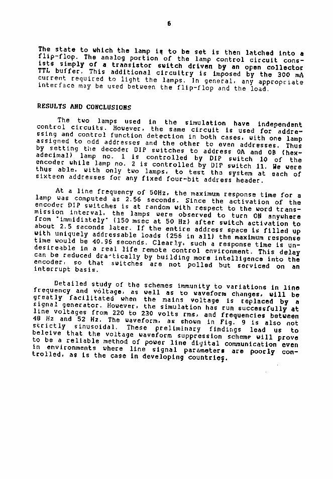

7
REFERENCES
1 ELBEL W Events in the History of Ripple Control Landis
and Cyr Reieu no 4 Zug Switzerland PP 3-18
and C Stillhavd Ripple2 J Van Heek Z Stanley Stys a proven load management tool Paper presented to
Control (Chicago IL Apr 20-22 1976)the American Power Conf
3 E Baumann DECABIT a new electronic Zellweger ripple
control system As reprinted from Zellueger Impulses No 3
Uster Switzerland 1971 Zellweger Uster Ltd
4 PA Schieper Bi-directional ripple control system the IEEE Control of
DECABITRETROBIT Paper presented at
Systems Conference and Exposition Oklahoma City OK
Power Mar 10-12 1976
5 Computerized ripple control eliminates execessive drain on pp 55-59 Mar 1977
electric utility supply Comput Des
PLS-1733 Technical Brochure 6 Plessey Rythmatic Control Published by Plessey (New Zealand) Limited
Box 21-142 Auckshy
land New Zealand June 1975
7 R Kniel and J Biro Low frequency ripple control systems 1 and 2 Zellweger
As Reprinted from Zellueger impulses Nos
Uster Ltd Uster Switzerland
8 Stonehouse BH and Waston PJ Load Control Signalling b7 Proceedings of
Distortion of the System Voltage Wave Form
the IEE 2nd International Conference on Metering Apparatus and
Tarrifs for Electricity Supply Sept 26-29 1972 pp 317-322
and Takuldar SN Electrical load management9 Morgan MG
Some Technical Economic Regulatory and Social Issues 2 Feb 1979 pp 241shyno
Proceedings of the IEEE vol 67
313
10 S Yunkap Kuankam Principles of a Digital Communication
Scheme Using Power Signal Waveform Modification Tech and
Dev Vol 1 No 1 Dec 1985
PARAMETER BOUNDS FOR A NE DIGITAL POWER LINECOMMUNICATION TECHNIQUE USING WAVEFORM MODIFICATION
by S Yunkap Kivankam N Ntomambr uago John ItBilikha
and DT Ngun Automation and Control lrihratory
Ecole Nationale Superieuri l-ilechique University of Yatoiri
YAOUNDE Cameroon
ABSTRACT
Suppression time tallis a crticaJ par1n-r in a new technology fordigilsi information transmission on electrical i r linesbab- on aignal suppressiur or nolsurppJreV8sit during a well deltor period bee inoingwith eachtrrorossing It affects the noise inimunity i~ii etectability)of the teclllolugv anid power signal distortion (aprerlhrg ittie power density spectrunt) inopposite ways ie tau values whith rinmuto improve noise immu jnty tend to worsen signal distortionand vier ers
This paper presents the results of w-m k -irried out on determiningbounds for tali Spetral analysis of the rn-iud power signal performedfor various values of tau shows that spectrA 1t-rtion varies proportionashytely with tal Signal detectability at a ftiutu of tau was determinedtheoreticaliy by asillning a given detector la aniupling window followed by a natch filter) The relationship is nonlmtr In conclusion acceptablebound for tali are -hown to be 11 ms and 3 m
INTRODUCTION
The physics -fa technology for informationmintI tranamiasgonon electrical power lines using power sigui neform modification wdaoutlined by kwankarn [I A low tension -nlation of thistechnoloywas attempted by Kedi [] and finally realized lIN Etoung andmNyemek (3]as well as Kwankam et al [41 Tihe method j Im-ud on sigfnal suppressionduring a well defined interval beginning witt rdItzero-cr aing This supshypression time tau is thus a critical paramett-r in the success nif the methodIn particular it affects the noise immunity (rinformation detectability)of the technology and power signal distorln-r (spreading of the powerdensity spectrum iii opposite ways Ie tan loeswhich tend to improvenoise immunity tend to worsen power signal lhtmirtion and vice-versa This pjaper lprebentthe results of work carried out imdetermining hounds for tau
hlt tseut Sm bfen atrted OUt fr grant tnntrwE tagtr Agency Ca lttsne Iretloprsnt(USA ID) nlusa itsProgam- to ens51- Jtaoop Co-ttoion (flST) AID P1010C -0 Y36-542 popml no 5204
Techa De VoL JVoI Junt 1987
34 Sa YAP sk m EosaudxforPowd LineConmwwArgjions 35
PHYSICS OF WAVEFORM MODIFICATION The modulating sigiJ is
Vaveform modification by signal suppression mNiy be considered asthe addition of a 180 phase diifted version of the signal during tie sp-preasion interval It may also be viewed as the limiting ae of amplitudemodulation ie 100 modulation Consider the wavrns involved in a single suppression as howin in Fig 1The unrcdifirt signal of radian frequency wo period Tand amplitude A0 i3
f(t) = losin(triIU(t) + A c n4 o (f-TI2)u(I _ T 2) (i)
where u(t)is the unit step functionwt twhere
tal Time
(b) Time
( ) Time
Fig 1 Signal Suppression during a Single Ilalf Cycle (a) Unmodified SignalJb) Modulating Signal (c) Modified Signal
Taet ampD Vol jNo I Jun1987
f2 (1) = Aosin(wot)u t) + Asin(cjot)u(t- ) (2)
where r is the suppression time
The modified signal is therefore f 3 (t) = f (t) +f2 (t)
= AsJin(Co 0 )u (t- ) + 10sin(Wo (t-T) )U (t-7) (3)
It is readily shown [I) that the Laplace= transform of f(t) in the casshyfor simplicity we have set A 1is o )o e sTF (s)
sw + - ]+2 cosw0jos ia (4)
As the power density spectrum of f3 t) is Fs (s) F3 () where Fs(sIis the complex conjugate of F3 (s) (4) also provides a way of determniniigthe effect of the suppression on the signal in terms of harmonica
Since the signal will be born-- by a power line it is important to camine te effect of the transmission line on the modified waveform Usingeither an L- r- or T bection as a model of a transmission line itcanbc shown that as a wave propagates along the z-duection its amplitudshyis given by
AoA( J[e-(z--X) + Pe(z-X)5)
+ e--X
where A0 is the amplitude at x = 0 )is the length of the line r is
the propagation constant and p is the reflection coefficientall given by well known expressiona Characteristic values for the linesencountered in Cameroon are shownin Table 1 The case of the low tensii line is not considered because of the
short transmission distances involved at this voltage level it is also assumedthat characteristic conductance is negligibly small hidetermining the effect6f the transmiuion line on fjit) it suffices to examine how f (t) andhf (tiare affected And given that we are simply interested in distinguishingbetween two states (0 and 1)in this scheme the influence of the fne maybe summaried in the losses suffered by an unmodified sinusoid We tallreturn to thiswhen we consider information detectability
Taec d DowVotiNo I JsE 1987
37 36 a Yap X Aget
Tye owhich Type of line R (Ohmln) L(Hkm) C~iFkin)
Single-phase 315000 and 175W V 083 005 654 x 10shy
Three-phase 02515000 V 030 157x 10 -
Three-phae 30000 V 019 066 0t02
Three-phase 90000 V 86 x 10-2 074 002
Three-phase 225000 V 49x 10-2 062 19 x 10-
Table 1 Characteristics Values for Lines in Cameroon
POWER SIGNAL DISTORTION
Since the teLhnology under investigations involves changing some characteristics of the power line signal quantitative knowledge of these
changes is indispensible to an evahation of the technology In attempting to determine a measure or set of measures with which such changes may be specified one readily thinks of such attributes as amplitude frequency waveshape harmonic content and the extent of discontinuities in the signal This last criterion is important to devices such as thyristors which are sensitive to rate effects anode-to-cathode voltage change rates in excess of hundreds of volta per mircosecond will cause the device to turn on
The switching circuits used and the voltages they are expected to switch in the implementation of this technology are such that there is no threat of hazards to deviczs which arc sensitive to rate effects Signal supshypression clearly does not affect the fundamental frequency of the power signal Similarly peak amplitude is only compromized if the suppression time exceeds one-fourth of the period Harmonic content while providing significant information on the effect of suppresion is inappropriate because only discrete frequencies are considered
A meare which appropriately defines the extent of the changes in the r wr signal is its power density spectrum (PDS) This is readily obtained rom (4) as a function of T By examining the changes in the PDS due to
wppmsmon we can readily see how much power has been introduced at any frequency or frequency interval of interest The PDS alto allows us
T ampD VoL3No I J~ 197
PwP mrctr Bommdsf or Po-r LJu CommsAcnus4n
to examine the effect of non-repetitive modifications to the power signal would not manifest themselves as increases in harmonic content
but rather as a change within a band of frequencies A clasaic example of
this is the difference in the frequClLy spectra of an infinite sinusoid and that of a semi infinite sinusoid Whereas all the power of the former i limited to one frequency (its PDS i an impulse) the PIDS of the latter i
spread out about its fundamental frequency Thisspreading in the ape
truni is the result of the single event of having turned on the sinusoidal generator at some instant or alternatively of having continuously sup pressed the signal before then
In order to determine the PIS of the power signal when a apecifi
bit pattern is transmitted observed that (4) may be written as
F3(s) =Cots) + GIs) (6)
where G (s) is the second term on the right-hand-side of (4) For an infinite binary sequence with ls iii bit positions k i k= have [ I
F(S) G5 1()1-4exp(-sx o) 4 exp(-2wsw +
+ G (s) lexp(- sk irw) + exp(-sk2 XIwo) + bull Jo
2 + + G( (s) lexp(sktrwso) + exp(-skl 7rt) + 1 (7t
Since transmission of a I) does nothing to the power signal a sequence t1 all Is is intuitively one which produces the worst case distortion For this case if is shown [I that
F3+ W + + W +
r shy2 (1 - co(2r w 0 ) )
cos(2rwwo)- I + j((jlu wiw0o) 2ini-rwwo)
[w0 - tocOslwo )cos(w I - csin~ i isinti)
-jsin(c o0 )cosit - wo cosi o0 )sin(wi (8o
Ttch A Dw Vol 3 No I ju 198 7
38ps Earsn eter Boundsor Ponr Lois CammuwI 91(
a U0t
TAU 0mg TAU= 18me
TAU 3 0m) TAU 36 me
Fig 3 abc u wcr Sinal pecri wi 1 au a a Pararctr
Tck d Dn Vol JNo I 1umiVS7 TechA DL ol I No I un7
40 S Yua Xankam rt Paeatet BOundsfo Potw line Communcaion 4 1
Curves for the magnitude of f(j w) as a function nf w with r as aparameter show that the spreading of the PDS of the power signal increases Observe that ss cxncted the unmodified power signal exhibit aspreading of itswith r [l] This PDS sbt SOllz the nominal line frequency Note twas verified experimentally using an hIPModel 3580A that the peak doesspectrum analyzer Suppression bme was viiried
not occur at prrci-vel 5UHz Two effects jointly accoontusing the circuit shown for this spread variation in line frequency and the departure of the wavein Fig 2 The reslts obtained are shown in Fig 3 The horizontal scale in shape from a strict sinusi(d (see 4) Snce the spectrum analyzer hathe pictures is 50Hz per a responds to 0Hz The
major division and the left most vertical line cor- well-defined sampling time the non-infite nature of the signal is of neghivertical ais is calibrated in decibels (dB) with each gible effect Note also the presence of a third harmonic in the mains signalmajor division representing 10 dB and with -100 dllat the bottomscreen of theAside from the firsi each picture shows two tracea with one cor- 6At T = 1 ms the major discernible change is the appearance of fifthresponding to the unmodified power signal seventh and ninth harmonics IHowever their totalenergy content is 1911of that of the fundamental As r increases the power content of the fundimental decreases while that of the harmonics increases At T = 5 2
mthe pcwer in the fundamental is down by 328 while that of the thirdharmonic is up by 4133 Note however that = 5-Ims correspoIuto suppression of better that one half of each half wave A suppreasintime of 3nis results in a decrease of oldy 108 in the power content of the fundamental
te) TAU 47g TAU L2 msw
Fig 3 e f Power Signal Specarum with Tau as a Parameter
rig 4 Unmodified PowertAne Voltage Wavaform
INFORMATION DETECTABILITY
Information detectabilitv as a function of r was determined theortically by assuming a given detector The detector is a match filter Onshysample of the line voltage appropriately aledaid full-wave rectified taken and compared to a threshold value The anupling instant is set so thaiit falls within the wopprrsoii interr l At this inslant a TTI Ditype flipflop whose data input is the procerd line vottage isclocked The outptilof the flip-flop is verted to ubtain the transmitted informtion bit
sdTo D VoLiNo I JuneJ987 Tech 4 D Vol 3No I JuneIV8
42 1 Y p wtcm asmetMe Budzfwr Po-w Ib CommskAftkoa 43
We Asume that only losses can occur on the transmibsion line Although Fig 5 The relationship is non-linear eventually saturating at 1 - 5mthis is true it does not necessarily mean that the voltage amplitude is mono- The phenomenon however is characteristic of the technology regardless of tone dercreasing with distance However if we further assume that reflec the specifics of the implementationtions are negligible then the influence of the line on the encoded inforshymation is determined strictly by the losses encountered by f (t) abovetLet be the threshold voltage of the match filter and o(t lt ) theo DETECTABILITY ()I COHESIVENESS (S) Y sampling instant Time is measured from the instant of the most recent zero-crossing of the corresponding unmodified signal The information is C a guetectable at a distance a from the encoder if and only if
to gt I sin ( ) (9)
W~o Aoeaz
where o is the attenuation constant to as given by (9) is the minimum acceptable value for
Type of liue Maximum length Minimum Percentage ofof line value of energy dissipated
Single-phase 17000 and 15000 V 80km 13ms 14
Three-phase15000 V 150km l3ms 14
30000 V 150km 13ms I15l
Three-phase m 90000 V 600km 09ms 05
Three-phase 225000 V 800km 09ms 05
Table 2 Minimum Suppression Time of High Tension Lines in Camroon
(for a Specific Oetector)
Using the values given in Table 1 to compute a we obtain the minishymum values shown in Table 2 for various types of lines in Cameroon The column at the right gives the percentage of the total power dissipatedby suppression if an infinite sequence of Is were to he transmitted with the corresponding value of At the values of - rnm bhown information detectability is marginal in that ny additional loss no matter how small will redilt in an encoded 0 being incorrectly decoded l improve on this must be increased The detectability of an encoded t) in the case of a loade line varies with everything else remaining fixed as shown in
T h A D Vol J o I Jc 1987 Tek Di 19870 VoL JNo I J
CONCLUSIONS
Minimum accepted values for have been discussed above for mediumand high tension lines over distances as indicated in Table 2 Acceptablebounds for r in the case of a low tension line where duetances loses are negligible maybe determined to the short dishy
from Fig 5 If we chooseA criterion of 50 detectability (defined below) the minimum acceptable value of is llms Above this minimum value the optimal choice of rdepends on the relative importance attached to information detectabilityand spectral distortion In general we wish to maximize a joint performanceindex of the form
L = + ko (10) where k o repreacnta detectability and represents spectral coliesi-k0venes Information detectability is defined as the percentage change in thevoltage amplitude which will resilt in an erroneous decoding of a tranA-mitted 0 bie Spectral cohesiveness is defined as the percentageenergy contained in the fundamental of tie total
In (10) cz and 0 are coefficients such that
ot + aft =1k
From the data obtained in the low voltage simulation 4] (Fig 5 we ampaitcld choose r 2 oms
REFERENCES
1 Kwanksm S Yunkap rPrinepLes of a Digital Communication SchemeUsing Power Wavefon Modification Technology and Developshyment Vol 1 no 1 Dec 1985 pp 23-40
2 Kedi JP wContribution c la Teleconduite Yume nque de Reseaux dExploitaion Electriquel Final-year project report ENSP University of Yaounde June 1983
3 Etoung LH and Nyemeck NG elRdaliation dun Simubateur pourTrnmisiondlnformations Nurnriques sur Lignes ElectriquesFinalyear project report ENSP University of Yaounde June1985
4 Kwankam S Yunkap Ngundam IPI Ningo N Ntomambang andNgamy DT cLow Voltage Simulation of a New Digital Power Line Communication Technologyo ANSTI-EE 86 ElectricalEngineering Conference University of Dar es Salaam bar esSalamm Tanzania Aug 18-20 1986
TicA 5 OemIol j o I mzne1957
HYDRAULIC PARAMETERS OF HRU SOIL
by
SIA Ojo amp CA (ThotHydraulics tesearch Unit University of Lagos
ABSTRACT
This paper reports a case study of the determination of the soil hydrauic parameters for soito of the Ilydraulics Researchuurface Unit Universityconductivity of tle oil denoted by k Both laboratory and field teats wrc
cmployed in its determination
it waz foAnd from tile study that the hydraulic conductivity can be
rpresentd by the equation
= k(cde indicating the effect of the shape of tIhe particles c the grain size d and thevoid ratio e on the samples conductivity In this study the effective grainsizes ranged from 0009mm to 00015mm in diameter Using similar sampletubes of dimensions l00mm diameter by 127mm length hydraulic conducshytivity values varying from 52 x 10 mms to 11763 x 10-3 mms (for field teats) and 10 x 10 to 226 x 10 mms (for laboratory tests) were obtained
NOTATION
Unless otherwise stated the followipg underlisted symbols have the follow ig menings
A -Area (in) CD - Drag coefficient
11 -- Presare head (in)
NR Reynolds number Q - Water discharge (m 3
s)
Ss Specific gravity of soil particle Speci ty ooiac
V - INocityVe (mis)Teck 5 Lt Vat IfNa I wig 1987
PFROsGREss REFORT
ON
PROJECT N( 5204 DIGITAL INFORMATION TRANSMI SION0N LECTRIC POWER LINES
PREPARED BY
PROF S YUNKAP KWANKAM
AUTOMAT ION AND CONTROL LABORTORY
Ecole Hatioual Superinue PolytochnioueIP 8390 YA0ND Cauroon (237) 32-12-26Te|I Tele 8384 KN
April 1987
Recd in Sc NOV 4 t9p
INTRODUCTION
The project document was signed on June 28 1985According to this document progress reports were to havebeen submitted within thirty days of the following dates December 31 le8s June 30 1986 and December 31 1586 This has not been done for the reasons given below
The PERT chart in the work plan indicates times withrespect to the date of availability of the neccessaryequipment The first batch of project equipment purchasedin the US in AugustSeptember 1969 was delivered onDecember 24 1985 There were also some delays in gettingthe space allocated to the project prepared for installation of the equipment The result of all this was that theexperimental aspects of the project did not begin untilFebruary 1986 The first
written in format by
March 1986 and represented report was results some
therof
efore written which
in were
already obtained but mostly anticipated
In the absence of any guidelines the report was a summary the Principal Investigator
(PI) The PI also indicated in his covering letter -thatshould the format be found inadequate he would redo thereport according to the guidelines provided Fred JBieganskis letter of February 12 1987 to the PI is the first official reaction to the report
PROGRESS MADE IN WORK PLAN
Before undertaking a hardware simulation of theproposed technology at nominal power line voltages and currents it was deemed necessary to carry out a lowvolatage simulation The advantage offered by a low-voltagesimulation was that the encoder and decoder systems could bemastered without delving into problems posed by operation atthe nominal values since these systems remain essentiallyunchaged even at high voltages and currents
A low-voltage simulation was realized and used to testthe physics of the scheme Details of the simulation appearin the paper entitled Low Uoltage Simulation of a NewDigital Power Line Communication Technololgy see Appendix 1
The next step was to implement the encoder and decoder systems using microprocessors as opposed to the discretelogic circuits of the low-voltage simulation These sstems are now implemeted using the Motorola MEK6802DS single-boardmicrocomputer This has enabled easy modification of systemparameters such as suppression time and the study of theireffect on detectability and spectral distortion The results
2
obtained for the low-voltage simulation which appear in the paper entitled Parameter Bounds for a New Power LineCommunication Technique Using Waveform Modification(Appendix 2) have also been obtained at the nominal line voltage of 220 volts
The lcw voitage simulation exploited the voltagesuppression scheme in the control mode ie loads werecontrolled remotely from a given point With themicroprocessor implementation a data transfer and aspectrum analysis mode have been added In addition aninterface for the MEK68O2DS has been ralized which permitsblocks of data to be transferred from a microcomputer withsecondary storage through the parallel printer port intothe MEK6BO2D5 for serialization and transmission A paperbased on the abstract shown in Appendix 3 is in preparation
The interface between the encoder and the power line isthe injection circuit This is what causes suppression ofthe line voltage for a Fixed time beginning with the zerocrossing when a binary 1 is transmitted Three types ofinjection circuits have been examined but only one indetail as indicated in the paper entitled Injection Methodsin a Digital Communication Scheme Using Power SignalWaveForm Modification see Appendix I We have fixed onparallel injection Two configurations are possibleparallel injection with a series pass element and parallelinjection with a shunt element Currently only the series pass element configuration has been implemented
In terms of the work plan these results represent theaccomplishment of only items 1 2 3 S and 6 of Phase 1 ofthe project However from what we now know they representbetter than one half of the effort and time required toaccomplish all the objectives of the project contrary towhat is indicated in the PERT chart Phase 2 workexample simply
for depends on the presence of a reflected waveand the detection of positive and negative peaks as opposed
to positive- and negative-going zero-crossings Theimplementation of the encoder and decoder using single-boardmicrocomputers should reduce Phase 3 work to primarily that of assembler language programming A revised schedule is shown below
EXPENDITURE
Out of a total budget of One hundred thirteen thousandFive hundred forty-four dollars ($113S54) a total of aboutFortg-two thousand seven hundred seventy-six dollars($42776) has been spent The expenditure breakdown is as follows
- Equipment - $31129
- Technician salaries - $ 3192
- Overhead - $ 2455
OCFA expenses have been converted to US dollars at 350 F$
OUTPUT SO FAR
The following qLint4fiable outputs have been obtained so Far From the project
3 papers presented at ANSTI-EE 86 International Electrical Engineering Conference Dar es SalaamTanzania Aug 18-20 1986 and one abstract(The paper on parameter bounds will also appear inUol 3 no 1 of the journal Technologa and Development)
- a low-voltage simulation oF the technology
- a 220-volt implementation of the technology for unidirectional communication from generator to load
UnquantiFiable outputs include a significant amount ofinstitution strengthening The facilities provided throughthe project are the main equipment support of the Automationand Control Laboratory (ACL) of the Ecole NationaleSuperieure Polytechnique (School of Engineering) of theUniversity of Yaounde The ACL currently numbers ten Fullshytime faculty members of the Electrical EngineeringDepartment and two associated researchers From outside thePolytechnique The ten faculty members represent two thirdsof the Electrical Engineering Faculty and one sixth of thetotal Polytechnique academic staff Most of the output ofthe ACL (see enclosed brochure) is directly or indirectlyrelated to the facilities provided through the projectThese outputs have in turn attracted other grants andactivities to the Laboratory
DIFFICULTIES ENCOUNTERED
We have encountered two types of difficulties onetechnical and the other logistic The technical difficulties have to do with tha supply of equipment and components
The unavailability of certain electronic components inCameroon has caused long delays in the project Inelectronics work one cannot determine in advance all the types of components that will be required on a project Thepossibility of easily picking up components as the needarises must therefore exist if the project is not to besubjected to severe delays This is not the case in Yaounde
4
Some components have had to be ordered from the US Andbecause the quantities are very small the orders are not ofcommercial interest to most suppliers Those isolatedsuppliers who are willing to handle such small orders are inno big hurry to Fill them either The project has thereforesuFferred severe delays par-ticularly as concerns therealizazicn of the injection ciucuits Technical details onthese difficulties are given in Appendix 5
The second type of difficulty encountered is logisticalsupport primarily transportation Lengthy arguments wereadvanced in October 138S as to why a transportationcomponent should be included in the supplemental budget (seaAppendix 6 For excerpt) This aspect of the request was notapproved Those items which have been purchased locally havetherefore necessitated the absence of some member of theresearch team every time a purchase is made And given theimpcssibility of calling in advance to determineavailability some outings have been tours of the city
In addition to this expenditure in time justifiableexpenses have been incurred which unfortunately cannot bedocumented in a manner acceptable For reimbursementCameroonian taxi drivers and bus drivers do not givereceipts And when the Pls personal vehicle is used thereis no way of documenting this other than by odometerreadings It is not clear if and how these readingstranslate into project dollars So claimsno have beenmade Finally receipts From purchase of gasoline areinappropriate since the vehicle is not used exclusively For project activities
MODIFIED WORK PLAN
The work plan is essenitially unchanged What haschanged is the schedule The modified schedule is as shown in the PERT chart attached
CONCLUSION
The scientifique basis for the proposed technology issound We therefore cnntinue to hold high hopes For thisproject despite the difficulties we have encountered Theseall stem from working with Fairly sophisticated devices in an environment which lacks the support system - in this caseprimary and secondary sources For components - on whichadvanced teci-nologically must rely
5
April 1967
0 Time in months
PHASE I
1
2
3
REVISED ACTIVITIES SCHEDULE
3 6 9 12 15
S
PHASE II
2
3
PHASE III
A MULTILEVEL MULTIPROCESSOR SYSTEM FOR AUTOMATIC DATA
LOGGING IN A NEW DIGITAL POWER LINE COMMUNICATION SCHEME
by
S Yunkap Kwankam N Ntomambang Ningo and F Nematchous Automation and Control Laboratory
Ecole Nationale Supgrieure Polytechnique University of Yaound6
SUMMARY
The robustness of a technique for transmitting digitalinformation on electric power lines using waveForm modification first suggested by Kwankam Ei] and implementedby Kwankam et al C23 is tested by measuring its immunity tovoltage amplitude variations frequency fluctuations andvoltage waveForm changes As -transmission rate is only 100bits per second (limited theby number of zero-crossings per second) a system For unattended transmission reception
errorand automatic logging becomes imperative if statistically significant amounts of data are to be logged
The system is a multilevel multiprocessor data loggerText resident in a File in a microcomputer C an ATampT PC6300) is down-loaded 8 K butes (characters) at a time to aMotorola EK68O20S single-board microcompuLer The 6802board then introduces parity and other bits appropriate tothe protocol used and transmits the characters out on a power line Transmission is bit-serial At receivingtheend a receiver-decoder implemented on another Motorola MEK680205 recovers the individual bits checks for anyerrors and assembles them into characters The assembledcharacters are then uploaded again 8 K bytes at a timm toanother ATampT PC 6300 microcomputer The microcomputer in turn saves the received text in another disk file
On downloading communication between the PC 6300 andthe 6802 is through the parallel printer port of the former and the peripheral interface adapter (PIA) of the latterThus a data transfer rate of 50000 bits per second (limitedby the 4-MHz clock of the 6802) is readilW acheived withoutadditional hardware This is significantlU higher thanhigher than the 9600 baud available through the use of theserial port and thus frees up the the PC 6300 to performmany other tasks in between servicing the 6802 on an interrupt basis
Uploading is done by means o an interface usingminimal hardware which occupies one of the slots on thesecond PC 6300 and the IN instruction in an assemblerlanguage code The control programs in both PC 6300s arewritten in BASIC Data transfer rate on uploading is about20000 bits per secono
The system is capable of logging date continouslUuntil the source disk is empty (and the destination disk isfull) For Floppy disk files this takes about 10 hrswhereas For Files on 10MB hard disk systems data transfer can go on for 275 hours non-stop Using this system therobustness of the communication technology has beenthoroughly tested with minimum human intervention Itsadaptation to other environments where unattended logging is unavoidable is straight-forward
data
2
APPENDIX 5
Parallel injection with a series pass element meansthat the load current Flows through the switching device inthis case a thuristor The thgristor is Fired at the zeroshycrossing to transmit a 0 or is Fired aFter a delaycorresponding to the suppression time to transmit a 1 Inthe latter case the voltage waveform is therefore suppressed as required by the theory However the currentFlowing through the line depends on the nature of the loadSpecifically when the load is resistive the thyristorcurrent goes to zero at the voltage zero Thus the voltagewaveform at any point downstream of the point oF injectionshows suppression beginning at the zero-crossing If thetotal load is not resistive there is a phase shift betweenvoltage and current The thyristor current does not go to zero at zero voltage but some time before or thereafteraccordingly as the load is capacitive or inductive In our case the load is inductive Uoltage suppression therefore starts some time after the zero-crossing the more inductive the load the later this occurs
Suppression can be returned to the zero-crossing byphase compensation A capacitive isload connected inparallel with the inductive load The capacitive load ischosen so that It resonates with the inductive load at the line frequency 50 Hz in this case The small inductancevalues oF the load when a transformer is used to tap of themodified signal for detection purposes require unmanageablecapacitance values ( around 1 F) To reduce this toobtainable values transFormer-coupled capacitancecompensation has been employed A second transformer hasbeen used whose net effect is to multiply the capacitance- as seen From the primary side (the line) - oF thecapacitor connected across its secondary This has worked quite well in terms oF reducing the displacement oF thesuppression from the zero-crossing However minor problemsstill exist beacuse the suppressed portion of the signal isnot Flat (zero) This simply translates to a more elaborate detection algorithm in the microprocessor-implemented decoder
All oF this could be avoided by using a shunt elementconfiguration in the parallel injection circuit This can bedone with either h gate turn-off (GTO) device or atransistor Use oF a thyristor would imply Forcedcommutation and therefore voltage suppression would not betotal We have not been able to Find either a GTO device or a high-volatage swithching transistor (which does not have aFree-wheeling collector-emitter diode) Welocally havetherefore had to order these And given the insignificanttotal dollar value oF tie purchase we have the delaysindicated above
INJECTION METHODS IN A D(TAL CO(M-IJNCATIGN SCHEME USiNG POWER
SIGNAL WAVEFOHM MODIFICATION
by
S Yunkap Kwankam JM Ngundam S Tchouate F Nematchoua E Ondoua and Awono Onana
Automation and Control Laboratory Ecole Nationale Supericure Polytechnique
University of Yaounde YAOUNDE Cameroon
This research has been carried out under a grant from the UnitedStates Agency for Internaational Development (USAID) under itsProgram for Science and Technology Cooperation (PSTC) AID project no 936-5542 proposal no 5204
Abstract
This paper presents the results of investigations into threemethods of achieving power line signal suppression in adialtal communication scheme
new which uses power signal waveform
modification The methods are (1) series injection throughmutual induction of a 180-degree phase-shifted version of themains (2) series injection by use of a third winding on a transshyformer as the control input and (3) parallel injection by use ofboth shunt and series pass semiconductor switching elements Ineach case the efficiency of the method is measured as the amount of suppression for a given modulating signal of known power
Parallel injection using either thyristors or transistors isshown to be far more efficient than the series injection methods
3
INTRODUCTION
In a new digital communication scheme advanced by Kwankamand others (1-3] the poer signal waveform is modified to encode 7 n o ss n s s -s rr re i- -a
reports on the experimental investigations of three methods ofachieving signal suppression In each case the efficiency of themethod is measured as the amount of control signal power requiredto suppress a given power line signal for a fixed duration
SERIES INJECTION
Consider two electromaanetically coupled circuits as shownin fig 1 [4] We are interested in the conditions under whichthere is a net transfer of energy from one circuit to another It can be shown that for currents i and iwith a variable phaseanale difference one circuit will provf-e more energy to theother than it receives from it for some value of the phase angledifference The currents are
1i = 11 eJ(wt + 91) (1)
T2 = 12 ei(wt + e2) (2)
The complex powec due to the coupling is 9Irl= = 12 eJ ( 2 - (3)i )wM I2 81)
= = 2 jWMIlI 2eJ - )2) (4)
where
means complex con)ugate
(3) and (4) may be written as
31 = wM 2 11 sin(0 2-81) + jwMI 2I 1 cos(e 2-e9) (5) =S2 wM211 sin(8 2-el) + jwMI 211 CoS(E 2-91 ) (6)
learly 31 = -S2
Active and reactive power are given by
P = -P2 = WM211 sn(82-eI )
for active power and
81 = 02 = wMI2 11 cos(9 2 -31 )
for reactive power
Fig I Two electromagnetically coupled cLrcuts
C
Fig 3 Phase shift regulation circuit
~ UA I
r II6
u
Time
t
(a)
iI 1 A -
E
(b)
Fig 2 Instantaneous circuit variables for
(a) power line (b) injecting circuit
4
Depending on the time interval considered energy transfer
could be positive or negative Positive power transfer means that
there is a net transfer of energy from the source considered
h e ne7 r- erns 3 net t ansfer of enerqy to the source
If 91- ( lt 0 then P1 gtO and P2 lt0 Therefore the first
circuit is tranfering power to the second circuit On the other
hand if n_ 10 then P20O and P (0 The roles of the circuits are then regersed Now suppose that the firsit circuit is a power
line and the second is a circuit injecting energy into the power
line Then we have
= 71 sin wtV0
72 = -V1 sinwt = - V1 sin(wt + ()
i2 - I2 eJ(wt + i + 02)
For the injection circuit to transfer power to the line we must
have
gt 8 2 + 81 gt 0
Maximum power transfer therefore occurs when 82 = Tr2 - 81 Generally in a well regulated system the power factor is of the
order of 08 with a value of -n6 for 81
Figure 2 shows the instantaneous power P1 of the power line and the power P2 of the injecting circuit Notice that P1 is negshyative and is positive at the moment of signal suppressionP2
A circuit which may be used to provide phase shift regulation is shown in Fig 3
The coupling betueen the circuits of Fig 1 is limited by the fact of the flux linking them having to pass through air a
low pemeability medium In a bid to decrease the losses in the
flux linkage between the circuits we conceived a three-winding transformer showm in Fig 4
THREE WINOING TRANSFORMER
We have a magnetic circuit on which there are three separate winshydings
a primary winding with n turns
a secondary winding with turns andn2
a tertiary winding with nc turns
SC
v()Wn VC o- -- -- 4
_
4-
Fg 4 Three-winding transformer for n)ection control
5
The primary and tertiary windings are wound in oppositedirections with = nl When Snc is open the system operates as an ordinary two winding-transformer Let us examine this case in more det i
V1 (t) =Vim cos wt (9)
In the magnetic circuit we have
V1 = -el = n-dG (10)
dt
where
60 is the open circuit value of the flux and is given by
Vlm = - cos(wt-ff2)6 O (11)
n1w
We notice therefore that at constant frequency the flux dependsonly on the voltage
At the terminal of the secondary winding we have
d6o V2 = 12 = -n shy (12)
dt
When the switch S is closed we have
V1 = jLiwIl + jMw1 2 (13)
V 2 = -jL2 wI2 - jMeI1 (14)
n1ll + n2 12 = nII1 0 (15)
At open circuit (i =0) with switch S closed a fluxsecond opposite to the firs is produced as a result of current flow in the tertiary winding Thus
Vim Vim 1 - 1= - cos(wt-r2) = - cos(wt-ff2+ff)niw u
Vim -i cos(wt+ff2) (16)nim
The resultant flux in the magnetic circuit is theoretically zero
V
D
D 7406
RL = 2 7-a 5 W
D = IN5341B
R8 = 12 -a
Rc = 330JI
R = 10O-Q T = (Schc ffner) IT 313
Fig 5 Control circuit for parallel injection
7
RESULTS AND CONCLUSIONS
We m~y define the inefficiency n of a particular in)ectionmethod as the amount of injected power required to suppress agiven amount of line power as a percentage of the latter The results obtained show that the parallel injection methods are theleast inefficient while the series methods are the most wastefulThe computations show that the series injection method requiresat least as much power to be injected as that which is to besuppressed not counting losses In the three winding transshyformer these losses are such that when the inputs to the twoprimaries exceed 120V it requires an additional lOZ of the powersignal to obtain total suppression On the contrary the injected power in the case of the parallel methods may be considered asthe total dc power dissipated by the circuits driving the gatein the case of an SCR or base in the case of a transistor This was measured to be around 18W The line voltage suppressed was 220V rms Assuming a minimum load current of 1OA and thatsuppression time is a line2 msec on 50Hz we find that the inshyefficiency is a scant 8
REFERENCES
1 Kwankam S Yunkap Principles of a Digital Communication Scheme Using Power Signal Waveform Modification Technologyand Development Vol 1 no 1 Dec 1985 pp 23-40
2 Kwankam S Yunkap Ngundam JM Ningo NN and NgamyDT Low Voltage Simulation of a New Digital Power Line Communication Technology ANSTI-EE 86 Electrical EngineeringConference University of Dar es Salaam Dar es Salaam Tanzania August 18-20 1986
3 Kwankam S Yunkap Ningo NM Bilikha JB and NgamyDT Parameter Bounds for a New Digital Power Line Communishycation Technique Using Waveform Modification ANSTI-EE 86Electrical Engineering Conference University of Dar es Salaam Dar es Salaam Tanzania Aug 18-20 1986
4 Etoung LH and Nyemaeck N Realisation dun Simulateur pourTransmission dInformations Numeriques sur Lignes Elecshytriques final-year project report ENSP University ofYaounde June 1985
5 Mak ST and Moore TG Jr TWACS a New Viable Two-WayAutomatic Communication System for Distribution NetworksI Inbound CommunicatLon paper 84 WM 182-2
Part IEEE Power
Engineering Society Winter Meeting Dallas TX Jan 29 -Feb 3 1984
6 Mak ST A new Method of Generating TWACS Type OutboundSignals for Communication on Power Distribution Networks paper 84 WM 181-4 IEEE Power Engineering Society Winter Meeting Dallas TX Jan 29 - Feb 3 1984
PROJECT N 520 DIGITAL INFORMATION TRANSMISSION ON
-E CTRICAL POWER LINES
PROGRESS REPORT March 4 1986
This report covers progress made on the project since the grant documant was signed on June 28th 1985
Purchase of equipment
The prinpipal investigator took advantage of his visit to the US as a ibright Visiting Scholar during the summer of 19SB to purchase most of the basic equipmentneeded by the project These included the computer systemsthe spectrum analyzer and sufficient components to completethe low voltage simulation of phase 1 of the proposal
Experimental Work
A hardware implementation of the technology on a low voltage (30-volt) line has been completed Two lampsconnected to the same 30-volt source are independently controlled by two switches using the technique
Work continues on various injection methods where parallel injection using a pass thyristor seems to be the most promising
Publications
One paper (see appendix 1) has been published on the principles of the technology Four other manuscripts are in preparation for the ANSTI EE 86 Electrical Engineering-conference scheduled for August 1986 in Dau es Salaam (see appendix 2)
Supplemental Budget
A supplemental budget of Sq6350 was requested in October 19BS Of this amount S2SOO was recommended For approval Further purchase of equipment awaits final approval of this budget supplement
Recd in SC NOV 4 1988
0
~1II
UU
rUL
LW
4
c
-
~~t
~aoJ
a ~
~ u
tAshy
44C
4
U
2
0
N8 CL-
CF
i4
1-~ 0
-
--
I --
0 C
-)
LQ
~
24
25
S Y Kwani2n Nou~s aLons decrit en ddtail une methode on IVioninnattt htnare est ode ar lag
presence ou lab sence du signal de puissance r la gne pendant un tntr alle hie nd e i nt cvonmrneItanr iI chaque crosement a ziro Un code I en supprtmant lesignal et ) en tie lemodifiant pas
Les pnincipes de Vencodeur que nous arons ddcrtts unt lutlitIrate di usignal de puissance modifie dune aiiallsecodee ont ite egalement decritesen deads Les cnteres er les De uxnetjades de 3pec-Jde -tc) ie a eqiie ne binaire
che rtdes pamm etres de do n nes La different t relationrqut dteterfntnett Ict t ontn eleure tethodiepermettant
int de rn inniserla distortion ispectrale
a natdi et titla tnestgn ial uise sance
INTRODUCTION
The need for transmitting information on electrical power lineshas existed eversince the advent of electrical power distribution networks SlIIe control functions needto be exerctsed at various points in the network for load management fault Isolation andother purposes it is economically advantageous to use the wiles themsehesmunication link This idea was advanced as early as as the comshy
1898 by Routin and Brown I I
There are currently two basic approaches to exploiti g this idea T hietraditionalapproach in operation since the latecommunication systems f21 19 20s has been through the use of ripple controIn these systems narrow-batwfrequencies between ( 1-20 Hz) pulses with carrier100-1000 Hz arestations Tie
injected into the power lines at distribution subshysame principle of carrier-bome signal injection s used for voice commushynication between stations-on power networks [3]
More recently attempts have been made to develop communication technologiesDased on the use of the 50-or 60-Hz power signal as the earner Direct-aton schemes for digta communication include flattening of the waveformwaveform modii-Ftops 14rodmodulation of the location of the zero crossing [5] The latter scheme wasdeveloped)yArthur D Little Inc ofCambridge Massachusetts
THE YAOUNDE SCHEME
The scheme described in this paper is currently under investigationrationale Supirieure Polytechnique of the at the EcoleUniversity of Yaounde Here binary infor-iauon is encoded as the presence or absence of the power signal oathe line during a
Tch J Dev Vol 1NoI lec IY8J
I l ieI
wejl-hciiel itiicviilegonig tlih eChCI Lzeti tus~itg (ihl~ded by suppie siing ilhes g al an d t) y lc auig th e s glJau n moi d as show [g I
ca r e BIT
0
A 0at
d car ie
Fig 1Typical Wavefoms -the Ya centur IeSheme
Aside from thecoming of the ADL schemeneed for originality this researchModulation of the intivated hy a major shortshypredicated on the assumption zero sviesof thethat the line frequency is power signal istv ightly contrulled Ilhisishave shownnot tile casethat iine frequency varies between 48 and 52 Ii It)] in the local electrical environment in Caiclti Informal measurementsworkable The Yaounde scheme is
no matter what the line frequency variations acedent on the foi n Ili addition it is not depenshyof tie power signal as long as this stgia is strictly monotone aroundthe zero crossings
Tedh 1 Des Vool I ec1985
26 27
S Y Kwankam I) tug-jIPower Line (mnJ4
switch ht all lllvcrllli amplifier Fie zero crossing ainti p I A --ileand using
co m pai l r a re sei o ilia t th e a n a og switc h is Iu iO i- n s11holy t le and t u-ehr ne d oit slofrltv itter each zero crossing seeLOAD I of that of I Fig 5 The gaint lihe niplifit is the ieciprocalthe attentatOr lhus the signal at the output 1 he sinpidies when the switch
CONTROL FACILITY
LOAD N
RCS =Remote Control Switch Fig2 Model of system for the Yaounde Scheme
The scheme is designed for use in any electrical environment which can be modelledas shown in Fig 2 Examples include a low tension network served by a single substationa set of substations served by a single medium tension tr3nsmision line and the entirenetwork uf a micro- or mut-hydro facility Remote control switches (RCSs) I throughN are turned on and off to supply or cut-off power to various loads In the system current-ly under investigation each RCS is given an eight-bit identification code and each transshynsion conssts of 15 bits For a 50-1z line a single controller can thus access all 256RCSs in the system in 384 seconds
ICA
AA
ENCODING PRINCIPLE
To encode the binary intormation the zero crossings of the power signal are de-tected and the signal i left unaffected for a 0 or surpressed during r seconds for a ISignal suppression is hieved by adding to the signal a 180-degrec phase-shifted versionof itself A tinctionia block diagram for the encoder is shown in Fig 3 and furtherelaborated in Fig 4 The power signal is attenuated and then fed through an analog 14 l-shy
0O
I
Tech d De Vot 1No1 Dec 1985 Tech d Dev ampVJ 1NoI Dec 1985
28
19
S YKwankam
is oi is equal in magnitude but opposite in polarity to that at the input ) [lile attenuatorZero crossing detectors (ZCDs) are used to trigger monostable multivibrators such thatthe pulses at the output of gate OR I occtr within the onshown in Fig 5 le tine of the analog switch asamplifier output has-thereture stabilized before any signal injectionoccurs The pulses at OR I are ANDed with the bit to be transmitted D LJT to providethe control signal to the injection circuit Typical injection ircuits beng investigated appear in [2 7]
I
II
- Z If
D -1
J CL4DcK
I
ORt ljjJ 1i
Fig 5 Triming diagram for the encoder
It is assumed that the control program for the scheme is storedmemory for examole The - in computer15 bits which constitute each block of information are trans-ferred from storage into a buffer In the current simulation the buffer is accessed every150 milliseconds and theclock for this circuit istakenlaaa serialized by the circuit showii functionally in Fig 6 Thethe output of gate Al1of Fig 4
The encoder circuits have becn definedwith only minimal consideration for reducingthe hardware cost The emphasis has been on accurately encoding the binary input se-quence using the waveform modification scheme described By contrast cost reductionplays an important part in the design of the decoder This is justified by the considerationthat there can be as many as 256 decoders for each-encoder in the system
FREQUENCY SPECTRUM We now consider the frequency spectrum of the modified signal Let FO(s) and F (s)be the single-sided Laplace transforms of the waveforms associated with the transmission
Tech amp Dev Vol 1 No1 Dec 185
Ditil oer ne (ommun
of a single 0 hit and a single I bit respectively ie Fo(si i ifte transfujit of the positivehalf of a pure sine wave Then ie waveform associate itihthe transmission of the binary sequence 1 b transforms by the time delay iipelty toF(aj = plusmn [(b ( Om)lt s + (b (D I)Fo(s1 o
-b reg O)Fds exp( -rw 0o -(b C) )F(l ekxpt-rwo
0
+(b Q t)DFt() (p( -21lrw)
+(b (D I)Fo(s) expf -2asrw) + I 1where wQ is the frequency of the unmodified sinusoid and Q represents the logicalExclusive-OR operation The plus sign is selected if bo is iansnitted at a zero crossingof positive slope Othenvise the minus sign is chosen
It can be easily shown that for the carrier of(]) at1 at uming an amplitude of Ivolt and transmission at a zero crossing of positive slope
F5(s s2 + exp-xirWoJo (2J0
Tech ampDer Vol 1 No Dec 1985
+ 7
-~
~- ~
77
70
I L
7
a FT
RN
4
~~ 1 R
Vy 1F7
-44~
p-1
~154
~~IT
~_41
-+
~---2
~
h+ ~c
-le +
-+
LL
~ +
~ al
~pW
~~p
~
~ +
V
ttc
EO
0
P jN
~1-
C
a
-I LFi-
-1
~ 4
~
34 S Y Kwankam
a detector which does not operate on the demodulation principle
Two different methods of one-step detection of the binary sequence are currentlyunder investigation In the first method the modified sinusoid - or some fraction thereof - is rectified and sampled at somewhat follows time instant to during the suppression time (Intime is measured from the nearest zero crossing of the correspondingmodified sinusoid) This sample un-is then digitized by latching it into a flip-flop as either
a0 or a 1see Fig 9
0alt)DT DATA
LTCH
CK OUTPUT
COMPARATOR ONE WITH SO
IHYEIS SHOT
Fig 9 Scheme for one step detection of encoded bits
The corparator-with-hysteresis server as a detector (In actual operation an antici-pator) of the zero crossings The monostable multivibrator provides apling occurs delay so that samshypreci-ily at to The multiplier a as shown below is a nonlinear function ofvin This is because dtrinampsuppreaion time the sampled voltage for a transmitted 0 mustsansfy the input threshol conditions for the type of logic technology employed whilethe same signal must not exceed the maximum allowable input voltage at any time Thehardware is chosen such that a is a constant during suppression timeSuppose the flip-flop has the following characteristics and vv0 are the maximuminput voltage corresponding to a logic 0 and the minimum input voltage corresponding toa logic 1 rea ctively ts is the set-up time for data input and th is the hold time for datainput (after T clock transition) Then correct detection of the encoded bit requires that
(wint)gt Y1 fo-ts lt I lt to + th t7)
to is reated to r by the inequality
to + th lt r (8) If the corparator-withhyteresia Is simply a Schmitt trigger buffer of the same logic family w e-asohave
Z-champDe Vol 1NoI Dec 1985
bull
tl Poier line Common 35 15Vtnt) ro 0o lt I t
(9) where t s te time delav between the 1-to-0 t in of the output ot the bufferand tilenext zero crossing-
In(9)we have ued the symnetrN of the ectified sjjiout tie zero crossng when nh e e ed t s f t
Criteria for chosing C 7 toand t1
two importint criteriaIn ( 7) and lr the only parameters leftinvolved to our ctwicein tile choice otT We kho re a r t( and ti There are
(i) tinimnte pectral distoltion ard (ti) maximize the distinguishability of the signai responding to encoded 1ancorrespondig to an encoded 0
The choicechoice ishowever jgreatly ofinfluencedparamountby a Given awe of - thus importance to ire success ot the scheme Thisrmusthuose r such that
rint)I t =nf2w o (10
where vm is the maximum aiiowable input voltage for thLilc technology used
Taking the equality in (8) and substituting for to + th I asJ well as fbr vin in (7) and(10) we obtain
Q I i
Taking v = 25 volts vm 50 volts typical values for Il1 ntes and A= 220 volts the bounds in (lI deiiie an interval
choice l1T only if rgtrt6wo Th early violaies criterion (i)above for tile
This predicament is avoided by making ota nonlinrc minrction of v In paiticuIr (vin) as shown in Fig 10 where inmits the choice the nonlinear regio u ries inverSely with vii perof mrch smaller values fordistortion a functtotns of this type and thcreie 1re lfTrimiathon of spectr-lcan be readily realizcu ncrig commonly used circtitelements ithe present investigation ko 1
With (10) satsritpd and a I during suppression ti -mtntlie smallest allow able value
Tech amp Dei iol INo Dec IY85
C
36
37
S YKwonkam Digital Power line Communiati
a
0(
0
Vo SFig1i Juaa function
l1enak ltlt1
In e curve for fuuther miinizatln o spectral diutortion - ktgt
Fig 10 Phl u1Ivplpi a curve wilichmImozessp rili$1ukllolinearregiona varies iversely withVin)
4 d in non
for r is found by taking the equality in both (7)ant (8) This gives
Tmin = (lwe) sid (iVlA) + ts+ th (12) Choosing the equal sign in (8) clearly fixes the value of to And since a is now determinedti isread ound from (9) to be (1w 0 ) s nf (vdA)
It should be noted that the criteria indicated above do not invariably lead to theexpreWsions obtained for the various karameters rfor example can be greatly reducedby making tie parameterc ajump functon Of in
-As in Fig 11 a could be very large during sunpression time and very small or evenzero at other tunes Similarly the comparatoi-ith hysteresis could be made to approxishymate a zero crossing detector quite accurately by using the circuit shown schematicallyin Fig 12 in which t can be mad~e arbitrarily close to zero Thes refinement howeveronly add to the complexity of the detector Sini- every branch transmission line aadultimately very subscriber implies one such detector it is of great economic imnortanceto keep the aetec3r as simple as possible Reliability considerations also dictate that thedetection process oc uncomplicated
VR2
Vin
VRI
+ X0 Cc
MUX Y
+
Yiamp U Schrmc of cornoarstor with hyuieruis usedfor Zero The i-I transitionO Bc ico n t o cur ritrsi
-ng
KlL
i ilteinstion Mteo thsetrocros
Q
Tech amp Dev Vol NoI Dea 1985 Teds D Dev Vol lVo1Dec 1985
39
38M S Y Kwankam
DtgraPower Ui e Communication
AN ALTERNATE APPROACH Clearly a I can be detected without examining the output of the zero crossing detector A second method of T ieepdetection which is aiso under ivesigatun is a diffe-Aeciond methed However givenrentiation scheme- The mf--tedetstignlwich the Inherent tendency of differenttatorsied signal is attenuaed andr to emphasize the noise inand ivesttiatdns amilu is attlnuao differenttiated andheand the en- signal Inclusionadded of the outout of themeasure of noise immunity zero crossing detector In detecting a 1 providescoded hits detected as show n shematicallv in Fig 13 The waveforms inthis method are
an as shown in Fig 14 Each pair -f adiscent jumps in the differentiated signal indicates the transmission of a 1 The eznoed bits are then detected according to the conditions inTable 2
-t 0 s
Ithto
FIg 14 Modulated signal for the sequence 01 10-V(t) and its derivative V(t)
CONCLUSION
The Yaounde scheme offers the promise of an altemative method of digital inforshymation transmission on electrical power lines by waveform modification of the powersignal The advantages and disadvantages of the schenz- compared tu other techniques ingeneral and the ADL scheme in particular will be more clearly known after eper mentalC(dition Bit detected data have been collected Examination of the principles shows that the Yaouhde schemeZero crosstng detector trigered and no edge in v(t) 0 overcomes the need for tight control of the line frequencyThe two detection methods analyzed both
tas seemZero crossing detector tri~gered and edge in v(t)
adequate for recovering the transshymitred binary sequence However noise Immunity considerations apart the differentiashytion methou has the advantage that the effect of r on the detectability of the encodedToble 2 Detectiona cnditions for differentiator-based detector for even extremely small values of tbits Is greatly minimized - the edges in the differentiated signal will occur in principleIn theory then spectral distortion can be minimized
Trch amp Der INa1 Dec 1985 Techa Dev Vol 1 No1 Dec 1985
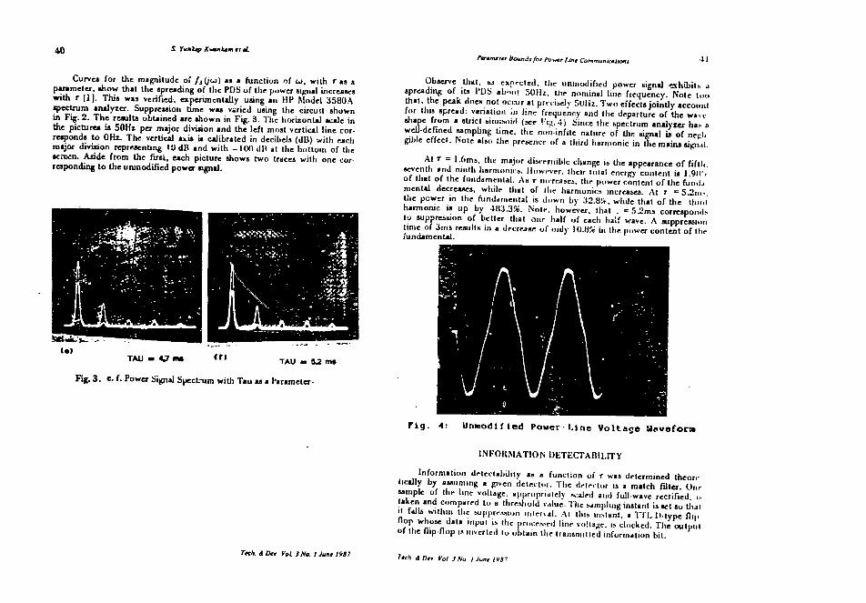

INTRODUCTION
The project document was signed on June 28 1985According to this document progress reports were to havebeen submitted within thirty days of the following dates December 31 le8s June 30 1986 and December 31 1586 This has not been done for the reasons given below
The PERT chart in the work plan indicates times withrespect to the date of availability of the neccessaryequipment The first batch of project equipment purchasedin the US in AugustSeptember 1969 was delivered onDecember 24 1985 There were also some delays in gettingthe space allocated to the project prepared for installation of the equipment The result of all this was that theexperimental aspects of the project did not begin untilFebruary 1986 The first
written in format by
March 1986 and represented report was results some
therof
efore written which
in were
already obtained but mostly anticipated
In the absence of any guidelines the report was a summary the Principal Investigator
(PI) The PI also indicated in his covering letter -thatshould the format be found inadequate he would redo thereport according to the guidelines provided Fred JBieganskis letter of February 12 1987 to the PI is the first official reaction to the report
PROGRESS MADE IN WORK PLAN
Before undertaking a hardware simulation of theproposed technology at nominal power line voltages and currents it was deemed necessary to carry out a lowvolatage simulation The advantage offered by a low-voltagesimulation was that the encoder and decoder systems could bemastered without delving into problems posed by operation atthe nominal values since these systems remain essentiallyunchaged even at high voltages and currents
A low-voltage simulation was realized and used to testthe physics of the scheme Details of the simulation appearin the paper entitled Low Uoltage Simulation of a NewDigital Power Line Communication Technololgy see Appendix 1
The next step was to implement the encoder and decoder systems using microprocessors as opposed to the discretelogic circuits of the low-voltage simulation These sstems are now implemeted using the Motorola MEK6802DS single-boardmicrocomputer This has enabled easy modification of systemparameters such as suppression time and the study of theireffect on detectability and spectral distortion The results
2
obtained for the low-voltage simulation which appear in the paper entitled Parameter Bounds for a New Power LineCommunication Technique Using Waveform Modification(Appendix 2) have also been obtained at the nominal line voltage of 220 volts
The lcw voitage simulation exploited the voltagesuppression scheme in the control mode ie loads werecontrolled remotely from a given point With themicroprocessor implementation a data transfer and aspectrum analysis mode have been added In addition aninterface for the MEK68O2DS has been ralized which permitsblocks of data to be transferred from a microcomputer withsecondary storage through the parallel printer port intothe MEK6BO2D5 for serialization and transmission A paperbased on the abstract shown in Appendix 3 is in preparation
The interface between the encoder and the power line isthe injection circuit This is what causes suppression ofthe line voltage for a Fixed time beginning with the zerocrossing when a binary 1 is transmitted Three types ofinjection circuits have been examined but only one indetail as indicated in the paper entitled Injection Methodsin a Digital Communication Scheme Using Power SignalWaveForm Modification see Appendix I We have fixed onparallel injection Two configurations are possibleparallel injection with a series pass element and parallelinjection with a shunt element Currently only the series pass element configuration has been implemented
In terms of the work plan these results represent theaccomplishment of only items 1 2 3 S and 6 of Phase 1 ofthe project However from what we now know they representbetter than one half of the effort and time required toaccomplish all the objectives of the project contrary towhat is indicated in the PERT chart Phase 2 workexample simply
for depends on the presence of a reflected waveand the detection of positive and negative peaks as opposed
to positive- and negative-going zero-crossings Theimplementation of the encoder and decoder using single-boardmicrocomputers should reduce Phase 3 work to primarily that of assembler language programming A revised schedule is shown below
EXPENDITURE
Out of a total budget of One hundred thirteen thousandFive hundred forty-four dollars ($113S54) a total of aboutFortg-two thousand seven hundred seventy-six dollars($42776) has been spent The expenditure breakdown is as follows
- Equipment - $31129
- Technician salaries - $ 3192
- Overhead - $ 2455
OCFA expenses have been converted to US dollars at 350 F$
OUTPUT SO FAR
The following qLint4fiable outputs have been obtained so Far From the project
3 papers presented at ANSTI-EE 86 International Electrical Engineering Conference Dar es SalaamTanzania Aug 18-20 1986 and one abstract(The paper on parameter bounds will also appear inUol 3 no 1 of the journal Technologa and Development)
- a low-voltage simulation oF the technology
- a 220-volt implementation of the technology for unidirectional communication from generator to load
UnquantiFiable outputs include a significant amount ofinstitution strengthening The facilities provided throughthe project are the main equipment support of the Automationand Control Laboratory (ACL) of the Ecole NationaleSuperieure Polytechnique (School of Engineering) of theUniversity of Yaounde The ACL currently numbers ten Fullshytime faculty members of the Electrical EngineeringDepartment and two associated researchers From outside thePolytechnique The ten faculty members represent two thirdsof the Electrical Engineering Faculty and one sixth of thetotal Polytechnique academic staff Most of the output ofthe ACL (see enclosed brochure) is directly or indirectlyrelated to the facilities provided through the projectThese outputs have in turn attracted other grants andactivities to the Laboratory
DIFFICULTIES ENCOUNTERED
We have encountered two types of difficulties onetechnical and the other logistic The technical difficulties have to do with tha supply of equipment and components
The unavailability of certain electronic components inCameroon has caused long delays in the project Inelectronics work one cannot determine in advance all the types of components that will be required on a project Thepossibility of easily picking up components as the needarises must therefore exist if the project is not to besubjected to severe delays This is not the case in Yaounde
4
Some components have had to be ordered from the US Andbecause the quantities are very small the orders are not ofcommercial interest to most suppliers Those isolatedsuppliers who are willing to handle such small orders are inno big hurry to Fill them either The project has thereforesuFferred severe delays par-ticularly as concerns therealizazicn of the injection ciucuits Technical details onthese difficulties are given in Appendix 5
The second type of difficulty encountered is logisticalsupport primarily transportation Lengthy arguments wereadvanced in October 138S as to why a transportationcomponent should be included in the supplemental budget (seaAppendix 6 For excerpt) This aspect of the request was notapproved Those items which have been purchased locally havetherefore necessitated the absence of some member of theresearch team every time a purchase is made And given theimpcssibility of calling in advance to determineavailability some outings have been tours of the city
In addition to this expenditure in time justifiableexpenses have been incurred which unfortunately cannot bedocumented in a manner acceptable For reimbursementCameroonian taxi drivers and bus drivers do not givereceipts And when the Pls personal vehicle is used thereis no way of documenting this other than by odometerreadings It is not clear if and how these readingstranslate into project dollars So claimsno have beenmade Finally receipts From purchase of gasoline areinappropriate since the vehicle is not used exclusively For project activities
MODIFIED WORK PLAN
The work plan is essenitially unchanged What haschanged is the schedule The modified schedule is as shown in the PERT chart attached
CONCLUSION
The scientifique basis for the proposed technology issound We therefore cnntinue to hold high hopes For thisproject despite the difficulties we have encountered Theseall stem from working with Fairly sophisticated devices in an environment which lacks the support system - in this caseprimary and secondary sources For components - on whichadvanced teci-nologically must rely
5
April 1967
0 Time in months
PHASE I
1
2
3
REVISED ACTIVITIES SCHEDULE
3 6 9 12 15
S
PHASE II
2
3
PHASE III
A MULTILEVEL MULTIPROCESSOR SYSTEM FOR AUTOMATIC DATA
LOGGING IN A NEW DIGITAL POWER LINE COMMUNICATION SCHEME
by
S Yunkap Kwankam N Ntomambang Ningo and F Nematchous Automation and Control Laboratory
Ecole Nationale Supgrieure Polytechnique University of Yaound6
SUMMARY
The robustness of a technique for transmitting digitalinformation on electric power lines using waveForm modification first suggested by Kwankam Ei] and implementedby Kwankam et al C23 is tested by measuring its immunity tovoltage amplitude variations frequency fluctuations andvoltage waveForm changes As -transmission rate is only 100bits per second (limited theby number of zero-crossings per second) a system For unattended transmission reception
errorand automatic logging becomes imperative if statistically significant amounts of data are to be logged
The system is a multilevel multiprocessor data loggerText resident in a File in a microcomputer C an ATampT PC6300) is down-loaded 8 K butes (characters) at a time to aMotorola EK68O20S single-board microcompuLer The 6802board then introduces parity and other bits appropriate tothe protocol used and transmits the characters out on a power line Transmission is bit-serial At receivingtheend a receiver-decoder implemented on another Motorola MEK680205 recovers the individual bits checks for anyerrors and assembles them into characters The assembledcharacters are then uploaded again 8 K bytes at a timm toanother ATampT PC 6300 microcomputer The microcomputer in turn saves the received text in another disk file
On downloading communication between the PC 6300 andthe 6802 is through the parallel printer port of the former and the peripheral interface adapter (PIA) of the latterThus a data transfer rate of 50000 bits per second (limitedby the 4-MHz clock of the 6802) is readilW acheived withoutadditional hardware This is significantlU higher thanhigher than the 9600 baud available through the use of theserial port and thus frees up the the PC 6300 to performmany other tasks in between servicing the 6802 on an interrupt basis
Uploading is done by means o an interface usingminimal hardware which occupies one of the slots on thesecond PC 6300 and the IN instruction in an assemblerlanguage code The control programs in both PC 6300s arewritten in BASIC Data transfer rate on uploading is about20000 bits per secono
The system is capable of logging date continouslUuntil the source disk is empty (and the destination disk isfull) For Floppy disk files this takes about 10 hrswhereas For Files on 10MB hard disk systems data transfer can go on for 275 hours non-stop Using this system therobustness of the communication technology has beenthoroughly tested with minimum human intervention Itsadaptation to other environments where unattended logging is unavoidable is straight-forward
data
2
APPENDIX 5
Parallel injection with a series pass element meansthat the load current Flows through the switching device inthis case a thuristor The thgristor is Fired at the zeroshycrossing to transmit a 0 or is Fired aFter a delaycorresponding to the suppression time to transmit a 1 Inthe latter case the voltage waveform is therefore suppressed as required by the theory However the currentFlowing through the line depends on the nature of the loadSpecifically when the load is resistive the thyristorcurrent goes to zero at the voltage zero Thus the voltagewaveform at any point downstream of the point oF injectionshows suppression beginning at the zero-crossing If thetotal load is not resistive there is a phase shift betweenvoltage and current The thyristor current does not go to zero at zero voltage but some time before or thereafteraccordingly as the load is capacitive or inductive In our case the load is inductive Uoltage suppression therefore starts some time after the zero-crossing the more inductive the load the later this occurs
Suppression can be returned to the zero-crossing byphase compensation A capacitive isload connected inparallel with the inductive load The capacitive load ischosen so that It resonates with the inductive load at the line frequency 50 Hz in this case The small inductancevalues oF the load when a transformer is used to tap of themodified signal for detection purposes require unmanageablecapacitance values ( around 1 F) To reduce this toobtainable values transFormer-coupled capacitancecompensation has been employed A second transformer hasbeen used whose net effect is to multiply the capacitance- as seen From the primary side (the line) - oF thecapacitor connected across its secondary This has worked quite well in terms oF reducing the displacement oF thesuppression from the zero-crossing However minor problemsstill exist beacuse the suppressed portion of the signal isnot Flat (zero) This simply translates to a more elaborate detection algorithm in the microprocessor-implemented decoder
All oF this could be avoided by using a shunt elementconfiguration in the parallel injection circuit This can bedone with either h gate turn-off (GTO) device or atransistor Use oF a thyristor would imply Forcedcommutation and therefore voltage suppression would not betotal We have not been able to Find either a GTO device or a high-volatage swithching transistor (which does not have aFree-wheeling collector-emitter diode) Welocally havetherefore had to order these And given the insignificanttotal dollar value oF tie purchase we have the delaysindicated above
INJECTION METHODS IN A D(TAL CO(M-IJNCATIGN SCHEME USiNG POWER
SIGNAL WAVEFOHM MODIFICATION
by
S Yunkap Kwankam JM Ngundam S Tchouate F Nematchoua E Ondoua and Awono Onana
Automation and Control Laboratory Ecole Nationale Supericure Polytechnique
University of Yaounde YAOUNDE Cameroon
This research has been carried out under a grant from the UnitedStates Agency for Internaational Development (USAID) under itsProgram for Science and Technology Cooperation (PSTC) AID project no 936-5542 proposal no 5204
Abstract
This paper presents the results of investigations into threemethods of achieving power line signal suppression in adialtal communication scheme
new which uses power signal waveform
modification The methods are (1) series injection throughmutual induction of a 180-degree phase-shifted version of themains (2) series injection by use of a third winding on a transshyformer as the control input and (3) parallel injection by use ofboth shunt and series pass semiconductor switching elements Ineach case the efficiency of the method is measured as the amount of suppression for a given modulating signal of known power
Parallel injection using either thyristors or transistors isshown to be far more efficient than the series injection methods
3
INTRODUCTION
In a new digital communication scheme advanced by Kwankamand others (1-3] the poer signal waveform is modified to encode 7 n o ss n s s -s rr re i- -a
reports on the experimental investigations of three methods ofachieving signal suppression In each case the efficiency of themethod is measured as the amount of control signal power requiredto suppress a given power line signal for a fixed duration
SERIES INJECTION
Consider two electromaanetically coupled circuits as shownin fig 1 [4] We are interested in the conditions under whichthere is a net transfer of energy from one circuit to another It can be shown that for currents i and iwith a variable phaseanale difference one circuit will provf-e more energy to theother than it receives from it for some value of the phase angledifference The currents are
1i = 11 eJ(wt + 91) (1)
T2 = 12 ei(wt + e2) (2)
The complex powec due to the coupling is 9Irl= = 12 eJ ( 2 - (3)i )wM I2 81)
= = 2 jWMIlI 2eJ - )2) (4)
where
means complex con)ugate
(3) and (4) may be written as
31 = wM 2 11 sin(0 2-81) + jwMI 2I 1 cos(e 2-e9) (5) =S2 wM211 sin(8 2-el) + jwMI 211 CoS(E 2-91 ) (6)
learly 31 = -S2
Active and reactive power are given by
P = -P2 = WM211 sn(82-eI )
for active power and
81 = 02 = wMI2 11 cos(9 2 -31 )
for reactive power
Fig I Two electromagnetically coupled cLrcuts
C
Fig 3 Phase shift regulation circuit
~ UA I
r II6
u
Time
t
(a)
iI 1 A -
E
(b)
Fig 2 Instantaneous circuit variables for
(a) power line (b) injecting circuit
4
Depending on the time interval considered energy transfer
could be positive or negative Positive power transfer means that
there is a net transfer of energy from the source considered
h e ne7 r- erns 3 net t ansfer of enerqy to the source
If 91- ( lt 0 then P1 gtO and P2 lt0 Therefore the first
circuit is tranfering power to the second circuit On the other
hand if n_ 10 then P20O and P (0 The roles of the circuits are then regersed Now suppose that the firsit circuit is a power
line and the second is a circuit injecting energy into the power
line Then we have
= 71 sin wtV0
72 = -V1 sinwt = - V1 sin(wt + ()
i2 - I2 eJ(wt + i + 02)
For the injection circuit to transfer power to the line we must
have
gt 8 2 + 81 gt 0
Maximum power transfer therefore occurs when 82 = Tr2 - 81 Generally in a well regulated system the power factor is of the
order of 08 with a value of -n6 for 81
Figure 2 shows the instantaneous power P1 of the power line and the power P2 of the injecting circuit Notice that P1 is negshyative and is positive at the moment of signal suppressionP2
A circuit which may be used to provide phase shift regulation is shown in Fig 3
The coupling betueen the circuits of Fig 1 is limited by the fact of the flux linking them having to pass through air a
low pemeability medium In a bid to decrease the losses in the
flux linkage between the circuits we conceived a three-winding transformer showm in Fig 4
THREE WINOING TRANSFORMER
We have a magnetic circuit on which there are three separate winshydings
a primary winding with n turns
a secondary winding with turns andn2
a tertiary winding with nc turns
SC
v()Wn VC o- -- -- 4
_
4-
Fg 4 Three-winding transformer for n)ection control
5
The primary and tertiary windings are wound in oppositedirections with = nl When Snc is open the system operates as an ordinary two winding-transformer Let us examine this case in more det i
V1 (t) =Vim cos wt (9)
In the magnetic circuit we have
V1 = -el = n-dG (10)
dt
where
60 is the open circuit value of the flux and is given by
Vlm = - cos(wt-ff2)6 O (11)
n1w
We notice therefore that at constant frequency the flux dependsonly on the voltage
At the terminal of the secondary winding we have
d6o V2 = 12 = -n shy (12)
dt
When the switch S is closed we have
V1 = jLiwIl + jMw1 2 (13)
V 2 = -jL2 wI2 - jMeI1 (14)
n1ll + n2 12 = nII1 0 (15)
At open circuit (i =0) with switch S closed a fluxsecond opposite to the firs is produced as a result of current flow in the tertiary winding Thus
Vim Vim 1 - 1= - cos(wt-r2) = - cos(wt-ff2+ff)niw u
Vim -i cos(wt+ff2) (16)nim
The resultant flux in the magnetic circuit is theoretically zero
V
D
D 7406
RL = 2 7-a 5 W
D = IN5341B
R8 = 12 -a
Rc = 330JI
R = 10O-Q T = (Schc ffner) IT 313
Fig 5 Control circuit for parallel injection
7
RESULTS AND CONCLUSIONS
We m~y define the inefficiency n of a particular in)ectionmethod as the amount of injected power required to suppress agiven amount of line power as a percentage of the latter The results obtained show that the parallel injection methods are theleast inefficient while the series methods are the most wastefulThe computations show that the series injection method requiresat least as much power to be injected as that which is to besuppressed not counting losses In the three winding transshyformer these losses are such that when the inputs to the twoprimaries exceed 120V it requires an additional lOZ of the powersignal to obtain total suppression On the contrary the injected power in the case of the parallel methods may be considered asthe total dc power dissipated by the circuits driving the gatein the case of an SCR or base in the case of a transistor This was measured to be around 18W The line voltage suppressed was 220V rms Assuming a minimum load current of 1OA and thatsuppression time is a line2 msec on 50Hz we find that the inshyefficiency is a scant 8
REFERENCES
1 Kwankam S Yunkap Principles of a Digital Communication Scheme Using Power Signal Waveform Modification Technologyand Development Vol 1 no 1 Dec 1985 pp 23-40
2 Kwankam S Yunkap Ngundam JM Ningo NN and NgamyDT Low Voltage Simulation of a New Digital Power Line Communication Technology ANSTI-EE 86 Electrical EngineeringConference University of Dar es Salaam Dar es Salaam Tanzania August 18-20 1986
3 Kwankam S Yunkap Ningo NM Bilikha JB and NgamyDT Parameter Bounds for a New Digital Power Line Communishycation Technique Using Waveform Modification ANSTI-EE 86Electrical Engineering Conference University of Dar es Salaam Dar es Salaam Tanzania Aug 18-20 1986
4 Etoung LH and Nyemaeck N Realisation dun Simulateur pourTransmission dInformations Numeriques sur Lignes Elecshytriques final-year project report ENSP University ofYaounde June 1985
5 Mak ST and Moore TG Jr TWACS a New Viable Two-WayAutomatic Communication System for Distribution NetworksI Inbound CommunicatLon paper 84 WM 182-2
Part IEEE Power
Engineering Society Winter Meeting Dallas TX Jan 29 -Feb 3 1984
6 Mak ST A new Method of Generating TWACS Type OutboundSignals for Communication on Power Distribution Networks paper 84 WM 181-4 IEEE Power Engineering Society Winter Meeting Dallas TX Jan 29 - Feb 3 1984
PROJECT N 520 DIGITAL INFORMATION TRANSMISSION ON
-E CTRICAL POWER LINES
PROGRESS REPORT March 4 1986
This report covers progress made on the project since the grant documant was signed on June 28th 1985
Purchase of equipment
The prinpipal investigator took advantage of his visit to the US as a ibright Visiting Scholar during the summer of 19SB to purchase most of the basic equipmentneeded by the project These included the computer systemsthe spectrum analyzer and sufficient components to completethe low voltage simulation of phase 1 of the proposal
Experimental Work
A hardware implementation of the technology on a low voltage (30-volt) line has been completed Two lampsconnected to the same 30-volt source are independently controlled by two switches using the technique
Work continues on various injection methods where parallel injection using a pass thyristor seems to be the most promising
Publications
One paper (see appendix 1) has been published on the principles of the technology Four other manuscripts are in preparation for the ANSTI EE 86 Electrical Engineering-conference scheduled for August 1986 in Dau es Salaam (see appendix 2)
Supplemental Budget
A supplemental budget of Sq6350 was requested in October 19BS Of this amount S2SOO was recommended For approval Further purchase of equipment awaits final approval of this budget supplement
Recd in SC NOV 4 1988
0
~1II
UU
rUL
LW
4
c
-
~~t
~aoJ
a ~
~ u
tAshy
44C
4
U
2
0
N8 CL-
CF
i4
1-~ 0
-
--
I --
0 C
-)
LQ
~
24
25
S Y Kwani2n Nou~s aLons decrit en ddtail une methode on IVioninnattt htnare est ode ar lag
presence ou lab sence du signal de puissance r la gne pendant un tntr alle hie nd e i nt cvonmrneItanr iI chaque crosement a ziro Un code I en supprtmant lesignal et ) en tie lemodifiant pas
Les pnincipes de Vencodeur que nous arons ddcrtts unt lutlitIrate di usignal de puissance modifie dune aiiallsecodee ont ite egalement decritesen deads Les cnteres er les De uxnetjades de 3pec-Jde -tc) ie a eqiie ne binaire
che rtdes pamm etres de do n nes La different t relationrqut dteterfntnett Ict t ontn eleure tethodiepermettant
int de rn inniserla distortion ispectrale
a natdi et titla tnestgn ial uise sance
INTRODUCTION
The need for transmitting information on electrical power lineshas existed eversince the advent of electrical power distribution networks SlIIe control functions needto be exerctsed at various points in the network for load management fault Isolation andother purposes it is economically advantageous to use the wiles themsehesmunication link This idea was advanced as early as as the comshy
1898 by Routin and Brown I I
There are currently two basic approaches to exploiti g this idea T hietraditionalapproach in operation since the latecommunication systems f21 19 20s has been through the use of ripple controIn these systems narrow-batwfrequencies between ( 1-20 Hz) pulses with carrier100-1000 Hz arestations Tie
injected into the power lines at distribution subshysame principle of carrier-bome signal injection s used for voice commushynication between stations-on power networks [3]
More recently attempts have been made to develop communication technologiesDased on the use of the 50-or 60-Hz power signal as the earner Direct-aton schemes for digta communication include flattening of the waveformwaveform modii-Ftops 14rodmodulation of the location of the zero crossing [5] The latter scheme wasdeveloped)yArthur D Little Inc ofCambridge Massachusetts
THE YAOUNDE SCHEME
The scheme described in this paper is currently under investigationrationale Supirieure Polytechnique of the at the EcoleUniversity of Yaounde Here binary infor-iauon is encoded as the presence or absence of the power signal oathe line during a
Tch J Dev Vol 1NoI lec IY8J
I l ieI
wejl-hciiel itiicviilegonig tlih eChCI Lzeti tus~itg (ihl~ded by suppie siing ilhes g al an d t) y lc auig th e s glJau n moi d as show [g I
ca r e BIT
0
A 0at
d car ie
Fig 1Typical Wavefoms -the Ya centur IeSheme
Aside from thecoming of the ADL schemeneed for originality this researchModulation of the intivated hy a major shortshypredicated on the assumption zero sviesof thethat the line frequency is power signal istv ightly contrulled Ilhisishave shownnot tile casethat iine frequency varies between 48 and 52 Ii It)] in the local electrical environment in Caiclti Informal measurementsworkable The Yaounde scheme is
no matter what the line frequency variations acedent on the foi n Ili addition it is not depenshyof tie power signal as long as this stgia is strictly monotone aroundthe zero crossings
Tedh 1 Des Vool I ec1985
26 27
S Y Kwankam I) tug-jIPower Line (mnJ4
switch ht all lllvcrllli amplifier Fie zero crossing ainti p I A --ileand using
co m pai l r a re sei o ilia t th e a n a og switc h is Iu iO i- n s11holy t le and t u-ehr ne d oit slofrltv itter each zero crossing seeLOAD I of that of I Fig 5 The gaint lihe niplifit is the ieciprocalthe attentatOr lhus the signal at the output 1 he sinpidies when the switch
CONTROL FACILITY
LOAD N
RCS =Remote Control Switch Fig2 Model of system for the Yaounde Scheme
The scheme is designed for use in any electrical environment which can be modelledas shown in Fig 2 Examples include a low tension network served by a single substationa set of substations served by a single medium tension tr3nsmision line and the entirenetwork uf a micro- or mut-hydro facility Remote control switches (RCSs) I throughN are turned on and off to supply or cut-off power to various loads In the system current-ly under investigation each RCS is given an eight-bit identification code and each transshynsion conssts of 15 bits For a 50-1z line a single controller can thus access all 256RCSs in the system in 384 seconds
ICA
AA
ENCODING PRINCIPLE
To encode the binary intormation the zero crossings of the power signal are de-tected and the signal i left unaffected for a 0 or surpressed during r seconds for a ISignal suppression is hieved by adding to the signal a 180-degrec phase-shifted versionof itself A tinctionia block diagram for the encoder is shown in Fig 3 and furtherelaborated in Fig 4 The power signal is attenuated and then fed through an analog 14 l-shy
0O
I
Tech d De Vot 1No1 Dec 1985 Tech d Dev ampVJ 1NoI Dec 1985
28
19
S YKwankam
is oi is equal in magnitude but opposite in polarity to that at the input ) [lile attenuatorZero crossing detectors (ZCDs) are used to trigger monostable multivibrators such thatthe pulses at the output of gate OR I occtr within the onshown in Fig 5 le tine of the analog switch asamplifier output has-thereture stabilized before any signal injectionoccurs The pulses at OR I are ANDed with the bit to be transmitted D LJT to providethe control signal to the injection circuit Typical injection ircuits beng investigated appear in [2 7]
I
II
- Z If
D -1
J CL4DcK
I
ORt ljjJ 1i
Fig 5 Triming diagram for the encoder
It is assumed that the control program for the scheme is storedmemory for examole The - in computer15 bits which constitute each block of information are trans-ferred from storage into a buffer In the current simulation the buffer is accessed every150 milliseconds and theclock for this circuit istakenlaaa serialized by the circuit showii functionally in Fig 6 Thethe output of gate Al1of Fig 4
The encoder circuits have becn definedwith only minimal consideration for reducingthe hardware cost The emphasis has been on accurately encoding the binary input se-quence using the waveform modification scheme described By contrast cost reductionplays an important part in the design of the decoder This is justified by the considerationthat there can be as many as 256 decoders for each-encoder in the system
FREQUENCY SPECTRUM We now consider the frequency spectrum of the modified signal Let FO(s) and F (s)be the single-sided Laplace transforms of the waveforms associated with the transmission
Tech amp Dev Vol 1 No1 Dec 185
Ditil oer ne (ommun
of a single 0 hit and a single I bit respectively ie Fo(si i ifte transfujit of the positivehalf of a pure sine wave Then ie waveform associate itihthe transmission of the binary sequence 1 b transforms by the time delay iipelty toF(aj = plusmn [(b ( Om)lt s + (b (D I)Fo(s1 o
-b reg O)Fds exp( -rw 0o -(b C) )F(l ekxpt-rwo
0
+(b Q t)DFt() (p( -21lrw)
+(b (D I)Fo(s) expf -2asrw) + I 1where wQ is the frequency of the unmodified sinusoid and Q represents the logicalExclusive-OR operation The plus sign is selected if bo is iansnitted at a zero crossingof positive slope Othenvise the minus sign is chosen
It can be easily shown that for the carrier of(]) at1 at uming an amplitude of Ivolt and transmission at a zero crossing of positive slope
F5(s s2 + exp-xirWoJo (2J0
Tech ampDer Vol 1 No Dec 1985
+ 7
-~
~- ~
77
70
I L
7
a FT
RN
4
~~ 1 R
Vy 1F7
-44~
p-1
~154
~~IT
~_41
-+
~---2
~
h+ ~c
-le +
-+
LL
~ +
~ al
~pW
~~p
~
~ +
V
ttc
EO
0
P jN
~1-
C
a
-I LFi-
-1
~ 4
~
34 S Y Kwankam
a detector which does not operate on the demodulation principle
Two different methods of one-step detection of the binary sequence are currentlyunder investigation In the first method the modified sinusoid - or some fraction thereof - is rectified and sampled at somewhat follows time instant to during the suppression time (Intime is measured from the nearest zero crossing of the correspondingmodified sinusoid) This sample un-is then digitized by latching it into a flip-flop as either
a0 or a 1see Fig 9
0alt)DT DATA
LTCH
CK OUTPUT
COMPARATOR ONE WITH SO
IHYEIS SHOT
Fig 9 Scheme for one step detection of encoded bits
The corparator-with-hysteresis server as a detector (In actual operation an antici-pator) of the zero crossings The monostable multivibrator provides apling occurs delay so that samshypreci-ily at to The multiplier a as shown below is a nonlinear function ofvin This is because dtrinampsuppreaion time the sampled voltage for a transmitted 0 mustsansfy the input threshol conditions for the type of logic technology employed whilethe same signal must not exceed the maximum allowable input voltage at any time Thehardware is chosen such that a is a constant during suppression timeSuppose the flip-flop has the following characteristics and vv0 are the maximuminput voltage corresponding to a logic 0 and the minimum input voltage corresponding toa logic 1 rea ctively ts is the set-up time for data input and th is the hold time for datainput (after T clock transition) Then correct detection of the encoded bit requires that
(wint)gt Y1 fo-ts lt I lt to + th t7)
to is reated to r by the inequality
to + th lt r (8) If the corparator-withhyteresia Is simply a Schmitt trigger buffer of the same logic family w e-asohave
Z-champDe Vol 1NoI Dec 1985
bull
tl Poier line Common 35 15Vtnt) ro 0o lt I t
(9) where t s te time delav between the 1-to-0 t in of the output ot the bufferand tilenext zero crossing-
In(9)we have ued the symnetrN of the ectified sjjiout tie zero crossng when nh e e ed t s f t
Criteria for chosing C 7 toand t1
two importint criteriaIn ( 7) and lr the only parameters leftinvolved to our ctwicein tile choice otT We kho re a r t( and ti There are
(i) tinimnte pectral distoltion ard (ti) maximize the distinguishability of the signai responding to encoded 1ancorrespondig to an encoded 0
The choicechoice ishowever jgreatly ofinfluencedparamountby a Given awe of - thus importance to ire success ot the scheme Thisrmusthuose r such that
rint)I t =nf2w o (10
where vm is the maximum aiiowable input voltage for thLilc technology used
Taking the equality in (8) and substituting for to + th I asJ well as fbr vin in (7) and(10) we obtain
Q I i
Taking v = 25 volts vm 50 volts typical values for Il1 ntes and A= 220 volts the bounds in (lI deiiie an interval
choice l1T only if rgtrt6wo Th early violaies criterion (i)above for tile
This predicament is avoided by making ota nonlinrc minrction of v In paiticuIr (vin) as shown in Fig 10 where inmits the choice the nonlinear regio u ries inverSely with vii perof mrch smaller values fordistortion a functtotns of this type and thcreie 1re lfTrimiathon of spectr-lcan be readily realizcu ncrig commonly used circtitelements ithe present investigation ko 1
With (10) satsritpd and a I during suppression ti -mtntlie smallest allow able value
Tech amp Dei iol INo Dec IY85
C
36
37
S YKwonkam Digital Power line Communiati
a
0(
0
Vo SFig1i Juaa function
l1enak ltlt1
In e curve for fuuther miinizatln o spectral diutortion - ktgt
Fig 10 Phl u1Ivplpi a curve wilichmImozessp rili$1ukllolinearregiona varies iversely withVin)
4 d in non
for r is found by taking the equality in both (7)ant (8) This gives
Tmin = (lwe) sid (iVlA) + ts+ th (12) Choosing the equal sign in (8) clearly fixes the value of to And since a is now determinedti isread ound from (9) to be (1w 0 ) s nf (vdA)
It should be noted that the criteria indicated above do not invariably lead to theexpreWsions obtained for the various karameters rfor example can be greatly reducedby making tie parameterc ajump functon Of in
-As in Fig 11 a could be very large during sunpression time and very small or evenzero at other tunes Similarly the comparatoi-ith hysteresis could be made to approxishymate a zero crossing detector quite accurately by using the circuit shown schematicallyin Fig 12 in which t can be mad~e arbitrarily close to zero Thes refinement howeveronly add to the complexity of the detector Sini- every branch transmission line aadultimately very subscriber implies one such detector it is of great economic imnortanceto keep the aetec3r as simple as possible Reliability considerations also dictate that thedetection process oc uncomplicated
VR2
Vin
VRI
+ X0 Cc
MUX Y
+
Yiamp U Schrmc of cornoarstor with hyuieruis usedfor Zero The i-I transitionO Bc ico n t o cur ritrsi
-ng
KlL
i ilteinstion Mteo thsetrocros
Q
Tech amp Dev Vol NoI Dea 1985 Teds D Dev Vol lVo1Dec 1985
39
38M S Y Kwankam
DtgraPower Ui e Communication
AN ALTERNATE APPROACH Clearly a I can be detected without examining the output of the zero crossing detector A second method of T ieepdetection which is aiso under ivesigatun is a diffe-Aeciond methed However givenrentiation scheme- The mf--tedetstignlwich the Inherent tendency of differenttatorsied signal is attenuaed andr to emphasize the noise inand ivesttiatdns amilu is attlnuao differenttiated andheand the en- signal Inclusionadded of the outout of themeasure of noise immunity zero crossing detector In detecting a 1 providescoded hits detected as show n shematicallv in Fig 13 The waveforms inthis method are
an as shown in Fig 14 Each pair -f adiscent jumps in the differentiated signal indicates the transmission of a 1 The eznoed bits are then detected according to the conditions inTable 2
-t 0 s
Ithto
FIg 14 Modulated signal for the sequence 01 10-V(t) and its derivative V(t)
CONCLUSION
The Yaounde scheme offers the promise of an altemative method of digital inforshymation transmission on electrical power lines by waveform modification of the powersignal The advantages and disadvantages of the schenz- compared tu other techniques ingeneral and the ADL scheme in particular will be more clearly known after eper mentalC(dition Bit detected data have been collected Examination of the principles shows that the Yaouhde schemeZero crosstng detector trigered and no edge in v(t) 0 overcomes the need for tight control of the line frequencyThe two detection methods analyzed both
tas seemZero crossing detector tri~gered and edge in v(t)
adequate for recovering the transshymitred binary sequence However noise Immunity considerations apart the differentiashytion methou has the advantage that the effect of r on the detectability of the encodedToble 2 Detectiona cnditions for differentiator-based detector for even extremely small values of tbits Is greatly minimized - the edges in the differentiated signal will occur in principleIn theory then spectral distortion can be minimized
Trch amp Der INa1 Dec 1985 Techa Dev Vol 1 No1 Dec 1985

4
Depending on the time interval considered energy transfer
could be positive or negative Positive power transfer means that
there is a net transfer of energy from the source considered
h e ne7 r- erns 3 net t ansfer of enerqy to the source
If 91- ( lt 0 then P1 gtO and P2 lt0 Therefore the first
circuit is tranfering power to the second circuit On the other
hand if n_ 10 then P20O and P (0 The roles of the circuits are then regersed Now suppose that the firsit circuit is a power
line and the second is a circuit injecting energy into the power
line Then we have
= 71 sin wtV0
72 = -V1 sinwt = - V1 sin(wt + ()
i2 - I2 eJ(wt + i + 02)
For the injection circuit to transfer power to the line we must
have
gt 8 2 + 81 gt 0
Maximum power transfer therefore occurs when 82 = Tr2 - 81 Generally in a well regulated system the power factor is of the
order of 08 with a value of -n6 for 81
Figure 2 shows the instantaneous power P1 of the power line and the power P2 of the injecting circuit Notice that P1 is negshyative and is positive at the moment of signal suppressionP2
A circuit which may be used to provide phase shift regulation is shown in Fig 3
The coupling betueen the circuits of Fig 1 is limited by the fact of the flux linking them having to pass through air a
low pemeability medium In a bid to decrease the losses in the
flux linkage between the circuits we conceived a three-winding transformer showm in Fig 4
THREE WINOING TRANSFORMER
We have a magnetic circuit on which there are three separate winshydings
a primary winding with n turns
a secondary winding with turns andn2
a tertiary winding with nc turns
SC
v()Wn VC o- -- -- 4
_
4-
Fg 4 Three-winding transformer for n)ection control
5
The primary and tertiary windings are wound in oppositedirections with = nl When Snc is open the system operates as an ordinary two winding-transformer Let us examine this case in more det i
V1 (t) =Vim cos wt (9)
In the magnetic circuit we have
V1 = -el = n-dG (10)
dt
where
60 is the open circuit value of the flux and is given by
Vlm = - cos(wt-ff2)6 O (11)
n1w
We notice therefore that at constant frequency the flux dependsonly on the voltage
At the terminal of the secondary winding we have
d6o V2 = 12 = -n shy (12)
dt
When the switch S is closed we have
V1 = jLiwIl + jMw1 2 (13)
V 2 = -jL2 wI2 - jMeI1 (14)
n1ll + n2 12 = nII1 0 (15)
At open circuit (i =0) with switch S closed a fluxsecond opposite to the firs is produced as a result of current flow in the tertiary winding Thus
Vim Vim 1 - 1= - cos(wt-r2) = - cos(wt-ff2+ff)niw u
Vim -i cos(wt+ff2) (16)nim
The resultant flux in the magnetic circuit is theoretically zero
V
D
D 7406
RL = 2 7-a 5 W
D = IN5341B
R8 = 12 -a
Rc = 330JI
R = 10O-Q T = (Schc ffner) IT 313
Fig 5 Control circuit for parallel injection
7
RESULTS AND CONCLUSIONS
We m~y define the inefficiency n of a particular in)ectionmethod as the amount of injected power required to suppress agiven amount of line power as a percentage of the latter The results obtained show that the parallel injection methods are theleast inefficient while the series methods are the most wastefulThe computations show that the series injection method requiresat least as much power to be injected as that which is to besuppressed not counting losses In the three winding transshyformer these losses are such that when the inputs to the twoprimaries exceed 120V it requires an additional lOZ of the powersignal to obtain total suppression On the contrary the injected power in the case of the parallel methods may be considered asthe total dc power dissipated by the circuits driving the gatein the case of an SCR or base in the case of a transistor This was measured to be around 18W The line voltage suppressed was 220V rms Assuming a minimum load current of 1OA and thatsuppression time is a line2 msec on 50Hz we find that the inshyefficiency is a scant 8
REFERENCES
1 Kwankam S Yunkap Principles of a Digital Communication Scheme Using Power Signal Waveform Modification Technologyand Development Vol 1 no 1 Dec 1985 pp 23-40
2 Kwankam S Yunkap Ngundam JM Ningo NN and NgamyDT Low Voltage Simulation of a New Digital Power Line Communication Technology ANSTI-EE 86 Electrical EngineeringConference University of Dar es Salaam Dar es Salaam Tanzania August 18-20 1986
3 Kwankam S Yunkap Ningo NM Bilikha JB and NgamyDT Parameter Bounds for a New Digital Power Line Communishycation Technique Using Waveform Modification ANSTI-EE 86Electrical Engineering Conference University of Dar es Salaam Dar es Salaam Tanzania Aug 18-20 1986
4 Etoung LH and Nyemaeck N Realisation dun Simulateur pourTransmission dInformations Numeriques sur Lignes Elecshytriques final-year project report ENSP University ofYaounde June 1985
5 Mak ST and Moore TG Jr TWACS a New Viable Two-WayAutomatic Communication System for Distribution NetworksI Inbound CommunicatLon paper 84 WM 182-2
Part IEEE Power
Engineering Society Winter Meeting Dallas TX Jan 29 -Feb 3 1984
6 Mak ST A new Method of Generating TWACS Type OutboundSignals for Communication on Power Distribution Networks paper 84 WM 181-4 IEEE Power Engineering Society Winter Meeting Dallas TX Jan 29 - Feb 3 1984
PROJECT N 520 DIGITAL INFORMATION TRANSMISSION ON
-E CTRICAL POWER LINES
PROGRESS REPORT March 4 1986
This report covers progress made on the project since the grant documant was signed on June 28th 1985
Purchase of equipment
The prinpipal investigator took advantage of his visit to the US as a ibright Visiting Scholar during the summer of 19SB to purchase most of the basic equipmentneeded by the project These included the computer systemsthe spectrum analyzer and sufficient components to completethe low voltage simulation of phase 1 of the proposal
Experimental Work
A hardware implementation of the technology on a low voltage (30-volt) line has been completed Two lampsconnected to the same 30-volt source are independently controlled by two switches using the technique
Work continues on various injection methods where parallel injection using a pass thyristor seems to be the most promising
Publications
One paper (see appendix 1) has been published on the principles of the technology Four other manuscripts are in preparation for the ANSTI EE 86 Electrical Engineering-conference scheduled for August 1986 in Dau es Salaam (see appendix 2)
Supplemental Budget
A supplemental budget of Sq6350 was requested in October 19BS Of this amount S2SOO was recommended For approval Further purchase of equipment awaits final approval of this budget supplement
Recd in SC NOV 4 1988
0
~1II
UU
rUL
LW
4
c
-
~~t
~aoJ
a ~
~ u
tAshy
44C
4
U
2
0
N8 CL-
CF
i4
1-~ 0
-
--
I --
0 C
-)
LQ
~
24
25
S Y Kwani2n Nou~s aLons decrit en ddtail une methode on IVioninnattt htnare est ode ar lag
presence ou lab sence du signal de puissance r la gne pendant un tntr alle hie nd e i nt cvonmrneItanr iI chaque crosement a ziro Un code I en supprtmant lesignal et ) en tie lemodifiant pas
Les pnincipes de Vencodeur que nous arons ddcrtts unt lutlitIrate di usignal de puissance modifie dune aiiallsecodee ont ite egalement decritesen deads Les cnteres er les De uxnetjades de 3pec-Jde -tc) ie a eqiie ne binaire
che rtdes pamm etres de do n nes La different t relationrqut dteterfntnett Ict t ontn eleure tethodiepermettant
int de rn inniserla distortion ispectrale
a natdi et titla tnestgn ial uise sance
INTRODUCTION
The need for transmitting information on electrical power lineshas existed eversince the advent of electrical power distribution networks SlIIe control functions needto be exerctsed at various points in the network for load management fault Isolation andother purposes it is economically advantageous to use the wiles themsehesmunication link This idea was advanced as early as as the comshy
1898 by Routin and Brown I I
There are currently two basic approaches to exploiti g this idea T hietraditionalapproach in operation since the latecommunication systems f21 19 20s has been through the use of ripple controIn these systems narrow-batwfrequencies between ( 1-20 Hz) pulses with carrier100-1000 Hz arestations Tie
injected into the power lines at distribution subshysame principle of carrier-bome signal injection s used for voice commushynication between stations-on power networks [3]
More recently attempts have been made to develop communication technologiesDased on the use of the 50-or 60-Hz power signal as the earner Direct-aton schemes for digta communication include flattening of the waveformwaveform modii-Ftops 14rodmodulation of the location of the zero crossing [5] The latter scheme wasdeveloped)yArthur D Little Inc ofCambridge Massachusetts
THE YAOUNDE SCHEME
The scheme described in this paper is currently under investigationrationale Supirieure Polytechnique of the at the EcoleUniversity of Yaounde Here binary infor-iauon is encoded as the presence or absence of the power signal oathe line during a
Tch J Dev Vol 1NoI lec IY8J
I l ieI
wejl-hciiel itiicviilegonig tlih eChCI Lzeti tus~itg (ihl~ded by suppie siing ilhes g al an d t) y lc auig th e s glJau n moi d as show [g I
ca r e BIT
0
A 0at
d car ie
Fig 1Typical Wavefoms -the Ya centur IeSheme
Aside from thecoming of the ADL schemeneed for originality this researchModulation of the intivated hy a major shortshypredicated on the assumption zero sviesof thethat the line frequency is power signal istv ightly contrulled Ilhisishave shownnot tile casethat iine frequency varies between 48 and 52 Ii It)] in the local electrical environment in Caiclti Informal measurementsworkable The Yaounde scheme is
no matter what the line frequency variations acedent on the foi n Ili addition it is not depenshyof tie power signal as long as this stgia is strictly monotone aroundthe zero crossings
Tedh 1 Des Vool I ec1985
26 27
S Y Kwankam I) tug-jIPower Line (mnJ4
switch ht all lllvcrllli amplifier Fie zero crossing ainti p I A --ileand using
co m pai l r a re sei o ilia t th e a n a og switc h is Iu iO i- n s11holy t le and t u-ehr ne d oit slofrltv itter each zero crossing seeLOAD I of that of I Fig 5 The gaint lihe niplifit is the ieciprocalthe attentatOr lhus the signal at the output 1 he sinpidies when the switch
CONTROL FACILITY
LOAD N
RCS =Remote Control Switch Fig2 Model of system for the Yaounde Scheme
The scheme is designed for use in any electrical environment which can be modelledas shown in Fig 2 Examples include a low tension network served by a single substationa set of substations served by a single medium tension tr3nsmision line and the entirenetwork uf a micro- or mut-hydro facility Remote control switches (RCSs) I throughN are turned on and off to supply or cut-off power to various loads In the system current-ly under investigation each RCS is given an eight-bit identification code and each transshynsion conssts of 15 bits For a 50-1z line a single controller can thus access all 256RCSs in the system in 384 seconds
ICA
AA
ENCODING PRINCIPLE
To encode the binary intormation the zero crossings of the power signal are de-tected and the signal i left unaffected for a 0 or surpressed during r seconds for a ISignal suppression is hieved by adding to the signal a 180-degrec phase-shifted versionof itself A tinctionia block diagram for the encoder is shown in Fig 3 and furtherelaborated in Fig 4 The power signal is attenuated and then fed through an analog 14 l-shy
0O
I
Tech d De Vot 1No1 Dec 1985 Tech d Dev ampVJ 1NoI Dec 1985
28
19
S YKwankam
is oi is equal in magnitude but opposite in polarity to that at the input ) [lile attenuatorZero crossing detectors (ZCDs) are used to trigger monostable multivibrators such thatthe pulses at the output of gate OR I occtr within the onshown in Fig 5 le tine of the analog switch asamplifier output has-thereture stabilized before any signal injectionoccurs The pulses at OR I are ANDed with the bit to be transmitted D LJT to providethe control signal to the injection circuit Typical injection ircuits beng investigated appear in [2 7]
I
II
- Z If
D -1
J CL4DcK
I
ORt ljjJ 1i
Fig 5 Triming diagram for the encoder
It is assumed that the control program for the scheme is storedmemory for examole The - in computer15 bits which constitute each block of information are trans-ferred from storage into a buffer In the current simulation the buffer is accessed every150 milliseconds and theclock for this circuit istakenlaaa serialized by the circuit showii functionally in Fig 6 Thethe output of gate Al1of Fig 4
The encoder circuits have becn definedwith only minimal consideration for reducingthe hardware cost The emphasis has been on accurately encoding the binary input se-quence using the waveform modification scheme described By contrast cost reductionplays an important part in the design of the decoder This is justified by the considerationthat there can be as many as 256 decoders for each-encoder in the system
FREQUENCY SPECTRUM We now consider the frequency spectrum of the modified signal Let FO(s) and F (s)be the single-sided Laplace transforms of the waveforms associated with the transmission
Tech amp Dev Vol 1 No1 Dec 185
Ditil oer ne (ommun
of a single 0 hit and a single I bit respectively ie Fo(si i ifte transfujit of the positivehalf of a pure sine wave Then ie waveform associate itihthe transmission of the binary sequence 1 b transforms by the time delay iipelty toF(aj = plusmn [(b ( Om)lt s + (b (D I)Fo(s1 o
-b reg O)Fds exp( -rw 0o -(b C) )F(l ekxpt-rwo
0
+(b Q t)DFt() (p( -21lrw)
+(b (D I)Fo(s) expf -2asrw) + I 1where wQ is the frequency of the unmodified sinusoid and Q represents the logicalExclusive-OR operation The plus sign is selected if bo is iansnitted at a zero crossingof positive slope Othenvise the minus sign is chosen
It can be easily shown that for the carrier of(]) at1 at uming an amplitude of Ivolt and transmission at a zero crossing of positive slope
F5(s s2 + exp-xirWoJo (2J0
Tech ampDer Vol 1 No Dec 1985
+ 7
-~
~- ~
77
70
I L
7
a FT
RN
4
~~ 1 R
Vy 1F7
-44~
p-1
~154
~~IT
~_41
-+
~---2
~
h+ ~c
-le +
-+
LL
~ +
~ al
~pW
~~p
~
~ +
V
ttc
EO
0
P jN
~1-
C
a
-I LFi-
-1
~ 4
~
34 S Y Kwankam
a detector which does not operate on the demodulation principle
Two different methods of one-step detection of the binary sequence are currentlyunder investigation In the first method the modified sinusoid - or some fraction thereof - is rectified and sampled at somewhat follows time instant to during the suppression time (Intime is measured from the nearest zero crossing of the correspondingmodified sinusoid) This sample un-is then digitized by latching it into a flip-flop as either
a0 or a 1see Fig 9
0alt)DT DATA
LTCH
CK OUTPUT
COMPARATOR ONE WITH SO
IHYEIS SHOT
Fig 9 Scheme for one step detection of encoded bits
The corparator-with-hysteresis server as a detector (In actual operation an antici-pator) of the zero crossings The monostable multivibrator provides apling occurs delay so that samshypreci-ily at to The multiplier a as shown below is a nonlinear function ofvin This is because dtrinampsuppreaion time the sampled voltage for a transmitted 0 mustsansfy the input threshol conditions for the type of logic technology employed whilethe same signal must not exceed the maximum allowable input voltage at any time Thehardware is chosen such that a is a constant during suppression timeSuppose the flip-flop has the following characteristics and vv0 are the maximuminput voltage corresponding to a logic 0 and the minimum input voltage corresponding toa logic 1 rea ctively ts is the set-up time for data input and th is the hold time for datainput (after T clock transition) Then correct detection of the encoded bit requires that
(wint)gt Y1 fo-ts lt I lt to + th t7)
to is reated to r by the inequality
to + th lt r (8) If the corparator-withhyteresia Is simply a Schmitt trigger buffer of the same logic family w e-asohave
Z-champDe Vol 1NoI Dec 1985
bull
tl Poier line Common 35 15Vtnt) ro 0o lt I t
(9) where t s te time delav between the 1-to-0 t in of the output ot the bufferand tilenext zero crossing-
In(9)we have ued the symnetrN of the ectified sjjiout tie zero crossng when nh e e ed t s f t
Criteria for chosing C 7 toand t1
two importint criteriaIn ( 7) and lr the only parameters leftinvolved to our ctwicein tile choice otT We kho re a r t( and ti There are
(i) tinimnte pectral distoltion ard (ti) maximize the distinguishability of the signai responding to encoded 1ancorrespondig to an encoded 0
The choicechoice ishowever jgreatly ofinfluencedparamountby a Given awe of - thus importance to ire success ot the scheme Thisrmusthuose r such that
rint)I t =nf2w o (10
where vm is the maximum aiiowable input voltage for thLilc technology used
Taking the equality in (8) and substituting for to + th I asJ well as fbr vin in (7) and(10) we obtain
Q I i
Taking v = 25 volts vm 50 volts typical values for Il1 ntes and A= 220 volts the bounds in (lI deiiie an interval
choice l1T only if rgtrt6wo Th early violaies criterion (i)above for tile
This predicament is avoided by making ota nonlinrc minrction of v In paiticuIr (vin) as shown in Fig 10 where inmits the choice the nonlinear regio u ries inverSely with vii perof mrch smaller values fordistortion a functtotns of this type and thcreie 1re lfTrimiathon of spectr-lcan be readily realizcu ncrig commonly used circtitelements ithe present investigation ko 1
With (10) satsritpd and a I during suppression ti -mtntlie smallest allow able value
Tech amp Dei iol INo Dec IY85
C
36
37
S YKwonkam Digital Power line Communiati
a
0(
0
Vo SFig1i Juaa function
l1enak ltlt1
In e curve for fuuther miinizatln o spectral diutortion - ktgt
Fig 10 Phl u1Ivplpi a curve wilichmImozessp rili$1ukllolinearregiona varies iversely withVin)
4 d in non
for r is found by taking the equality in both (7)ant (8) This gives
Tmin = (lwe) sid (iVlA) + ts+ th (12) Choosing the equal sign in (8) clearly fixes the value of to And since a is now determinedti isread ound from (9) to be (1w 0 ) s nf (vdA)
It should be noted that the criteria indicated above do not invariably lead to theexpreWsions obtained for the various karameters rfor example can be greatly reducedby making tie parameterc ajump functon Of in
-As in Fig 11 a could be very large during sunpression time and very small or evenzero at other tunes Similarly the comparatoi-ith hysteresis could be made to approxishymate a zero crossing detector quite accurately by using the circuit shown schematicallyin Fig 12 in which t can be mad~e arbitrarily close to zero Thes refinement howeveronly add to the complexity of the detector Sini- every branch transmission line aadultimately very subscriber implies one such detector it is of great economic imnortanceto keep the aetec3r as simple as possible Reliability considerations also dictate that thedetection process oc uncomplicated
VR2
Vin
VRI
+ X0 Cc
MUX Y
+
Yiamp U Schrmc of cornoarstor with hyuieruis usedfor Zero The i-I transitionO Bc ico n t o cur ritrsi
-ng
KlL
i ilteinstion Mteo thsetrocros
Q
Tech amp Dev Vol NoI Dea 1985 Teds D Dev Vol lVo1Dec 1985
39
38M S Y Kwankam
DtgraPower Ui e Communication
AN ALTERNATE APPROACH Clearly a I can be detected without examining the output of the zero crossing detector A second method of T ieepdetection which is aiso under ivesigatun is a diffe-Aeciond methed However givenrentiation scheme- The mf--tedetstignlwich the Inherent tendency of differenttatorsied signal is attenuaed andr to emphasize the noise inand ivesttiatdns amilu is attlnuao differenttiated andheand the en- signal Inclusionadded of the outout of themeasure of noise immunity zero crossing detector In detecting a 1 providescoded hits detected as show n shematicallv in Fig 13 The waveforms inthis method are
an as shown in Fig 14 Each pair -f adiscent jumps in the differentiated signal indicates the transmission of a 1 The eznoed bits are then detected according to the conditions inTable 2
-t 0 s
Ithto
FIg 14 Modulated signal for the sequence 01 10-V(t) and its derivative V(t)
CONCLUSION
The Yaounde scheme offers the promise of an altemative method of digital inforshymation transmission on electrical power lines by waveform modification of the powersignal The advantages and disadvantages of the schenz- compared tu other techniques ingeneral and the ADL scheme in particular will be more clearly known after eper mentalC(dition Bit detected data have been collected Examination of the principles shows that the Yaouhde schemeZero crosstng detector trigered and no edge in v(t) 0 overcomes the need for tight control of the line frequencyThe two detection methods analyzed both
tas seemZero crossing detector tri~gered and edge in v(t)
adequate for recovering the transshymitred binary sequence However noise Immunity considerations apart the differentiashytion methou has the advantage that the effect of r on the detectability of the encodedToble 2 Detectiona cnditions for differentiator-based detector for even extremely small values of tbits Is greatly minimized - the edges in the differentiated signal will occur in principleIn theory then spectral distortion can be minimized
Trch amp Der INa1 Dec 1985 Techa Dev Vol 1 No1 Dec 1985

V
D
D 7406
RL = 2 7-a 5 W
D = IN5341B
R8 = 12 -a
Rc = 330JI
R = 10O-Q T = (Schc ffner) IT 313
Fig 5 Control circuit for parallel injection
7
RESULTS AND CONCLUSIONS
We m~y define the inefficiency n of a particular in)ectionmethod as the amount of injected power required to suppress agiven amount of line power as a percentage of the latter The results obtained show that the parallel injection methods are theleast inefficient while the series methods are the most wastefulThe computations show that the series injection method requiresat least as much power to be injected as that which is to besuppressed not counting losses In the three winding transshyformer these losses are such that when the inputs to the twoprimaries exceed 120V it requires an additional lOZ of the powersignal to obtain total suppression On the contrary the injected power in the case of the parallel methods may be considered asthe total dc power dissipated by the circuits driving the gatein the case of an SCR or base in the case of a transistor This was measured to be around 18W The line voltage suppressed was 220V rms Assuming a minimum load current of 1OA and thatsuppression time is a line2 msec on 50Hz we find that the inshyefficiency is a scant 8
REFERENCES
1 Kwankam S Yunkap Principles of a Digital Communication Scheme Using Power Signal Waveform Modification Technologyand Development Vol 1 no 1 Dec 1985 pp 23-40
2 Kwankam S Yunkap Ngundam JM Ningo NN and NgamyDT Low Voltage Simulation of a New Digital Power Line Communication Technology ANSTI-EE 86 Electrical EngineeringConference University of Dar es Salaam Dar es Salaam Tanzania August 18-20 1986
3 Kwankam S Yunkap Ningo NM Bilikha JB and NgamyDT Parameter Bounds for a New Digital Power Line Communishycation Technique Using Waveform Modification ANSTI-EE 86Electrical Engineering Conference University of Dar es Salaam Dar es Salaam Tanzania Aug 18-20 1986
4 Etoung LH and Nyemaeck N Realisation dun Simulateur pourTransmission dInformations Numeriques sur Lignes Elecshytriques final-year project report ENSP University ofYaounde June 1985
5 Mak ST and Moore TG Jr TWACS a New Viable Two-WayAutomatic Communication System for Distribution NetworksI Inbound CommunicatLon paper 84 WM 182-2
Part IEEE Power
Engineering Society Winter Meeting Dallas TX Jan 29 -Feb 3 1984
6 Mak ST A new Method of Generating TWACS Type OutboundSignals for Communication on Power Distribution Networks paper 84 WM 181-4 IEEE Power Engineering Society Winter Meeting Dallas TX Jan 29 - Feb 3 1984
PROJECT N 520 DIGITAL INFORMATION TRANSMISSION ON
-E CTRICAL POWER LINES
PROGRESS REPORT March 4 1986
This report covers progress made on the project since the grant documant was signed on June 28th 1985
Purchase of equipment
The prinpipal investigator took advantage of his visit to the US as a ibright Visiting Scholar during the summer of 19SB to purchase most of the basic equipmentneeded by the project These included the computer systemsthe spectrum analyzer and sufficient components to completethe low voltage simulation of phase 1 of the proposal
Experimental Work
A hardware implementation of the technology on a low voltage (30-volt) line has been completed Two lampsconnected to the same 30-volt source are independently controlled by two switches using the technique
Work continues on various injection methods where parallel injection using a pass thyristor seems to be the most promising
Publications
One paper (see appendix 1) has been published on the principles of the technology Four other manuscripts are in preparation for the ANSTI EE 86 Electrical Engineering-conference scheduled for August 1986 in Dau es Salaam (see appendix 2)
Supplemental Budget
A supplemental budget of Sq6350 was requested in October 19BS Of this amount S2SOO was recommended For approval Further purchase of equipment awaits final approval of this budget supplement
Recd in SC NOV 4 1988
0
~1II
UU
rUL
LW
4
c
-
~~t
~aoJ
a ~
~ u
tAshy
44C
4
U
2
0
N8 CL-
CF
i4
1-~ 0
-
--
I --
0 C
-)
LQ
~
24
25
S Y Kwani2n Nou~s aLons decrit en ddtail une methode on IVioninnattt htnare est ode ar lag
presence ou lab sence du signal de puissance r la gne pendant un tntr alle hie nd e i nt cvonmrneItanr iI chaque crosement a ziro Un code I en supprtmant lesignal et ) en tie lemodifiant pas
Les pnincipes de Vencodeur que nous arons ddcrtts unt lutlitIrate di usignal de puissance modifie dune aiiallsecodee ont ite egalement decritesen deads Les cnteres er les De uxnetjades de 3pec-Jde -tc) ie a eqiie ne binaire
che rtdes pamm etres de do n nes La different t relationrqut dteterfntnett Ict t ontn eleure tethodiepermettant
int de rn inniserla distortion ispectrale
a natdi et titla tnestgn ial uise sance
INTRODUCTION
The need for transmitting information on electrical power lineshas existed eversince the advent of electrical power distribution networks SlIIe control functions needto be exerctsed at various points in the network for load management fault Isolation andother purposes it is economically advantageous to use the wiles themsehesmunication link This idea was advanced as early as as the comshy
1898 by Routin and Brown I I
There are currently two basic approaches to exploiti g this idea T hietraditionalapproach in operation since the latecommunication systems f21 19 20s has been through the use of ripple controIn these systems narrow-batwfrequencies between ( 1-20 Hz) pulses with carrier100-1000 Hz arestations Tie
injected into the power lines at distribution subshysame principle of carrier-bome signal injection s used for voice commushynication between stations-on power networks [3]
More recently attempts have been made to develop communication technologiesDased on the use of the 50-or 60-Hz power signal as the earner Direct-aton schemes for digta communication include flattening of the waveformwaveform modii-Ftops 14rodmodulation of the location of the zero crossing [5] The latter scheme wasdeveloped)yArthur D Little Inc ofCambridge Massachusetts
THE YAOUNDE SCHEME
The scheme described in this paper is currently under investigationrationale Supirieure Polytechnique of the at the EcoleUniversity of Yaounde Here binary infor-iauon is encoded as the presence or absence of the power signal oathe line during a
Tch J Dev Vol 1NoI lec IY8J
I l ieI
wejl-hciiel itiicviilegonig tlih eChCI Lzeti tus~itg (ihl~ded by suppie siing ilhes g al an d t) y lc auig th e s glJau n moi d as show [g I
ca r e BIT
0
A 0at
d car ie
Fig 1Typical Wavefoms -the Ya centur IeSheme
Aside from thecoming of the ADL schemeneed for originality this researchModulation of the intivated hy a major shortshypredicated on the assumption zero sviesof thethat the line frequency is power signal istv ightly contrulled Ilhisishave shownnot tile casethat iine frequency varies between 48 and 52 Ii It)] in the local electrical environment in Caiclti Informal measurementsworkable The Yaounde scheme is
no matter what the line frequency variations acedent on the foi n Ili addition it is not depenshyof tie power signal as long as this stgia is strictly monotone aroundthe zero crossings
Tedh 1 Des Vool I ec1985
26 27
S Y Kwankam I) tug-jIPower Line (mnJ4
switch ht all lllvcrllli amplifier Fie zero crossing ainti p I A --ileand using
co m pai l r a re sei o ilia t th e a n a og switc h is Iu iO i- n s11holy t le and t u-ehr ne d oit slofrltv itter each zero crossing seeLOAD I of that of I Fig 5 The gaint lihe niplifit is the ieciprocalthe attentatOr lhus the signal at the output 1 he sinpidies when the switch
CONTROL FACILITY
LOAD N
RCS =Remote Control Switch Fig2 Model of system for the Yaounde Scheme
The scheme is designed for use in any electrical environment which can be modelledas shown in Fig 2 Examples include a low tension network served by a single substationa set of substations served by a single medium tension tr3nsmision line and the entirenetwork uf a micro- or mut-hydro facility Remote control switches (RCSs) I throughN are turned on and off to supply or cut-off power to various loads In the system current-ly under investigation each RCS is given an eight-bit identification code and each transshynsion conssts of 15 bits For a 50-1z line a single controller can thus access all 256RCSs in the system in 384 seconds
ICA
AA
ENCODING PRINCIPLE
To encode the binary intormation the zero crossings of the power signal are de-tected and the signal i left unaffected for a 0 or surpressed during r seconds for a ISignal suppression is hieved by adding to the signal a 180-degrec phase-shifted versionof itself A tinctionia block diagram for the encoder is shown in Fig 3 and furtherelaborated in Fig 4 The power signal is attenuated and then fed through an analog 14 l-shy
0O
I
Tech d De Vot 1No1 Dec 1985 Tech d Dev ampVJ 1NoI Dec 1985
28
19
S YKwankam
is oi is equal in magnitude but opposite in polarity to that at the input ) [lile attenuatorZero crossing detectors (ZCDs) are used to trigger monostable multivibrators such thatthe pulses at the output of gate OR I occtr within the onshown in Fig 5 le tine of the analog switch asamplifier output has-thereture stabilized before any signal injectionoccurs The pulses at OR I are ANDed with the bit to be transmitted D LJT to providethe control signal to the injection circuit Typical injection ircuits beng investigated appear in [2 7]
I
II
- Z If
D -1
J CL4DcK
I
ORt ljjJ 1i
Fig 5 Triming diagram for the encoder
It is assumed that the control program for the scheme is storedmemory for examole The - in computer15 bits which constitute each block of information are trans-ferred from storage into a buffer In the current simulation the buffer is accessed every150 milliseconds and theclock for this circuit istakenlaaa serialized by the circuit showii functionally in Fig 6 Thethe output of gate Al1of Fig 4
The encoder circuits have becn definedwith only minimal consideration for reducingthe hardware cost The emphasis has been on accurately encoding the binary input se-quence using the waveform modification scheme described By contrast cost reductionplays an important part in the design of the decoder This is justified by the considerationthat there can be as many as 256 decoders for each-encoder in the system
FREQUENCY SPECTRUM We now consider the frequency spectrum of the modified signal Let FO(s) and F (s)be the single-sided Laplace transforms of the waveforms associated with the transmission
Tech amp Dev Vol 1 No1 Dec 185
Ditil oer ne (ommun
of a single 0 hit and a single I bit respectively ie Fo(si i ifte transfujit of the positivehalf of a pure sine wave Then ie waveform associate itihthe transmission of the binary sequence 1 b transforms by the time delay iipelty toF(aj = plusmn [(b ( Om)lt s + (b (D I)Fo(s1 o
-b reg O)Fds exp( -rw 0o -(b C) )F(l ekxpt-rwo
0
+(b Q t)DFt() (p( -21lrw)
+(b (D I)Fo(s) expf -2asrw) + I 1where wQ is the frequency of the unmodified sinusoid and Q represents the logicalExclusive-OR operation The plus sign is selected if bo is iansnitted at a zero crossingof positive slope Othenvise the minus sign is chosen
It can be easily shown that for the carrier of(]) at1 at uming an amplitude of Ivolt and transmission at a zero crossing of positive slope
F5(s s2 + exp-xirWoJo (2J0
Tech ampDer Vol 1 No Dec 1985
+ 7
-~
~- ~
77
70
I L
7
a FT
RN
4
~~ 1 R
Vy 1F7
-44~
p-1
~154
~~IT
~_41
-+
~---2
~
h+ ~c
-le +
-+
LL
~ +
~ al
~pW
~~p
~
~ +
V
ttc
EO
0
P jN
~1-
C
a
-I LFi-
-1
~ 4
~
34 S Y Kwankam
a detector which does not operate on the demodulation principle
Two different methods of one-step detection of the binary sequence are currentlyunder investigation In the first method the modified sinusoid - or some fraction thereof - is rectified and sampled at somewhat follows time instant to during the suppression time (Intime is measured from the nearest zero crossing of the correspondingmodified sinusoid) This sample un-is then digitized by latching it into a flip-flop as either
a0 or a 1see Fig 9
0alt)DT DATA
LTCH
CK OUTPUT
COMPARATOR ONE WITH SO
IHYEIS SHOT
Fig 9 Scheme for one step detection of encoded bits
The corparator-with-hysteresis server as a detector (In actual operation an antici-pator) of the zero crossings The monostable multivibrator provides apling occurs delay so that samshypreci-ily at to The multiplier a as shown below is a nonlinear function ofvin This is because dtrinampsuppreaion time the sampled voltage for a transmitted 0 mustsansfy the input threshol conditions for the type of logic technology employed whilethe same signal must not exceed the maximum allowable input voltage at any time Thehardware is chosen such that a is a constant during suppression timeSuppose the flip-flop has the following characteristics and vv0 are the maximuminput voltage corresponding to a logic 0 and the minimum input voltage corresponding toa logic 1 rea ctively ts is the set-up time for data input and th is the hold time for datainput (after T clock transition) Then correct detection of the encoded bit requires that
(wint)gt Y1 fo-ts lt I lt to + th t7)
to is reated to r by the inequality
to + th lt r (8) If the corparator-withhyteresia Is simply a Schmitt trigger buffer of the same logic family w e-asohave
Z-champDe Vol 1NoI Dec 1985
bull
tl Poier line Common 35 15Vtnt) ro 0o lt I t
(9) where t s te time delav between the 1-to-0 t in of the output ot the bufferand tilenext zero crossing-
In(9)we have ued the symnetrN of the ectified sjjiout tie zero crossng when nh e e ed t s f t
Criteria for chosing C 7 toand t1
two importint criteriaIn ( 7) and lr the only parameters leftinvolved to our ctwicein tile choice otT We kho re a r t( and ti There are
(i) tinimnte pectral distoltion ard (ti) maximize the distinguishability of the signai responding to encoded 1ancorrespondig to an encoded 0
The choicechoice ishowever jgreatly ofinfluencedparamountby a Given awe of - thus importance to ire success ot the scheme Thisrmusthuose r such that
rint)I t =nf2w o (10
where vm is the maximum aiiowable input voltage for thLilc technology used
Taking the equality in (8) and substituting for to + th I asJ well as fbr vin in (7) and(10) we obtain
Q I i
Taking v = 25 volts vm 50 volts typical values for Il1 ntes and A= 220 volts the bounds in (lI deiiie an interval
choice l1T only if rgtrt6wo Th early violaies criterion (i)above for tile
This predicament is avoided by making ota nonlinrc minrction of v In paiticuIr (vin) as shown in Fig 10 where inmits the choice the nonlinear regio u ries inverSely with vii perof mrch smaller values fordistortion a functtotns of this type and thcreie 1re lfTrimiathon of spectr-lcan be readily realizcu ncrig commonly used circtitelements ithe present investigation ko 1
With (10) satsritpd and a I during suppression ti -mtntlie smallest allow able value
Tech amp Dei iol INo Dec IY85
C
36
37
S YKwonkam Digital Power line Communiati
a
0(
0
Vo SFig1i Juaa function
l1enak ltlt1
In e curve for fuuther miinizatln o spectral diutortion - ktgt
Fig 10 Phl u1Ivplpi a curve wilichmImozessp rili$1ukllolinearregiona varies iversely withVin)
4 d in non
for r is found by taking the equality in both (7)ant (8) This gives
Tmin = (lwe) sid (iVlA) + ts+ th (12) Choosing the equal sign in (8) clearly fixes the value of to And since a is now determinedti isread ound from (9) to be (1w 0 ) s nf (vdA)
It should be noted that the criteria indicated above do not invariably lead to theexpreWsions obtained for the various karameters rfor example can be greatly reducedby making tie parameterc ajump functon Of in
-As in Fig 11 a could be very large during sunpression time and very small or evenzero at other tunes Similarly the comparatoi-ith hysteresis could be made to approxishymate a zero crossing detector quite accurately by using the circuit shown schematicallyin Fig 12 in which t can be mad~e arbitrarily close to zero Thes refinement howeveronly add to the complexity of the detector Sini- every branch transmission line aadultimately very subscriber implies one such detector it is of great economic imnortanceto keep the aetec3r as simple as possible Reliability considerations also dictate that thedetection process oc uncomplicated
VR2
Vin
VRI
+ X0 Cc
MUX Y
+
Yiamp U Schrmc of cornoarstor with hyuieruis usedfor Zero The i-I transitionO Bc ico n t o cur ritrsi
-ng
KlL
i ilteinstion Mteo thsetrocros
Q
Tech amp Dev Vol NoI Dea 1985 Teds D Dev Vol lVo1Dec 1985
39
38M S Y Kwankam
DtgraPower Ui e Communication
AN ALTERNATE APPROACH Clearly a I can be detected without examining the output of the zero crossing detector A second method of T ieepdetection which is aiso under ivesigatun is a diffe-Aeciond methed However givenrentiation scheme- The mf--tedetstignlwich the Inherent tendency of differenttatorsied signal is attenuaed andr to emphasize the noise inand ivesttiatdns amilu is attlnuao differenttiated andheand the en- signal Inclusionadded of the outout of themeasure of noise immunity zero crossing detector In detecting a 1 providescoded hits detected as show n shematicallv in Fig 13 The waveforms inthis method are
an as shown in Fig 14 Each pair -f adiscent jumps in the differentiated signal indicates the transmission of a 1 The eznoed bits are then detected according to the conditions inTable 2
-t 0 s
Ithto
FIg 14 Modulated signal for the sequence 01 10-V(t) and its derivative V(t)
CONCLUSION
The Yaounde scheme offers the promise of an altemative method of digital inforshymation transmission on electrical power lines by waveform modification of the powersignal The advantages and disadvantages of the schenz- compared tu other techniques ingeneral and the ADL scheme in particular will be more clearly known after eper mentalC(dition Bit detected data have been collected Examination of the principles shows that the Yaouhde schemeZero crosstng detector trigered and no edge in v(t) 0 overcomes the need for tight control of the line frequencyThe two detection methods analyzed both
tas seemZero crossing detector tri~gered and edge in v(t)
adequate for recovering the transshymitred binary sequence However noise Immunity considerations apart the differentiashytion methou has the advantage that the effect of r on the detectability of the encodedToble 2 Detectiona cnditions for differentiator-based detector for even extremely small values of tbits Is greatly minimized - the edges in the differentiated signal will occur in principleIn theory then spectral distortion can be minimized
Trch amp Der INa1 Dec 1985 Techa Dev Vol 1 No1 Dec 1985

7
RESULTS AND CONCLUSIONS
We m~y define the inefficiency n of a particular in)ectionmethod as the amount of injected power required to suppress agiven amount of line power as a percentage of the latter The results obtained show that the parallel injection methods are theleast inefficient while the series methods are the most wastefulThe computations show that the series injection method requiresat least as much power to be injected as that which is to besuppressed not counting losses In the three winding transshyformer these losses are such that when the inputs to the twoprimaries exceed 120V it requires an additional lOZ of the powersignal to obtain total suppression On the contrary the injected power in the case of the parallel methods may be considered asthe total dc power dissipated by the circuits driving the gatein the case of an SCR or base in the case of a transistor This was measured to be around 18W The line voltage suppressed was 220V rms Assuming a minimum load current of 1OA and thatsuppression time is a line2 msec on 50Hz we find that the inshyefficiency is a scant 8
REFERENCES
1 Kwankam S Yunkap Principles of a Digital Communication Scheme Using Power Signal Waveform Modification Technologyand Development Vol 1 no 1 Dec 1985 pp 23-40
2 Kwankam S Yunkap Ngundam JM Ningo NN and NgamyDT Low Voltage Simulation of a New Digital Power Line Communication Technology ANSTI-EE 86 Electrical EngineeringConference University of Dar es Salaam Dar es Salaam Tanzania August 18-20 1986
3 Kwankam S Yunkap Ningo NM Bilikha JB and NgamyDT Parameter Bounds for a New Digital Power Line Communishycation Technique Using Waveform Modification ANSTI-EE 86Electrical Engineering Conference University of Dar es Salaam Dar es Salaam Tanzania Aug 18-20 1986
4 Etoung LH and Nyemaeck N Realisation dun Simulateur pourTransmission dInformations Numeriques sur Lignes Elecshytriques final-year project report ENSP University ofYaounde June 1985
5 Mak ST and Moore TG Jr TWACS a New Viable Two-WayAutomatic Communication System for Distribution NetworksI Inbound CommunicatLon paper 84 WM 182-2
Part IEEE Power
Engineering Society Winter Meeting Dallas TX Jan 29 -Feb 3 1984
6 Mak ST A new Method of Generating TWACS Type OutboundSignals for Communication on Power Distribution Networks paper 84 WM 181-4 IEEE Power Engineering Society Winter Meeting Dallas TX Jan 29 - Feb 3 1984
PROJECT N 520 DIGITAL INFORMATION TRANSMISSION ON
-E CTRICAL POWER LINES
PROGRESS REPORT March 4 1986
This report covers progress made on the project since the grant documant was signed on June 28th 1985
Purchase of equipment
The prinpipal investigator took advantage of his visit to the US as a ibright Visiting Scholar during the summer of 19SB to purchase most of the basic equipmentneeded by the project These included the computer systemsthe spectrum analyzer and sufficient components to completethe low voltage simulation of phase 1 of the proposal
Experimental Work
A hardware implementation of the technology on a low voltage (30-volt) line has been completed Two lampsconnected to the same 30-volt source are independently controlled by two switches using the technique
Work continues on various injection methods where parallel injection using a pass thyristor seems to be the most promising
Publications
One paper (see appendix 1) has been published on the principles of the technology Four other manuscripts are in preparation for the ANSTI EE 86 Electrical Engineering-conference scheduled for August 1986 in Dau es Salaam (see appendix 2)
Supplemental Budget
A supplemental budget of Sq6350 was requested in October 19BS Of this amount S2SOO was recommended For approval Further purchase of equipment awaits final approval of this budget supplement
Recd in SC NOV 4 1988
0
~1II
UU
rUL
LW
4
c
-
~~t
~aoJ
a ~
~ u
tAshy
44C
4
U
2
0
N8 CL-
CF
i4
1-~ 0
-
--
I --
0 C
-)
LQ
~
24
25
S Y Kwani2n Nou~s aLons decrit en ddtail une methode on IVioninnattt htnare est ode ar lag
presence ou lab sence du signal de puissance r la gne pendant un tntr alle hie nd e i nt cvonmrneItanr iI chaque crosement a ziro Un code I en supprtmant lesignal et ) en tie lemodifiant pas
Les pnincipes de Vencodeur que nous arons ddcrtts unt lutlitIrate di usignal de puissance modifie dune aiiallsecodee ont ite egalement decritesen deads Les cnteres er les De uxnetjades de 3pec-Jde -tc) ie a eqiie ne binaire
che rtdes pamm etres de do n nes La different t relationrqut dteterfntnett Ict t ontn eleure tethodiepermettant
int de rn inniserla distortion ispectrale
a natdi et titla tnestgn ial uise sance
INTRODUCTION
The need for transmitting information on electrical power lineshas existed eversince the advent of electrical power distribution networks SlIIe control functions needto be exerctsed at various points in the network for load management fault Isolation andother purposes it is economically advantageous to use the wiles themsehesmunication link This idea was advanced as early as as the comshy
1898 by Routin and Brown I I
There are currently two basic approaches to exploiti g this idea T hietraditionalapproach in operation since the latecommunication systems f21 19 20s has been through the use of ripple controIn these systems narrow-batwfrequencies between ( 1-20 Hz) pulses with carrier100-1000 Hz arestations Tie
injected into the power lines at distribution subshysame principle of carrier-bome signal injection s used for voice commushynication between stations-on power networks [3]
More recently attempts have been made to develop communication technologiesDased on the use of the 50-or 60-Hz power signal as the earner Direct-aton schemes for digta communication include flattening of the waveformwaveform modii-Ftops 14rodmodulation of the location of the zero crossing [5] The latter scheme wasdeveloped)yArthur D Little Inc ofCambridge Massachusetts
THE YAOUNDE SCHEME
The scheme described in this paper is currently under investigationrationale Supirieure Polytechnique of the at the EcoleUniversity of Yaounde Here binary infor-iauon is encoded as the presence or absence of the power signal oathe line during a
Tch J Dev Vol 1NoI lec IY8J
I l ieI
wejl-hciiel itiicviilegonig tlih eChCI Lzeti tus~itg (ihl~ded by suppie siing ilhes g al an d t) y lc auig th e s glJau n moi d as show [g I
ca r e BIT
0
A 0at
d car ie
Fig 1Typical Wavefoms -the Ya centur IeSheme
Aside from thecoming of the ADL schemeneed for originality this researchModulation of the intivated hy a major shortshypredicated on the assumption zero sviesof thethat the line frequency is power signal istv ightly contrulled Ilhisishave shownnot tile casethat iine frequency varies between 48 and 52 Ii It)] in the local electrical environment in Caiclti Informal measurementsworkable The Yaounde scheme is
no matter what the line frequency variations acedent on the foi n Ili addition it is not depenshyof tie power signal as long as this stgia is strictly monotone aroundthe zero crossings
Tedh 1 Des Vool I ec1985
26 27
S Y Kwankam I) tug-jIPower Line (mnJ4
switch ht all lllvcrllli amplifier Fie zero crossing ainti p I A --ileand using
co m pai l r a re sei o ilia t th e a n a og switc h is Iu iO i- n s11holy t le and t u-ehr ne d oit slofrltv itter each zero crossing seeLOAD I of that of I Fig 5 The gaint lihe niplifit is the ieciprocalthe attentatOr lhus the signal at the output 1 he sinpidies when the switch
CONTROL FACILITY
LOAD N
RCS =Remote Control Switch Fig2 Model of system for the Yaounde Scheme
The scheme is designed for use in any electrical environment which can be modelledas shown in Fig 2 Examples include a low tension network served by a single substationa set of substations served by a single medium tension tr3nsmision line and the entirenetwork uf a micro- or mut-hydro facility Remote control switches (RCSs) I throughN are turned on and off to supply or cut-off power to various loads In the system current-ly under investigation each RCS is given an eight-bit identification code and each transshynsion conssts of 15 bits For a 50-1z line a single controller can thus access all 256RCSs in the system in 384 seconds
ICA
AA
ENCODING PRINCIPLE
To encode the binary intormation the zero crossings of the power signal are de-tected and the signal i left unaffected for a 0 or surpressed during r seconds for a ISignal suppression is hieved by adding to the signal a 180-degrec phase-shifted versionof itself A tinctionia block diagram for the encoder is shown in Fig 3 and furtherelaborated in Fig 4 The power signal is attenuated and then fed through an analog 14 l-shy
0O
I
Tech d De Vot 1No1 Dec 1985 Tech d Dev ampVJ 1NoI Dec 1985
28
19
S YKwankam
is oi is equal in magnitude but opposite in polarity to that at the input ) [lile attenuatorZero crossing detectors (ZCDs) are used to trigger monostable multivibrators such thatthe pulses at the output of gate OR I occtr within the onshown in Fig 5 le tine of the analog switch asamplifier output has-thereture stabilized before any signal injectionoccurs The pulses at OR I are ANDed with the bit to be transmitted D LJT to providethe control signal to the injection circuit Typical injection ircuits beng investigated appear in [2 7]
I
II
- Z If
D -1
J CL4DcK
I
ORt ljjJ 1i
Fig 5 Triming diagram for the encoder
It is assumed that the control program for the scheme is storedmemory for examole The - in computer15 bits which constitute each block of information are trans-ferred from storage into a buffer In the current simulation the buffer is accessed every150 milliseconds and theclock for this circuit istakenlaaa serialized by the circuit showii functionally in Fig 6 Thethe output of gate Al1of Fig 4
The encoder circuits have becn definedwith only minimal consideration for reducingthe hardware cost The emphasis has been on accurately encoding the binary input se-quence using the waveform modification scheme described By contrast cost reductionplays an important part in the design of the decoder This is justified by the considerationthat there can be as many as 256 decoders for each-encoder in the system
FREQUENCY SPECTRUM We now consider the frequency spectrum of the modified signal Let FO(s) and F (s)be the single-sided Laplace transforms of the waveforms associated with the transmission
Tech amp Dev Vol 1 No1 Dec 185
Ditil oer ne (ommun
of a single 0 hit and a single I bit respectively ie Fo(si i ifte transfujit of the positivehalf of a pure sine wave Then ie waveform associate itihthe transmission of the binary sequence 1 b transforms by the time delay iipelty toF(aj = plusmn [(b ( Om)lt s + (b (D I)Fo(s1 o
-b reg O)Fds exp( -rw 0o -(b C) )F(l ekxpt-rwo
0
+(b Q t)DFt() (p( -21lrw)
+(b (D I)Fo(s) expf -2asrw) + I 1where wQ is the frequency of the unmodified sinusoid and Q represents the logicalExclusive-OR operation The plus sign is selected if bo is iansnitted at a zero crossingof positive slope Othenvise the minus sign is chosen
It can be easily shown that for the carrier of(]) at1 at uming an amplitude of Ivolt and transmission at a zero crossing of positive slope
F5(s s2 + exp-xirWoJo (2J0
Tech ampDer Vol 1 No Dec 1985
+ 7
-~
~- ~
77
70
I L
7
a FT
RN
4
~~ 1 R
Vy 1F7
-44~
p-1
~154
~~IT
~_41
-+
~---2
~
h+ ~c
-le +
-+
LL
~ +
~ al
~pW
~~p
~
~ +
V
ttc
EO
0
P jN
~1-
C
a
-I LFi-
-1
~ 4
~
34 S Y Kwankam
a detector which does not operate on the demodulation principle
Two different methods of one-step detection of the binary sequence are currentlyunder investigation In the first method the modified sinusoid - or some fraction thereof - is rectified and sampled at somewhat follows time instant to during the suppression time (Intime is measured from the nearest zero crossing of the correspondingmodified sinusoid) This sample un-is then digitized by latching it into a flip-flop as either
a0 or a 1see Fig 9
0alt)DT DATA
LTCH
CK OUTPUT
COMPARATOR ONE WITH SO
IHYEIS SHOT
Fig 9 Scheme for one step detection of encoded bits
The corparator-with-hysteresis server as a detector (In actual operation an antici-pator) of the zero crossings The monostable multivibrator provides apling occurs delay so that samshypreci-ily at to The multiplier a as shown below is a nonlinear function ofvin This is because dtrinampsuppreaion time the sampled voltage for a transmitted 0 mustsansfy the input threshol conditions for the type of logic technology employed whilethe same signal must not exceed the maximum allowable input voltage at any time Thehardware is chosen such that a is a constant during suppression timeSuppose the flip-flop has the following characteristics and vv0 are the maximuminput voltage corresponding to a logic 0 and the minimum input voltage corresponding toa logic 1 rea ctively ts is the set-up time for data input and th is the hold time for datainput (after T clock transition) Then correct detection of the encoded bit requires that
(wint)gt Y1 fo-ts lt I lt to + th t7)
to is reated to r by the inequality
to + th lt r (8) If the corparator-withhyteresia Is simply a Schmitt trigger buffer of the same logic family w e-asohave
Z-champDe Vol 1NoI Dec 1985
bull
tl Poier line Common 35 15Vtnt) ro 0o lt I t
(9) where t s te time delav between the 1-to-0 t in of the output ot the bufferand tilenext zero crossing-
In(9)we have ued the symnetrN of the ectified sjjiout tie zero crossng when nh e e ed t s f t
Criteria for chosing C 7 toand t1
two importint criteriaIn ( 7) and lr the only parameters leftinvolved to our ctwicein tile choice otT We kho re a r t( and ti There are
(i) tinimnte pectral distoltion ard (ti) maximize the distinguishability of the signai responding to encoded 1ancorrespondig to an encoded 0
The choicechoice ishowever jgreatly ofinfluencedparamountby a Given awe of - thus importance to ire success ot the scheme Thisrmusthuose r such that
rint)I t =nf2w o (10
where vm is the maximum aiiowable input voltage for thLilc technology used
Taking the equality in (8) and substituting for to + th I asJ well as fbr vin in (7) and(10) we obtain
Q I i
Taking v = 25 volts vm 50 volts typical values for Il1 ntes and A= 220 volts the bounds in (lI deiiie an interval
choice l1T only if rgtrt6wo Th early violaies criterion (i)above for tile
This predicament is avoided by making ota nonlinrc minrction of v In paiticuIr (vin) as shown in Fig 10 where inmits the choice the nonlinear regio u ries inverSely with vii perof mrch smaller values fordistortion a functtotns of this type and thcreie 1re lfTrimiathon of spectr-lcan be readily realizcu ncrig commonly used circtitelements ithe present investigation ko 1
With (10) satsritpd and a I during suppression ti -mtntlie smallest allow able value
Tech amp Dei iol INo Dec IY85
C
36
37
S YKwonkam Digital Power line Communiati
a
0(
0
Vo SFig1i Juaa function
l1enak ltlt1
In e curve for fuuther miinizatln o spectral diutortion - ktgt
Fig 10 Phl u1Ivplpi a curve wilichmImozessp rili$1ukllolinearregiona varies iversely withVin)
4 d in non
for r is found by taking the equality in both (7)ant (8) This gives
Tmin = (lwe) sid (iVlA) + ts+ th (12) Choosing the equal sign in (8) clearly fixes the value of to And since a is now determinedti isread ound from (9) to be (1w 0 ) s nf (vdA)
It should be noted that the criteria indicated above do not invariably lead to theexpreWsions obtained for the various karameters rfor example can be greatly reducedby making tie parameterc ajump functon Of in
-As in Fig 11 a could be very large during sunpression time and very small or evenzero at other tunes Similarly the comparatoi-ith hysteresis could be made to approxishymate a zero crossing detector quite accurately by using the circuit shown schematicallyin Fig 12 in which t can be mad~e arbitrarily close to zero Thes refinement howeveronly add to the complexity of the detector Sini- every branch transmission line aadultimately very subscriber implies one such detector it is of great economic imnortanceto keep the aetec3r as simple as possible Reliability considerations also dictate that thedetection process oc uncomplicated
VR2
Vin
VRI
+ X0 Cc
MUX Y
+
Yiamp U Schrmc of cornoarstor with hyuieruis usedfor Zero The i-I transitionO Bc ico n t o cur ritrsi
-ng
KlL
i ilteinstion Mteo thsetrocros
Q
Tech amp Dev Vol NoI Dea 1985 Teds D Dev Vol lVo1Dec 1985
39
38M S Y Kwankam
DtgraPower Ui e Communication
AN ALTERNATE APPROACH Clearly a I can be detected without examining the output of the zero crossing detector A second method of T ieepdetection which is aiso under ivesigatun is a diffe-Aeciond methed However givenrentiation scheme- The mf--tedetstignlwich the Inherent tendency of differenttatorsied signal is attenuaed andr to emphasize the noise inand ivesttiatdns amilu is attlnuao differenttiated andheand the en- signal Inclusionadded of the outout of themeasure of noise immunity zero crossing detector In detecting a 1 providescoded hits detected as show n shematicallv in Fig 13 The waveforms inthis method are
an as shown in Fig 14 Each pair -f adiscent jumps in the differentiated signal indicates the transmission of a 1 The eznoed bits are then detected according to the conditions inTable 2
-t 0 s
Ithto
FIg 14 Modulated signal for the sequence 01 10-V(t) and its derivative V(t)
CONCLUSION
The Yaounde scheme offers the promise of an altemative method of digital inforshymation transmission on electrical power lines by waveform modification of the powersignal The advantages and disadvantages of the schenz- compared tu other techniques ingeneral and the ADL scheme in particular will be more clearly known after eper mentalC(dition Bit detected data have been collected Examination of the principles shows that the Yaouhde schemeZero crosstng detector trigered and no edge in v(t) 0 overcomes the need for tight control of the line frequencyThe two detection methods analyzed both
tas seemZero crossing detector tri~gered and edge in v(t)
adequate for recovering the transshymitred binary sequence However noise Immunity considerations apart the differentiashytion methou has the advantage that the effect of r on the detectability of the encodedToble 2 Detectiona cnditions for differentiator-based detector for even extremely small values of tbits Is greatly minimized - the edges in the differentiated signal will occur in principleIn theory then spectral distortion can be minimized
Trch amp Der INa1 Dec 1985 Techa Dev Vol 1 No1 Dec 1985

0
~1II
UU
rUL
LW
4
c
-
~~t
~aoJ
a ~
~ u
tAshy
44C
4
U
2
0
N8 CL-
CF
i4
1-~ 0
-
--
I --
0 C
-)
LQ
~
24
25
S Y Kwani2n Nou~s aLons decrit en ddtail une methode on IVioninnattt htnare est ode ar lag
presence ou lab sence du signal de puissance r la gne pendant un tntr alle hie nd e i nt cvonmrneItanr iI chaque crosement a ziro Un code I en supprtmant lesignal et ) en tie lemodifiant pas
Les pnincipes de Vencodeur que nous arons ddcrtts unt lutlitIrate di usignal de puissance modifie dune aiiallsecodee ont ite egalement decritesen deads Les cnteres er les De uxnetjades de 3pec-Jde -tc) ie a eqiie ne binaire
che rtdes pamm etres de do n nes La different t relationrqut dteterfntnett Ict t ontn eleure tethodiepermettant
int de rn inniserla distortion ispectrale
a natdi et titla tnestgn ial uise sance
INTRODUCTION
The need for transmitting information on electrical power lineshas existed eversince the advent of electrical power distribution networks SlIIe control functions needto be exerctsed at various points in the network for load management fault Isolation andother purposes it is economically advantageous to use the wiles themsehesmunication link This idea was advanced as early as as the comshy
1898 by Routin and Brown I I
There are currently two basic approaches to exploiti g this idea T hietraditionalapproach in operation since the latecommunication systems f21 19 20s has been through the use of ripple controIn these systems narrow-batwfrequencies between ( 1-20 Hz) pulses with carrier100-1000 Hz arestations Tie
injected into the power lines at distribution subshysame principle of carrier-bome signal injection s used for voice commushynication between stations-on power networks [3]
More recently attempts have been made to develop communication technologiesDased on the use of the 50-or 60-Hz power signal as the earner Direct-aton schemes for digta communication include flattening of the waveformwaveform modii-Ftops 14rodmodulation of the location of the zero crossing [5] The latter scheme wasdeveloped)yArthur D Little Inc ofCambridge Massachusetts
THE YAOUNDE SCHEME
The scheme described in this paper is currently under investigationrationale Supirieure Polytechnique of the at the EcoleUniversity of Yaounde Here binary infor-iauon is encoded as the presence or absence of the power signal oathe line during a
Tch J Dev Vol 1NoI lec IY8J
I l ieI
wejl-hciiel itiicviilegonig tlih eChCI Lzeti tus~itg (ihl~ded by suppie siing ilhes g al an d t) y lc auig th e s glJau n moi d as show [g I
ca r e BIT
0
A 0at
d car ie
Fig 1Typical Wavefoms -the Ya centur IeSheme
Aside from thecoming of the ADL schemeneed for originality this researchModulation of the intivated hy a major shortshypredicated on the assumption zero sviesof thethat the line frequency is power signal istv ightly contrulled Ilhisishave shownnot tile casethat iine frequency varies between 48 and 52 Ii It)] in the local electrical environment in Caiclti Informal measurementsworkable The Yaounde scheme is
no matter what the line frequency variations acedent on the foi n Ili addition it is not depenshyof tie power signal as long as this stgia is strictly monotone aroundthe zero crossings
Tedh 1 Des Vool I ec1985
26 27
S Y Kwankam I) tug-jIPower Line (mnJ4
switch ht all lllvcrllli amplifier Fie zero crossing ainti p I A --ileand using
co m pai l r a re sei o ilia t th e a n a og switc h is Iu iO i- n s11holy t le and t u-ehr ne d oit slofrltv itter each zero crossing seeLOAD I of that of I Fig 5 The gaint lihe niplifit is the ieciprocalthe attentatOr lhus the signal at the output 1 he sinpidies when the switch
CONTROL FACILITY
LOAD N
RCS =Remote Control Switch Fig2 Model of system for the Yaounde Scheme
The scheme is designed for use in any electrical environment which can be modelledas shown in Fig 2 Examples include a low tension network served by a single substationa set of substations served by a single medium tension tr3nsmision line and the entirenetwork uf a micro- or mut-hydro facility Remote control switches (RCSs) I throughN are turned on and off to supply or cut-off power to various loads In the system current-ly under investigation each RCS is given an eight-bit identification code and each transshynsion conssts of 15 bits For a 50-1z line a single controller can thus access all 256RCSs in the system in 384 seconds
ICA
AA
ENCODING PRINCIPLE
To encode the binary intormation the zero crossings of the power signal are de-tected and the signal i left unaffected for a 0 or surpressed during r seconds for a ISignal suppression is hieved by adding to the signal a 180-degrec phase-shifted versionof itself A tinctionia block diagram for the encoder is shown in Fig 3 and furtherelaborated in Fig 4 The power signal is attenuated and then fed through an analog 14 l-shy
0O
I
Tech d De Vot 1No1 Dec 1985 Tech d Dev ampVJ 1NoI Dec 1985
28
19
S YKwankam
is oi is equal in magnitude but opposite in polarity to that at the input ) [lile attenuatorZero crossing detectors (ZCDs) are used to trigger monostable multivibrators such thatthe pulses at the output of gate OR I occtr within the onshown in Fig 5 le tine of the analog switch asamplifier output has-thereture stabilized before any signal injectionoccurs The pulses at OR I are ANDed with the bit to be transmitted D LJT to providethe control signal to the injection circuit Typical injection ircuits beng investigated appear in [2 7]
I
II
- Z If
D -1
J CL4DcK
I
ORt ljjJ 1i
Fig 5 Triming diagram for the encoder
It is assumed that the control program for the scheme is storedmemory for examole The - in computer15 bits which constitute each block of information are trans-ferred from storage into a buffer In the current simulation the buffer is accessed every150 milliseconds and theclock for this circuit istakenlaaa serialized by the circuit showii functionally in Fig 6 Thethe output of gate Al1of Fig 4
The encoder circuits have becn definedwith only minimal consideration for reducingthe hardware cost The emphasis has been on accurately encoding the binary input se-quence using the waveform modification scheme described By contrast cost reductionplays an important part in the design of the decoder This is justified by the considerationthat there can be as many as 256 decoders for each-encoder in the system
FREQUENCY SPECTRUM We now consider the frequency spectrum of the modified signal Let FO(s) and F (s)be the single-sided Laplace transforms of the waveforms associated with the transmission
Tech amp Dev Vol 1 No1 Dec 185
Ditil oer ne (ommun
of a single 0 hit and a single I bit respectively ie Fo(si i ifte transfujit of the positivehalf of a pure sine wave Then ie waveform associate itihthe transmission of the binary sequence 1 b transforms by the time delay iipelty toF(aj = plusmn [(b ( Om)lt s + (b (D I)Fo(s1 o
-b reg O)Fds exp( -rw 0o -(b C) )F(l ekxpt-rwo
0
+(b Q t)DFt() (p( -21lrw)
+(b (D I)Fo(s) expf -2asrw) + I 1where wQ is the frequency of the unmodified sinusoid and Q represents the logicalExclusive-OR operation The plus sign is selected if bo is iansnitted at a zero crossingof positive slope Othenvise the minus sign is chosen
It can be easily shown that for the carrier of(]) at1 at uming an amplitude of Ivolt and transmission at a zero crossing of positive slope
F5(s s2 + exp-xirWoJo (2J0
Tech ampDer Vol 1 No Dec 1985
+ 7
-~
~- ~
77
70
I L
7
a FT
RN
4
~~ 1 R
Vy 1F7
-44~
p-1
~154
~~IT
~_41
-+
~---2
~
h+ ~c
-le +
-+
LL
~ +
~ al
~pW
~~p
~
~ +
V
ttc
EO
0
P jN
~1-
C
a
-I LFi-
-1
~ 4
~
34 S Y Kwankam
a detector which does not operate on the demodulation principle
Two different methods of one-step detection of the binary sequence are currentlyunder investigation In the first method the modified sinusoid - or some fraction thereof - is rectified and sampled at somewhat follows time instant to during the suppression time (Intime is measured from the nearest zero crossing of the correspondingmodified sinusoid) This sample un-is then digitized by latching it into a flip-flop as either
a0 or a 1see Fig 9
0alt)DT DATA
LTCH
CK OUTPUT
COMPARATOR ONE WITH SO
IHYEIS SHOT
Fig 9 Scheme for one step detection of encoded bits
The corparator-with-hysteresis server as a detector (In actual operation an antici-pator) of the zero crossings The monostable multivibrator provides apling occurs delay so that samshypreci-ily at to The multiplier a as shown below is a nonlinear function ofvin This is because dtrinampsuppreaion time the sampled voltage for a transmitted 0 mustsansfy the input threshol conditions for the type of logic technology employed whilethe same signal must not exceed the maximum allowable input voltage at any time Thehardware is chosen such that a is a constant during suppression timeSuppose the flip-flop has the following characteristics and vv0 are the maximuminput voltage corresponding to a logic 0 and the minimum input voltage corresponding toa logic 1 rea ctively ts is the set-up time for data input and th is the hold time for datainput (after T clock transition) Then correct detection of the encoded bit requires that
(wint)gt Y1 fo-ts lt I lt to + th t7)
to is reated to r by the inequality
to + th lt r (8) If the corparator-withhyteresia Is simply a Schmitt trigger buffer of the same logic family w e-asohave
Z-champDe Vol 1NoI Dec 1985
bull
tl Poier line Common 35 15Vtnt) ro 0o lt I t
(9) where t s te time delav between the 1-to-0 t in of the output ot the bufferand tilenext zero crossing-
In(9)we have ued the symnetrN of the ectified sjjiout tie zero crossng when nh e e ed t s f t
Criteria for chosing C 7 toand t1
two importint criteriaIn ( 7) and lr the only parameters leftinvolved to our ctwicein tile choice otT We kho re a r t( and ti There are
(i) tinimnte pectral distoltion ard (ti) maximize the distinguishability of the signai responding to encoded 1ancorrespondig to an encoded 0
The choicechoice ishowever jgreatly ofinfluencedparamountby a Given awe of - thus importance to ire success ot the scheme Thisrmusthuose r such that
rint)I t =nf2w o (10
where vm is the maximum aiiowable input voltage for thLilc technology used
Taking the equality in (8) and substituting for to + th I asJ well as fbr vin in (7) and(10) we obtain
Q I i
Taking v = 25 volts vm 50 volts typical values for Il1 ntes and A= 220 volts the bounds in (lI deiiie an interval
choice l1T only if rgtrt6wo Th early violaies criterion (i)above for tile
This predicament is avoided by making ota nonlinrc minrction of v In paiticuIr (vin) as shown in Fig 10 where inmits the choice the nonlinear regio u ries inverSely with vii perof mrch smaller values fordistortion a functtotns of this type and thcreie 1re lfTrimiathon of spectr-lcan be readily realizcu ncrig commonly used circtitelements ithe present investigation ko 1
With (10) satsritpd and a I during suppression ti -mtntlie smallest allow able value
Tech amp Dei iol INo Dec IY85
C
36
37
S YKwonkam Digital Power line Communiati
a
0(
0
Vo SFig1i Juaa function
l1enak ltlt1
In e curve for fuuther miinizatln o spectral diutortion - ktgt
Fig 10 Phl u1Ivplpi a curve wilichmImozessp rili$1ukllolinearregiona varies iversely withVin)
4 d in non
for r is found by taking the equality in both (7)ant (8) This gives
Tmin = (lwe) sid (iVlA) + ts+ th (12) Choosing the equal sign in (8) clearly fixes the value of to And since a is now determinedti isread ound from (9) to be (1w 0 ) s nf (vdA)
It should be noted that the criteria indicated above do not invariably lead to theexpreWsions obtained for the various karameters rfor example can be greatly reducedby making tie parameterc ajump functon Of in
-As in Fig 11 a could be very large during sunpression time and very small or evenzero at other tunes Similarly the comparatoi-ith hysteresis could be made to approxishymate a zero crossing detector quite accurately by using the circuit shown schematicallyin Fig 12 in which t can be mad~e arbitrarily close to zero Thes refinement howeveronly add to the complexity of the detector Sini- every branch transmission line aadultimately very subscriber implies one such detector it is of great economic imnortanceto keep the aetec3r as simple as possible Reliability considerations also dictate that thedetection process oc uncomplicated
VR2
Vin
VRI
+ X0 Cc
MUX Y
+
Yiamp U Schrmc of cornoarstor with hyuieruis usedfor Zero The i-I transitionO Bc ico n t o cur ritrsi
-ng
KlL
i ilteinstion Mteo thsetrocros
Q
Tech amp Dev Vol NoI Dea 1985 Teds D Dev Vol lVo1Dec 1985
39
38M S Y Kwankam
DtgraPower Ui e Communication
AN ALTERNATE APPROACH Clearly a I can be detected without examining the output of the zero crossing detector A second method of T ieepdetection which is aiso under ivesigatun is a diffe-Aeciond methed However givenrentiation scheme- The mf--tedetstignlwich the Inherent tendency of differenttatorsied signal is attenuaed andr to emphasize the noise inand ivesttiatdns amilu is attlnuao differenttiated andheand the en- signal Inclusionadded of the outout of themeasure of noise immunity zero crossing detector In detecting a 1 providescoded hits detected as show n shematicallv in Fig 13 The waveforms inthis method are
an as shown in Fig 14 Each pair -f adiscent jumps in the differentiated signal indicates the transmission of a 1 The eznoed bits are then detected according to the conditions inTable 2
-t 0 s
Ithto
FIg 14 Modulated signal for the sequence 01 10-V(t) and its derivative V(t)
CONCLUSION
The Yaounde scheme offers the promise of an altemative method of digital inforshymation transmission on electrical power lines by waveform modification of the powersignal The advantages and disadvantages of the schenz- compared tu other techniques ingeneral and the ADL scheme in particular will be more clearly known after eper mentalC(dition Bit detected data have been collected Examination of the principles shows that the Yaouhde schemeZero crosstng detector trigered and no edge in v(t) 0 overcomes the need for tight control of the line frequencyThe two detection methods analyzed both
tas seemZero crossing detector tri~gered and edge in v(t)
adequate for recovering the transshymitred binary sequence However noise Immunity considerations apart the differentiashytion methou has the advantage that the effect of r on the detectability of the encodedToble 2 Detectiona cnditions for differentiator-based detector for even extremely small values of tbits Is greatly minimized - the edges in the differentiated signal will occur in principleIn theory then spectral distortion can be minimized
Trch amp Der INa1 Dec 1985 Techa Dev Vol 1 No1 Dec 1985
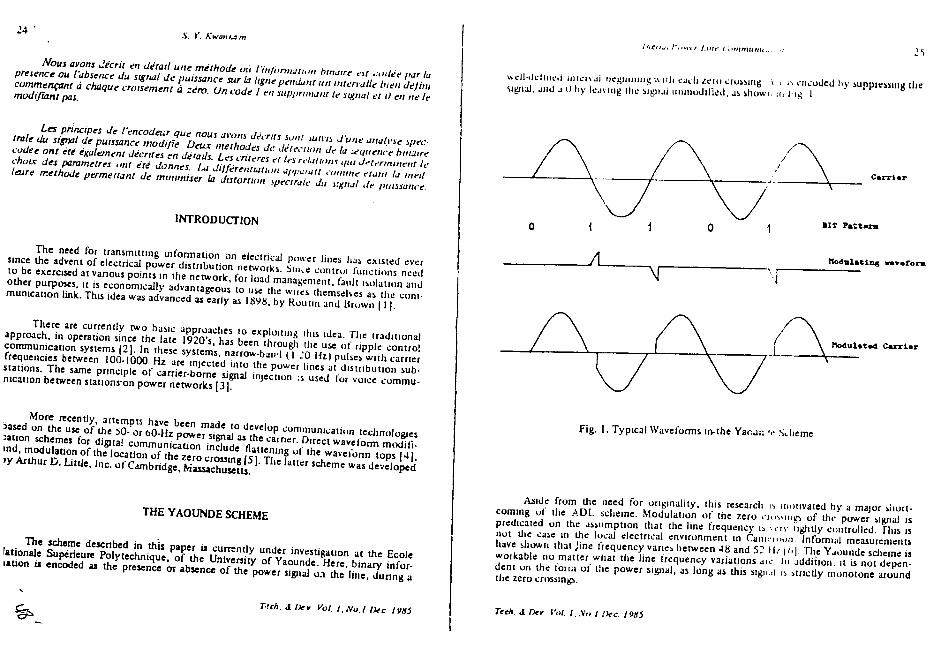


![[PPC 2.0] - Netpeak.ua[PPC 2.0] [PPC 2.0] это уникальный продукт агентства Netpeak [PPC 2.0] = [Контекстная реклама настоящего]](https://img.pdfslide.net/doc/110x75/5ec6c856cbf7fc191035d24f/ppc-20-ppc-20-ppc-20-foe-f-.jpg)