Embed Size (px)
Citation preview

Memory Organization
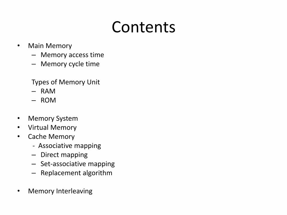
Contents
• Main Memory – Memory access time – Memory cycle time Types of Memory Unit – RAM – ROM
• Memory System • Virtual Memory • Cache Memory - Associative mapping
– Direct mapping – Set-associative mapping – Replacement algorithm
• Memory Interleaving
Main Memory ( 1 )
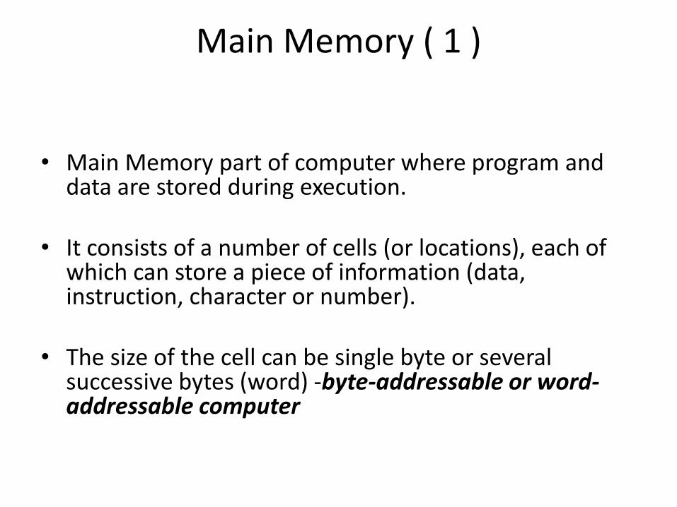
• Main Memory part of computer where program and data are stored during execution.
• It consists of a number of cells (or locations), each of
which can store a piece of information (data, instruction, character or number).
• The size of the cell can be single byte or several
successive bytes (word) -byte-addressable or word-addressable computer
Main Memory ( 2 )
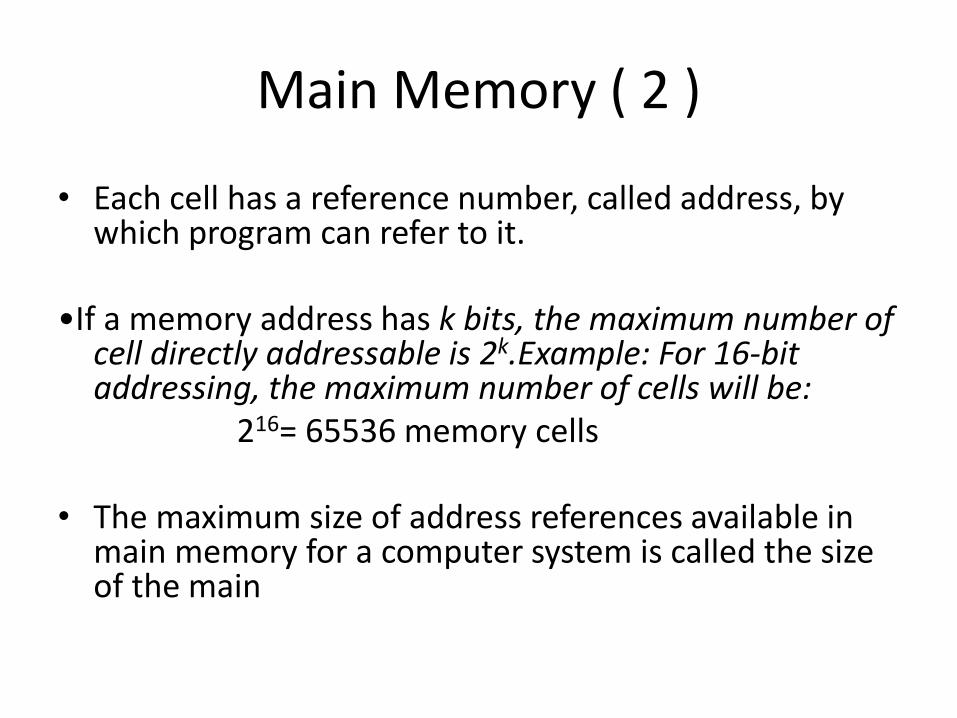
• Each cell has a reference number, called address, by which program can refer to it.
•If a memory address has k bits, the maximum number of
cell directly addressable is 2k.Example: For 16-bit addressing, the maximum number of cells will be:
216= 65536 memory cells • The maximum size of address references available in
main memory for a computer system is called the size of the main
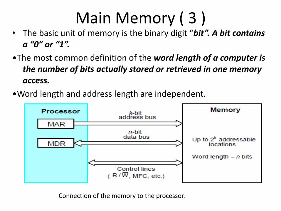
Main Memory ( 3 ) • The basic unit of memory is the binary digit “bit”. A bit contains
a “0” or “1”.
•The most common definition of the word length of a computer is the number of bits actually stored or retrieved in one memory access.
•Word length and address length are independent.
Connection of the memory to the processor.
Main Memory ( 4 )
• Memory Access Time
- The time that elapses between the initiation and the completion of a memory access operation.
- e.g., the time between the READ and MFC signals
• Memory Cycle Time
- The minimum time delay required between two successive memory access operations.
- The cycle time is usually slighter longer than the access time.
Types of Memory Unit ( 1 )
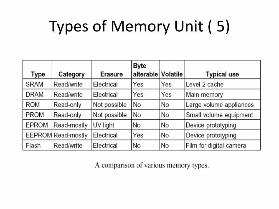
• Random-Access Memory (RAM)
– Any location can be accessed for a Read or Write operation in some constant amount of time that is independent of the memory location.
– Static RAM (SRAM) Memories that consist of circuits capable of
retaining their state as long as power is applied. SRAMs are fast (a few nanoseconds access time) but their cost is
high.
– Dynamic RAM (DRAM)These memory units are capable of storing information for only tens of milliseconds, thus require periodical refresh to maintain the contents.
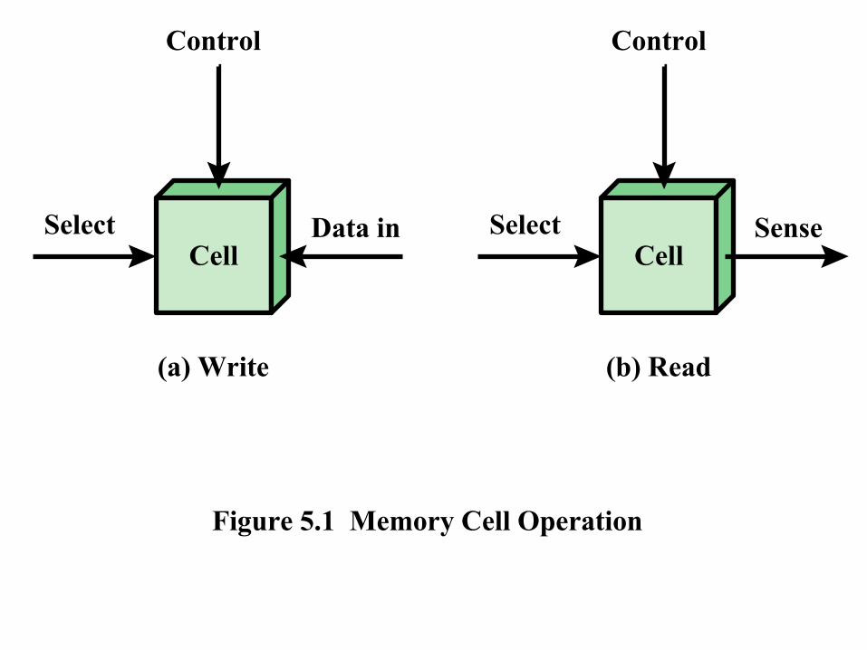
CellSelect Data in
Control
(a) Write
CellSelect Sense
Figure 5.1 Memory Cell Operation
Control
(b) Read
Types of Memory Unit ( 2 )
• Read-Only Memory (ROM) - Nonvolatile memory - Data are written into a ROM when it is manufactured.
Normal operation involves only reading of stored data. - ROM are useful as control store component in a
micro-programmed CPU (micro-coded CPU). - ROM is also commonly used for storing the bootstrap
loader, a program whose function is to load the boot program from the disk into the memory when the power is turn on.
Types of Memory Unit ( 3 )
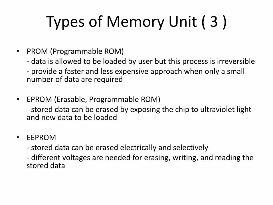
• PROM (Programmable ROM) - data is allowed to be loaded by user but this process is irreversible - provide a faster and less expensive approach when only a small
number of data are required
• EPROM (Erasable, Programmable ROM) - stored data can be erased by exposing the chip to ultraviolet light
and new data to be loaded
• EEPROM - stored data can be erased electrically and selectively - different voltages are needed for erasing, writing, and reading the
stored data
Types of Memory Unit ( 4 )
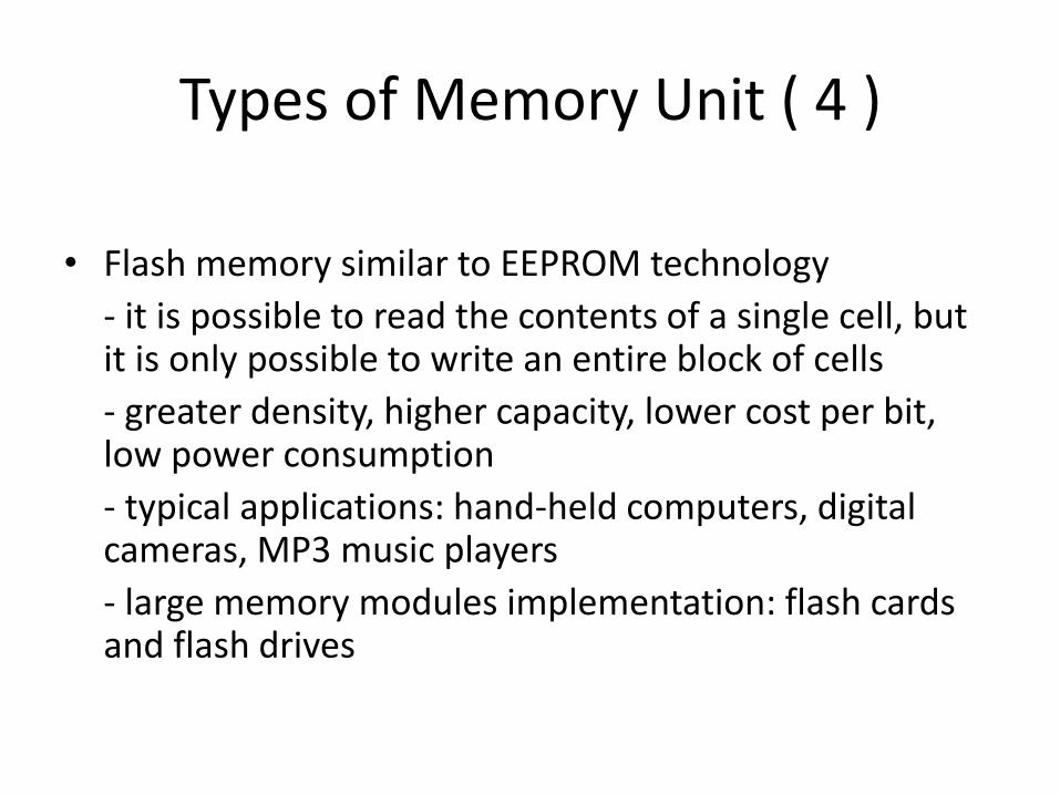
• Flash memory similar to EEPROM technology
- it is possible to read the contents of a single cell, but it is only possible to write an entire block of cells
- greater density, higher capacity, lower cost per bit, low power consumption
- typical applications: hand-held computers, digital cameras, MP3 music players
- large memory modules implementation: flash cards and flash drives
Types of Memory Unit ( 5)
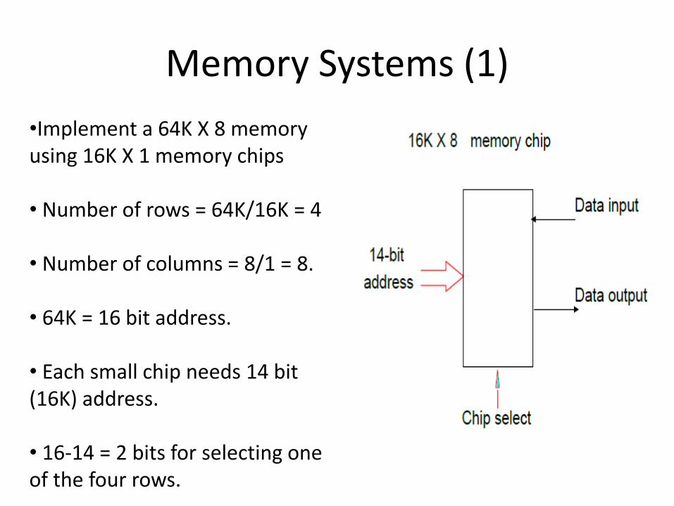
Memory Systems (1) •Implement a 64K X 8 memory using 16K X 1 memory chips • Number of rows = 64K/16K = 4 • Number of columns = 8/1 = 8. • 64K = 16 bit address. • Each small chip needs 14 bit (16K) address. • 16-14 = 2 bits for selecting one of the four rows.
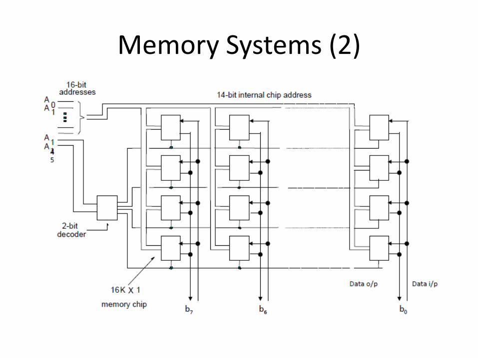
Memory Systems (2)
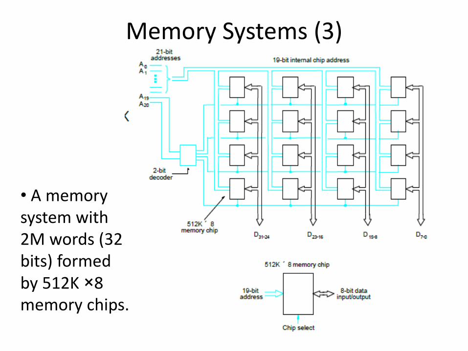
Memory Systems (3)
• A memory system with 2M words (32 bits) formed by 512K ×8 memory chips.
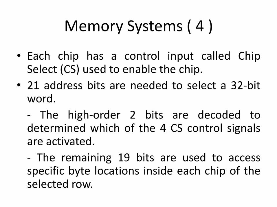
Memory Systems ( 4 )
• Each chip has a control input called Chip Select (CS) used to enable the chip.
• 21 address bits are needed to select a 32-bit word.
- The high-order 2 bits are decoded to determined which of the 4 CS control signals are activated.
- The remaining 19 bits are used to access specific byte locations inside each chip of the selected row.
Memory Systems ( 5 )
• Single In-line Memory Modules (SIMMs) and Dual In-line Memory Modules (DIMMs)
- An assembly of several memory chips on a separate small board that plugs vertically into a single socket on the motherboard
- Occupy a smaller amount of space.
- Allow easy expansion.
+ Cache Addresses
• Virtual memory
– Facility that allows programs to address memory from a logical point of view, without regard to the amount of main memory physically available
– When used, the address fields of machine instructions contain virtual addresses
– For reads to and writes from main memory, a hardware memory management unit (MMU) translates each virtual address into a physical address in main memory
Virtual Memory
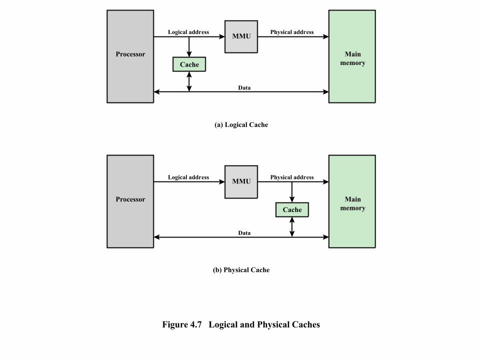
Processor Main
memoryCache
Logical address Physical address
Data
MMU
(a) Logical Cache
Processor Main
memoryCache
Logical address Physical address
Data
MMU
(b) Physical Cache
Figure 4.7 Logical and Physical Caches
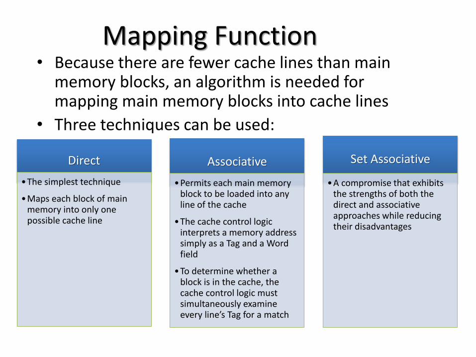
Mapping Function • Because there are fewer cache lines than main
memory blocks, an algorithm is needed for mapping main memory blocks into cache lines
• Three techniques can be used:
Direct
•The simplest technique
•Maps each block of main memory into only one possible cache line
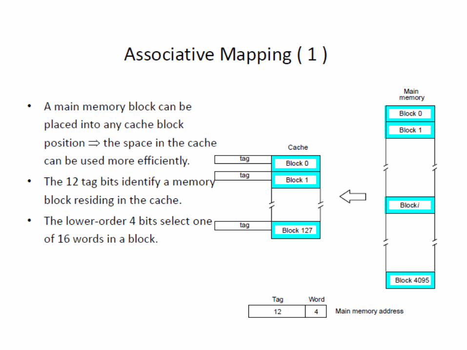
Associative
•Permits each main memory block to be loaded into any line of the cache
•The cache control logic interprets a memory address simply as a Tag and a Word field
•To determine whether a block is in the cache, the cache control logic must simultaneously examine every line’s Tag for a match
Set Associative
•A compromise that exhibits the strengths of both the direct and associative approaches while reducing their disadvantages
Cache Memory ( 1 )
• During the execution of a typical program it is often occurred in a few localized areas of the program (in memory) at any given interval of time –
• Locality of Reference - temporal: a recently executed instructions is likely to
be executed again very soon, e.g., loop, stack. - spatial: instructions in close proximity to a recently
executed instruction are also likely to be executed soon.
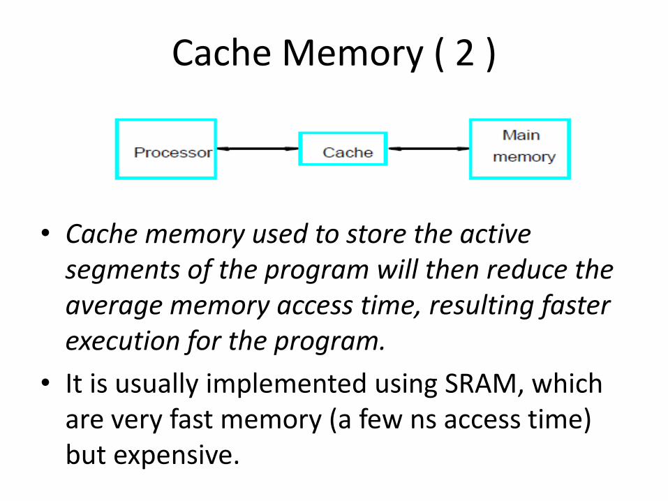
Cache Memory ( 2 )
• Cache memory used to store the active segments of the program will then reduce the average memory access time, resulting faster execution for the program.
• It is usually implemented using SRAM, which are very fast memory (a few ns access time) but expensive.
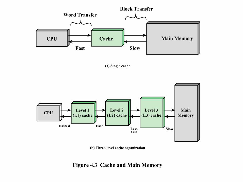
CPU
Word Transfer
Fast
Fastest FastLessfast
Slow
Slow
Block Transfer
Cache Main Memory
Figure 4.3 Cache and Main Memory
(a) Single cache
(b) Three-level cache organization
CPULevel 1
(L1) cache
Level 2
(L2) cache
Level 3
(L3) cache
Main
Memory
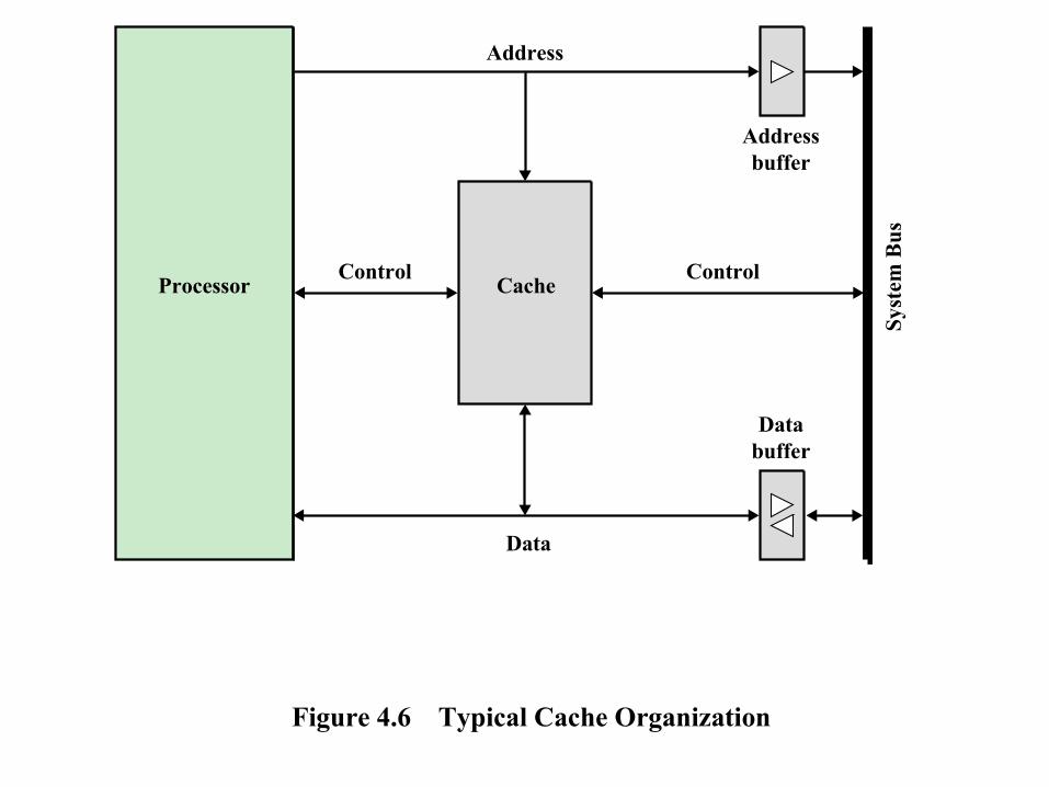
Processor Cache
Address
Address
buffer
Data
buffer
Control
Data
Figure 4.6 Typical Cache Organization
Control
Syst
em B
us
Cache Memory ( 3 )
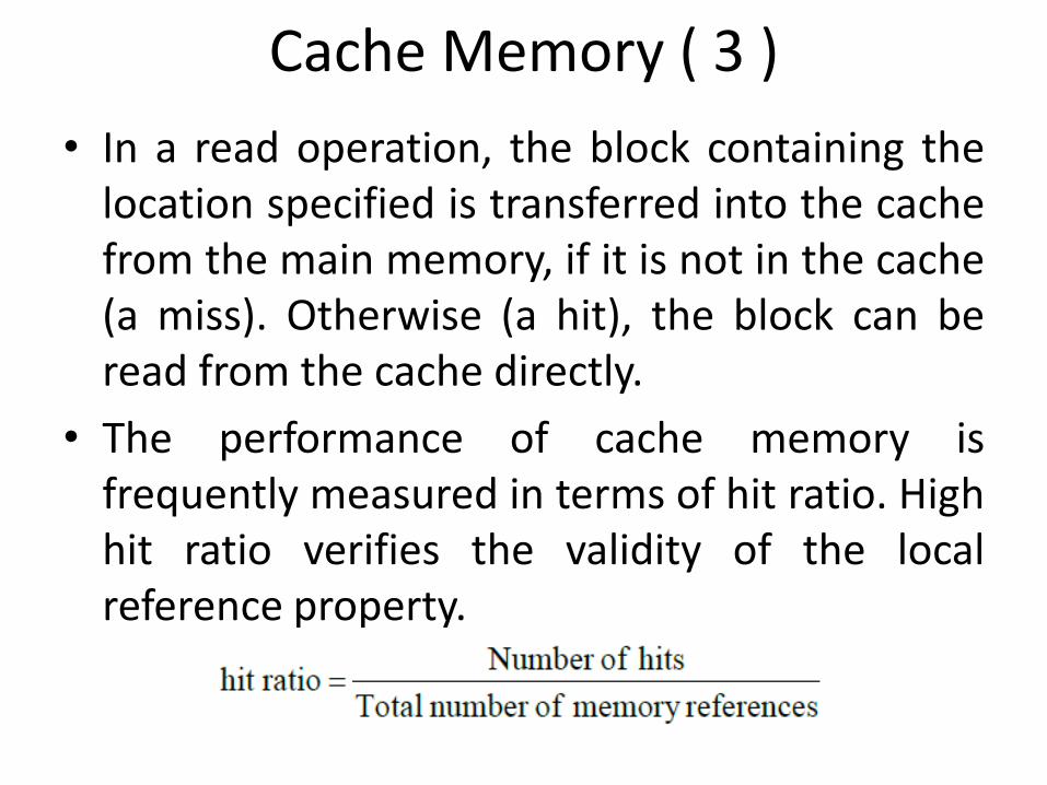
• In a read operation, the block containing the location specified is transferred into the cache from the main memory, if it is not in the cache (a miss). Otherwise (a hit), the block can be read from the cache directly.
• The performance of cache memory is frequently measured in terms of hit ratio. High hit ratio verifies the validity of the local reference property.
Cache Memory ( 4 )
• Two different ways of write access for system with cache memory :
- (1) Write-through method – the cache and the main memory locations are updated simultaneously.
- (2) Write-back method - cache location updated during a write operation is marked with a dirty or modified bit. The main memory location is updated later when the block is to be removed from the cache.
Cache Memory ( 5 )
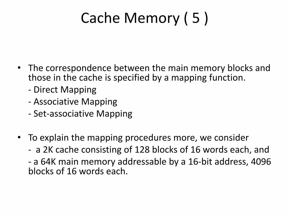
• The correspondence between the main memory blocks and those in the cache is specified by a mapping function.
- Direct Mapping - Associative Mapping - Set-associative Mapping
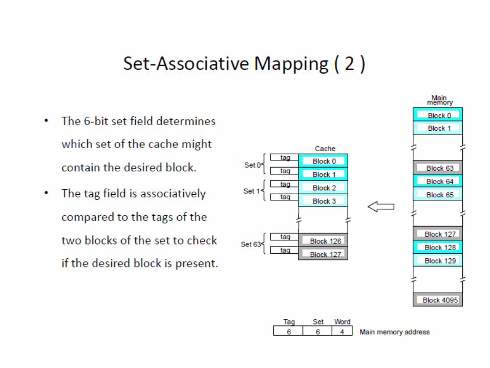
• To explain the mapping procedures more, we consider - a 2K cache consisting of 128 blocks of 16 words each, and - a 64K main memory addressable by a 16-bit address, 4096
blocks of 16 words each.
Direct Mapping ( 1 )
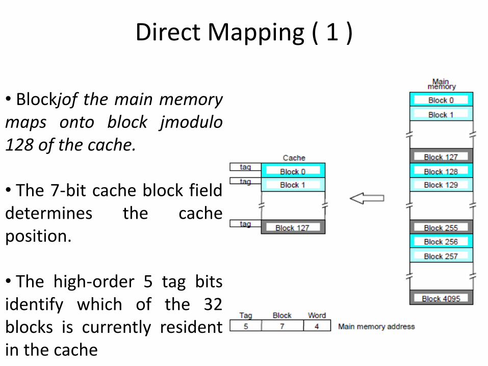
• Blockjof the main memory maps onto block jmodulo 128 of the cache. • The 7-bit cache block field determines the cache position. • The high-order 5 tag bits identify which of the 32 blocks is currently resident in the cache
Direct Mapping ( 2 )
• Since more than one memory block is mapped onto a given cache block position, contention may arise for that position even when the cache is not full
.
• This technique is easy to implement, but it is not flexible.
Associative Mapping ( 2 )
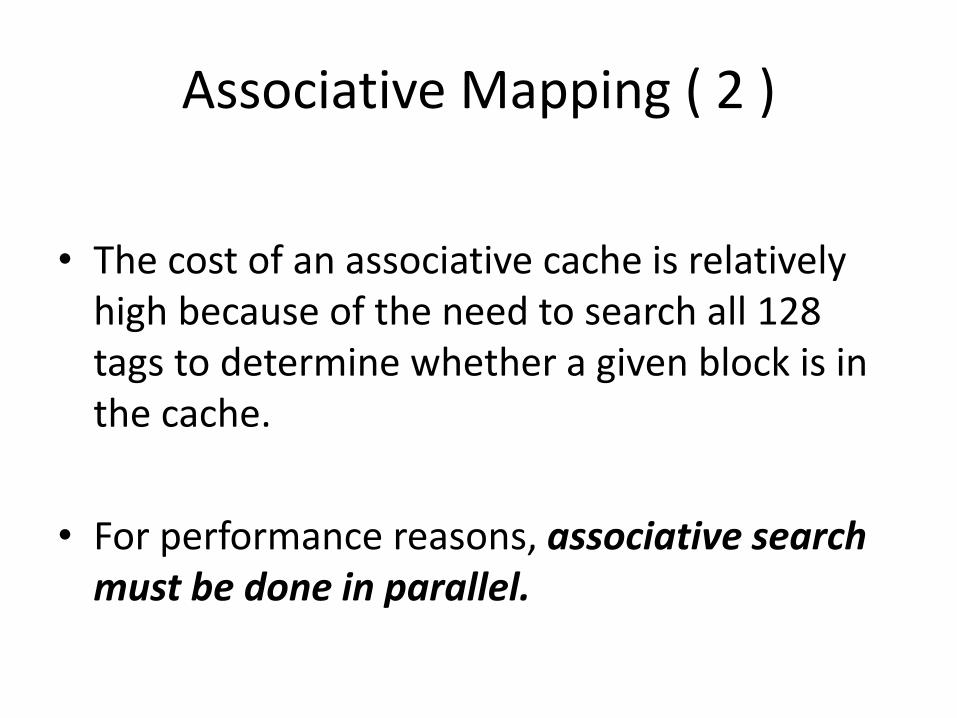
• The cost of an associative cache is relatively high because of the need to search all 128 tags to determine whether a given block is in the cache.
• For performance reasons, associative search must be done in parallel.
Set-Associative Mapping ( 1 )
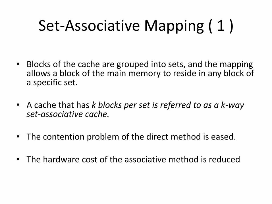
• Blocks of the cache are grouped into sets, and the mapping
allows a block of the main memory to reside in any block of a specific set.
• A cache that has k blocks per set is referred to as a k-way set-associative cache.
• The contention problem of the direct method is eased.
• The hardware cost of the associative method is reduced
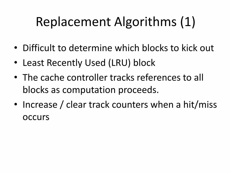
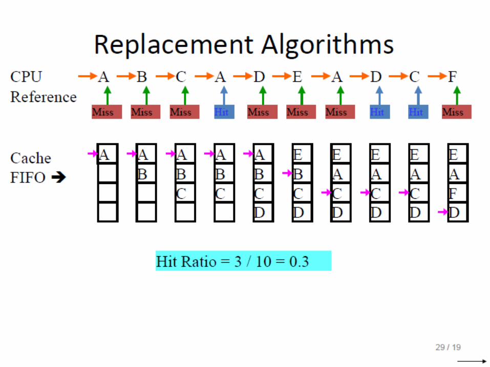
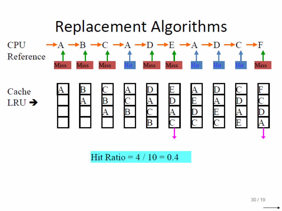
Replacement Algorithms (1)
• Difficult to determine which blocks to kick out
• Least Recently Used (LRU) block
• The cache controller tracks references to all blocks as computation proceeds.
• Increase / clear track counters when a hit/miss occurs
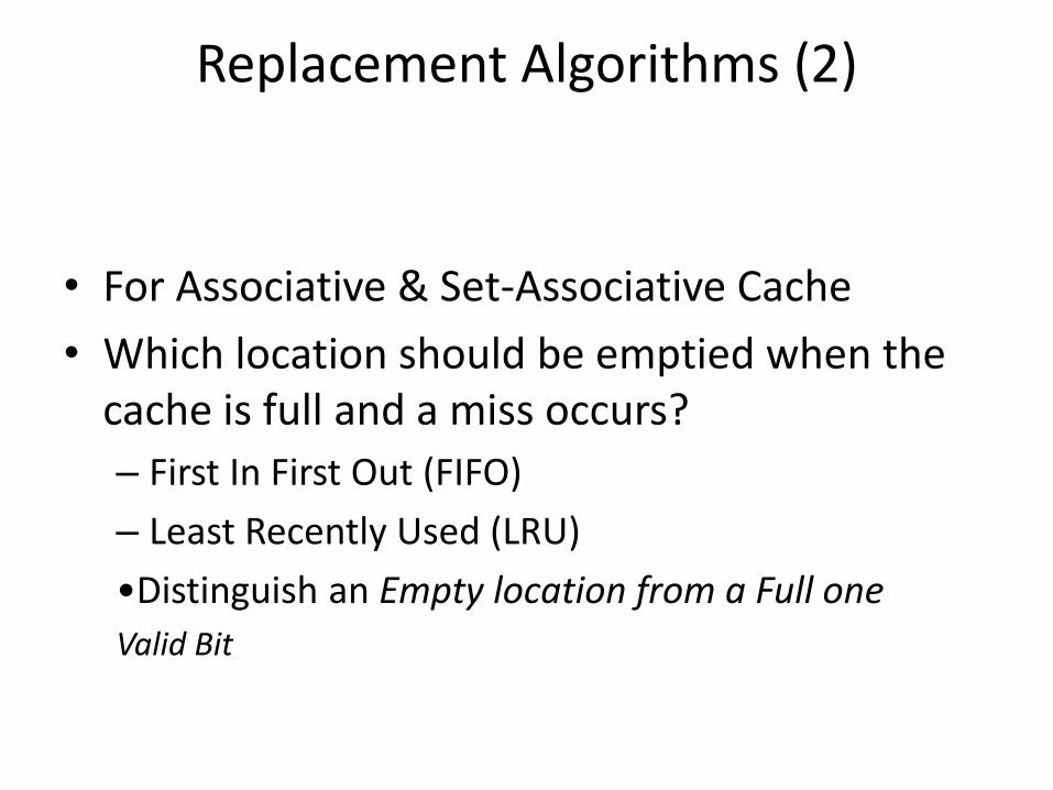
Replacement Algorithms (2)
• For Associative & Set-Associative Cache
• Which location should be emptied when the cache is full and a miss occurs?
– First In First Out (FIFO)
– Least Recently Used (LRU)
•Distinguish an Empty location from a Full one
Valid Bit
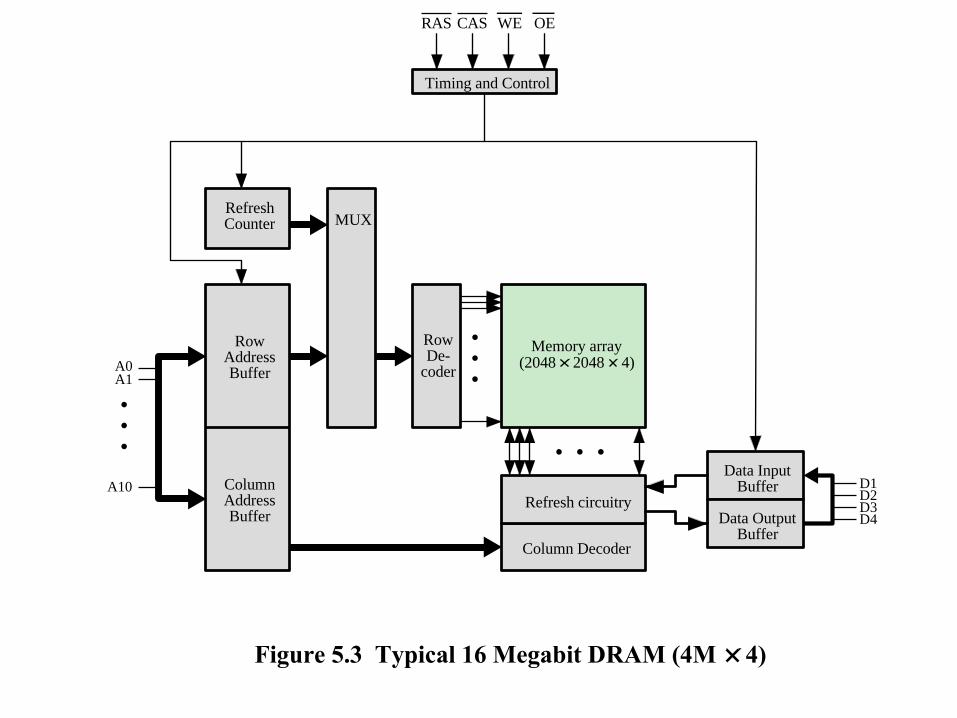
Column Decoder
Refresh circuitry
Memory array(2048 2048 4)
RowDe-
coderA0A1
A10
RowAddressBuffer
ColumnAddressBuffer
Timing and Control
RAS CAS WE OE
MUXRefreshCounter
Data InputBuffer
Data OutputBuffer
D1D2D3D4
Figure 5.3 Typical 16 Megabit DRAM (4M 4)
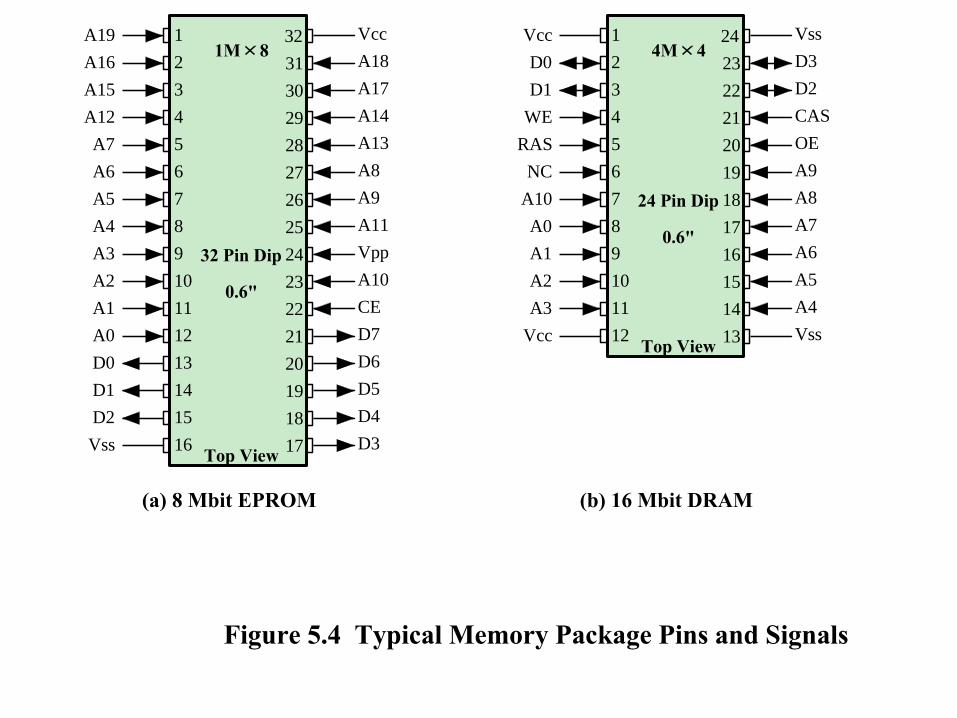
4M 4
24 Pin Dip
0.6"
Top View
Figure 5.4 Typical Memory Package Pins and Signals
32
31
30
29
28
27
26
25
24
23
22
21
20
19
18
17
1
2
3
4
5
6
7
8
9
10
11
12
13
14
15
16
A19
A16
A15
A12
A7
A6
A5
A4
A3
A2
A1
A0
D0
D1
D2
Vss
Vcc
A18
A17
A14
A13
A8
A9
A11
Vpp
A10
CE
D7
D6
D5
D4
D3
32 Pin Dip
0.6"
Top View
1M 824
23
22
21
20
19
18
17
16
15
14
13
1
2
3
4
5
6
7
8
9
10
11
12
Vcc
D0
D1
WE
RAS
NC
A10
A0
A1
A2
A3
Vcc
Vss
D3
D2
CAS
OE
A9
A8
A7
A6
A5
A4
Vss
(a) 8 Mbit EPROM (b) 16 Mbit DRAM
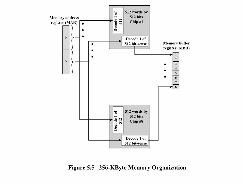
512 words by
512 bits
Chip #1
Memory buffer
register (MBR)
Figure 5.5 256-KByte Memory Organization
Memory address
register (MAR)
Decode 1 of
512 bit-sense
Dec
od
e 1
of
512
512 words by
512 bits
Chip #8
Decode 1 of
512 bit-sense
Dec
od
e 1 o
f
51
2
1
9
92
3
4
5
6
7
8
Memory Interleaving ( 1 )
• Main memory is structured as a number of physical modules (chip).
• Each memory module has its own Address Buffer Register(ABR) and Data Buffer Register(DBR).
• Memory access may proceed in more than one module simultaneously →the aggregate rate of transmission of words to and from the main memory can be increased.
• How individual addresses are distributed over the modules is critical in determining the average number of modules that can be kept busy.
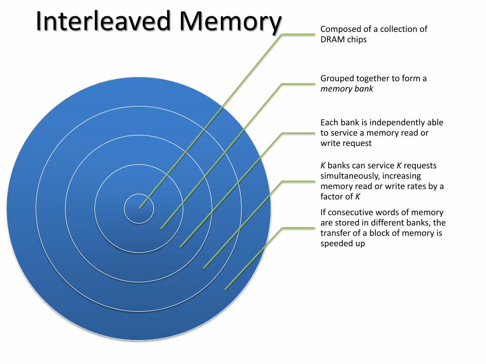
Interleaved Memory Composed of a collection of DRAM chips
Grouped together to form a memory bank
Each bank is independently able to service a memory read or write request
K banks can service K requests simultaneously, increasing memory read or write rates by a factor of K
If consecutive words of memory are stored in different banks, the transfer of a block of memory is speeded up
Memory Interleaving ( 2 )
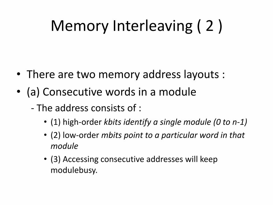
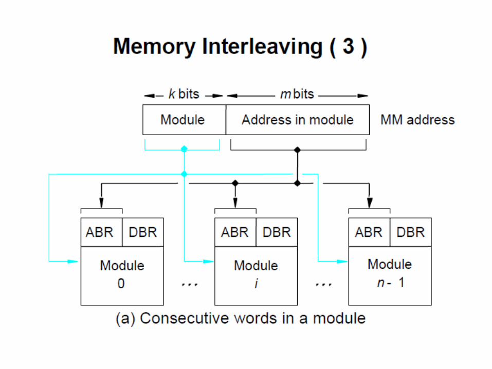
• There are two memory address layouts :
• (a) Consecutive words in a module
- The address consists of :
• (1) high-order kbits identify a single module (0 to n-1)
• (2) low-order mbits point to a particular word in that module
• (3) Accessing consecutive addresses will keep modulebusy.
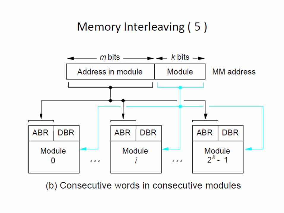
Memory Interleaving ( 4 )
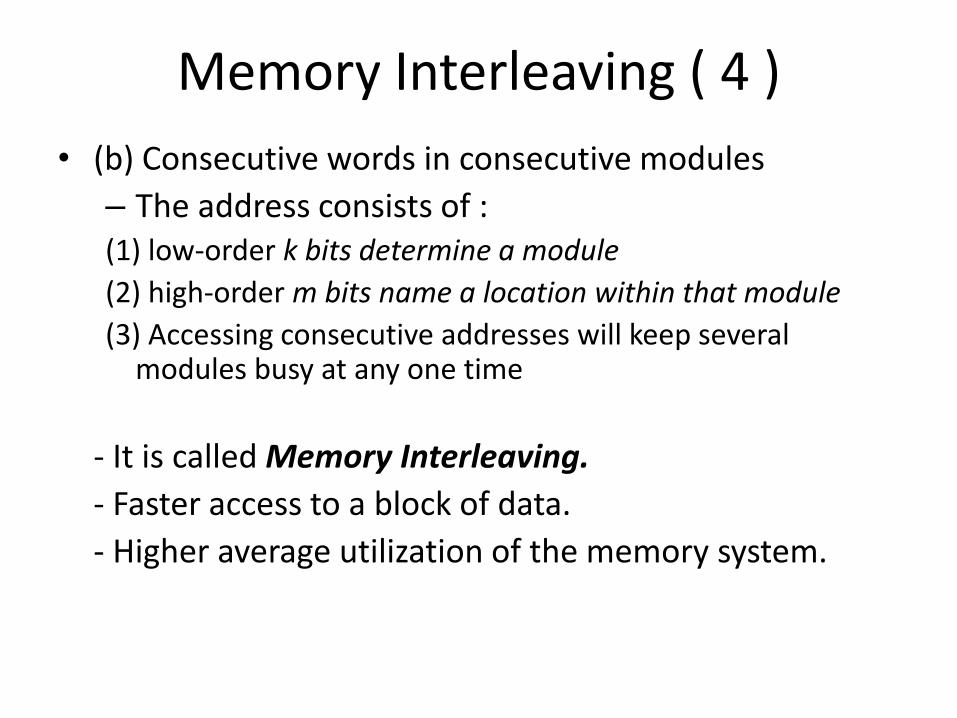
• (b) Consecutive words in consecutive modules
– The address consists of : (1) low-order k bits determine a module
(2) high-order m bits name a location within that module
(3) Accessing consecutive addresses will keep several modules busy at any one time
- It is called Memory Interleaving.
- Faster access to a block of data.
- Higher average utilization of the memory system.
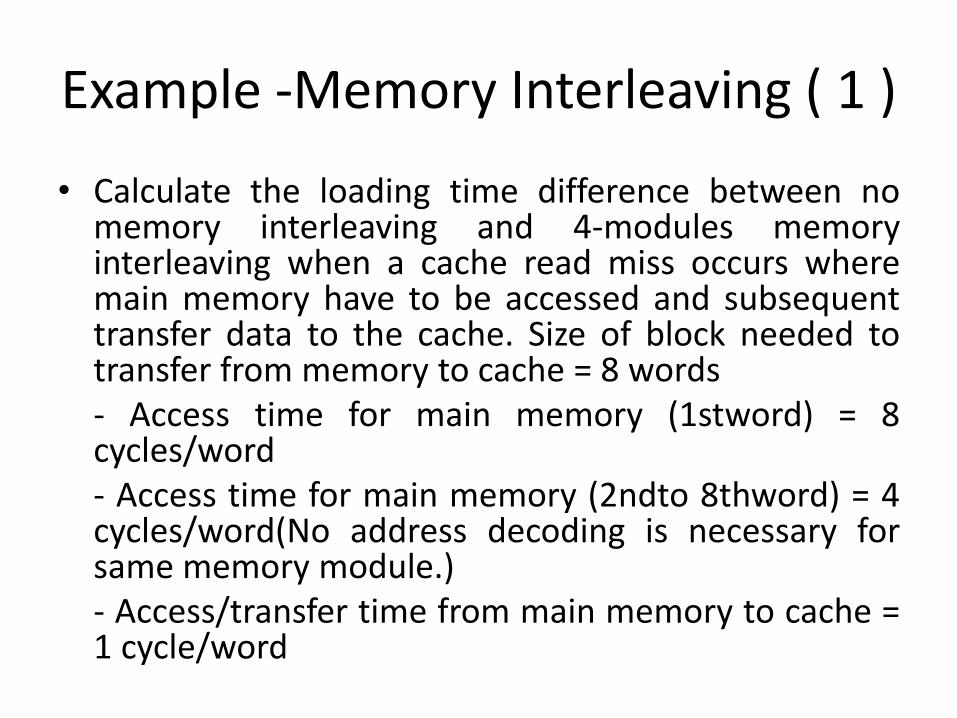
Example -Memory Interleaving ( 1 )
• Calculate the loading time difference between no memory interleaving and 4-modules memory interleaving when a cache read miss occurs where main memory have to be accessed and subsequent transfer data to the cache. Size of block needed to transfer from memory to cache = 8 words
- Access time for main memory (1stword) = 8 cycles/word
- Access time for main memory (2ndto 8thword) = 4 cycles/word(No address decoding is necessary for same memory module.)
- Access/transfer time from main memory to cache = 1 cycle/word
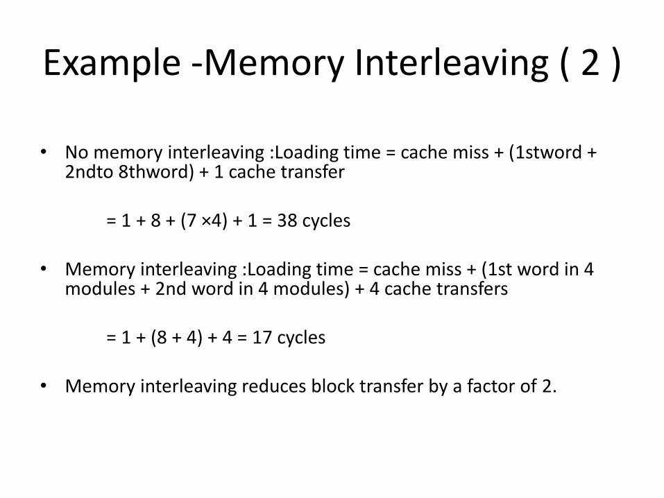
Example -Memory Interleaving ( 2 )
• No memory interleaving :Loading time = cache miss + (1stword +
2ndto 8thword) + 1 cache transfer
= 1 + 8 + (7 ×4) + 1 = 38 cycles • Memory interleaving :Loading time = cache miss + (1st word in 4
modules + 2nd word in 4 modules) + 4 cache transfers
= 1 + (8 + 4) + 4 = 17 cycles • Memory interleaving reduces block transfer by a factor of 2.