Embed Size (px)
Citation preview

NFDML
Memory Types & Hierarchy
Requirements of memory device
• Fast Write / Read Speed
• High Write / Read Throughput
• Random Access
• Non-volatility
• Low Power Consumption
• Low Cost / High Density
Data
Storage
Inside
CPU
SSD
SRAM : Speed
DRAM : Speed/Cost
NAND : Cost
Memory types
and strong points
Semiconductor
Memory
Single memory type cannot cover
all the requirements
source : www.ts.avnet.com

NFDML
Memory performance comparison chart
Volatility Volatile Non-Volatile
SRAM DRAM NAND FeRAM MRAM PRAM ReRAM
Cell Size(F2) 150~200 ~8 2 30~8020~40 (a)
~8 (b)
~4
2 (3D stack) 2
Read Time ~1ns ~30ns ~50us ~70ns < 30ns ~30ns 30ns~1us
Write Time ~1ns ~30ns ~1ms ~70ns < 30ns ~500ns 30ns~1us
Endurance > 1015 > 1015 105 1012 > 1015 107 > 107
Byte Operation O O X O O O O
Commercialized -1970
Intel
1989
Toshiba
2006
Fujizsu /
Ramtron
2006 (a)
Freescale
2010
Samsung
2015
Intel / Micron
Under
Research
(a) : Field Switching MRAM
(b) : STT-MRAM
Each memory has its own strength
Cannot be easily replaced by others

NFDML
Classification - Operating principles
Capacitor Based Resistor Based
Data “1” Data “0” Data “1” Data “0”
Current Flow
• DRAM
• SRAM
• Flash
Difficult to increase memory density
(scaling device size)
- Capacitance (Bottle volume) ↓
Signal strength ↓
• PRAM (Phase-change Memory)
• MRAM (Magnetic Memory)
• RRAM (Resistive Memory)
Advantages to increasing density
- Signal strength is insensitive to
device size

NFDML
Classification
Volatile Non-Volatile
Cap
ac
ito
r B
as
ed
Res
isto
r B
as
ed
Magnet Tunneling oxide
“0”
“1”
R
H
PRAM MRAM RRAM
•Top Electrode
ContactPhase Change
Region
Heater
GST
“0”
“1”
CurrentI
V
Electrode Metal oxide
“1”
I
V
“0”
DRAM SRAM FLASH

NFDML
DRAM
Bit Line
Wo
rd L
ine
Capacitor
Gate
Unit Cell
D S
1 Transistor + 1 Capacitor
CapacitorThe location where charge is stored.
Composed of Storage Node,
Dielectric, and Plate node triple
structure.
Cap
acit
or
Bit Line
Word Line
S D S
S : Source
D : Drain
Charged capacitor representing data ‘1’ and an uncharged capacitor ‘0’
Bit LineData I/O line
Cell Transistor + Word LineTransferring charge between
capacitor and bit line to store / read
data

NFDML
DRAM – evolution of capacitor
200nm
Stack+HSG Cylinder
+HSG
Cylinder S-OCS StackStack
50nm100nm
SiO2 / Si3N4 Al2O3, Ta2O5, HfO2 HfO2, ZrO2, SrTiO3
* HSG : Hemi-Spherical Grain
Low-k & Complex Structure High-k & Simple Structure

NFDML
Flash
Erase Program
Use F-N tunneling to ‘trap’ electron at
Floating Gate
Si Sub.
FGCG
Fowler–
Nordheim
tunneling
0V
20V

NFDML
Flash – nowadays2D NAND 3D NAND
Floating Poly Gate Charge Trap Flash (CTF) Technology
n+
n+n+
Control
Gate
(W/L)
GSL Gate
SSL Gate
p-Sub
CG
(WL)
Trap
(ONO)
Channel
(Poly)
CG
FG
2D NAND 3D NAND
• Bit growth : Cell dimension decreased by 3D stacking Overcomes scaling issue
• High program performance : Decreased interference between cells
• Low power consumption
Widen the gap by structure change
source : samsungsemiconstory.com

NFDML
PcRAM (Phase-change RAM)
BEC
Crystalline
Top Electrode
Bottom Electrode
Low resistance
SET state : “0”
High resistance
RESET state : “1”
BEC
Top Electrode
Bottom Electrode
Amorphous
TEC
TE
BEC
CrystallineCrystalline
Amorphous
Reversible phase change of
chalcogenide material
( Crystalline Amorphous)
• Writing : Current heating
• Reading : Resistance change

NFDML
Switching Behavior of PRAM
0.
0
0.2 0.4 0.6 0.8 1.0 1.2 1.410
2
103
104
105
106
107
Set
Reset
Re
sis
tan
ce (
Oh
m)
I/Ireset
TEC
TE
BEC
CrystallineCrystalline
Amorphous
0 100 200 300 400 50010
1
102
103
104
105
106
107
108
To
tal F
ail B
itPulse Width (nsec)
Reset (Set = 500 ns)
Set (Reset = 50 ns)
Set/Reset Transition Switching Speed
G. H. Koh, ISADPT(2003)
• Switching speed Crystallization limit
(transition to SET)
• Switching current Melting limit
(transition to RESET)

NFDML
PRAM – 3D Stack
Cross-point cell structure
– Cell selector : OTS (Ovonic Threshold switching)
– Cell storage : PCM (Phase change memory )
D. Kau, Intel/Numonyx, IEDM 2009
Challenges :
- Selector technology
- Process integration & characteristic distribution control

NFDML
PRAM - nowadays
3D-Xpoint Memory - Intel/Micron (2015)

NFDML
PRAM – 3D VNAND-like Cell Structure
• Vertical Poly-Si Tr + Phase change material
• Thin channel Tr, Thin PCM Memory hole size scaling
( NAND 60nm VCCPM 32nm )
• Vertical poly-Si diode : String Selector. Cell dimension 6F2 (Tr) 4F2 (diode)
M. Kinoshita, Hitachi, VLSI 201

NFDML
MRAM (Magnetic RAM)
WL
BL
MTJ MTJ
WL
BL SL
MTJ (Magnetic Tunnel Junction)
: Spin-dependent tunneling
: Resistance change controlled by magnetization direction
Parallel Magnetization
Low Resistance (Rp)
Read
Current
Anti-Parallel Magnetization
High Resistance (Rap)
Tunneling oxide
Ferromagnetic electrode
(Free layer)
Ferromagnetic electrode
(Pinned layer)
P
PAP
R
RRTMR
TMR : Tunneling Magneto-resistance

NFDML
MRAM – Types and charateristics
Field -MRAMSTT-MRAM
(in-plane mag.)
STT-MRAM
(out-of-plane mag.)
Operation
Principle
Characteristic
- MTJ size decrease
→ Isw increase
- Disturb issue in half-
selected cells
- MTJ size decrease
→ Isw decrease
- MTJ aspect ratio > 2:1
- MTJ size decrease
→ Isw decrease
- MTJ aspect ratio ~ 1:1
Cell Area > 22.5F2 6~12F2 4~12F2
AnisotropyShape
Ku~104 erg/cc
Shape
Ku~104 erg/cc
Interface
Ku~5*106 erg/cc
Bulk
Ku~107 erg/cc
Scalability
Limit~ 90nm 30 ~ 40nm 10~20nm 5~10nm
W/L
D/L
B/LB/L
MTJ
S/L
MTJ
B/L
W/L
e
S/L
MTJ
B/L
W/L
e
Field Switching STT Switching STT Switching

NFDML
RRAM (Resistive RAM)
R. Waser, Nature Materials 2007
RRAM : R depends on the state of the film
Low Resistance (SET) & High resistance (RESET)
- Unipolar : SET & RESET switching occurs
at the same polarity
- Bipolar : SET & RESET switching occurs
at opposite polarity
NFDML
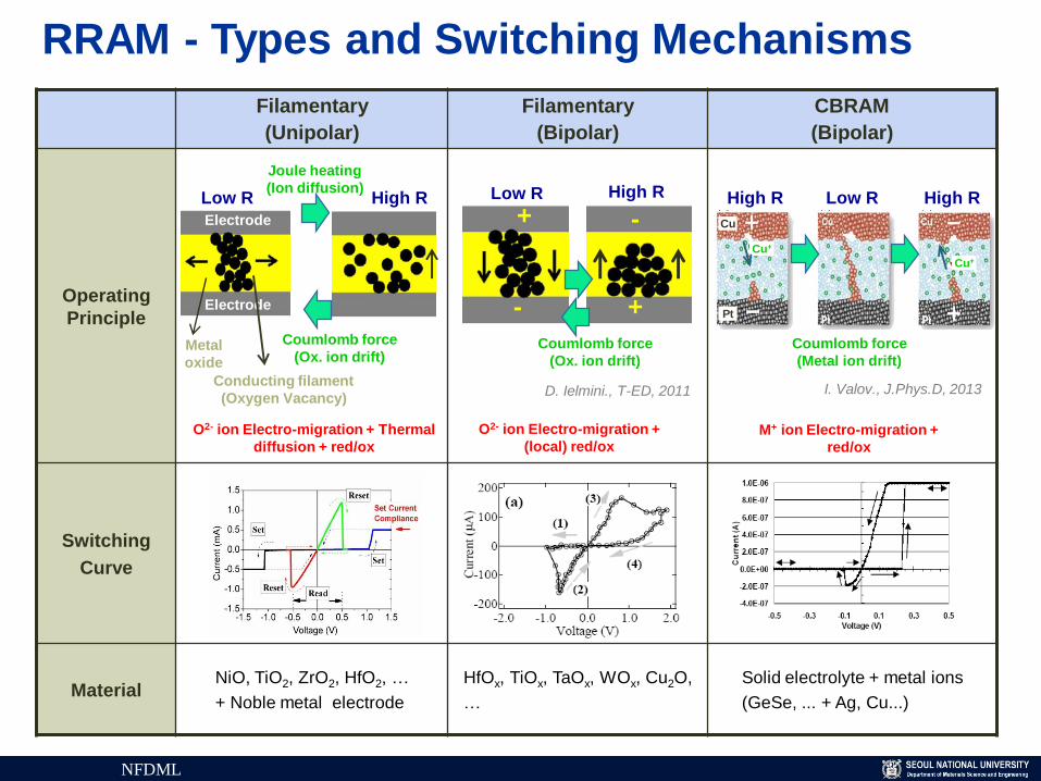
RRAM - Types and Switching Mechanisms
Filamentary
(Unipolar)
Filamentary
(Bipolar)
CBRAM
(Bipolar)
Operating
Principle
Switching
Curve
MaterialNiO, TiO2, ZrO2, HfO2, …
+ Noble metal electrode
HfOx, TiOx, TaOx, WOx, Cu2O,
…
Solid electrolyte + metal ions
(GeSe, ... + Ag, Cu...)
I. Valov., J.Phys.D, 2013
O2- ion Electro-migration + Thermal
diffusion + red/ox
O2- ion Electro-migration +
(local) red/oxM+ ion Electro-migration +
red/ox
Metal
oxide
Electrode
Electrode
Conducting filament
(Oxygen Vacancy)
Low R High R
Joule heating
(Ion diffusion)
Coumlomb force
(Ox. ion drift)
Low R High R
Coumlomb force
(Ox. ion drift)
+
-
-
+
Low RHigh R High R
Coumlomb force
(Metal ion drift)
Cu
Pt
Cu+
Cu+
D. Ielmini., T-ED, 2011