Embed Size (px)
Citation preview

January 2008 Rev 2 1/48
48
LIS3LV02DLMEMS inertial sensor
3-axis - ±2g/±6g digital output low voltage linear accelerometer
Features■ 2.16 V to 3.6 V single supply operation
■ 1.8 V compatible IOs
■ I2C/SPI digital output interfaces
■ Programmable 12 or 16 bit data representation
■ Interrupt activated by motion
■ Programmable interrupt threshold
■ Embedded self test
■ High shock survivability
■ ECOPACK® compliant (see Section 9)
DescriptionThe LIS3LV02DL is a three axes digital output linear accelerometer that includes a sensing element and an IC interface able to take the information from the sensing element and to provide the measured acceleration signals to the external world through an I2C/SPI serial interface.
The sensing element, capable of detecting the acceleration, is manufactured using a dedicated process developed by ST to produce inertial sensors and actuators in silicon.
The IC interface instead is manufactured using a CMOS process that allows high level of integration to design a dedicated circuit which is factory trimmed to better match the sensing element characteristics.
The LIS3LV02DL has a user selectable full scale of ±2g, ±6g and it is capable of measuring acceleration over a bandwidth of 640 Hz for all axes. The device bandwidth may be selected accordingly to the application requirements.
The self-test capability allows the user to check the functioning of the device.
The device may be also configured to generate an inertial wake-up/free-fall interrupt signal when a programmable acceleration threshold is crossed at least in one of the three axes.
The LIS3LV02DL is available in plastic SMD package and it is specified over a temperature range extending from -40°C to +85°C.
The LIS3LV02DL belongs to a family of products suitable for a variety of applications:
– Free-Fall detection– Motion activated functions in portable
terminals– Antitheft systems and Inertial navigation– Gaming and virtual reality input devices– Vibration monitoring and compensation
LGA-16
Table 1. Device summary
Order codeOperating temperature
range [° C]Package Packing
LIS3LV02DL -40 to +85 LGA-16 Tray
LIS3LV02DLTR -40 to +85 LGA-16 Tape and reel
www.st.com

Content LIS3LV02DL
2/48
Content
1 Block diagram and pin description . . . . . . . . . . . . . . . . . . . . . . . . . . . . . 8
1.1 Block diagram . . . . . . . . . . . . . . . . . . . . . . . . . . . . . . . . . . . . . . . . . . . . . . . 8
1.2 LGA-16 pin description . . . . . . . . . . . . . . . . . . . . . . . . . . . . . . . . . . . . . . . . 8
2 Mechanical and electrical specifications . . . . . . . . . . . . . . . . . . . . . . . 10
2.1 Mechanical characteristics . . . . . . . . . . . . . . . . . . . . . . . . . . . . . . . . . . . . 10
2.2 Electrical characteristics . . . . . . . . . . . . . . . . . . . . . . . . . . . . . . . . . . . . . . 14
2.3 Communication interface characteristics . . . . . . . . . . . . . . . . . . . . . . . . . 15
2.3.1 SPI - serial peripheral interface . . . . . . . . . . . . . . . . . . . . . . . . . . . . . . . 15
2.3.2 I2C - Inter IC control interface . . . . . . . . . . . . . . . . . . . . . . . . . . . . . . . . 16
2.4 Absolute maximum ratings . . . . . . . . . . . . . . . . . . . . . . . . . . . . . . . . . . . . 17
2.5 Terminology . . . . . . . . . . . . . . . . . . . . . . . . . . . . . . . . . . . . . . . . . . . . . . . 18
2.5.1 Sensitivity . . . . . . . . . . . . . . . . . . . . . . . . . . . . . . . . . . . . . . . . . . . . . . . . 18
2.5.2 Zero-g level . . . . . . . . . . . . . . . . . . . . . . . . . . . . . . . . . . . . . . . . . . . . . . 18
2.5.3 Self test . . . . . . . . . . . . . . . . . . . . . . . . . . . . . . . . . . . . . . . . . . . . . . . . . 18
3 Functionality . . . . . . . . . . . . . . . . . . . . . . . . . . . . . . . . . . . . . . . . . . . . . . 19
3.1 Sensing element . . . . . . . . . . . . . . . . . . . . . . . . . . . . . . . . . . . . . . . . . . . . 19
3.2 IC interface . . . . . . . . . . . . . . . . . . . . . . . . . . . . . . . . . . . . . . . . . . . . . . . . 19
3.3 Factory calibration . . . . . . . . . . . . . . . . . . . . . . . . . . . . . . . . . . . . . . . . . . 20
4 Application hints . . . . . . . . . . . . . . . . . . . . . . . . . . . . . . . . . . . . . . . . . . . 21
4.1 Soldering Information . . . . . . . . . . . . . . . . . . . . . . . . . . . . . . . . . . . . . . . . 21
5 Digital interfaces . . . . . . . . . . . . . . . . . . . . . . . . . . . . . . . . . . . . . . . . . . . 22
5.1 I2C serial interface . . . . . . . . . . . . . . . . . . . . . . . . . . . . . . . . . . . . . . . . . . 22
5.1.1 I2C operation . . . . . . . . . . . . . . . . . . . . . . . . . . . . . . . . . . . . . . . . . . . . . 23
5.2 SPI bus interface . . . . . . . . . . . . . . . . . . . . . . . . . . . . . . . . . . . . . . . . . . . 24
5.2.1 SPI read . . . . . . . . . . . . . . . . . . . . . . . . . . . . . . . . . . . . . . . . . . . . . . . . . 25
5.2.2 SPI write . . . . . . . . . . . . . . . . . . . . . . . . . . . . . . . . . . . . . . . . . . . . . . . . 26
5.2.3 SPI Read in 3-wires mode . . . . . . . . . . . . . . . . . . . . . . . . . . . . . . . . . . . 27
6 Register mapping . . . . . . . . . . . . . . . . . . . . . . . . . . . . . . . . . . . . . . . . . . 28

LIS3LV02DL Content
3/48
7 Register description . . . . . . . . . . . . . . . . . . . . . . . . . . . . . . . . . . . . . . . . 30
7.1 WHO_AM_I (0Fh) . . . . . . . . . . . . . . . . . . . . . . . . . . . . . . . . . . . . . . . . . . . 30
7.2 OFFSET_X (16h) . . . . . . . . . . . . . . . . . . . . . . . . . . . . . . . . . . . . . . . . . . . 30
7.3 OFFSET_Y (17h) . . . . . . . . . . . . . . . . . . . . . . . . . . . . . . . . . . . . . . . . . . . 30
7.4 OFFSET_Z (18h) . . . . . . . . . . . . . . . . . . . . . . . . . . . . . . . . . . . . . . . . . . . 30
7.5 GAIN_X (19h) . . . . . . . . . . . . . . . . . . . . . . . . . . . . . . . . . . . . . . . . . . . . . . 31
7.6 GAIN_Y (1Ah) . . . . . . . . . . . . . . . . . . . . . . . . . . . . . . . . . . . . . . . . . . . . . 31
7.7 GAIN_Z (1Bh) . . . . . . . . . . . . . . . . . . . . . . . . . . . . . . . . . . . . . . . . . . . . . . 31
7.8 CTRL_REG1 (20h) . . . . . . . . . . . . . . . . . . . . . . . . . . . . . . . . . . . . . . . . . . 31
7.9 CTRL_REG2 (21h) . . . . . . . . . . . . . . . . . . . . . . . . . . . . . . . . . . . . . . . . . . 32
7.10 CTRL_REG3 (22h) . . . . . . . . . . . . . . . . . . . . . . . . . . . . . . . . . . . . . . . . . . 34
7.11 HP_FILTER_RESET (23h) . . . . . . . . . . . . . . . . . . . . . . . . . . . . . . . . . . . . 34
7.12 STATUS_REG (27h) . . . . . . . . . . . . . . . . . . . . . . . . . . . . . . . . . . . . . . . . . 34
7.13 OUTX_L (28h) . . . . . . . . . . . . . . . . . . . . . . . . . . . . . . . . . . . . . . . . . . . . . 35
7.14 OUTX_H (29h) . . . . . . . . . . . . . . . . . . . . . . . . . . . . . . . . . . . . . . . . . . . . . 35
7.15 OUTY_L (2Ah) . . . . . . . . . . . . . . . . . . . . . . . . . . . . . . . . . . . . . . . . . . . . . 35
7.16 OUTY_H (2Bh) . . . . . . . . . . . . . . . . . . . . . . . . . . . . . . . . . . . . . . . . . . . . . 36
7.17 OUTZ_L (2Ch) . . . . . . . . . . . . . . . . . . . . . . . . . . . . . . . . . . . . . . . . . . . . . 36
7.18 OUTZ_H (2Dh) . . . . . . . . . . . . . . . . . . . . . . . . . . . . . . . . . . . . . . . . . . . . . 36
7.19 FF_WU_CFG (30h) . . . . . . . . . . . . . . . . . . . . . . . . . . . . . . . . . . . . . . . . . 37
7.20 FF_WU_SRC (31h) . . . . . . . . . . . . . . . . . . . . . . . . . . . . . . . . . . . . . . . . . 37
7.21 FF_WU_ACK (32h) . . . . . . . . . . . . . . . . . . . . . . . . . . . . . . . . . . . . . . . . . 38
7.22 FF_WU_THS_L (34h) . . . . . . . . . . . . . . . . . . . . . . . . . . . . . . . . . . . . . . . 38
7.23 FF_WU_THS_H (35h) . . . . . . . . . . . . . . . . . . . . . . . . . . . . . . . . . . . . . . . 38
7.24 FF_WU_DURATION (36h) . . . . . . . . . . . . . . . . . . . . . . . . . . . . . . . . . . . . 39
7.25 DD_CFG (38h) . . . . . . . . . . . . . . . . . . . . . . . . . . . . . . . . . . . . . . . . . . . . . 39
7.26 DD_SRC (39h) . . . . . . . . . . . . . . . . . . . . . . . . . . . . . . . . . . . . . . . . . . . . . 40
7.27 DD_ACK (3Ah) . . . . . . . . . . . . . . . . . . . . . . . . . . . . . . . . . . . . . . . . . . . . . 41
7.28 DD_THSI_L (3Ch) . . . . . . . . . . . . . . . . . . . . . . . . . . . . . . . . . . . . . . . . . . 41
7.29 DD_THSI_H (3Dh) . . . . . . . . . . . . . . . . . . . . . . . . . . . . . . . . . . . . . . . . . . 41
7.30 DD_THSE_L (3Eh) . . . . . . . . . . . . . . . . . . . . . . . . . . . . . . . . . . . . . . . . . . 41
7.31 DD_THSE_H (3Fh) . . . . . . . . . . . . . . . . . . . . . . . . . . . . . . . . . . . . . . . . . 41

Content LIS3LV02DL
4/48
8 Typical performance characteristics . . . . . . . . . . . . . . . . . . . . . . . . . . . 42
8.1 Mechanical characteristics at 25°C . . . . . . . . . . . . . . . . . . . . . . . . . . . . . 42
8.2 Mechanical characteristics derived from measurement in the -40°C to +85°C temperature range . . . . . . . . . . . . . . . . . . . . . . . . . . . . . . . . . . . . . . . . . . 43
8.3 Electro-mechanical characteristics at 25°C . . . . . . . . . . . . . . . . . . . . . . . 44
9 Package information . . . . . . . . . . . . . . . . . . . . . . . . . . . . . . . . . . . . . . . . 46
10 Revision history . . . . . . . . . . . . . . . . . . . . . . . . . . . . . . . . . . . . . . . . . . . 47

LIS3LV02DL List of figures
5/48
List of figures
Figure 1. Block diagram . . . . . . . . . . . . . . . . . . . . . . . . . . . . . . . . . . . . . . . . . . . . . . . . . . . . . . . . . . . . 5Figure 2. Pin connection . . . . . . . . . . . . . . . . . . . . . . . . . . . . . . . . . . . . . . . . . . . . . . . . . . . . . . . . . . . 5Figure 3. SPI slave timing diagram . . . . . . . . . . . . . . . . . . . . . . . . . . . . . . . . . . . . . . . . . . . . . . . . . . 12Figure 5. LIS3LV02DL electrical connection . . . . . . . . . . . . . . . . . . . . . . . . . . . . . . . . . . . . . . . . . . . 18Figure 6. Read and write protocol . . . . . . . . . . . . . . . . . . . . . . . . . . . . . . . . . . . . . . . . . . . . . . . . . . . 21Figure 7. SPI read protocol . . . . . . . . . . . . . . . . . . . . . . . . . . . . . . . . . . . . . . . . . . . . . . . . . . . . . . . . 22Figure 8. Multiple bytes SPI read protocol (2 bytes example) . . . . . . . . . . . . . . . . . . . . . . . . . . . . . . 23Figure 9. SPI write protocol . . . . . . . . . . . . . . . . . . . . . . . . . . . . . . . . . . . . . . . . . . . . . . . . . . . . . . . . 23Figure 10. Multiple bytes SPI write protocol (2 bytes example) . . . . . . . . . . . . . . . . . . . . . . . . . . . . . . 23Figure 11. SPI read protocol in 3-wires mode . . . . . . . . . . . . . . . . . . . . . . . . . . . . . . . . . . . . . . . . . . . 24Figure 12. X-axis zero-g level at 3.3 V. . . . . . . . . . . . . . . . . . . . . . . . . . . . . . . . . . . . . . . . . . . . . . . . . 39Figure 13. X-axis sensitivity at 3.3 V . . . . . . . . . . . . . . . . . . . . . . . . . . . . . . . . . . . . . . . . . . . . . . . . . . 39Figure 14. Y-axis zero-g level at 3.3 V. . . . . . . . . . . . . . . . . . . . . . . . . . . . . . . . . . . . . . . . . . . . . . . . . 39Figure 15. Y-axis sensitivity at 3.3 V . . . . . . . . . . . . . . . . . . . . . . . . . . . . . . . . . . . . . . . . . . . . . . . . . . 39Figure 16. Z-axis zero-g level at 3.3 V . . . . . . . . . . . . . . . . . . . . . . . . . . . . . . . . . . . . . . . . . . . . . . . . . 40Figure 17. Z-axis Sensitivity at 3.3 V . . . . . . . . . . . . . . . . . . . . . . . . . . . . . . . . . . . . . . . . . . . . . . . . . . 40Figure 18. X-axis zero-g level change vs. temperature at 3.3 V . . . . . . . . . . . . . . . . . . . . . . . . . . . . . 40Figure 19. X-axis sensitivity change vs. temperature at 3.3 V . . . . . . . . . . . . . . . . . . . . . . . . . . . . . . . 40Figure 20. Y-axis zero-g level change vs. temperature at 3.3 V . . . . . . . . . . . . . . . . . . . . . . . . . . . . . 41Figure 21. Y-axis sensitivity change vs. temperature at 3.3 V . . . . . . . . . . . . . . . . . . . . . . . . . . . . . . . 41Figure 22. Z-axis zero-g level change vs. temperature at 3.3 V . . . . . . . . . . . . . . . . . . . . . . . . . . . . . 41Figure 23. Z-axis sensitivity change vs. temperature at 3.3 V . . . . . . . . . . . . . . . . . . . . . . . . . . . . . . . 41Figure 24. X and Y axis zero-g level as function of supply voltage . . . . . . . . . . . . . . . . . . . . . . . . . . . 41Figure 25. Z axis zero-g level as function of supply voltage . . . . . . . . . . . . . . . . . . . . . . . . . . . . . . . . 41Figure 26. Current consumption in Power-Down mode (Vdd=3.3 V). . . . . . . . . . . . . . . . . . . . . . . . . . 42Figure 27. Current consumption in operational mode (Vdd=3.3 V) . . . . . . . . . . . . . . . . . . . . . . . . . . . 42Figure 28. LGA-16 mechanical data and package dimensions . . . . . . . . . . . . . . . . . . . . . . . . . . . . . . 43

List of tables LIS3LV02DL
6/48
List of tables
Table 1. Device summary . . . . . . . . . . . . . . . . . . . . . . . . . . . . . . . . . . . . . . . . . . . . . . . . . . . . . . . . . . 1Table 2. Pin description . . . . . . . . . . . . . . . . . . . . . . . . . . . . . . . . . . . . . . . . . . . . . . . . . . . . . . . . . . . 3Table 3. Mechanical characteristics @ Vdd=3.3 V, T=25 °C unless otherwise noted . . . . . . . . . . . . 5Table 4. Mechanical characteristics @ Vdd=2.5 V, T=25 °C unless otherwise noted . . . . . . . . . . . . 7Table 5. Electrical characteristics @ Vdd=3.3 V, T=25 °C unless otherwise noted . . . . . . . . . . . . . 9Table 6. SPI Slave Timing Values . . . . . . . . . . . . . . . . . . . . . . . . . . . . . . . . . . . . . . . . . . . . . . . . . . 10Table 7. I2C slave timing values. . . . . . . . . . . . . . . . . . . . . . . . . . . . . . . . . . . . . . . . . . . . . . . . . . . . 11Table 8. Absolute maximum ratings . . . . . . . . . . . . . . . . . . . . . . . . . . . . . . . . . . . . . . . . . . . . . . . . . 12Table 9. Serial interface pin description . . . . . . . . . . . . . . . . . . . . . . . . . . . . . . . . . . . . . . . . . . . . . . 17Table 10. Serial interface pin description . . . . . . . . . . . . . . . . . . . . . . . . . . . . . . . . . . . . . . . . . . . . . . 17Table 11. Transfer when master is writing one byte to slave . . . . . . . . . . . . . . . . . . . . . . . . . . . . . . . 18Table 12. Transfer when master is writing multiple bytes to slave . . . . . . . . . . . . . . . . . . . . . . . . . . . 18Table 13. Transfer when master is receiving (reading) one byte of data from slave . . . . . . . . . . . . . 18Table 14. Transfer when master is receiving (reading) multiple bytes of data from slave . . . . . . . . . 18Table 15. Registers address map. . . . . . . . . . . . . . . . . . . . . . . . . . . . . . . . . . . . . . . . . . . . . . . . . . . . 23Table 16. Register (0Fh). . . . . . . . . . . . . . . . . . . . . . . . . . . . . . . . . . . . . . . . . . . . . . . . . . . . . . . . . . . 25Table 17. Register description (0Fh) . . . . . . . . . . . . . . . . . . . . . . . . . . . . . . . . . . . . . . . . . . . . . . . . . 25Table 18. Register (16h) . . . . . . . . . . . . . . . . . . . . . . . . . . . . . . . . . . . . . . . . . . . . . . . . . . . . . . . . . . . 25Table 19. Register description (16h). . . . . . . . . . . . . . . . . . . . . . . . . . . . . . . . . . . . . . . . . . . . . . . . . . 25Table 20. Register (17h) . . . . . . . . . . . . . . . . . . . . . . . . . . . . . . . . . . . . . . . . . . . . . . . . . . . . . . . . . . . 25Table 21. Register description (17h). . . . . . . . . . . . . . . . . . . . . . . . . . . . . . . . . . . . . . . . . . . . . . . . . . 25Table 22. Register (18h) . . . . . . . . . . . . . . . . . . . . . . . . . . . . . . . . . . . . . . . . . . . . . . . . . . . . . . . . . . . 25Table 23. Register description (18h). . . . . . . . . . . . . . . . . . . . . . . . . . . . . . . . . . . . . . . . . . . . . . . . . . 26Table 24. Register (19h) . . . . . . . . . . . . . . . . . . . . . . . . . . . . . . . . . . . . . . . . . . . . . . . . . . . . . . . . . . . 26Table 25. Register description (19h). . . . . . . . . . . . . . . . . . . . . . . . . . . . . . . . . . . . . . . . . . . . . . . . . . 26Table 26. Register (1Ah). . . . . . . . . . . . . . . . . . . . . . . . . . . . . . . . . . . . . . . . . . . . . . . . . . . . . . . . . . . 26Table 27. Register description (1Ah) . . . . . . . . . . . . . . . . . . . . . . . . . . . . . . . . . . . . . . . . . . . . . . . . . 26Table 28. Register (1Bh). . . . . . . . . . . . . . . . . . . . . . . . . . . . . . . . . . . . . . . . . . . . . . . . . . . . . . . . . . . 26Table 29. Register description (1Bh) . . . . . . . . . . . . . . . . . . . . . . . . . . . . . . . . . . . . . . . . . . . . . . . . . 26Table 30. Register (20h) . . . . . . . . . . . . . . . . . . . . . . . . . . . . . . . . . . . . . . . . . . . . . . . . . . . . . . . . . . . 26Table 31. Register description (20h) . . . . . . . . . . . . . . . . . . . . . . . . . . . . . . . . . . . . . . . . . . . . . . . . . 26Table 32. Register (21h) . . . . . . . . . . . . . . . . . . . . . . . . . . . . . . . . . . . . . . . . . . . . . . . . . . . . . . . . . . . 27Table 33. Register description (21h) . . . . . . . . . . . . . . . . . . . . . . . . . . . . . . . . . . . . . . . . . . . . . . . . . 27Table 34. Register (22h) . . . . . . . . . . . . . . . . . . . . . . . . . . . . . . . . . . . . . . . . . . . . . . . . . . . . . . . . . . . 29Table 35. Register description (22h). . . . . . . . . . . . . . . . . . . . . . . . . . . . . . . . . . . . . . . . . . . . . . . . . . 29Table 36. Register (27h) . . . . . . . . . . . . . . . . . . . . . . . . . . . . . . . . . . . . . . . . . . . . . . . . . . . . . . . . . . . 29Table 37. Register description (27h) . . . . . . . . . . . . . . . . . . . . . . . . . . . . . . . . . . . . . . . . . . . . . . . . . 29Table 38. Register (28h) . . . . . . . . . . . . . . . . . . . . . . . . . . . . . . . . . . . . . . . . . . . . . . . . . . . . . . . . . . . 30Table 39. Register description (28h). . . . . . . . . . . . . . . . . . . . . . . . . . . . . . . . . . . . . . . . . . . . . . . . . . 30Table 40. Register (29h) . . . . . . . . . . . . . . . . . . . . . . . . . . . . . . . . . . . . . . . . . . . . . . . . . . . . . . . . . . . 30Table 41. Register description (29h). . . . . . . . . . . . . . . . . . . . . . . . . . . . . . . . . . . . . . . . . . . . . . . . . . 30Table 42. Register (2Ah). . . . . . . . . . . . . . . . . . . . . . . . . . . . . . . . . . . . . . . . . . . . . . . . . . . . . . . . . . . 30Table 43. Register description (2Ah) . . . . . . . . . . . . . . . . . . . . . . . . . . . . . . . . . . . . . . . . . . . . . . . . . 31Table 44. Register (2Bh). . . . . . . . . . . . . . . . . . . . . . . . . . . . . . . . . . . . . . . . . . . . . . . . . . . . . . . . . . . 31Table 45. Register description (2Bh) . . . . . . . . . . . . . . . . . . . . . . . . . . . . . . . . . . . . . . . . . . . . . . . . . 31Table 46. Register (2Ch) . . . . . . . . . . . . . . . . . . . . . . . . . . . . . . . . . . . . . . . . . . . . . . . . . . . . . . . . . . 31Table 47. Register description (2Ch) . . . . . . . . . . . . . . . . . . . . . . . . . . . . . . . . . . . . . . . . . . . . . . . . . 31Table 48. Register (2Dh) . . . . . . . . . . . . . . . . . . . . . . . . . . . . . . . . . . . . . . . . . . . . . . . . . . . . . . . . . . 31

LIS3LV02DL List of tables
7/48
Table 49. Register description (2Dh) . . . . . . . . . . . . . . . . . . . . . . . . . . . . . . . . . . . . . . . . . . . . . . . . . 31Table 50. Register (30h) . . . . . . . . . . . . . . . . . . . . . . . . . . . . . . . . . . . . . . . . . . . . . . . . . . . . . . . . . . . 32Table 51. Register description (30h). . . . . . . . . . . . . . . . . . . . . . . . . . . . . . . . . . . . . . . . . . . . . . . . . . 32Table 52. Register (31h) . . . . . . . . . . . . . . . . . . . . . . . . . . . . . . . . . . . . . . . . . . . . . . . . . . . . . . . . . . . 33Table 53. Register description (31h). . . . . . . . . . . . . . . . . . . . . . . . . . . . . . . . . . . . . . . . . . . . . . . . . . 33Table 54. Register (34h) . . . . . . . . . . . . . . . . . . . . . . . . . . . . . . . . . . . . . . . . . . . . . . . . . . . . . . . . . . . 33Table 55. Register description (34h). . . . . . . . . . . . . . . . . . . . . . . . . . . . . . . . . . . . . . . . . . . . . . . . . . 33Table 56. Register (35h) . . . . . . . . . . . . . . . . . . . . . . . . . . . . . . . . . . . . . . . . . . . . . . . . . . . . . . . . . . . 33Table 57. Register description (35h). . . . . . . . . . . . . . . . . . . . . . . . . . . . . . . . . . . . . . . . . . . . . . . . . . 34Table 58. Register (36h) . . . . . . . . . . . . . . . . . . . . . . . . . . . . . . . . . . . . . . . . . . . . . . . . . . . . . . . . . . . 34Table 59. Register description (36h). . . . . . . . . . . . . . . . . . . . . . . . . . . . . . . . . . . . . . . . . . . . . . . . . . 34Table 60. Register (38h) . . . . . . . . . . . . . . . . . . . . . . . . . . . . . . . . . . . . . . . . . . . . . . . . . . . . . . . . . . . 34Table 61. Register description (38h) . . . . . . . . . . . . . . . . . . . . . . . . . . . . . . . . . . . . . . . . . . . . . . . . . 34Table 62. Register (39h) . . . . . . . . . . . . . . . . . . . . . . . . . . . . . . . . . . . . . . . . . . . . . . . . . . . . . . . . . . . 35Table 63. Register description (39h). . . . . . . . . . . . . . . . . . . . . . . . . . . . . . . . . . . . . . . . . . . . . . . . . . 35Table 64. Register (3Ch) . . . . . . . . . . . . . . . . . . . . . . . . . . . . . . . . . . . . . . . . . . . . . . . . . . . . . . . . . . 36Table 65. Register description (3Ch) . . . . . . . . . . . . . . . . . . . . . . . . . . . . . . . . . . . . . . . . . . . . . . . . . 36Table 66. Register (3Dh) . . . . . . . . . . . . . . . . . . . . . . . . . . . . . . . . . . . . . . . . . . . . . . . . . . . . . . . . . . 36Table 67. Register description (3Dh) . . . . . . . . . . . . . . . . . . . . . . . . . . . . . . . . . . . . . . . . . . . . . . . . . 36Table 68. Register (3Eh). . . . . . . . . . . . . . . . . . . . . . . . . . . . . . . . . . . . . . . . . . . . . . . . . . . . . . . . . . . 36Table 69. Register description (3Eh) . . . . . . . . . . . . . . . . . . . . . . . . . . . . . . . . . . . . . . . . . . . . . . . . . 36Table 70. Register (3Fh). . . . . . . . . . . . . . . . . . . . . . . . . . . . . . . . . . . . . . . . . . . . . . . . . . . . . . . . . . . 36Table 71. Register description (3Fh) . . . . . . . . . . . . . . . . . . . . . . . . . . . . . . . . . . . . . . . . . . . . . . . . . 36Table 72. Document revision history . . . . . . . . . . . . . . . . . . . . . . . . . . . . . . . . . . . . . . . . . . . . . . . . . 42

Block diagram and pin description LIS3LV02DL
8/48
1 Block diagram and pin description
1.1 Block diagram
Figure 1. Block diagram
1.2 LGA-16 pin description
Figure 2. Pin connection
Σ∆CHARGEAMPLIFIER
MUX
Y+
Z+
Y-
Z-
Regsa
X+
X-
DEMUX
Reconstruction
Filter
Σ∆
Σ∆Array
I2C
SPI
CS
SCL/SPC
SDA/SDO/SDI
SDO
CONTROL LOGIC&
INTERRUPT GEN.
RDY/INT
Reconstruction
Filter
Reconstruction
Filter
CLOCKTRIMMINGCIRCUITS
REFERENCESELF TEST
Table 2. Pin description
Pin# Name Function
1 RDY/INT Data ready/inertial wake-up interrupt
2 SDO SPI Serial Data Output
Y1
X
Z
DIRECTION OF THEDETECTABLEACCELERATIONS
LIS3LV02DL(TOP VIEW)
16
7
8
9 14
15
16
CS
SC
L/S
PC
VD
D_IO
SD
O
RD
Y/IN
T
GN
D
RE
S
VD
D
RE
S
VD
D
GN
D
NC
CK
GND
RES
SD
A/S
DI/
SD
O

LIS3LV02DL Block diagram and pin description
9/48
3
SDA/
SDI/
SDO
I2C Serial Data (SDA)
SPI Serial Data Input (SDI)
3-wire Interface Serial Data Output (SDO)
4 Vdd_IO Power supply for I/O pads
5 SCL/SPCI2C Serial Clock (SCL)
SPI Serial Port Clock (SPC)
6 CSSPI enable
I2C/SPI mode selection (1: I2C mode; 0: SPI enabled)
7 NC Internally not connected
8 CKOptional external clock, if not used either leave unconnected or connect to GND
9 GND 0 V supply
10 Reserved Either leave unconnected or connect to Vdd_IO
11 Vdd Power supply
12 Reserved Connect to Vdd
13 Vdd Power supply
14 GND 0 V supply
15 Reserved Either leave unconnected or connect to GND
16 GND 0 V supply
Table 2. Pin description
Pin# Name Function

Mechanical and electrical specifications LIS3LV02DL
10/48
2 Mechanical and electrical specifications
2.1 Mechanical characteristics
Table 3. Mechanical characteristics @ Vdd=3.3 V, T=25 °C unless otherwise noted(1)
Symbol Parameter Test conditions Min. Typ.(2) Max. Unit
FS Measurement range(3)FS bit set to 0 ±1.7 ±2.0
gFS bit set to 1 ±5.3 ±6.0
Dres Device resolution
Full-scale = ±2 g
ODR1=40 Hz1.0
mg
Full-scale = ±2 g
ODR2=160 Hz2.0
Full-scale = ±2 g
ODR3=640 Hz3.9
Full-scale = ±2 g
ODR4=2560 Hz15.6
So Sensitivity
Full-scale = ±2 g12 bit representation
920 1024 1126
LSb/gFull-scale = ±6 g12 bit representation
306 340 374
TCSoSensitivity change vs temperature
Full-scale = ±2 g12 bit representation
0.025 %/°C
OffZero-g level offset
accuracy(4),(5)
Full-scale = ±2 g
X, Y axis-70 70
mg
Full-scale = ±2 g
Z axis-90 90
Full-scale = ±6 g
X, Y axis-90 90
Full-scale = ±6 g
Z axis-100 100
LTOffZero-g Level offset long term
accuracy(6)
Full-scale = ±2 g
X, Y axis-4.5 4.5
%FS
Full-scale = ±2 g
Z axis-6 6
Full-scale = ±6 g
X, Y axis-1.8 1.8
Full-scale = ±6 g
Z axis-2.2 2.2
TCOffZero-g Level Change Vs Temperature
Max Delta from 25°C 0.2 mg/°C

LIS3LV02DL Mechanical and electrical specifications
11/48
NL Non Linearity
Best fit straight line
X, Y axis
Full-scale = ±2 gODR=40 Hz
±2
%FSBest fit straight lineZ axis
Full-scale = ±2 g
ODR=40 Hz
±3
CrAx Cross axis -3.5 3.5 %
Vst Self test output change(7),(8)
Full-scale= ±2g
X axis250 550 900 LSb
Full-scale= ±2 g
Y axis250 550 900 LSb
Full-scale= ±2 gZ axis
-100 -350 -600 LSb
Full-scale= ±6 gX axis
80 180 300 LSb
Full-scale= ±6 gY axis
80 180 300 LSb
Full-scale= ±6 gZ axis
-30 -120 -200 LSb
BW System Bandwidth(9) ODRx/4 Hz
TopOperating Temperature Range
-40 +85 °C
Wh Product Weight 72 mgram
1. The product is factory calibrated at 3.3 V. The device can be used from 2.16 V to 3.6 V
2. Typical specifications are not guaranteed
3. Verified by wafer level test and specification of initial offset and sensitivity
4. Zero-g level offset value after MSL3 preconditioning
5. Offset can be eliminated by enabling the built-in high pass filter (HPF)
6. Results of accelerated reliability tests
7. Self Test output changes with the power supply. “Self test output change” is defined as OUTPUT[LSb](Self-test bit on ctrl_reg1=1) - OUTPUT[LSb](Self-test bit on ctrl_reg1=0). 1LSb=1g/1024 at 12bit representation, 2g Full-Scale
8. Output data reach 99% of final value after 5/ODR when enabling Self-Test mode due to device filtering
9. ODRx is output data rate. Refer to Table 5 for specifications
Table 3. Mechanical characteristics @ Vdd=3.3 V, T=25 °C unless otherwise noted(1)
(continued)
Symbol Parameter Test conditions Min. Typ.(2) Max. Unit

Mechanical and electrical specifications LIS3LV02DL
12/48
Table 4. Mechanical characteristics @ Vdd=2.5 V, T=25 °C unless otherwise noted(1)
Symbol Parameter Test conditions Min. Typ.(2) Max. Unit
FS Measurement range(3)FS bit set to 0 ±1.7 ±2.0
gFS bit set to 1 ±5.3 ±6.0
Dres Device resolution
Full-scale = ±2g
ODR1=40Hz1.0
mg
Full-scale = ±2g
ODR2=160Hz2.0
Full-scale = ±2g
ODR3=640Hz3.9
Full-scale = ±2g
ODR4=2560Hz15.6
So Sensitivity
Full-scale = ±2g12 bit representation
920 1024 1126
LSb/gFull-scale = ±6g12 bit representation
306 340 374
TCSoSensitivity change vs temperature
Full-scale = ±2g12 bit representation
0.025 %/°C
OffZero-g level offset
accuracy(4),(5)
Full-scale = ±2g
X, Y axis-90 90
mg
Full-scale = ±2g
Z axis-110 110
Full-scale = ±6g
X, Y axis-110 110
Full-scale = ±6g
Z axis-120 120
LTOffZero-g level offset long term
accuracy(6)
Full-scale = ±2g
X, Y axis-5.5 5.5
%FS
Full-scale = ±2g
Z axis-7 7
Full-scale = ±6g
X, Y axis-2.8 2.8
Full-scale = ±6g
Z axis-3.2 3.2
TCOffZero-g level change vs temperature
Max Delta from 25°C 0.2 mg/°C

LIS3LV02DL Mechanical and electrical specifications
13/48
NL Non linearity
Best fit straight line
X, Y axis
Full-scale = ±2gODR=40Hz
±2
%FSBest fit straight lineZ axis
Full-scale = ±2g
ODR=40Hz
±3
CrAx Cross axis -3.5 3.5 %
Vst Self test output change(7),(8)
Full-scale= ±2g
X axis100 240 400 LSb
Full-scale= ±2g
Y axis100 240 400 LSb
Full-scale= ±2gZ axis
-30 -150 -350 LSb
Full-scale= ±6gX axis
30 80 130 LSb
Full-scale= ±6gY axis
30 80 130 LSb
Full-scale= ±6gZ axis
-10 -50 -120 LSb
BW System bandwidth(9) ODRx/4 Hz
Top Operating temperature range -40 +85 °C
Wh Product weight 72 mgram
1. The product is factory calibrated at 3.3 V. The device can be used from 2.16 V to 3.6 V
2. Typical specifications are not guaranteed
3. Verified by wafer level test and specification of initial offset and sensitivity
4. Zero-g level offset value after MSL3 preconditioning
5. Offset can be eliminated by enabling the built-in high pass filter (HPF)
6. Results of accelerated reliability tests
7. Self Test output changes with the power supply. “Self test output change” is defined as OUTPUT[LSb](Self-test bit on ctrl_reg1=1) - OUTPUT[LSb](Self-test bit on ctrl_reg1=0). 1LSb=1g/1024 at 12bit representation, 2g Full-Scale
8. Output data reach 99% of final value after 5/ODR when enabling Self-Test mode due to device filtering
9. ODRx is output data rate. Refer to Table 5 for specifications
Table 4. Mechanical characteristics @ Vdd=2.5 V, T=25 °C unless otherwise noted(1)
(continued)
Symbol Parameter Test conditions Min. Typ.(2) Max. Unit
Mechanical and electrical specifications LIS3LV02DL
14/48
2.2 Electrical characteristics
Table 5. Electrical characteristics @ Vdd=3.3 V, T=25 °C unless otherwise noted (1)
Symbol Parameter Test conditions Min. Typ.(2) Max. Unit
Vdd Supply voltage 2.16 3.3 3.6 V
Vdd_IO I/O pads supply voltage 1.71 Vdd V
Idd Supply currentVdd = 3.3 V 0.65 0.80
mAVdd = 2.5 V 0.60 0.75
IddPdnCurrent consumption in Power-down mode
1 10 µA
VIHDigital High level Input voltage
0.8*Vdd_IO
V
VILDigital Low level Input voltage
0.2*Vdd_IO
VOH High level output voltage0.9*Vdd
_IOV
VOL Low level output voltage0.1*Vdd
_IO
ODR1 Output Data Rate 1 Dec factor = 512 40
HzODR2 Output Data Rate 2 Dec factor = 128 160
ODR3 Output Data Rate 3 Dec factor = 32 640
ODR4 Output Data Rate 4 Dec factor = 8 2560
BW System bandwidth(3) ODRx/4 Hz
Ton Turn-on time (4) 5/ODRx s
Top Operating temperature range -40 +85 °C
1. The product is factory calibrated at 3.3 V. The device can be used from 2.16 V to 3.6 V
2. Typical specifications are not guaranteed
3. Digital filter cut-off frequency
4. Time to obtain valid data after exiting Power-Down mode

LIS3LV02DL Mechanical and electrical specifications
15/48
2.3 Communication interface characteristics
2.3.1 SPI - serial peripheral interface
Subject to general operating conditions for Vdd and Top.
Figure 3. SPI slave timing diagram (2)
2. Measurement points are done at 0.2·Vdd_IO and 0.8·Vdd_IO, for both input and output port
3. When no communication is on-going, data on CS, SPC, SDI and SDO are driven by internal pull-up resistors
Table 6. SPI Slave Timing Values
Symbol ParameterValue(1)
1. Values are guaranteed at 8 MHz clock frequency for SPI with both 4 and 3 wires, based on characterization results, not tested in production
UnitMin Max
tc(SPC) SPI clock cycle 125 ns
fc(SPC) SPI clock frequency 8 MHz
tsu(CS) CS setup time 5
ns
th(CS) CS hold time 10
tsu(SI) SDI input setup time 5
th(SI) SDI input hold time 15
tv(SO) SDO valid output time 55
th(SO) SDO output hold time 7
tdis(SO) SDO output disable time 50
SPC
CS
SDI
SDO
tsu(CS)
tv(SO) th(SO)
th(SI)tsu(SI)
th(CS)
tdis(SO)
tc(SPC)
MSB IN
MSB OUT LSB OUT
LSB IN
(3)
(3)
(3)
(3)
(3)
(3)
(3)
(3)

Mechanical and electrical specifications LIS3LV02DL
16/48
2.3.2 I2C - Inter IC control interface
Subject to general operating conditions for Vdd and Top.
Figure 4. I2C slave timing diagram (4)
4.Measurement points are done at 0.2·Vdd_IO and 0.8·Vdd_IO, for both port
Table 7. I2C slave timing values
Symbol ParameterI2C standard mode (1) I2C fast mode (1)
UnitMin Max Min Max
f(SCL) SCL clock frequency 0 100 0 400 KHz
tw(SCLL) SCL clock low time 4.7 1.3µs
tw(SCLH) SCL clock high time 4.0 0.6
tsu(SDA) SDA setup time 250 100 ns
th(SDA) SDA data hold time 0(2) 3.45 0(2) 0.9 µs
tr(SDA) tr(SCL) SDA and SCL rise time 1000 20 + 0.1Cb (3) 300
nstf(SDA) tf(SCL) SDA and SCL fall time 300 20 + 0.1Cb
(3) 300
th(ST) START condition hold time 4 0.6
µs
tsu(SR)Repeated START condition setup time
4.7 0.6
tsu(SP) STOP condition setup time 4 0.6
tw(SP:SR)Bus free time between STOP and START condition
4.7 1.3
1. Data based on standard I2C protocol requirement, not tested in production
2. A device must internally provide an hold time of at least 300ns for the SDA signal (referred to VIHmin of the SCL signal) to bridge the undefined region of the falling edge of SCL
3. Cb = total capacitance of one bus line, in pF
SDA
SCL
tf(SDA)
tsu(SP)
tw(SCLL)
tsu(SDA)tr(SDA)
tsu(SR)
th(ST) tw(SCLH)
th(SDA)
tr(SCL) tf(SCL)
tw(SP:SR)
START
REPEATEDSTART
STOP
START

LIS3LV02DL Mechanical and electrical specifications
17/48
2.4 Absolute maximum ratingsStresses above those listed as “absolute maximum ratings” may cause permanent damage to the device. This is a stress rating only and functional operation of the device under these conditions is not implied. Exposure to maximum rating conditions for extended periods may affect device reliability.
Note: Supply voltage on any pin should never exceed 6.0 V.
Table 8. Absolute maximum ratings
Symbol Ratings Maximum Value Unit
Vdd Supply voltage -0.3 to 6 V
Vdd_IO I/O pins Supply voltage -0.3 to Vdd +0.1 V
VinInput voltage on any control pin
(CS, SCL/SPC, SDA/SDI/SDO, CK) -0.3 to Vdd_IO +0.3 V
APOW Acceleration (Any axis, Powered, Vdd=3.3 V)3000g for 0.5 ms
10000g for 0.1 ms
AUNP Acceleration (any axis, unpowered)3000g for 0.5 ms
10000g for 0.1 ms
TOP Operating temperature range -40 to +85 °C
TSTG Storage temperature range -40 to +125 °C
ESD Electrostatic discharge protection
4.0 (HBM) kV
200 (MM) V
1.5 (CDM) kV
This is a Mechanical Shock sensitive device, improper handling can cause permanent damages to the part
This is an ESD sensitive device, improper handling can cause permanent damages to the part

Mechanical and electrical specifications LIS3LV02DL
18/48
2.5 Terminology
2.5.1 Sensitivity
Sensitivity describes the gain of the sensor and can be determined e.g. by applying 1g acceleration to it. As the sensor can measure DC accelerations this can be done easily by pointing the axis of interest towards the center of the Earth, noting the output value, rotating the sensor by 180 degrees (point to the sky) and noting the output value again. By doing so, ±1g acceleration is applied to the sensor. Subtracting the larger output value from the smaller one and dividing the result by 2 leads to the actual sensitivity of the sensor. This value changes very little over temperature and also very little over time. The Sensitivity Tolerance describes the range of Sensitivities of a large population of sensors.
2.5.2 Zero-g level
Zero-g level Offset (Off) describes the deviation of an actual output signal from the ideal output signal if there is no acceleration present. A sensor in a steady state on a horizontal surface will measure 0g in X axis and 0g in Y axis whereas the Z axis will measure 1g. The output is ideally in the middle of the dynamic range of the sensor (content of OUT registers 00h, 00h with 16 bit representation, data expressed as 2’s complement number). A deviation from ideal value in this case is called Zero-g offset. Offset is to some extent a result of stress to a precise MEMS sensor and therefore the offset can slightly change after mounting the sensor onto a printed circuit board or exposing it to extensive mechanical stress. Offset changes little over temperature, see “Zero-g level change vs. temperature”. The Zero-g level of an individual sensor is stable over lifetime. The Zero-g level tolerance describes the range of Zero-g levels of a population of sensors.
2.5.3 Self test
Self Test allows to test the mechanical and electric part of the sensor, allowing the seismic mass to be moved by means of an electrostatic test-force. The Self Test function is off when the self-test bit of CTRL_REG1 (control register 1) is programmed to ‘0‘. When the self-test bit of CTRL_REG1 is programmed to ‘1‘ an actuation force is applied to the sensor, simulating a definite input acceleration. In this case the sensor outputs will exhibit a change in their DC levels which is related to the selected full scale and depending on the Supply Voltage through the device sensitivity. When Self Test is activated, the device output level is given by the algebraic sum of the signals produced by the acceleration acting on the sensor and by the electrostatic test-force. If the output signals change within the amplitude specified inside Table 3 or 4 then the sensor is working properly and the parameters of the interface chip are within the defined specification.

LIS3LV02DL Functionality
19/48
3 Functionality
The LIS3LV02DL is a high performance, low-power, digital output 3-axis linear accelerometer packaged in an LGA package. The complete device includes a sensing element and an IC interface able to take the information from the sensing element and to provide a signal to the external world through an I2C/SPI serial interface.
3.1 Sensing element A proprietary process is used to create a surface micro-machined accelerometer. The technology allows to carry out suspended silicon structures which are attached to the substrate in a few points called anchors and are free to move in the direction of the sensed acceleration. To be compatible with the traditional packaging techniques a cap is placed on top of the sensing element to avoid blocking the moving parts during the moulding phase of the plastic encapsulation.
When an acceleration is applied to the sensor the proof mass displaces from its nominal position, causing an imbalance in the capacitive half-bridge. This imbalance is measured using charge integration in response to a voltage pulse applied to the sense capacitor.
At steady state the nominal value of the capacitors are few pF and when an acceleration is applied the maximum variation of the capacitive load is up to 100fF.
3.2 IC interfaceThe complete measurement chain is composed by a low-noise capacitive amplifier which converts into an analog voltage the capacitive unbalancing of the MEMS sensor and by three Σ∆ analog-to-digital converters, one for each axis, that translate the produced signal into a digital bitstream.
The Σ∆ converters are coupled with dedicated reconstruction filters which remove the high frequency components of the quantization noise and provide low rate and high resolution digital words.
The charge amplifier and the Σ∆ converters are operated respectively at 61.5 kHz and 20.5 kHz.
The data rate at the output of the reconstruction depends on the user selected Decimation Factor (DF) and spans from 40 Hz to 2560 Hz.
The acceleration data may be accessed through an I2C/SPI interface thus making the device particularly suitable for direct interfacing with a microcontroller.
The LIS3LV02DL features a Data-Ready signal (RDY) which indicates when a new set of measured acceleration data is available thus simplifying data synchronization in digital system employing the device itself.
The LIS3LV02DL may also be configured to generate an inertial Wake-Up, Direction Detection and Free-Fall interrupt signal accordingly to a programmed acceleration event along the enabled axes.

Functionality LIS3LV02DL
20/48
3.3 Factory calibrationThe IC interface is factory calibrated for sensitivity (So) and Zero-g level (Off).
The trimming values are stored inside the device by a non volatile structure. Any time the device is turned on, the trimming parameters are downloaded into the registers to be employed during the normal operation. This allows the user to employ the device without further calibration.

LIS3LV02DL Application hints
21/48
4 Application hints
Figure 5. LIS3LV02DL electrical connection
The device core is supplied through Vdd line while the I/O pads are supplied through Vdd_IO line. Power supply decoupling capacitors (100 nF ceramic, 10 µF Al) should be placed as near as possible to the pin 13 of the device (common design practice).
All the voltage and ground supplies must be present at the same time to have proper behavior of the IC (refer to Figure 7). It is possible to remove Vdd maintaining Vdd_IO without blocking the communication busses. In this condition the measurement chain is powered off.
The functionality of the device and the measured acceleration data is selectable and accessible through the I2C/SPI interface.When using the I2C, CS must be tied high while SDO must be left floating. Refer to dedicated application note for further information on device usage.
The functions, the trasholds and the timing of the interrupt pin (INT) can be completely programmed by the user through the I2C/SPI interface.
4.1 Soldering Information The LGA-16 package is compliant with the ECOPACK®, RoHS and “Green” standard.It is qualified for soldering heat resistance according to JEDEC J-STD-020C.
Leave “Pin 1 Indicator” unconnected during soldering.
Land pattern and soldering recommendations are available at www.st.com/mems.
DIRECTION OF THEDETECTABLEACCELERATIONS
Vdd_IO
CS
SC
L/S
PC
SD
A/S
DI/S
DO
SD
O
RD
Y/I
NT
10uF
Vdd
Digital signal from/to signal controller.Signal’s levels are defined by proper selection of Vdd_IO
100nF
GND
LIS3LV02DL(TOP VIEW)
16
7
8
9 14
15
16
Y1
X
Z

Digital interfaces LIS3LV02DL
22/48
5 Digital interfaces
The registers embedded inside the LIS3LV02DL may be accessed through both the I2C and SPI serial interfaces. The latter may be SW configured to operate either in 3-wire or 4-wire interface mode.
The serial interfaces are mapped onto the same pads. To select/exploit the I2C interface, CS line must be tied high (i.e connected to Vdd_IO).
5.1 I2C serial interfaceThe LIS3LV02DL I2C is a bus slave. The I2C is employed to write the data into the registers whose content can also be read back.
The relevant I2C terminology is given in the table below.
There are two signals associated with the I2C bus: the Serial Clock Line (SCL) and the Serial DAta line (SDA). The latter is a bidirectional line used for sending and receiving the data to/from the interface. Both the lines are connected to Vdd_IO through a pull-up resistor embedded inside the LIS3LV02DL. When the bus is free both the lines are high.
The I2C interface is compliant with Fast Mode (400 kHz) I2C standards as well as the Normal Mode.
Table 9. Serial interface pin description
Pin name Pin description
CSSPI enable
I2C/SPI mode selection (1: I2C mode; 0: SPI enabled)
SCL/SPCI2C Serial Clock (SCL)SPI Serial Port Clock (SPC)
SDA/SDI/SDOI2C Serial Data (SDA)
SPI Serial Data Input (SDI)3-wire Interface Serial Data Output (SDO)
SDO SPI Serial Data Output (SDO)
Table 10. Serial interface pin description
Term Description
Transmitter The device which sends data to the bus
Receiver The device which receives data from the bus
MasterThe device which initiates a transfer, generates clock signals and terminates a transfer
Slave The device addressed by the master

LIS3LV02DL Digital interfaces
23/48
5.1.1 I2C operation
The transaction on the bus is started through a START (ST) signal. A START condition is defined as a HIGH to LOW transition on the data line while the SCL line is held HIGH. After this has been transmitted by the Master, the bus is considered busy. The next byte of data transmitted after the start condition contains the address of the slave in the first 7 bits and the eighth bit tells whether the Master is receiving data from the slave or transmitting data to the slave. When an address is sent, each device in the system compares the first seven bits after a start condition with its address. If they match, the device considers itself addressed by the Master. The Slave ADdress (SAD) associated to the LIS3LV02DL is 0011101b.
Data transfer with acknowledge is mandatory. The transmitter must release the SDA line during the acknowledge pulse. The receiver must then pull the data line LOW so that it remains stable low during the HIGH period of the acknowledge clock pulse. A receiver which has been addressed is obliged to generate an acknowledge after each byte of data received.
The I2C embedded inside the LIS3LV02DL behaves like a slave device and the following protocol must be adhered to. After the start condition (ST) a salve address is sent, once a slave acknowledge (SAK) has been returned, a 8-bit sub-address will be transmitted: the 7 LSb represent the actual register address while the MSB enables address auto increment. If the MSb of the SUB field is 1, the SUB (register address) will be automatically incremented to allow multiple data read/write.
The slave address is completed with a Read/Write bit. If the bit was ‘1’ (Read), a repeated START (SR) condition will have to be issued after the two sub-address bytes; if the bit is ‘0’ (Write) the Master will transmit to the slave with direction unchanged.
Table 11. Transfer when master is writing one byte to slave
Master ST SAD + W SUB DATA SP
Slave SAK SAK SAK
Table 12. Transfer when master is writing multiple bytes to slave
Master ST SAD + W SUB DATA DATA SP
Slave SAK SAK SAK SAK
Table 13. Transfer when master is receiving (reading) one byte of data from slave
Master ST SAD + W SUB SR SAD + R NMAK SP
Slave SAK SAK SAK DATA
Table 14. Transfer when master is receiving (reading) multiple bytes of data from slave
Master ST SAD+W SUB SR SAD+R MAK MAK NMAK SP
Slave SAK SAK SAK DATA DATA DATA

Digital interfaces LIS3LV02DL
24/48
Data are transmitted in byte format (DATA). Each data transfer contains 8 bits. The number of bytes transferred per transfer is unlimited. DATA is transferred with the Most Significant bit (MSb) first. If a receiver can’t receive another complete byte of data until it has performed some other function, it can hold the clock line, SCL LOW to force the transmitter into a wait state. Data transfer only continues when the receiver is ready for another byte and releases the data line. If a slave receiver doesn’t acknowledge the slave address (i.e. it is not able to receive because it is performing some real time function) the data line must be left HIGH by the slave. The Master can then abort the transfer. A LOW to HIGH transition on the SDA line while the SCL line is HIGH is defined as a STOP condition. Each data transfer must be terminated by the generation of a STOP (SP) condition.
In order to read multiple bytes, it is necessary to assert the most significant bit of the sub-address field. In other words, SUB(7) must be equal to ‘1’ while SUB(6-0) represents the address of first register to read.
In the presented communication format MAK is Master Acknowledge and NMAK is No Master Acknowledge.
5.2 SPI bus interfaceThe LIS3LV02DL SPI is a bus slave. The SPI allows to write and read the registers of the device.
The serial interface interacts with the outside world with 4 wires: CS, SPC, SDI and SDO.
Figure 6. Read and write protocol
CS is the Serial Port Enable and it is controlled by the SPI master. It goes low at the start of the transmission and goes back high at the end.
SPC is the Serial Port Clock and it is controlled by the SPI master. It is stopped high when CS is high (no transmission).
SDI and SDO are respectively the Serial Port Data Input and Output. Those lines are driven at the falling edge of SPC and should be captured at the rising edge of SPC.
Both the Read Register and Write Register commands are completed in 16 clock pulses or in multiple of 8 in case of multiple byte read/write. Bit duration is the time between two falling edges of SPC. The first bit (bit 0) starts at the first falling edge of SPC after the falling edge of CS while the last bit (bit 15, bit 23, ...) starts at the last falling edge of SPC just before the rising edge of CS.
CS
SPC
SDI
SDO
RWAD5 AD4 AD3 AD2 AD1 AD0
DI7 DI6 DI5 DI4 DI3 DI2 DI1 DI0
DO7 DO6 DO5 DO4 DO3 DO2 DO1 DO0
MS

LIS3LV02DL Digital interfaces
25/48
bit 0: RW bit. When 0, the data DI(7:0) is written into the device. When 1, the data DO(7:0) from the device is read. In latter case, the chip will drive SDO at the start of bit 8.
bit 1: MS bit. When 0, the address will remain unchanged in multiple read/write commands. When 1, the address will be auto incremented in multiple read/write commands.
bit 2-7: address AD(5:0). This is the address field of the indexed register.
bit 8-15: data DI(7:0) (write mode). This is the data that will be written into the device (MSb first).
bit 8-15: data DO(7:0) (read mode). This is the data that will be read from the device (MSb first).
In multiple read/write commands further blocks of 8 clock periods will be added. When MS bit is 0 the address used to read/write data remains the same for every block. When MS bit is ‘1’ the address used to read/write data is incremented at every block.
The function and the behavior of SDI and SDO remain unchanged.
5.2.1 SPI read
Figure 7. SPI read protocol
The SPI Read command is performed with 16 clock pulses. Multiple byte read command is performed adding blocks of 8 clock pulses at the previous one.
bit 0: READ bit. The value is 1.
bit 1: MS bit. When 0 do not increment address, when 1 increment address in multiple reading.
bit 2-7: address AD(5:0). This is the address field of the indexed register.
bit 8-15: data DO(7:0) (read mode). This is the data that will be read from the device (MSb first).
bit 16-... : data DO(...-8). Further data in multiple byte reading.
CS
SPC
SDI
SDO
RW
DO7 DO6 DO5 DO4 DO3 DO2 DO1 DO0
AD5 AD4 AD3 AD2 AD1 AD0MS

Digital interfaces LIS3LV02DL
26/48
Figure 8. Multiple bytes SPI read protocol (2 bytes example)
5.2.2 SPI write
Figure 9. SPI write protocol
The SPI Write command is performed with 16 clock pulses. Multiple byte write command is performed adding blocks of 8 clock pulses at the previous one.
bit 0: WRITE bit. The value is 0.
bit 1: MS bit. When 0 do not increment address, when 1 increment address in multiple writing.
bit 2 -7: address AD(5:0). This is the address field of the indexed register.
bit 8-15: data DI(7:0) (write mode). This is the data that will be written inside the device (MSb first).
bit 16-... : data DI(...-8). Further data in multiple byte writing.
Figure 10. Multiple bytes SPI write protocol (2 bytes example)
CS
SPC
SDI
SDO
RW
DO7 DO6 DO5 DO4 DO3 DO2 DO1 DO0
AD5 AD4 AD3 AD2 AD1 AD0
DO15 DO14 DO13 DO12 DO11 DO10 DO9 DO8
MS
CS
SPC
SDIRW DI7 DI6 DI5 DI4 DI3 DI2 DI1 DI0
AD5 AD4 AD3 AD2 AD1 AD0MS
CS
SPC
SDI
RW
AD5 AD4 AD3 AD2 AD1 AD0
DI7 DI6 DI5 DI4 DI3 DI2 DI1 DI0 DI15 DI14 DI13 DI12 DI11 DI10 DI9 DI8
MS

LIS3LV02DL Digital interfaces
27/48
5.2.3 SPI Read in 3-wires mode
3-wires mode is entered by setting to ‘1’ bit SIM (SPI Serial Interface Mode selection) in CTRL_REG2.
Figure 11. SPI read protocol in 3-wires mode
The SPI Read command is performed with 16 clock pulses:
bit 0: READ bit. The value is 1.
bit 1: MS bit. When 0 do not increment address, when 1 increment address in multiple reading.
bit 2-7: address AD(5:0). This is the address field of the indexed register.
bit 8-15: data DO(7:0) (read mode). This is the data that will be read from the device (MSb first).
Multiple read command is also available in 3-wires mode.
CS
SPC
SDI/O
RW DO7 DO6 DO5 DO4 DO3 DO2 DO1 DO0
AD5 AD4 AD3 AD2 AD1 AD0MS

Register mapping LIS3LV02DL
28/48
6 Register mapping
The table given below provides a listing of the 8 bit registers embedded in the device and the related addresses.
Table 15. Registers address map
Register name TypeRegister address
Default CommentBinary Hex
rw 0000000 - 0001110 00 - 0E Reserved
WHO_AM_I r 0001111 0F 00111010 Dummy register
rw 0010000 - 0010101 10-15 Reserved
OFFSET_X rw 0010110 16 Calibration Loaded at boot
OFFSET_Y rw 0010111 17 Calibration Loaded at boot
OFFSET_Z rw 0011000 18 Calibration Loaded at boot
GAIN_X rw 0011001 19 Calibration Loaded at boot
GAIN_Y rw 0011010 1A Calibration Loaded at boot
GAIN_Z rw 0011011 1B Calibration Loaded at boot
0011100 -0011111 1C-1F Reserved
CTRL_REG1 rw 0100000 20 00000111
CTRL_REG2 rw 0100001 21 00000000
CTRL_REG3 rw 0100010 22 00001000
HP_FILTER RESET r 0100011 23 dummy Dummy register
0100100-0100110 24-26 Not Used
STATUS_REG rw 0100111 27 00000000
OUTX_L r 0101000 28 output
OUTX_H r 0101001 29 output
OUTY_L r 0101010 2A output
OUTY_H r 0101011 2B output
OUTZ_L r 0101100 2C output
OUTZ_H r 0101101 2D output
r 0101110 2E Reserved
0101111 2F Not Used
FF_WU_CFG rw 0110000 30 00000000
FF_WU_SRC rw 0110001 31 00000000
FF_WU_ACK r 0110010 32 dummy Dummy register
0110011 33 Not Used
FF_WU_THS_L rw 0110100 34 00000000

LIS3LV02DL Register mapping
29/48
Registers marked as Reserved must not be changed. The writing to those registers may cause permanent damages to the device.
The content of the registers that are loaded at boot should not be changed. They contain the factory calibration values. Their content is automatically restored when the device is powered-up.
FF_WU_THS_H rw 0110101 35 00000000
FF_WU_DURATION rw 0110110 36 00000000
0110111 37 Not Used
DD_CFG rw 0111000 38 00000000
DD_SRC rw 0111001 39 00000000
DD_ACK r 0111010 3A dummy Dummy register
0111011 3B Not Used
DD_THSI_L rw 0111100 3C 00000000
DD_THSI_H rw 0111101 3D 00000000
DD_THSE_L rw 0111110 3E 00000000
DD_THSE_H rw 0111111 3F 00000000
1000000-1111111 40-7F Reserved
Table 15. Registers address map (continued)
Register name TypeRegister address
Default CommentBinary Hex

Register description LIS3LV02DL
30/48
7 Register description
The device contains a set of registers which are used to control its behavior and to retrieve acceleration data. The registers 7.2 to 7.7 contain the factory calibration values, it is not necessary to change their value for normal device operation.
7.1 WHO_AM_I (0Fh)
Addressing this register the physical address of the device is returned. For LIS3LV02DL the physical address assigned in factory is 3Ah.
7.2 OFFSET_X (16h)
7.3 OFFSET_Y (17h)
7.4 OFFSET_Z (18h)
Table 16. Register (0Fh)
W7 W6 W5 W4 W3 W2 W1 W0
Table 17. Register description (0Fh)
W7, W0 LIS3LV02DL Physical Address equal to 3Ah
Table 18. Register (16h)
OX7 OX6 OX5 OX4 OX3 OX2 OX1 OX0
Table 19. Register description (16h)
OX7, OX0 Digital Offset Trimming for X-Axis
Table 20. Register (17h)
OY7 OY6 OY5 OY4 OY3 OY2 OY1 OY0
Table 21. Register description (17h)
OY7, OY0 Digital Offset Trimming for Y-Axis
Table 22. Register (18h)
OZ7 OZ6 OZ5 OZ4 OZ3 OZ2 OZ1 OZ0

LIS3LV02DL Register description
31/48
7.5 GAIN_X (19h)
7.6 GAIN_Y (1Ah)
7.7 GAIN_Z (1Bh)
7.8 CTRL_REG1 (20h)
Table 23. Register description (18h)
OZ7, OZ0 Digital Offset Trimming for Z-Axis
Table 24. Register (19h)
GX7 GX6 GX5 GX4 GX3 GX2 GX1 GX0
Table 25. Register description (19h)
GX7, GX0 Digital Gain Trimming for X-Axis
Table 26. Register (1Ah)
GY7 GY6 GY5 GY4 GY3 GY2 GY1 GY0
Table 27. Register description (1Ah)
GY7, GY0 Digital Gain Trimming for Y-Axis
Table 28. Register (1Bh)
GZ7 GZ6 GZ5 GZ4 GZ3 GZ2 GZ1 GZ0
Table 29. Register description (1Bh)
GZ7, GZ0 Digital Gain Trimming for Z-Axis
Table 30. Register (20h)
PD1 PD0 DF1 DF0 ST Zen Yen Xen
Table 31. Register description (20h)
PD1, PD0Power Down Control(00: power-down mode; 01, 10, 11: device on)
DF1, DF0Decimation Factor Control(00: decimate by 512; 01: decimate by 128; 10: decimate by 32; 11: decimate by 8)

Register description LIS3LV02DL
32/48
PD1, PD0 bit allows to turn the device out of power-down mode. The device is in power-down mode when PD1, PD0= “00” (default value after boot). The device is in normal mode when either PD1 or PD0 is set to 1.
DF1, DF0 bit allows to select the data rate at which acceleration samples are produced. The default value is “00” which corresponds to a data-rate of 40 Hz. By changing the content of DF1, DF0 to “01”, “10” and “11” the selected data-rate will be set respectively equal to 160 Hz, 640 Hz and to 2560 Hz.
ST bit is used to activate the self test function. When the bit is set to one, an output change will occur to the device outputs (refer to table 2 and 3 for specification) thus allowing to check the functionality of the whole measurement chain.
Zen bit enables the Z-axis measurement channel when set to 1. The default value is 1.
Yen bit enables the Y-axis measurement channel when set to 1. The default value is 1.
Xen bit enables the X-axis measurement channel when set to 1. The default value is 1.
7.9 CTRL_REG2 (21h)
STSelf Test Enable
(0: normal mode; 1: self-test active)
ZenZ-axis enable
(0: axis off; 1: axis on)
YenY-axis enable
(0: axis off; 1: axis on)
XenX-axis enable
(0: axis off; 1: axis on)
Table 31. Register description (continued) (20h)
Table 32. Register (21h)
FS BDU BLE BOOT IEN DRDY SIM DAS
Table 33. Register description (21h)
FSFull Scale selection
(0: ±2g; 1: ±6g)
BDUBlock Data Update
(0: continuous update; 1: output registers not updated between MSB and LSB reading)
BLEBig/Little Endian selection
(0: little endian; 1: big endian)
BOOT Reboot memory content
IENInterrupt ENable(0: data ready on RDY pad; 1: interrupt events on RDY pad)
DRDY Enable Data-Ready generation

LIS3LV02DL Register description
33/48
FS bit is used to select Full Scale value. After the device power-up the default full scale value is +/-2g. In order to obtain a +/-6g full scale it is necessary to set FS bit to ‘1’.
BDU bit is used to inhibit output registers update between the reading of upper and lower register parts. In default mode (BDU = ‘0’) the lower and upper register parts are updated continuously. If it is not sure to read faster than output data rate, it is recommended to set BDU bit to ‘1’. In this way, after the reading of the lower (upper) register part, the content of that output registers is not updated until the upper (lower) part is read too.This feature avoids reading LSB and MSB related to different samples.
BLE bit is used to select Big Endian or Little Endian representation for output registers. In Big Endian’s one MSB acceleration value is located at addresses 28h (X-axis), 2Ah (Y-axis) and 2Ch (Z-axis) while LSB acceleration value is located at addresses 29h (X-axis), 2Bh (Y-axis) and 2Dh (Z-axis). In Little Endian representation (Default, BLE=‘0‘) the order is inverted (refer to data register description for more details).
BOOT bit is used to refresh the content of internal registers stored in the flash memory block. At the device power up the content of the flash memory block is transferred to the internal registers related to trimming functions to permit a good behavior of the device itself. If for any reason the content of trimming registers was changed it is sufficient to use this bit to restore correct values. When BOOT bit is set to ‘1’ the content of internal flash is copied inside corresponding internal registers and it is used to calibrate the device. These values are factory trimmed and they are different for every accelerometer. They permit a good behavior of the device and normally they have not to be changed. At the end of the boot process the BOOT bit is set again to ‘0’.
IEN bit is used to switch the value present on data-ready pad between Data-Ready signal and Interrupt signal. At power up the Data-ready signal is chosen. It is however necessary to modify DRDY bit to enable Data-Ready signal generation.
DRDY bit is used to enable Data-Ready (RDY/INT) pin activation. If DRDY bit is ‘0’ (default value) on Data-Ready pad a ‘0’ value is present. If a Data-Ready signal is desired it is necessary to set to ‘1’ DRDY bit. Data-Ready signal goes to ‘1’ whenever a new data is available for all the enabled axis. For example if Z-axis is disabled, Data-Ready signal goes to ‘1’ when new values are available for both X and Y axis. Data-Ready signal comes back to ‘0’ when all the registers containing values of the enabled axis are read. To be sure not to loose any data coming from the accelerometer data registers must be read before a new Data-Ready rising edge is generated. In this case Data-ready signal will have the same frequency of the data rate chosen.
SIM bit selects the SPI Serial Interface Mode. When SIM is ‘0’ (default value) the 4-wire interface mode is selected. The data coming from the device are sent to SDO pad. In 3-wire interface mode output data are sent to SDA/SDI pad.
DAS bit permits to decide between 12 bit right justified and 16 bit left justified representation of data coming from the device. The first case is the default case and the most significant bits are replaced by the bit representing the sign.
SIMSPI Serial Interface Mode selection
(0: 4-wire interface; 1: 3-wire interface)
DASData Alignment Selection
(0: 12 bit right justified; 1: 16 bit left justified)
Table 33. Register description (continued) (21h)

Register description LIS3LV02DL
34/48
7.10 CTRL_REG3 (22h)
FDS bit enables (FDS=1) or bypass (FDS=0) the high pass filter in the signal chain of the sensor.
CFS1, CFS0 bits defines the coefficient Hpc to be used to calculate the -3dB cut-off frequency of the high pass filter:
7.11 HP_FILTER_RESET (23h)Dummy register. Reading at this address zeroes instantaneously the content of the internal high pass-filter. Read data is not significant.
7.12 STATUS_REG (27h)
Table 34. Register (22h)
ECK HPDD HPFF FDS res res CFS1 CFS0
Table 35. Register description (22h)
ECKExternal Clock. Default value: 0(0: clock from internal oscillator; 1: clock from external pad)
HPDDHigh Pass filter enabled for Direction Detection. Default value: 0(0: filter bypassed; 1: filter enabled)
HPFFHigh Pass filter enabled for Free-Fall and Wake-Up. Default value: 0(0: filter bypassed; 1: filter enabled)
FDSFiltered Data Selection. Default value: 0(0: internal filter bypassed; 1: data from internal filter)
CFS1, CFS0
High-pass filter Cut-off Frequency Selection. Default value: 00
(00: Hpc=51201: Hpc=1024
10: Hpc=2048
11: Hpc=4096)
fcutoff0.318Hpc
--------------- ODRx2
-----------------⋅=
Table 36. Register (27h)
ZYXOR ZOR YOR XOR ZYXDA ZDA YDA XDA
Table 37. Register description (27h)
ZYXOR X, Y and Z axis Data Overrun
ZOR Z axis Data Overrun
YOR Y axis Data Overrun
XOR X axis Data Overrun

LIS3LV02DL Register description
35/48
The content of this register is updated every ODR cycle, regardless of BDU bit value in CTRL_REG2.
7.13 OUTX_L (28h)
In Big Endian Mode (bit BLE in CTRL_REG2 set to ‘1’) the content of this register is the MSB acceleration data and depends on bit DAS in CTRL_REG2 register as described in the following section.
7.14 OUTX_H (29h)
When reading the register in “12 bit right justified” mode the most significant bits (15:12) are replaced with bit 11 (i.e. XD15-XD12=XD11, XD11, XD11, XD11).
In Big Endian Mode (bit BLE in CTRL_REG2 set to ‘1’) the content of this register is the LSB acceleration data.
7.15 OUTY_L (2Ah)
ZYXDA X, Y and Z axis new Data Available
ZDA Z axis new Data Available
YDA Y axis new Data Available
XDA X axis new Data Available
Table 37. Register description (continued) (27h)
Table 38. Register (28h)
XD7 XD6 XD5 XD4 XD3 XD2 XD1 XD0
Table 39. Register description (28h)
XD7, XD0 X axis acceleration data LSB
Table 40. Register (29h)
XD15 XD14 XD13 XD12 XD11 XD10 XD9 XD8
Table 41. Register description (29h)
XD15, XD8 X axis acceleration data MSB
Table 42. Register (2Ah)
YD7 YD6 YD5 YD4 YD3 YD2 YD1 YD0

Register description LIS3LV02DL
36/48
In Big Endian Mode (bit BLE in CTRL_REG2 set to ‘1’) the content of this register is the MSB acceleration data and depends on bit DAS in CTRL_REG2 register as described in the following section.
7.16 OUTY_H (2Bh)
When reading the register in “12 bit right justified” mode the most significant bits (15:12) are replaced with bit 11 (i.e. YD15-YD12=YD11, YD11, YD11, YD11).
In Big Endian Mode (bit BLE in CTRL_REG2 set to ‘1’) the content of this register is the LSB acceleration data.
7.17 OUTZ_L (2Ch)
In Big Endian Mode (bit BLE in CTRL_REG2 set to ‘1’) the content of this register is the MSB acceleration data and depends on bit DAS in CTRL_REG2 register as described in the following section.
7.18 OUTZ_H (2Dh)
When reading the register in “12 bit right justified” mode the most significant bits (15:12) are replaced with bit 11 (i.e. ZD15-ZD12=ZD11, ZD11, ZD11, ZD11).
Table 43. Register description (2Ah)
YD7, YD0 Y axis acceleration data LSB
Table 44. Register (2Bh)
YD15 YD14 YD13 YD12 YD11 YD10 YD9 YD8
Table 45. Register description (2Bh)
YD15, YD8 Y axis acceleration data MSB
Table 46. Register (2Ch)
ZD7 ZD6 ZD5 ZD4 ZD3 ZD2 ZD1 ZD0
Table 47. Register description (2Ch)
ZD7, ZD0 Z axis acceleration data LSB
Table 48. Register (2Dh)
ZD15 ZD14 ZD13 ZD12 ZD11 ZD10 ZD9 ZD8
Table 49. Register description (2Dh)
ZD15, ZD8 Z axis acceleration data MSB

LIS3LV02DL Register description
37/48
In Big Endian Mode (bit BLE in CTRL_REG2 set to ‘1’) the content of this register is the LSB acceleration data.
7.19 FF_WU_CFG (30h)
Free-fall and inertial wake-up configuration register.
7.20 FF_WU_SRC (31h)
Table 50. Register (30h)
AOI LIR ZHIE ZLIE YHIE YLIE XHIE XLIE
Table 51. Register description (30h)
AOIAnd/Or combination of Interrupt events. Default value: 0.(0: OR combination of interrupt events;
1: AND combination of interrupt events)
LIR
Latch interrupt request. Default value: 0.
(0: interrupt request not latched;
1: interrupt request latched)
ZHIE
Enable Interrupt request on Z High event. Default value: 0.
(0: disable interrupt request;
1: enable interrupt request on measured accel. value higher than preset threshold)
ZLIE
Enable Interrupt request on Z Low event. Default value: 0.
(0: disable interrupt request;1: enable interrupt request on measured accel. value lower than preset threshold)
YHIEEnable Interrupt request on Y High event. Default value: 0.(0: disable interrupt request;
1: enable interrupt request on measured accel. value higher than preset threshold)
YLIE
Enable Interrupt request on Y Low event. Default value: 0.
(0: disable interrupt request;
1: enable interrupt request on measured accel. value lower than preset threshold)
XHIE
Enable Interrupt request on X High event. Default value: 0.
(0: disable interrupt request;1: enable interrupt request on measured accel. value higher than preset threshold)
XLIEEnable Interrupt request on X Low event. Default value: 0.(0: disable interrupt request;
1: enable interrupt request on measured accel. value lower than preset threshold)
Table 52. Register (31h)
X IA ZH ZL YH YL XH XL

Register description LIS3LV02DL
38/48
7.21 FF_WU_ACK (32h)Dummy register. If LIR bit in FF_WU_CFG register is set to ‘1’, a reading at this address allows the FF_WU_SRC register refresh. Read data is not significant.
7.22 FF_WU_THS_L (34h)
7.23 FF_WU_THS_H (35h)
Table 53. Register description (31h)
IA
Interrupt Active. Default value: 0
(0: no interrupt has been generated; 1: one or more interrupt events have been generated)
ZHZ High. Default value: 0(0: no interrupt; 1: Z High event has occurred)
ZLZ Low. Default value: 0(0: no interrupt; 1: Z Low event has occurred)
YHY High. Default value: 0(0: no interrupt; 1: Y High event has occurred)
YLY Low. Default value: 0(0: no interrupt; 1: Y Low event has occurred)
XHX High. Default value: 0(0: no interrupt; 1: X High event has occurred)
XLX Low. Default value: 0
(0: no interrupt; 1: X Low event has occurred)
Table 54. Register (34h)
THS7 THS6 THS5 THS4 THS3 THS2 THS1 THS0
Table 55. Register description (34h)
THS7, THS0 Free-fall / Inertial Wake Up Acceleration Threshold LSB
Table 56. Register (35h)
THS15 THS14 THS13 THS12 THS11 THS10 THS9 THS8
Table 57. Register description (35h)
THS15, THS8 Free-fall / Inertial Wake Up Acceleration Threshold MSB

LIS3LV02DL Register description
39/48
7.24 FF_WU_DURATION (36h)
This register sets the minimum duration of the free-fall/wake-up event to be recognized.
7.25 DD_CFG (38h)
Table 58. Register (36h)
FWD7 FWD6 FWD5 FWD4 FWD3 FWD2 FWD1 FWD0
Table 59. Register description (36h)
FWD7, FWD0 Minimum duration of the Free-fall/Wake-up event
Duration s( ) FF_WU_DURATION (Dec)ODR
------------------------------------------------------------------------=
Table 60. Register (38h)
IEND LIR ZHIE ZLIE YHIE YLIE XHIE XLIE
Table 61. Register description (38h)
IEND
Interrupt enable on Direction change. Default value: 0
(0: disabled;1: interrupt signal enabled)
LIR
Latch Interrupt request into DD_SRC reg with the DD_SRC reg cleared by readingDD_ACK reg. Default value: 0.
(0: interrupt request not latched;
1: interrupt request latched)
ZHIE
Enable interrupt generation on Z High event. Default value: 0
(0: disable interrupt request;1: enable interrupt request on measured accel. value higher than preset threshold)
ZLIEEnable interrupt generation on Z Low event. Default value: 0(0: disable interrupt request;
1: enable interrupt request on measured accel. value lower than preset threshold)
YHIE
Enable interrupt generation on Y High event. Default value: 0
(0: disable interrupt request;
1: enable interrupt request on measured accel. value higher than preset threshold)
YLIE
Enable interrupt generation on Y Low event. Default value: 0
(0: disable interrupt request;1: enable interrupt request on measured accel. value lower than preset threshold)
Register description LIS3LV02DL
40/48
Direction-detector configuration register.
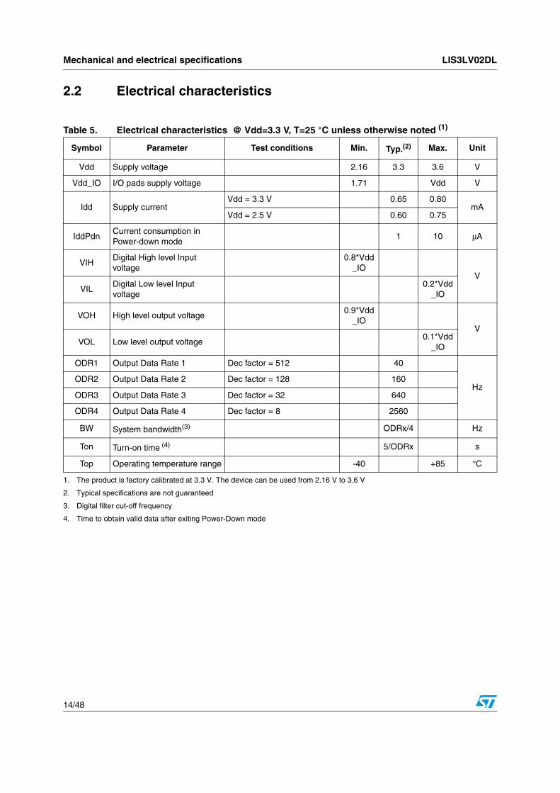
7.26 DD_SRC (39h)
Direction detector source register.
XHIE
Enable interrupt generation on X High event. Default value: 0
(0: disable interrupt request;
1: enable interrupt request on measured accel. value higher than preset threshold)
XLIE
Enable interrupt generation on X Low event. Default value: 0
(0: disable interrupt request;1: enable interrupt request on measured accel. value lower than preset threshold)
Table 61. Register description (continued) (38h)
Table 62. Register (39h)
X IA ZH ZL YH YL XH XL
Table 63. Register description (39h)
IA
Interrupt event from direction change.
(0: no direction changes detected;
1: direction has changed from previous measurement)
ZH
Z High. Default value: 0
(0: Z below THSI threshold; 1: Z accel. exceeding THSE threshold along positive direction of acceleration axis)
ZLZ Low. Default value: 0(0: Z below THSI threshold;
1: Z accel. exceeding THSE threshold along negative direction of acceleration axis)
YH
Y High. Default value: 0
(0: Y below THSI threshold;
1: Y accel. exceeding THSE threshold along positive direction of acceleration axis)
YL
Y Low. Default value: 0
(0: Y below THSI threshold; 1: Y accel. exceeding THSE threshold along negative direction of acceleration axis)
XHX High. Default value: 0(0: X below THSI threshold;
1: X accel. exceeding THSE threshold along positive direction of acceleration axis)
XL
X Low. Default value: 0
(0: X below THSI threshold;
1: X accel. exceeding THSE threshold along negative direction of acceleration axis)

LIS3LV02DL Register description
41/48
7.27 DD_ACK (3Ah)Dummy register. If LIR bit in DD_CFG register is set to ‘1’, a reading at this address allows the DD_SRC register refresh. Read data is not significant.
7.28 DD_THSI_L (3Ch)
7.29 DD_THSI_H (3Dh)
7.30 DD_THSE_L (3Eh)
7.31 DD_THSE_H (3Fh)
Table 64. Register (3Ch)
THSI7 THSI6 THSI5 THSI4 THSI3 THSI2 THSI1 THSI0
Table 65. Register description (3Ch)
THSI7, THSI0 Direction detection Internal Threshold LSB
Table 66. Register (3Dh)
THSI15 THSI14 THSI13 THSI12 THSI11 THSI10 THSI9 THSI8
Table 67. Register description (3Dh)
THSI15, THSI8 Direction detection Internal Threshold MSB
Table 68. Register (3Eh)
THSE7 THSE6 THSE5 THSE4 THSE3 THSE2 THSE1 THSE0
Table 69. Register description (3Eh)
THSE7, THSE0 Direction detection External Threshold LSB
Table 70. Register (3Fh)
THSE15 THSE14 THSE13 THSE12 THSE11 THSE10 THSE9 THSE8
Table 71. Register description (3Fh)
THSE15, THSE8 Direction detection External Threshold MSB

Typical performance characteristics LIS3LV02DL
42/48
8 Typical performance characteristics
8.1 Mechanical characteristics at 25°C
Figure 12. X-axis zero-g level at 3.3 V Figure 13. X-axis sensitivity at 3.3 V
Figure 14. Y-axis zero-g level at 3.3 V Figure 15. Y-axis sensitivity at 3.3 V
−60 −40 −20 0 20 40 600
2
4
6
8
10
12
14
16
18
20
Zero−g Level Offset [mg]
Per
cent
of p
arts
[%]
940 960 980 1000 1020 1040 1060 1080 1100 11200
5
10
15
20
25
Sensitivity [LSB/g]
Per
cent
of p
arts
[%]
−60 −40 −20 0 20 40 600
5
10
15
20
25
Zero−g Level Offset [mg]
Per
cent
of p
arts
[%]
940 960 980 1000 1020 1040 1060 1080 1100 11200
5
10
15
20
25
Sensitivity [LSB/g]
Per
cent
of p
arts
[%]

LIS3LV02DL Typical performance characteristics
43/48
8.2 Mechanical characteristics derived from measurement in the -40°C to +85°C temperature range
Figure 16. Z-axis zero-g level at 3.3 V Figure 17. Z-axis Sensitivity at 3.3 V
−60 −40 −20 0 20 40 600
5
10
15
20
25
Zero−g Level Offset [mg]
Per
cent
of p
arts
[%]
940 960 980 1000 1020 1040 1060 1080 1100 11200
5
10
15
20
25
30
Sensitivity [LSB/g]
Per
cent
of p
arts
[%]
Figure 18. X-axis zero-g level change vs. temperature at 3.3 V
Figure 19. X-axis sensitivity change vs. temperature at 3.3 V
−1.5 −1 −0.5 0 0.5 1 1.50
2
4
6
8
10
12
14
16
18
20
Zero−g Level drift [mg/oC]
Per
cent
of p
arts
[%]
−0.05 −0.045 −0.04 −0.035 −0.03 −0.025 −0.02 −0.015 −0.01 −0.005 00
5
10
15
20
25
Sensitivity drift [%/oC]
Per
cent
of p
arts
[%]

Typical performance characteristics LIS3LV02DL
44/48
8.3 Electro-mechanical characteristics at 25°C
Figure 20. Y-axis zero-g level change vs. temperature at 3.3 V
Figure 21. Y-axis sensitivity change vs. temperature at 3.3 V
Figure 22. Z-axis zero-g level change vs. temperature at 3.3 V
Figure 23. Z-axis sensitivity change vs. temperature at 3.3 V
−1 −0.8 −0.6 −0.4 −0.2 0 0.2 0.4 0.6 0.8 10
5
10
15
20
25
30
35
40
Zero−g Level drift [mg/oC]
Per
cent
of p
arts
[%]
−0.015 −0.01 −0.005 0 0.005 0.01 0.015 0.020
5
10
15
20
25
Sensitivity drift [%/oC]
Per
cent
of p
arts
[%]
−2.5 −2 −1.5 −1 −0.5 0 0.5 1 1.5 2 2.50
5
10
15
20
25
Zero−g Level drift [mg/oC]
Per
cent
of p
arts
[%]
−0.05 −0.04 −0.03 −0.02 −0.01 0 0.01 0.020
5
10
15
20
25
30
Sensitivity drift [%/oC]
Per
cent
of p
arts
[%]
Figure 24. X and Y axis zero-g level as function of supply voltage
Figure 25. Z axis zero-g level as function of supply voltage
2 2.2 2.4 2.6 2.8 3 3.2 3.4 3.6−60
−40
−20
0
20
40
60
Supply Voltage [V]
Zer
o−g
leve
l [m
g]
2 2.2 2.4 2.6 2.8 3 3.2 3.4 3.6−40
−20
0
20
40
60
80
100
Supply Voltage [V]
Zer
o−g
leve
l [m
g]

LIS3LV02DL Typical performance characteristics
45/48
Figure 26. Current consumption in Power-Down mode (Vdd=3.3 V)
Figure 27. Current consumption in operational mode (Vdd=3.3 V)
−5 −2.5 0 2.5 50
5
10
15
20
25
30
35
Current consumption [uA]
Per
cent
of p
arts
[%]
550 600 650 700 7500
2
4
6
8
10
12
14
16
Current consumption [uA]
Per
cent
of p
arts
[%]

Package information LIS3LV02DL
46/48
9 Package information
In order to meet environmental requirements, ST offers these devices in ECOPACK® packages. These packages have a lead-free second level interconnect. The category of second Level Interconnect is marked on the package and on the inner box label, in compliance with JEDEC Standard JESD97. The maximum ratings related to soldering conditions are also marked on the inner box label. ECOPACK® is an ST trademark.
ECOPACK® specifications are available at: www.st.com.
Figure 28. LGA-16 mechanical data and package dimensions
OUTLINE ANDMECHANICAL DATA
DIM.mm inch
MIN. TYP. MAX. MIN. TYP. MAX.
A1 0.92 1 0.0394
A2 0.7 0.0276
A3 0.180 0.220 0.260 0.0071 0.0087 0.0102
D1 4.250 4.400 4.550 0.1673 0.1732 0.1791
E1 7.350 7.500 7.650 0.2894 0.2953 0.3012
e 1.0 0.0394
d 0.3 0.0118
L1 5.000 0.1969
N 2.5 0.0984
N1 1.2 0.0472
P1 0.965 0.975 0.985 0.0380 0.0384 0.0388
P2 0.64 0.65 0.66 0.0252 0.0256 0.0260
T1 0.75 0.8 0.85 0.0295 0.0315 0.0335
T2 0.45 0.5 0.55 0.0177 0.0197 0.0217
R 1.200 1.600 0.0472 0.0630
h 0.150 0.0059
k 0.050 0.0020
i 0.100 0.0039
s 0.100 0.0039
LGA16 (4.4x7.5x1mm)Land Grid Array Package
7863679 B
E1
P2L1
T2
D1
P1
BACi
A3
R
A2
A1
1 2 4 5 6
7
8
16
15
91011121314
3N1
e
T1
s
eN
d
Detail A
Detail A
Metal Pad
seating plane
Solder maskopening
i
E
C
DD
A
EB
i
BACh
Dk
BAChBACi
Ek
k(4 x)

LIS3LV02DL Revision history
47/48
10 Revision history
Table 72. Document revision history
Date Revision Changes
15-Feb-2006 1 Initial release.
15-Jan-2008 2
Added two new sections:
Section 2.3: Communication interface characteristics and Section 8: Typical performance characteristics.
Content reworked to improve readability

LIS3LV02DL
48/48
Please Read Carefully:
Information in this document is provided solely in connection with ST products. STMicroelectronics NV and its subsidiaries (“ST”) reserve theright to make changes, corrections, modifications or improvements, to this document, and the products and services described herein at anytime, without notice.
All ST products are sold pursuant to ST’s terms and conditions of sale.
Purchasers are solely responsible for the choice, selection and use of the ST products and services described herein, and ST assumes noliability whatsoever relating to the choice, selection or use of the ST products and services described herein.
No license, express or implied, by estoppel or otherwise, to any intellectual property rights is granted under this document. If any part of thisdocument refers to any third party products or services it shall not be deemed a license grant by ST for the use of such third party productsor services, or any intellectual property contained therein or considered as a warranty covering the use in any manner whatsoever of suchthird party products or services or any intellectual property contained therein.
UNLESS OTHERWISE SET FORTH IN ST’S TERMS AND CONDITIONS OF SALE ST DISCLAIMS ANY EXPRESS OR IMPLIEDWARRANTY WITH RESPECT TO THE USE AND/OR SALE OF ST PRODUCTS INCLUDING WITHOUT LIMITATION IMPLIEDWARRANTIES OF MERCHANTABILITY, FITNESS FOR A PARTICULAR PURPOSE (AND THEIR EQUIVALENTS UNDER THE LAWSOF ANY JURISDICTION), OR INFRINGEMENT OF ANY PATENT, COPYRIGHT OR OTHER INTELLECTUAL PROPERTY RIGHT.
UNLESS EXPRESSLY APPROVED IN WRITING BY AN AUTHORIZED ST REPRESENTATIVE, ST PRODUCTS ARE NOTRECOMMENDED, AUTHORIZED OR WARRANTED FOR USE IN MILITARY, AIR CRAFT, SPACE, LIFE SAVING, OR LIFE SUSTAININGAPPLICATIONS, NOR IN PRODUCTS OR SYSTEMS WHERE FAILURE OR MALFUNCTION MAY RESULT IN PERSONAL INJURY,DEATH, OR SEVERE PROPERTY OR ENVIRONMENTAL DAMAGE. ST PRODUCTS WHICH ARE NOT SPECIFIED AS "AUTOMOTIVEGRADE" MAY ONLY BE USED IN AUTOMOTIVE APPLICATIONS AT USER’S OWN RISK.
Resale of ST products with provisions different from the statements and/or technical features set forth in this document shall immediately voidany warranty granted by ST for the ST product or service described herein and shall not create or extend in any manner whatsoever, anyliability of ST.
ST and the ST logo are trademarks or registered trademarks of ST in various countries.
Information in this document supersedes and replaces all information previously supplied.
The ST logo is a registered trademark of STMicroelectronics. All other names are the property of their respective owners.
© 2008 STMicroelectronics - All rights reserved
STMicroelectronics group of companies
Australia - Belgium - Brazil - Canada - China - Czech Republic - Finland - France - Germany - Hong Kong - India - Israel - Italy - Japan - Malaysia - Malta - Morocco - Singapore - Spain - Sweden - Switzerland - United Kingdom - United States of America
www.st.com