Embed Size (px)
Citation preview

Micromachining technology - [email protected]
Péter FürjesE-mail: [email protected]
MICROMACHINING TECHNOLOGY

Micromachining technology - [email protected]
MEMS: Micro-ElectroMechanical Systems
Miniaturised devices and systems: in the range between 100nm and 1000µm
Batch processes
Low costs
High sensitivity Low power
consumption Integrability
SolidState Technology, Ramesh Ramadoss, MEMS devices for biomedical applicationshttp://electroiq.com/blog/2013/10/mems-devices-for-biomedical-applications/
Fabrication technology: SILICON micromachining Photolithography Physical and chemical layer deposition (metals, dielectrics) Wet and dry etching
MEMS / BIOMEMS - DEFINITION

Micromachining technology - [email protected]
MEMS: „2D” IC technology 3D structures membranes, suspended structures, movable elements, microfluidic applications: channels, chambers, reactors etc.
Microfabrications: processes and devices: different from traditional mechanical fabrication technologiesmainly „dry” and „wet” chemical etching and electrochemical methods,
BUT classic processes (laser or diamond blade cutting)
Typical dimensions: 1-500 mmThickness of the Si crystal: 380-500-1000 mm
MICROMECHANICS

Micromachining technology - [email protected]
3rd solution: Thin single crystalline layers: ”Smart Cut” / SOI (silicon-on-insulator)
Bulk SurfaceDimensions 2-3 m < a < 100-500 m a < 2-3 mThermal isolation + -Mechanical stability + -Membranes Single crystalline amorphous or polycrystalline
BULK vs. SURFACE MICROMACHINING

Micromachining technology - [email protected]
Typical problem: sticking
Solution: inbuilt keeperor perforated structuresor dry etchingor supercritical drying
BULK vs. SURFACE MICROMACHINING

Micromachining technology - [email protected]: SURFACE MICROMACHINING

Micromachining technology - [email protected]: BULK MICROMACHINING

Micromachining technology - [email protected]
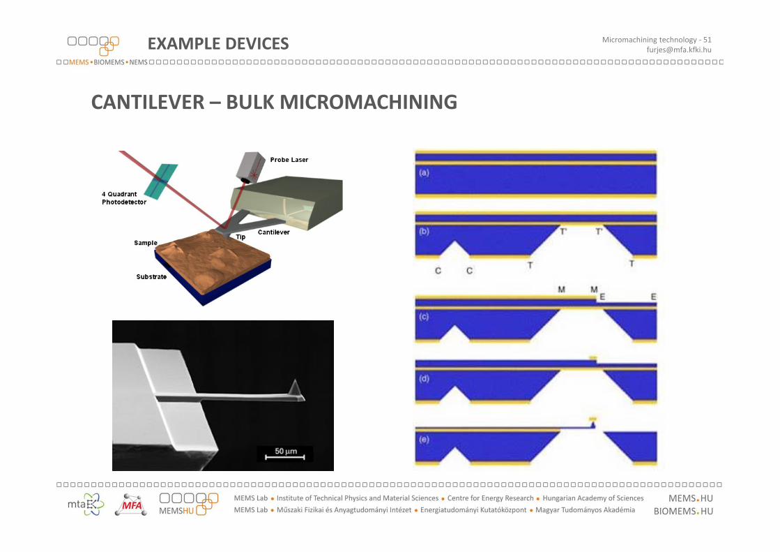
1. Surface treatments: cleaning, dehydratation
2. Photoresist spincoat / prebake
3. Exposure / development
Postexposurebake / softbakehardbake
4. Processing withphotoresist masking
5. Photoresist removal, stripping, cleaning
PHOTOLITHOGRAPHY PROCESS
SUBSTRACTIVE PHOTOLITHOGRAPHY
Micromachining technology - [email protected]
1. Surface treatments: cleaning, dehydratation
2. Photoresist spincoat / prebake
3. Exposure / development
Postexposurebake / softbake
4. Layer deposition
5. Photoresist removal, stripping, cleaning
PHOTOLITHOGRAPHY PROCESS – LIFT-OFF
ADDITIVE PHOTOLITHOGRAPHY

Micromachining technology - [email protected]
Spincoater – hotplate mask alligner developer
Hg lamp: 436 nm (g-line), 405 nm (h-line), 365 nm (i-line)
KrF laser: 248 nm / ArF lézer: 193 nm
Next generation: extreme UV (EUV): 13.5 nm
PHOTOLITHOGRAPHY PROCESS
EQUIPMENTS - RADIATION

Micromachining technology - [email protected]
APPLICATIONS Microelectronics, semiconductor processing Micro-electromechanical systems (sensors, actuators, MEMS) Thermal conducting coatings (BeO, AlN, diamond) Photovoltaic devices (solar cells)
amorphous and microcrystalline Si layers on glass and polimer substrates compound-semiconductors (CuInGaSe, CdTe) single- and multicrystalline Si solar cells (HIT)
Optical applications (filters, gratings, antireflexion layers, mirrors, etc.) Abrasion-resistant coatings
protection of optical devices (deposited diamond layers) hard coating of tools (TiN, WC, B4C, diamond, DLC) coatings of human prosthesis
Corrosion-resistant coatings Decoration coatings
THIN FILMS

Micromachining technology - [email protected]
STANDARD REQUIREMENTS
homogeneous thickness on the substrate homogeneous composition homogeneous structure (amorphous, polycrystalline, epitaxal) homogeneous physical and chemical properties compactness (sponge vs. layer, pinholes) adequate adhesion low thermomechanical stress special requirements
(friction, wettability, biocompatibility, etc..)
economical deposition rate infrastructural maintenance
step coverage
THIN FILMS

Micromachining technology - [email protected]
TECHNOLOGIES
Physical methods (PVD, Physical Vapour Deposition)Solid source: vacuum evaporation
sputtering: DC, RF, magnetronMBE (Molecular Beam Epitaxy)
Melt source: LPE (Liquid Phase Epitaxy)(single crystal growing, Czohralsky, Floating zone)
Chemical methodsElectrolite source: plating(solution, suspension) setting, sol-gel technics)gázfázisból: CVD (Chemical Vapour Deposition)
VPE (Vapour Phase Epitaxy)MOCVD (Metal Organic ….)LPCVD (Low pressure…)PECVD (Plasma enhanced…) MWCVD (MicroWave…)PACVD (Photon assisted…, or plasma assisted)ALCVD (Atomic Layer.. ALD(ep..), ALEpitaxy)
THIN FILMS

Micromachining technology - [email protected]
CVD – CHEMICAL VAPOUR DEPOSITION
Chemical reaction of one or more gas phase reagents (precursors) on a solid substrate Surface catalysed reaction (not in the gas space) Solid product
THIN FILMS

Micromachining technology - [email protected]
Atmospheric CVD - APCVD
Small free path Reaction rate control: transport (reagent or product) Thermal activation
egyenletesség ±10%, főleg egyszeletes reaktorok
x= xvo)1/2
kinematicviscosity
densityThickness homogeneity ±10%, single wafer reactors
SiO2: silane + oxygen / 450oC
CHEMICAL VAPOUR DEPOSITIONS

Micromachining technology - [email protected]
LOW PRESSURE CVD - LPCVD
Long free path Reaction rate control: chemical reaction Thermal / plasma activation
Thickness homogeneity ±2-6%, batch and single wafer reactors
CHEMICAL VAPOUR DEPOSITIONS

Micromachining technology - [email protected]
ALD – ATOMIC LAYER DEPOSITION
Reaction rate control: chemisorption Thermal / plasma activation
atomic / molecular precision excellent homogeneity excellent step coverage batch and single wafer reactors
Typical materials: Al2O3, ZnO, HfO, …
CHEMICAL VAPOUR DEPOSITIONS

Micromachining technology - [email protected]
CHEMICAL ETCHING
Etching: removal of the solid material of the substrate by chemical reaction
Reagent: liquid or gas (or vapour, or plasma)
Wet etching: Chemical reaction on the liquid / solid interface – causing dissolution of solid
material
Dry etching: Gas or vapour phase reagents at high temperature Gas phase reagent at low temperature and pressure, active particles with extreme
high reactivity, generated by RF induced plasma discharge (free radicals or excitedneutral particles) – isotropic etching
Physical etching – non or moderate selective sputtering of the substrate atoms and molecules – directional / anisotropic etching
ETCHING

Micromachining technology - [email protected]
APPLICATIONS in IC TECHNOLOGY
Semiconductor wafer processing Elimination of mechanical defects by chemical polishing High quality surface development by chemical-mechanaical polishing
CMOS technology / micromachining Photoresist development Selective or total removal of oxides or nitrides Patterning of metal layers Selective or total removal of organic layers Contour etching: engineered undetcut profiles Anisotropic etching of si in MEMS structures Etching of polycristalline Si in MOS structures (poly-gate)
Analitical applications:e.g. exploring foults (pinholes, crystalline foults
Packaging semiconductor devices: e.g. refreshing metal surfaces
ETCHING

Micromachining technology - [email protected]
WET CHEMICAL ETCHING
Requirements against the etching processes:
uniform etch rate on the whole substrate surface
high selectivity for the masking layer(for photoresist or other layer)
high selectivity for substrate material(vlayer / vsubstrate >10..100)
adequate etch rate corresponding to the thickness of the layer to be etched ( 0,1-1 m/min)
possibly controlled by chemical reaction(not by transport)
WET ETCHING

Micromachining technology - [email protected]
WET ETCHING TECHNIQUES
Immersion etching High wafer number / economicalsti Rate control: temperature / stirring (bubbleing / stirring / ultrasonic tub)
Spray etching Effective etch rate control (parameters: vaporisation drop size / pressure) Enhanced etch rate due to the continously fresh etchant Single wafer
Chemo-mechanical etching Wafer polishing (Si or polymers)
Electrochemical etching Selectivity and etch rate control
(parameters: potential or current)
WET ETCHING

Micromachining technology - [email protected]
DIRECTION DEPENDENCY OF WET ETCHING
Isotropic etching: direction independent etch rate Etching of amorphous and polycrystalline materials is typically isotropic Typically diffusion limited processes
Anisotropic etching: direction dependent etch rate Etching of crystalline materials could be isotropic and anisotropic
according to the composition of the etching solution and the reaction kinetics Typically reaction limited processes
WET ETCHING

Micromachining technology - [email protected]
ETCHING OF SILICON
Isotropic:uniform etch rate in each crystallic directions(e.g. poly-Si etchant - HF-HNO3-CH3COOOH )
Anisotropic:etch rates are altering according to thedifferent crystallic directions(e.g. alkaline etchants – KOH)
WET ETCHING

Micromachining technology - [email protected]
Crystalline structure of silicon: face centered cubic
Si-Si bonding energies: E(SiSi)(111) >> E(SiSi)(100) > E(SiSi)(110)
Etching rates: v<111> << v<100> < v<331>
DIRECTION DEPENDENT ETCHING OF SI
Typical crystalline planes:
WET ETCHING

Micromachining technology - [email protected] ETCHING

Micromachining technology - [email protected]
PLASMA ETCHING
Plasma Glow
Low gas pressure (1 mtorr-1 torr) High electric field on the electrodes,
13.56 MHz RF Ionisation of the gas atoms:
e- + ions
plasma glow – conducting gas(ions, free radicals, electrons, natural particles),Particles are excited by the quick electronsand emit photons after relaxation.
DRY ETCHING

Micromachining technology - [email protected]
DRY ETCHING PROCESSES
Effective chemical etching by reactive radicals (atomic F) Directional / anisotropic physical etching by charged particles
DRY ETCHING

Micromachining technology - [email protected]
DRY CHEMICAL ETCHING
Free radicals (neutral, having non-bonding electronpair) – extremely reactive
CF4 + e- → CF3 + F + e-
4F + Si → SiF4
Volatile products – must get away from the surfacefor continuous etching
Additive gases: possibly support the generation of reactive free radicals, enhancing etch rates!
e.g. O2 gas reacts with dissociated CF3, CF2 molecules, preventing the recombination to CF4, enhancing the concentrtion of free F radicalsBUT: O2 dillutes the etchant gas!
Isotropic etching:1. Isotropic angular distribution
of the incident velocityvector (particles)
2. Low surface adhesion / sticking coefficient(long path till reaction
HIGH SELECTIVITY
DRY ETCHING

Micromachining technology - [email protected]
DRY PHYSICAL ETCHING
Positive ions are accelerating towards the electrodesdue to Vp (one is the substrate holder)
Anisotropic etching:– Direction dependent etching rate of the incident
ions due to the directional electric field– High adhesion / sticking coefficient – reaction at the
moment of incidence LOW SELECTIVITY
Technologies: Sputtering or ion etching Focused Ion Beam etching (FIB) Magnetically localised ion etching
DRY ETCHING

Micromachining technology - [email protected]
ION-ASSISTED ETCHING
Chemical-physical dry etching(combination of the two processes)Ions + natural free radicals etch dependently:
Can increase selectivity and orientation dependentreaction rate
The etch rate is not the sum (higher) The etch profile is not a linear combinatin, but similar
to physical etching (vertical etch rate increases)
The ion bombardment enhances one of the component of thechemical etching (surface adsorption, etching reaction, generation / removal of the product) anisotropic way
Technics: Reactive ion etching, sputtering Reactive ion beam etching Chemical enhanced ionbeam etching
DRY ETCHING

Micromachining technology - [email protected]
PLASMA ETCHING EQUIPMENTS I.
Cylindrical / barrel type plasma etcher Wafer in holder (not on the electrode), multiwafer process Isotropic chemical etching, high selectivity, low fault generation Inhomogeneous etch rate on the wafer p=10-1000mtor
For not criticaletching stepsresist removalin O2 (ashing)
DRY ETCHING

Micromachining technology - [email protected]
Planar type plasma etcher - Plasma mode The wafer is on the (bigger) grounded electrode facing to the oposite electrode
– higher homogeneity, mainly chemical, adequate selectivity, slight anisotropy Weak ion bombardment , potential difference 10-100V The smaller electrode is sputtered p=10-500mtorr Ion concentration ~ 109-1010cm-3
PLASMA ETCHING EQUIPMENTS II.
For not critical etching stepsresist removal in O2 (ashing)Isotropic silicon-nitride etching
DRY ETCHING

Micromachining technology - [email protected]
Planar type plasma etcher – RIE (Reactive Ion Etching) mode The wafer is on the smaller electrode – single wafer process The bigger electrode is grounded and connected to the chamber wall,
higher potential difference in the range of 100-800V (bias) - ion enhanced / assisted anisotropic etching
More directional etch in case of low pressure, but lower plasma density(10-100 mtorr), ion concentration ~ 109-1010 cm-3
Moderate etching rate 100 nm/min Lattice faults, charging, trenching
PLASMA ETCHING EQUIPMENTS III.
Examples:SiO2: CHF3poly-Si, Si3N4: SF6+ O2, NF3Al: Cl2, BCl3
DRY ETCHING

Micromachining technology - [email protected]
Independent plasma density and ion energy
ECR (electron-cyclotron-resonance) or ICP (inductivelycoupled plasma) source generates 1011-1012 ion/cm3
plasma density, without high sheath bias – lower pressurecan be applied 1-10 mTorr – highly directional (less collisionin the sheath)
RF source developes the potential difference, defines thebombarding ion energy, (can be decreased besides high ion density – decreased substrate deterioration
high etch rate: some m/min
Similar effect as in case of ion enhanced etching!
PLASMA ETCHING EQUIPMENTS IV. HDPE - High Density Plasma Etching
DRY ETCHING

Micromachining technology - [email protected]
DRIE INTRODRIE – Deep Reactive Ion EtchingEtching depth / trench width > 10:1 (MEMS, DRAM capacitors)Doubled power sources: ICP to achieve extremely high density reactive radicals + ions CCP DC self-bias for definition ion energies
Si DRIEGas composition: halogen based accelerated plasma etching F-based, (e.g. SF6 ) quick isotropic etching Cl-, Br-based (e.g. Cl2, HBr) anisotropic with ion assisted
etching, but slower and poisoning
Mixed mode DRIE / Cryo
SF6 + O2 @ cryo °C
Pulsed mode DRIE / Bosch
SF6 + C4F8 @ RT
DRY ETCHING

Micromachining technology - [email protected]
• PassivationC4F8 n CF2 (PTFE)
• EtchingSF6 F + ionsion bombardment + polymer etching(excluding the vertical walls)
• SF6 isotropic orslightly anisotropic Si etching
DRIE – BOSCH PROCESS
DRY ETCHING

Micromachining technology - [email protected] ETCHING

Micromachining technology - [email protected]
ANODIC BONDING
• Si + Special glass (high alcaline-ion concentration)• Moving Na+ ions – depleted space-charge layer• Covalent bonding of silicon and oxygen
• Low sensitivity for surface roughness
WAFER BINDING

Micromachining technology - [email protected]
LIGA (KIT)
Lithographie, Galvanoformung, Abformung (Lithography, Electroplating, Casting) Fabrication microstructures with high aspect ratio (100:1) Vertical sidewalls, 10nm surface roughness (optical structures) Height: from 10m to some mm X-ray LIGA (PMMA) / UV LIGA (SU-8)
LIGA

Micromachining technology - [email protected]
FABRICATION PDMS POLYMER MICROFLUIDIC STRUCTURES
Silicon substrate
SU-8 photoresist
UV exposure
Advantages: biocompatibility, flexibility, transparency cheap, fast, easy to use covalent bonding to Si, glass and PDMS surfaces
channels
mask
SOFT LITHOGRAPHY
Disdvantages: hydrophobic non-specific molecule (e.g. protein)
adsorption

Micromachining technology - [email protected]
Multi-layered 3D SU-8 technology for structuring moulding master FAST PROTOTYPING – PDMS moulding / casting
Herin
g-bo
nety
pech
aotic
mixe
r
SOFT LITHOGRAPHY
FABRICATION PDMS POLYMER MICROFLUIDIC STRUCTURES

Micromachining technology - [email protected]
MICROPHONEHigh Performance MEMS microphones (3-4 pcs / phone)
Top electrode: Au SiO2 / SiNx membraneBottom-electrode: n-Si
dACo 2d
AdC
DRIE (deepreactive ion-etching) etchedmembrane
EXAMPLE DEVICES

Micromachining technology - [email protected]
MICROPHONE – BULK MICROMACHINING (KOH)
EXAMPLE DEVICES

Micromachining technology - [email protected]
MICROPHONE – BULK / SURFACE MICROMACHINING (COMBO)
EXAMPLE DEVICES

Micromachining technology - [email protected]
High throughput channel arrayin a single substrate
Utilysing the whole cross-section of the shaft
Orientation independentpositioning
CMOS compatible fabricationtechnology
High quality surface applicablefor further lithographic steps
DRUG DELIVERY CHANNELSIN SILICON NEURAL PROBE
EXAMPLE DEVICES
Micromachining technology - [email protected]
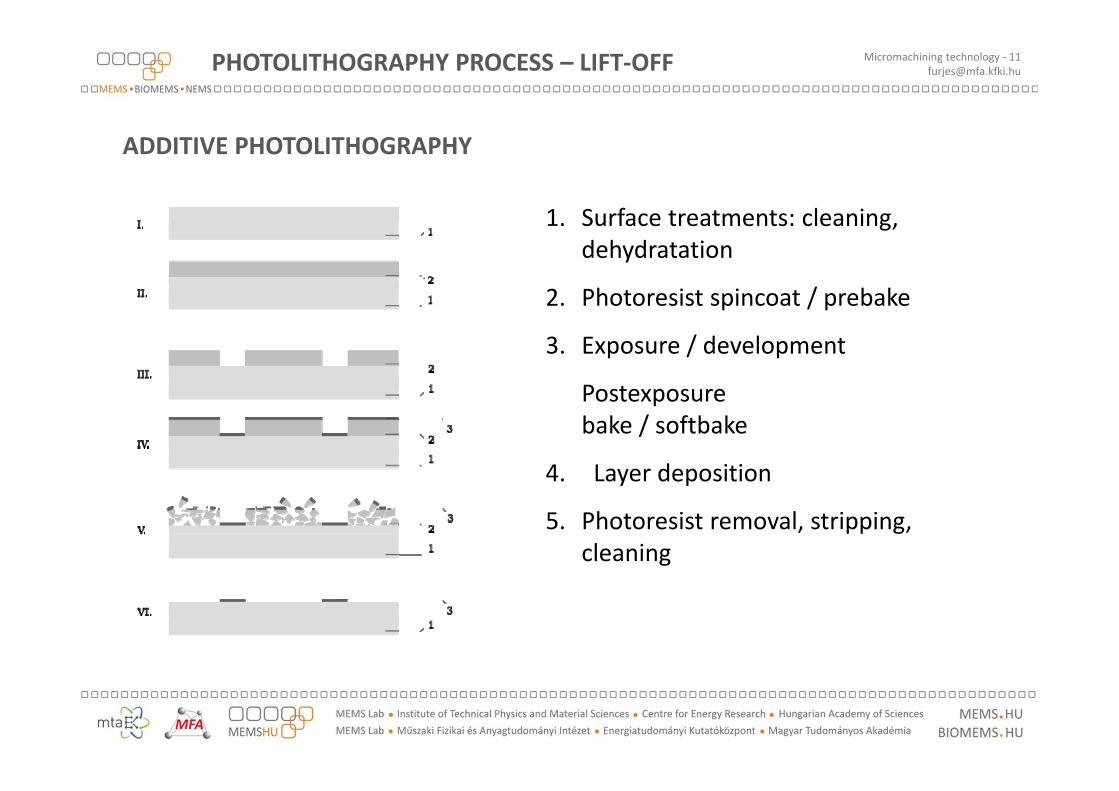
5µm
FABRICATION TECHNOLOGY OF BURRIED CHANNELS
EXAMPLE DEVICES

Micromachining technology - [email protected]
ARTIFICIAL TACTILE RECEPTORS
BIOMIMETIC FORCE DETECTIONANALOGY of TACTILE SENSING static pressure, low and high frequency
vibration, SHEAR FORCES!!! lubricity, roughness, patterns, shape…
Human tactile receptors
IN VIVO CONTACT FORCE MEASUREMENT
visualization of contact forcebetween catheter tip and the heart wall during catheter ablation
Tactile (force) feedback duringMIS surgery
SENSOR INTEGRATION

Micromachining technology - [email protected]
ARTIFICIAL TACTILE RECEPTORS
MEMS BASED 3D VECTORIAL FORCE SENSOR 3D MEMS technology based realisation of
crystalline Silicon sensing elements piezoresistive read-out principle
ACTUAL FEATURES sensitivity and resolution: similar to human fingers max. density: 8x8 taxels with CMOS addressing read-out circuitry neuromorph flexible polymer covering
8x8 (7x7mm)40 contacts, MEMS + CMOS
PDMS rubber hemispheresas 1st level packaging
SENSOR INTEGRATION
Micromachining technology - [email protected]
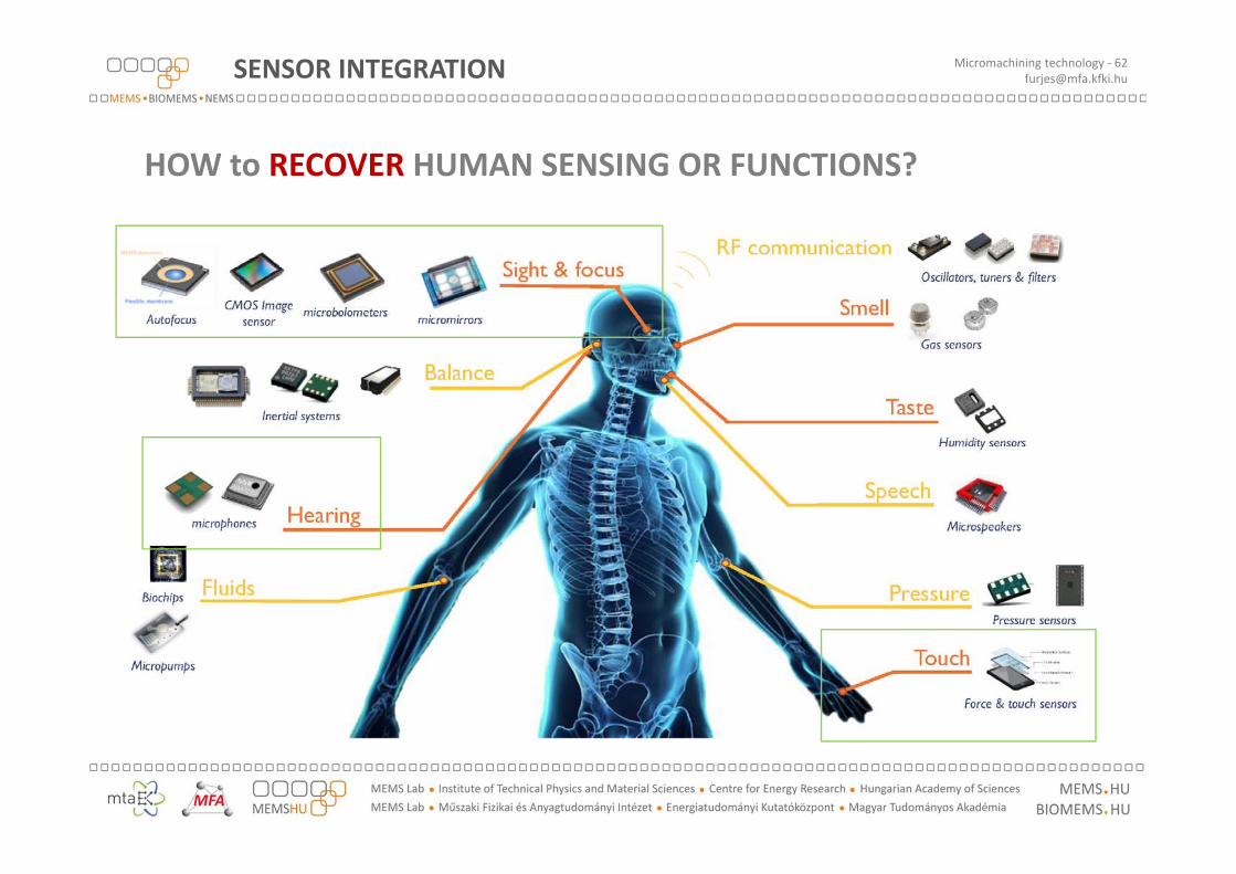
HOW to RECOVER HUMAN SENSING OR FUNCTIONS?
SENSOR INTEGRATION

Micromachining technology - [email protected]
IMPLANTABLE MICROSYSTEMSHEARING:COCLEAR IMPLANTNEURAL CELL ACTIVITY RECORDING
IMAGING INTERFACING / STIMULATION
SENSOR INTEGRATION

Micromachining technology - [email protected]
FUTURE TRENDS IN MEDICAL MEMS APPLICATIONS
BRAIN-MACHINE INTERFACING
IMPLANTABLE AUTONOMOUS DEVICES Energy harvesting SENSING: continous
health monitoring ACTUATION:
immediate treating(drug injection)
INTERNET of THINGS
SMART SYSTEMS – HIGH DENSITY INTEGRATION Energy supply Sensing Signal / Data processing Communication Actuation
NANOTECHNOLOGY diagnostics & treating
PERSONALMEDICINE
Philips
University of Illinois
SENSOR INTEGRATION

Micromachining technology - [email protected]
Nanoprocessing and analysis / characterisation:E-BEAM, FIB, SEM, TEM, AFM, XPS, EDX, Auger, SIMS
Zeiss-SMT LEO 1540 XB SEM,Canion FIB nanoprocessing system
SEM and focused ion beam (FIB),Gas injection system (GIS) (EBAD, IBAD)and Energy Dispersive Spectroscopy (EDS)
MEMS laboratory:300+150 m2 clean room (4inch wafers) - 1mm resolution - mask shop(Heidelberg laser PG & direct writing),
Mask alligner / nanoimprinting system (Karl Süss MA 6, Quintel), DRIE (Oxford Instruments Plasmalab 100),Physical and chemical layer deposition techniques
(vacuum evaporation, sputtering, 2x4 diffusion tubes, LPCVD, ALD),Wafer bonder (Karl Süss BA 6), ion implanter, etc.
MEMS LAB AT MTA EK MFA

Micromachining technology - [email protected]
Nanoprocessing and analysis / characterisation:RAITH 150 E-BEAM
Direct writing / mask processing - Ultra high resolution
Thermal field emission (Schottky) source. GEMINI (state-of-the-art low kV
performance, beam energy: 200 V – 30 kV.
6'' laser interferometer stage electrostatic clamping automatic sample levelling by 3-points piezo motor
Writable surface: 0.5 – 800 m Fixed Beam Moving Stage (FBMS) Fast Pattern Generator max. 10 MHz writing frequency Minimum dwell time: 2 ns.
Measurement functions: linewidth and long-range laser interferometry based 2 nm resolution Magnifications: 20 – 900.000 X.
MEMS LAB AT MTA EK MFA

Micromachining technology - [email protected]
SPECIAL THANKS TO
R. E. GyurcsányiBudapest University of Technology and Economics
T. Mészáros, P. SoósSemmelweis University, Hungary
M. Varga, B. SzabóElektronika 77 Ltd., Hungary
J. Prechl, K. PapEötvös Loránd University, Immunology Dept.
BioMEMS Group:
Supported by
via P3SENS / CAJAL4EU / INCITE / PAMIAQ / VKSZ_14 projects
www.biomems.hu
ACKNOWLEDGEMENT