Embed Size (px)
Citation preview
Mems Oscillator, High Performance Differential Oscillator, LVPECL and LVDS 1.000 MHz to 220.000MHz IM840 Series
ILSI America Phone 775-851-8880 Fax 775-851-8882 email: [email protected] www.ilsiamerica.com
Specifications subject to change without notice
Rev 05/17/17_B
Page 1 of 7
Features: MEMS Technology Direct pin to pin drop-in replacement for industry-standard packages 0.6 pSec RMS phase jitter (random) over 12 kHz to 20 MHz bandwidth LVPECL and LVDS output signaling types Industry-standard package 3.2 x 2.5, and 5.0 x 3.2 mm x mm Pb-free, RoHS and REACH compliant
Typical Applications: Fibre Channel Server and Storage GPON, EPON 100M / 1G /10G Ethernet
Electronic Specifications: Frequency Range 1.000 MHz to 220.000 MHz
Frequency Stability See Part Number Guide Inclusive of all changes in Operating Temp. Range, Load, and Voltage.
First Year Aging ±2.0 ppm max +25°C ±2.0°C
10 Years Aging ±5.0 ppm max +25°C ±2.0°C
Operating Temperature See Part Number Guide
Supply Voltage (Vdd) ±10% See Part Number Guide
Input Voltage High 70% of Vdd min Pin 1, OE or ST
Input Voltage Low 30% of Vdd max Pin 1, OE or ST
Input Pull-up Impedance 100 kΩ typ., 250 kΩ max 2.0 MΩ min
Pin 1, OE logic high or logic low, or ST logic high Pin 1, ST logic low
Start-up Time 6.0 mSec typ., 10.0 mSec max Measured from the time Vdd reaches its rated minimum values
Resume Time 6.0 mSec typ., 10.0 mSec max Measured from the time ST pin crosses 50% threshold.
Symmetry 45%/55%
LVPECL, DC and AC Characteristics
Current Consumption 61 mA typ., 69 mA max Excluding Load Termination Current, Vdd = +3.3 V or +2.5 V
OE Disable Supply Currrent 35 mA max OE = Low
Output Disable Leakage Current 1 µA max OE = Low
Standby Current 100 µA max ST = Low, for all Vdds
Maximum Output Current 30 mA max Max average current drawn from OUT+ or OUT-
Logic “1” Vdd -1.1 min / Vdd – 0.7 max See figure 1(a)
Logic “0” Vdd -1.9 min / Vdd – 1.5 max See figure 1(a)
Output Differential Voltage Swing
1.2 V min. 1.6V typ., 2.0 V max See figure 1(b)
Rise/Fall Time 300 pSec typ, 700 pSec max 20% to 80%, see figure 1(a)
OE Enable/Disable Time 115 nSec max F = 212.50 MHz – For other frequencies, T_oe = 100nSec + 3 period
RMS Period Jitter 1.2 pSec typ., 1.7 pSec max 1.2 pSec typ., 1.7 pSec max 1.2 pSec typ., 1.7 pSec max
F = 100.00 MHz, Vdd = +3.3 V or +2.5 V F = 156.25 MHz, Vdd = +3.3 V or +2.5 V F = 212.25 MHz, Vdd = +3.3 V or +2.5 V
RMS Phase Jitter (random) 0.60 pSec typ, 0.85 pSec max. F = 156.25 MHz, Integration Bandwidth = 12 kHz to 20 MHz all Vdds
LVDS, DC and AC Characteristics
Current Consumption 47 mA typ., 55 mA max Excluding Load Termination Current, Vdd = +3.3 V or +2.5 V
OE Disable Supply Current 35 mA max OE = Low
Differential Output Voltage 250mV min, 350mA typ. 450mV max
See Figure 2
Output Disable Leakage Current 1 µA max OE = Low
Standby Current 100 µA max ST = Low, for all Vdds
VOD Magnitude Change 50 mV max See Figure 2
Offset Voltage 1.125 mV min, 1.200 mV typ., 1.375 mV max
See Figure 2
VOS Magnitude Change 50 mV max See Figure 2
Rise/Fall Time 495 pSec typ. 700 pSec max 20% to 80%, See Figure 2
OE Enable Time/Disable Time 115 nSec max F = 212.25 MHz, For other Frequencies, T_oe=100nSec + 3 period
RMS Period Jitter 1.2 pSec typ, 1.7 pSec max 1.2 pSec typ, 1.7 pSec max 1.2 pSec typ, 1.7 pSec max
F = 100.00 MHz, Vdd = +3.3 V or +2.5 V F = 156.25 MHz, Vdd = +3.3 V or +2.5 V F = 212.25 MHz, Vdd = +3.3 V or +2.5 V
RMS Phase Jitter (random) 0.60pSec typ., 0.85 pSec max F = 156.25 MHz, Integration Bandwidth = 12 kHz to 20 MHz all Vdds
Notes: All min and max limits are specified over temperature and rated operating voltage with 15pF output unless otherwise stated. Typical values are at +25ºC and nominal supply voltage.
Mems Oscillator, High Performance Differential Oscillator, LVPECL and LVDS 1.000 MHz to 220.000MHz IM840 Series
ILSI America Phone 775-851-8880 Fax 775-851-8882 email: [email protected] www.ilsiamerica.com
Specifications subject to change without notice
Rev 05/17/17_B
Page 2 of 7
Ordering Information:
Part Number Guide
Packages Input
Voltage Operating
Temperature Stability (ppm)
Output Select Function Frequency
IM840B – 5.0 x 3.2 IM840C – 3.2 x 2.5
6 = +2.5 V 3 = +3.3 V
1 = 0ºC to +70ºC 2 = -40ºC to +85ºC 3 = -20ºC to +70ºC
E = ±10 F = ±20 A = ±25 Z = ±30 B = ±50
8 = LVDS 9 = LVPECL
H = Tri-state S = Standby
- Frequency
Sample Part Number: IM840C-62F9S-100.0000MHz This 100.0000 MHz oscillator in a 3.2 x 2.5 package with stability ±20 ppm from -40ºC to +85ºC using a supply voltage of +2.5 V. With an output waveform of LVPECL and Pin 1 functioning as Standby Sample Part Number: IM840B-33Z8H-150.0000MHzThis 150.0000 MHz oscillator in a 5.0 x 3.2 package with stability ±30 ppm from -20ºC to +70ºC using a supply voltage of +3.3 V. . With an output waveform of LVDS and Pin 1 functioning as Tri-state. Notes: Not all options are available at all frequencies and temperatures ranges. Please consult with sales department for any other parameters or options. Oscillator specification subject to change without notice.
Absolute Maximum LimitsStorage Temperature -65ºC to +150ºC
Supply Voltage (Vdd) -0.5 VDC to 4.0 VDC
Electrostatic Discharge 2000 V max
Solder Temperature (follow standard Pb free soldering guidelines) 260ºC max
Junction Temperature 150ºC max
Mems Oscillator, High Performance Differential Oscillator, LVPECL and LVDS 1.000 MHz to 220.000MHz IM840 Series
ILSI America Phone 775-851-8880 Fax 775-851-8882 email: [email protected] www.ilsiamerica.com
Specifications subject to change without notice
Rev 05/17/17_B
Page 3 of 7
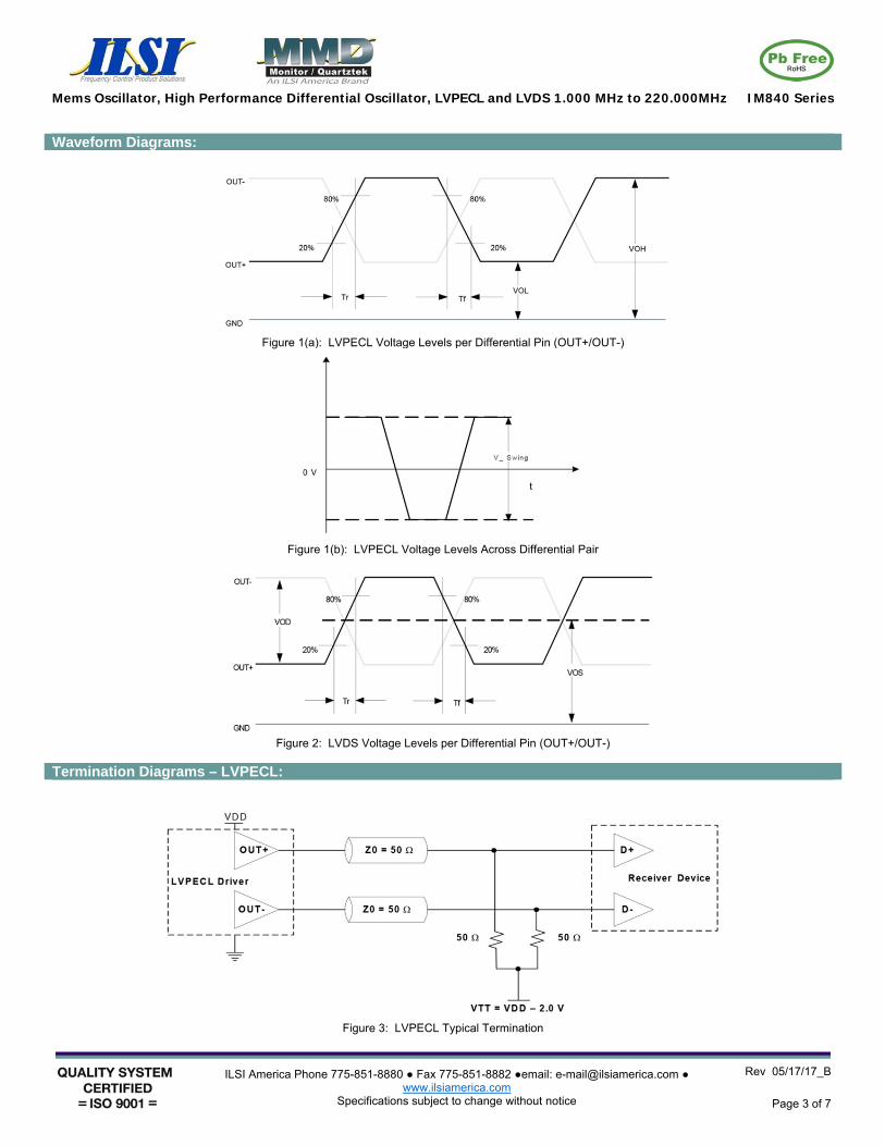
Waveform Diagrams:
Figure 1(a): LVPECL Voltage Levels per Differential Pin (OUT+/OUT-)
Figure 1(b): LVPECL Voltage Levels Across Differential Pair
Figure 2: LVDS Voltage Levels per Differential Pin (OUT+/OUT-)
Termination Diagrams – LVPECL:
Figure 3: LVPECL Typical Termination
Mems Oscillator, High Performance Differential Oscillator, LVPECL and LVDS 1.000 MHz to 220.000MHz IM840 Series
ILSI America Phone 775-851-8880 Fax 775-851-8882 email: [email protected] www.ilsiamerica.com
Specifications subject to change without notice
Rev 05/17/17_B
Page 4 of 7
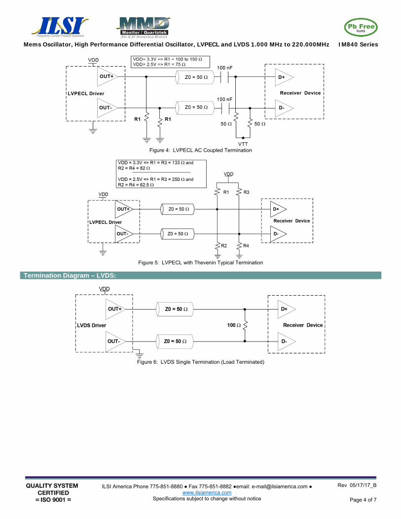
Figure 4: LVPECL AC Coupled Termination
Figure 5: LVPECL with Thevenin Typical Termination
Termination Diagram – LVDS:
Figure 6: LVDS Single Termination (Load Terminated)
Mems Oscillator, High Performance Differential Oscillator, LVPECL and LVDS 1.000 MHz to 220.000MHz IM840 Series
ILSI America Phone 775-851-8880 Fax 775-851-8882 email: [email protected] www.ilsiamerica.com
Specifications subject to change without notice
Rev 05/17/17_B
Page 5 of 7
Environmental Specifications:
Environmental ComplianceParameter Condition/Test Method
Mechanical Shock MIL-STD-883F, Method 2002
Mechanical Vibration MIL-STD-883F, Method 2007
Temperature Cycle JESD22, Method A104
Solderability MIL-STD-883F, Method 2003
Moisture Sensitivity Level MSL Level 1 at +260ºC
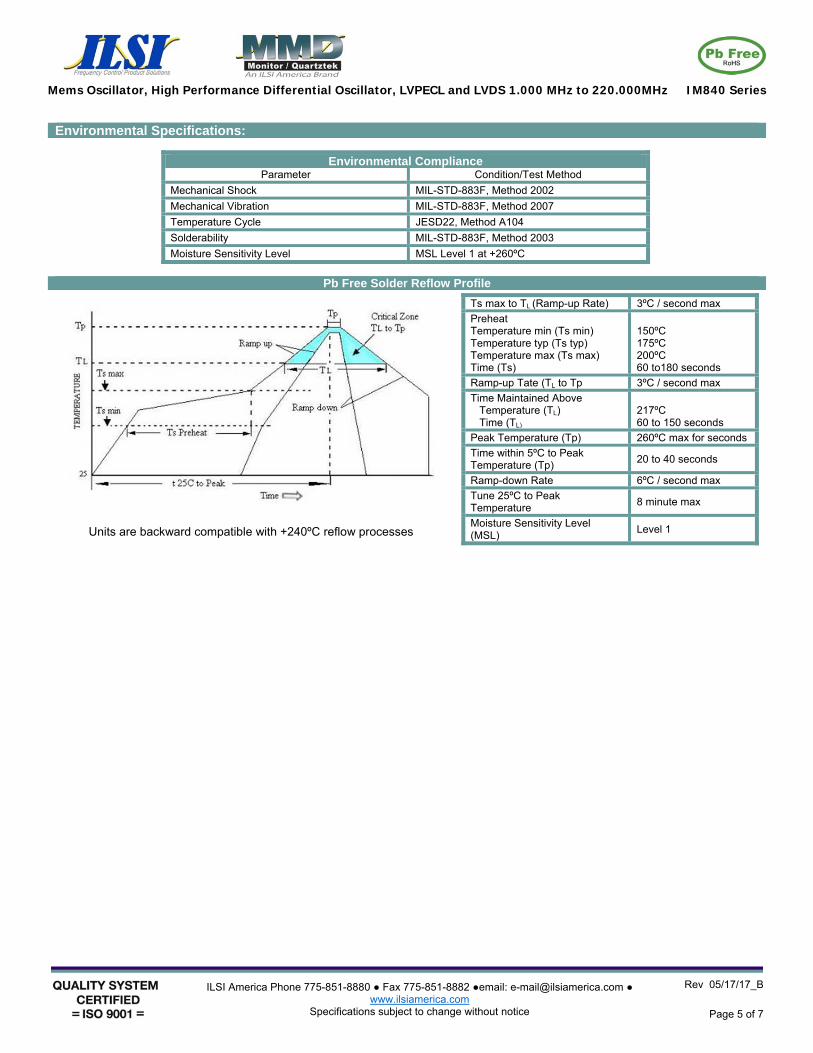
Pb Free Solder Reflow Profile
Ts max to TL (Ramp-up Rate) 3ºC / second max
Preheat Temperature min (Ts min) Temperature typ (Ts typ) Temperature max (Ts max) Time (Ts)
150ºC 175ºC 200ºC 60 to180 seconds
Ramp-up Tate (TL to Tp 3ºC / second max
Time Maintained Above Temperature (TL) Time (TL)
217ºC 60 to 150 seconds
Peak Temperature (Tp) 260ºC max for seconds
Time within 5ºC to Peak Temperature (Tp)
20 to 40 seconds
Ramp-down Rate 6ºC / second max
Tune 25ºC to Peak Temperature
8 minute max
Moisture Sensitivity Level (MSL)
Level 1
Units are backward compatible with +240ºC reflow processes
Mems Oscillator, High Performance Differential Oscillator, LVPECL and LVDS 1.000 MHz to 220.000MHz IM840 Series
ILSI America Phone 775-851-8880 Fax 775-851-8882 email: [email protected] www.ilsiamerica.com
Specifications subject to change without notice
Rev 05/17/17_B
Page 6 of 7
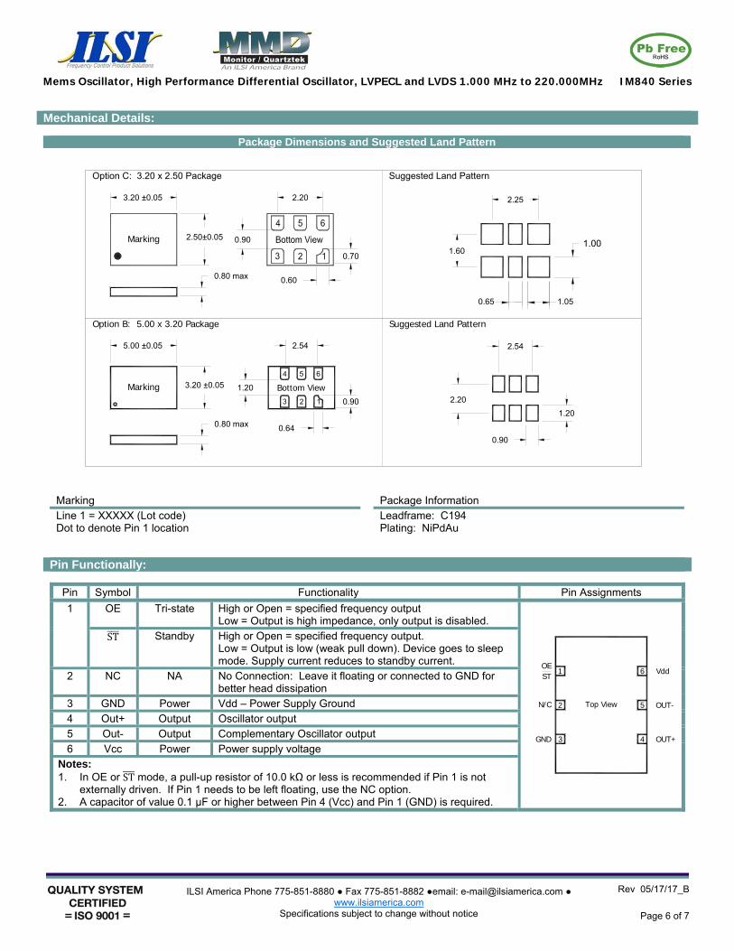
Mechanical Details:
Package Dimensions and Suggested Land Pattern
Marking
5.00 ±0.05
3.20 ±0.05 1.20
2.54
0.64
0.90
0.80 max
2.54
2.20
0.90
1.20
Bottom View
54 6
23 1
Option B: 5.00 x 3.20 Package Suggested Land Pattern
1.00
3.20 ±0.05
2.50±0.05 0.90
2.20
0.60
0.70
0.80 max
2.25
1.60
1.05
Option C: 3.20 x 2.50 Package Suggested Land Pattern
0.65
Marking
Marking
Line 1 = XXXXX (Lot code) Dot to denote Pin 1 location
Package Information
Leadframe: C194 Plating: NiPdAu
Pin Functionally:
Pin Symbol Functionality Pin Assignments
1 OE Tri-state High or Open = specified frequency output Low = Output is high impedance, only output is disabled.
1 6
43
Top View
GND
Vdd
OUT+
OEST
2 5 OUT-N/C
ST Standby High or Open = specified frequency output. Low = Output is low (weak pull down). Device goes to sleep mode. Supply current reduces to standby current.
2 NC NA No Connection: Leave it floating or connected to GND for better head dissipation
3 GND Power Vdd – Power Supply Ground
4 Out+ Output Oscillator output
5 Out- Output Complementary Oscillator output
6 Vcc Power Power supply voltage Notes: 1. In OE or ST mode, a pull-up resistor of 10.0 kΩ or less is recommended if Pin 1 is not
externally driven. If Pin 1 needs to be left floating, use the NC option. 2. A capacitor of value 0.1 µF or higher between Pin 4 (Vcc) and Pin 1 (GND) is required.
Mems Oscillator, High Performance Differential Oscillator, LVPECL and LVDS 1.000 MHz to 220.000MHz IM840 Series
ILSI America Phone 775-851-8880 Fax 775-851-8882 email: [email protected] www.ilsiamerica.com
Specifications subject to change without notice
Rev 05/17/17_B
Page 7 of 7
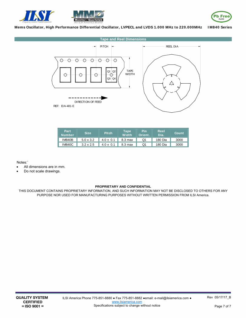
Tape and Reel Dimensions
DIRECTION OF FEEDREF: EIA-481-E
Q3 Q4
Q2Q1WIDTHTAPE
PITCH REEL DIA
Part Number Size Pitch Tape
Width Pin
Orient.Reel Dia. Count
IM840B 5.0 x 3.2 4.0 ± 0.1 8.3 max Q1 180 Dia 3000 IM840C 3.2 x 2.5 4.0 ± 0.1 8.3 max Q1 180 Dia 3000
Notes:` All dimensions are in mm. Do not scale drawings.
PROPRIETARY AND CONFIDENTIAL THIS DOCUMENT CONTAINS PROPRIETARY INFORMATION, AND SUCH INFORMATION MAY NOT BE DISCLOSED TO OTHERS FOR ANY
PURPOSE NOR USED FOR MANUFACTURING PURPOSES WITHOUT WRITTEN PERMISSION FROM ILSI America.