Embed Size (px)
Citation preview

MEMS Solution for Semiconductor ProbingMEMS Solution for Semiconductor Probing
SouthSouth--Western Testing Workshop PresentationWestern Testing Workshop Presentation
矽晶源高科股份有限公司SCS Hightech Inc.
Presented by Dr. Howard Hsu06-06-2005
22
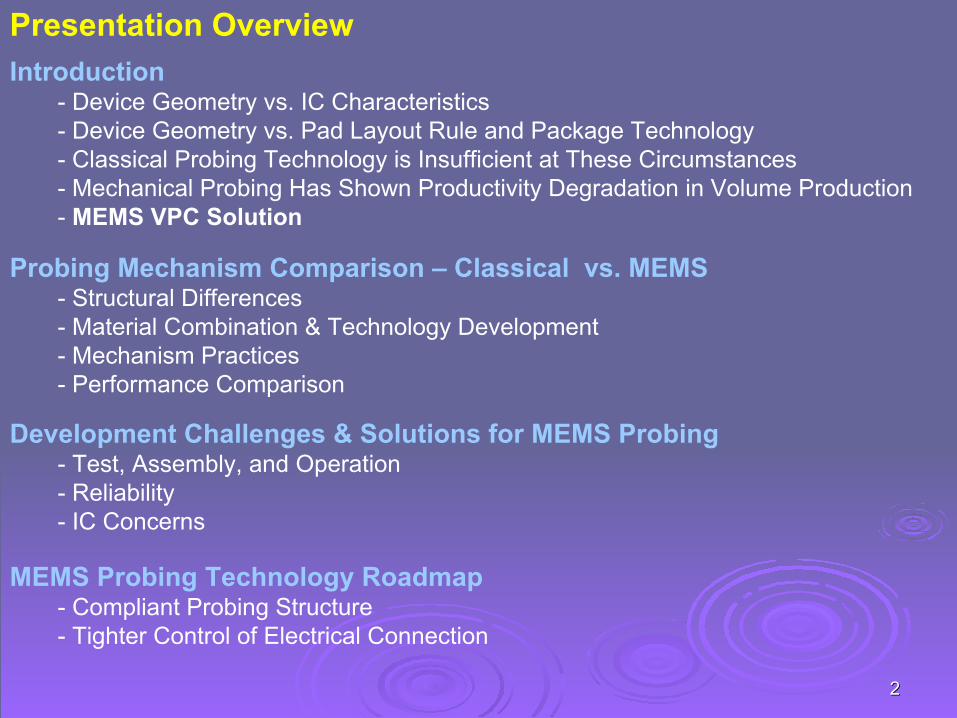
Presentation Overview
MEMS Probing Technology Roadmap- Compliant Probing Structure- Tighter Control of Electrical Connection
Introduction- Device Geometry vs. IC Characteristics- Device Geometry vs. Pad Layout Rule and Package Technology- Classical Probing Technology is Insufficient at These Circumstances- Mechanical Probing Has Shown Productivity Degradation in Volume Production- MEMS VPC Solution
Probing Mechanism Comparison – Classical vs. MEMS- Structural Differences- Material Combination & Technology Development- Mechanism Practices- Performance Comparison
Development Challenges & Solutions for MEMS Probing- Test, Assembly, and Operation - Reliability - IC Concerns

MEMS Solution for Semiconductor ProbingMEMS Solution for Semiconductor ProbingIntroductionIntroduction

44
IntroductionDevice Geometry vs. IC Characteristics
KGDKGD
Wafer Level Burn InWafer Level Burn In
I/O pins over 1000I/O pins over 1000High speed testHigh speed testBurnBurn--in and test before packagein and test before package
Vertical Probe CardVertical Probe CardTestingTesting測試測試
PbPb--Free Solder BumpFree Solder Bump
Unferfill Development Unferfill Development
Materials, Reliability, MCMMaterials, Reliability, MCMCOBCOBBBULBBUL
Flip Chip PackageFlip Chip PackagePackagePackage封裝封裝
Number of transistors Number of transistors ––Increase Increase
Speed greater than 300 MHzSpeed greater than 300 MHz
Number of function, I/O, power, and Vdd & Vss are Number of function, I/O, power, and Vdd & Vss are increasing.increasing.Speed faster than 300 MHz, package no wire bond.Speed faster than 300 MHz, package no wire bond.Number of I/Os increases too fast, therefore Array Number of I/Os increases too fast, therefore Array Design is the major trend.Design is the major trend.
Power Power –– Increase Increase ComponentsComponents元件元件
Smaller transistor, large quantity, faster speed.Smaller transistor, large quantity, faster speed.Stepper / Photo down to 0.065 Stepper / Photo down to 0.065 umum
Low leakage, capacitor effects, thermal conductivity, Low leakage, capacitor effects, thermal conductivity, power consumption, and higher integration ability.power consumption, and higher integration ability.
Low k Low k –– dielectric ~ 2.2dielectric ~ 2.2
Low power consume & voltage, Energy storageLow power consume & voltage, Energy storageSOI CapacitorSOI Capacitor
Low Resistance & Electronic migrationLow Resistance & Electronic migrationHigh conductivity & Thermal ConductivityHigh conductivity & Thermal Conductivity
Copper ProcessCopper ProcessProcess Process TechnologyTechnology製程技術製程技術
Remarks Remarks 備註備註20032003--20052005

55
IntroductionDevice Geometry vs. Pad Layout Rule and Package Technology
Device Technology is going further…
IC Pad Layout Rule is getting more and more critical…
Package Technology has to be changed in order to fit the progress…
Flip chip packageWire Bonding Package
Pad Pitch over 200um Pad Pitch over 200um Pad Pitch under 100um
Above 0.35um~2000
0.35um ~ 0.18um2000~2002
0.18um ~ 0.13um2002~2004
0.13um below2004~
Linear Bump Design Stagger Bump Design Array Bump Design

66
IntroductionClassical Probing Technology is Insufficient at These Circumstances
• Array Bump Probing
- Bump pitch will need to go lower than 150um- Maintenance free probe card- No burning tips- Short lead-time for order delivery- Consistent probing; no need to re-probe- High frequency probing
• Aluminum Pad Probing
- Multiple sites- Small pad pitch ~ 50um

77
Results huge customer service efforts!!!
IntroductionMechanical Probing Has Shown Productivity Degradation in Volume Production
Long repair time
Burning Tips
Pad Scratch Low probing life
Results a higher cost and lower efficiency!!!
Long offline cleaning
Low productivity
Higher noise Expensive rework

88
IntroductionMEMS VPC Solution
MEMS Prove Card SpecificationsMEMS Prove Card Specifications
2 ohm whole path2 ohm whole pathPath ResistancePath Resistance
Nickel, Copper, and SilverNickel, Copper, and SilverMajor MaterialMajor Material
Smaller than 10nA at 5 voltsSmaller than 10nA at 5 voltsLeakageLeakage
50 ohm plus minus 5 ohm50 ohm plus minus 5 ohmImpendence MatchImpendence Match
< 2 weeks< 2 weeksRepeat order LTRepeat order LT
6~8 weeks (design related)6~8 weeks (design related)11stst order Leadorder Lead--timetime
100g / pin100g / pinShear ForceShear Force
1 A1 AMax. CurrentMax. Current
< 1.5um< 1.5umPlanarityPlanarity
1um1umAccuracy Accuracy
120um array, 35um LDI120um array, 35um LDIMin. Probing PitchMin. Probing Pitch
0 ~ 4 inch0 ~ 4 inchMax. Probing AreaMax. Probing AreaUp to 100umUp to 100umProbe Tip HeightProbe Tip Height
8 ~ 12 um8 ~ 12 umProbe Tip Probe Tip DimensionDimension
Vertical Probe card for Aglient 93000
Vertical Probe Card for Cadence Type
Here is the solution!!

MEMS Solution for Semiconductor ProbingMEMS Solution for Semiconductor Probing
Probing Mechanism Comparison Probing Mechanism Comparison –– Classical vs. MEMSClassical vs. MEMS

1010
Probing Mechanism Comparison – Classical vs. MEMSStructure Differences
Classical Vertical Type Probe Card- Probing tip will deform cause open issue- Use PCB substrate- Need cleaning both online and offline
MEMS Vertical Type Probe Card- Rigid tip will never deform- Use ceramic substrate- Excellent co-planarity w/o manual adjustment- No cleaning, no re-probing, and no repairing

1111
Probing Mechanism Comparison – Classical vs. MEMSMaterial Combination
Automated Layout
Nickel Tip
CopperContact Pads
Copper RDL
LTCC Substrate
Inter-relation of all process parameters: Chemicals, Temp., Plasma, double side process…. etc
Ceramic Substrate
RDLVia Area
Tip
Contact Pads
Material content of each part

1212
Probing Mechanism Comparison – Classical vs. MEMSTechnology Development
10um
50um
Classical VPC:Use the mechanical technology – minimum pitch is ~150um for array VPC
MEMS VPC: Use the same process to fabricate the sub-micron level rigid tips.Can be applied to small pitch ~35um multiple die sorting.

1313
Probing Mechanism Comparison – Classical vs. MEMSTechnology Development
Use the same process technology to fabricate the sub-micron level rigid tips for LCD driver IC probing.
45um
The 45um pitch rigid tip of dual-site LCD Driver IC probe card photo under microscope.
1414
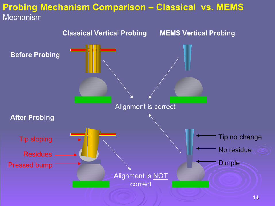
Probing Mechanism Comparison – Classical vs. MEMSMechanism
Before Probing
After Probing
Classical Vertical Probing MEMS Vertical Probing
Pressed bumpResidues
Tip sloping
Dimple
No residue
Tip no change
Alignment is correct
Alignment is NOTcorrect

1515
Probing Mechanism Comparison – Classical vs. MEMSPerformance
2 weeks2 weeks4 weeks4 weeksVolume lead timeVolume lead timeRepeat orderRepeat order
Tip cleaningTip cleaning
ReprobingReprobing
LDI probingLDI probing
Multiple Site Multiple Site ProbingProbing
Volume lead timeVolume lead timeFirst orderFirst order
Pad PitchPad Pitch
Bumped pad only Bumped pad only for nowfor nowDepends on pad pitchDepends on pad pitch
5 ~ 6 weeks5 ~ 6 weeks6 ~ 8 weeks6 ~ 8 weeks
Under 120 umUnder 120 um> 150 um> 150 um
No need, nor online maintenanceNo need, nor online maintenanceNeed, because residueNeed, because residue
No needNo needNeedNeed
Already in evaluation sampleAlready in evaluation sampleNot available (other types, Not available (other types, such as cantilever)such as cantilever)
SCS Diamond Vespa SCS Diamond Vespa MEMS VPCMEMS VPC
Classical C type Probe CardClassical C type Probe Card
Comparison Table for different probe card

1616
Probing Mechanism Comparison – Classical vs. MEMSPerformance
0
0.5
1
1.5
2
2.5
3
100
250
350
450
550
625
Freq2 (MHz)
Leve
l (V) Step 1
Step 2Step 3
C type
SCS
Tester internal signal quality
MEMS Vertical Probe Card:Has passed several qualifications in Taiwan. Electrical performance (up to 3GHz) is superior to classical manufactured probe cards.

MEMS Solution for Semiconductor ProbingMEMS Solution for Semiconductor ProbingDevelopment Challenges & Solutions For MEMS ProbingDevelopment Challenges & Solutions For MEMS Probing

1818
Probing PressureAbout ~25g per tip with our tip head size.
Tip shapeLong neck cone shape for non-uniformity of the bumps.
TestingAlignment focus issues – tip head is 10umSOP training for using MEMS probe card.
Load BoardParallelism between PCB and LTCCRequires high stand-off.
Development Challenges & Solutions For MEMS ProbingTest, Assembly, and Operation
Chuck
Load Board
Tester Head UnitTester
Solder Bump
Wafer

1919
Durability for Probing ICs
Excellent probing consistency (eliminate re-probing)Excellent probing life time – some model probed over 1.3M, other around 1M.Excellent maintenance – No need to repair anymore because lead time is short.
Before After 150K times After 350K times
Result:- With clean process, the wear out rate is around 3~6 um after 12k times. - Probe without clean process, there is almost no wear out (pin-height) after 350k insertions.
Subject: SCS MEMS VPC for 8” wafers(633 pins)Tester/Prober: Agilent 93000/P600, P12/TELClean sheet: Enhanced 3M type C (type C + polish paper/pink type)Tool: Olympus microscope with micro meterReading: Check pin high twice( from ULTCC to tip) for average.
Development Challenges & Solutions For MEMS ProbingReliability

2020
Rigid TipAfter the tip probes into the bump, it will produce a “dimple” that looks like a crater.
DimpleThis has been notified and IC has also been checked out with reliability qualification.
Development Challenges & Solutions For MEMS ProbingIC Concerns
Dimple ReliabilityThe reliability issue has been passed by a famous Taiwan foundries and packaging house.

MEMS Solution for Semiconductor ProbingMEMS Solution for Semiconductor Probing
MEMS Probing Technology RoadmapMEMS Probing Technology Roadmap

2222
MEMS Probing Technology RoadmapCompliant probing structure
Chuck
Load Board
Tester Head UnitTester
Solder Bump
Wafer
Ceramic
Rigid Tip
WaferAluminum PadThin-film RDL
To control the tip pressureNew material needed!! For aluminum pads!!
Compliant layer

2323
MEMS Probing Technology RoadmapCompliant probing structure
wafer
Ceramic
Compliant layerTo provide adjustment for improving contact uniformity.
wafer wafer wafer
This layer is soft, reform while the pressure applied.
Aluminum Pads

2424
MEMS Product R&D RoadmapTighter Control of Electrical Connection – Ceramic Section
Improvement of the LTCC to improve the performance of the probe card
Layer 1
Layer 2
Layer 3
Layer 4
Layer 5
Layer N
Backside Output
Tape Thickness ~ 200umafter co-fired
Line Thickness < 10umafter co-fired
Ground Thickness <10 um after co-fired
Printing
Line width 75um Center to Center 125um
Catch Pad 75um

2525
Q & AEnd of Presentation
SCS Hightech Inc. Website: http://www.scs.com.tw/, TEL +886-3-349-8999, FAX +886-3-346-8998, 2005 All Rights Reserved.


![INTRODUCTION€¦ · Web viewThey have been used in a range of applications [1], including MEMS capacitors [2], interconnectors [3], electromechanical probing [4] and MEMS switches](https://img.pdfslide.net/doc/110x75/5f68478e3b13fc692c5ce056/introduction-web-view-they-have-been-used-in-a-range-of-applications-1-including.jpg)