Embed Size (px)
Citation preview
1
MEMS Testing and Metrology
International Workshop at
Messe Dresden, Saal Erlwein, October 9, 2013
2
Agenda 08:20 Welcome and Introduction
Dr. Heinrich Steger, Polytec
08:30 "Microelectronic Packaging Testing using CMOS MEMS Sensors"
Prof. Dr. Oliver Paul, IMTEK, Freiburg, Germany
09:00 "Multi-Physics Microsystems Testing and Modeling"
Dr. Xavier Rottenberg, IMEC, Belgium
09:30 "Interferometry of AlN-based microcantilevers: from the material properties and failure
mechanisms to the evaluation of reliability issues"
Prof. Dr. Christophe Gorecki, FEMTO-ST, Besancon, France
10:00 "What optics can do for the inspection of micro and nano components?"
Prof. Dr. Wolfgang Osten, Universität Stuttgart, Germany
10:30 - 11:00 Coffee Break
11:00 "Analysis of RF MEMS switches with metal‐metal contacts"
Dr. Steffen Kurth, Fraunhofer ENAS, Chemnitz, Germany
11:30 “Characterization of mechanical and electrical properties of RF-MEMS switches in BiCMOS
BEOL technology”,
Matthias Wietstruck, IHP, Frankfurt/Oder, Germany
12:00 “Wafer Prober – Characterization of MEMS devices on Wafer-Level”
Sebastian Giesmann, Cascade Microtech GmbH, Sacka, Germany
12:30 "Rapid measurements of 3D vibrations on microscopic structures"
Dr. Christian Rembe, Polytec, Waldbronn, Germany
13:00 - 14:00 Lunch
14:00 "Measurement of vibration, deformation and thermal response of microscopic components"
Prof. Dr. Shuji Tanaka, Tohoku University, Sendai, Japan
14:30 "MEMS Microbolometer Characterization and Modelling"
Fabian Utermoehlen, Robert Bosch GmbH, Gerlingen-Schillerhöhe, Germany
15:00 "Cryogenic measurements of advanced technology SiGe, IIIV and Carbon Nanotube transistors"
Paulius Sakalas, Technical University Dresden, Dresden, Germany
15:30 - 16:30 Coffee Break
16:00 "Testing Needs and Metrology Requirements from the Viewpoint of a MEMS-Fab"
Uwe Schwarz, X-FAB MEMS Foundry GmbH, Erfurt, Germany
16:30 "Measurement of contact resistance in magnetically operated devices (REED switches and MEMS)"
Sergey Karabanov, RMCIP, Ryazan State Radio Engineering University, Ryazan, Russia
17:00 "Dynamic Testing MEMS Gyro at Wafer Level"
Hugh Miller, SOLIDUS Technologies, Colorado Springs, USA
17:30 "Vibrometry in the field of MEMS - from stress detection in packaged membranes to functionality
tests of RF resonators",
Steffen Michael, IMMS, Ilmenau, Germany
3
Microelectronic Packaging Testing using CMOS MEMS Sensors
Oliver Paul
Department of Microsystem Engineering (IMTEK), University of Freiburg, Germany
E-mail: paul imtek.de
Abstract
Microelectromechanical systems (MEMS) fabricated using standard complementary metal oxide
semiconductor (CMOS) technology have many advantages, such as the excellent reproducibility and
small achievable size of the MEMS structures and their easy integration with microelectronic
circuitry. Mechanical CMOS test chips developed by the speaker’s group allow the spatial distribution
of the mechanical stress on the test chip surface to be measured. Once processed using
microelectronic packaging methods, the test chips provide in-situ information on the stress state of
the package. Thereby they offer a valuable tool for the monitoring and optimization of
microelectronic packaging processes. We report on high-density ball grid arrays, on the
encapsulation of thin chips, and on the thermomechanical stress contributed by molding materials.
The sensor systems used for the experiments include global and high-resolution arrays with up to
1700 microsensors sensitive to the six components of the mechanical stress tensor. Support by Intel,
Hillsboro, and Micronas, Freiburg, is gratefully acknowledged.
Short Biography
Oliver Paul received the Diploma degree in physics in 1986 and the D.Sc. degree in 1990 from the
ETH Zurich, Switzerland. After postdoctoral work at the Fraunhofer Institute for Solar Energy
Systems, he joined the Physical Electronics Laboratory at ETH Zurich in 1992 as a Lecturer and Group
Leader. Since 1998, he has been a Full Professor at the University of Freiburg, Germany, where he
heads the Laboratory for Microsystem Materials at the Department of Microsystems Engineering
(IMTEK). He is a coauthor of more than 300 technical publications, patents, and books. His group’s
research focuses on MEMS materials and fabrication technologies, physical microtransducers, and
microstructures for industrial and life science applications. Oliver Paul is a member of the Editorial
Boards of Sensors and Actuators A: Physical and Journal of Micromechanics and Microengineering,
and of the Editorial Advisory Board of the IEEJ Transactions on Electrical and Electronic Engineering.
He is a cofounder of Sensirion AG and Atlas Neuroengineering and cochaired the IEEE MEMS 2004
Conference in 2004. From 2006 to 2008, he has served as the Director of IMTEK. He is a founding
director of the German excellence cluster BrainLinks-BrainTools at the University of Freiburg.
4
Multi-Physics Microsystems Testing and Modeling
Xavier Rottenberg, imec, Belgium
E-mail: xrottenb imec.be
Abstract
Microsystems and Nanosystems operating in various physical domains and environments present
increasingly complex modeling as well as testing challenges. The purpose of this presentation is to
introduce these challenges through various test cases and the testing solutions implemented. The
importance of the close interaction between modeling and testing will be highlighted.
Short Biography
Xavier Rottenberg was born in Brussels, Belgium, in April 1976. He received the M.S. degree in
physics engineering and the supplementary degree in theoretical physics from the Université Libre de
Bruxelles, Brussels, in 1998 and 1999, respectively. He received in 2008 his Ph.D. degree in Elec. Eng.
From the Katholieke Universiteit Leuven, Leuven, Belgium.
He worked one year at the Royal Meteorological Institute of Belgium in the field of remote sensing
from space. He joined imec, Division of Microsystems, Components and Packaging (MCP), Leuven, in
2000, where he contributed to research in the field of RF-MEMS, modelization, and integration. He
now leads the Microsystems Design and Modeling team at imec specializing in multi-physics
applications, e.g. inertial measurement units, atmospheric plasma devices, ultrasound transducers,
photonic and phononic devices. He has coauthored over 40 international scientific
journal/conference papers in the area of (RF-)MEMS devices and circuits and has been issued patents
in these fields.
5
Interferometry of AlN-based microcantilevers: from the material properties and failure
mechanisms to the evaluation of reliability issues
Christophe Gorecki, FEMTO-ST, Besancon, France
E-mail: christophe.gorecki femto-st.fr
Abstract
Micro-electro-mechanical systems are exposed to a variety of environmental stimuli, making a
prediction of operational reliability difficult. Here, we investigate environmental effects on properties
of piezoelectrically actuated microcantilevers, where AlN is used as actuation material. The
environmental effects to be considered include thermal and humid cycling, as well as harsh electrical
loading performed under normal conditions. Investigated properties are defined for the static and
dynamic behavior of microcantilevers. A Twyman-Green interferometer, operating in both
stroboscopic regime and time-average interferometry mode, is used as a metrology tool. The initial
deflection and frequency changes of the first resonance mode of the microcantilevers are monitored
during accelerated thermal aging tests, humidity tests, as well as harsh electrical loading and fatigue
tests. Finally, the resonant fatigue tests accelerated by application of a high voltage are accomplished
to evaluate a lifetime of microcantilevers. Monitoring the micromechanical behaviors of devices
driven by AlN during the lifetime tests assists monitoring of their long-term stability. FEM calculation
is used to identify critical areas of stress concentration in the cantilever structure and to further
explain various failure mechanisms.
Short Biography
Prof. Christophe Gorecki isa Director of Research CNRS (DR1 CNRS) at FEMTO-ST. He received the
Ph.D. in Optics at the University of Besançon in 1983 and joined Laboratoire d’Optique P.M. Duffieux
(LOPMD) as a CNRS Scientist. His research interests included optical inspection and micro-
measurements, applications of image processing techniques in optical metrology and Optical Pattern
Recognition methods. From 1995 to 1998 he joined for 3 years the University of Tokyo where he was
involved in research and development of Optical MEMS. Back to LOPMD he conducts research in
novel MOEMS architectures for micro- and nanosensors as well as development of metrology
methods for characterization of MOEMS/MEMS. C. Gorecki has supervised many national projects
and several European projects. He has more than 160 technical papers to his credit and 3 book
chapters. From 1992 to 1995 C. Gorecki served as national Secretary of the French Society of Optics
(SFO). He is also a Fellow of the SPIE and member of the Board of Directors of SPIE. He is the
President of the European Associated Laboratory in Microtechniques « LEA-µT » including FEMTO-ST
and EPFL Lausanne. From 2007 to 2009, Prof.Gorecki was a member and expert of Disciplinary
Committee of French ANR for programs Blanc and Jeunes Chercheurs. He received in 2012 the prize
of European Optical Society.
6
What Optics can do for the Inspection of Micro and Nano Components?
Wolfgang Osten
Institut für Technische Optik, Universität Stuttgart, Pfaffenwaldring 9, D-70569 Stuttgart, Germany
E-mail: osten ito.uni-stuttgart.de
Keywords: optical metrology, advantages, limitations, high resolution metrology, defectoscopy, cd-
metrology, experimental stress analysis, non-destructive testing, material parameters, calibration
samples, sensor fusion
Abstract
Optical metrology has shown to be a versatile tool for the solution of many measurement
and inspection tasks. The main advantages of optical methods are the non-contact nature, the non-
destructive and areal working principle, the fast response, flexible scalability, high sensitivity,
resolution and accuracy. Consequently, optical principles are increasingly being considered in many
areas where reliable data about the shape, the surface properties, the stress state and the strength
of the object under test have to be measured. However, these advantages must be paid with some
serious disadvantages that are mainly connected with the unpleasant properties of identification
problems and the high sensitivity of optical methods against environmental influences.
In this contribution several examples are presented where optical metrology can be helpful
for the inspection of micro and nano components. The presentation is focused on two topics:
- the discussion of the potential and the limitations of optical inspection technologies and the
resulting challenges, and
- the discussion of modern inspection technologies that refer to these challenges.
The given examples relate to both the inspection of MEMS as well semiconductor nano structures.
Short Biography
Wolfgang Osten received the MSc/Diploma in Physics from the Friedrich-Schiller-University Jena in
1979. From 1979 to 1984 he was a member of the Institute of Mechanics in Berlin working in the
field of experimental stress analysis and optical metrology. In 1983 he received the PhD degree from
the Martin-Luther-University Halle-Wittenberg for his thesis in the field of holographic
interferometry. From 1984 to 1991 he was employed at the Central Institute of Cybernetics and
Information Processes ZKI in Berlin making investigations in digital image processing and computer
vision. Between 1988 and 1991 he was heading the Institute for Digital Image Processing at the ZKI.
In 1991 he joint the Bremen Institute of Applied Beam Technology (BIAS) to establish and to direct
the Department Optical 3D-Metrology till 2002. Since September 2002 he has been a full professor at
the University of Stuttgart and director of the Institute for Applied Optics. From 2006 till 2010 he was
the vice rector for research and technology transfer of the Stuttgart University where he is currently
an elected member of the university council. His research work is focused on new concepts for
industrial inspection and metrology by combining modern principles of optical metrology, sensor
technology and image processing. Special attention is directed to the development of resolution
enhanced technologies for the investigation of micro and nano structures.
7
Analysis of RF MEMS switches with metal‐metal contacts
Steffen Kurth, Fraunhofer ENAS
E-mail: Steffen.Kurth enas.fraunhofer.de
Abstract
This contribution reports on the analysis of metal-metal contacts of MEMS switches. A novel
high aspect ratio MEMS fabrication sequence in combination with wafer level packaging is applied
for fabrication of an RF MEMS switch with lateral motion. It allows for a relatively large actuation
electrode area in a small package, and for high actuation force even with an actuation voltage of 5 V.
The focus of this contribution is on the contact behavior. It is shown how operation conditions as like
as actuation voltage, RF power, and DC bias influence the contact resistance. The power handling
capability and its influence on the contacts, and the intermodulation were investigated and reported
as well.
Short Biography
Steffen Kurth received the Diploma in electrical engineering and the Dr.-Ing. degree in MEMS
modeling and experimental characterization from Chemnitz University of Technology, Chemnitz,
Germany, in 1991 and 1995, respectively. He was a Lecturer with Chemnitz University of Technology
and supervised more than 30 graduate students for Diploma and Dr.-Ing. degrees. Since 2001, he has
been with the Fraunhofer Institute for Reliability and Microintegration and Fraunhofer Institute for
Electronic Nano Systems (ENAS), Chemnitz, and has been active in the fields of design and test of
MEMS-component-like accelerometers, vacuum pressure sensors, scanning mirrors, tunable infrared
filters, and other microoptoelectromechanical system components. He is currently leading the MEMS
Test Group, Fraunhofer ENAS, managing several joint research and development projects. His current
research interests include the development of micro- and nanostructured components for
microoptoelectromechanical systems and radio-frequency MEMSs.
8
Characterization of Mechanical and Electrical Properties of
RF-MEMS Switches in BiCMOS BEOL Technology
M. Wietstruck, M. Kaynak, B. Tillack
IHP – Innovations for High Performance Microelectronics
Im Technologiepark 25, 15236 Frankfurt (Oder), Germany
E-mail: wietstruck ihp-microelectronics.com
Abstract
This paper describes the characterization and optimization of mechanical and electrical properties of
an embedded RF-MEMS switch integrated in a 0.25 µm BiCMOS technology by use of laser doppler
vibrometry and white light interferometry. In combination with a temperature-controlled semi-
automated probe-station, optical MEMS characterization on wafer-level allows for fast and cost-
efficient RF-MEMS switch performance analysis and optimization. It provides a deep understanding
of electromechanical behavior which is mandatory for process and design optimization, long-term
reliability and circuit and system design integration.
Short Biography
M. Wietstruck finished his studies of microsystem technology in Berlin in 2009. Since 2010, he is
working at IHP in Frankfurt (Oder), Germany in the areas of RF-MEMS and Through-Silicon Via
integration. The goal of RF-MEMS integration is the monolithic integration of RF-MEMS in a BiCMOS
technology for frequencies up to 100GHz and above. His focus is on the mechanical and electrical
characterization of MEMS, design optimization using FEM simulation and reliability.
9
Wafer Prober – Characterization of MEMS devices on Wafer-Level
Sebastian Giessmann,
Cascade Microtech GmbH, Sacka, Germany
E-mail: Sebastian.Giessmann cmicro.com
Abstract
Wafer-probers are a proven platform for performing electrical tests on wafer level. For MEMS
devices the measurement only of the electrical behavior of is not sufficient. Non-electrical stimuli or
measurements of non-electrical behavior are beneficial or mandatory. This requires additional
modules. Several solutions for wafer-level characterization of MEMS devices like pressure sensors,
silicon microphones, RF switches or µBolometer have been developed and successful implemented
at numerous MEMS companies and research institutes. This presentation will give an overview about
existing field-proven wafer-level test solutions for MEMS devices.
Pressure sensors can be tested by applying static pressure to the device-under-test’s diaphragm
whiles measuring the resistance of the Wheatstone bridge. All these systems are based on three
main principles. First, the test pressure can be applied to the wafer’s backside by a unique chuck
system. Alternatively, pressure can be applied to the DUT from top by a proximity nozzle causing an
impact pressure. This method can be used for both, absolute and differential sensors. Finally, the
wafer-prober can be placed inside a pressurized chamber and operated from vacuum up to pressure
ranges above atmosphere.
An alternative method is the dynamic test of the membrane behavior by applying vibration and
detecting the resulting frequencies. This dynamic approach has been developed in multilateral
project of MEMUNITY partners from the MEMS industry, research institutes and test equipment
manufacturers.
Microphone membranes are acoustically stimulated. The response is measured by a probe card with
integrated reference microphone and evaluated by the acoustic test software.
A variety of MEMS can be tested inside a vacuum probe station before their packaging process. The
vacuum chamber provides the identical environment, e.g. controlled inert gas or vacuum, like the
future working environment of the device.
Short Biography
Sebastian Giessmann received his degree in Electrical Engineering from the Dresden University of
Applied Science in 1998. He started with SUSS MicroTec Test Systems as a software developer
involved in the development of new equipment for the semiconductor industry. For two years he
worked for MFI Technologies, a SUSS subsidiary based in San Jose, California on the development of
an innovative submicron wafer probe station based on the AFM principle. Since 2007, Sebastian has
been the application engineer responsible for the SUSS vacuum and cryogenic test systems and
MEMS test solutions. In January 2010, the SUSS test division was acquired by Cascade Microtech.
10
Rapid measurements of 3D vibrations on microscopic structures
Christian Rembe,
Polytec GmbH, Waldbronn, Germany
E-mail: C.Rembe Polytec.de
Abstract
This contribution addresses the recent progress in microscopic vibration analysis. During the last 15
years laser-Doppler vibrometry has become the state-of-the-art technique for detecting of out-of-
plane vibrations with picometer amplitude resolution on microscopic structures as, for example,
microelectromechanical systems (MEMS). The problem with laser-Doppler vibrometry is that the
displacement or velocity is detected only in direction of the measurement beam and, thus, three
impinging laser beams are necessary to investigate all components of a three-dimensional (3D)
motion. This requirement is not problematic for 3D-vibration measurements on macroscopic objects
with scattering surfaces but for reflective microstructures. A general problem of measuring 3D
vibrations with three laser beams is optical crosstalk. This problem is especially critical for MEMS
applications because the three beams have to be positioned closely to achieve high lateral
resolution. A spot of 35 µm diameter was the best achievement for a system designed to analyze
components in hard-disk drives. This solution is not suited for MEMS devices because structures with
sufficient size for equal scatter conditions and a uniform motion within the 35 µm spot are
necessary. Therefore, stroboscopic videomicroscopy has been employed successfully to MEMS to
study periodic in-plane vibrations. The drawbacks of this method are a “low” amplitude resolution
(roughly 10-100 nm) and a rather time-consuming measurement procedure. A real-time, broad-
bandwidth vibration spectrum with picometer resolution cannot be obtained with stroboscopic
videomicroscopy. Therefore, a new measurement technique which provides the performance of
laser-Doppler vibrometry also for in-plane and 3D-vibrations has been an important demand of the
MEMS community for many years. This talk discusses new techniques which allow to solving the
restrictions for in-plane-vibration measurements. The performance of a new 3D-vibration
microscope with a single laser beam that detects scattered light from different directions is discussed
and first measurements are shown.
Short Biography
Christian Rembe received the diploma in Physics from the University of Hanover, Hanover, Germany,
in 1994. From 1994 to 1999, he was a PhD student at the University of Ulm, Ulm, Germany where he
earned a doctor degree in Electrical Engineering. 1999 he joined the Berkeley Sensor&Actuator
Center at the University of California, Berkeley as postdoctoral, research engineer with support of a
Feodor-Lynen-Scholarship of the Alexander von Humboldt-Foundation and a UC Berkeley MacKay-
Lecturer Fellowship. Since 2001 he is working as Manager Development Optics at Polytec GmbH,
Waldbronn, Germany.
11
Measurement of vibration, deformation and thermal response
of microscopic components
S. Tanaka
Tohoku University, Sendai, Japan
E-mail: tanaka mems.mech.tohoku.ac.jp
Abstract This presentation mainly consists of two parts. The first part introduces some
examples of MEMS evaluation using Polytec optical analyzers. 1) The resonance modes of high
frequency piezoelectric MEMS resonators were observed by ultrahigh frequency laser Doppler
vibrometry. Complicated resonance mode shapes from a few ten MHz to several hundred MHz were
successfully obtained and compared with FEM simulation results. 2) A novel lateral type PZT actuator
was evaluated by strobe imaging. The fundamental resonance frequency was identified, and the
piezoelectric constant of composite PZT in deep Si trenches was calculated in conjunction with other
measurements. 3) The reliability in the hermeticity of wafer-level MEMS packaging was evaluated by
observing the deformation of pressure-sensitive diaphragms by white light interferometry. Excellent
packaging reliability of an anodically-bondable LTCC cap wafer was confirmed after −40 °C/+125 °C
thermal cycling test.
The second part introduces a novel microscale temperature measurement technique using a
temperature sensitive paint (TSP). The TSP generates visible luminescence at 610 nm by ultraviolet
excitation at 355 nm, and the strength of the luminescence is dependent on the temperature of the
TSP. The millisecond order high speed thermal behavior at microscale was clearly observed by a
stroboscopic method using the TSP. This technique is faster and cheaper than infrared imaging using
an infrared focal plane array.
Short Biography
Prof. Tanaka studied at the Department of Mechano-Informatics, Faculty of Engineering, The
University of Tokyo. In 1999 he received his Dr. Eng. at the Department of Engineering Synthesis,
Graduate School of Engineering, The University of Tokyo.
He started his professional carrier as Research Fellow at The Japan Society for the Promotion of
Science (JSPS). 2001 He became Assistant Professor at the Department of Mechatronics and Precision
Engineering, Tohoku University and 2003 Associate Professor at the Department of Nanomechanics,
Tohoku University. He is Selected Fellow at the Center for Research and Development Strategy, Japan
Science and Technology Agency (JST). From 2010 to 2011 he was Guest Professor at the Katholieke
Universiteit Leuven, Belgium and collaborated with IMEC. 2012 he became Deputy Director of the
Micro-Nanomachining Research and Education Center, Tohoku University. 2013 he bescme Professor
at the Department of Bioengineering and Robotics, Tohoku University.
Prof. Tanakas research activities are: Biomechanodevices, Micro electro mechanical systems (MEMS),
Micro/nanofabrication and integration technology.
He published over 500 papers including over 300 journal and international conference papers, 17
sections of book, he holds 10 patents plus over 40 filed patents and he gave 87 invited talks and
lectures in conferences and workshops. Prof Tanaka received 9 prizes including The Young Scientists’
Prize, The Commendation for Science and Technology by the Minister of Education, Culture, Sports,
Science and Technology (2009) and German Innovation Award, Gottfried Wagener Prize (2012).
12
MEMS Microbolometer Characterization and Modelling
Fabian Utermöhlen
Robert Bosch GmbH, Robert-Bosch-Platz 1, 70839 Gerlingen-Schillerhöhe, Germany
E-mail: fabian.utermoehlen de.bosch.com
Keywords: MEMS Microbolometer, electrothermal modeling, thermal imaging, pn-junction diode,
MEMS characterization
Abstract
Each object with a temperature above absolute zero emits electromagnetic radiation according to its
temperature and surface properties. This thermal radiation can be collected by infrared detectors for
imaging applications without the need of artificial or natural illumination of the scene. Since objects
at room temperature have their spectral peak emittance around a wavelength of 10 μm and thus in
the far infrared (FIR) region, these detectors are designed to operate in the 8 to 14 μm atmospheric
window where radiation absorption in the atmosphere is significantly reduced. In contrast to
cryogenic quantum detectors, microbolometers operate at room temperature and can be
manufactured by using fully CMOS compatible processes. This makes them excellent candidates for
low-cost thermal imaging systems which can be used for automotive as well as consumer
applications.
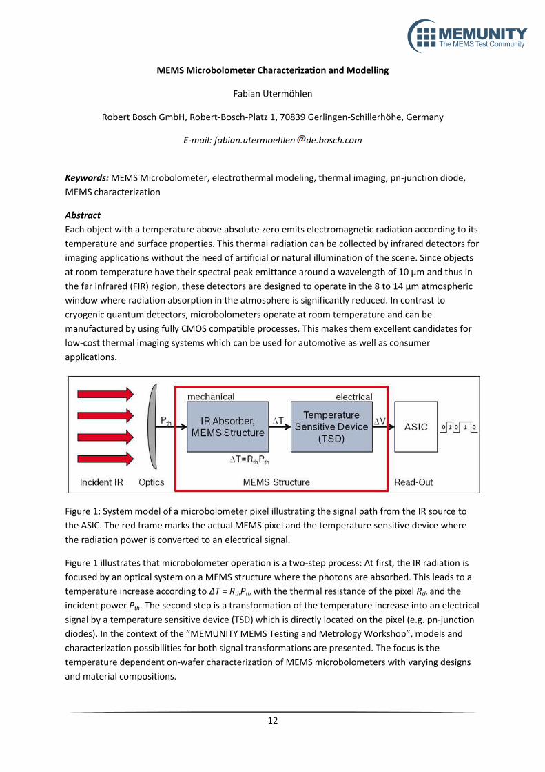
Figure 1: System model of a microbolometer pixel illustrating the signal path from the IR source to
the ASIC. The red frame marks the actual MEMS pixel and the temperature sensitive device where
the radiation power is converted to an electrical signal.
Figure 1 illustrates that microbolometer operation is a two-step process: At first, the IR radiation is
focused by an optical system on a MEMS structure where the photons are absorbed. This leads to a
temperature increase according to ΔT = RthPth with the thermal resistance of the pixel Rth and the
incident power Pth. The second step is a transformation of the temperature increase into an electrical
signal by a temperature sensitive device (TSD) which is directly located on the pixel (e.g. pn-junction
diodes). In the context of the ”MEMUNITY MEMS Testing and Metrology Workshop”, models and
characterization possibilities for both signal transformations are presented. The focus is the
temperature dependent on-wafer characterization of MEMS microbolometers with varying designs
and material compositions.
13
Short Biography
Fabian Utermöhlen was born in 1987 in Northeim, Germany. He received the Dipl.-Ing. Degree in
electrical engineering with focus on microelectronics from the Technische Universität Dresden,
Germany, in 2011. In the same year, he joined Robert Bosch GmbH, Gerlingen-Schillerhöhe,
Germany, where he is currently working towards his Ph.D. degree in cooperation with the University
of Stuttgart.
14
Cryogenic measurements of advanced technology SiGe, IIIV and Carbon Nanotube transistors
Paulius Sakalas1,2
1 CEDIC, IEE, Technische Universität Dresden, Mommsenstr. 13, 01062 Dresden, Germany 2 FRL, Semiconductor Physics Institute, Center for Physical Sciences and Technology, Goštauto 11,
01108 Vilnius, Lithuania
* Corresponding author: paulius.sakalas tu-dresden.de
Abstract
Recent InP DHBT and SiGe HBT process technology improvement has attracted an interest in
mm-wave and THz applications (e.g. [1],[2],[3]). InP DHBT and SiGe HBT have proven to be among
the fastest transistors today. Recently it was shown that 130 nm InP DHBT and 350 nm SHBT with
BVCE0 =3.5 V and 2.7 V, respectively, exhibit a maximum transit frequency fT exceeding 520GHz [4],
[5] and a maximum oscillation frequency fmax beyond 1THz [4]. Extremely scaled InP HBTs with 12.5
nm base and 55 nm collector yield a record fT= 765 GHz keeping still reasonable BVCE0=1.65 V [6]. It
was shown that a slight cooling of InP HBTs down to lattice temperature Ta = -55°C resulted in an
increase to fT= 845 GHz.
Despite worse BVCE0 and lower electron mobility compared to InP based HBTs, scaled SiGe
HBTs also show very promising behavior towards THz operation as (fT/fmax)=(300/500) GHz has
recently been achieved [7]. It was shown that cooled down SiGe HBT do not suffer from full carrier
freeze-out and can still operate even at 4 K [8], yielding an fT increase up to 1 THz [9] and very low
high frequency noise behavior [10]. Thus both InP DHBT and SiGe HBTs are good candidates for
extreme applications like space electronics.
As an alternative to Si and IIIV materials, carbon gained lot of attention as promising material
for semiconductor electronics. The high interest in using carbon nanotube (CNT) FETs (CNTFETs) in
advanced electronics is based on their unique 1D transport properties resulting in quasi-ballistic
transport, Coulomb blockade, Luttinger liquid behavior, high linearity [11], [12]. High carrier velocity,
together with the quasi 1D tube geometry, yield theoretically and experimentally a very low intrinsic
(quantum) capacitance per tube of CQST~60 aF/µm [13], giving fT beyond 110 GHz*µm in the ballistic
limit [14]. Along with higher fT, fmax and lower power dissipation compared to graphene FETs [14],
CNTFETs are very attractive devices for analog high frequency applications. Electron scattering has
been studied extensively for metallic tubes [15], [16] but less for semiconducting tubes: defects,
physical bends, acoustic-phonon scattering at low bias and zone boundary optical phonon scattering
at high bias [15]. The doping free fabrication procedure prevents from carrier freeze-out in CNTs and
broadens the possible application area starting from deep cryogenic Ta up to 573 K [18]. Investigation
of CNTFETs at cryogenic temperatures, including single tube transistor, enables a deeper
understanding of CNT transport properties to provide insights for improving device models [17] and
the application-oriented device behavior.
In this work a comparative analysis is given for I(V) and RF characteristics (including noise) of
InP DHBTs with fmax=350 GHz and of SiGe HBTs with fmax=500 GHz over a wide temperature range,
including the deep cryogenic region. I(V) characteristics at different Ta are modelled by compact
model. The observed (fT, fmax) trends are explained using the temperature dependence of diffusion
capacitances and trans-conductance. A broad-band frequency NFmin (1-50 GHz) is analyzed in terms
of intrinsic noise sources. Compact modelling in practical temperature ranges is employed to explain
15
results.
As an alternative and perspective technology a carbon single wall manufacturable nanotube
transistors are analyzed over Ta, including cryogenic temperatures. The DC, RF characteristics, high-
frequency noise factor of top-gated, single-wall, multi-tube multi-finger CNTFETs are presented and
analyzed. I(V) characteristics over deep cryogenic temperatures of a single semiconducting tube and
single metallic CNTFETs are analyzed for deeper understanding of carrier transport.
References
[1] R. Driad, R. E. Makon, V. Hurn, F. Benkhelifa, R. Lösch, J. Rosenzweig, M. Schlechtweg, 21rd
International Conference IPRM 09, pp.10-15 (2009).
[2] M. Schroter, G. Wedel, B. Heinemann, C. Jungemann, J. Krause, P. Chevalier, A. Chantre, IEEE
Trans. on Electron Dev., vol. 58, no.11, pp. 3687-3696 (2011).
[3] M. Urteaga, M. Seo, J. Hacker, Z. Griffith, A. Young, R. Pierson, P. Rowell, A. Skalare, V. Jain, E.
Lobisser, M. J. W. Rodwell, “InP HBTs for THz Frequency Integrated Circuits,” 23rd International
Conference IPRM’11, p.4, (2011).
[4] M. Urteaga, R. Pierson, P. Rowell, V. Jain, E. Lobisser, M. Rodwell, IEEE 69th Annual Device
Research Conference, pp.281-282, 2011.
[5] W. Hafez, Jie-Wei Lai, M. Feng, Electronic Letters, vol.39, no.20, pp.1475- 1476, 2003.
[6] W. Snodgrass, W. Hafez, N. Harff, M. Feng, Proc. IEDM`06, pp.1-4, 2006.
[7] M. Schroter, G. Wedel, C. Jungemann, J Krause, B. Heinemann, P. Chevalier, A. Chantre,
IEEE, TED, vol. 58, no.11, pp.3687-3696, 2011.
[8] H. Geissler, A. Rumiantsev, S. Schott, P. Sakalas, M. Schröter, 68th ARTFG Microwave
Measurement Conference, Measurement for Emerging Technologies, pp.67-73, 2006.
[9] J. D. Cressler (ed.), “The silicon heterostructure handbook”, CRC Press NY, 2005.
[10] P.Sakalas, M. Schröter, (Invited) Proc. of the 22th Int. Conf. on Noise and Fluctuations,
Montpellier, June 23-29, 2013 Montpellier, France - June 24-28, 2013
[11] M. Bockrath, D. H. Cobden, J. Lu, A.G. Rinzler, R. E. Smalley, J. Balents, P. L. McEuen, Letters to
Nature, vol. 397, pp. 598-601, 1999. [11] R. Egger, A. Gogolin, Phys. Rev. Letters, vol.79, no.23, pp.
5082-5085, 1997.
[12] R. Egger, A. Gogolin, Phys. Rev. Letters, vol.79, no.23, pp. 5082-5085, 1997.
[13] D. Akinwande, Y. Nishi, H.-S. P. Wong, IEEE Trans. on Nanotechnology, vol.8, no.1, pp. 31-36,
2009.
[14] S.-O. Koswatta et al., IEEE Trans. on MTT, vol.59, no.10, pp. 2739-2750, 2011.
[15] Z. Yao, C. L. Kane, C. Dekker, Phys. Rev. Letters, vol.84, no.13, pp.2941-2944, 2000.
16
[16]H. W. Ch. Postma et al., Science, vol. 293, pp.76-79, 2001.
[17] M. Claus, Ph. D. Thesis, Technische Universität Dresden, TUD Press, ISBN: 978-3942710237,
2011.
[18] T. Pei, Z. Zhang, Z. Wang, L. Ding, S. Wang, L.-M. Peng, Advanced Functional Materials, 21,
pp.1843-1849, 2011.
Acknowledgement
F.-M. Werner, S. Giessmann and A. Jachmann from Cascade Microtech are acknowledged for the
support with cryogenic measurements. I am thankful to B. Heinemann, B. Tillak from IHP (Frankfurt-
Oder, Germany), U. Nowotny, R. Driad, M. Schlechtweg from Fraunhofer IAF (Freiburg, Germany), M.
Urteaga (Teledyne Scientific) and P. Chevalier from ST Microelectronics for providing wafers. Author
would like to thank RF Nano Corporation for providing wafers, US Air Force for support.
This work was financially supported by EU (DOTSEVEN), BMBF (RF2THz), DFG SCH695 and SFB912.:
Short Biography
Paulius Sakalas (M ’06) received the Ph.D. degree in Physics and Mathematics from Vilnius State
University in 1990. In 1983 he joined Fluctuation Research Laboratory at Semiconductor Physics
Institute of Lithuanian Academy of Sciences in Vilnius. In 1991 he was a quest research at Eindhoven
University of Technology. In 1996 and 1997 he was a visiting scientist in Physical Electronics and
Photonics and Microwave Laboratories at Chalmers University of Technology in Sweden. In 1998-99
he worked as guest research at CNET France Telecom in Grenoble. In 1999-2000 he joined
Microwave Electronics Laboratory at Chalmers, where he worked with high frequency noise in
MOSFETs, pHEMTS, MMICs. At present he is one of the leading scientists in Fluctuation Research
Laboratory of Semiconductor Physics institute of the State Center for Physical Sciences and
Technology in Vilnius and is employed as a senior research and CEDIC laboratory manager at IEE
“Institut für Elektrotechnik und Elektronik, Technische Universität Dresden”, Germany. Paulius is a
permanent member of the IEEE MTT-14 subcommittee “Low noise techniques”. He has organized
three workshops in the frame of MTT IMS: San Francisco (2006), “Noise in SiGe and III-V HBTs and
circuits: Opportunities and Challenges”, Boston (2009), “State-of-the Art of Low-Noise III-V Narrow
Band gap and Silicon FET Technologies for Low-Power Applications”, Anaheim (2010),” SiGe HBTs
towards THz operation”. He was a TPC member of SPIE Symposium on Fluctuations and Noise,
Conference Noise and Information in Nanoelectronics, Sensors and Standards in 2004 and TPC
member of ESSDERC. Paulius is a TPC member of International Conference on Noise and Fluctuations
(ICNF) and general chair for the ICNF 2017 (to be held in Vilnius). Sakalas is involved in a review of
IEEE MTT, TED, EuMW, Microwave Journal, JSSC, Solid State Electronics, IJMST and other. His field of
interests covers high frequency (h.f.) measurements, on wafer h.f. calibration, h.f. noise, load pull
measurements, cryogenic measurement, compact and device level modeling of microwave and low
frequency noise, power characteristics in SiGe, AIIIBV HBTs, HEMTs, MOSFETs, Carbon Nanotube
Transistors, LNAs. Sakalas has published over 115 papers and conference proceedings on the topics
above.
17
Testing Needs and Metrology Requirements from the Viewpoint of a MEMS-Fab
Uwe Schwarz
X-FAB MEMS Foundry GmbH, Erfurt , Germany
E-mail: Uwe.Schwarz xfab.com
Abstract
X-FAB is a pure play foundry that alongside open platform CMOS processes, also offers a MEMS
processing service. There are two main service models in the field of MEMS. On the one hand X-FAB
carried out customer specific process developments and process transfers, which is necessary due to
the wide range of possible MEMS devices and processes. On the other hand X-FAB is also offering
eady-to-use open platform processes. For both service models MEMS specific tests and metrology
measurements are needed. These kinds of measurements are sometimes completely different
compared with standard CMOS inline and PCM measurements. Therefore new measurement
methods and systems were developed or will be needed for high-volume production. The
presentation will show same examples and will raise open points and questions.
Short Biography
Uwe Schwarz obtained a degree in Physics at the University in Leipzig in 1988. He joined X-FAB in
1992. He worked first as a development and process engineer on photolithographic processing, and
was also involved in some of the CMOS technology development programs of the company.
In 1997 he started the first activities in the field of MEMS process development at X-FAB. He has
been deeply involved in the development of a MEMS foundry business. From 2001 he has been head
of the MEMS process development team. In 2013 he joined the X-FAB MEMS Foundry GmbH in the
same position.
18
Measurement of contact resistance in magnetically operated devices
(REED switches and MEMS)
Sergey Karabanov 1, Andrey Karabanov 2, Dmitriy V. Suvorov 1
1- Ryazan State Radio Engineering University, Ryazan, Russia
2- Solar Consult Ltd.
Abstract
The paper presents the results of study of measurement methods of contact resistance in
magnetically operated reed switches and MEMS.
A reed switch is a glass bulb with two coaxially set contacts on the basis of magnetic material. Special
plating providing low stable contact resistance is coated on the electrode surfaces. The results of
dependence of reed switch contact resistance on the contact force value, life time and contact
plating construction are given.
The investigated magnetically operated MEMS consists of an actuating mechanism (a dangling
magnetic plate with coated contact plating) and electrical contacts enclosed inside the hermetic
silicon package. The magnetic plate and electrical contacts are plated with 100 nm.
The methods of measurement of magnetically operated MEMS are presented.:
19
Dynamic Testing MEMS Gyro at Wafer Level
Hugh Miller, CEO
SOLIDUS Technologies Inc., Colorado Springs, USA
E-mail: hmiller solidustech.com
Abstract
Testing the electro/mechanical behavior of capacitive MEMS elements (accelerometers, gyros,
mirrors, microphones and resonators) is a requirement for verifying and screening for performance
of the sensor element. This presentation will describe an innovative test methodology that can
empirically determine the MEMS Gyro element’s dynamic electro/mechanical behavior at wafer-
level.
Short Biography
CEO, Solidus Technologies, Inc.
Director, Commercialization Coventor
Test Manager, MEMS Products, Ford Microelectronics
Sr. Designer, MEMS Products, Ford Microelectronics
Supervisor Engineering, Korry Electronics
BSME Seattle University
20
Vibrometry in the field of MEMS - from stress detection in
packaged membranes to functionality tests of RF resonators
Steffen Michael
IMMS, Ilmenau, Germany
E-mail: steffen.michael imms.de
Abstract
Vibrometry offers a lot of possibilities in the field of MEMS testing and parameter identification from
low to high frequency range. One application example for each frequency range is presented. Modal
frequencies of thin membranes are sensitive versus stress and permit hence the optimization of the
packaging process by stress minimization. Furthermore the results of functional tests of
piezoelectrical RF resonators in the range of 300 MHz are shown.:
Short Biography
Steffen Michael studied electrotechnics at Technical University of Ilmenau. Since 8 years he is
working in the field of MEMS testing and simulation. He is in charge of the MEMS group at the IMMS.
21
About MEMUNITY
MEMUNITY is an open community of renowned companies and institutes that operate in the field of
Microsystems Technology, founded in 2003. It was founded by industry leaders who realized that the
testing of MEMS devices at wafer level would reduce production costs of MEMS devices, and thus
help drive the commercialization of MEMS. This developed into the goal of our community – the
development of on-wafer testing technologies for MEMS devices using non-electric stimulation and
detection methods.
As an information and communication platform, MEMUNITY wants to give everyone interested in
MEMS testing the chance to collect experiences and exchange them with others.
Additionally, we want to enable our members to provide proposals about the development of
products and to be informed about all types of MEMS test topics.
In order to achieve this, we arrange regular workshops to which we invite all our members. There
you will have the chance to get to know other colleagues and communicate with each other, as well
as to take part in seminars focused on MEMS testing topics. You can find more information about
current events under the News section on the MEMUNITY website.
With such a permanently increasing network of users, potential problems and questions that may
occur when testing MEMS can be solved and answered quicker and more specifically.
As a guest on our website, you will find general information about our community and MEMS testing.
Further, more detailed information is available to everyone who applies for a free membership.
http://www.memunity.org
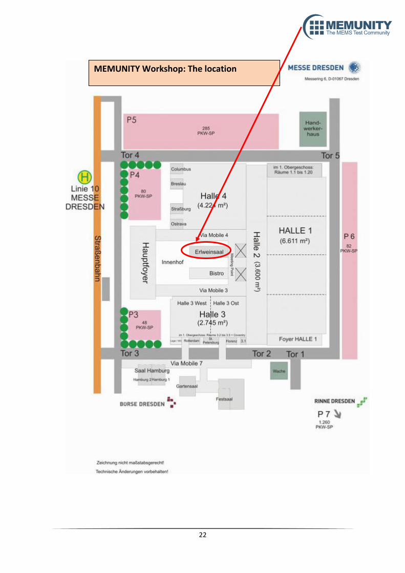
22
MEMUNITY Workshop: The location