Embed Size (px)
Citation preview
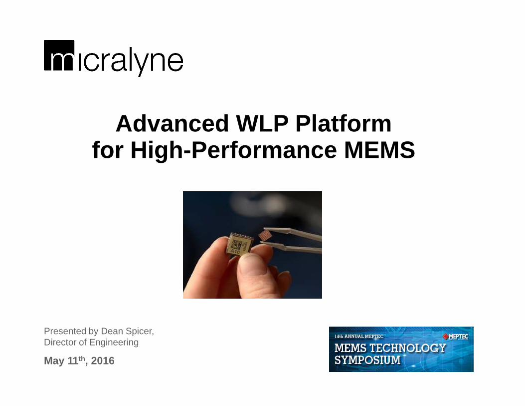
Advanced WLP Platformfor High -Performance MEMS
11
Presented by Dean SpicerDirector of Engineering
May 11th 2016
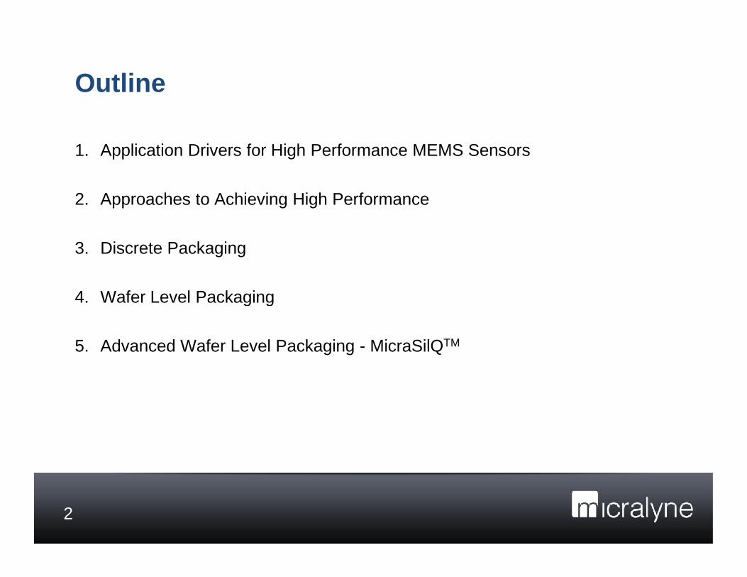
1 Application Drivers for High Performance MEMS Sensors
2 Approaches to Achieving High Performance
3 Discrete Packaging
4 Wafer Level Packaging
Outline
2
4 Wafer Level Packaging
5 Advanced Wafer Level Packaging - MicraSilQTM
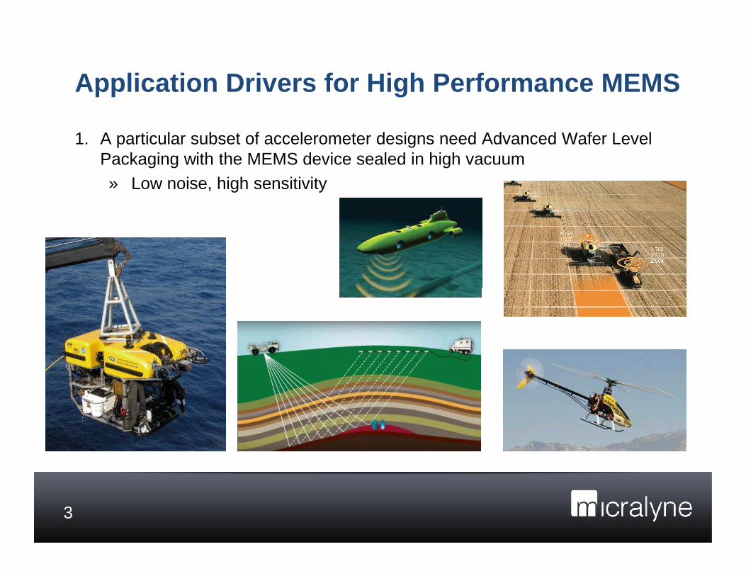
1 A particular subset of accelerometer designs need Advanced Wafer Level Packaging with the MEMS device sealed in high vacuumraquo Low noise high sensitivity
Application Drivers for High Performance MEMS
3
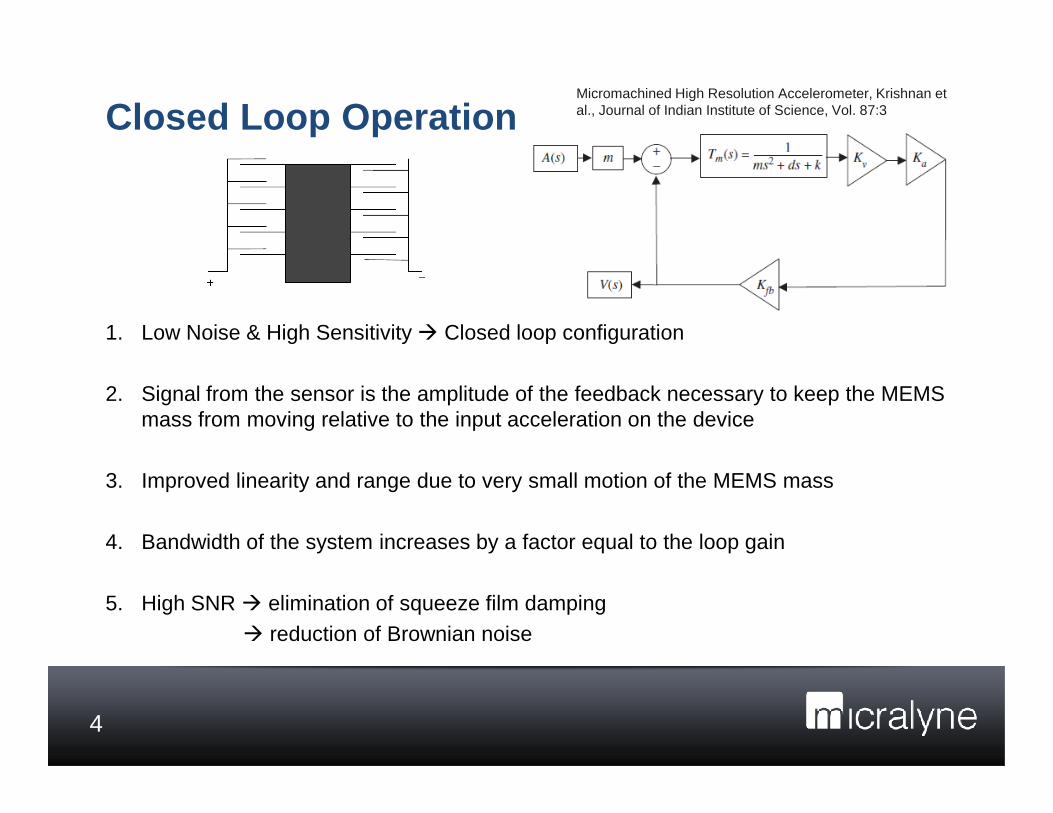
1 Low Noise amp High Sensitivity Closed loop configuration
2 Signal from the sensor is the amplitude of the feedback necessary to keep the MEMS
Closed Loop OperationMicromachined High Resolution Accelerometer Krishnan et al Journal of Indian Institute of Science Vol 873
4
mass from moving relative to the input acceleration on the device
3 Improved linearity and range due to very small motion of the MEMS mass
4 Bandwidth of the system increases by a factor equal to the loop gain
5 High SNR elimination of squeeze film damping reduction of Brownian noise
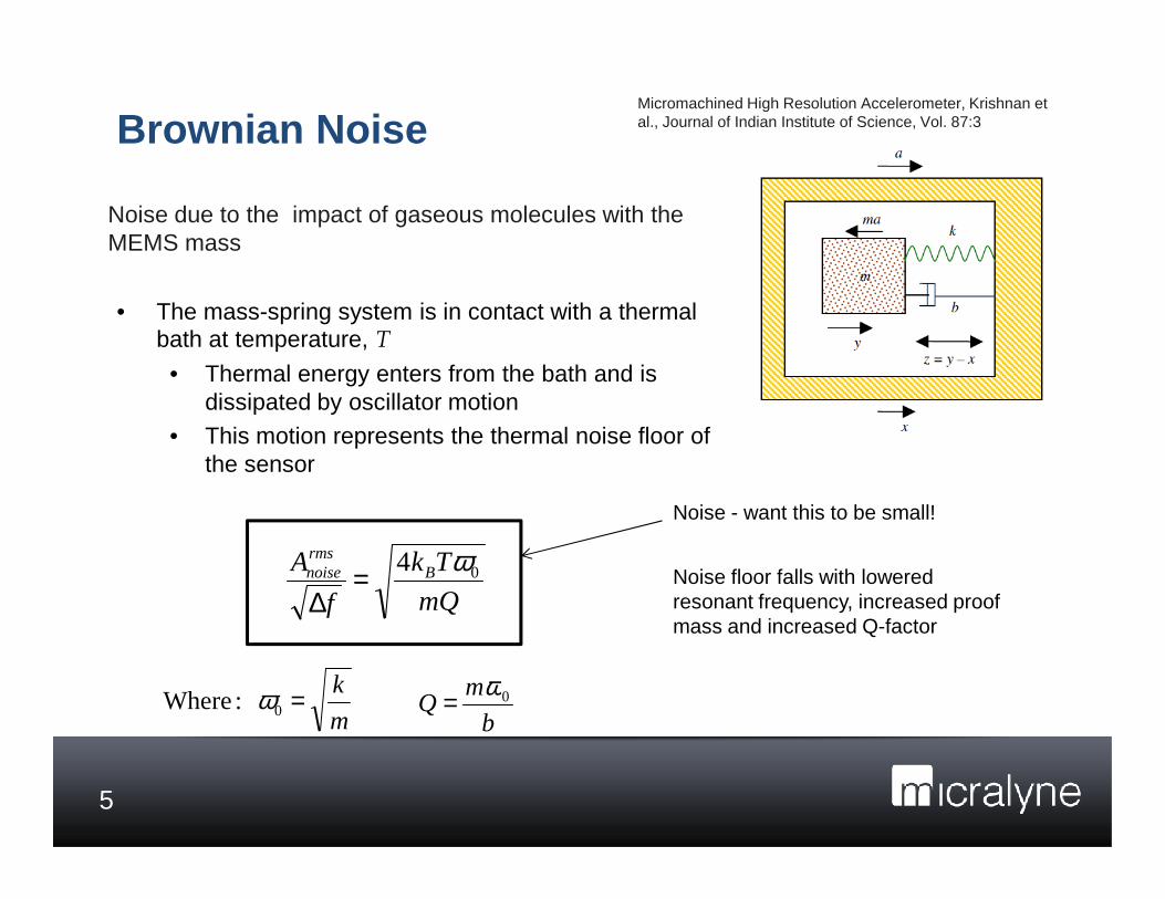
Brownian Noise
bull The mass-spring system is in contact with a thermal bath at temperature T
bull Thermal energy enters from the bath and is dissipated by oscillator motion
bull This motion represents the thermal noise floor of
T
Noise due to the impact of gaseous molecules with the MEMS mass
Micromachined High Resolution Accelerometer Krishnan et al Journal of Indian Institute of Science Vol 873
5
the sensor
mQ
Tk
f
A Brmsnoise 04 ω=∆
Noise floor falls with lowered resonant frequency increased proof mass and increased Q-factor
Noise - want this to be small
m
k=0 Where ωb
mQ 0ω=
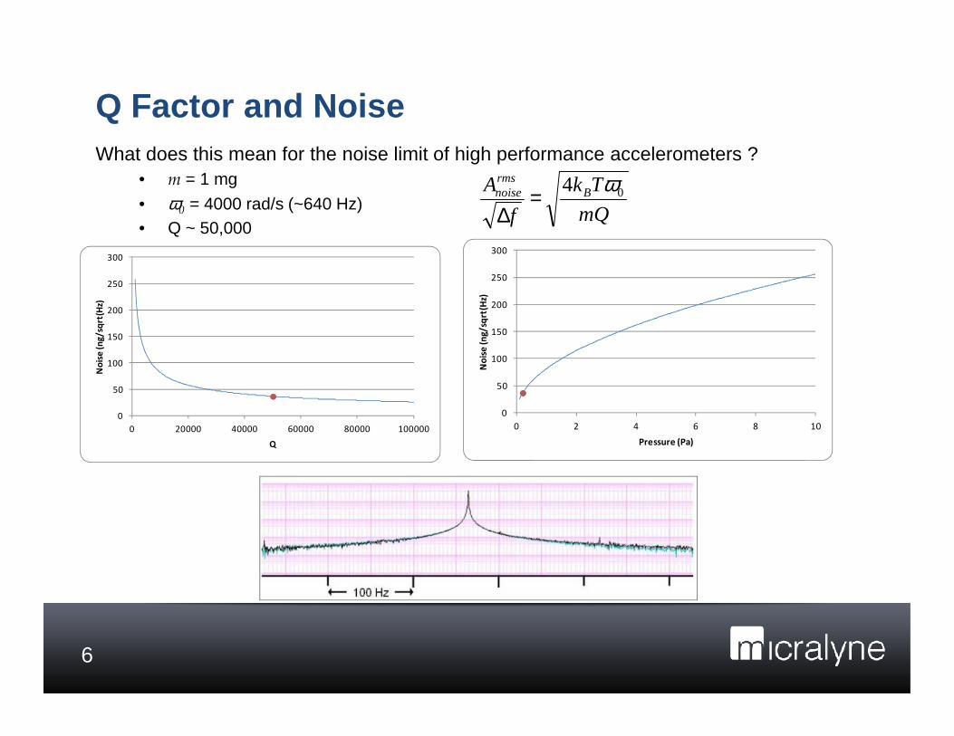
Q Factor and NoiseWhat does this mean for the noise limit of high performance accelerometers
bull m = 1 mg
bull ω0
= 4000 rads (~640 Hz)bull Q ~ 50000
mQ
Tk
f
A Brmsnoise 04 ω=∆
100
150
200
250
300
No
ise
(n
g
sqrt
(Hz)
100
150
200
250
300
No
ise
(n
g
sqrt
(Hz)
6
0
50
100
0 20000 40000 60000 80000 100000
No
ise
(n
g
sqrt
(Hz)
Q
0
50
0 2 4 6 8 10
No
ise
(n
g
sqrt
(Hz)
Pressure (Pa)
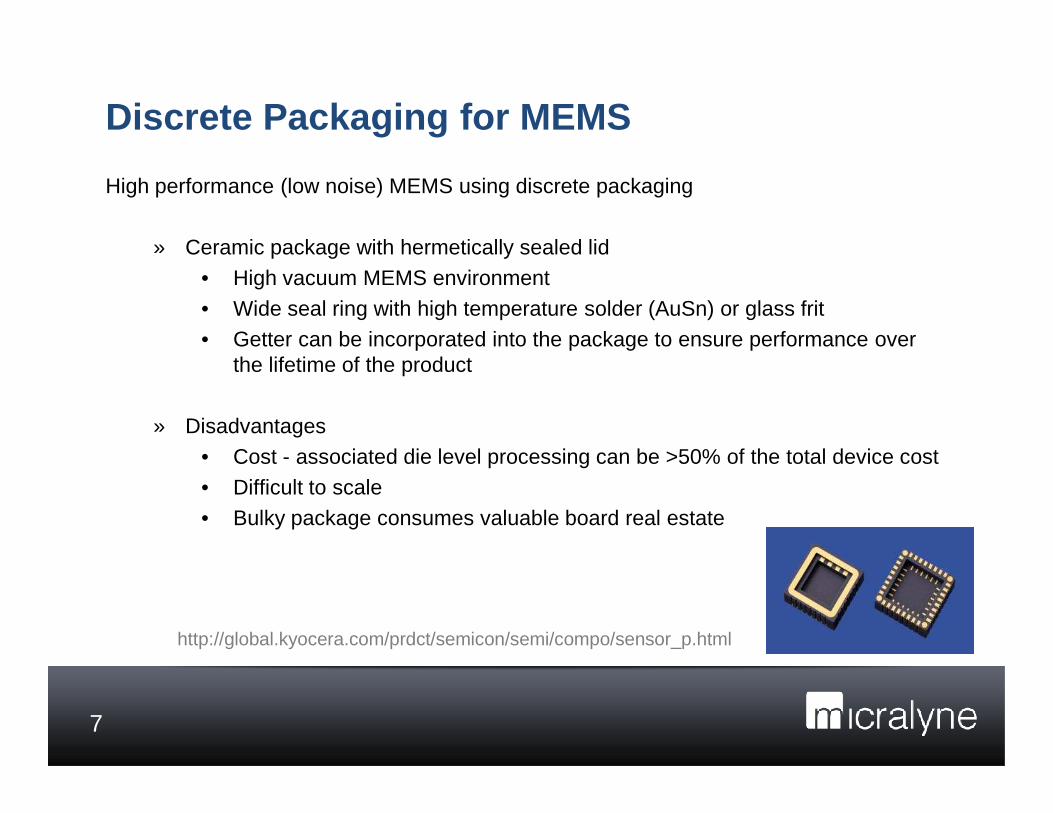
High performance (low noise) MEMS using discrete packaging
raquo Ceramic package with hermetically sealed lidbull High vacuum MEMS environmentbull Wide seal ring with high temperature solder (AuSn) or glass fritbull Getter can be incorporated into the package to ensure performance over
the lifetime of the product
Discrete Packaging for MEMS
7
raquo Disadvantagesbull Cost - associated die level processing can be gt50 of the total device costbull Difficult to scalebull Bulky package consumes valuable board real estate
httpglobalkyoceracomprdctsemiconsemicomposensor_phtml
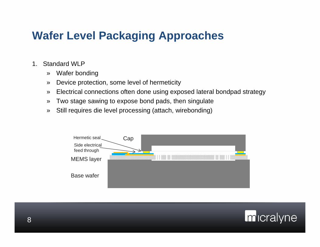
1 Standard WLPraquo Wafer bondingraquo Device protection some level of hermeticityraquo Electrical connections often done using exposed lateral bondpad strategyraquo Two stage sawing to expose bond pads then singulateraquo Still requires die level processing (attach wirebonding)
Wafer Level Packaging Approaches
8
Cap
MEMS layer
Side electrical feed through
Base wafer
Hermetic seal
Lid Wafer
Device Wafer
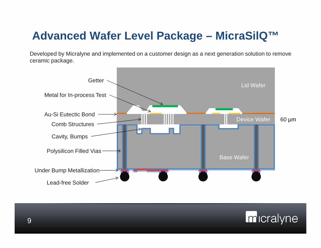
Getter
Metal for In-process Test
Au-Si Eutectic Bond
Comb Structures
Advanced Wafer Level Package ndash MicraSilQ trade
60 microm
Developed by Micralyne and implemented on a customer design as a next generation solution to remove ceramic package
9
Base Wafer
Comb Structures
Cavity Bumps
Polysilicon Filled Vias
Under Bump Metallization
Lead-free Solder
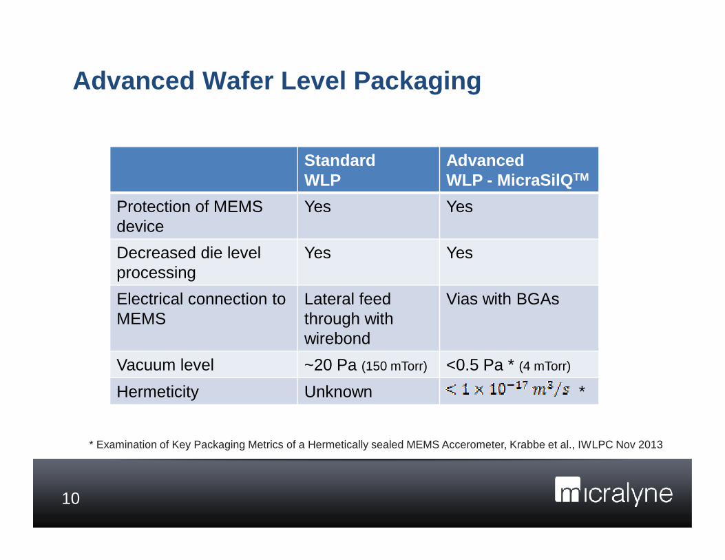
Advanced Wafer Level Packaging
StandardWLP
AdvancedWLP - MicraSilQ TM
Protection of MEMS device
Yes Yes
Decreased die level processing
Yes Yes
10
processing
Electrical connection to MEMS
Lateral feed through with wirebond
Vias with BGAs
Vacuum level ~20 Pa (150 mTorr) lt05 Pa (4 mTorr)
Hermeticity Unknown
Examination of Key Packaging Metrics of a Hermetically sealed MEMS Accerometer Krabbe et al IWLPC Nov 2013
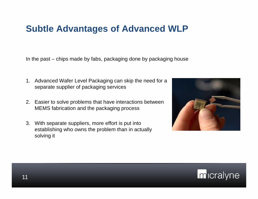
In the past ndash chips made by fabs packaging done by packaging house
Subtle Advantages of Advanced WLP
1 Advanced Wafer Level Packaging can skip the need for a separate supplier of packaging services
2 Easier to solve problems that have interactions between
11
2 Easier to solve problems that have interactions between MEMS fabrication and the packaging process
3 With separate suppliers more effort is put into establishing who owns the problem than in actually solving it
bull Hermeticity of the bonding technologies is key to fabricating a MEMS inertial sensor capable of high Q factors
bull Bottom wafers are fusion bonded
bullTop wafer is bonded by the formation of Gold-Silicon Eutectic above 363ordmC
Three Functional Silicon Layers ndash Two Bonds
DSID-0C0903A9
12
bull Exact bond parameters are critical to the success of the bond and the ultimate performance of the device
bull vacuum levelbull temperature profile
bull Typical bond line is ~100 microm (compare to 500 microm ndash 1500 microm for solder seal of ceramic package)
DSID-0C0903A9
Lid
Device
Base400 microm
60 microm
500 microm
ldquoVia Firstrdquo process
Through Silicon Via Details
13
Key TSV characteristicsraquo Doped poly-Si fill materialraquo 400 micromraquo gt100 MΩ isolation from the substrateraquo lt5 pF parasitic capacitance raquo TSV resistivity lt 4 mΩcmraquo lt 10Ω via resistance UBM and BGA
Lid
Device
Base
Integrated Getter Cavity Design
DSID-0C0903A9
Lid Wafer
Device Wafer 60 microm
500 microm
10 microm gap
50 microm gap
Patternable Getter (2um)
14
Base Wafer
400 microm
20 microm gap
bull Getter is deposited on the lid wafer prior to bonding
bull Cavity around the MEMS can be designed with bump stops
bull AlSi metallization for backside metal traces (allows for re-distribution of the contacts)bull Passivation layer for damage protection and electrical isolation
bull Under bump metallization (UBM) suitable for lead free solder ballsbull SAC 405 solder balls (035 mm diameter)bull Solder balls are placed and then reflowedbull Ball attached yield of 999 across wafer
Backside Metallization and UBM
15
bull Ball attached yield of 999 across wafer
bull Singulated chip is ready for direct attachment to boardbull UBM optimized to ensure reliable attachment to FR4
MicraSilQ trade
Wafer Level Packaging Platform
bull gt 50 Reduced cost through elimination of external packaging
bull Established process for fast ramp to manufacturing Accelerometer Gyroscope
16
bull Simple board reflow mounting
bull Custom device layer for your unique application
Design Kit Available
Through Silicon Via
(TSV)
Lead free solder
1 Thinner dieraquo Thinning of lid wafer straight forwardraquo Thinning of base wafer requires development
2 Thicker Device Layer raquo Allows increased mass of the MEMS
(therefore lower noise floor)
Next Steps for MicraSilQ TM
Lid
Device
400 microm
60 microm
500 microm
17
3 Vias with metal fillraquo Requires developmentraquo Via material would have to survive the
eutectic bond process
Base400 microm
Micralyne Consolidated Overviewbull Founded 1982 (privatized 1998)bull Headquartered in Edmonton
Alberta CAbull Facilities 55000 Sq Ft (5000m2)
bull MEMS Fab Test Metrology Packaging Administration
bull 6rdquo (150mm) Wafer Productionbull Capacity variable based on mix
bull 5K ndash 10K wafers per month based on 5 layer process
bull ISO 9001 and ISO 13485 certified
bull Core Capabilitiesbull MEMS and Micro-fabrication on
Silicon Glass Quartz and other base wafer materials
bull MEMS Process and Micro Structure IP bull More than 30 years of micro and nano
manufacturing ldquoknow howrdquo
bull Focus Marketsbull Industrial Sensorsbull Bio and Medical Sensors
18
bull ISO 9001 and ISO 13485 certifiedbull 83 Employeesbull Customers
bull Fortune 500 System OEMs bull Fabless MEMS Product Companiesbull Medical Optical and Industrial Device
Companies
bull Bio and Medical Sensorsbull Optical Communications
bull Engagement Modelbull Engineering Services
bull Process Design and Process Integrationbull Modeling and Analysis
bull Manufacturing Servicesbull Proof of Concept and Prototypebull Volume Wafer Productionbull Backend Packaging and Test
18
Thank You
19
Dean Spicer Director of Engineeringdeansmicralynecom
Tel 780 431 4411 x2256
Paul PickeringVP Sales amp Marketingpaulpmicralynecom
Tel 408 981 5830
1 Application Drivers for High Performance MEMS Sensors
2 Approaches to Achieving High Performance
3 Discrete Packaging
4 Wafer Level Packaging
Outline
2
4 Wafer Level Packaging
5 Advanced Wafer Level Packaging - MicraSilQTM
1 A particular subset of accelerometer designs need Advanced Wafer Level Packaging with the MEMS device sealed in high vacuumraquo Low noise high sensitivity
Application Drivers for High Performance MEMS
3
1 Low Noise amp High Sensitivity Closed loop configuration
2 Signal from the sensor is the amplitude of the feedback necessary to keep the MEMS
Closed Loop OperationMicromachined High Resolution Accelerometer Krishnan et al Journal of Indian Institute of Science Vol 873
4
mass from moving relative to the input acceleration on the device
3 Improved linearity and range due to very small motion of the MEMS mass
4 Bandwidth of the system increases by a factor equal to the loop gain
5 High SNR elimination of squeeze film damping reduction of Brownian noise
Brownian Noise
bull The mass-spring system is in contact with a thermal bath at temperature T
bull Thermal energy enters from the bath and is dissipated by oscillator motion
bull This motion represents the thermal noise floor of
T
Noise due to the impact of gaseous molecules with the MEMS mass
Micromachined High Resolution Accelerometer Krishnan et al Journal of Indian Institute of Science Vol 873
5
the sensor
mQ
Tk
f
A Brmsnoise 04 ω=∆
Noise floor falls with lowered resonant frequency increased proof mass and increased Q-factor
Noise - want this to be small
m
k=0 Where ωb
mQ 0ω=
Q Factor and NoiseWhat does this mean for the noise limit of high performance accelerometers
bull m = 1 mg
bull ω0
= 4000 rads (~640 Hz)bull Q ~ 50000
mQ
Tk
f
A Brmsnoise 04 ω=∆
100
150
200
250
300
No
ise
(n
g
sqrt
(Hz)
100
150
200
250
300
No
ise
(n
g
sqrt
(Hz)
6
0
50
100
0 20000 40000 60000 80000 100000
No
ise
(n
g
sqrt
(Hz)
Q
0
50
0 2 4 6 8 10
No
ise
(n
g
sqrt
(Hz)
Pressure (Pa)
High performance (low noise) MEMS using discrete packaging
raquo Ceramic package with hermetically sealed lidbull High vacuum MEMS environmentbull Wide seal ring with high temperature solder (AuSn) or glass fritbull Getter can be incorporated into the package to ensure performance over
the lifetime of the product
Discrete Packaging for MEMS
7
raquo Disadvantagesbull Cost - associated die level processing can be gt50 of the total device costbull Difficult to scalebull Bulky package consumes valuable board real estate
httpglobalkyoceracomprdctsemiconsemicomposensor_phtml
1 Standard WLPraquo Wafer bondingraquo Device protection some level of hermeticityraquo Electrical connections often done using exposed lateral bondpad strategyraquo Two stage sawing to expose bond pads then singulateraquo Still requires die level processing (attach wirebonding)
Wafer Level Packaging Approaches
8
Cap
MEMS layer
Side electrical feed through
Base wafer
Hermetic seal
Lid Wafer
Device Wafer
Getter
Metal for In-process Test
Au-Si Eutectic Bond
Comb Structures
Advanced Wafer Level Package ndash MicraSilQ trade
60 microm
Developed by Micralyne and implemented on a customer design as a next generation solution to remove ceramic package
9
Base Wafer
Comb Structures
Cavity Bumps
Polysilicon Filled Vias
Under Bump Metallization
Lead-free Solder
Advanced Wafer Level Packaging
StandardWLP
AdvancedWLP - MicraSilQ TM
Protection of MEMS device
Yes Yes
Decreased die level processing
Yes Yes
10
processing
Electrical connection to MEMS
Lateral feed through with wirebond
Vias with BGAs
Vacuum level ~20 Pa (150 mTorr) lt05 Pa (4 mTorr)
Hermeticity Unknown
Examination of Key Packaging Metrics of a Hermetically sealed MEMS Accerometer Krabbe et al IWLPC Nov 2013
In the past ndash chips made by fabs packaging done by packaging house
Subtle Advantages of Advanced WLP
1 Advanced Wafer Level Packaging can skip the need for a separate supplier of packaging services
2 Easier to solve problems that have interactions between
11
2 Easier to solve problems that have interactions between MEMS fabrication and the packaging process
3 With separate suppliers more effort is put into establishing who owns the problem than in actually solving it
bull Hermeticity of the bonding technologies is key to fabricating a MEMS inertial sensor capable of high Q factors
bull Bottom wafers are fusion bonded
bullTop wafer is bonded by the formation of Gold-Silicon Eutectic above 363ordmC
Three Functional Silicon Layers ndash Two Bonds
DSID-0C0903A9
12
bull Exact bond parameters are critical to the success of the bond and the ultimate performance of the device
bull vacuum levelbull temperature profile
bull Typical bond line is ~100 microm (compare to 500 microm ndash 1500 microm for solder seal of ceramic package)
DSID-0C0903A9
Lid
Device
Base400 microm
60 microm
500 microm
ldquoVia Firstrdquo process
Through Silicon Via Details
13
Key TSV characteristicsraquo Doped poly-Si fill materialraquo 400 micromraquo gt100 MΩ isolation from the substrateraquo lt5 pF parasitic capacitance raquo TSV resistivity lt 4 mΩcmraquo lt 10Ω via resistance UBM and BGA
Lid
Device
Base
Integrated Getter Cavity Design
DSID-0C0903A9
Lid Wafer
Device Wafer 60 microm
500 microm
10 microm gap
50 microm gap
Patternable Getter (2um)
14
Base Wafer
400 microm
20 microm gap
bull Getter is deposited on the lid wafer prior to bonding
bull Cavity around the MEMS can be designed with bump stops
bull AlSi metallization for backside metal traces (allows for re-distribution of the contacts)bull Passivation layer for damage protection and electrical isolation
bull Under bump metallization (UBM) suitable for lead free solder ballsbull SAC 405 solder balls (035 mm diameter)bull Solder balls are placed and then reflowedbull Ball attached yield of 999 across wafer
Backside Metallization and UBM
15
bull Ball attached yield of 999 across wafer
bull Singulated chip is ready for direct attachment to boardbull UBM optimized to ensure reliable attachment to FR4
MicraSilQ trade
Wafer Level Packaging Platform
bull gt 50 Reduced cost through elimination of external packaging
bull Established process for fast ramp to manufacturing Accelerometer Gyroscope
16
bull Simple board reflow mounting
bull Custom device layer for your unique application
Design Kit Available
Through Silicon Via
(TSV)
Lead free solder
1 Thinner dieraquo Thinning of lid wafer straight forwardraquo Thinning of base wafer requires development
2 Thicker Device Layer raquo Allows increased mass of the MEMS
(therefore lower noise floor)
Next Steps for MicraSilQ TM
Lid
Device
400 microm
60 microm
500 microm
17
3 Vias with metal fillraquo Requires developmentraquo Via material would have to survive the
eutectic bond process
Base400 microm
Micralyne Consolidated Overviewbull Founded 1982 (privatized 1998)bull Headquartered in Edmonton
Alberta CAbull Facilities 55000 Sq Ft (5000m2)
bull MEMS Fab Test Metrology Packaging Administration
bull 6rdquo (150mm) Wafer Productionbull Capacity variable based on mix
bull 5K ndash 10K wafers per month based on 5 layer process
bull ISO 9001 and ISO 13485 certified
bull Core Capabilitiesbull MEMS and Micro-fabrication on
Silicon Glass Quartz and other base wafer materials
bull MEMS Process and Micro Structure IP bull More than 30 years of micro and nano
manufacturing ldquoknow howrdquo
bull Focus Marketsbull Industrial Sensorsbull Bio and Medical Sensors
18
bull ISO 9001 and ISO 13485 certifiedbull 83 Employeesbull Customers
bull Fortune 500 System OEMs bull Fabless MEMS Product Companiesbull Medical Optical and Industrial Device
Companies
bull Bio and Medical Sensorsbull Optical Communications
bull Engagement Modelbull Engineering Services
bull Process Design and Process Integrationbull Modeling and Analysis
bull Manufacturing Servicesbull Proof of Concept and Prototypebull Volume Wafer Productionbull Backend Packaging and Test
18
Thank You
19
Dean Spicer Director of Engineeringdeansmicralynecom
Tel 780 431 4411 x2256
Paul PickeringVP Sales amp Marketingpaulpmicralynecom
Tel 408 981 5830
Lid Wafer
Device Wafer
Getter
Metal for In-process Test
Au-Si Eutectic Bond
Comb Structures
Advanced Wafer Level Package ndash MicraSilQ trade
60 microm
Developed by Micralyne and implemented on a customer design as a next generation solution to remove ceramic package
9
Base Wafer
Comb Structures
Cavity Bumps
Polysilicon Filled Vias
Under Bump Metallization
Lead-free Solder
Advanced Wafer Level Packaging
StandardWLP
AdvancedWLP - MicraSilQ TM
Protection of MEMS device
Yes Yes
Decreased die level processing
Yes Yes
10
processing
Electrical connection to MEMS
Lateral feed through with wirebond
Vias with BGAs
Vacuum level ~20 Pa (150 mTorr) lt05 Pa (4 mTorr)
Hermeticity Unknown
Examination of Key Packaging Metrics of a Hermetically sealed MEMS Accerometer Krabbe et al IWLPC Nov 2013
In the past ndash chips made by fabs packaging done by packaging house
Subtle Advantages of Advanced WLP
1 Advanced Wafer Level Packaging can skip the need for a separate supplier of packaging services
2 Easier to solve problems that have interactions between
11
2 Easier to solve problems that have interactions between MEMS fabrication and the packaging process
3 With separate suppliers more effort is put into establishing who owns the problem than in actually solving it
bull Hermeticity of the bonding technologies is key to fabricating a MEMS inertial sensor capable of high Q factors
bull Bottom wafers are fusion bonded
bullTop wafer is bonded by the formation of Gold-Silicon Eutectic above 363ordmC
Three Functional Silicon Layers ndash Two Bonds
DSID-0C0903A9
12
bull Exact bond parameters are critical to the success of the bond and the ultimate performance of the device
bull vacuum levelbull temperature profile
bull Typical bond line is ~100 microm (compare to 500 microm ndash 1500 microm for solder seal of ceramic package)
DSID-0C0903A9
Lid
Device
Base400 microm
60 microm
500 microm
ldquoVia Firstrdquo process
Through Silicon Via Details
13
Key TSV characteristicsraquo Doped poly-Si fill materialraquo 400 micromraquo gt100 MΩ isolation from the substrateraquo lt5 pF parasitic capacitance raquo TSV resistivity lt 4 mΩcmraquo lt 10Ω via resistance UBM and BGA
Lid
Device
Base
Integrated Getter Cavity Design
DSID-0C0903A9
Lid Wafer
Device Wafer 60 microm
500 microm
10 microm gap
50 microm gap
Patternable Getter (2um)
14
Base Wafer
400 microm
20 microm gap
bull Getter is deposited on the lid wafer prior to bonding
bull Cavity around the MEMS can be designed with bump stops
bull AlSi metallization for backside metal traces (allows for re-distribution of the contacts)bull Passivation layer for damage protection and electrical isolation
bull Under bump metallization (UBM) suitable for lead free solder ballsbull SAC 405 solder balls (035 mm diameter)bull Solder balls are placed and then reflowedbull Ball attached yield of 999 across wafer
Backside Metallization and UBM
15
bull Ball attached yield of 999 across wafer
bull Singulated chip is ready for direct attachment to boardbull UBM optimized to ensure reliable attachment to FR4
MicraSilQ trade
Wafer Level Packaging Platform
bull gt 50 Reduced cost through elimination of external packaging
bull Established process for fast ramp to manufacturing Accelerometer Gyroscope
16
bull Simple board reflow mounting
bull Custom device layer for your unique application
Design Kit Available
Through Silicon Via
(TSV)
Lead free solder
1 Thinner dieraquo Thinning of lid wafer straight forwardraquo Thinning of base wafer requires development
2 Thicker Device Layer raquo Allows increased mass of the MEMS
(therefore lower noise floor)
Next Steps for MicraSilQ TM
Lid
Device
400 microm
60 microm
500 microm
17
3 Vias with metal fillraquo Requires developmentraquo Via material would have to survive the
eutectic bond process
Base400 microm
Micralyne Consolidated Overviewbull Founded 1982 (privatized 1998)bull Headquartered in Edmonton
Alberta CAbull Facilities 55000 Sq Ft (5000m2)
bull MEMS Fab Test Metrology Packaging Administration
bull 6rdquo (150mm) Wafer Productionbull Capacity variable based on mix
bull 5K ndash 10K wafers per month based on 5 layer process
bull ISO 9001 and ISO 13485 certified
bull Core Capabilitiesbull MEMS and Micro-fabrication on
Silicon Glass Quartz and other base wafer materials
bull MEMS Process and Micro Structure IP bull More than 30 years of micro and nano
manufacturing ldquoknow howrdquo
bull Focus Marketsbull Industrial Sensorsbull Bio and Medical Sensors
18
bull ISO 9001 and ISO 13485 certifiedbull 83 Employeesbull Customers
bull Fortune 500 System OEMs bull Fabless MEMS Product Companiesbull Medical Optical and Industrial Device
Companies
bull Bio and Medical Sensorsbull Optical Communications
bull Engagement Modelbull Engineering Services
bull Process Design and Process Integrationbull Modeling and Analysis
bull Manufacturing Servicesbull Proof of Concept and Prototypebull Volume Wafer Productionbull Backend Packaging and Test
18
Thank You
19
Dean Spicer Director of Engineeringdeansmicralynecom
Tel 780 431 4411 x2256
Paul PickeringVP Sales amp Marketingpaulpmicralynecom
Tel 408 981 5830
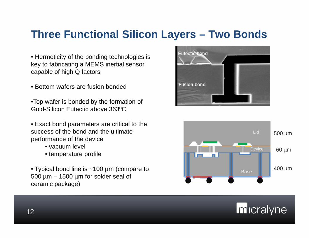
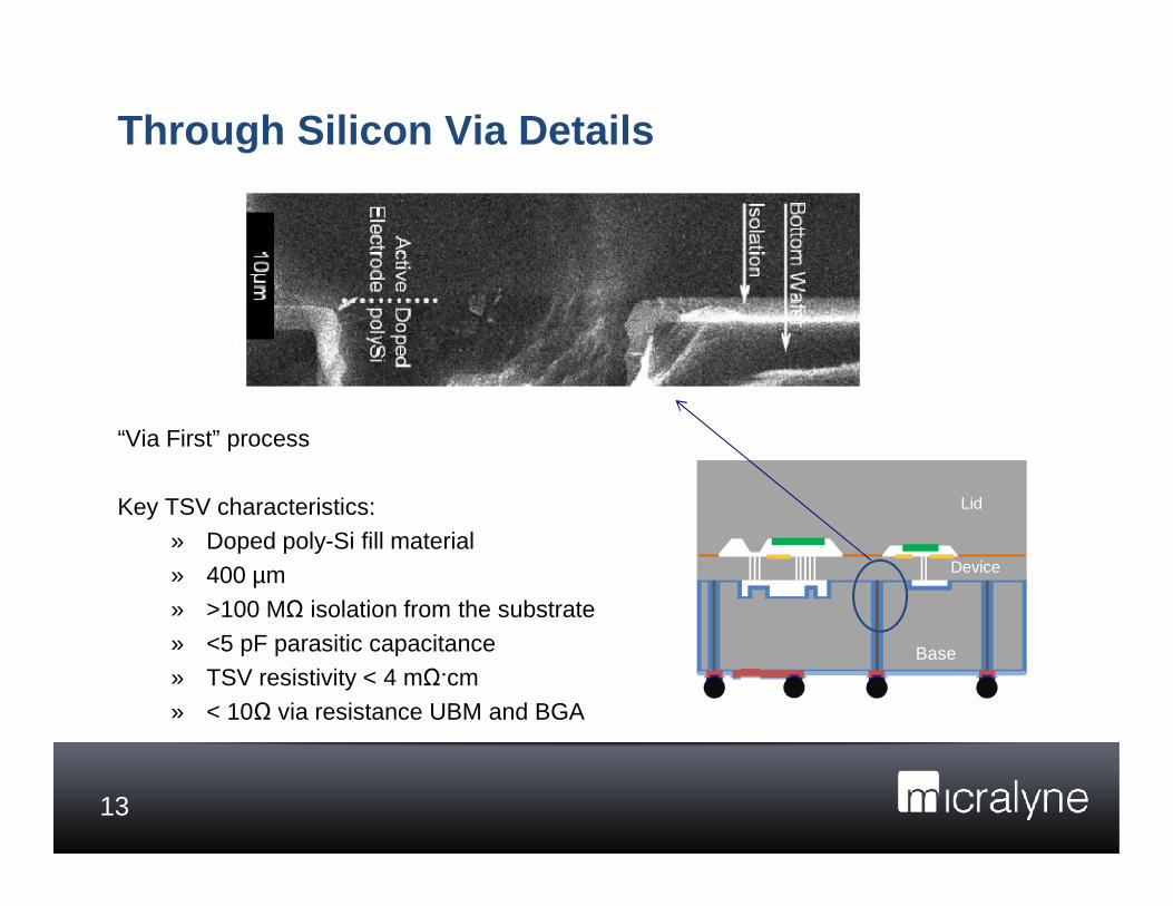
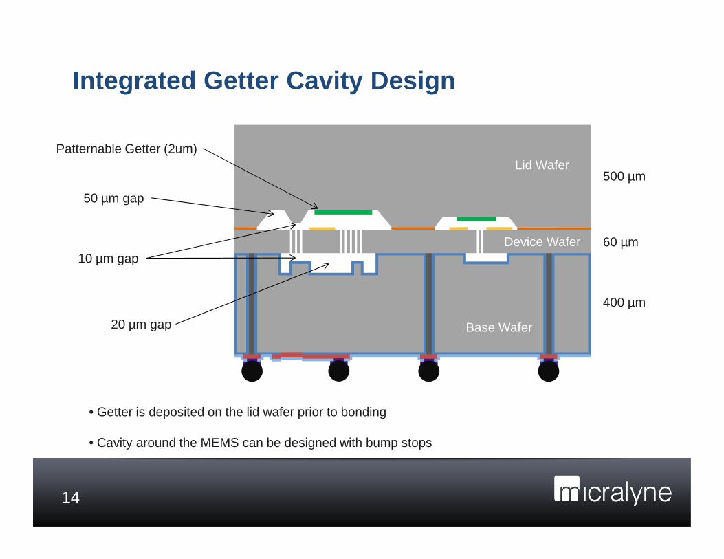
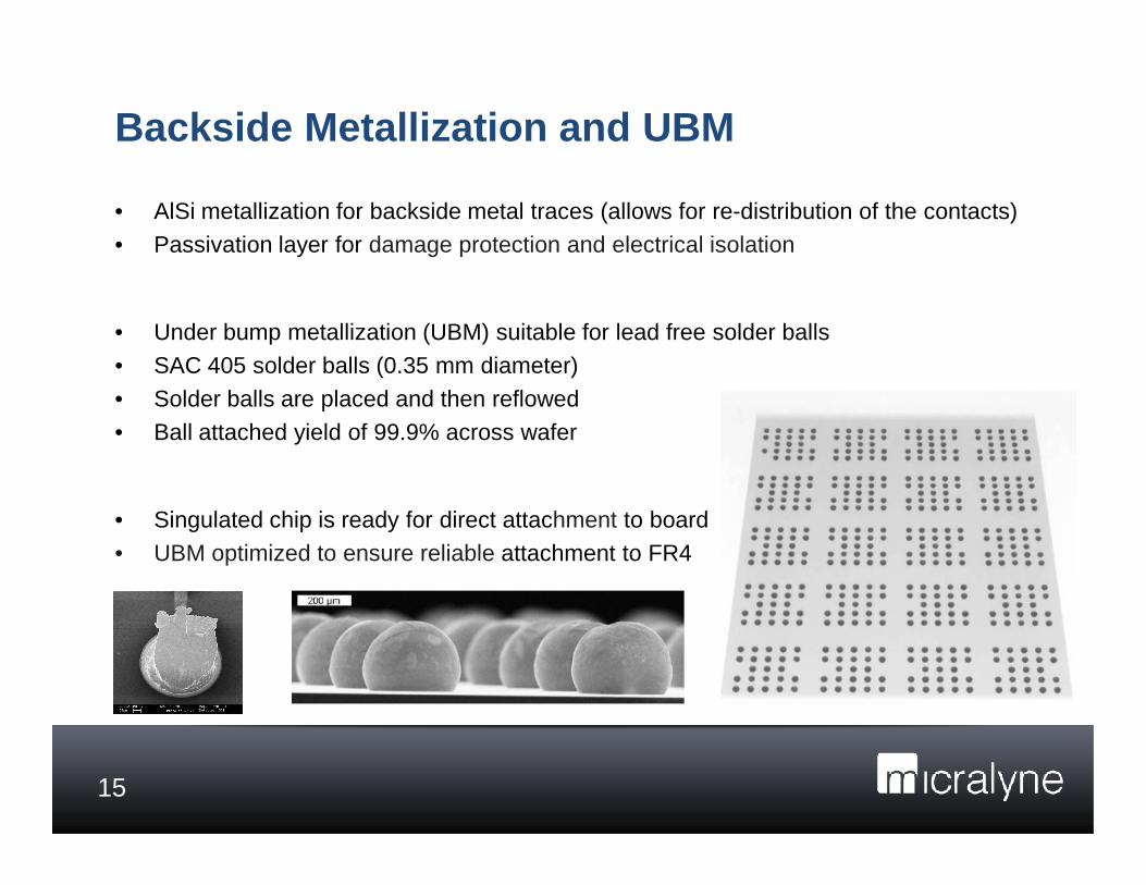
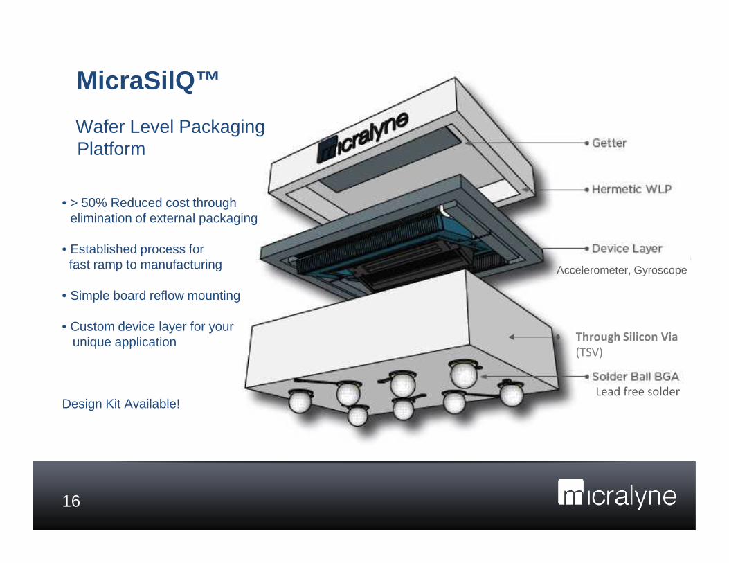
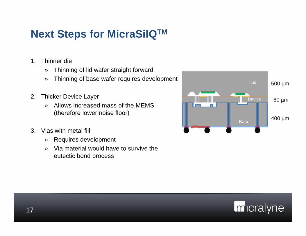
Thank You
19
Dean Spicer Director of Engineeringdeansmicralynecom
Tel 780 431 4411 x2256
Paul PickeringVP Sales amp Marketingpaulpmicralynecom
Tel 408 981 5830