Embed Size (px)
Citation preview

General rights Copyright and moral rights for the publications made accessible in the public portal are retained by the authors and/or other copyright owners and it is a condition of accessing publications that users recognise and abide by the legal requirements associated with these rights.
• Users may download and print one copy of any publication from the public portal for the purpose of private study or research. • You may not further distribute the material or use it for any profit-making activity or commercial gain • You may freely distribute the URL identifying the publication in the public portal
If you believe that this document breaches copyright please contact us providing details, and we will remove access to the work immediately and investigate your claim.
Downloaded from orbit.dtu.dk on: Jul 12, 2018
Mesoscopic current transport in two-dimensional materials with grain boundaries:Four-point probe resistance and Hall effect
Lotz, Mikkel Rønne; Boll, Mads Kjær; Østerberg, Frederik Westergaard; Hansen, Ole; Petersen, DirchHjorthPublished in:Journal of Applied Physics
Link to article, DOI:10.1063/1.4963719
Publication date:2016
Document VersionPublisher's PDF, also known as Version of record
Link back to DTU Orbit
Citation (APA):Lotz, M. R., Boll, M., Østerberg, F. W., Hansen, O., & Petersen, D. H. (2016). Mesoscopic current transport intwo-dimensional materials with grain boundaries: Four-point probe resistance and Hall effect. Journal of AppliedPhysics, 120(13), [134303]. DOI: 10.1063/1.4963719

Mesoscopic current transport in two-dimensional materials with grain boundaries:Four-point probe resistance and Hall effectMikkel R. Lotz, Mads Boll, Frederik W. Østerberg, Ole Hansen, and Dirch H. Petersen Citation: Journal of Applied Physics 120, 134303 (2016); doi: 10.1063/1.4963719 View online: http://dx.doi.org/10.1063/1.4963719 View Table of Contents: http://scitation.aip.org/content/aip/journal/jap/120/13?ver=pdfcov Published by the AIP Publishing Articles you may be interested in Revealing origin of quasi-one dimensional current transport in defect rich two dimensional materials Appl. Phys. Lett. 105, 053115 (2014); 10.1063/1.4892652 Direct detection of grain boundary scattering in damascene Cu wires by nanoscale four-point probe resistancemeasurements Appl. Phys. Lett. 95, 052110 (2009); 10.1063/1.3202418 Micro-four-point probe Hall effect measurement method J. Appl. Phys. 104, 013710 (2008); 10.1063/1.2949401 Anomalous Hall resistivity due to grain boundary in manganite thin films J. Appl. Phys. 93, 8107 (2003); 10.1063/1.1543865 In situ four-point conductivity and Hall effect apparatus for vacuum and controlled atmosphere measurements ofthin film materials Rev. Sci. Instrum. 73, 2325 (2002); 10.1063/1.1475349
Reuse of AIP Publishing content is subject to the terms at: https://publishing.aip.org/authors/rights-and-permissions. Download to IP: 192.38.67.115 On: Thu, 27 Oct 2016
07:27:41

Mesoscopic current transport in two-dimensional materials with grainboundaries: Four-point probe resistance and Hall effect
Mikkel R. Lotz,1 Mads Boll,1,2 Frederik W. Østerberg,1,3 Ole Hansen,1,4
and Dirch H. Petersen1,a)
1Department of Micro- and Nanotechnology, Technical University of Denmark,DTU Nanotech Building 345 East, DK-2800 Kgs. Lyngby, Denmark2Department of Physics, Technical University of Denmark, DTU Physics Building 309,DK-2800 Kgs. Lyngby, Denmark3CAPRES A/S, Scion-DTU, Building 373, DK-2800 Kgs. Lyngby, Denmark4Danish National Research Foundation’s Center for Individual Nanoparticle Functionality (CINF),Technical University of Denmark, DK-2800 Kgs. Lyngby, Denmark
(Received 28 April 2016; accepted 15 September 2016; published online 3 October 2016)
We have studied the behavior of micro four-point probe (M4PP) measurements on two-dimensional
(2D) sheets composed of grains of varying size and grain boundary resistivity by Monte Carlo based
finite element (FE) modelling. The 2D sheet of the FE model was constructed using Voronoi tessella-
tion to emulate a polycrystalline sheet, and a square sample was cut from the tessellated surface.
Four-point resistances and Hall effect signals were calculated for a probe placed in the center of the
square sample as a function of grain density n and grain boundary resistivity qGB. We find that
the dual configuration sheet resistance as well as the resistance measured between opposing edges of
the square sample have a simple unique dependency on the dimension-less parameterffiffiffi
np
qGBG0,
where G0 is the sheet conductance of a grain. The value of the ratio RA=RB between resistances mea-
sured in A- and B-configurations depends on the dimensionality of the current transport (i.e., one- or
two-dimensional). At low grain density or low grain boundary resistivity, two-dimensional transport
is observed. In contrast, at moderate grain density and high grain resistivity, one-dimensional trans-
port is seen. Ultimately, this affects how measurements on defective systems should be interpreted in
order to extract relevant sample parameters. The Hall effect response in all M4PP configurations was
only significant for moderate grain densities and fairly large grain boundary resistivity. Published byAIP Publishing. [http://dx.doi.org/10.1063/1.4963719]
I. INTRODUCTION
The seminal work on graphene1 has fueled a strong
interest into synthesis, characterization, and application of
graphene as well as other two-dimensional (2D) materials.
However, commercialization of graphene based applications
decidedly calls for the development of reliable methods of
producing high quality graphene and non-destructive meth-
ods to electrically characterize it.2 Synthesis of graphene
using chemical vapor deposition (CVD) has shown great
promise,3,4 yet still contains a wide range of defects com-
pared to its mechanically exfoliated counterpart. These
defects include vacancies, physi- or chemisorbed adatoms,
lattice imperfections, substitutional atoms, and electron-hole
puddles as well as extended defects which include folds,
cracks, and grain boundaries (GBs). GBs are presently ubiq-
uitous in CVD processed material since the technique relies
on stitching together—initially separate—grains in order to
achieve larger coherent sheets.5 Both theoretical6,7 and
experimental studies8,9 on transport through graphene GBs
found that GBs cause potential barriers for the carrier trans-
port and result in an increase in resistance, which sometimes
is 30 times larger than the bulk graphene resistance at the
center of the grain.10–12 Thus, the GBs are significantly
deteriorating the electrical properties of the films, which in
turn affect the performance of graphene based devices, e.g.,
field-effect transistors.13
Micro four-point probe (M4PP) metrology has previ-
ously been used for non-destructive electrical characteriza-
tion of graphene films.14 M4PP metrology can be used to
measure the sheet resistance (or sheet conductance), and in
addition, the method allows for extraction and evaluation of
geometry related parameters such as the resistance ratio15,16
and the Hall effect signal caused by the Lorentz force.17
In previous work,18 we developed a finite element (FE)
model to investigate how the M4PP signature differs for
measurements on 2D and quasi-1D materials; these signa-
tures had already been observed experimentally.15,16 We suc-
cessfully validated the FE approach by comparing
calculations for a single line defect to the analytical result.19
The model was limited in its scope since only samples with
insulating line defects were studied, which may be a reason-
able representation of 2D materials in which current trans-
port is dominated by transfer defects such as rips and tears.
However, with improvements in fabrication of 2D materials,
today transfer defects can now often be neglected. The FE
model proposed here is well suited for simulating M4PP
measurements on 2D materials fabricated by chemical vapor
deposition in which current transport is dominated by intra-
grain conductance and domain boundary resistance. Thea)Electronic mail: [email protected].
0021-8979/2016/120(13)/134303/6/$30.00 Published by AIP Publishing.120, 134303-1
JOURNAL OF APPLIED PHYSICS 120, 134303 (2016)
Reuse of AIP Publishing content is subject to the terms at: https://publishing.aip.org/authors/rights-and-permissions. Download to IP: 192.38.67.115 On: Thu, 27 Oct 2016
07:27:41
model is also more comprehensive than the previous one, as
it also includes an applied magnetic field such that Hall
effects can also be extracted. The model is coupled with a
Monte Carlo approach so that an unbiased correlation
between surface composition and the parameters extracted
from the M4PP measurement can be studied.
We begin our study by defining the four-point notation
we use and a detailed description of the FE model. Then, we
continue to examine the simulation results by comparing the
effective sheet conductances obtained from M4PP and a
square electrode setup, which are shown to largely agree and
follow a predicted dependency on grain boundary resistivity
and grain density. We proceed to study the distribution of
simulated RA=RB ratio as grain boundary resistivity and grain
density are varied, from where it becomes apparent how
important the relative grain size to probe pitch is in affecting
the dimensionality of the current transport. Finally, we study
the effect of grain boundary resistivity and grain density on
the magnitude and distribution of the Hall signal.
II. FOUR-POINT PROBE DEFINITIONS
A four-point probe has 24 possible electrode configura-
tions, 18 of which can be disregarded as they arrive from triv-
ial interchanging of current direction and/or potential pins.
The three remaining configurations in addition to their conju-
gate configurations (where the current pins and voltage poten-
tial pins are interchanged) make up what is known as the
electrode configurations A, B, and C (A0, B0, and C0 for their
respective conjugate configurations). In the A configuration,
the current is applied between pins no. 1 and 4 (pin labels for
the collinear four-point probe are illustrated in Fig. 1), while
the electrical potential is measured between pins no. 2 and 3
such that the resistance becomes RA ¼ V23=I14. In the B con-
figuration, the current is sourced between pins no. 1 and 3,
while pins no. 2 and 4 measure the electrical potential
(RB ¼ V24=I13), and finally, in the C configuration, pins no. 1
and 2 apply the current while pins no. 3 and 4 measure the
potential (RC ¼ V43=I12). The conjugate configurations are
found by interchanging current-carrying pins with the voltage-
sensing pins.
It is convenient to define the average resistance,�Ri ¼ ðRi þ Ri0 Þ=2, and resistance difference, DRi ¼ Ri � Ri0 ,
and where i 2 A;B;C. The Hall effect signal DRi is propor-
tional to the Hall sheet resistance RH and is affected by the
geometry, i.e., the proximity of boundaries obstructing cur-
rent transport. The average resistance �Ri depends on the
sheet resistance including geometrical magnetoresistance.17
For a sample with a highly non-uniform conductance
and samples that are not simply connected, it is furthermore
convenient to redefine the configuration resistances such that
�R ~A � maxðj �RijÞ ; �R ~C � minðj �RijÞ ; �R ~B � �R ~A � �R ~C :
This definition ensures that a dual configuration van der Pauw
conductance always can be found and it limits the modified
resistance ratio to the closed interval �R ~A=�R ~B 2 ½1; 2�, as
opposed to �RA= �RB 2 ��1;1½. The redefinition of configura-
tions only matters in the event of highly non-uniform samples,
e.g., in the presence of a large number of insulating defects in
proximity of the electrodes. In such cases, either of the resis-
tance ratios �RA= �RB; �RA= �RC or �RB= �RC could become unity.
With the configuration redefinition, �R ~A=�R ~B will itself become
unity in cases where any of the values j �RAj; j �RBj or j �RCjapproaches zero.
The van der Pauw equation for collinear four-point
probes in terms of the redefined configurations becomes20
exp ð2p �R ~A~GsÞ � exp ð2p �R ~B
~GsÞ ¼ 1; (1)
which relates the average measured resistances in the ~A and~B configurations to an apparent sheet conductance ~Gs, which
in case of a perfect sample equals the effective sheet conduc-
tance Gs and also the internal grain sheet conductance G0.
Note that Eq. (1) is not valid in the case where �R ~A=�R ~B ¼ 1
(1D conduction).
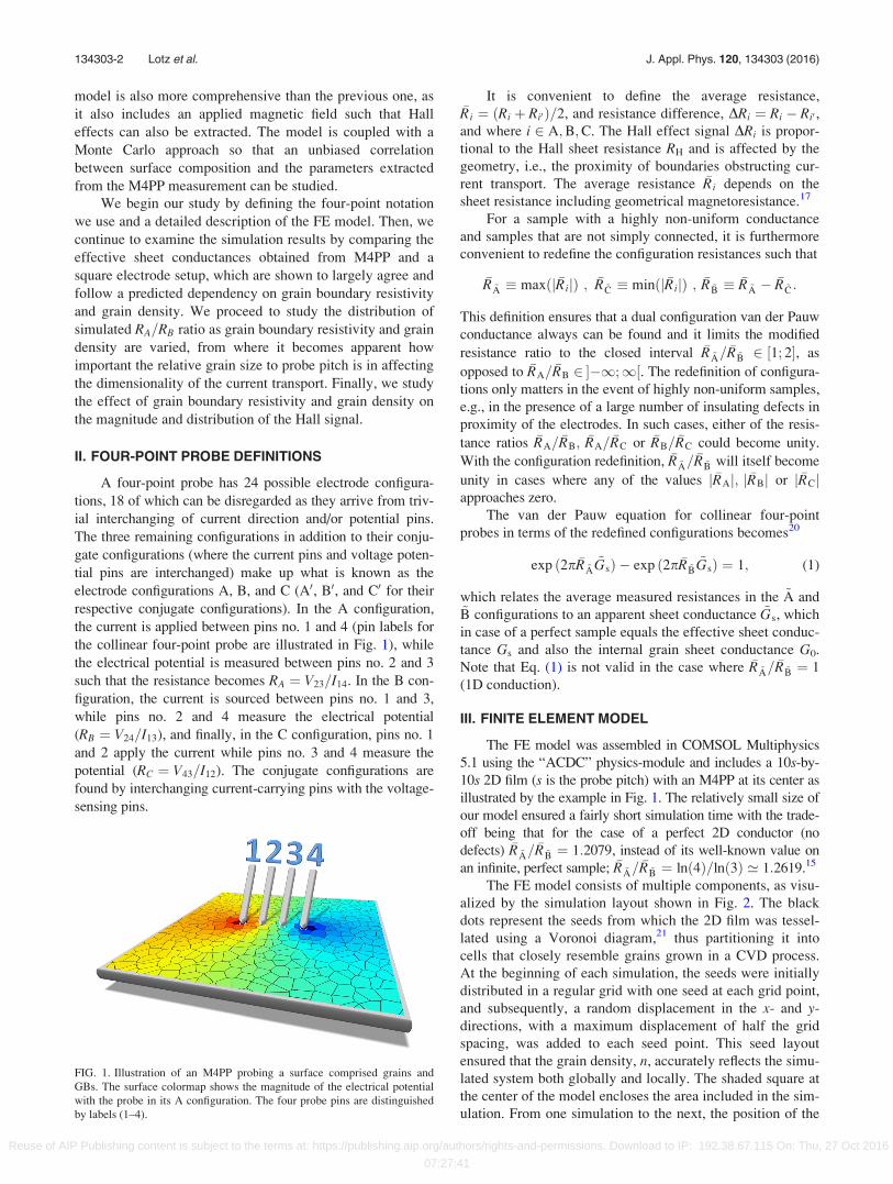
III. FINITE ELEMENT MODEL
The FE model was assembled in COMSOL Multiphysics
5.1 using the “ACDC” physics-module and includes a 10s-by-
10s 2D film (s is the probe pitch) with an M4PP at its center as
illustrated by the example in Fig. 1. The relatively small size of
our model ensured a fairly short simulation time with the trade-
off being that for the case of a perfect 2D conductor (no
defects) �R ~A=�R ~B ¼ 1:2079, instead of its well-known value on
an infinite, perfect sample; �R ~A=�R ~B ¼ lnð4Þ=lnð3Þ ’ 1:2619.15
The FE model consists of multiple components, as visu-
alized by the simulation layout shown in Fig. 2. The black
dots represent the seeds from which the 2D film was tessel-
lated using a Voronoi diagram,21 thus partitioning it into
cells that closely resemble grains grown in a CVD process.
At the beginning of each simulation, the seeds were initially
distributed in a regular grid with one seed at each grid point,
and subsequently, a random displacement in the x- and y-
directions, with a maximum displacement of half the grid
spacing, was added to each seed point. This seed layout
ensured that the grain density, n, accurately reflects the simu-
lated system both globally and locally. The shaded square at
the center of the model encloses the area included in the sim-
ulation. From one simulation to the next, the position of the
FIG. 1. Illustration of an M4PP probing a surface comprised grains and
GBs. The surface colormap shows the magnitude of the electrical potential
with the probe in its A configuration. The four probe pins are distinguished
by labels (1–4).
134303-2 Lotz et al. J. Appl. Phys. 120, 134303 (2016)
Reuse of AIP Publishing content is subject to the terms at: https://publishing.aip.org/authors/rights-and-permissions. Download to IP: 192.38.67.115 On: Thu, 27 Oct 2016
07:27:41
shaded square shifted randomly within the area outlined by the
dashed line. This was done in order to obtain a higher degree
of randomness between each simulated system and to avoid
slight grain density deviations inherent to the Voronoi tessela-
tion when approaching the boundary of the seeded region (out-
lined by the black rim); this was particularly important in low
grain density systems. At the center of the shaded square, four
equally spaced white dots show the positions of the four probe
pins. This symmetric position of the M4PP ensures that in
the case of a perfect uniform film, dual configuration measure-
ments yield the sheet conductance of the material,22 i.e.,~Gs ¼ G0 and that the Hall signals vanish,17 i.e., DRi ¼ 0.
In addition to M4PP measurement calculations, the
model was also adapted to allow calculations of the effective
sheet conductance as illustrated in Fig. 2 (right). The conduc-
tances between iso-potential electrodes on opposing sides of
the square sample, GNS and GEW, were calculated for the
two configurations shown, and the geometric mean reported
as the effective sheet conductance Gs.23,24
Initially, a coarse triangular mesh was applied; then two
adaptive mesh refinement steps followed to optimize the mesh
by increasing the mesh resolution in locations with large
potential gradients, such as close to the current inlets. As
shown in our previous publication,18 two mesh-refinement
steps were sufficient to ensure a relative error of less than 1%
of the fully converged solution. For questions concerning the
validity of this method of modelling M4PP measurements, we
also refer to a previous publication, Ref. 19, where simula-
tions on a simple system containing just a single line defect
were compared to the analytical result.
A. Calculations
For each Voronoi tessellation with a given grain density
n, square samples of 10� 10s2 were cut and M4PP
resistances for all 6 configurations, A, B, C, A0, B0 and C0,calculated for each setting of the grain boundary resistivity.
The sheet resistance of a single grain was kept at R0 ’ 1=G0
¼ 1 X, which defines the resistance scale used. Note, the spe-
cific value of R0 is irrelevant; however, in order to simulate
the problem numerically, we have to assign a value to it.
The grain boundary resistivity, qGB (unit X m), was scaled
in units of R0s, since we have chosen the probe pitch s as the
length scale in our calculations. In the calculations, we have stud-
ied grain boundary resistivities in a range of six orders of magni-
tude, from almost completely transparent (qGBG0s�1 ¼ 10�3) to
almost completely insulating (qGBG0s�1 ¼ 103). By transparent,
we signify that current passes the boundary with an insignificant
potential drop.
Hall effect was included in the calculations by specify-
ing the two-dimensional conductance tensor of the material;
the diagonal elements were set to G0 ¼ 1 S as explained
above, while the off diagonal elements were set to 6GH with
GH ¼ G0lHBz, where lH is the Hall mobility and Bz is the
magnetic flux density normal to the surface. In the calcula-
tions, the product of Hall mobility and magnetic flux density
was fixed at lHBz ¼ 0:01. A relatively small value of lHBz
was chosen to minimize the magnetoresistance effect, which
could complicate interpretation of the results. It follows that
the Hall sheet resistance becomes RH ’ 0:01 X.
IV. RESULTS
A. Effective sheet conductance
The effective sheet conductance Gs is the most impor-
tant parameter in many applications, and it is therefore
important to see how Gs varies with grain density and GB
resistivity; both when Gs is extracted from M4PP measure-
ments and when measured on a square sample with source
and drain electrodes on opposing sides.
Consider a rectangular resistor sample of length L and
width W, which is completely filled with identical square
grains of density n. In this resistor, intra-grain transport con-
tributes R0L=W to the total effective sheet resistance, while the
current has to pass Lffiffiffi
np
grain boundaries of width W, and
therefore, the grain boundaries contribute ðqGB=WÞLffiffiffi
np
to
the total effective sheet resistance, which then becomes
Rs ¼ ðR0 þ qGB
ffiffiffi
npÞL=W, reminiscent of the expression given
in Ref. 9. It follows that the expected effective sheet conduc-
tance normalized to the intra grain sheet conductance becomes
Gs
G0
¼ 1
1þ ffiffiffi
np
qGBG0
; (2)
and thus depends only on a single dimension-less parameterffiffiffi
np
qGBG0. Even though the equation is derived under these
very simplified conditions, we are of the opinion that it has a
more general validity; however, we have not yet found any
analytical proof.
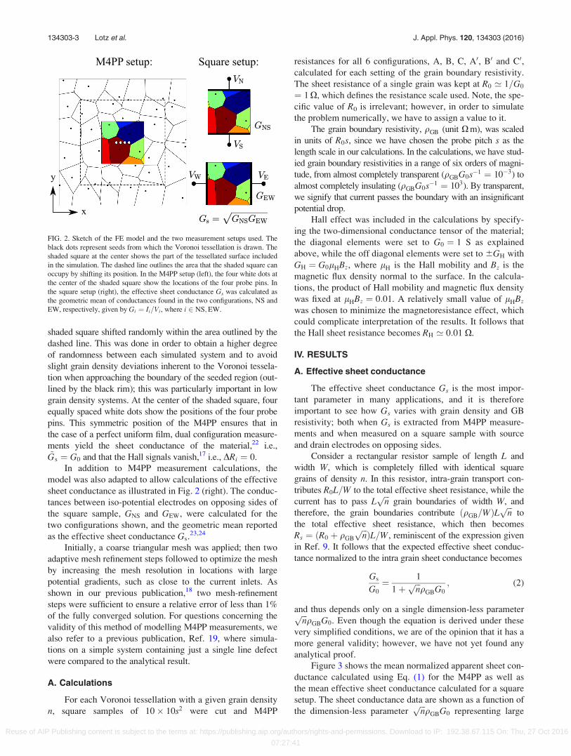
Figure 3 shows the mean normalized apparent sheet con-
ductance calculated using Eq. (1) for the M4PP as well as
the mean effective sheet conductance calculated for a square
setup. The sheet conductance data are shown as a function of
the dimension-less parameterffiffiffi
np
qGBG0 representing large
FIG. 2. Sketch of the FE model and the two measurement setups used. The
black dots represent seeds from which the Voronoi tessellation is drawn. The
shaded square at the center shows the part of the tessellated surface included
in the simulation. The dashed line outlines the area that the shaded square can
occupy by shifting its position. In the M4PP setup (left), the four white dots at
the center of the shaded square show the locations of the four probe pins. In
the square setup (right), the effective sheet conductance Gs was calculated as
the geometric mean of conductances found in the two configurations, NS and
EW, respectively, given by Gi ¼ Ii=Vi, where i 2 NS;EW.
134303-3 Lotz et al. J. Appl. Phys. 120, 134303 (2016)
Reuse of AIP Publishing content is subject to the terms at: https://publishing.aip.org/authors/rights-and-permissions. Download to IP: 192.38.67.115 On: Thu, 27 Oct 2016
07:27:41
variations in both grain density n and GB resistivity qGB. We
see that the majority of the mean sheet conductance data fol-
lows a single unique curve in perfect agreement with Eq. (2).
For low grain density systems, n ¼ ½0:01s�2; 0:25s�2�, the
four-point measurements are expected to deviate from the
analytical model, Eq. (2), as the M4PP is likely to measure
either within a single grain or across a single grain boundary
giving rise to extreme values.
In the square setup, this is less likely to occur since the
distance between electrodes is much larger (10� 10s2); this
explains why a similar deviation is not observed for the
square setup, i.e., the measured conductance is averaged
over a larger number of GBs and is given as the geometric
mean of NS and EW configurations as illustrated in Fig. 2.
The fact that data points from the square setup and M4PP
data points are almost identical show that the M4PP on aver-
age actually measures the effective sheet conductance even
on samples with a high grain boundary density.
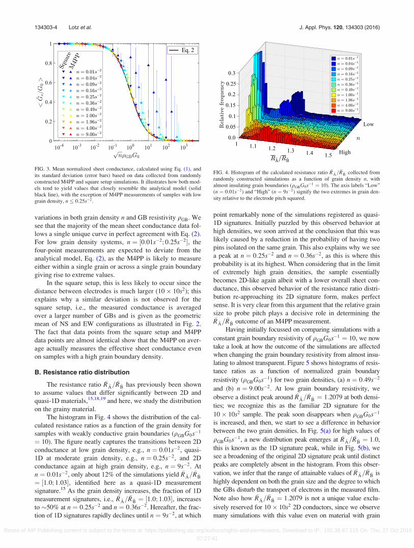
B. Resistance ratio distribution
The resistance ratio �R ~A=�R ~B has previously been shown
to assume values that differ significantly between 2D and
quasi-1D materials,15,18,19 and here, we study the distribution
on the grainy material.
The histogram in Fig. 4 shows the distribution of the cal-
culated resistance ratios as a function of the grain density for
samples with weakly conductive grain boundaries (qGBG0s�1
¼ 10). The figure neatly captures the transitions between 2D
conductance at low grain density, e.g., n ¼ 0:01s�2, quasi-
1D at moderate grain density, e.g., n ¼ 0:25s�2, and 2D
conductance again at high grain density, e.g., n ¼ 9s�2. At
n ¼ 0:01s�2, only about 12% of the simulations yield �R ~A=�R ~B
¼ ½1:0; 1:03�, identified here as a quasi-1D measurement
signature.15 As the grain density increases, the fraction of 1D
measurement signatures, i.e., �R ~A=�R ~B ¼ ½1:0; 1:03�, increases
to �50% at n ¼ 0:25s�2 and n ¼ 0:36s�2. Hereafter, the frac-
tion of 1D signatures rapidly declines until n ¼ 9s�2, at which
point remarkably none of the simulations registered as quasi-
1D signatures. Initially puzzled by this observed behavior at
high densities, we soon arrived at the conclusion that this was
likely caused by a reduction in the probability of having two
pins isolated on the same grain. This also explains why we see
a peak at n ¼ 0:25s�2 and n ¼ 0:36s�2, as this is where this
probability is at its highest. When considering that in the limit
of extremely high grain densities, the sample essentially
becomes 2D-like again albeit with a lower overall sheet con-
ductance, this observed behavior of the resistance ratio distri-
bution re-approaching its 2D signature form, makes perfect
sense. It is very clear from this argument that the relative grain
size to probe pitch plays a decisive role in determining the�R ~A=
�R ~B outcome of an M4PP measurement.
Having initially focussed on comparing simulations with a
constant grain boundary resistivity of qGBG0s�1 ¼ 10, we now
take a look at how the outcome of the simulations are affected
when changing the grain boundary resistivity from almost insu-
lating to almost transparent. Figure 5 shows histograms of resis-
tance ratios as a function of normalized grain boundary
resistivity (qGBG0s�1) for two grain densities, (a) n ¼ 0:49s�2
and (b) n ¼ 9:00s�2. At low grain boundary resistivity, we
observe a distinct peak around �R ~A=�R ~B ¼ 1:2079 at both densi-
ties; we recognize this as the familiar 2D signature for the
10� 10s2 sample. The peak soon disappears when qGBG0s�1
is increased, and then, we start to see a difference in behavior
between the two grain densities. In Fig. 5(a) for high values of
qGBG0s�1, a new distribution peak emerges at �R ~A=�R ~B ¼ 1:0,
this is known as the 1D signature peak, while in Fig. 5(b), we
see a broadening of the original 2D signature peak until distinct
peaks are completely absent in the histogram. From this obser-
vation, we infer that the range of attainable values of �R ~A=�R ~B is
highly dependent on both the grain size and the degree to which
the GBs disturb the transport of electrons in the measured film.
Note also how �R ~A=�R ~B ¼ 1:2079 is not a unique value exclu-
sively reserved for 10� 10s2 2D conductors, since we observe
many simulations with this value even on material with grain
FIG. 3. Mean normalized sheet conductance, calculated using Eq. (1), and
its standard deviation (error bars) based on data collected from randomly
constructed M4PP and square setup simulations. It illustrates how both mod-
els tend to yield values that closely resemble the analytical model (solid
black line), with the exception of M4PP measurements of samples with low
grain density, n � 0:25s�2.
FIG. 4. Histogram of the calculated resistance ratio �R ~A=�R ~B collected from
randomly constructed simulations as a function of grain density n, with
almost insulating grain boundaries (qGBG0s�1 ¼ 10). The axis labels “Low”
(n ¼ 0:01s�2) and “High” (n ¼ 9s�2) signify the two extremes in grain den-
sity relative to the electrode pitch squared.
134303-4 Lotz et al. J. Appl. Phys. 120, 134303 (2016)
Reuse of AIP Publishing content is subject to the terms at: https://publishing.aip.org/authors/rights-and-permissions. Download to IP: 192.38.67.115 On: Thu, 27 Oct 2016
07:27:41

boundaries and a current flow pattern that is clearly not in
accordance with a 2D conductor. We therefore infer that a sin-
gle measurement provides insufficient information to ascertain
electrical continuity of the sample; instead, a significant number
of measurements must be used and their distribution analyzed
to see if the values are centered closely around the expected
resistance ratio for the 2D conductor.
C. Hall effect signal
In a sample free of insulating boundaries and defects,
the Hall effect signal is exactly zero in all possible electrode
configurations with the symmetric arrangement of the elec-
trodes used here. A Hall effect signal is, however, expected
when current rotation (induced by the Lorentz force in a mag-
netic field) is suppressed by nearby insulating boundaries
such as extended defects or partially insulating grain bound-
aries. In micro Hall effect measurements, the B-configuration
gives the largest Hall signal when the collinear four-point
probe is placed in proximity to a parallel boundary. The max-
imum possible magnitude of the Hall effect signals is
maxðjDRijÞ ¼ 2RH, i.e., it can take any value between �2RH
and 2RH.17 It follows that the presence of a Hall effect signal
is therefore also an indication of a defective material.
Since the geometrical arrangement of grain boundaries in
proximity of the M4PP is equally likely to produce positive or
negative Hall effect signals, the mean Hall effect signal is
expected to be zero for any set of grain boundary resistivity
and grain density. We therefore use the normalized standard
deviation of the Hall effect signal rðDRi=2RHÞ to represent
the Hall effect response to sample parameters.
FIG. 5. Histograms of the calculated resistance ratio �R ~A=�R ~B collected from
randomly constructed simulations as a function of normalized grain boundary
resistivity, with a grain density of (a) n ¼ 0:49s�2 and (b) n ¼ 9:00s�2. The
axis labels “Low” (qGBG0s�1 ¼ 10�3) and “High” (qGBG0s�1 ¼ 103) signify
the two extremes in normalized grain boundary resistivity (dimension-less).
FIG. 6. Ribbon plots of the normalized standard deviation of the Hall effect
signal measured in (a) the A-configuration, (b) the B-configuration, and (c)
the C-configuration. The data are results from running randomly constructed
simulations for each grain density n and then sweeping across the range of
GB resistivities qGBG0s�1. The axis labels “Low” (n ¼ 0:01s�2) and “High”
(n ¼ 9s�2) signify the two extremes in grain density relative to the electrode
pitch squared.
134303-5 Lotz et al. J. Appl. Phys. 120, 134303 (2016)
Reuse of AIP Publishing content is subject to the terms at: https://publishing.aip.org/authors/rights-and-permissions. Download to IP: 192.38.67.115 On: Thu, 27 Oct 2016
07:27:41
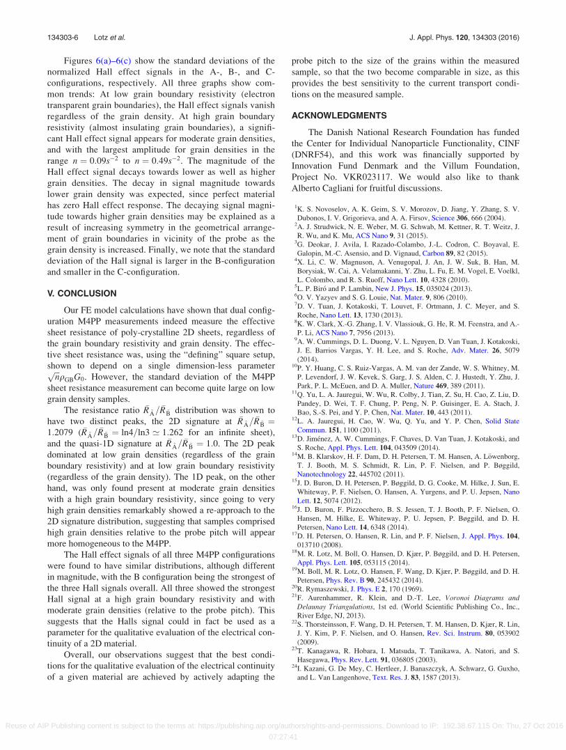
Figures 6(a)–6(c) show the standard deviations of the
normalized Hall effect signals in the A-, B-, and C-
configurations, respectively. All three graphs show com-
mon trends: At low grain boundary resistivity (electron
transparent grain boundaries), the Hall effect signals vanish
regardless of the grain density. At high grain boundary
resistivity (almost insulating grain boundaries), a signifi-
cant Hall effect signal appears for moderate grain densities,
and with the largest amplitude for grain densities in the
range n ¼ 0:09s�2 to n ¼ 0:49s�2. The magnitude of the
Hall effect signal decays towards lower as well as higher
grain densities. The decay in signal magnitude towards
lower grain density was expected, since perfect material
has zero Hall effect response. The decaying signal magni-
tude towards higher grain densities may be explained as a
result of increasing symmetry in the geometrical arrange-
ment of grain boundaries in vicinity of the probe as the
grain density is increased. Finally, we note that the standard
deviation of the Hall signal is larger in the B-configuration
and smaller in the C-configuration.
V. CONCLUSION
Our FE model calculations have shown that dual config-
uration M4PP measurements indeed measure the effective
sheet resistance of poly-crystalline 2D sheets, regardless of
the grain boundary resistivity and grain density. The effec-
tive sheet resistance was, using the “defining” square setup,
shown to depend on a single dimension-less parameterffiffiffi
np
qGBG0. However, the standard deviation of the M4PP
sheet resistance measurement can become quite large on low
grain density samples.
The resistance ratio �R ~A=�R ~B distribution was shown to
have two distinct peaks, the 2D signature at �R ~A=�R ~B ¼
1:2079 ( �R ~A=�R ~B ¼ ln4=ln3 ’ 1:262 for an infinite sheet),
and the quasi-1D signature at �R ~A=�R ~B ¼ 1:0. The 2D peak
dominated at low grain densities (regardless of the grain
boundary resistivity) and at low grain boundary resistivity
(regardless of the grain density). The 1D peak, on the other
hand, was only found present at moderate grain densities
with a high grain boundary resistivity, since going to very
high grain densities remarkably showed a re-approach to the
2D signature distribution, suggesting that samples comprised
high grain densities relative to the probe pitch will appear
more homogeneous to the M4PP.
The Hall effect signals of all three M4PP configurations
were found to have similar distributions, although different
in magnitude, with the B configuration being the strongest of
the three Hall signals overall. All three showed the strongest
Hall signal at a high grain boundary resistivity and with
moderate grain densities (relative to the probe pitch). This
suggests that the Halls signal could in fact be used as a
parameter for the qualitative evaluation of the electrical con-
tinuity of a 2D material.
Overall, our observations suggest that the best condi-
tions for the qualitative evaluation of the electrical continuity
of a given material are achieved by actively adapting the
probe pitch to the size of the grains within the measured
sample, so that the two become comparable in size, as this
provides the best sensitivity to the current transport condi-
tions on the measured sample.
ACKNOWLEDGMENTS
The Danish National Research Foundation has funded
the Center for Individual Nanoparticle Functionality, CINF
(DNRF54), and this work was financially supported by
Innovation Fund Denmark and the Villum Foundation,
Project No. VKR023117. We would also like to thank
Alberto Cagliani for fruitful discussions.
1K. S. Novoselov, A. K. Geim, S. V. Morozov, D. Jiang, Y. Zhang, S. V.
Dubonos, I. V. Grigorieva, and A. A. Firsov, Science 306, 666 (2004).2A. J. Strudwick, N. E. Weber, M. G. Schwab, M. Kettner, R. T. Weitz, J.
R. Wu, and K. Mu, ACS Nano 9, 31 (2015).3G. Deokar, J. Avila, I. Razado-Colambo, J.-L. Codron, C. Boyaval, E.
Galopin, M.-C. Asensio, and D. Vignaud, Carbon 89, 82 (2015).4X. Li, C. W. Magnuson, A. Venugopal, J. An, J. W. Suk, B. Han, M.
Borysiak, W. Cai, A. Velamakanni, Y. Zhu, L. Fu, E. M. Vogel, E. Voelkl,
L. Colombo, and R. S. Ruoff, Nano Lett. 10, 4328 (2010).5L. P. Bir�o and P. Lambin, New J. Phys. 15, 035024 (2013).6O. V. Yazyev and S. G. Louie, Nat. Mater. 9, 806 (2010).7D. V. Tuan, J. Kotakoski, T. Louvet, F. Ortmann, J. C. Meyer, and S.
Roche, Nano Lett. 13, 1730 (2013).8K. W. Clark, X.-G. Zhang, I. V. Vlassiouk, G. He, R. M. Feenstra, and A.-
P. Li, ACS Nano 7, 7956 (2013).9A. W. Cummings, D. L. Duong, V. L. Nguyen, D. Van Tuan, J. Kotakoski,
J. E. Barrios Vargas, Y. H. Lee, and S. Roche, Adv. Mater. 26, 5079
(2014).10P. Y. Huang, C. S. Ruiz-Vargas, A. M. van der Zande, W. S. Whitney, M.
P. Levendorf, J. W. Kevek, S. Garg, J. S. Alden, C. J. Hustedt, Y. Zhu, J.
Park, P. L. McEuen, and D. A. Muller, Nature 469, 389 (2011).11Q. Yu, L. A. Jauregui, W. Wu, R. Colby, J. Tian, Z. Su, H. Cao, Z. Liu, D.
Pandey, D. Wei, T. F. Chung, P. Peng, N. P. Guisinger, E. A. Stach, J.
Bao, S.-S. Pei, and Y. P. Chen, Nat. Mater. 10, 443 (2011).12L. A. Jauregui, H. Cao, W. Wu, Q. Yu, and Y. P. Chen, Solid State
Commun. 151, 1100 (2011).13D. Jim�enez, A. W. Cummings, F. Chaves, D. Van Tuan, J. Kotakoski, and
S. Roche, Appl. Phys. Lett. 104, 043509 (2014).14M. B. Klarskov, H. F. Dam, D. H. Petersen, T. M. Hansen, A. L€owenborg,
T. J. Booth, M. S. Schmidt, R. Lin, P. F. Nielsen, and P. Bøggild,
Nanotechnology 22, 445702 (2011).15J. D. Buron, D. H. Petersen, P. Bøggild, D. G. Cooke, M. Hilke, J. Sun, E.
Whiteway, P. F. Nielsen, O. Hansen, A. Yurgens, and P. U. Jepsen, Nano
Lett. 12, 5074 (2012).16J. D. Buron, F. Pizzocchero, B. S. Jessen, T. J. Booth, P. F. Nielsen, O.
Hansen, M. Hilke, E. Whiteway, P. U. Jepsen, P. Bøggild, and D. H.
Petersen, Nano Lett. 14, 6348 (2014).17D. H. Petersen, O. Hansen, R. Lin, and P. F. Nielsen, J. Appl. Phys. 104,
013710 (2008).18M. R. Lotz, M. Boll, O. Hansen, D. Kjær, P. Bøggild, and D. H. Petersen,
Appl. Phys. Lett. 105, 053115 (2014).19M. Boll, M. R. Lotz, O. Hansen, F. Wang, D. Kjær, P. Bøggild, and D. H.
Petersen, Phys. Rev. B 90, 245432 (2014).20R. Rymaszewski, J. Phys. E 2, 170 (1969).21F. Aurenhammer, R. Klein, and D.-T. Lee, Voronoi Diagrams and
Delaunay Triangulations, 1st ed. (World Scientific Publishing Co., Inc.,
River Edge, NJ, 2013).22S. Thorsteinsson, F. Wang, D. H. Petersen, T. M. Hansen, D. Kjær, R. Lin,
J. Y. Kim, P. F. Nielsen, and O. Hansen, Rev. Sci. Instrum. 80, 053902
(2009).23T. Kanagawa, R. Hobara, I. Matsuda, T. Tanikawa, A. Natori, and S.
Hasegawa, Phys. Rev. Lett. 91, 036805 (2003).24I. Kazani, G. De Mey, C. Hertleer, J. Banaszczyk, A. Schwarz, G. Guxho,
and L. Van Langenhove, Text. Res. J. 83, 1587 (2013).
134303-6 Lotz et al. J. Appl. Phys. 120, 134303 (2016)
Reuse of AIP Publishing content is subject to the terms at: https://publishing.aip.org/authors/rights-and-permissions. Download to IP: 192.38.67.115 On: Thu, 27 Oct 2016
07:27:41