Embed Size (px)
Citation preview

lable at ScienceDirect
Carbon 99 (2016) 591e598
Contents lists avai
Carbon
journal homepage: www.elsevier .com/locate/carbon
Metal-free chemical vapor deposition growth of graphitic tubularstructures on engineered perovskite oxide substrates
Jingyu Sun 1, Frank Dillon, Chen Wu 2, Jun Jiang, Kerstin Jurkschat, Antal A. Ko�os 3,Alison Crossley, Nicole Grobert**, Martin R. Castell*
University of Oxford, Department of Materials, Parks Road, Oxford, OX1 3PH, UK
a r t i c l e i n f o
Article history:Received 10 November 2015Received in revised form14 December 2015Accepted 26 December 2015Available online 29 December 2015
* Corresponding author.** Corresponding author.
E-mail addresses: [email protected]@materials.ox.ac.uk (M.R. Castell).
1 Current address: Cambridge Graphene Centre, UThomson Avenue, Cambridge CB3 0FA, United Kingdo
2 Current address: School of Materials Science andversity, Hangzhou 310027, China.
3 Current address: Centre for Energy Research, InstMaterials Science, Budapest 1121, Hungary.
http://dx.doi.org/10.1016/j.carbon.2015.12.0840008-6223/© 2015 Elsevier Ltd. All rights reserved.
a b s t r a c t
Metal-free growth of carbon nanotubes/fibers (CNT/Fs) using chemical vapor deposition (CVD) onsemiconducting and insulating substrates is of interest in the context of the construction of nanoscaleelectronic devices. However, controllable synthesis of CNT/Fs without the aid of metal catalysts is anongoing challenge. Here we report the direct CVD synthesis of CNT/Fs on the perovskite oxides SrTiO3
(STO) and Ba0.6Sr0.4TiO3 (BST). A variety of processing steps were used on STO (001) substrates to create aset of six patterns with varying atomic-scale surface roughnesses. These substrates were all subjected tothe same CVD growth conditions, and a correlation was found between the surface roughness of thesubstrates and the density of CNT/Fs. This indicates that nanometer-scale asperities on the substrates actas the catalytically active sites for CNT/F growth. In a separate set of experiments the surfaces of polishedpolycrystalline BST samples were investigated. The random orientation of the exposed etched facets ofthe individual grains revealed significantly different catalytic activity for CNT/F growth. Our studydemonstrates the great influence of the nature of the crystal surface condition on the catalytic activity ofthe substrates and is a critical first step towards perovskite oxide catalyst design.
© 2015 Elsevier Ltd. All rights reserved.
1. Introduction
Many evolving electronic technologies require low dimensionalcarbon materials such as graphene and carbon nanotubes or fibers(CNT/Fs) that are free from the residues of metal catalysts. Metal-catalyst-free growth of novel carbon nanomaterials has been ach-ieved to date by using chemical vapor deposition (CVD) processesin conjunction with oxides and nitrides as the catalysts materials[1e7]. For example, graphitic layers have been grown on MgOcrystals [8], graphene has been synthesized on SiO2 [9e13], Al2O3
[14,15] and glass [16e18] surfaces, and single-walled CNTs havebeen generated from SiO2 [19e21] and TiO2 [22,23] particles/
c.uk (N. Grobert), martin.
niversity of Cambridge, 9 JJm.Engineering, Zhejiang Uni-
itute of Technical Physics and
composites.Perovskite oxides, such as SrTiO3 (STO) and BaSrTiO3 (BST), are
important technological materials that are used as oxygen sensors[24], as electrodes in fuel cells [25], in tunable microwave systems[26], and as catalysis platforms [27,28]. Recently we reported that aBST substrate was able to accommodate the controlled growth ofcarbon helical structures [27] and a further study by Sun et al.demonstrated that high-quality monolayer graphene can be growndirectly onto STO single crystals via catalyst-free CVD [29].
In this paper we present the results of a series of experimentswhere CVD was used to synthesize CNT/Fs on the perovskite oxidesSTO and BST. The main result is that variations in the nanometer-scale surface structure give rise to differences in CNT/F yields thatvary by orders of magnitude. This insight will be a cornerstone inthe design of future perovskite oxide catalyst materials for thegrowth of graphitic tubular structures.
2. Experimental
2.1. STO (001) substrate engineering
Epi-polished STO (001) samples (PI-KEM Ltd, UK), doped with

J. Sun et al. / Carbon 99 (2016) 591e598592
0.5%wt Nb were used as substrates. An ultra-high vacuum (UHV)system, incorporating a treatment chamber, an Arþ ion sputtersource, and a scanning tunneling microscope (STM) [24], was usedfor the treatment and characterization of the substrates prior totheir transfer to the CVD growth apparatus. A series of STO (001)substrates with different surfaces structures was created as re-ported in detail in our previous papers [30e38]. Below we brieflysummarise the preparation conditions.
Sputtered: The as-received STO sample was first degassed, fol-lowed by Arþ ion bombardment with an ion energy of 0.75 keVand an ion flux of 1.28 A m�2 for 20 min. This procedure leads tothe roughest surface that was investigated.BHF-etched: The as-received STO sample was etched for 10 minin a buffered HF (NH4FeHF) solution (pH ¼ 4.5), in accordancewith the recipe described by Kawasaki et al. [39] This treatmentremoves any surface SrO layers resulting in a rough surface withonly TiO2 terminations.Degassed: The as-received STO sample was introduced into theUHV system and annealed at 600 �C for up to 1 h. This processproduces a relatively rough surface, but where most of thesurface contamination has been removed.(2�1)-reconstructed: This reconstructed surface was preparedby annealing the sample in UHV at 800 �C for 30 min.Nanostructured: The surface decorated with TiO2 nanostructureswas produced by Arþ ion sputtering (0.75 keV, 1 A m�2, 10 min)and subsequently annealing in UHV at 900 �C for 30 min.c(4�2)-reconstructed: The STO (001) c(4 � 2) reconstructedsurface was produced through Arþ ion sputtering (0.75 keV,1 A m�2, 10 min), followed by annealing at 1200 �C for 15 min.Scratched: To create the scratched STO substrates, as-receivedSTO samples were first etched in the BHF solution for 5 minand then scratched using a diamond scribe to avoid any metalcontamination. This procedure results in STO particles depositedaround the scratch site (Fig. S1, Supporting Information).
2.2. Polycrystalline BST substrate engineering
Epi-polished polycrystalline Ba0.6Sr0.4TiO3 substrates (PI-KEMLtd, UK) were used. The BST samples were etched for 10 min in theBHF solution, as described above, and then cleaned using ethanoland deionized water.
2.3. CVD procedure for the growth of CNT/Fs
For CNT/F growth, both EtOH-CVD and C2H2-CVD were carriedout on the STO and BST substrates. The substrates were insertedinto a quartz tube (2.2 cm inner diameter), which was then placedin a 50 cm long horizontal furnace. To ensure that the process wascompletely free of metal catalysts, a brand new quartz furnace tubewas employed for each CVD run, and plastic tools were used forsample handling. For EtOH-CVD, C2H5OH (Aldrich 99.5%) was usedas the carbon feedstock and was introduced via an ultrasonic piezo-driven aerosol generator (RBI Pyrosol 7901). In a typical CVDexperiment, C2H5OH was carried by an Ar/H2 mixture and intro-duced to the furnace tube after it had reached the growth tem-perature. After the growth, the furnace was switched off and thequartz tube was cooled down to room temperature in Ar. For C2H2-CVD, C2H2 (BOC, UK) as carbon feedstock was directly introducedalong with Ar and H2, the gas flow rate was always set at 20e40standard cubic centimetres per minute (sccm) for the duration ofgrowth. It is worth noting that the samples were subjected to an H2(800 sccm for 5 min) anneal at the growth temperature before theintroduction of the carbon feedstock (C2H5OH or C2H2).
2.4. Characterization
Prior to the CVD growth process, the set of STO (001) substrateswas characterized with an STM (JEOL JSTM 4500xt) using an elec-trochemically etched W tip with the bias voltage applied to thesample. The polycrystalline BST substrates were characterized us-ing an atomic force microscope (AFM) (Veeco Park CP AutoProbe)operated in tapping mode. Following the growth of the CNT/Fs, thesamples were analyzed in a JEOL JSM 840F scanning electron mi-croscope (SEM, 5 kV), and a JEOL JEM 4000HR transmission elec-tron microscope (TEM, 80 kV). The quality of the CNT/Fs wasdetermined by Raman spectroscopy using a JY Horiba LabramAramis imaging confocal Raman microscope with a 532 nm fre-quency doubled Nd:YAG laser. Electron backscatter diffraction(EBSD) measurements were performed in a JEOL JSM 6500F SEM at20 kV. White-light interferometric microscopy (Micro-XAM) datawere generated with an Omniscan Micro-XAM 5000B 3D instru-ment. Elemental analysis for the grown samples was performedusing energy-dispersive X-ray spectroscopy (EDX) in an SEM (JEOLJSM 840A) and a TEM (JEOL JEM 2010) TEM. X-ray photoelectronspectrometry (XPS) was performed with radiation from the Mg Kaband (hy¼ 1253 eV) using a VG Clam electron energy spectrometer.
3. Results and discussion
3.1. Surface-roughness-tailored growth of CNT/Fs on STO (001)substrates
Surface roughness studies were conducted by preparing a seriesof substrates that all exhibited different surface structures. Thesewere as follows: Arþ ion sputtered, BHF-etched, degassed, (2 � 1)-reconstructed, nanostructured and c(4 � 2)-reconstructed. Thepreparation processes are described in the experimental section.Fig. 1 shows typical STM images of the c(4� 2) (a1), nanostructured(b1) and sputtered (c1) surfaces in the left column and the corre-sponding representative SEM images following CNT/F growth inthe right column (a2-c2). The same growth conditions for all thesamples was EtOH-CVD in an Ar/H2 (400/200 sccm) atmosphere ata growth temperature of 700 �C for 30 min. The different surfacestructures clearly give rise to different yields of CNT/Fs. Theatomically flat c(4 � 2) reconstructed surface yields no measurableCNT/Fs and appears to be catalytically inert, whereas the Arþ ionsputtered sample produces a dense matt of CNT/Fs.
We carried out a detailed investigation of the Arþ ion sputteredsample, before and after CNT/F growth. The SEM, transmissionelectron microscopy TEM, and Raman spectroscopy results areshown in Fig. S2. The CNT/Fs had typical diameters between 8 and18 nm, an areal density of 3.4 � 109± 1.7 � 109 cm�2, and were ofgood quality considering the relatively low growth temperature of700 �C. To verify that a metal-catalyst-free growth process hadindeed taken place, XPS measurements were performed on thesputtered samples before and after CVD growth (Fig. S3), and nometal contaminants were found.
To investigate the relationship between the roughness of thesurfaces and their CNT/F yield, we carried out a detailed analysis ofthe samples with different surface structures. In addition to theimages from Fig. 1, the STM images of the BHF-etched, degassed,and (2 � 1)-reconstructed samples are shown next to their CNT/Fgrowths in Fig. S4. The areal root-mean-square (rms) surfaceroughness of the various STO substrate surfaces and the corre-sponding areal CNT/F count is plotted in Fig. 2. The rms surfaceroughness for each substrate was obtained by typically averagingthe results of 20 STM images. The values of the densities of CNT/Fswere obtained by analyzing the SEM micrographs. The errors(shown as error bars along both the x and y axes in the plot)

Fig. 1. Surface structure dependent CNT/F growth on SrTiO3 (001) substrates by directEtOH-CVD. Left column: STM images of (a1) c(4 � 2)-reconstructed, (b1) nano-structured, and (c1) sputtered substrates. Right column: (a2-c2) SEM images of CNT/Fsgrown on corresponding SrTiO3 substrates. (A color version of this figure can beviewed online).
Fig. 2. Plot of the areal rms surface roughness of the SrTiO3 (001) substrates versus theareal density of CNT/Fs grown on them by CVD. (A color version of this figure can beviewed online).
J. Sun et al. / Carbon 99 (2016) 591e598 593
represent the standard deviations of the measurements. The datapoint for the c(4 � 2)-reconstructed surface (rms roughness0.15 ± 0.07 nm) is not included in the plot because no CNT/Fs were
seen on this surface after the CVD process. It should also be pointedout that there was a significant variation in the yield obtained fromthe (2 � 1)-reconstructed samples, where some of these surfacesshowed a very low CNT/F yield. In Fig. 2 the (2 � 1) data point isonly made up from (2 � 1) surfaces where a meaningful measur-able yield was observed.
As can be readily seen in the plot, there is a strong correlationbetween the rms roughness of the surfaces of the samples and thelogarithm of the CNT/F density. This relationship leads us to spec-ulate that nanoscale STO surface asperities act as the nucleationsites for CNT/F growth. Highly ordered surfaces, such as theatomically flat c(4� 2) and (2� 1) reconstructed surfaces have veryfew asperities that are large enough to stimulate CNT/F growth. Incontrast, the Arþ ion sputtered surface has a broad range of as-perities of varying sizes and shapes that can readily act as CNT/Fnucleation sites.
Early work on laser-etched quartz substrates also suggested thatsurface roughness may play a significant role in the nucleationbehavior of multi-wall carbon nanotubes [40]. To further investi-gate the nature of STO asperities for stimulating CNT/F growth, wecarried out EtOH- and C2H2-CVD on STO scratched substrates.Scratching the STO surface prior to CVD using a diamond scribeleads to the generation of a surface containing nanometer- andmicron-sized STO particles with a variety of curvatures. For EtOH-CVD, our growth experiment was carried out at a temperature of700 �C. The samples were subsequently characterized by SEM, EDX,XPS and Raman spectroscopy, and indicate that CNT/Fs weregenerated from the scratching mark via a metal-catalyst-free pro-cess (Fig. S5). The results from the C2H2-CVD growth at 700 �C areshown in Fig. 3. The SEM micrograph in Fig. 3a shows the CNT/Fsthat grew on the scratched sample. The TEM image in Fig. 3b showsthat the formation of CNT/Fs occurs at the periphery of the white-circled particle marked with a “c”. EDX measurements from thecatalyst particle “c” are presented in Fig. 3c and show the presenceof the elements Sr, Ti, O, C, and Cu, which result from the SrTiO3catalyst particle, the carbon CNT/F, and the copper TEM grid(Fig. 3d). XPS measurements were also performed on the samples(Fig. 3e), and there is no indication of the presence of conventionaltypes of metal catalysts (e.g. Fe, Co, Ni). This study of the scratchedsurface complements the previous results on the set of STO (001)surfaces and provides further evidence that STO asperities andsmall particles act as catalysts for the nucleation of CNT/Fs duringCVD growth.
3.2. Facet-orientation-dictated growth of CNT/Fs on BST polycrystalsubstrates
So far we have shown how an STO crystal with the (001) crys-tallographic orientation can be modified in different ways to pro-duce surfaces that have different CNT/F yields. In the next part ofthe paper we show that the facet orientation of individual grainswithin a BST polycrystal is also a significant factor in catalyzing thenucleation and growth of CNT/Fs. The BST polycrystals weredelivered pre-polished and prior to carrying out our experimentswe etched them in a BHF solution. The etching treatment removesthe polishing damage and any metal nanoparticle contamination,giving rise to a clean polycrystalline BST surface with a large varietyof randomly oriented grain facets. These samples were character-ized by SEM, AFM and Micro-XAM as shown in Fig. S6, which showtypical grain diameters of the order of a few mm. To grow CNT/Fs onthe etched BST samples, EtOH-CVD and C2H2-CVD were employedat a growth temperature of 750 �C with mixed carrier gases (Ar/H2:500/500 sccm) flowing during the reaction. EDX and XPS analysesfor the etched and post-grown samples were performed to verifythat a metal-catalyst-free CVD process had taken place (Fig. S7).

Fig. 3. Characterization of CNT/Fs grown on scratched SrTiO3 surfaces by C2H2-CVD at a growth temperature of 700 �C. (a) SEM and (b) TEM observations of the grown sample. Scalebars: (a) 500 nm. (b) 20 nm. (c,d) EDX spectra of the white-circled regions in (b). The EDX spectrum (c) of the catalytic nanoparticle trapped within the tube demonstrates that it isSrTiO3. The EDX spectrum (d) of the TEM grid shows the Cu background signal. (e) XPS spectrum of the as-grown sample showing a surface that is free frommetallic species such asFe, Co, Ni and Cu.
J. Sun et al. / Carbon 99 (2016) 591e598594
The influence of the facet orientation of the grains on the CNT/Fyield can be clearly seen in the SEM image library shown in Fig. 4.Some facets support prolific growth of CNT/Fs, whereas other facetsproduce nothing at all. Fig. 4a and b are SEM images at differentmagnifications, which show the growth of CNT/Fs on the BSTpolycrystalline surface by EtOH-CVD. Similar growth behavior wasobserved when C2H2-CVD was used (Fig. 4c and d). Shorter growthtimes of 30 s were also tested (Fig. 4e and f) and showostensibly thesame result, namely that the CNT/Fs nucleation sites vary consid-erably depending on the grain facets. The influence of grain ori-entations has been investigated in detail by us with respect to theCVD growth of graphene on Cu foil [41]. The quality of the as-grownCNT/Fs was evaluated by Raman spectroscopy. The representativeRaman spectrum of the sample (Fig. 5) displays the three charac-teristic peaks of graphitic tubular structures at the D (~1350 cm�1),G (~1580 cm�1) and 2D bands (~2690 cm�1), confirming the highpurity of samples prepared in this work. It is worth-mentioningthat the Raman spectrum of a carbon nanotube displays a 2Dpeak similar to that of graphene, which is not too surprising as it isregarded as a rolled up sheet of graphene. The 2D band is thesecond order of the D band, which is due to double resonance,linking the phonon wavevectors to the electronic band structure[42]. The importance of Raman 2D band for carbon nanomaterialslies in the fact that it can be efficiently used to monitor the number
of layers for graphene [43] as well as to distinguish the doping typeof carbon nanotube [44].
The intensity of G band relative to that of the D band (IG/ID) isoften used as a measure of the quality with nanotubes, where acomparison between obtained and published results is meaningfulto characterize the sample quality. The calculated IG/ID ratio in Fig. 5is ~1.2, indicating that the carbon nanostructures are indeed CNT/Fsbut contain many defects. Representative results on the growth ofCNT/Fs over non-metallic catalysts are summarized in Table 1, withthe highlight of Raman IG/ID ratio. Note that our growth werenormally carried out at low reaction temperatures (i.e. <800 �C)during metal-free CVD processes, the conditions of which areconsistent with the results reported in Refs. [46,47]. Our futurework would aim at the enhancement of CNT growth quality byincreasing the reaction temperature and/or designing perovskiteoxide catalyst nanoparticles.
To further probe the phenomenon of facet-related growthbehavior, SEM, electron backscatter diffraction (EBSD) and Micro-XAM were used to co-investigate the same regions of the samplefollowing CNT/F growth. Fig. 6aec depict an area of interest, wherethe center of the images represent the same triple-junction. TheSEM image in Fig. 6a displays facet-selective growth of CNT/Fs onthe three grain facets. The facets numbered 1 and 3 contain asubstantial number of CNT/Fs, whereas facet 2 does not support
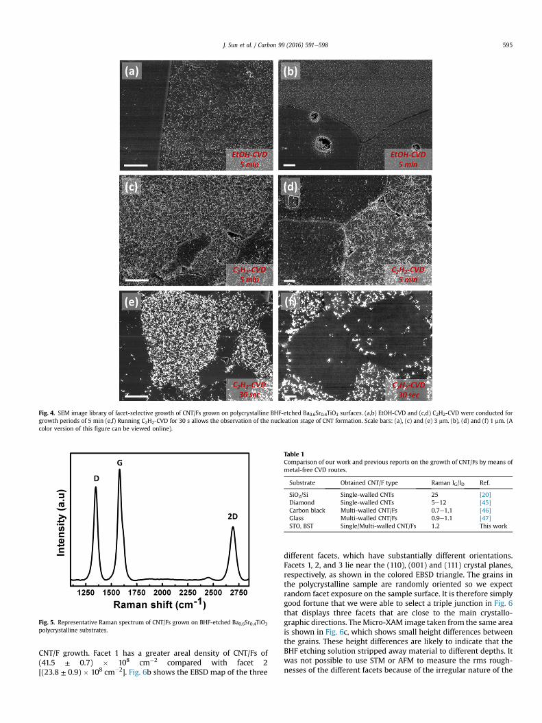
Fig. 4. SEM image library of facet-selective growth of CNT/Fs grown on polycrystalline BHF-etched Ba0.6Sr0.4TiO3 surfaces. (a,b) EtOH-CVD and (c,d) C2H2-CVD were conducted forgrowth periods of 5 min (e,f) Running C2H2-CVD for 30 s allows the observation of the nucleation stage of CNT formation. Scale bars: (a), (c) and (e) 3 mm. (b), (d) and (f) 1 mm. (Acolor version of this figure can be viewed online).
Fig. 5. Representative Raman spectrum of CNT/Fs grown on BHF-etched Ba0.6Sr0.4TiO3
polycrystalline substrates.
Table 1Comparison of our work and previous reports on the growth of CNT/Fs by means ofmetal-free CVD routes.
Substrate Obtained CNT/F type Raman IG/ID Ref.
SiO2/Si Single-walled CNTs 25 [20]Diamond Single-walled CNTs 5e12 [45]Carbon black Multi-walled CNT/Fs 0.7e1.1 [46]Glass Multi-walled CNT/Fs 0.9e1.1 [47]STO, BST Single/Multi-walled CNT/Fs 1.2 This work
J. Sun et al. / Carbon 99 (2016) 591e598 595
CNT/F growth. Facet 1 has a greater areal density of CNT/Fs of(41.5 ± 0.7) � 108 cm�2 compared with facet 2[(23.8 ± 0.9) � 108 cm�2]. Fig. 6b shows the EBSD map of the three
different facets, which have substantially different orientations.Facets 1, 2, and 3 lie near the (110), (001) and (111) crystal planes,respectively, as shown in the colored EBSD triangle. The grains inthe polycrystalline sample are randomly oriented so we expectrandom facet exposure on the sample surface. It is therefore simplygood fortune that we were able to select a triple junction in Fig. 6that displays three facets that are close to the main crystallo-graphic directions. TheMicro-XAM image taken from the same areais shown in Fig. 6c, which shows small height differences betweenthe grains. These height differences are likely to indicate that theBHF etching solution stripped away material to different depths. Itwas not possible to use STM or AFM to measure the rms rough-nesses of the different facets because of the irregular nature of the

Fig. 6. (a) SEM, (b) EBSD and (c) Micro-XAM co-investigation of facet-selective growthof CNT/Fs on a BHF-etched Ba0.6Sr0.4TiO3 polycrystalline surface. The images weretaken from the same triple-junction on the sample. The numbers marked on eachimage indicate the three different grain facets. A color triangle, used to index the EBSDmap in (b), is also shown in (d). Scale bars: (a) 1 mm. (b) 5 mm. (c) 2 mm. (A color versionof this figure can be viewed online).
Fig. 7. (a1-c1) SEM overviews of three different areas of the Ba0.6Sr0.4TiO3 polycrystal followinMicro-XAM co-investigations of facet-selective growth of CNT/Fs with each row correspondincrystal facets for each position. The CNT/F growth on the facets marked by yellow-colored nbars: (a1-c1) 5 mm. (a2-c2) 1 mm. (a3-c3) 5 mm. (a4-c4) 10 mm. (A color version of this figure
J. Sun et al. / Carbon 99 (2016) 591e598596
polycrystalline surface that included pinholes. However, it isreasonable to assume that the different facets respond differentlyto the BHF etching process, resulting in different roughnesses onthe grain surfaces. As shown earlier for the STO (001) sample aswell as in other studies [19,48], surface roughness is one of theparamount factors for producing CNT/Fs within a catalyst-freeprocess. The (001) surface is generally the most stable in perov-skite oxides, and will therefore likely to result in a smooth surfacefollowing the BHF etch. It is therefore not surprising that facet 2 inFig. 6, which lies near the (001) orientation has the lowest CNT/Fyield.
Fig. 7 shows a further set of results from SEM, EBSD and Micro-XAM co-investigations of three different areas on the sample. TheCNT/F growth on the facets marked by yellow-colored numbers inFig. 7a1-c1 are shown in the high-magnification SEM images inFig. 7a2-c2. The EBSD maps are shown in Fig. 7a3-c3 and the Micro-XAM images in Fig. 7a4-c4. Qualitative investigation of the data inFig. 7 indicates that facets that are near the (001) orientation (redin a3-c3) have the lowest CNT/F yield. Specifically these facets arenumbers 2 and 4 in (a3) and facet 3 in (b3). In contrast, facets nearthe (110) orientation (green in in a3-c3) have relatively high CNT/Fyields. This finding is in agreement with the results of Fig. 6. TheMicro-XAM images in Fig. 7 serve to demonstrate the differentetching rates on the grains. For example, in (a4) grain 2 is96 ± 27 nm higher than neighboring grain 4. We do not have asufficiently exhaustive data set to attempt a quantitative analysisof the data in Fig. 7, but feel that there is enough evidence tospeculate that the BHF etch results in different surface rough-nesses on the different facets and that this is responsible for thevarying CNT/F yields. Further, the facets near the stable (001)orientation ought to be the smoothest and therefore have thelowest yields.
g CNT/F growth. (a2-c2) High magnification SEM of the CNT/Fs. (a3-c3) EBSD and (a4-c4)g to the same site of interest. The numbers marked on the images indicate the differentumbers are correspondingly shown in the high-magnified SEM images in (a2-c2). Scalecan be viewed online).

J. Sun et al. / Carbon 99 (2016) 591e598 597
4. Conclusions
In summary we have demonstrated that perovskite oxides canserve as effective catalysts to initiate the growth of CNT/Fs by adirect CVD route. Based on this observation, we developed a seriesof approaches to engineer the surfaces of STO (001) single crystalsto achieve roughness-tailored growth of CNT/Fs. We also demon-strated facet-orientation-selective growth of CNT/Fs on BST poly-crystalline substrates, and speculate that the surface roughness dueto the BHF etching process is similarly the key element in deter-mining CNT/F yield. This work shows that the nanoscale surfaceroughness of perovskite oxides is central to controlling the catalyticreactivity and hence the yield for CNT/F growth. This result is amilestone in the understanding of the design of future non-metalcatalysts for CNT/F synthesis.
Acknowledgments
We are grateful to the Royal Society (NG), European Commun-ity's Sixth and Seventh Framework Programme [DEDIGROWTH(ERC-2009-StG-240500); CONTACT (Marie-Curie-ITN-238263),BNC Tubes (FP6-NMP-033350)] (NG) and Chinese Ministry ofEducation-University of Oxford Scholarship (JS) for financial sup-port. We also thank Chris Spencer (JEOL, UK) for valuable STMtechnical support and Xiao Hu (Oxford Materials, UK) for EDX dataprocessing.
Appendix A. Supplementary data
Supplementary data related to this article can be found at http://dx.doi.org/10.1016/j.carbon.2015.12.084.
References
[1] A. Nel, T. Xia, L. Madler, N. Li, Toxic potential of materials at the nanolevel,Science 311 (5761) (2006) 622e627.
[2] M.H. Rümmeli, C. Kramberger, A. Gruneis, P. Ayala, T. Gemming, B. Buchner, etal., On the graphitization nature of oxides for the formation of carbon nano-structures, Chem. Mater. 19 (17) (2007) 4105e4107.
[3] G. Hong, Y. Chen, P. Li, J. Zhang, Controlling the growth of single-walledcarbon nanotubes on surfaces using metal and non-metal catalysts, Carbon50 (6) (2012) 2067e2082.
[4] K.S. Novoselov, V.I. Fal'ko, L. Colombo, P.R. Gellert, M.G. Schwab, K. Kim,A roadmap for graphene, Nature 490 (7419) (2012) 192e200.
[5] D. Jariwala, V.K. Sangwan, L.J. Lauhon, T.J. Marks, M.C. Hersam, Carbonnanomaterials for electronics, optoelectronics, photovoltaics, and sensing,Chem. Soc. Rev. 42 (7) (2013) 2824e2860.
[6] L.L. Tan, W.J. Ong, S.P. Chai, A.R. Mohamed, Growth of carbon nanotubes overnon-metallic based catalysts: a review on the recent developments, Catal.Today 217 (2013) 1e12.
[7] J. Sun, Y. Zhang, Z. Liu, Direct chemical vapor deposition growth of grapheneon insulating substrates, ChemNanoMat (2016), http://dx.doi.org/10.1002/cnma.201500160.
[8] M.H. Rümmeli, A. Bachmatiuk, A. Scott, F. Borrnert, J.H. Warner, V. Hoffman, etal., Direct low-temperature nanographene CVD synthesis over a dielectricinsulator, ACS Nano 4 (7) (2010) 4206e4210.
[9] J. Chen, Y. Wen, Y. Guo, B. Wu, L. Huang, Y. Xue, et al., Oxygen-aided synthesisof polycrystalline graphene on silicon dioxide substrates, J. Am. Chem. Soc.133 (44) (2011) 17548e17551.
[10] H. Bi, S. Sun, F. Huang, X. Xie, M. Jiang, Direct growth of few-layer graphenefilms on SiO2 substrates and their photovoltaic applications, J. Mater. Chem.22 (2) (2012) 411e416.
[11] J. Chen, Y. Guo, L. Jiang, Z. Xu, L. Huang, Y. Xue, et al., Near-equilibriumchemical vapor deposition of high-quality single-crystal graphene directly onvarious dielectric substrates, Adv. Mater. 26 (9) (2014) 1348e1353.
[12] Y.S. Kim, K. Joo, S.K. Jerng, J.H. Lee, E. Yoon, S.H. Chun, Direct growth ofpatterned graphene on SiO2 substrates without the use of catalysts orlithography, Nanoscale 6 (17) (2014) 10100e10105.
[13] Q. Liu, Y. Gong, T. Wang, W.L. Chan, J. Wu, Metal-catalyst-free and controllablegrowth of high-quality monolayer and AB-stacked bilayer graphene on silicondioxide, Carbon 96 (2016) 203e211.
[14] H.J. Song, M. Son, C. Park, H. Lim, M.P. Levendorf, A.W. Tsen, et al., Large scalemetal-free synthesis of graphene on sapphire and transfer-free device fabri-cation, Nanoscale 4 (10) (2012) 3050e3054.
[15] J. Hwang, M. Kim, D. Campbell, H.A. Alsalman, J.Y. Kwak, S. Shivaraman, et al.,van der Waals epitaxial growth of graphene on sapphire by chemical vapordeposition without a metal catalyst, ACS Nano 7 (1) (2013) 385e395.
[16] J. Sun, Y. Chen, M.K. Priydarshi, Z. Chen, A. Bachmatiuk, Z. Zou, et al., Directchemical vapor deposition-derived graphene glasses targeting wide rangedapplications, Nano Lett. 15 (9) (2015) 5846e5854.
[17] J. Sun, Y. Chen, X. Cai, B. Ma, Z. Chen, M.K. Priydarshi, et al., Direct low-temperature synthesis of graphene on various glasses by plasma-enhancedchemical vapor deposition for versatile, cost-effective electrodes, Nano Res.8 (11) (2015) 3496e3504.
[18] Y. Chen, J. Sun, J. Gao, F. Du, Q. Han, Y. Nie, et al., Growing uniform graphenedisks and films on molten glass for heating devices and cell culture, Adv.Mater. 27 (47) (2015) 7839e7846.
[19] S.M. Huang, Q.R. Cai, J.Y. Chen, Y. Qian, L.J. Zhang, Metal-catalyst-free growthof single-walled carbon nanotubes on substrates, J. Am. Chem. Soc. 131 (6)(2009) 2094e2095.
[20] B.L. Liu, W.C. Ren, L.B. Gao, S.S. Li, S.F. Pei, C. Liu, et al., Metal-catalyst-freegrowth of single-walled carbon nanotubes, J. Am. Chem. Soc. 131 (6) (2009)2082e2083.
[21] B.L. Liu, D.M. Tang, C.H. Sun, C. Liu, W.C. Ren, F. Li, et al., Importance of oxygenin the metal-free catalytic growth of single-walled carbon nanotubes fromSiOx by a vapor-solid-solid mechanism, J. Am. Chem. Soc. 133 (2) (2011)197e199.
[22] L. Kang, Y. Hu, L. Liu, J. Wu, S. Zhang, Q. Zhao, et al., Growth of close-packedsemiconducting single-walled carbon nanotube arrays using oxygen-deficient TiO2 nanoparticles as catalysts, Nano Lett. 15 (1) (2015) 403e409.
[23] W.J. Ong, M.M. Gui, S.P. Chai, A.R. Mohamed, Direct growth of carbon nano-tubes on Ni/TiO2 as next generation catalysts for photoreduction of CO2 tomethane by water under visible light irradiation, RSC Adv. 3 (14) (2013)4505e4509.
[24] W. Menesklou, H.J. Schreiner, K.H. Hardtl, E. Ivers-Tiffee, High temperatureoxygen sensors based on doped SrTiO3, Sens. Actuat B Chem. 59 (2e3) (1999)184e189.
[25] J.C. Ruiz-Morales, J. Canales-Vazquez, C. Savaniu, D. Marrero-Lopez, W.Z. Zhou,J.T.S. Irvine, Disruption of extended defects in solid oxide fuel cell anodes formethane oxidation, Nature 439 (7076) (2006) 568e571.
[26] J. Im, O. Auciello, S.K. Streiffer, Layered barium strontium titanate thin filmsfor high frequency tunable devices, Thin Solid Films 413 (1e2) (2002)243e247.
[27] J. Sun, A.A. Koos, F. Dillon, K. Jurkschat, M.R. Castell, N. Grobert, Synthesis ofcarbon nanocoil forests on BaSrTiO3 substrates with the aid of a Sn catalyst,Carbon 60 (2013) 5e15.
[28] J. Sun, C. Wu, F. Silly, A.A. Koos, F. Dillon, N. Grobert, et al., Controlled growthof Ni nanocrystals on SrTiO3 and their application in the catalytic synthesis ofcarbon nanotubes, Chem. Commun. 49 (36) (2013) 3748e3750.
[29] J. Sun, T. Gao, X. Song, Y. Zhao, Y. Lin, H. Wang, et al., Direct growth of high-quality graphene on high-k dielectric SrTiO3 substrates, J. Am. Chem. Soc. 136(18) (2014) 6574e6577.
[30] M.R. Castell, Nanostructures on the SrTiO3 (001) surface studied by STM, Surf.Sci. 516 (1e2) (2002) 33e42.
[31] M.R. Castell, Scanning tunneling microscopy of reconstructions on the SrTiO3(001) surface, Surf. Sci. 505 (2002) 1e13.
[32] F. Silly, M.R. Castell, Selecting the shape of supported metal nanocrystals: Pdhuts, hexagons, or pyramids on SrTiO3 (001), Phys. Rev. Lett. 94 (4) (2005)046103.
[33] D.S. Deak, F. Silly, D.T. Newell, M.R. Castell, Ordering of TiO2-based nano-structures on SrTiO3 (001) surfaces, J. Phys. Chem. B 110 (18) (2006)9246e9251.
[34] M.S.J. Marshall, A.E. Becerra-Toledo, L.D. Marks, M.R. Castell, Surface anddefect structure of oxide nanowires on SrTiO3, Phys. Rev. Lett. 107 (8) (2011)086102.
[35] M.S.J. Marshall, A.E. Becerra-Toledo, D.J. Payne, R.G. Egdell, L.D. Marks,M.R. Castell, Structure and composition of linear TiOx nanostructures onSrTiO3 (001), Phys. Rev. B 86 (12) (2012) 125416.
[36] A.E. Becerra-Toledo, M.S.J. Marshall, M.R. Castell, L.D. Marks, c(4�2) andrelated structural units on the SrTiO3 (001) surface: Scanning tunneling mi-croscopy, density functional theory, and atomic structure, J. Chem. Phys. 136(21) (2012) 214701.
[37] A.E. Becerra-Toledo, M.R. Castell, L.D. Marks, Water adsorption on SrTiO3(001): I. Experimental and simulated STM, Surf. Sci. 606 (7e8) (2012)762e765.
[38] D.T. Newell, A. Harrison, F. Silly, M.R. Castell, SrTiO3 (001)-(sqrt5 � sqrt5)-R26.6� reconstruction: a surface resulting from phase separation in a reducingenvironment, Phys. Rev. B 75 (20) (2007) 205429.
[39] M. Kawasaki, K. Takahashi, T. Maeda, R. Tsuchiya, M. Shinohara, O. Ishiyama,et al., Atomic control of the SrTiO3 crystal surface, Science 266 (5190) (1994)1540e1542.
[40] N. Grobert, Novel Carbon Nanostructures, University of Sussex, 2000. PhDthesis.
[41] A.T. Murdock, A.A. Koos, T.B. Britton, L. Houben, T. Batten, T. Zhang, et al.,Controlling the orientation, edge geometry, and thickness of chemical vapordeposition graphene, ACS Nano 7 (2) (2013) 1351e1359.
[42] A.C. Ferrari, Raman spectroscopy of graphene and graphite: disorder,electron-phonon coupling, doping and nonadiabatic effects, Solid StateCommun. 143 (1e2) (2007) 47e57.

J. Sun et al. / Carbon 99 (2016) 591e598598
[43] A.C. Ferrari, J.C. Meyer, V. Scardaci, C. Casiraghi, M. Lazzeri, F. Mauri, et al.,Raman spectrum of graphene and graphene layers, Phys. Rev. Lett. 97 (18)(2006) 187401.
[44] I.O. Maciel, N. Anderson, M.A. Pimenta, A. Hartschuh, H. Qian, M. Terrones, etal., Electron and phonon renormalization near charged defects in carbonnanotubes, Nat. Mater. 7 (11) (2008) 878e883.
[45] D. Takagi, Y. Kobayashi, Y. Homma, Carbon nanotube growth from diamond,J. Am. Chem. Soc. 131 (20) (2009) 6922e6923.
[46] Z.Y. Zeng, J.H. Lin, Metal-catalyst-free growth of carbon nanotubes/carbon
nanofibers on carbon blacks using chemical vapor deposition, RSC Adv. 4 (76)(2014) 40251e40258.
[47] J.K. Seo, H. Jung, J.H. Lee, S.Y. Deok, J.J. Young, W.S. Choi, Metal-free CNTsgrown on glass substrate by microwave PECVD, Curr. Appl. Phys. 10 (3) (2010)S447eS450.
[48] J.H. Lin, C.S. Chen, M.H. Rümmeli, A. Bachmatiuk, Z.Y. Zeng, H.L. Ma, et al.,Growth of carbon nanotubes catalyzed by defect-rich graphite surfaces, Chem.Mater. 23 (7) (2011) 1637e1639.