Embed Size (px)
Citation preview
SC-R-65-941
METHODS FOR MEASURING AND CHARACTERIZING
TRANSISTOR AND DIODE LARGE SIGNAL PARAMETERS
FOR USE IN AUTOMATIC CIRCUIT ANALYSIS PROGRAMS
by
W. H. Sullivan
and
J. L. Wirth
JULY 1965
I
DISCLAIMER
This report was prepared as an account of work sponsored by an agency of the United States Government. Neither the United States Government nor any agency Thereof, nor any of their employees, makes any warranty, express or implied, or assumes any legal liability or responsibility for the accuracy, completeness, or usefulness of any information, apparatus, product, or process disclosed, or represents that its use would not infringe privately owned rights. Reference herein to any specific commercial product, process, or service by trade name, trademark, manufacturer, or otherwise does not necessarily constitute or imply its endorsement, recommendation, or favoring by the United States Government or any agency thereof. The views and opinions of authors expressed herein do not necessarily state or reflect those of the United States Government or any agency thereof.

DISCLAIMER
Portions of this document may be illegible in electronic image products. Images are produced from the best available original document.
Preprinted for: IEEE Annual Conference on Nuclear and Space Radiation Effects, July 12-15, 1965, Ann Arbor, Michigan.
Issued by Sandia Corporation,
a prime contractor to the United States Atomic Energy Commission
,-------- L E GA L N 0 T I C E -----~-, This report was prepo1red as an account of Government sponsored work.
Neither the United States, nor the Commission, nor any person acting on behalf of the Commission:
A. Makes any warr&flty or representation, expressed or implied, with respect to the accuracy, completeness, or uaerutness of the information contained In this report. or that the uae of any information, apparatus, method, or process disclosed in this report may not ln!rlnie priva.tely owned rigbta; or
B. Assumes any Habttlties wtth respect to the use of, or ror damages resulting !rom the use of any information, apparatus, method, or process disclosed in this report.
As used tn the above, "person actinlf on behalf of the Commission• i.ncludes any employee or contractor of the Commlsalon, or employee of sucb. contractor, to the extent that such employee or contractor ot the Commission.. or employee of such contractor prepa.res. diaseminatea, or provides access to, any Information pursuant to his employment or contract with the Commission, or his employment with such contractor.

) ,.
SANDIA CORPORATION REPRINT
METHODS FOR MEASURING AND CHARACTERIZING TRANSISTOR AND DIODE LARGE SIGNAL PARAMETERS FOR USE IN
AUTOMATIC CIRCUIT ANALYSIS PROGRAMS
by
W. H. Sullivan
and
J, L. Wirth
July 1965
SC-R-65-941
1
2
Summary
Introduction
Carrier Storage Models
Storage Parameter- Measurements
Permanent Damage Models
Conclusion
Acknowledgment
APPENDIX I.
Definition· of Symbols
References
TABLE OF CONTENTS
LIST OF ILLUSTRATIONS
Figure
la. Diode Equivalent Circuit
lb. Ebers-Moll Equivalent Circuit for an NPN Transistor
2. Diode Recovery Test Circuit
3a. Diode Recovery Waveforms
3b. Junction Capacitance Versus Voltage
3c. Collector Junction Depletion Capacitance Versus Junction Voltage
4. Theoretical and Experimental Recovery Waveforms
5. ·computed Recovery Waveforms for Models of Various Order
6a. Transistor Test Circuit
6b. Typical Transistor Recovery Waveforms
7a. Normal and Inverted hFE Versus Neutron Flux
7b. Junction Leakage Currents and Boltzmann Coefficients Versus Neutron Flux
7c. Normalized Collector and Emitter Capacitance Coefficient Versus Neutron Flux
I. 1. Base-Collector Current Ratio Versus Collector Voltage for Fixed Collector Current
I. 2a. Current Gain Versus Base-Emitter Voltage
I. 2b. Collector Multiplication Ratio Versus Collector Voltage
Page
::l
3
3
·s
10
ii
12
13
16
17
5
5
6
6
7
7
8
8
8
8
11
11
11
14
15
15

METHODS FOR MEASURING AND CHARACTERIZING TRANSISTOR AND DIODE LARGE SIGNAL PARAMETERS FOR USE IN
AUTOMATIC CIRCUIT ANALYSIS PROGRAMS*
Summary
The. mathematical bases of the Ebers- Moll, Charge-Control and Linvill models .are discussed in order to establish the parameter requirements and the accuracy of these models, A recovery technique for measuring those parameters associated with minority carrier storage in devices is described and typical values are given for several high frequency devices. Other parameters, such as current gain and junction depletion capacitance, do not require special measurement procedures and in these cases the characterization of the bias dependence of the parameter is given primary emphasis. The use of the recovery technique in characterizing permanent radiation (neutron) damage and in studying damage mechanisms in transistors is also discussed.
Introduction
Although the analysis and design of electronic circuits has been greatly simplified by computer programs,l, 2, 3 the choice of component models and the measurement of model parameters must still be made by the engineer. Therefore, the efficient use of these programs requires that the engineer be aware of the approximations inherent in the various device models as well as the techniques for determining the model parameters from laboratory measurements.
This paper considers the modeling problem in three steps. First, the mathematical bases of the Ebers-Mon,4 Charge-Control,5 and Linvill6 models are presented in order to establish the parameter requirements and inherent approximations of these models. Next, a recovery technique for measuring storage parameters, i.e., those parameters associated with the storage of minority carriers in the various regions of a device is presented and storage parameter values are reported for several devices, Other parameters, e. g., current gain and junction depletion capacitance, can be easily measured with standard laboratory equipment and consequently the
measurement of these parameters is not discussed in detail. However, the functional rela-
tions between these parameters and the device operating point is important, and this subject is discussed in Appendix I. Finally, the use of storage parameter measurements in the investigation of neutron damage in devices and materials is discussed.
Carrier Storage Models
At high current -levels the transient response of diodes and transi~tors is determined primarily by the effects of minority carri~r storage in the various regions of. the device. Although these effects can be modeled quite accurately by the continuity and diffusion equations, these equations are not particularly useful in circuit analysis work because of the difficulty in obtaining numerical solutions for arbitrary boundary conditions. Consequently, different approaches for approximating these "equations have evolved and form the nucleus for the various models.
Ebers-Moll and Charge-Control Models
The Ebers-Moll and Charge-Control models assume that the device has a one-dimensional geometry and the spatial distribution of minority carriers has a fixed form which is independent of· time, voltage, current, etc. Under these assumptions the total minority carrier charge stored in any region is linearly related to the carrier densities at the boundaries of that region. Therefore the excess charge, QAB· stor.ed in the region between surfaces A and B by minority carrier Z is given by
where ZA is· the carrier density at surface A, ZB is the density at surface B, Z 0 is the equilibrium density, and K1 and K2 are proportionality constants. The time variation of QAB can be determined by integrating the continuity equation
':'This work was supported by the United States Atomic Energy Commission. Reproduction in whole or in part is permitted for any purpose of the U. S. Government.
3
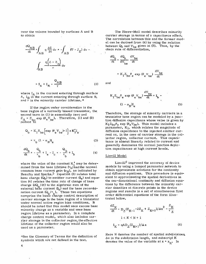
over the volume bounded by surfaces A and B to obtain
dQAB { az f · --= q - dv = - (\7 • J ) dv -dt AB dt AB Z
I _1~dv AB T
QAB =I +I---
A R T (2)
where IA is the current entering through surface A, In is the current entering through surface B, ::1nd T is the minority carrier lifetime. *
If the region under consideration is the base region of a normally biased transistor, the second term in (1) is essentially zero and ZA = Zbo exp (Be Vbe) •. Therefore, (1) and (2) reduce to ·
(3)
(4)
where the value of the constant K; may be determined from the base lifetime (Tb) and the normal common base current gain (aN)• as indicated by Beaufoy and Sparks.5 Equation (3) relates total base charge (Qb) to emitter current (Ie) and equation (4) relates the time rate of change of base charge (dQb/dt) to the algebraic sum of the external base current (Ib) and the base recombination current (Qb/T ). These two equations comprise the baslC clbarge control description of carrier storage in the base region of a transistor under normal active region bias conditions. It should be noted that this model uses excess base minority charge as a variable and uses base region lifetime as a parameter. In a complete charge control model, which a1so includes carrier storage in the collector region, the effective lifetime of the collector region would also be used as a parameter.
*See the Glossary of Terms for the definition of symbols which are not defined in the text.
4
The Ebers-Moll model describes minority carrier storage in terms of a capacitance effect. The correlation between this and the former model can be derived from (4) by using the relation between Qb and Vbe given in (3). Thus, by the chain rule of differentiation,
::l.nd
dVbe = K 1zb B exp (B v ) o e e be .dt
(5)
Therefore, the storage of minority carriers. in a transistor base region can be modeled by a junction diffusion capacitance whose value is given by K1ZboBe exp (Be Vbe>· This model includes a parameter, K1, which relates the magnitude of diffusion capacitance to the injected.emitter current or, in the case of carrier storage in the collector region, collector current. This capacitance is aimost linearly related to current and generally dominates the normal junction depletion capacitances at high current levels.
Linvill Model
Linvill6 improved the accuracy of device models by using a lumped parameter network to obtain approximate solutions for the -~ontinuity and diffusion equations. This procedure is equivalent to approximating the spatial derivatives in the one-dimensional continuity and diffusion equations by the difference between the minority carrier densities at discrete .points in the device regions and results in a set of simultaneous first order differential equations of the form illustrated below.
l<K<N+l
(6)
Here N denotes the number of spatial subdivisions, t:.x is the subdivision length, and subscript K denotes the value of the variable at x = xK. In

addition to the lifetimP. parameter introduced in the previous models, this model is also strongly dependent upon diffusivity, Dz, as well as the geometrical parameter 6x. The Linvill model therefore requires considerably more knowledge about the device structure than the previous models. However, this added detail does provide for a more accurate model.
Although the above derivations are neces- · sarily brief, they are included here 'to introduce the parameters containedln the various models and to review the approximations which are implicit in these rriodels. It should be apparent that, although the mathematical forms retained in the Charge-Control and Ebers-Moll models are different, these models result from a common mathematical basis and. consequently param-
. eter values for one model can be converted to the parameters of the other. This paper, therefore, deals exclusively with the Ebers- Moll and Linvill models. In addition, _the model derivations presented above deal exclusively with the carrier .storage problem. A complete device-model must also include junction depletion capacitance, bulk resistance, etc. These additions are shown schematically in Figure 1, where the Ebers-Moll .model of a diode and transistor are shown. The reader is referred to reference 6 for added detail on the Linvill model.
Storage -Pa-rameter-· Measurements
Storage parameters can be evaluated by either small signal reactance and-transfer function measurements or by transient response methods. Althou·gh the small signal methods are well known, and generally provide greater precision than transient tests, they suffer from one major shortcoming. If the measurements are to adequately describe the devices 1 large signal behavior, they must be made at reasonably high steady-state power levels. Consequently, junction temperature varies considerably during the measurement sequence and may obscure the relationship between the measured parameter and the bias level. Transient tests have the general advantage that low duty cycle pulses can be used to eliminate the junction heating problem. In addition, relaxation or turnoff measurements can be made with zero ·external current, thereby eliminating the effects of series bulk resistance and permitting the direct measurement of junction potential.
ANODE
CATHODE
I '10
(exp !8Vl -1)
8 q
KT
Figu·re la. Diode Equivalent Circuit;'_:
COLLECTOR
v.
. BASE· t: ve I
EMITTER
I '{a I [exp(8 V l-1] -I [exp!8 V 1-1]} /(1· a a l c N eo e e co c c N 1
I ' {- ~ [ exp ( 8 V l -I J + a I [exp ( 8 v l -1]} I ( I - a a l e eo e e I co c c, N 1
cc • c + coc + KC 1 exp ( 8 V l
T sc (Voc - vcbl me dif co c cb
c CET c •• +
oe + KEdifleo ex P !8e veb l {Voe -v.blm.
Figure lb. Ebers-Moll Equivalent Circuit for an NPN Transistor
5
.. :··
!·
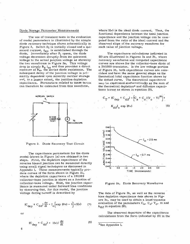
Diode Storage Parameter Measurements
The use of transient tests in the evaluation of model parameters is illustrated by the simple diode recovery technique shown schematically in Figure 2. Switch S1 is initially closed and a quiescent current, Iss• is established through the diode. Immediately after Sl opens, the diode voltage decreases abruptly from its quiescent voltage to the actual junc:tion voltage as shown by the two waveforms in Figure 3a. This voltage drop is simply Rs Iss and thus provides a direct measure of Rs, the series diode resistance. The subsequent decay of the junction voltage is primarily dependent upon minority carrier storage ?nrl. tn a lesser extent, the junCtion depletion capacitance. Paramet~rs related to these te1'lus can therefore be extracted from this waveform.
MERCURY SWITCH s,
r DIODE UNDER 'TEST. TO
OSCILLOSCOPE
. Figure 2. Diode Recovery Test Circuit
The capacitance parameters for the diode model (shown in Figure la) are obtained in two steps. First, the depletion capacitance of the reverse biased junction can be measured directly using small signal techniques as discussed in Appendix I. These measurements typically produce curves of the form shown in Figure 3c, where the deplet~on capacitance of a 2Nl989 collector-base junction is shown as a function of collector-base voltage. Ne'xt, the junction capacitance is measured under forward bias conditions by observing that, for this model, the junction voltage during turnoff .is described by
or
(8)
6
where·I(v) is the ideal diode current. Thus, the functional dependence between the total junction capacitance and the junction voltage can be computed from the ratio of the ideal current and the observed slope of the recovery waveform for each value of jUnction voltage.
The capacitance calculations indicated in (8) are illustrated in Figures 3a and 3b, where recovery waveforms and computed capacitance curves are shown for the collector-base diode of a 2Nl989 transistor. In the low voltage portion of Figure 3b, both capacitance curves are coincident and have the same general shape as the theoretical total capacitance function shown by the dotted curve. The theoretical capacita.nc:e way Lc C.lrprcoood m?.thPmAtir.ally as the sum of the theoretical depletion* and diffusion capacitance terms as shown in equation (9).
CT = (Cd + Cd_f) = rc + C /(V - V)mJ· + ep 1 L s . o .. o . . .
Kdi~o exp · (ev)
0.60
~ 0.58
g 0.56
0.54 w r., = 2.5 mo (!) 0.52 <(
~ 0.50 0 > 0.48
iS 0.46
1- 0.44 u ~0.42 ...,
0.40 0 0.5 1.0 1.5 2.0 2.5 3.0
Tl ME (microseconds l
Figure 3a. Diode Recovery Waveforms
The data of Figure 3b, as well as the reverse bias depletion capacitance data shown in Figure 3c, may be used to obtain a leasf-squares evaluation of the parameters Cs, C0 • V 0 , m and kdif in equation (9).
The observed departure of the capacitance calculations from the form indicated by (9) in the
*See Appendix I.
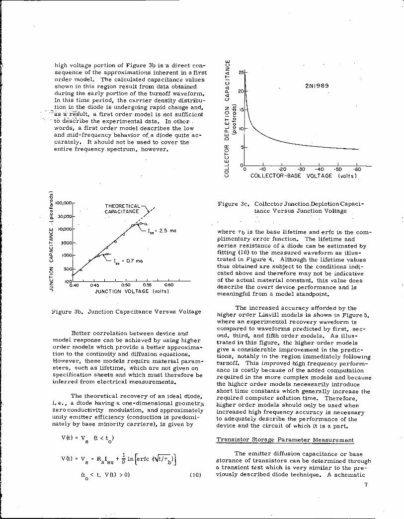
high voltage portion of Figure 3!:> is a direct consequence of the approximations inherent in a first order model. The calculated capacitance values shown in this region result from data obtained during the early portion of the turnoff waveform. In this time period, the carrier density distribution in the diode is undergoing rapid change and,
.::as ·a- result, a first order model is not sufficient · · tb des tribe the experimental data. In othe·r. .
words, a first order model describes the low and mid-frequency behavior of_a diode quite accurately. It should not be used to cover the entire frequency spectrum, however.
"' -o ~ 100,000 -0
·5. 30,000
w 10,000 u z <I 1- 3000 u <I Q_ <I u
z 0
1000
300
THEORETICAL' , CAPACITANCE ,\-"
,,'"
r •• = 2.5 mo
155
= 0. 7 mo
6 z ::J ....,
108L.4_0_L __ o~.4_5 __ L--i~o~.5~o--L-~o~.~=--L-=o~.s~o~--
JUNCTION VOLTAGE (volts)
Figure 3b. Junction Capacitance Versus Voltage
Better correlation between device and model response can be achieved by using higher order models which provide a qetter approximation to the continuity and diffusion equations. However, these models require material parameters, such as lifetime, which are not given on specification sheets and which must therefore be inferred from electrical measurements.
The theoretical recovery of an ideal diode, i.e .• a diode having a one-dimensional geometry. zero conductivity modulation, and approximately unity emitter efficiency (conduction is predominately by base minority carriers). is given by
v (t) = v (t < t ) s 0
(t < t. V(t) >0) 0
(10)
w (_)
z <( 25 I-
u 2N 1989 <( Q. 20 <( u
z~ ~ :: I- 0 w'Q _J .~ Q. c. w~
0
a:: 0 I-u w _J 0
-50 -60 _J 0 -10 -20 -30 -40 0
COLLECTOR-BASE VOLTAGE (volts). u
Figure 3c. Collector Junction Depletion Capacitarice Versus Junction Voltage.
where Tb is the base lifetime and erfc is the complimentary error function. The lifetime and series resistance of a diode can be estimated by fitting (10) to the measured waveform as illustrated in Figure 4. Although the lifetime values thus obtained are subject to the conditions indicated above and therefore may not be indicative of the actual material constant, this value does describe the overt device performance and is meaningful from a model standpoint •
The increased accuracy afforded by the higher order Linvill models is shown in Figure 5, where an experimental recovery waveform is compared to waveforms predicted by first, second, third, and fifth order models. As illustrated in this figure, the higher order models give a considerable improvement in the predictions, notably in the region immediately following turnoff. This improved high frequency performance is costly because of the added computation required in the more complex models and because the higher order models necessarily introduce short time constants which generally increase the required computer solution time. Therefore, higher order models should only be used when increased high frequency accuracy is necessary to adequately describe the performance of the device and the circuit of which it is a part.
Transistor Storage Parameter Measurement
The emitter diffusion capacitance or base storance of transistors can be determined through a transient test which is very similar to the previously described diode technique. A schematic
7
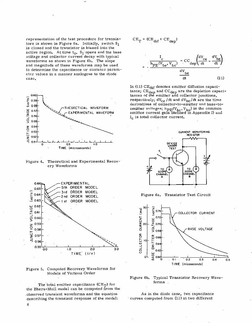
representation of the test procedure for transistors is shown in Figure 6a. Initially, switch S1 is closed and the transistor is biased into the active region. At time t 0 , s1 opens and the base voltage and collector current decay with typical waveforms as shown in Figure 6b. The slope and magnitude of these waveforms may be used to determine the capacitance or storance parameter values in a manner analogous to the diode case!
w 0.5 ',, /TIICOnCTICAL Wl\116:fORM
(!) ' ', EXPERIMENTAL WAVEFORM ~ 0.56 _J
0 0.55 > --.........._ z 0.54 0 ---...___ ·I-
0.53 u
0.52 z ::> ...., 0.51
0 0.5 1.0
TIME (microseconds-)
Figure 4. Theoretical and Experimental Recovery Waveforms
w 0.62 (!)
;:: 0.61. _j
0 0.60 > z 0.59
Q 0.58 1-u z ::::> --,
0.55 0.0
....-EXPERIMENTAL /~5th ORDER MODEL
/
ORDER MODEL ORDER MODEL ORDER MODEL
1.0 2.0
TIME. (tIT)
3.0
Figure 5. Computed Recovery Waveforms for Models of Various Order
The ·total emitter capacitance (CET) for the Ebers-Moll model can be computed from the
,observed transient waveforms and the equation d~scribing the transient response of the model:
8
Ic - CC (dVce - dVbe) hFE(Vbe' Vbc) dep · dt dt
dV · be
dt (11)
In (11) CEdif denotes emitter diffusion capaci-: tance; CEdep and CCdep are the depletion capacitances of the emitter and collector junctions, respectively; dV~e /dt and dVbe/dt are the tirne derivatives of collector-to-emitter a.nd base-toomitt9r vnlt:'lgPR; h!i'B(Vbe• Vb 0 ) is the common emitter current gain (defined in Appendix I) aud Ic is total collector current.
CURRENT MONITORING RESISTOR
TO SCOPE
CHANNEL B
+
Figure 6a. Transistor Test Circuit
~ 30 0
E COLLECTOR CUR RENT 1-z w 0.72 w (!)
BASE VOLTAGE
~ 20 ~ 0.70 ::> _J
u ~ 0.68 a: 0 ffi 0.66 1-u 10 1-w ~ 0.64 _J ::E _J w 0 0.62 u w
0.1 ' 0.2 0 ~ 0.
CD 0 0.3 0.4
TIME (micoseconds)
Figure 6b. Typical Transistor Recovery Waveforms
As in the diode case, two capacitance · curves computed from (11) at two different
0.5
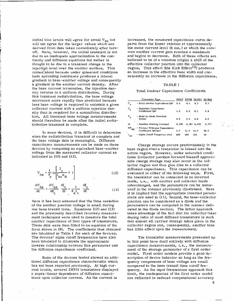
initial bias levels will agree for small Vbe but will not agree for the larger values which a-re derived from data taken immediately after turnoff. Here, however, the initial transient is not due to an inadequate approximation to the continuity and diffusion equations but rather is thought to be due to a transient change in the inject~gn level over the emitter surface, This comes~'.about because under quiescent conditions base spreading resistance produces a lateral gradient in base-emitter voltage and consequently a gradient in the emitter current density. After the base current terminates, the injection density returns to a uniform distribution, Durin~;
this transient redis.tribution, the base voltage decreases more rapidly than predicted because less base voltage is required to maintain a given collector current with a uniform injection density than is requir~d for a nonuniform distribution. All transient base voltage measurements should therefore be made after tqe initial redis-: tribution transient is complete,
In some devices, it is difficult to determine when the redistribution transient is complete and the base voltage data is meaningful, Diffusion capacitance measurements can be made on these devices by computing an equivalent base-emitter voltage from the measured collector current as indicated in (12) and (13),
(12)
(13)
Here it has been assumed that the time variation of the emitter junction voltage is small during one base transit time, Equations (12) and (13) and the previously described recovery measurement techniques were used to measure the total emitter capacitance of four types of transistors, These data were then fitted to an equation of the form shown in (9). The coefficients thus obtained are tabulated in Table I for each of the devices. The devices 1 alpha cutoff frequencies have also been tabulated to illustrate the approximate inverse relationship between this parameter and the diffusion capacitance coefficient.
Some of the devices tested showed an additional diffusion capacitance characteristic which has not been reported previously, At high current levels, several 2N9l8 transistors displayed a supra-linear dependence of diffusion capacitance upon collector current. As the current is
increased, the measured capacitance curve, departs from the linear relation at approximately the same current level (4 rna.) at which the common emitter current gain reaches a maximum and begins to decrease. Both of these effects are believed to be of a common origin; a shift of the effective collector junction into the c9llector region. This effect (the Kirk EffectlO) produces an increase in the effective base width and consequently an increase in the diffusion capacitance.
TABLE I
Total Emitter Capacitance Coefficients
Transistor :!Zee ~ ~2NI051~ c
s - Stray Header Capacitance (pf) 0. 4 0. 4 o. 3 o. 3
c 0
- Depletion Capacitance Coefficient (pf) I. 0 6. 3 8. I 5. 8
v 0
- Built-in Diode Potential (volts) o. 8 o. 8 o. 8 o. 8
- Junction Grading Constant 0. 390 o. 381 o. 400 o. 371
KEdif - Emitter Diffusion Capacitance Coefficient (pf/ma) 5. 2 11.0 40.0 9.0. 0
rae - Alpha Cutoff Frequency (me) 800 480 120 60
Charge storage occurs predominately in the· base region when a transistor is biased into the active region. However, under saturated conditions (collector junction forward biased) appreciable charge storage may also occur in the collector region and thus give rise to a collector diffusion capacitance. This capacitance can be evaluated in either of the following ways. First, the transistor can be connected in an inverted mode, i.e., with emitter and collector leads interchanged, and the parameters can be measured in the manner previously illustrated. Here it is implied that the appropriate inverted parameters are used in (11). Second, the base-collector junction can be considered as a diode and the parameters can be computed in the manner indicated in the diode section. The latter approach takes advantage of the fact that the collector-base doping ratio of most diffused transistors is such that almost all carrier storage takes place in the collector region and, consequently, emitter bias has little effect upon the measurement.
The transistor measurements presented up to this point have dealt entirely with diffusion capacitance measurements, i.e., the measurement of the storage parameter of a first order model. First order models provide a good description of device behavior so long as the frequency components of base voltage are small compared to the base transit time cutoff frequency. As the input frequencies approach this limit, the inadequacies of the first order model are reflected in reduced computational accuracy
9
and; therefore, one is forced to resort to higher order models.
High order Linvill models of the base re·gionrequire values for the base width and base lifetime. These values can be estimated as follows. u·nder quie-sc-ent or low frequency conditions, the minority carrier distribution in the base is nearly linear. Consequently, the base charge and collector or emitter curre!lt are approximately given by
Q = b
and
I e
(14)
( 15)
Solving (15) for Ze and substituting this result and the relationship between.le and Vbe into (14) gives
2 2 wb wb J
Q = -- I = -- I [exp (B V )-1 b 2D e 2D eo e be z z .
or
2 dQb wb
CEd.f = dV = 2D I B exp (B Vb ) 1 be , Z eo e e e
w2 b
= 2D B I = KEd .. I • Z e e 11e
Therefore,
w = b
(16)
The effective base width can thus be computed directly from B e• Dz and KEdif" .
10
The effective base lifetime can be estimated from the DC gain of the device ·and the base width by using the relation
or
KEdif 7 b = -0--. hFE •
e (17)
It should be emphasized that the lifetime determined by (17) may not be the actual material lifetime, since the gain of some devices is controlled by emitter efficiency or collector multiplication, terms which have been neglected in (.l'l). However, the incorporation of these effects into the lifetime term has little. effect on the high frequency accuracy of the model and-at the same time retains the proper bias dependence of DC current gain.
Permanent Damage Models
When semiconductor materials- are- exposed: to energetic· radiation,. some -of the. atoms of the · material are permanently displaced •. These dis:placements produ.ce ~hanges .in measurable device parameters such as gain, junction capacitance, series resistance, etc. Permanent damage in diodes and transistors can therefore be modeled by predicting or measuring the functional rela-:tions between the model parameters and the radiation flux.
Typical neutron induced changes of the Ebers-Moll model parameters are illustrated in Figure 7. In this figure, the average normal and inverted current gains (hFEN• hFEI), emitter and collector diode coefficients (leo• leo; Be, Be), and the emitter and collector diffusion capacitance coefficients of several 2Nl989 transistors are shown as a function of neutron flux. Data of the type shown in Figures 7a and 7b have- been well documented and, in fact, form the basis for much of the research concerning permanent damage mechanisms in devices. However, capacitance data, such as that shown in Figure 1c, have not been· published previously. -These data not only
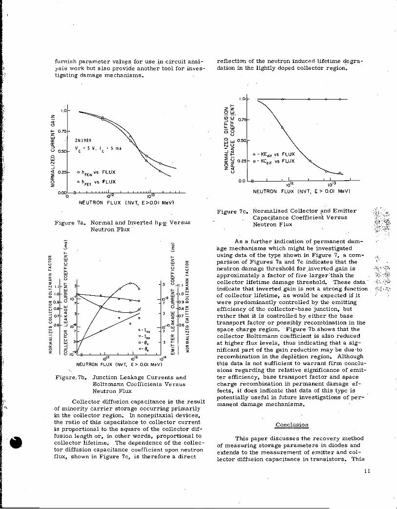
. ,
z :;x (!)
1-z w a: a: ::::> u 0 w N ::::i <(
:::!: a: 0 z
"' 0 I-u <( ..._ z z <(
:E N
~
furnish par~meter valu\=)S for use ~n circuit analysis work but also provide another tool for investigating damage mechanisms •
1.0
0.75
2N!989
0.50 v c 0 5 v. I c = 5 rna
0.25 0 hFEN VS FLUX
"' hFEI VS FLUX
0.00 101 0 10
NEUTRON FLUX (NVT, E>O.OI MeV)
Figure 7a. Normal and Inverted hFE Versus Neutron Flux
0 0 E E 1-z 1-w z u w "' 0
"- u I-
"- u w "- <(
0 "- ..._ u w
0 z 1-- 3 .u z
1.1 z 3 1.1 <(
w 1-- :E
0 1.0 a:: z 1.0~ a:: 10-9 ~ _co ::::> 0
~0.9 u 7 ~ 0.9 co
t; 0.8 u 0.8 e5 "" w I-
3 j 0.7 Cl 0.7 ~ <(
0 ~ u "" 0 0.6 10-10~ 0.60
"" N
.... <(
:E
"' 0 z
a:: o-leo 7 _J "" N 0 v-Ieo a:: .... 1--u w <(
w o-ec 3 1-- :E _J 1-- "' _J ,_e. ::;; 0 0 z u 10 w
1o'2 013 1o'4
NEUTRON FLUX (NVT, E > 0.01 MeV)
Figure .. 7b. Junction Leakage Currents and Boltzmann Coefficients Versus Neutron Flux
Collector diffusion capacitance is the result of minority carrier storage occurring primarily in the collector region. In nonepitaxial devices, the ratio of this capacitance to collector current is proportional to the square of the collector diffusion length or, in other words, proportional to collector lifetime. The dependence of the collector diffusion capacitance coefficient upon neutron flux, shown in Figure 7c, is therefore a direct
reflection of the neutron induced lifetime degradation in the lightly doped collector r~gion~
1-zz ow
1.0
3 ~ 0.75 LL."-LL.lt oo
u ~ w 0.50 NU -z ...J<( <(1-:::!:-a: ~ 0.25 oa. Z<(
u
"' - KEdil vs FLUX o - KCdil vs FLUX
0.0 Yl!---j__...:J__1.J.d"'2 __ _!_ _ __l__li0"713:;-----'-
NEUTRON FLUX (NVT, E > 0.01 MeV)
Figure 7c. Normalized Collector and Emitter Capac.itance Coefficieri"t Versus Neutron Flux
As a further indication of permanent damage mechanisms which might be investigated using data of the type shown in. Figure 7, a comparison of Figures 7a and 7c indicates 'that the neutron damage threshold for.inverted gain is approximately a factor of five larger'than the collector lifetime damage threshold. These data· indicate that inverted gain is not a strong function of collector lifetime, as would be expected if it were predominantly controlled by the emitting efficiency of the collector-base junction, but rather that it is controlled by either the base transport factor or possibly recombination in the space charge region. ·Figure 7b shows that the collector Boltzmann coefficient is also reduced at higher flux levels, thus indicating that a significant part of the gain reduction may be due ·to recombination in the .depletion region. Although this data is not sufficient to warrant firm conclusions regarding the relative significance of emitter efficiency, base transport factor and space charge recombination ih permanent damage effects, it does indicate that data of this type is potentially useful in future investigations of permanent damage mechanisms.
Conclusion
This paper discusses the recovery method of measuring storage parameters in diodes and extends to the measurement of emitter and collector diffusion capacitance in transistors. This
11
w·~.v:. ~A?~ ;j:.~ ' .. {~t· . ~~---~~.<:~~~:.
method has been used to characterize storage effects in devices having alpha cutoff frequencies in the range from 50 to 1000 megacycles. The relationship between these parameters and the distributed parameters required by the higher order. Linvill models is also considered.
Although emitter diffusion capacitance genP.rally has a strong influence on intrinsic transistor response, many circuit configurations arise where stray wiring capacitance and collector-base depletion capacitance are of equal or greater importance. For example, the Miller capacitance (the collector-base depletion capacitance amplified by the voltage gain of the circuit) of a 2N917 transistor operated in the common emitter mode (Ic = 1'. 0 rna, V c = 5 volts, .H.c = 1 UUU onm.s) is approximately 40 picofarads. This capacitance is large compared to the emitter diffusion capacitance <~ 5. 0 picofarads at Ie = 1. 0 rna) and therefore plays a dominate role in determining circuit response. Miller capacitance is also· increased by ·stray· wiring capacitance between the collector and base terminals. In the.·example cited above, as little as 3 picofarads of added wiring capa·citance would produce a threefold increase in the Miller capacitance and a corresponding reduction in high frequency performance of the circuit. It should therefore be clear that although the measurement of the detailed bias dependence.of model parameters is necessary for the efficient use, of .compute·r analysis. techni-.. ques, additiona1..paramete-rs, such,as.·stray · wiring. capacitance~· are· occasionaUy. of equal or-. greater importance in achieving·prediction·accuracy and must therefore be taken into account in modeling the complete circuit.
In addition to providing parameter data for circuit analysis work, the .measurement of storage parameters .in devices also provides a convenient tool for investigating the effects of neutron irradiation on some material parameters and for determining damage mechanisms in devices. The neutron degradation of minority carrier lifetime, for example, can be investigated by making diffusion capacitance measurements on a diode structure. The results of such measurements are illustrated in Figure 7c where the collector diffusion capacitance coefficient of a 2N1989 transistor is plotted versus. neutron flux. The presence of such mechanisms as Kirk Effect and the importance of these effects at various neutron exposures can also be investigated through the current dependence of diffusion capacitance •
. 12
Although the transient effects of ionizing radiation have not been treated explicity in this paper, two of the more important parameters required to predict these effects can be determined from the previously described measurements. First, the effective collector lifetime can be obtained by fitting equation (10) to the collector-base diode recovery waveform. Second, the effective base width can be determined from the coefficient relating diffusion capacitance to emitter current, as shown in equation (16).
Acknowledgment
The authors wish to thank Messrs. L. Horning anti C. Greer .fo1· llrt!li· as5i5le~.uo....c iil ubttti11il1g e.11d processing the data reported in this paper.
APPENDIX I
Common Parameters
Transistor current gain, the DC characteristics of the emitter-base and collector-base junctions and junction depletion capacitance are common to both the Ebers-Moll and ChargeControl models and therefore these parameters will be considered in this appepdix without particular reference to a specific device model. The functional relationship between these parameters and device bias levels is described in this appendix. Generally the form of these functional dependencies has been predicted from device theory; however, at extreme bias levels most devices depart from the theoretically predicted behavior. Therefore, a group of empirical formulas are presented which have been found to adequately describe device behavior over large bias ranges and which are useful in modeling transistors and diodes in computer circuit analysis programs.
Junction Characteristics
The DC characteristics of a junction can be represented by
(I. 1)
where I0 is the ideal leakage current, e is the Boltzmanu.term, r is a parameter which modifies the Boltzmann term to include space charge recombination, VB is the junction breakdown voltage and n and K are empirical constants which describe avalanche multiplication near breakdown. Since the last term in (I. 1) is small for forward bias conditions, Io and e I r may be evaluated from a graph of ln (I) versus V for positive V. Similarly, constants K and n can be determined from a plot of ln (I) versus ln (IV/VB I) for V approaching -VB
Equation (I. 1) ignores several effects which can be significant in some situations. First, it is assumed that series bulk resistance is modeled by lumped parameter components appearing
· elsewhere in the model. Conductivity modulation at high currents must also be taken into account in these lumped components. Second,
the breakdown behavior described in (I. 1) only describes an. avalanche type breakdown. Surface breakdown effects are not included in this equation.
Transistor Current Gain Expressions
The large signal current gain of a normally ·biased transistor is usually stated in terms of the common base (aN) or common emitter (hFEN) transfer ratios. These parameters (as well as their inverted counterparts £l'I and hFEI) are dependent upon bias and consequently the analytical form of this dependence should be included in the device model. Since the inverted parameters have little effect upon model accuracy, they can generally be assumed to be independent of bias and therefore they will not be considered in the · following discussion. Furthermore, only the form of hFEN is considered in detail since aN can .be easily computed from hFEN data.
For most diffused transistors operated at low current levels, the current dependence of the current gain (hFEN) is controlled by recombination in the emitter space charge region. Under these conditions, the gain can be approximated by
· .. ··~_;. ~ . :t ... · · . . . . ~: . _.: t~.:
' : ,., : .• ;~
(I. 2) ·.~- :!: ;·;;;:
where eh is normally less than q/kT. At intermediate current levels, either recombination in the base region or emitter efficiency may limit the continuing increase of hFEN with current that is predicted by (I. 3). This additional effect can be modeled by modifying (I. 2) by the constant term hFE1• as shown in (I. 3).
hFElhFEO exp (eh Vb ) h (V ) = e · (I. 3)
FEN be hFEl + hFEO exp (eh Vbe)
At very high current levels, two additional effects tend to decrease the gain. First, if the injection level is sufficiently high, conductivity modulation occurs in the base region and causes a decrease in emitter efficiency and base transport factor. This effect is compounded by the base current generated transverse emitter voltage gradient which increases the injection level at the emitter periphery. Second, the high carrier _densities in the base cause the apparent collector junction to shift into the collector region thereby increasing the effective base width and decr'easing the
13
. '~.

current gain. Relating these last two effects to device structure is very; complicated and cannot generally be done with great accuracy. The following modification of (I~ 3), which attempts to describe these effects. is .entirely empirical and the parameters of this equation are subject to large unit-to-unit variations.
The variations of hFEN with collector-base voltage is primarily caused by the Early EffectS and avalanche multiplication in the collector depletion region. Although these mechanisms are conceptually different, both can be represented either in terms of a collector multiplication factor, me (Vbc>• or in terms of a voltage· dependent current gain. This paper considers the former approach .and. assumes that both, effects. are described in. terms of a.leakage current whose magnitude is proportional to. rile (Vbc> times the collector current. Under this assumption,. the current-'voltage relations for the emitter.and. collector junctions may be written as
Icf =leo [exp (ecvbc) -1] -Icmc(Vbc)
Ief= leo [exp (eevbe) -1] -Ieme(Vbe)
Under normal bias conditions (V be< 0 and V. "" 0. 7), (I. 5) reduces to
be
I ""-I m (V ) cf c c be
I "" I "" I [exp (8 Vb ) -1] ef e eo e e
(I. 5)
since me(Vbe) is very small for small _voltages. and I is negligible. Furthermore, smce Icf 1s a lea~~ge current under these bias conditions it will always be oriented in opposition to the normal base current; therefore, the total effective base current will be the difference between the external base current, Ib and Icf· Therefore,
1c = -hFEN(Vbe) ~b + 1cf] -hFEN(Vbe)
~b- 1cmc(Vbc>] (I. 6)
14
or, solving for Ic•
(I. 7)
Equation (I. 7) shows that the effective current gain becomes infinite whenever mc(Vbc> approaches 1/hFEN (Vbe>· Therefore, the open base breakdown voltage (BV CEO) is always less than the collector jun:ction breakdown potential (BV CEO) since colle~tor ~reakdown doe~ not occur until mc(Vbc> 1s umty.
The measurement of hFEN(Vbe> and m (Vb ) is facilitated by (I. 6). By varying Vbc a~d Ib csuch that Ic is constant, the mu~tiplication factor mc(Vbc> ~an be measured d1rectly.
'In Figure I. 1, a fam1ly of Ib versus V cb curves are shown for several collector current levels, each cuvve~·having been normalized· by dividing· by the appropriate collector: current. The func.tion mc(Vbc) is determined by subtracting any of the curves.fr.om the extrapolated .ordinate intercept for that curve. The values ·for 1/hFEN(Vb ) are determined by extrapolating each curve lo zero collector volts and using the relation
1 V "=' - ln(I /a I )
be e c N eo e
to determine the corresponding value· of Vbe· These operations yield the hFEN(Vbe) and mc(Vbc> curves 'shown in Figures I.2a and I. 2b.
0 i= 0.04 <( 0:
1-z w 0.03 -0: 0: :::> u 0: 0.02 0 1-u w .J 6 0.01 u w ({) <( (]) 0.00
2NI051
10 20 30 40 50 60
COLLECTOR VOLTAGE (volts)
Figure I. 1. Base-Collector Current Ratio Versus Collector Voltage for Fixed Collector Current

60
z I.U ...
.r.
z <I (!)
1-z w a:: a:: ::J (.)
0.66 0.68 0.70 0.72 0.74 0.76 0.78 0.80 BA$E-EMITTER VOLTAGE (volts)
FigUre I. 2a. Current Gain Versus Base-Emitter Voltage
0:: 0 f(.)
~ 0.04
z 0 f<l (.) 0.02 ....J a..
~ ::> ~ o.oo~--L---L-~~~L_~--~----
o 10 20 30 40 50 60 COLLECTOR VOLTAGE (volts)
Figure I. 2b. Collector Multiplication Ratio Versus Collector ·voltage
Transistor DC Characteristics
The DC characteristics of a transistor are described by two equations4 which relate total emitter and collector currents to junction currents and gain coefficients
(I. 8)
where·ai is assumed to be constant,
(I. 9)
and Ief and Icf are given by (I. 5). Since Ief and Icf are in .turn functions of Ie and Ic• (I. 8) is an implicit function of Ie and Ic which cim be solved explicitly to obtain ·
.\·'
where
I'f =I fexp (8 Vb )-11 c eo L e c j
I If = I [exp (8 vb )-11 • e co · e e J
Note that all terms in (I. 10) are expressed as functions of the junction voltages Vbe and Vbc -this feature is requi:J;'ed for efficient numerical solution of the models and circuit transient behavior.
Depletion Capacitance
In addition to the DC parameters discussed above, the three models under consideration also include depletion capacitance, i.e., the capacitance associate.d with the space charge found in junction transition regions. This capacitance can be measured with a standard capacitance bridge as long as the junction is not conducting an appreci- · able cu.rrent. Depletion capacitance cannot be measured in the forward conduction region because of the effects of minority carrier storage (diffusion capacitance) and the previously described resistance and temperature effects.
The relationship between the theoretical depletion capacitance and junction voltage is, in general, very complex and cannot be expressed
15
:'.;;:~· :·:<~!
',:~;,,; :~ ·. ~1¥
in closed form. However, an approximate expression, given in (I. 11), has been derived which is reasonably valid for reverse-biased junctions,
cd (V) ;: c + c I (V - V)m ep s o o (I. 11)
This expression has been found to fit abrupt junctions, e. g., the emitter junction of a diffused transistor, quite well(- ±lo/o). However, junctions which ·have a smaller doping gradient, such as the collector junction of a h~gh voltage transistor,
do not usually follow this expression and errors of ±15o/n are frequently em:uuntered. Furthermore, this expression should be used with caution when extrapolating into the forWlll'd bia~:> region because of the pole that exists at V = V
0•
Certainly V0 should never be less than the maximum voltage obtained in the particular application.
The approximate value for the coefficient Cs of (I. 11) can be obtained by direct measurement on a device which has been electrically opencircuited and the remaining coefficients can be obtained from a plot of ln (Cdep(V)-Cs) versus ln (V 0 - V). Successive plots are made with different V 0 values until a straight line is obtained on log-log graph paper. The appropriate V 0 value is that value which produces the best straight line. Once the proper V 0 value is obtained, the value of n and C0 is given by the slope and intercept, respectively, of the straight-line log-log plot.
A c
dep
cdif
CT
CEdif
ccd ep
Definition of Symbols
Junction area , diode depletion capacitance
diode diffusion capacitance
total diode capacitance
emitter junction diffusion capacitance
emitter junction depietion capacitance
collector junction depletion capacitance
total emitter junction capacitance
stray wiring and device header capacitance
proportionality constants
diffusion constant for charge carrier z
Inverted common emitter current gain
-hFEO
hFEl
hFEN(Vbe)
common emitter gain coefficient
common emitter gain coefficient
common emitter DC current gain for v cb = 0
hFEN(Vb , Vb ) common emitter DC current gain e c as function of Vbe and Vbc
1 0
I c
I e
~ I ss
Iz
IA
IB
Jz I
K,~,K 1,K2 Kdif
KEdif
KCdif
me (Vbc)
m
n
N e
N c
r
R s
s
v 0
total emitter diode current
total collector diode current
emitter junction saturation current
collecto._r junction saturation current
diode satu!·ation current
tot:;\l d<avirP. rnllP.r.tnr ~urrent
total device emitter current
total device base current
steady state diode current
current carried by carrier Z
current entering boundary A.
current entering boundary B
current density for charge carrier Z
proportionality constants
diffusion capacitance proportionality constant
emitter diffusion capacitance proportionality constant
collector diffusion capacitance proportionality constant
collector multiplication factor
junction grading constant
junction breakdown coefficient
emitter diode Boltzmann modification term
collector diode Boltzmann modification term
electronic charge
total minority carrier charge stored in the base region
total minority carrier charge stored between surfaces A and B
diode Boltzmann term modification parameter
bulk series resistance of diode
gain coefficient
diode built-in potential
steady state diode voltage
junction breakdown voltage
base-emitter voltage
collector-emitter voltage
width of base region
minority carrier density for arbitrary carrier Z at surface A
minority carrier density for arbitrary carrier Z at surface B
minority carrier density for arbitrary carrier Z at surface K ·
z 0
equilibrium minority carrier density for arbitrary carrier Z
T
equilibrium minority carrier density for arbitrary carrier Z at b<!-Seemitter junction
emitter junction injection density
normal DC common .base current gain
inverted DC common base current gain
Boltzmann factor (q/kT)
Boltzmann term for emitter junction
Boltzmann term for collector junction
modified Boltzmann gain coefficient
modified Boltzmann gain coefficient
carrier mobility of carrier Z
minority carrier lifetime in the base region
minority carrier lifetime
References
1. Air Force Weapons Laboratory Technical Documentary Report, 11Automatic Digital Computer Program for Determining Responses of Electronic Systems to Transient Nuclear Radiation, 11 WL-TDR-64-62, Supplement II (Kirtland Air Force Base, Albuquerque, New Mexico) May 1964.
2. A. F. Malmberg and F. L. Cornwell, 11 NET-1 Network Analysis Program, 11 LA-2853 (Los Alamos Scientific Laboratory, Los Alamos, New Mexico) April 30, 1963.
3. R. Reid, "A System Analysis Program, Technical Report No. 1, 11 Division of Engineering. Research, Michigan State University, August 1962.
4. J. J. Ebers and J. L. Moll, "Large Signal Behavior of Junction Transistors," Proc. I. R. E., Vol. 42, N. 12, December 1954, pp. 1761-72.
5. R. Beaufoy and J. J. Sparks, "The Junction Transistor as a Charge-controlled Device, 11
A. T. E. Journal, Vol. 13, N. 4, October 1957, pp. 510-527.
6. J. G. Linvill, "Lumped Models of Transistors and Diodes, 0 Proc. I. R. E., Vol. 46, N. 6, June 1958, p. 949.
7. D. J. Hamilton, F. A. Lindholm, and J. A. Narud, "Large Signal Models of Junction Transistors," I. S. S.C. C. Digest, February 1963, pp. 56-57.
8. A. B. Phillips, Transistor Engineering, McGraw-Hill Book Co., Inc., 1962.
9. R. L. Pritchard, 11Electric-Network Representation of Transistors - A Survey, 11
I. R. E. Trans. - Ckt. Theory, March 1956.
10. C. T. Kirk, 11A Theory of Transistor Cutoff Frequency Falloff at High Current Densities, 11 I. R. E. Trans. - Elec. Dev., (March 1962 ).
17
.;.
) : ~:· . ;~: '.;',· ' ;
·.:
.:· l :~
l fi~ ' ~·
'~I ,.