Embed Size (px)
Citation preview

MIC2555
USB – OTG Transceiver
MLF and MicroLead Frame are registered trademarks of Amkor Technology, Inc. Micrel Inc. • 2180 Fortune Drive • San Jose, CA 95131 • USA • tel +1 (408) 944-0800 • fax + 1 (408) 474-1000 • http://www.micrel.com
December 2006 M9999-121406
General Description MIC2555 is a USB On-The-Go (OTG) transceiver designed to enable intelligent self-powered devices to communicate on a peer-to-peer basis with other USB and USB OTG enabled devices. Designed to perform as a PHY for USB Serial Interface Engines (SIE), MIC2555 is compatible with a wide variety of stand-alone OTG SIE chips, OTG IP cores (used in ASIC and COT designs), and Application Specific Standard Products (ASSPs). MIC2555 is fully compliant to USB-IF’s Universal Serial Bus Specification 2.0 and the On-The-Go Supplement Rev 1.0a, for Low speed and Full speed operation, and allows dual-role device (DRD) operation via an I2C based controller interface. The controller’s robust register set permits full control over bus and interface activity for transacting Session Request Protocol (SRP) and Host Negation Protocol (HNP) sequences. Messaging between Host and Target devices can utilize either USB or UART signaling methods. Additionally, the MIC2555 permits audio signaling on its D+, D- and ID lines in support of analog car kit applications. USB communication is complemented with on-chip D+, D- pull-up/pull-down resistors, an integrated charge pump and low dropout voltage regulators to provide stable internal supply voltages and to supply VBUS power when operating as an A-device. Logic input levels spanning 1.6V to 4.5V ensure compatibility with current and future generations of process technology. The MIC2555 is offered in a space saving 4mm x 4mm 24-pin MLF® package. Data sheets and support documentation can be found on Micrel’s web site at www.micrel.com.
Features
• Complies with USB-IF USB standard 2.0 and OTG supplement Revision 1.0a.
• Provides signaling and control logic for SRP and HNP, enabling USB Dual-role device operation.
• Designed for Full-speed and Low-speed USB communications.
• I2C controller interface. • Offers 3 modes of operation: • USB • UART • Audio • Operates with VLOGIC of 1.6V – 4.5V, assuring
compatibility with low voltage ASICs. • Tri-level ID detection for recognition of USB and non-
USB devices. • Supports USB /Car Kit audio interface. • Allows Single-ended and Differential Logic I/O. • Integrated charge pump for VBUS supply. • On-chip pull-up, pull-down resistors minimize external
component count. • Suspend and Power-down modes for power
conservation. • Operates over the full Industrial Temperature range: –
40°C to +85°C. Applications • Cellular Telephones • PDAs • Digital Still Cameras • Camcorders • Data Cradles • CD and MP3 players • Printers

Micrel, Inc. MIC2555
December 2006 2 M9999-121406
Ordering Information
Part Number Standard Pb-Free
Address Junction Temp. Range Package
MIC2555-0BML MIC2555-0YML 0x –40°C to +85°C 24-pin MLF® MIC2555-1BML MIC2555-1YML 1x –40°C to +85°C 24-pin MLF®
Typical Application
VBATVDD
VDD_LOGIC
OE_INT/
VTRM
VBUS
RS
RS
4.7µF
GND
D–
D+USBPort
VBUS
IDRCV
DAT_VP_RX
SE0_VM_TX
D+
D–
SCL
SDA
GND
MIC2555USB SIEController
VCC
SystemSupply Voltage
CAP++
CAP+CAP-
0.22µF
220µF
10µF
MIC2555 Typical Application Circuit
Pin Configuration
RCVSE0_VM_TXDAT_VP_RX
OE_INT/INT/
GPIO_0_RX
VTRMVBUSD-D+IDGND_D
CA
P+
VB
ATC
AP
-G
ND
_AV
DD
_LG
C
CA
P++
RE
SE
T/A
DR
0S
DA
SC
LG
PIO
_1_T
X
GP
IO_2
4mm × 4mm 24-pin MLF (ML)

Micrel, Inc. MIC2555
December 2006 3 M9999-121406
Pin Description Pin Number Type Pin Name Pin Description
1 O RCV Output from differential receiver.
2 I/O SE0_VM_TX
= SE0 in USB DAT-SE0 mode = VM in VP-VM mode. = UART Transmit output when in UART Mode See figures 1 and 2 on page 4
3 I/O DAT_VP_RX
= DAT in USB DAT-SE0 mode. = VP in VP-VM mode = UART Receive input when in UART mode See figures 1 and 2 on page 4
4 I/O OE_INT/
A Multi-mode pin controlling various functions in conjunction with control register bits. A logic LOW on this pin gives the following results: = OE (Output Enable): Enables D+, D- as USB outputs. = INT/ (Interrupt): Active LOW output when register bits ‘suspend’ and ‘oe_int_en’ both = 1.
5 O INT/ Interrupt (bar). Open Drain Active LOW output. May be wire-ORed with other interrupt signals.
6 I/O GPIO_0_RX = General purpose I/O. Open drain output. = Alternate UART Receive input. See figures 1 and 2 on page 4
7 I/O GPIO_1_TX = General purpose I/O. Open drain output. = Alternate UART Transmit output. See figures 1 and 2 on page 4
8 I/O SCL I2C Clock 9 I/O SDA I2C Data
10 I ADR_0 Sets Address bit A0 of I2C controller. This pin is a digital input and must not be left floating.
11 I RESET/ System reset. Active LOW. 12 I/O GPIO_2 General purpose I/O. Open drain output. 13 I/O GND_D System Digital ground.
14 I/O ID Identification input. Monitors the ID pin of the USB connector and indicates both the presence of a device and type (USB or not USB).
15 I/O D+
= USB D+ when in USB mode. = UART Receive in UART mode. = Right Speaker audio output in stereo mode. = Microphone signal from Car Kit.
16 I/O D-
= USB D- when in USB mode. = UART Transmit out in UART mode. = Left Speaker audio output in stereo mode. = Monaural audio output to Car Kit.
17 I/O VBUS USB 5V power. 18 I/O VTRM Internal 3.3V supply. Sets USB signal levels. 19 I CAP++ Positive lead for charge pump reservoir capacitor. 20 I CAP+ Positive lead for charge pump capacitor.
21 I VBAT Positive voltage from battery. Supplies power to MIC2555 internal circuitry and power for charge pump when driving VBUS.
22 I CAP- Negative lead for charge pump capacitor. 23 I GND_A Analog ground. Isolated Charge Pump ground.
24 I VDD_LGC Logic supply voltage. Used to set logic levels between MIC2555 and System Controller / ASIC.

Micrel, Inc. MIC2555
December 2006 4 M9999-121406
Interconnect Diagrams
SE0_VM_TX
DAT_VP_RX
D+
D–
MIC2555
Host Controller 1
UART
UART
SIEI2C
TX
RX2:1
Figure 1. Controller with Multiplexed Serial Interfaces
SE0_VM_TX
DAT_VP_RX
D+
D–
MIC2555
GPIO_0_RX
GPIO_1_TX
UART
UART
SIEI2C
Host Controller 1
TX
RX
Figure 2. Controller with Parallel Serial Interfaces
NOTE 1 Examples of Host Controller are:
• Baseband Processor/IC • µProcessor • Modem

Micrel, Inc. MIC2555
December 2006 5 M9999-121406
Absolute Maximum Ratings(1)
Power Supply Voltage: VBAT, GPIO- ................................................. -0.3V to +6.0V
VDD_LGC ......................................... –0.3V to +6.0V and ≤ VBAT USB Bus Voltage VBUS ......................................................................–0.3V to +6.0V VDD_LGC .........................................–0.3V to +6.0V and ≤ VBUS Voltage On Any Other Pin............................ –0.3V to +4.5V Current Into/Out of Any Pin .......................................±10mA Junction Temperature ................................................ 150°C Storage Temperature .................................–65°C to +150°C ESD Ratings:..............................................VBUS, D+, D–, ID Human Body Model ..............................................15 kV ESD Ratings:................................................... All other pins Human Body Model ................................................2 kV
Operating Ratings(2)
Power Supply Voltage: VBUS.......................................................... 4.4V to 5.25V VBAT............................................................ 3.0V to 4.5V Operating Temperature................................ –40°C to +85°C Package Thermal Resistance .................................. 49°C/W
Electrical Characteristics(3)
Test condition is 25°C unless otherwise specified. Bold indicates -40°C + 85°C, VBAT = 3.6V, VDD_LGC = 3.6V, VBUS = 5.0V, VTRM = 1µF, C+ = 0.22µF, C++ = 220µF, CVBUS = 10µF
Symbol Parameter Condition Min Typ Max Units Power Supplies VBAT System Supply Voltage 3.0 4.5 V VDD_LGC Logic Supply Voltage 1.6 VBAT V
VTRM Termination Voltage (internal supply voltage) ITRM ≤ 2.5mA, 3.0 < VBAT < 3.6V 2.8 3.3 3.6 V
IBAT_PD System Supply Current Power Down mode 13 20 µA IBAT_SUS System Supply Current Suspend mode 140 250 µA
IBAT_FS_I System Supply Current Full Speed, Idle, D+ ≥ 2.8V, D- ≤ 0.3V, IVBUS = 0mA 2.8 5.0 mA
IBAT_FS_HC System Supply Current Full Speed Transmitting 12Mb/s, CLOAD ≤ 350pF on D+, D-, IVBUS = 0mA 17 40 mA
IBAT_FS_LC System Supply Current Full Speed Transmitting 12Mb/s, CL = 50pF on D+,D-, IVBUS = 0mA 2.5 6 mA
IBAT_LS_HC System Supply Current Low Speed Transmitting 1.5Mb/s, CL = 350pF on D+,D-, IVBUS = 0mA 6.5 12 mA
IVBUS_S Current drawn by System from VBUS Suspend mode, OE_INT/ = 1 80 100 µA
IVDD_LGC Current drawn by System for core logic OE_INT/ = 1 7 15 µA
Charge Pump and VBUS VBUS_ OUT Voltage Output to VBUS IBUS = 10mA, VBAT = 3.0V 4.4 5.0 5.25 V IVBUS VBUS Output Current 4.4V ≤ VBUS ≤ 5.25V 10 27 mA
RVBUS_PU B device SRP Pull-up Resistor on VBUS Pull-up voltage = VTRM 281 1300 7500 Ω
RVBUS_PD B device SRP Pull-down Resistor on VBUS Pull-down to GND 675 2300 7500 Ω

Micrel, Inc. MIC2555
December 2006 6 M9999-121406
Symbol Parameter Condition Min Typ Max Units RA_BUS_IN VBUS Input Resistance Seen from VBUS pin to GND 40 63 100 kΩ
VTH_VBUS ‘VBUS Valid’ Comparator Threshold Voltage 4.4 4.5 4.6 V
VTH_SV “Session Valid’ Comparator Threshold Voltage 0.8 1.4 2.0 V
VTH_SE “Session End’ Comparator Threshold Voltage 0.2 0.4 0.8 V
ID
VTHH_R_ID Upper Threshold for ID Resistor Sensing VBAT = 3.0V 2.45 2.55 2.65 V
VTHL_R_ID Lower Threshold for ID Resistor Sensing VBAT = 3.0V 0.35 0.42 0.55 V
RID_PU Pull-up Resistor switched to ID for detecting non-USB devices
70 90 130 kΩ
IID_WPU Weak Pull-up current source driving ID pin VID = 0V 2 4 6 µA
RID_SW_GND Interrupt Pulse Switch VID ≤ 200mV
1.0 4.0 kΩ
Logic Levels - SDA, SCL, ADR0, OE_INT/, SE0_VM_TX, DAT_VP_RX, RCV, INT/, RESET/ & GPIO
VIL LOW-Level Input Voltage 0.3x VDD_LGC
V
VIH HIGH-Level Input Voltage 0.7x VDD_LGC
V
Input Hysteresis
SDA, SCL
100 mV
VIL LOW-Level Input Voltage 0.15x VDD_LGC
V
VIH HIGH-Level Input Voltage
ADR0, OE_INT/, SE0_VM_TX, DAT_VP_RX, RCV, INT/, RESET/ & GPIO Applies to USB and UART modes. 0.85x
VDD_LGC V
IIN_LGC Input Leakage Current 1.6V ≤ VDD_LGC ≤ 4.5V -5 +5 µA VOL LOW-Level Output Voltage IOL = 100µA .02 0.1 V
VOH HIGH-Level Output Voltage IOH = 100µA 0.9x VDD_LGC V
VOL_SDA LOW-Level Output Voltage at SDA pin IOL = 5mA 0.3x
VDD_LGC V
VOH_SDA HIGH-Level Output Voltage at SDA pin RSDA_PU = 3.0K 0.7x
VDD_LGC V
VOL_GPIO LOW-Level Output Voltage at GPIO pins IOL = 10mA 150 250 mV
VOH_GPIO HIGH-Level Output Voltage at GPIO pins RPU = 3.0K VDD_PU –
0.1V VDD_PU V
IOH_GPIO GPIO Output driver leakage current VDD_PU = VOH_GPIO = 5V 1 30 µA

Micrel, Inc. MIC2555
December 2006 7 M9999-121406
Symbol Parameter Condition Min Typ Max Units Transceiver DC Characteristics - D+, D- VDI Differential Input Sensitivity |(D+) – (D-)|, VIN = 0.8V – 2.5V 0.2 V
VCM Differential Common-Mode Range Includes VDI Range 0.8 2.5 V
VTH_SE Single-Ended Receiver Threshold 0.8 1.5 2.0 V
VHYS Receiver Hysteresis D+, D- 200 mV VOL LOW-Level Output Voltage OE_INT/ = 0, RL = 1.5kΩ to 3.6V 0.1 0.3 V VOH HIGH-Level Output Voltage OE_INT/ = 0, ISOURCE = 1mA 2.8 3.3 3.6 V
RDRV Transceiver Output Resistance D+, D- 5 12 24 Ω
Active 1.425 2.25 3.09 kΩ RPU_D Internal Pull-Up Resistor on
D+ and D- VTRM to D+ or D- Idle 0.900 1.24 1.575 kΩ
RPD_D Internal Pull-Down Resistor or D+ and D- D+ to GND, D- to GND 14.3 19.5 24.8 kΩ
CIN_D Transceiver Input Capacitance
D+, D- pins to GND See Note 4 20 pF
VTHL_INT_HI Interrupt Detector Threshold HIGH 2.5 3.0 3.3 V
VTHL_INT_LO Interrupt Detector Threshold LOW 0.3 0.5 0.7 V
Transceiver AC Characteristics - D+, D-
VC2C
Channel-to-Channel Isolation between D+, D- and ID pins (in audio mode)
DC bias (pin to GND) = 0.4V AC signal = 600mVp-p Freq. = 2kHz See Note 4
-60 dB
ZOUT_3S_D High-Z State Output Impedance
0V < VD < 3.6V, f = 2kHz OE_INT/ = 1 Measured at D+, D- pins, with respect to GND See Note 4
300 kΩ
Data Rate FI2C I2C signaling rate VBAT = 3.6V 100 400 kbps VBAT = 3.0V 100 200 kbps Driver Characteristics - Full Speed TAMB = 25°C tR_FS
tF_FS
Transition Time: Rise Time Fall Time
CL = 50pF to 125pF See Note 4
4 4
12.5 12.5
20 20
ns ns
tR / tF Rise/Fall Time Matching (TR/ TF) 90 111.11 %
VCRS Output Signal Crossover Voltage 1.3 2.0 V
tPLH tPHL
Propagation delay LOW to HIGH HIGH to LOW See Note 4
18 18
ns ns
Micrel, Inc. MIC2555
December 2006 8 M9999-121406
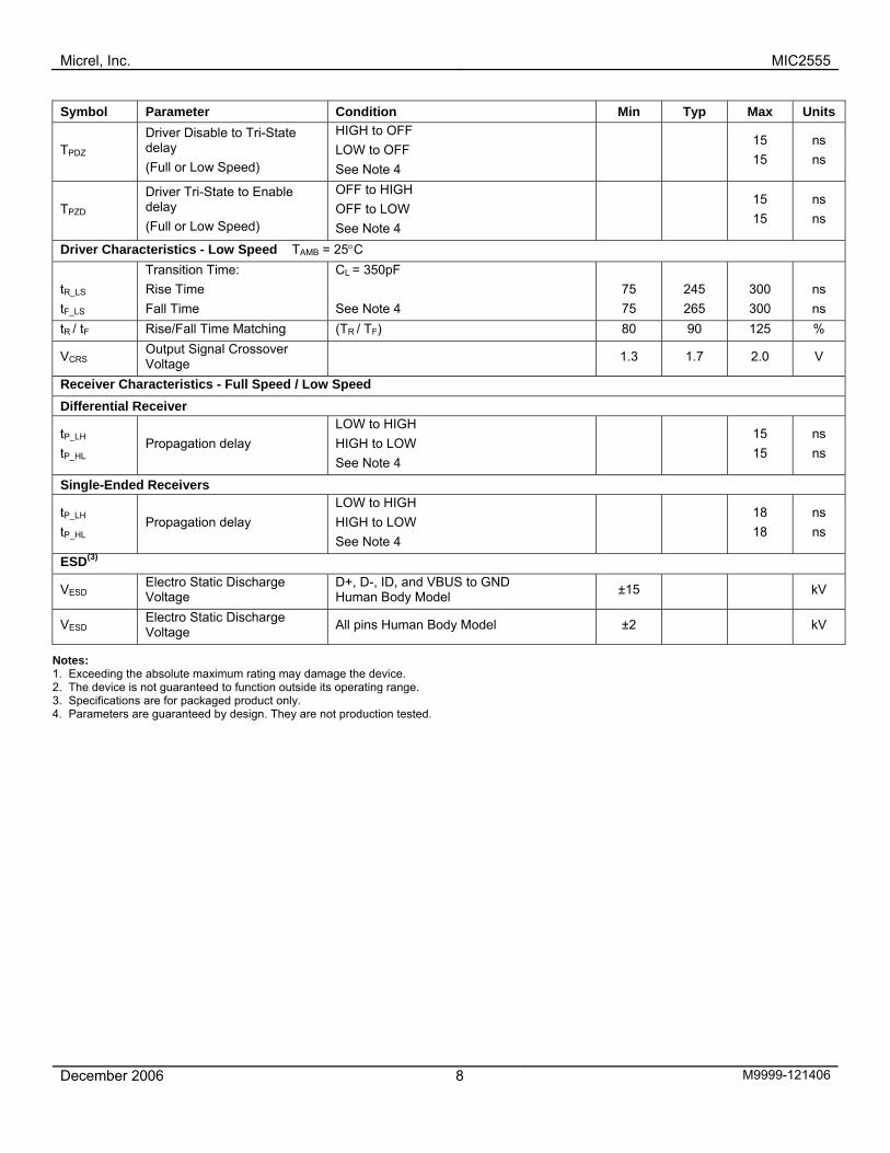
Symbol Parameter Condition Min Typ Max Units
TPDZ Driver Disable to Tri-State delay (Full or Low Speed)
HIGH to OFF LOW to OFF See Note 4
15 15
ns ns
TPZD Driver Tri-State to Enable delay (Full or Low Speed)
OFF to HIGH OFF to LOW See Note 4
15 15
ns ns
Driver Characteristics - Low Speed TAMB = 25°C tR_LS
tF_LS
Transition Time: Rise Time Fall Time
CL = 350pF See Note 4
75 75
245 265
300 300
ns ns
tR / tF Rise/Fall Time Matching (TR / TF) 80 90 125 %
VCRS Output Signal Crossover Voltage 1.3 1.7 2.0 V
Receiver Characteristics - Full Speed / Low Speed Differential Receiver
tP_LH tP_HL
Propagation delay LOW to HIGH HIGH to LOW See Note 4
15 15
ns ns
Single-Ended Receivers
tP_LH tP_HL
Propagation delay LOW to HIGH HIGH to LOW See Note 4
18 18
ns ns
ESD(3)
VESD Electro Static Discharge Voltage
D+, D-, ID, and VBUS to GND Human Body Model ±15 kV
VESD Electro Static Discharge Voltage All pins Human Body Model ±2 kV
Notes: 1. Exceeding the absolute maximum rating may damage the device. 2. The device is not guaranteed to function outside its operating range. 3. Specifications are for packaged product only. 4. Parameters are guaranteed by design. They are not production tested.

Micrel, Inc. MIC2555
December 2006 9 M9999-121406
Functional Diagram
SerialController
VTRM
VTRM
VBAT
VDD_LGC
INT/
SDA
SCL
RESET/
ADR_0
GPIO_1_TX
GPIO_0_RX
DAT_VP_RX
SE0_VM_TX
OE_INT/
RCV
C- C+ C++
VBUSComparator
ID Detector
InterruptDetector
Pull-Up/DownResistors
GND_D
GND_A
D-
D+
ID
VBUS
Pull-Up/DownResistors
MUX
Voltage Doubler and5V Regulator
TXD
DiffTX
RXD
SE
SED-
DiffRX
GPIO_2
D+
MIC2555 Block Diagram
Micrel, Inc. MIC2555
December 2006 10 M9999-121406
Functional Description The MIC2555 is designed to provide full USB On-The-Go (OTG) connectivity in mobile systems where low power and small size are key considerations. Intended for use in self-powered systems, the MIC2555 draws no current from VBUS for its operation, but will supply a minimum of 10mA at 5V to VBUS, from an on-chip charge pump, when operating as an A-device. The MIC2555 meets USB physical layer specifications while operating with logic supply voltages as low as 1.6V and battery voltages down to 3.0V. MIC2555 operation is controlled through an I2C bus by reading and/or writing to registers within the MIC2555. Control registers are used to set the operational mode to USB, Audio or UART (‘RS232’ format). Other features include VBUS comparators for SRP detection and ID pin recognition of USB and non-USB peripherals. The MIC2555 minimizes collateral components, requiring only 4 external capacitors and two resistors. All USB required pull-up/pull-down resistors are on-chip. 15KV ESD protection on all pins exposed to user contact (VBUS, D+, D-, ID and GND) eliminates the need for external ESD transient protection devices. Definitions and Conventions
Car Kit = A non-USB target device I2C = Inter IC Bus (I2C) NUT = non-USB target device OTG(1) = On-The-Go SIE = Serial Interface Engine
SE0 = Single Ended Zero
SRP = Session Request Protocol
USB = Universal Serial Bus
USB-IF = USB Implementers Forum
Serial Controller = Means the I2C control function within
MIC2555. UPPER CASE = IC pins
Lower case = Control Register Bits
Note: 1. An ‘OTG Controller’ is understood to be any integrated circuit, or
system, possessing a built-in USB OTG Host/Device control function but lacking the USB physical layer interface.
System Description Overview: The MIC2555 OTG Transceiver provides the physical interface for ASICs, uPs and SOCs having an On-The-Go Serial Interface Engine (SIE) but lacking a physical interface capable of driving cables, or generating and detecting the necessary voltages to operate as a USB host. MIC2555 goes beyond the confines of the USB OTG standard and provides flexible communication between many kinds of digital devices. Point-to-point UART and Audio communications can also be accomplished using the MIC2555 and any and all of these formats can be utilized by a single system. All communications are accomplished via the D+ and D- I/O pins. The information passed through D+ and D-, such as USB, UART, or audio, depends upon the mode of communication. The system controls the mode of communication through the MIC2555’s control registers.
Modes of Operation The MIC2555 OTG Transceiver has five distinct operating modes: • USB mode: Operates as a USB OTG transceiver. • UART mode: Operates as a UART transceiver • Audio mode: Operates as a passive device within
the audio path, but actively monitoring for digital control signals.
USB mode The two modes of USB operation involve the way data is transferred between the SIE and the transceiver. These modes are:
• DAT-SE0 mode: - DAT_VP_RX .DAT: single ended data I/O - SE0_VM_TX SEO: detects or sends the SE0
condition. - RCV is not used
• VP-VM mode: - DAT_VP_RX VP: D+ data to transceiver output. - SE0_VM_TX VM: D- data to transceiver output. - RCV Output of the differential receiver.
Data flow direction: Transmit OE_INT/ = 0 Receive OE_INT/ = 1
Conditions for USB mode: uart_en = 0 Speed = Low speed =0
Full speed = 1

Micrel, Inc. MIC2555
December 2006 11 M9999-121406
UART mode There are two UART modes of operation:
• Direct UART: - UART TX SE0_VM_TX pin, data is output on D- - UART RX DAT_VP_RX pin receives UART data from
D+.
• Secondary UART: - UART TX GPIO_1_TX pin, data is output on D- - UART RX GPOI_0_RX pin, received from D+.
Conditions for UART mode: uart_en = 1 speed = 1 uart_io = Direct UART = 0 Secondary UART inputs (GPIO) = 1
Note: It is not necessary to reset uart_io when switching from UART to USB mode; uart_io is deactivated when uart_en = 0, so its setting will not effect DAT_VP_RX or SE0_VM_TX’s operation in USB mode.
Audio Mode There is one mode of Audio operation. In audio mode, the MIC2555’s D+ and D- outputs are Tri-Stated (high impedance) and the OTG controller or system components can send and receive audio signals via the D+, D- lines. The MIC2555 will monitor the D+ line for voltages crossing one of two levels, as a means of detecting a car kit interrupt signal. These interrupt events are captured and flagged by the Serial Controller. Conditions:
uart_en = 0 OE_INT/ = 1 cr_int_sel = detect @ 3.0V = 1 detect @ 0.5V = 0
Note: The MIC2555 has no provision to connect or disconnect audio devices from the D+, D- lines, so the designer is cautioned to be sure that when the MIC2555 is operating as a data transceiver, no damage will ensue if the system’s audio components are exposed to USB or UART digital signal levels.
Power Management The transceiver’s power modes are:
Active power: All functions active, transceiver fully powered. Conditions:
suspend = 0 pwr_dn = 0
Suspend power: The differential transmitter and receiver are turned off to conserve power but the USB interface is still active (i.e., pull-ups and pull-downs still active, VBUS generation on, etc.).
Conditions: suspend = 1 pwr_dn = 0
Power Down: Only the serial interface is still active and the transceiver is able to detect SRP. The ID pin sensing may be turned on or off with a control bit in the control registers.
Conditions: suspend = 1 pwr_dn = 1
Control Bit Functions Powered Down By Control Bit suspend pwr_dn cp_off Differential Driver Differential Receiver UART TXD D+ interrupt comparators VBUS Comparators VTRM LDO VBUS output Internal biasing circuits and band gap reference
Charge Pump off
Power Management Table
Note: Suspend and Power-Down bits operate independently of each other. Activating Power-Down does not automatically invoke Suspend. For lowest power operation Suspend, Power-Down and Charge Pump OFF modes must be activated: Conditions: suspend = 1
pwr_dn = 1 cp_off = 1
Circuits still operating: ID detect and D- receiver continue to function. This includes the ID comparators, ID pull-up circuits, and D- data receiver.

Micrel, Inc. MIC2555
December 2006 12 M9999-121406
Serial Controller Block The Serial Controller manages MIC2555 operations. Turning ON/OFF features, changing operating modes, setting and selecting interrupts are all handled by the Serial Controller. MIC2555’s Serial Controller communicates with the OTG Controller as an I2C slave using the SCL and SDA pins. The Serial Controller includes the following functions: • Control registers • Status registers • Interrupt latches • Interrupt enable registers • Interrupt clear registers • Interrupt generator
VBUS Charge Pump and 5V regulator The charge pump draws power from VBAT and boosts the voltage to the requisite 5V to power VBUS. This subsystem is actually a combination of a charge pump circuit and a control loop that gates the charge pump’s oscillator. If the output voltage is below 5V, then the oscillator is ON; otherwise, the oscillator is gated OFF. The charge pump’s maximum output is controlled by the magnitude of VBAT. When VBAT is at 3.0V, the charge pump is designed to support loads of at least 8 mA on VBUS. As VBAT increases, the maximum charge pump output current also increases. For proper operation the charge pump circuit requires 2 capacitors; one for the voltage doubler, connected between C- and C+, and a reservoir/filter capacitor between C++ and ground. The charge pump’s nominal operating frequency is 200 kHz, which is set by an on-chip oscillator. A special feature of MIC2555 is that an external oscillator can drive the charge pump as well, allowing the designer to shift radiated noise away from sensitive frequencies when necessary. Also, when 5V power is not required from VBUS, the charge pump can be shut down to conserve power.
Charge Pumpand Regulator
VTRM3.3V
Cap+
VBUSOutputEnable
ChargeVBUS
2.3k
VBUS
4.4V
1.4V
0.5V
VBUSValid
SessionValid
SessionEnd
Cap- Cap++
2.3k 68k
DischargeVBUS
VBAT
VBUS Circuitry
VBUS Resistors and Switches MIC2555 is able to: • charge up VBUS through a resistor • initiate SRP • pull down VBUS through a resistor to ground • discharge VBUS before initiating SRP • switch VBUS power from the charge pump ON/OFF Dedicated bits in the control registers control all of these functions. Because these bits act independently, it is possible to have VBUS both charging and discharging at the same time. This situation will not harm the MIC2555. To prevent system leakage currents from biasing VBUS to a voltage that would mimic a session valid condition, the MIC2555 maintains a 68K resistor between VBUS and ground to insure that at no time will VBUS assume a floating condition.

Micrel, Inc. MIC2555
December 2006 13 M9999-121406
VBUS Comparators VBUS Comparators monitor the voltage level of VBUS. As described in the USB On-The-Go Supplement, VBUS not only supplies power but also is used to signal various operational conditions as part of the SRP protocol. Depending upon the voltage on VBUS, three states of operation can be defined: • VBUS Valid • Session Valid • Session End.
VBUS Valid Comparator This comparator is used by an A-device to determine whether the voltage on VBUS is at a valid level for operation. The minimum threshold for the VBUS valid comparator is 4.4V. Any voltage on VBUS below the threshold of the VBUS valid comparator is considered a fault. During power up, it is expected that this comparator’s output will be ignored.
Session Valid Comparator The session valid comparator determines when VBUS is high enough for a session to start. Both the A-device and B-device use this comparator to detect when a session is being started. The A-device also uses this comparator to indicate when a session is over. The session valid window for an A-device is 0.8 – 2.0V while the session valid window for a B-device is 0.8 – 4.0V. Because these ranges overlap the A-device window is typically chosen to service both requirements and a single comparator can be used. This is the case with MIC2555.
Session End Comparator The USB OTG Supplement specifies that a B-device cannot initiate SRP unless VBUS is below the B-device Session End threshold of 0.8V. Monitoring VBUS with a comparator will give an exact and positive determination of when VBUS has dropped below 0.8V, but the USB OTG supplement allows that the 0.8V limit can also be inferred, by discharging VBUS through a low value resistor for a predetermined period. The MIC2555 provides both a session-end comparator and a discharging resistor. To accommodate either technique, the designer can use them individually or, in concert as he so chooses.
Pull-up/down Resistors on D+, D- MIC2555 supplies the pull-up and pull-down resistors for termination and signaling required by USB specifications. These resistors are integrated within the chip and switched into the circuit, as needed, via individual control bits in the control registers.
SingleEnded
Decoder
DAT_VPSE0_VM
OE_INT/
RCV
Controlled byRegister Bits
1.5k 1.5k
VTRM
Controlled byRegister Bits
1.5k 1.5k
Resistors and Circuitry associated with D+, D– Pins
ID Detector The ID function, defined within the USB On-The-Go supplement, represents a new addition to the USB standard. It is used to detect the presence or removal of a peripheral device as well as to differentiate between USB and non-USB peripherals. ID is unique to the mini-USB connectors and receptacles. MIC2555’s ID Detector is operational in both the Active and Suspended power modes, and differentiates between three conditions:
ID Pin Condition Device Status VID
Floating No device present VID > 0.85VBAT
Grounded USB device present VID < 0.15VBAT
Grounded through a Resistor
Non-USB device present
0.15VBAT < VID > 0.85VBAT
Here, ‘Grounded through a Resistor’ means a resistor of a considerable value, typically 100kΩ. The ID comparators are set to ignore the modest resistances contributed by the cables and connector contacts. That a non-USB device is present (ID = resistive) is inferred from the interrupt register by the indication of an interrupt (ID has changed state) and that neither ID = GND or ID = Float are true. Viewing the Interrupt source register will give the real time status of the ID comparator outputs. Viewing this register is necessary to determine the true state of affairs as insertion of the USB
Micrel, Inc. MIC2555
December 2006 14 M9999-121406
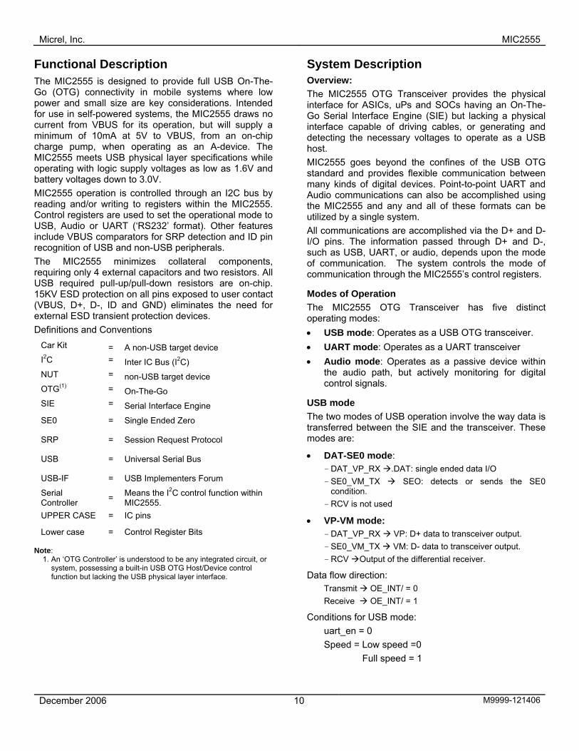
plug can produce multiple rail-to-rail transitions. These will trigger both comparators and produce a conflicting result: ID = GND and ID = Float. The Interrupt source register contains the debounced steady state value of ID. After the nature of the newly connected device has been determined, activating a current source in series with the internal ID pull-up resistor can reduce power consumption caused by ID sensing. This is accomplished by clearing rcs_dis in Control Register 3. When the connected device is removed, and the ID pin is pulled HIGH by the current source (ID=GND is no longer true), MIC2555 automatically resets rcs_dis, disabling the current source.
ID
0.85x
ID Low
100 k
VBAT
Closes to
Open = Reduced 4 µA
0.15x
ID High
1 k
VBAT
VBAT
signalPeripheral
ID sensing current
ID Pin – Operational Diagram
VTRM VBAT powers VTRM, which supplies 3.3V power to the differential USB transmitter and the UART drivers and receivers. As VBAT drops below 3.4V, VTRM is no longer able to regulate and follows VBAT at about 0.1V less than VBAT. When this occurs, output drive levels for USB and UART are reduced accordingly.
Interrupt Detector When in Audio mode, the MIC2555 does not participate in the audio transmissions, but monitors the D+ line for interrupt pulses. If the Serial Controller is configured to flag interrupt pulses, the system controller can exchange both audio signals and digital information with the target device. MIC2555 is designed to detect two different interrupt pulses, those exceeding 3.0V and those crossing the 0.5V level. Under normal circumstances, the audio signal seen on D+ is transposed on a DC level and limited to voltage excursions between the 0.5V and 3.0V levels, so only interrupt pulses should cross these thresholds. Signaling is typically done with only one polarity pulse so MIC2555 is designed to monitor only one threshold at a time. Threshold selection is done with the cr_int_sel bit, and the interrupt (cr_int) can be set to trigger on pulses of either polarity.
UART Mux System controllers with UART communication ability may or may not be able to route their UART signals through the VP, VM or DAT, SE0 pins. For those with independent UART connectivity, MIC2555 provides a secondary UART I/O port. The MUX, under direction of the Serial Controller, selects which UART I/O is used by the OTG controller. Condition: uart_io = 0 SEO_VM_TX = transmit DAT_VP_RX = receive uart_io = 1 GPIO_1_TX = transmit GPIO_0_RX = receive
Differential Driver / Differential Receiver Operation of the Differential Driver and Differential Receiver is described in the tables below and on the following page. The register bits used in the column headings are described in the Serial Controller section of this data sheet.

Micrel, Inc. MIC2555
December 2006 15 M9999-121406
USB mode: uart_en = 0 suspend dat_se0 OE_INT/ RCV DAT_VP SE0_VM D+ D-
0 0 0 DIFF TX data TX data DAT_VP SE0_VM 0 0 1 DIFF SE_DP SE_DM RX data RX data 0 1 0 Z TX data TX data TX_DAT TX_SE0 0 1 1 Z DIFF RX_SE0 RX data RX data 1 0 1 Z SE_DP SE_DM RX data RX data 1 1 1 Z SE_DP RX_SE0 RX data RX data
DIFF = Differential receiver output RX_SE0 = not (SE_DP) and not (SE_DM) TX_DAT = DAT_VP and not (SE0_VM) TX_SE0 = not (DAT_VP) and not (SE0_VM) Z = Tri-State
USB Transmit Operation Inputs Outputs
USB Mode DAT_VP_RX SE0_VM_TX D+ D- RCV
0 0 0 1 unused 1 0 1 0 unused 0 1 0 0 unused
DAT-SE0
1 1 0 0 unused 0 0 0 0 undefined 1 0 1 0 1 0 1 0 1 0
VP-VM
1 1 1 1 undefined The transceiver receives USB data from D+, D- lines when: Conditions: Uart_en = 0 OE_INT/ = 0 Operation of the DAT_VP_RX, SE0_VM_TX and RCV pins during receive is shown on the following page.

Micrel, Inc. MIC2555
December 2006 16 M9999-121406
USB Receive Operation Inputs Outputs
USB Mode Suspend
D+ D- DAT_VP_RX SE0_VM_TX RCV 0 0 0 undefined 1 n/a 0 1 0 1 0 n/a 0 0 1 0 0 n/a 0 1 1 undefined 0 n/a 1 0 0 0 1 n/a 1 1 0 1 0 n/a 1 0 1 0 0 n/a
DAT-SE0
1 1 1 1 0 n/a 0 0 0 0 0 undefined 0 1 0 1 0 1 0 0 1 0 1 0 0 1 1 1 1 undefined 1 0 0 0 0 n/a 1 1 0 1 0 n/a 1 0 1 0 1 n/a
VP-VM
1 1 1 1 1 n/a
If the transceiver is in the DAT-SE0 mode, and the suspend bit has not been set, then the DAT_VP_RX pin always follows the output of the differential receiver during receive operation. The DAT_SE0 pin is not gated by the outputs of the single ended receivers. In the VP-VM mode, the RVC pin always follows the output of the differential receiver. The RVC pin is not gated by the outputs of the singled ended receivers.
UART mode: uart_en = 1 suspend DAT_VP SE0_VM D+ D-
0 SE_DP TX data RX data SE0_VM 1 Z Z Z Z
Z = Tri-State
Single-Ended Receivers The Single Ended Receivers detect the logic levels on the D+ and D- lines, and provide this information to the Single Ended Decoder.
Single-Ended Decoder Behavior of the Single-Ended Decoder is dependent upon the power mode of the transceiver. If transceiver is in the Suspend power mode, and dat_se0 = 1 (DAT-SE0 mode), then the DAT_VP_RX pin will reflect the output of the D+ single ended receiver. This is necessary so that a controller connected to the transceiver can detect data pulsing while the transceiver is in suspended mode.

Micrel, Inc. MIC2555
December 2006 17 M9999-121406
Pin Descriptions VBAT This pin is an input, and supplies power to the transceiver. Transceiver typical operational voltages are between 3.0 V ≤ VBAT ≤ 4.5V and 1.6V < VDD_LGC < VBAT.
VDD_LGC This input is used to set the logic thresholds of the following logic signals: • DAT_VP_RX • SE0_VM_TX • RCV • OE_INT/ • INT/ • ADR0 • RESET/ • GPIO
Important Note: VDD_LGC can be at a voltage less than or equal to VBAT, but never higher than VBAT. Doing so will forward bias internal pad protection diodes and current will flow from VDD_LGC to VBAT. For this reason, systems should not allow VBAT to go to zero while VDD_LGC remains powered. This condition may damage the MIC2555, and could put a severe load on VDD_LGC as it attempts to power the MIC2555 and all other circuits attached to the VBAT line.
VBUS This pin functions as both an input to, and output from, the transceiver. Unlike standard USB transceivers, however, the MIC2555 always derives its operating power from VBAT and never from VBUS. The MIC2555 will supply power to VBUS when acting as a host device and when petitioning another OTG, capable device to become the host. To do so the vbus_chrg bit is asserted. To power VBUS, as a host device, the vbus_drv bit is asserted. The difference between these two controls is vbus_chg applies VTRM (3.3V) to VBUS, where as vbus_driv uses the 5V charge pump output. While VTRM is sufficient for signaling purposes, it does not meet the 4.4V minimum for VBUS.
VTRM VTRM supplies a regulated 3.3V to the D+, D- output drivers, pull-up resistors and other circuitry internal to the MIC2555. A small filter capacitor is required to insure the regulator remains stable under all operating conditions. A good quality 1µF capacitor is sufficient for this purpose.
VTRM can be used to supply small amounts of current to other system functions, typically 3 mA or less. However, trying to source more current can reduce output drive on D+, D- by stealing current from the differential driver.
ID ID detects the arrival or departure of a peripheral device, and differentiates between USB and non-USB devices. To accomplish this, ID is pulled-up by a resistance of approximately 100 kΩ connected to VBAT and the voltage at ID monitored by a set of comparators. When no device is present, ID is pulled high and NO DEVICE condition is reported. When a Mini-A plug is inserted into the system’s Mini-AB receptacle, ID is connected to ground by the Mini-A plug, which triggers the MIC2555 to indicate a USB device is present. Non-USB peripherals use a modified Mini-A plug or non-standard cable assembly with a resistor connected between ID and ground. When connected, this forms a resistor divider such that a voltage of approximately ½ VBAT appears at MIC2555’s ID pin, indicating a non-USB device is present. Additionally, ID can be used to signal non-USB devices. This is accomplished by grounding ID through a low value resistor (~ 1 kΩ), dropping the ID voltage from ½ VBAT to nearly zero, which can be detected by the attached device. This switch is activated by the id_gnd_out bit in Control Register 2.
C-, C+, C++ C-, C+ and C++ are the capacitors required for charge pump operation. C- and C+ are the connections to the ‘flying’ capacitor, which creates the pumping effect. C++ is the reservoir capacitor that stores the 5V supplied to VBUS when vbus_drv is asserted. Because the input source is a low voltage and the charge pump’s regulator is set to limit VOUT to 5V, these capacitors need only be rated at 6 VDC, which helps reduce physical size and cost.
GND_A, GND_D MIC2555 uses separate ground lines within the chip to isolate digital noise from analog signals. Ultimately, these two grounds need to be tied together. This is best done by having both grounds return separately to the power source and join at the bypass capacitor.
RESET/ System reset. Returns all control register bits to their default settings. MIC2555 is not equipped with an internal power-on reset generator, and thus relies upon the system for its reset at power up.

Micrel, Inc. MIC2555
December 2006 18 M9999-121406
DAT_VP_RX, SE0_VM_TX, RCV DAT_VP_RX, SE0_VM_TX and RCV provide the data transfer interface between the system controller and MIC2555. RCV is an output only pin, supplying the output of a differential receiver monitoring the D+, D- pins, while DAT_VP_RX, SE0_VM_TX are bi-directional (I/O) pins and change function in accordance with different USB and UART mode selections. In UART mode, DAT_VP_RX and SE0_VM_TX are the primary data transmit and receive pins. In USB mode, the setting of the dat_se0 determines their action, as described in the tables below.
OE_INT/ The “output enable – interrupt bar” (OE_INT/) pin has three modes of operation, shown in the table below. Suspend modes are controlled by the oe_int_en bit found in Control Register 1.
OE_INT/ Operating Modes suspend oe_int_en I/O Description
0 x Input OE_INT/ acts as output enable, and controls direction of DAT_VP_RX, SE0_VM_TX, D+ and D-
1 0 Input OE_INT/ is an input, but does not control anything 1 1 Output OE_INT/ is asserted low if interrupt condition exists

Micrel, Inc. MIC2555
December 2006 19 M9999-121406
SCL, SDA The serial clock (SCL) and serial data (SDA) signals implement a two-wire I2C serial bus for control of the MIC2555. As with all I2C busses the MIC2555 shares a common external pull-up resistor on each line.
INT/ The interrupt (INT/) pin is asserted while an interrupt condition exists. It is an open drain output so that it can be wire-ORed with other interrupt signals, and requires an external pull-up resistor to provide a logic output. The pull-up voltage must not be greater than VBAT.
ADR0 Because some systems may have more than one transceiver on the I2C bus, OTG Transceivers have been assigned four I2C Address locations by convention. MIC2555 address: 01011xxb (Bit order: A6 A0) The ADR0 pin and MIC2555’s ‘dash number’ control the ‘xx’ of MIC2555’s address, where –0 or –1 specifies the higher order bit’s value:
Part Number Address Range MIC2555BML-0 0x MIC2555BML-1 1x
Where x = the state of ADR0
D+, D- The data plus (D+) and data minus (D-) pins output the USB data signals. When operating as a non-USB transceiver, the role of D+, D- change:
UART mode: D+ = RXD D- = TXD
GPIO_1_TX, GPIO_0_RX, GPIO_2 GPIO_0, GPIO_1, and GPIO_2 are general purpose I/Os that can be used as data ports or interrupt sources for the system controller, display drivers or power switches for actuators or annunciators. These GPIO have open drain outputs capable of sinking at least 10 mA, can be wire ORed together, and may be pulled above the MIC2555’s operating supply voltage, but not beyond the 6V absolute maximum allowed. As logic inputs, the GPIO logic thresholds are standard CMOS thresholds set by VDD_LGC voltage. The GPIO Input Register is a read-only register and shows real time status of the GPIOs, independent of other I/O settings. The GPIO Output Register holds the desired output value for each I/O. Each I/O can act as an independent interrupt source and can be programmed for triggering on T F, F T, or both transitions simultaneously. The GPIO pins serve double duty as active signal pins when called into action by the appropriate control bit:
GPIO_0 = Secondary UART Receive input. GPIO_1 = Secondary UART Transmit output. GPIO_2 = External charge pump oscillator input.
Audio mode: D+ D- Stereo
D+ Mono D- Mic
These are generally agreed upon, but are not mandatory.
Micrel, Inc. MIC2555
December 2006 20 M9999-121406
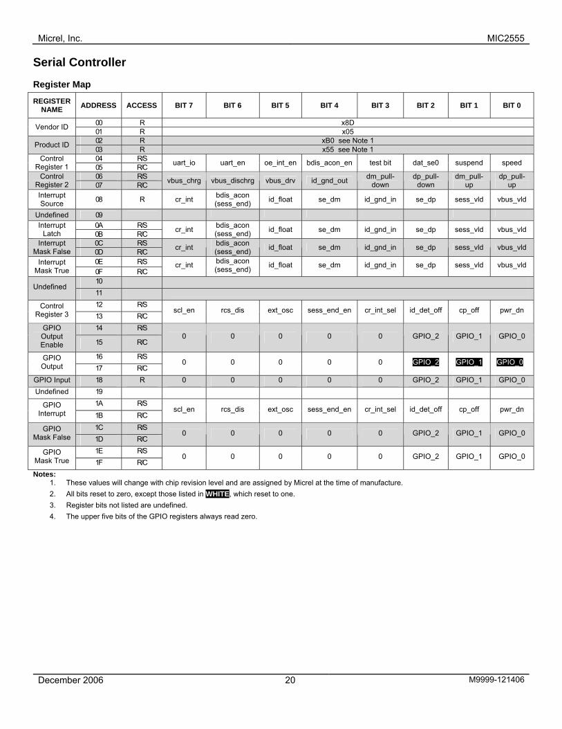
Serial Controller
Register Map
REGISTER NAME ADDRESS ACCESS BIT 7 BIT 6 BIT 5 BIT 4 BIT 3 BIT 2 BIT 1 BIT 0
00 R x8D Vendor ID 01 R x05 02 R xB0 see Note 1 Product ID 03 R x55 see Note 1 04 R/S Control
Register 1 05 R/C uart_io uart_en oe_int_en bdis_acon_en test bit dat_se0 suspend speed
06 R/S Control Register 2 07 R/C vbus_chrg vbus_dischrg vbus_drv id_gnd_out dm_pull-
down dp_pull-
down dm_pull-
up dp_pull-
up Interrupt Source 08 R cr_int bdis_acon
(sess_end) id_float se_dm id_gnd_in se_dp sess_vld vbus_vld
Undefined 09 0A R/S Interrupt
Latch 0B R/C cr_int bdis_acon (sess_end) id_float se_dm id_gnd_in se_dp sess_vld vbus_vld
0C R/S Interrupt Mask False 0D R/C cr_int bdis_acon
(sess_end) id_float se_dm id_gnd_in se_dp sess_vld vbus_vld
0E R/S Interrupt Mask True 0F R/C
cr_int bdis_acon (sess_end) id_float se_dm id_gnd_in se_dp sess_vld vbus_vld
10 Undefined
11 12 R/S Control
Register 3 13 R/C scl_en rcs_dis ext_osc sess_end_en cr_int_sel id_det_off cp_off pwr_dn
14 R/S GPIO Output Enable 15 R/C
0 0 0 0 0 GPIO_2 GPIO_1 GPIO_0
16 R/S GPIO Output 17 R/C
0 0 0 0 0 GPIO_2 GPIO_1 GPIO_00
GPIO Input 18 R 0 0 0 0 0 GPIO_2 GPIO_1 GPIO_0 Undefined 19
1A R/S GPIO Interrupt 1B R/C
scl_en rcs_dis ext_osc sess_end_en cr_int_sel id_det_off cp_off pwr_dn
1C R/S GPIO Mask False 1D R/C
0 0 0 0 0 GPIO_2 GPIO_1 GPIO_0
1E R/S GPIO Mask True 1F R/C
0 0 0 0 0 GPIO_2 GPIO_1 GPIO_0
Notes: 1. These values will change with chip revision level and are assigned by Micrel at the time of manufacture. 2. All bits reset to zero, except those listed in WHITE, which reset to one. 3. Register bits not listed are undefined. 4. The upper five bits of the GPIO registers always read zero.

Micrel, Inc. MIC2555
December 2006 21 M9999-121406
Control Bit Locator Location
Control Bit Control Register 1 Control Register 2 Control Register 3 Interrupt Source GPIO Interrupt
bdis_acon, (sess_end) B6 bdis_acon_en B4 cp_off B1 cr_int B7 cr_int_sel B3 dat_se0 B2 dm_pull-down B3 dm_pull-up B1 dp_pull-down B2 dp_pull-up B0 ext_osc B5 GPIO_0 B0 GPIO_1 B1 GPIO_2 B2 id_det_off B2 id_float B5 id_gnd_in B3 id_gnd_out B4 oe_int_en B5 rcs_dis B6 scl_en B7 se_dm B4 se_dp B2 sess_end_en B4 sess_vld B1 pwr_dn B0 speed B0 suspend B1 test bit B3 uart_en B6 uart_io B7 vbus_chrg B7 vbus_dischrg B6 vbus_drv B5 vbus_vld B0
Serial Controller Register Bits
Example Table Format
Column Titles
Field name Size (bits) Access Register Addresses(1) Description
Note: Access type “rd/s/c” denotes a field that can be read, set to 1 or cleared to 0. The register can be read from either of the Addresses indicated. When writing to the “set” Address, any 1s that are written cause the associated bit to be set. When writing to the “clr” (Clear) Address, any 1s that are written cause the associated bit to be cleared.

Micrel, Inc. MIC2555
December 2006 22 M9999-121406
Device ID Registers
MSB -> Higher byte of two byte wordLSB -> Lower byte of two byte word
vendor_id 16 rd 00h USB-IF Vendor ID number. Address 00h contains lower byte of Vendor ID. Address 01h contains upper byte of Vendor ID.
product_id 16 rd 02h
A number unique to each manufacturer, for each device type produced. The manufacturer assigns this number. Address 02h contains lower byte. Address 03h contains upper byte.
Control Register 1
Set & Clear set – 04h clr – 05h
1 set = 11 clr = 0
speed 1 rd/s/c bit 0 0 = USB Low Speed mode1 = USB Full Speed mode
suspend 1 rd/s/c bit 1 0 = Full power mode 1 = Low power mode
dat_se0 1 rd/s/c bit 2 0 = VP-VM USB mode1 = DAT-SE0 USB mode
test bit 1 rd/s/c bit 3 Not used
bdis_acon_en 1 rd/s/c bit 4 0 = No action. 1 = Attaches pull-up resistor to D+ after detecting SE0 condition and sets interrupt flag.
oe_int_en 1 rd/s/c bit 5
0 = OE_INT/ is an input. 1 = OE_INT/ becomes an output and is asserted LOW when interrupt occurs, if suspend = 1. If suspend = 0, pin remains an input.
uart_en 1 rd/s/c bit 6 0 = USB mode 1 = UART mode
uart_io 1 rd/s/c bit 7
0 = GPIO pins operate as standard GPIO. 1 = GPIO_0 = 2nd UART RX GPIO_1 = 2nd UART TX GPIO_2 = standard GPIO

Micrel, Inc. MIC2555
December 2006 23 M9999-121406
Control Register 2
Set & Clear set – 06h clr – 07h
1 set = 1 1 clr = 0
dp_pull-up 1 rd/s/c bit 0 1 = Connect pull-up to D+
dm_pull-up 1 rd/s/c bit 1 1 = Connect pull-up to D-
dp_pull-down 1 rd/s/c bit 2 1 = Connect pull-down to D+
dm_pull-down 1 rd/s/c bit 3 1 = Connect pull-down to D-
id_gnd_out 1 rd/s/c bit 4 1 = Connect ID pin to ground
vbus_drv 1 rd/s/c bit 5 1 = Power VBUS with charge pump
vbus_dischrg 1 rd/s/c bit 6 1 = Discharge VBUS through a resistor
vbus_chrg 1 rd/s/c bit 7 1 = Charge VBUS through a resistor
Control Register 3
Set & Clear set - 12h clr – 13h
1 set = 1 1 clr = 0
pwr_dn 1 rd/s/c bit 0 1 = Power Down mode.
cp_off 1 rd/s/c bit 1 1 = turns charge pump OFF.(Charge pump generates 5V for powering VBUS)
id_det_off 1 rd/s/c bit 2
0 = ID comparators ON. 1 = Turns ID comparators OFF. Note: Powering down ID comparators does not shut off ID pin pull-up.
cr_int_sel 1 rd/s/c bit 3 Car Kit interrupt select: 0 = Detect < 0.5V level on D+ 1 = Detect > 3.0V level on D+
sess_end_en 1 rd/s/c bit 4
0 = no action. 1 = When bdis_acon_en = 0, switches Bit 6 of the Interrupt Register to indicate Session End comparator status.
ext_osc 1 rd/s/c bit 5 0 = Internal oscillator drives charge pump 1 = External oscillator drives charge pump (Input source = GPIO_2)
rcs_dis 1 rd/s/c bit 6 0 = Activate current source. Weak pull-up on ID pin. 1 = Disable (bypass) current source pull-up on ID pin. Strong pull-up on ID pin.
scl_en 1 rd/s/c bit 7
0 = I2C clock line only transmits. 1 = Bi-directional I2C clock line. Bi-directional clock is required if target device is to be able to control data rate by holding SCL low.

Micrel, Inc. MIC2555
December 2006 24 M9999-121406
Interrupt Source Register
Interrupt Status rd - 08h Indicates the current state of signals that can generate an interrupt.
vbus_vld 1 rd bit 0 1 = VBUS > 4.4V (VBUS valid comparator)
sess_vld 1 rd bit 1 1 = 0.8V< VBUS< 2.0V. (Session valid comparator)
se_dp 1 rd bit 2 1 = D+ pin is HIGH id_gnd_in 1 rd bit 3 1 = ID pin grounded
se_dm 1 rd bit 4 1 = D- pin is HIGH id_float 1 rd bit 5 1 = ID pin floating
bdis_acon (sess_end) 1 rd bit 6
If: bdis_acon_en = 1 1 = SE0 has been detected, transceiver asserted dp_pullup after detecting B-device disconnect. If bdis_acon_en = 0, sess_end_en = 1 1 = VBUS < 0.8V. (Session End comparator output = TRUE)
cr_int 1 rd bit 7 1 = car kit interrupt, D+ pin has seen a pulse above the interrupt level
Interrupt Latch 1
Interrupt Source set –0Ah clr – 0Bh
Indicates which sources have interrupted. 1 = interrupt.
Vbus_vld 1 rd/s/c bit 0 sess_vld 1 rd/s/c bit 1
se_dp 1 rd/s/c bit 2 id_gnd_in 1 rd/s/c bit 3
se_dm 1 rd/s/c bit 4 id_float 1 rd/s/c bit 5
bdis_acon (sess_end) 1 rd/s/c bit 6
cr_int 1 rd/s/c bit 7
Interrupt Mask False
False Interrupt Mask
set – 0Ch clr – 0Dh
Enables interrupts on transition from TRUE to FALSE1 set = 1, Interrupt on T F.1 clr = 0, no interrupt.
Vbus_vld 1 rd/s/c bit 0 sess_vld 1 rd/s/c bit 1
se_dp 1 rd/s/c bit 2 id_gnd_in 1 rd/s/c bit 3
se_dm 1 rd/s/c bit 4 id_float 1 rd/s/c bit 5
bdis_acon (sess_end) 1 rd/s/c bit 6
cr_int 1 rd/s/c bit 7

Micrel, Inc. MIC2555
December 2006 25 M9999-121406
Interrupt Mask True
True Interrupt Mask
set – 0Eh clr – 0Fh
Enables interrupts on transition from FALSE to TRUE. 1 set = 1, Interrupt on F T 1 clr = 0, no interrupt.
vbus_vld 1 rd/s/c bit 0 sess_vld 1 rd/s/c bit 1
se_dp 1 rd/s/c bit 2 id_gnd_in 1 rd/s/c bit 3
se_dm 1 rd/s/c bit 4 id_float 1 rd/s/c bit 5
bdis_acon (sess_end) 1 rd/s/c bit 6
cr_int 1 rd/s/c bit 7

Micrel, Inc. MIC2555
December 2006 26 M9999-121406
GPIO Output Enable
Set & Clear set –14h clr – 15h
1 set = 1, GPIO = OUTPUT. 1 clr = 0, GPIO = INPUT.
GPIO_0 1 rd/s/c bit 0 GPIO_1 1 rd/s/c bit 1 GPIO_2 1 rd/s/c bit 2
1 rd/s/c bit 3 1 rd/s/c bit 4 1 rd/s/c bit 5 1 rd/s/c bit 6 1 rd/s/c bit 7
GPIO Output
Set & Clear set –16h clr – 17h
1 set = 1 at GPIO OUTPUT. 1 clr = 0 at GPIO OUTPUT.
GPIO_0 1 rd/s/c bit 0 GPIO_1 1 rd/s/c bit 1 GPIO_2 1 rd/s/c bit 2
1 rd/s/c bit 3 1 rd/s/c bit 4 1 rd/s/c bit 5 1 rd/s/c bit 6 1 rd/s/c bit 7
GPIO Input Read Status rd – 18h Read current state of GPIO input
GPIO_0 1 rd bit 0 GPIO_1 1 rd bit 1 GPIO_2 1 rd bit 2
1 rd bit 3 1 rd bit 4 1 rd bit 5 1 rd bit 6 1 rd bit 7
GPIO Interrupt Latch
Interrupt Source set –1Ah clr – 1Bh
Indicates which sources have interrupted. 1 = interrupt.
GPIO_0 1 rd/s/c bit 0 GPIO_1 1 rd/s/c bit 1 GPIO_2 1 rd/s/c bit 2 1 rd/s/c bit 3 1 rd/s/c bit 4 1 rd/s/c bit 5 1 rd/s/c bit 6 1 rd/s/c bit 7

Micrel, Inc. MIC2555
December 2006 27 M9999-121406
GPIO Interrupt Mask False
Set & Clear set – 1Ch clr – 1Dh
Enables interrupts on transition from TRUE to FALSE 1 set = 1, Interrupt on T F. 1 clr = 0, no interrupt.
GPIO_0 1 rd/s/c bit 0 GPIO_1 1 rd/s/c bit 1 GPIO_2 1 rd/s/c bit 2
1 rd/s/c bit 3 1 rd/s/c bit 4 1 rd/s/c bit 5 1 rd/s/c bit 6 1 rd/s/c bit 7
GPIO Interrupt Mask True
Set & Clear set – 1Eh clr – 1Fh
Enables interrupts on transition from FALSE to TRUE. 1 set = 1, Interrupt on F T. 1 clr = 0, no interrupt.
GPIO_0 1 rd/s/c bit 0 GPIO_1 1 rd/s/c bit 1 GPIO_2 1 rd/s/c bit 2
1 rd/s/c bit 3 1 rd/s/c bit 4 1 rd/s/c bit 5 1 rd/s/c bit 6 1 rd/s/c bit 7
Note: Access type “rd/s/c” denotes a field that can be read, set to 1 or cleared to 0. The register can be read from either of the Addresses indicated. When writing to the “set” Address, any 1’s that are written cause the associated bit to be set. When writing to the “clr” (Clear) Address, any 1s that are written cause the associated bit to be cleared.
Example Serial Controller Register Settings Example Location Condition BIT 7 BIT 6 BIT 5 BIT 4 BIT 3 BIT 2 BIT 1 BIT 0 Target register Initial state 0 0 1 0 1 0 0 0
‘Set’ register Data loaded into ‘set’ register 1 0 0 0 1 0 0 0
Target register Resulting state 1 0 1 0 1 0 0 0
‘Clear’ register Data loaded into ‘Clear’ register 1 0 0 0 1 0 0 0
Target register Resulting state 0 0 1 0 0 0 0 0

Micrel, Inc. MIC2555
December 2006 28 M9999-121406
PCB Layout Recommendation Although the USB standard and applications are not based in an impedance-controlled environment, a properly designed PCB layout is recommended for optimal transceiver performance. The suggested PCB layout hints are as follows: • Match signal line traces (VP/VM, D+ D–) and try to
keep them as short as possible. • For every signal line trace width (w), separate the
signal lines by 1.5-2 widths. Place all other traces at >2w from all signal line traces.
• Control signal line impedances to ±10%. • Keep Rseries as close to the IC as possible, with
equal distance between Rseries and the IC for both D+ and D–.
Micrel, Inc. MIC2555
December 2006 29 M9999-121406
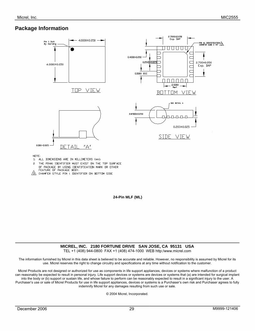
Package Information
24-Pin MLF (ML)
MICREL, INC. 2180 FORTUNE DRIVE SAN JOSE, CA 95131 USA TEL +1 (408) 944-0800 FAX +1 (408) 474-1000 WEB http:/www.micrel.com
The information furnished by Micrel in this data sheet is believed to be accurate and reliable. However, no responsibility is assumed by Micrel for its
use. Micrel reserves the right to change circuitry and specifications at any time without notification to the customer.
Micrel Products are not designed or authorized for use as components in life support appliances, devices or systems where malfunction of a product can reasonably be expected to result in personal injury. Life support devices or systems are devices or systems that (a) are intended for surgical implant
into the body or (b) support or sustain life, and whose failure to perform can be reasonably expected to result in a significant injury to the user. A Purchaser’s use or sale of Micrel Products for use in life support appliances, devices or systems is a Purchaser’s own risk and Purchaser agrees to fully
indemnify Micrel for any damages resulting from such use or sale.
© 2004 Micrel, Incorporated.