Embed Size (px)
Citation preview

Micro to Nano – Scaling Packaging Technologies for Future Microsystems
T. Braun (1), K.-F. Becker (1), J. Bauer (1), F. Hausel (2), B. Pahl (2), O. Wittler (1), R. Mrossko (1), E. Jung (1), A. Ostmann (1), M. Koch (1), V. Bader (1), C. Minge (1), R. Aschenbrenner (1), H. Reichl (2)
(1) Fraunhofer Institute for Reliability and Microintegration
Gustav-Meyer-Allee 25, 13355 Berlin, Germany phone: +49-30/464 03 244 fax: +49-30/464 03 254 e-mail: [email protected]
(2) Technical University Berlin, Microperipheric Center
ABSTRACT As the development of microelectronics is still driving
towards further miniaturization new materials, processes and technologies are crucial for the realization of future cost effective microsystems and components. These future systems will not only consist of SMDs and ICs assembled on a substrate, but will potentially integrate also living cells, organelles, nanocrystals, tubules and other tiny things forming a true Heterogeneous System. Futures ICs and passives will also decrease in size, e.g. for RF-ID applications forecast die sizes are smaller than 250 µm, thicknesses less than 50 µm and pitches way below 100 µm, passives, if not directly integrated into the system carrier, will be even smaller. New placement and joining technologies are demanded for reliable and low cost assembly of such applications, as today’s packaging technologies only allow the assembly of those small dies and components with a very high effort and for this reason with high cost. With ongoing miniaturization also the protection of the microsystems mostly realized by a polymer needs to be decreased in thickness, yet providing maximum protection. Here, besides mechanical stability, humidity barrier functionality is a key factor for system reliability.
Fraunhofer IZMs approaches towards packaging technologies facing the demands of future nano-based Hetero System Integration are described within this paper, comprising material and process development. Material developments focus on nano-particle enhanced polymers. One example are materials with optimized humidity barrier functionality, where various filler particles are integrated into a microelectronic grade epoxy resin and investigated regarding their barrier properties. Furthermore, the processing of nano-particle filled polymers is illustrated.
Process development comprises touchless handling concepts that are promising for handling miniaturized components, not directly fabricated at the very place where they are needed. Different concepts are under evaluation. Magnetic handling can be regarded as one of the most ripened ones, thanks to the rugged approach explored. Another promising concept is the use of microdroplet manipulation by electrowetting. Results from both concepts show potential for future use. Finally advanced interconnect
concepts for low temperature joining by CNT contacts or reactive interconnects are introduced.
In summary an overview on nano-based technologies for heterogeneous system integration is given.
Keywords: nano-particle enhanced materials, touchless handling, electrowetting, heterogeneous integration
1 INTROCUCTION Microelectronics miniaturization has evolved according
to Moore’s law since the mid-sixties and since then it was always possible to succeed in meeting its technological challenges. This might be in question for future applications, as indicated schematically by a red brick wall in the SIA roadmap. Fundamentally new approaches will foster further development in microelectronics. High density integration leads to increased interconnect density and thus to a miniaturization of the individual contacts as well. In parallel to this miniaturization of interconnects, the development of an adapted packaging technology is necessary to provide reliable interconnects from the nano- and micro-scale to the meso-world, where microsystems are used. This paper describes exemplarily research and developments in the area of nano-enhanced packaging materials, touchless positioning of smallest component and new advanced interconnection concepts.
2 NANO-ENHANCED PACKAGING
MATERIALS Filler particles are added to polymers in order to modify
their properties as e.g. thermo-mechanical, electrical, thermal or diffusion behaviour [1]. Therefore, a wide range of different materials are used as fillers. Main class used for microelectronic encapsulants is SiO2 with particle sizes in µm range. These particles allow an adaption of encapsulants, adhesives, coatings or base materials for polymer substrates to microelectronic needs mainly in terms of thermo-mechanical and electrical behaviour. Typical encapsulants as e.g. underfiller, glob tops or epoxy molding compounds have a content of 60 to 80 wt.-% SiO2. Nano-particles may now have the potential to influence the polymer properties significantly only by adding a small amount of fillers.
NSTI-Nanotech 2008, www.nsti.org, ISBN 978-1-4200-8505-1 Vol. 3 161

2.1 Nano-particle enhanced encapsulants with improved moisture resistance
Humidity is always a critical issue in microelectronics where polymers are used as e.g. encapsulants, substrates or adhesives. Water can diffuse into and through the polymer and humidity at bonding interfaces of polymers can lead to a hydrolysis at the interface resulting in delaminations of the polymer. These delaminations can cause two main effects. On the one hand, typically true for encapsulants, mechanical stresses are imposed on interconnects and on the other hand humidity can easily access the interface and can cause corrosion. Both effects have a negative influence on the reliability of the assembly [2, 3]. Water in polymers can also lead to a softening and/or to a swelling of the material resulting in degraded thermo-mechanical properties and higher stresses in a package [4]. Additionally incorporated water can abruptly evaporate during reflow causing a popcorning of the assembly and therewith an irreversible damage. The introduction of high temperature lead-free soldering processes has even increased the importance of this issue. Therefore, polymers with improved moisture resistance and reduced moisture uptake can be one key factor for miniaturization of low cost plastic packaging solutions with constant reliability compared to standard packages.
One possible particle type for humidity resistance enhancement of polymers in microelectronics application could be Bentonite. Bentonite is an aluminium phyllosilicate clay consisting mostly of montmorillonite. The layered structure of the bentonite particles can be dispersed in a polymer. The separated bentonite discs with diameters in the range of 200 – 300 nm and a thickness around 1 nm can act as diffusion path elongation in a polymer [5, 6, 7, 8, 9]. Also water interaction at the particle surface and water uptake of the bentonite itself may influence the diffusion behavior.
Figure 1 shows images from epoxy resins with 2,5 wt.-% content of bentonite I28E from Nanocor (left) and a composition of SiO2 micro particles and I28E bentonite (right). Both images show well exfoliated and dispersed bentonite particles in a microelectronic grade epoxy resin.
Figure 1: TEM image from exfoliated bentonites 2,5 %
(left) and SEM images SiO2 micro-particles with bentonite For direct measuring the diffusion of a nano-particle
modified encapsulant as close as possible to a micro-
electronic application a glob top test vehicle with a bare die humidity sensor SHT 01 from Sensirion was designed. The sensor with a moisture depending capacitor structure on top was glued with a standard die attach adhesive on a substrate. The substrate was fully metallized on the edges and on the bottom to avoid moisture ingress through the substrate. A glob top dam material was used to encapsulate the wire bonds to realize a cavity for the nano-filled polymers. This was needed due to the expected high coefficient of thermal expansion and the high variations of viscosities of the materials applied. For the realization of a homogeneous layer above the sensor area a distance bar was used during epoxy curing. Samples were subjected to 85 °C/85 % r.h. atmosphere and signals of the sensor were collected periodically by a multiplexer.
Figure 2: Moisture concentration (C) at sensor surface
normalized to moisture saturation concentration (Csat), layer thickness are mentioned for different material combinations
Figure 3: Threshold time when moisture concentration
reaches 5 % at sensor surface First results from diffusion measurements with glob top
test vehicle are depicted in Figure 2. The collected moisture concentration data is normalized to the saturation value for all samples. Generally, different behaviour of the material compositions is visible. First the moisture concentration of the unfilled resin increases followed by the bentonite I28E and the combination of I28E with micro-sized SiO2. In Figure 3 the threshold time values where the concentration has reached 5 % are summarized. Here, a significant improvement of the barrier functionality of the bentonite is
1000 10000 100000
0,0
0,2
0,4
0,6
0,8
1,0
unfilled 425 µm 2.5 wt.-% I28E 445 µm 2.5 wt.-% I28E+ 50 wt.-% SiO
2 475 µm
c/c s
at
t [s]
NSTI-Nanotech 2008, www.nsti.org, ISBN 978-1-4200-8505-1 Vol. 3162

visible. The threshold time is around 30 % higher than of the unfilled resin. Due to the high content of micro-sized SiO2 in combination with the bentonite an additional increase occurs. A barrier enhancement could be therewith verified.
3 TOUCHLESS HANDLING
According to ITRS Roadmap for Assembly and Packaging, where experts identify the demands for system packaging for the next 14 years [10], the following specifications will be true for the next generations of System in Package. SiPs will contain both embedded passives & embedded actives; there will be up to 17 dies stacked or otherwise integrated into a package. From year 2010 the I/O count for high performance applications is estimated to be 3506 and will rise up to 5651 in year 2020, for low cost hand held the I/O number will be a stable 800 from year 2008, for RF packages it will be 200 I/Os. Small BGAs / CSPs in their various geometries will be the dominating package type, with Area Array pitches from 200 µm in 2006 down to 150 µm in 2013 and 100 µm in 2020. The components used will be passives of 600x300 µm² in 2008 down to 200x100 µm² in 2020; dies will be thinned down to 50 µm for substrate level assembly and down to 20 µm for wafer level assembly
Touchless and self-assembly based procedures seem to be the only method for handling miniaturized components, not directly fabricated at the very place, where they are needed. In the next section two promising concepts will be presented allowing touchless handlich of smallest components.
3.1 Magnetic handling
To adapt the principles of magnetic handling to processes useful for microelectronics purposes, research projects have been launched at Fraunhofer institutes IZM and IPK. Here focus is put on the examination of basic technological principles of contact-free positioning of small-sized components by use of magnetic fields. The approach is based on well defined interactions of controlled magnetic fields with magnetically addressable components. The situation of movement of such a magnetically interacting component under exposure of a magnetic field is illustrated in Figure 4.
Differing from other contact-free handling principles, magnetic manipulation not necessarily requires the presence of a coupling medium such as water and hence can be performed in dry state.
The crucial point of this approach is to find a suitable configuration of the magnetic field, which exerts such forces on the component needed for a movement in the wanted position. Besides the design of the magnetic field, e.g. in the form of a “magnetic funnel” (see Figure 4), the magnetic properties of the components are essential for the action of the field. Intense study is in progress to calculate the relationships between field strength and characteristics
of the interaction partner such as magnetic permeability and magnetic saturation.
Figure 4: Positioning of a magnetically addressable
component by extern magnetic fields Microelectronic components typically undergo only
inadequate interaction with magnetic fields so that magnetically based positioning procedures fail. To overcome this difficulty, magnetically addressable markers must be designed and attached to the components. An effective technical realization of this principle is the application of thin polymer based layers, filled with magnetically interacting micro- or nano-particles, on top of the components. The layers can be applied cost-effectively on wafer level during fabrication of the components by use of e.g. common stencil printing process; results are shown in Figure 5.
Figure 5: Stencil printed magnetically addressable markers obtained by stencil printing on a 4’’-wafer; left – overview,
right – height profile (maximum 40 µm) The advantage of this approach is the possibility of
generating such patterns of magnetic markers (e.g. lines, curves, dots), that are needed to transform the effect of the magnetic field into the wanted movement of the component. Actual works are focused on the calculation of effective designs of patterns and layer thicknesses of markers and on the development of polymer based magnetically interacting pastes, which can easily be integrated into the process of chip fabrication.
NSTI-Nanotech 2008, www.nsti.org, ISBN 978-1-4200-8505-1 Vol. 3 163

The vision of the complete technological chain of positioning fully disordered components by use of magnetic handling principles could then consist of the sub-processes: separation of the clustered components into single parts, pre-ordering of the components into tracks, rejection of components with wrong z-orientation, precise x-y-positioning by use of magnetic fields.
3.2 Microdroplet manipulation by electro-
wetting
Based on the “electrowetting on dielectric” effect (EWOD) a contactless handling technology well known from lab-on-chip applications for liquid transport, sorting, mixing and splitting will be used as a basis for microelectronics assembly purposes. Handling shall be feasible for miniaturized components as chiplets, smallest SMDs as well as for nano-scaled building blocs, this is currently investigated by Technical University of Berlin in cooperation with TU Freiburg spin-off IMTEK [11]. Physical principle is a change in droplet contact angle when immersed into an electrical field. By applying a moving e-field to the droplet, it can be guided to a defined spot. Using this effect in combination with conventional circuit board technologies might yield a moderate cost approach to exactly place fluid droplets. The use of component laden droplets might be used for contact-less handling of chiplets or all sorts of nano-components (see Figure 6).
Figure 6: Component transport by electrowetting
The process flow under evaluation starts with
positioning of a droplet, containing a component, on a hydrophobic surface of the carrier substrate with rough accuracy takes place (compare Figure 7). Using the mentioned electro wetting effect the droplet will be fast moved until the desired position is reached. The precise placement of the droplet in µm range takes place by means of field gradients and local manipulation of the carrier surface. The assembly is finished with the evaporation of the component containing droplets and the transfer of all components to the final substrate.
Figure 7: Component in microdroplet (left), electrowetting
test vehicle (right)
4 ADVANCED INTERCONNECTS
Interconnection technologies for microelectronics
packaging are currently generated at elevated temperatures, either by soldering, adhesive joining or wire bonding. Typical temperatures for adhesive joining are > 120 °C, for soldering > 250 °C and for Au wire bonding > 120 °C. These temperatures are considered too high for the inter-connection of temperature sensitive components (e.g. bio chips with degradation temperatures ~ 42 °C) or low cost substrates with glass transition temperatures well below 100 °C. There are some potential solutions for this challenge in the market, e.g. Al wire bonding at RT or adhesive joining using low temperature cure isotropic conductive adhesives with cure temperatures down to 80 °C. However, there are limits to the scalability of this processes, so by further re-ducing interconnect dimensions a technological limit will be reached. The use of nanoscale functionalized surfaces for interconnect purposes is seen as a promising means to drive interconnection technology towards smallest geo-metries, in international research a variety of approaches exist (see Figure 8).
100 µm10 nm 100 nm 1 µm 10 µm 1000 µm
NanoVelcro / NanoLawnSolder cap height: 1 µm
Ni-Bump: 3 µm /diam. 12 µmAl-pad opening: 8 µm
Interconnect Pitch
Com
plex
ity
Molecular Modeling
Continuum ApproachFEM Simulation
Low Temperature Interconnect Potential
Surface Activated BondingProf. Suga, Uni Tokyo
Solder Bump / Wire Bond
Cu ColumnsGATech
Nickel Bump / UltraThin Solder Bump
a) Polymer Interconnect – Prior to Bonding C1/C2-mixture
a) Polymer Inte rconnect – After C2 Evaporation / Reaction
Reactive Polymer Interconnect IZM
Bonding at 250-300 °C
Figure 8: Interconnection Technologies development from
micro to nano scale The use of nanoscale modified surfaces for realization
of interconnects in electronics packaging is discussed internationally since several years, but has not yet found their way into industrial applications so far. A mutual approach of Fraunhofer IZM and TU Berlin in Cooperation with the US University of South Florida [UoSF] led to first
NSTI-Nanotech 2008, www.nsti.org, ISBN 978-1-4200-8505-1 Vol. 3164
joining experiments with CNT-covered pads, where weak mechanical and electrical interconnects were created [12].
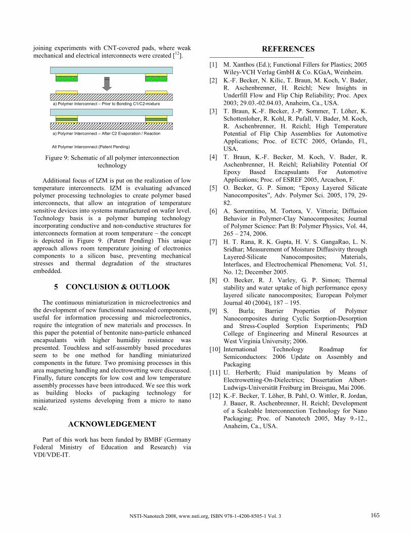
All Polymer Interconnect (Patent Pending)
a) Polymer Interconnect – Prior to Bonding C1/C2-mixture
a) Polymer Interconnect – After C2 Evaporation / Reaction
Figure 9: Schematic of all polymer interconnection
technology
Additional focus of IZM is put on the realization of low temperature interconnects. IZM is evaluating advanced polymer processing technologies to create polymer based interconnects, that allow an integration of temperature sensitive devices into systems manufactured on wafer level. Technology basis is a polymer bumping technology incorporating conductive and non-conductive structures for interconnects formation at room temperature – the concept is depicted in Figure 9. (Patent Pending) This unique approach allows room temperature joining of electronics components to a silicon base, preventing mechanical stresses and thermal degradation of the structures embedded.
5 CONCLUSION & OUTLOOK
The continuous miniaturization in microelectronics and
the development of new functional nanoscaled components, useful for information processing and microelectronics, require the integration of new materials and processes. In this paper the potential of bentonite nano-particle enhanced encapsulants with higher humidity resistance was presented. Touchless and self-assembly based procedures seem to be one method for handling miniaturized components in the future. Two promising processes in this area magneting handling and electrowetting were discussed. Finally, future concepts for low cost and low temperature assembly processes have been introduced. We see this work as building blocks of packaging technology for miniaturized systems developing from a micro to nano scale.
ACKNOWLEDGEMENT
Part of this work has been funded by BMBF (Germany
Federal Ministry of Education and Research) via VDI/VDE-IT.
REFERENCES [1] M. Xanthos (Ed.); Functional Fillers for Plastics; 2005
Wiley-VCH Verlag GmbH & Co. KGaA, Weinheim. [2] K.-F. Becker, N. Kilic, T. Braun, M. Koch, V. Bader,
R. Aschenbrenner, H. Reichl; New Insights in Underfill Flow and Flip Chip Reliability; Proc. Apex 2003; 29.03.-02.04.03, Anaheim, Ca., USA.
[3] T. Braun, K.-F. Becker, J.-P. Sommer, T. Löher, K. Schottenloher, R. Kohl, R. Pufall, V. Bader, M. Koch, R. Aschenbrenner, H. Reichl; High Temperature Potential of Flip Chip Assemblies for Automotive Applications; Proc. of ECTC 2005, Orlando, Fl., USA.
[4] T. Braun, K.-F. Becker, M. Koch, V. Bader, R. Aschenbrenner, H. Reichl; Reliability Potential Of Epoxy Based Encapsulants For Automotive Applications; Proc. of ESREF 2005, Arcachon, F.
[5] O. Becker, G. P. Simon; “Epoxy Layered Silicate Nanocomposites”, Adv. Polymer Sci. 2005, 179, 29-82.
[6] A. Sorrentitino, M. Tortora, V. Vittoria; Diffusion Behavior in Polymer-Clay Nanocomposites; Journal of Polymer Science: Part B: Polymer Physics, Vol. 44, 265 – 274, 2006.
[7] H. T. Rana, R. K. Gupta, H. V. S. GangaRao, L. N. Sridhar; Measurement of Moisture Diffusivity through Layered-Silicate Nanocomposites; Materials, Interfaces, and Electrochemical Phenomena; Vol. 51, No. 12; December 2005.
[8] O. Becker, R. J. Varley, G. P. Simon; Thermal stability and water uptake of high performance epoxy layered silicate nanocomposites; European Polymer Journal 40 (2004), 187 – 195.
[9] S. Burla; Barrier Properties of Polymer Nanocomposites during Cyclic Sorption-Desorption and Stress-Coupled Sorption Experiments; PhD College of Engineering and Mineral Resources at West Virginia University; 2006.
[10] International Technology Roadmap for Semiconductors: 2006 Update on Assembly and Packaging
[11] U. Herberth; Fluid manipulation by Means of Electrowetting-On-Dielectrics; Dissertation Albert-Ludwigs-Universität Freiburg im Breisgau, Mai 2006.
[12] K.-F. Becker, T. Löher, B. Pahl, O. Wittler, R. Jordan, J. Bauer, R. Aschenbrenner, H. Reichl; Development of a Scaleable Interconnection Technology for Nano Packaging; Proc. of Nanotech 2005, May 9.-12., Anaheim, Ca., USA.
NSTI-Nanotech 2008, www.nsti.org, ISBN 978-1-4200-8505-1 Vol. 3 165


![Ebooksclub[1].Org Electronic Device Architectures for the Nano CMOS Era From Ultimate CMOS Scaling to Beyond CMOS Devices](https://img.pdfslide.net/doc/110x75/55720d47497959fc0b8c5b0f/ebooksclub1org-electronic-device-architectures-for-the-nano-cmos-era-from-ultimate-cmos-scaling-to-beyond-cmos-devices.jpg)