Embed Size (px)
Citation preview
Microchip ATMX150RHA Rad-Hard CMOS 150nm cell-based ASIC family
Radiation Characterization Test Report
Total Dose (TID) and Single Event Effects (SEE)
E.Leduca, S.Furica, D.Truyena, D.Danglab
a Microchip Technology Nantes, 44306 Nantes, France
b Centre National d’Etude Spatiale, Toulouse, France
Abstract
Leader of Microcontroller, Mixed-Signal and ASICs solutions
for 30 years, Microchip has developed a large ASICs offer
based on 0.8µm to 150nm technologies.
The ATMX150RHA ASICs offer is based on 150nm SOI
proprietary technology with a Rad-Hard process and standard
cell Library. This technology is powered with a supply
voltage of 1.8V for core and 3.3V for periphery.
The ATMX150RHA will be qualified through ESCC and
DLA standards for ASICs solutions of up to 22 million
routable gates.
Mixed-signal challenge has been addressed through a fully
electrical and radiation characterization of elementary
devices, using different test chips: Standard Evaluation
Circuit (SEC) & Analog Test Vehicle dedicated to:
• Digital blocks: hardened standard-cells, hardened Flip-
Flops & compiled memories
• Analog IPs: Voltage regulator & reference, clock
synthesizer & signal conditioning
A large choice of devices is available as MOS 1.8V, 3.3V,
5V, 15V and LDMOS 25V&45V, developed and simulated in
the range of -55°C to 145°C junction temperature.
This paper presents the current radiation overview of the
ATMX150RHA devices contained in the PDK. The following
items are covered: Single Event Latch-up (SEL), Single Event
Transient (SET) & Single Event Upset (SEU), Single Event
Gate Rupture (SEGR) & Single Event Burn-out (SEB) for HV
devices and finally Total Ionizing Dose (TID).
I. INTRODUCTION
This report is devoted to the radiation characterization of
ATMX150RHA, and gives a summary of the main radiation
results obtained on elementary devices. The quality assurance
grade is given for each device, and the associated electrical
rules and recommendations are given for space applications.
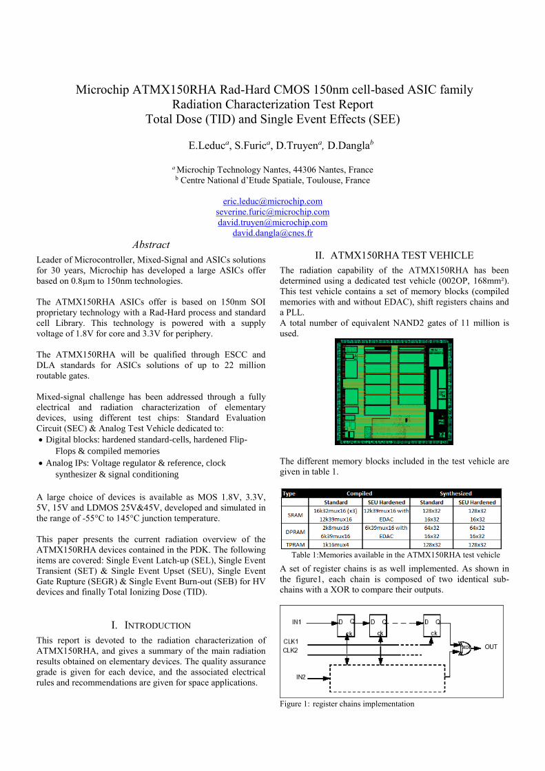
II. ATMX150RHA TEST VEHICLE
The radiation capability of the ATMX150RHA has been
determined using a dedicated test vehicle (002OP, 168mm²).
This test vehicle contains a set of memory blocks (compiled
memories with and without EDAC), shift registers chains and
a PLL.
A total number of equivalent NAND2 gates of 11 million is
used.
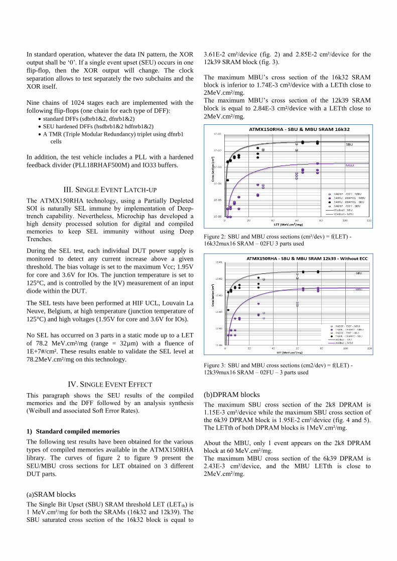
The different memory blocks included in the test vehicle are
given in table 1.
Table 1:Memories available in the ATMX150RHA test vehicle
A set of register chains is as well implemented. As shown in
the figure1, each chain is composed of two identical sub-
chains with a XOR to compare their outputs.
Figure 1: register chains implementation
In standard operation, whatever the data IN pattern, the XOR
output shall be ‘0’. If a single event upset (SEU) occurs in one
flip-flop, then the XOR output will change. The clock
separation allows to test separately the two subchains and the
XOR itself.
Nine chains of 1024 stages each are implemented with the
following flip-flops (one chain for each type of DFF):
• standard DFFs (sdbrb1&2, dfnrb1&2)
• SEU hardened DFFs (hsdbrb1&2 hdfnrb1&2)
• A TMR (Triple Modular Redundancy) triplet using dfnrb1
cells
In addition, the test vehicle includes a PLL with a hardened
feedback divider (PLL18RHAF500M) and IO33 buffers.
III. SINGLE EVENT LATCH-UP
The ATMX150RHA technology, using a Partially Depleted
SOI is naturally SEL immune by implementation of Deep-
trench capability. Nevertheless, Microchip has developed a
high density processed solution for digital and compiled
memories to keep SEL immunity without using Deep
Trenches.
During the SEL test, each individual DUT power supply is
monitored to detect any current increase above a given
threshold. The bias voltage is set to the maximum Vcc; 1.95V
for core and 3.6V for IOs. The junction temperature is set to
125°C, and is controlled by the I(V) measurement of an input
diode within the DUT.
The SEL tests have been performed at HIF UCL, Louvain La
Neuve, Belgium, at high temperature (junction temperature of
125°C) and high voltages (1.95V for core and 3.6V for IOs).
No SEL has occurred on 3 parts in a static mode up to a LET
of 78.2 MeV.cm²/mg (range = 32µm) with a fluence of
1E+7#/cm². These results enable to validate the SEL level at
78.2MeV.cm²/mg on this technology.
IV. SINGLE EVENT EFFECT
This paragraph shows the SEU results of the compiled
memories and the DFF followed by an analysis synthesis
(Weibull and associated Soft Error Rates).
1) Standard compiled memories
The following test results have been obtained for the various
types of compiled memories available in the ATMX150RHA
library. The curves of figure 2 to figure 9 present the
SEU/MBU cross sections for LET obtained on 3 different
DUT parts.
(a) SRAM blocks
The Single Bit Upset (SBU) SRAM threshold LET (LETth) is
1 MeV.cm²/mg for both the SRAMs (16k32 and 12k39). The
SBU saturated cross section of the 16k32 block is equal to
3.61E-2 cm²/device (fig. 2) and 2.85E-2 cm²/device for the
12k39 SRAM block (fig. 3).
The maximum MBU’s cross section of the 16k32 SRAM
block is inferior to 1.74E-3 cm²/device with a LETth close to
2MeV.cm²/mg.
The maximum MBU’s cross section of the 12k39 SRAM
block is equal to 2.84E-3 cm²/device with a LETth close to
2MeV.cm²/mg.
Figure 2: SBU and MBU cross sections (cm²/dev) = f(LET) -
16k32mux16 SRAM – 02FU 3 parts used
Figure 3: SBU and MBU cross sections (cm2/dev) = f(LET) -
12k39mux16 SRAM – 02FU – 3 parts used
(b) DPRAM blocks
The maximum SBU cross section of the 2k8 DPRAM is
1.15E-3 cm²/device while the maximum SBU cross section of
the 6k39 DPRAM block is 1.95E-2 cm²/device (fig. 4 and 5).
The LETth of both DPRAM blocks is 1MeV.cm²/mg.
About the MBU, only 1 event appears on the 2k8 DPRAM
block at 60 MeV.cm²/mg.
The maximum MBU cross section of the 6k39 DPRAM is
2.43E-3 cm²/device, and the MBU LETth is close to
2MeV.cm²/mg.
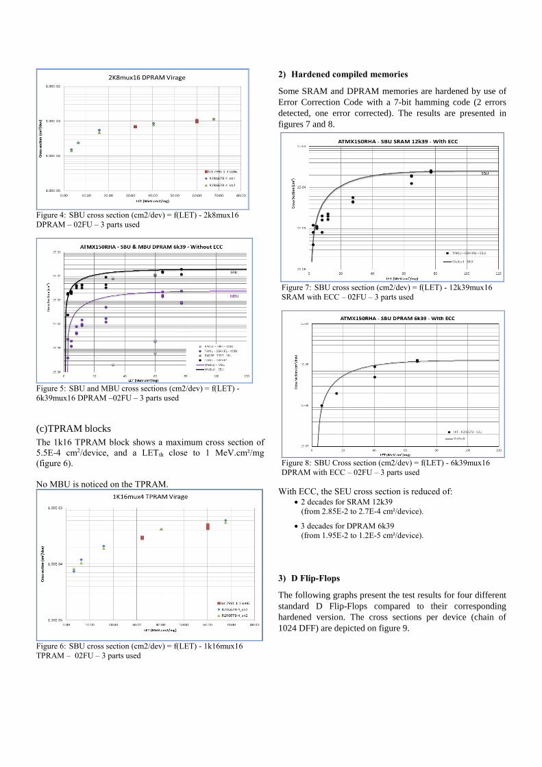
Figure 4: SBU cross section (cm2/dev) = f(LET) - 2k8mux16
DPRAM – 02FU – 3 parts used
Figure 5: SBU and MBU cross sections (cm2/dev) = f(LET) -
6k39mux16 DPRAM –02FU – 3 parts used
(c) TPRAM blocks
The 1k16 TPRAM block shows a maximum cross section of
5.5E-4 cm2/device, and a LETth close to 1 MeV.cm²/mg
(figure 6).
No MBU is noticed on the TPRAM.
Figure 6: SBU cross section (cm2/dev) = f(LET) - 1k16mux16
TPRAM – 02FU – 3 parts used
2) Hardened compiled memories
Some SRAM and DPRAM memories are hardened by use of
Error Correction Code with a 7-bit hamming code (2 errors
detected, one error corrected). The results are presented in
figures 7 and 8.
Figure 7: SBU cross section (cm2/dev) = f(LET) - 12k39mux16
SRAM with ECC – 02FU – 3 parts used
Figure 8: SBU Cross section (cm2/dev) = f(LET) - 6k39mux16
DPRAM with ECC – 02FU – 3 parts used
With ECC, the SEU cross section is reduced of: • 2 decades for SRAM 12k39
(from 2.85E-2 to 2.7E-4 cm²/device).
• 3 decades for DPRAM 6k39
(from 1.95E-2 to 1.2E-5 cm²/device).
3) D Flip-Flops
The following graphs present the test results for four different
standard D Flip-Flops compared to their corresponding
hardened version. The cross sections per device (chain of
1024 DFF) are depicted on figure 9.
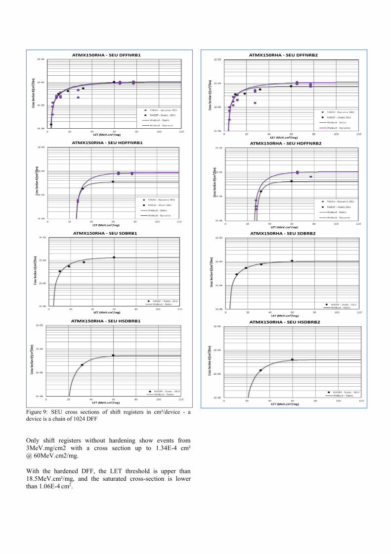
Figure 9: SEU cross sections of shift registers in cm²/device - a
device is a chain of 1024 DFF
Only shift registers without hardening show events from
3MeV.mg/cm2 with a cross section up to 1.34E-4 cm²
@ 60MeV.cm2/mg.
With the hardened DFF, the LET threshold is upper than
18.5MeV.cm²/mg, and the saturated cross-section is lower
than 1.06E-4 cm2.
4) SEU analysis for Memories and DFF
(a) LET threshold and cross section
The tables 2 & 3 summarize the LET threshold, cross section
and W and S Weibull parameters derived from the SEE test
results obtained for the various tested elements.
Table 3:Summary of the LET threshold and cross section for the
DFF – a device is a chain of 1024
(b) Soft Error Rate estimation
SEU error rate calculation has been made using OMERE 4.2
for some examples of orbits and conditions. The calculated
error rates are presented in tables 4 to 13.
Environment conditions:
Estimation of error rate in space (SER protons estimated by
PROFIT) using OMERE.
Solar Min, Z=1 to 92, Aluminium shielding of 1g/cm2.
The Weibull parameters (table 2 & 3) allow to simulate other
space conditions and evaluate the probability of errors for a
dedicated space mission.
Table 4:Estimation of SBU error rate for SRAM.
Table 5:Estimation of SBU error for DPRAM.
Table 6:Estimation of SBU error rate for TPRAM.
Table 7:Estimation of SBU error rate for DPRAM/SRAM with
ECC.
Table 8:Estimation of MBU error rate per device for SRAM.
Table 9:Estimation of MBU error rate per device for DPRAM.
Memory
type
LET threshold
(MeV.cm²/mg)
SEU Xs
(cm2/dev)
Weibull param.
W S
SRAM16k32 1 3.61E-2 24 1.2
SRAM12k39 1 2.85E-2 24 1.2
DPRAM6k39
DPRAM2k8
1
1
1.95E-2
1.15E-3
22
25
1.0
0.9
TPRAM 1k16 1 5.55E-4 30 0.8
SRAM12k39
with ECC 1 2.56E-4 30 1.3
DPRAM6k39
with ECC 3.3 1.30E-5 28 1.2
Memory
type
LET threshold
(MeV.cm²/mg)
MBU Xs
(cm2/dev)
Weibull param.
W S
SRAM16k32 2 1.74E-3 40 1.8
SRAM12k39 2 2.84E-3 40 1.8
DPRAM6k39 2 2.43E-3 34 1.4
Table 2:Summary of the SBU/MBU LET threshold and cross
section for the memories
DFF
type
LET threshold
(MeV.cm²/mg)
SEU Xs
(cm2/dev)
Weibull param.
W S
DFFNRB1 3.0 1.08E-4 22 1.0
DFFNRB2 3.6 1.14E-4 22 1.0
SEU hard.
DFFNRB1 26 8.70E-5 16 1.2
SEU hard.
DFFNRB2 26 1.06E-4 16 1.2
Scan Std DFF
SDBRB1 3.6 1.34E-4 20 1.3
Scan Std DFF
SDBRB2 3.6 1.06E-4 20 1.1
Scan SEU hard.
DFF SDBRB1 18.5 5.25E-5 20 1.7
Scan SEU hard.
DFF SDBRB2 18.5 4.00E-5 22 1.7
TMR - std
DFFs NA 0 NA NA
PLL(*) 1 NA NA NA
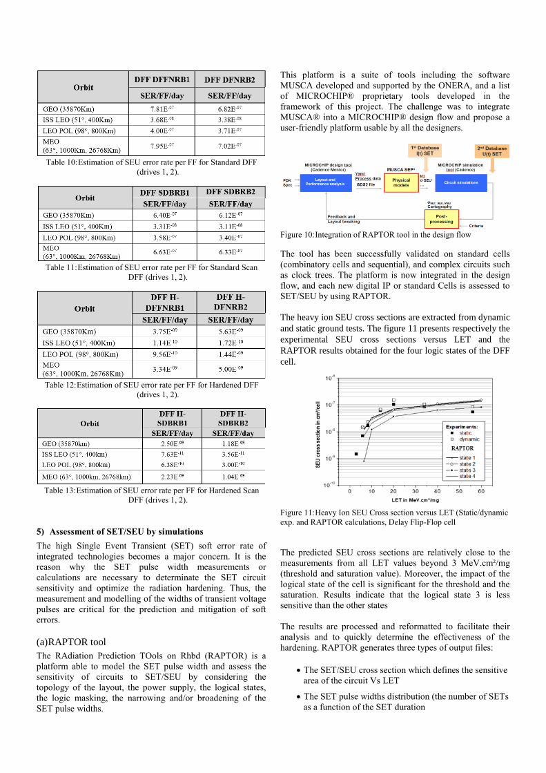
Table 10: Estimation of SEU error rate per FF for Standard DFF
(drives 1, 2).
Table 11: Estimation of SEU error rate per FF for Standard Scan
DFF (drives 1, 2).
Table 12: Estimation of SEU error rate per FF for Hardened DFF
(drives 1, 2).
Table 13: Estimation of SEU error rate per FF for Hardened Scan
DFF (drives 1, 2).
5) Assessment of SET/SEU by simulations
The high Single Event Transient (SET) soft error rate of
integrated technologies becomes a major concern. It is the
reason why the SET pulse width measurements or
calculations are necessary to determinate the SET circuit
sensitivity and optimize the radiation hardening. Thus, the
measurement and modelling of the widths of transient voltage
pulses are critical for the prediction and mitigation of soft
errors.
(a) RAPTOR tool
The RAdiation Prediction TOols on Rhbd (RAPTOR) is a
platform able to model the SET pulse width and assess the
sensitivity of circuits to SET/SEU by considering the
topology of the layout, the power supply, the logical states,
the logic masking, the narrowing and/or broadening of the
SET pulse widths.
This platform is a suite of tools including the software
MUSCA developed and supported by the ONERA, and a list
of MICROCHIP® proprietary tools developed in the
framework of this project. The challenge was to integrate
MUSCA® into a MICROCHIP® design flow and propose a
user-friendly platform usable by all the designers.
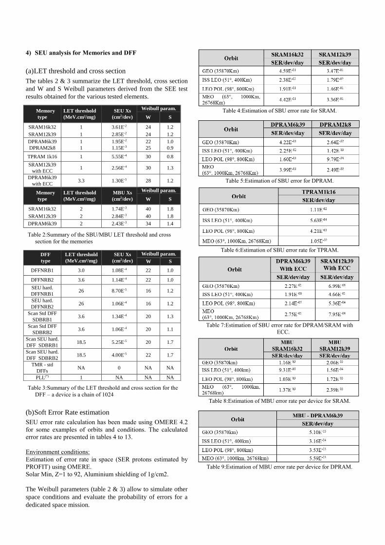
Figure 10: Integration of RAPTOR tool in the design flow
The tool has been successfully validated on standard cells
(combinatory cells and sequential), and complex circuits such
as clock trees. The platform is now integrated in the design
flow, and each new digital IP or standard Cells is assessed to
SET/SEU by using RAPTOR.
The heavy ion SEU cross sections are extracted from dynamic
and static ground tests. The figure 11 presents respectively the
experimental SEU cross sections versus LET and the
RAPTOR results obtained for the four logic states of the DFF
cell.
Figure 11: Heavy Ion SEU Cross section versus LET (Static/dynamic
exp. and RAPTOR calculations, Delay Flip-Flop cell
The predicted SEU cross sections are relatively close to the
measurements from all LET values beyond 3 MeV.cm²/mg
(threshold and saturation value). Moreover, the impact of the
logical state of the cell is significant for the threshold and the
saturation. Results indicate that the logical state 3 is less
sensitive than the other states
The results are processed and reformatted to facilitate their
analysis and to quickly determine the effectiveness of the
hardening. RAPTOR generates three types of output files:
• The SET/SEU cross section which defines the sensitive
area of the circuit Vs LET
• The SET pulse widths distribution (the number of SETs
as a function of the SET duration
• The mapping of the SET/SEU sensitivity on the layout
of the circuit
The adding value of RAPTOR is its ability to assess easily,
and in a short time the radiation sensitivity of a circuit, IP or
standard cell. The effort deployed on the user-friendly
interface is a plus for the analysis. Thus, RAPTOR is a key
tool to improve the customer support on the radiation
hardening.
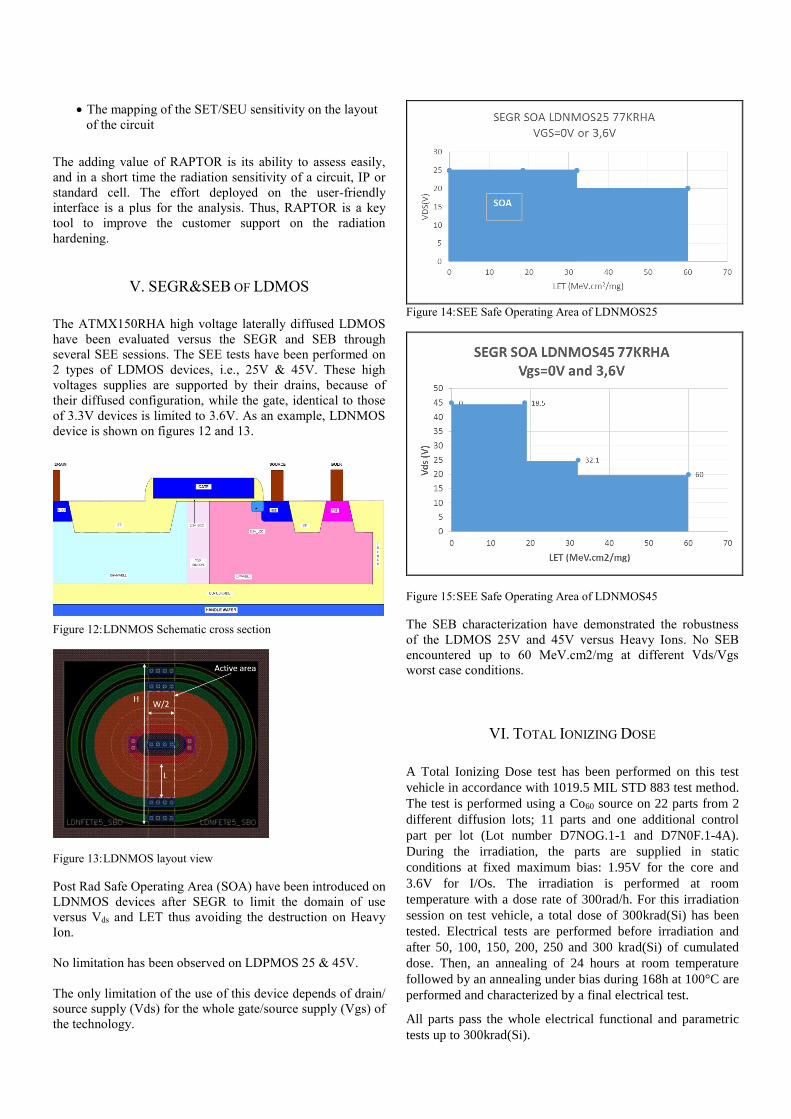
V. SEGR&SEB OF LDMOS
The ATMX150RHA high voltage laterally diffused LDMOS
have been evaluated versus the SEGR and SEB through
several SEE sessions. The SEE tests have been performed on
2 types of LDMOS devices, i.e., 25V & 45V. These high
voltages supplies are supported by their drains, because of
their diffused configuration, while the gate, identical to those
of 3.3V devices is limited to 3.6V. As an example, LDNMOS
device is shown on figures 12 and 13.
Figure 12: LDNMOS Schematic cross section
Figure 13: LDNMOS layout view
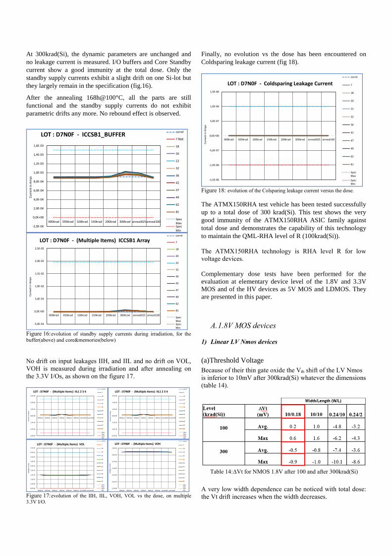
Post Rad Safe Operating Area (SOA) have been introduced on
LDNMOS devices after SEGR to limit the domain of use
versus Vds and LET thus avoiding the destruction on Heavy
Ion.
No limitation has been observed on LDPMOS 25 & 45V.
The only limitation of the use of this device depends of drain/
source supply (Vds) for the whole gate/source supply (Vgs) of
the technology.
Figure 14: SEE Safe Operating Area of LDNMOS25
Figure 15: SEE Safe Operating Area of LDNMOS45
The SEB characterization have demonstrated the robustness
of the LDMOS 25V and 45V versus Heavy Ions. No SEB
encountered up to 60 MeV.cm2/mg at different Vds/Vgs
worst case conditions.
VI. TOTAL IONIZING DOSE
A Total Ionizing Dose test has been performed on this test
vehicle in accordance with 1019.5 MIL STD 883 test method.
The test is performed using a Co60 source on 22 parts from 2
different diffusion lots; 11 parts and one additional control
part per lot (Lot number D7NOG.1-1 and D7N0F.1-4A).
During the irradiation, the parts are supplied in static
conditions at fixed maximum bias: 1.95V for the core and
3.6V for I/Os. The irradiation is performed at room
temperature with a dose rate of 300rad/h. For this irradiation
session on test vehicle, a total dose of 300krad(Si) has been
tested. Electrical tests are performed before irradiation and
after 50, 100, 150, 200, 250 and 300 krad(Si) of cumulated
dose. Then, an annealing of 24 hours at room temperature
followed by an annealing under bias during 168h at 100°C are
performed and characterized by a final electrical test.
All parts pass the whole electrical functional and parametric
tests up to 300krad(Si).
At 300krad(Si), the dynamic parameters are unchanged and
no leakage current is measured. I/O buffers and Core Standby
current show a good immunity at the total dose. Only the
standby supply currents exhibit a slight drift on one Si-lot but
they largely remain in the specification (fig.16).
After the annealing 168h@100°C, all the parts are still
functional and the standby supply currents do not exhibit
parametric drifts any more. No rebound effect is observed.
-2,0E-04
0,0E+00
2,0E-04
4,0E-04
6,0E-04
8,0E-04
1,0E-03
1,2E-03
1,4E-03
1,6E-03
000krad 050krad 100krad 150krad 200krad 300krad anneal025anneal100
Cu
rren
t in
Am
ps
LOT : D7N0F - ICCSB1_BUFFER correl
7
18
20
22
32
36
42
47
49
62
81
SpecMaxSpecMin
-5,0E-03
0,0E+00
5,0E-03
1,0E-02
1,5E-02
2,0E-02
2,5E-02
000krad 050krad 100krad 150krad 200krad 300krad anneal025 anneal100
Cu
rren
t in
Am
ps
LOT : D7N0F - (Multiple Items) ICCSB1 Arraycorrel
7
18
20
22
32
36
42
47
49
62
81
SpecMaxSpecMin
Figure 16: evolution of standby supply currents during irradiation, for the
buffer(above) and core&memories(below)
No drift on input leakages IIH, and IIL and no drift on VOL,
VOH is measured during irradiation and after annealing on
the 3.3V I/Os, as shown on the figure 17.
-6,0E-06
-4,0E-06
-2,0E-06
0,0E+00
2,0E-06
4,0E-06
6,0E-06
000krad 050krad 100krad 150krad 200krad 300krad anneal025 anneal100
Cu
rren
t in
Am
ps
LOT : D7N0F - (Multiple Items) IIL1 2 3 4correl
7
18
20
22
32
36
42
47
49
62
81
SpecMaxSpecMin
-6,0E-06
-4,0E-06
-2,0E-06
0,0E+00
2,0E-06
4,0E-06
6,0E-06
000krad 050krad 100krad 150krad 200krad 300krad anneal025 anneal100
Cu
rren
t in
Am
ps
LOT : D7N0F - (Multiple Items) IIL1 2 3 4correl
7
18
20
22
32
36
42
47
49
62
81
SpecMaxSpecMin
0.0E+00
5.0E-02
1.0E-01
1.5E-01
2.0E-01
2.5E-01
3.0E-01
3.5E-01
4.0E-01
4.5E-01
000krad 050krad 100krad 150krad 200krad 300krad anneal025 anneal100
Vo
ltag
e in
Vo
lts
LOT : D7N0F - (Multiple Items) VOLcorrel
7
18
20
22
32
36
42
47
49
62
81
SpecMaxSpecMin
2,5E+00
2,6E+00
2,6E+00
2,7E+00
2,7E+00
2,8E+00
2,8E+00
000krad 050krad 100krad 150krad 200krad 300krad anneal025 anneal100
Vo
lta
ge in
Vo
lts
LOT : D7N0F - (Multiple Items) VOHcorrel
7
18
20
22
32
36
42
47
49
62
81
SpecMaxSpecMin
Figure 17: evolution of the IIH, IIL, VOH, VOL vs the dose, on multiple
3.3V I/O.
Finally, no evolution vs the dose has been encountered on
Coldsparing leakage current (fig 18).
-1,5E-06
-1,0E-06
-5,0E-07
0,0E+00
5,0E-07
1,0E-06
1,5E-06
000krad 050krad 100krad 150krad 200krad 300krad anneal025 anneal100
Cu
rren
t in
Am
ps
LOT : D7N0F - Coldsparing Leakage Current
correl
7
18
20
22
32
36
42
47
49
62
81
SpecMax
SpecMin
Figure 18: evolution of the Colsparing leakage current versus the dose.
The ATMX150RHA test vehicle has been tested successfully
up to a total dose of 300 krad(Si). This test shows the very
good immunity of the ATMX150RHA ASIC family against
total dose and demonstrates the capability of this technology
to maintain the QML-RHA level of R (100krad(Si)).
The ATMX150RHA technology is RHA level R for low
voltage devices.
Complementary dose tests have been performed for the
evaluation at elementary device level of the 1.8V and 3.3V
MOS and of the HV devices as 5V MOS and LDMOS. They
are presented in this paper.
A. 1.8V MOS devices
1) Linear LV Nmos devices
(a) Threshold Voltage
Because of their thin gate oxide the Vth shift of the LV Nmos
is inferior to 10mV after 300krad(Si) whatever the dimensions
(table 14).
Table 14: Vt for NMOS 1.8V after 100 and after 300krad(Si)
A very low width dependence can be noticed with total dose:
the Vt drift increases when the width decreases.
Ref.
-1.2E-02
-1.0E-02
-8.0E-03
-6.0E-03
-4.0E-03
-2.0E-03
0.0E+00
2.0E-03
4.0E-03
0 2 4 6 8 10 12
V
t e
n V
olt
s
Width (µm)
Max Vt versus W NMOS
100Krad
300Krad
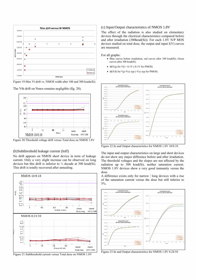
Figure 19: Max Vt drift vs. NMOS width after 100 and 300 krads(Si).
The Vth drift on Nmos remains negligible (fig. 20).
Figure 20: Threshold voltage drift versus Total dose on NMOS 1.8V
(b) Subthreshold leakage current (Ioff)
No drift appears on NMOS short device in term of leakage
current. Only a very slight increase can be observed on long
devices but this drift is inferior to ½ decade at 300 krad(Si).
This drift is totally recovered after annealing.
Figure 21: Subthreshold current versus Total dose on NMOS 1.8V
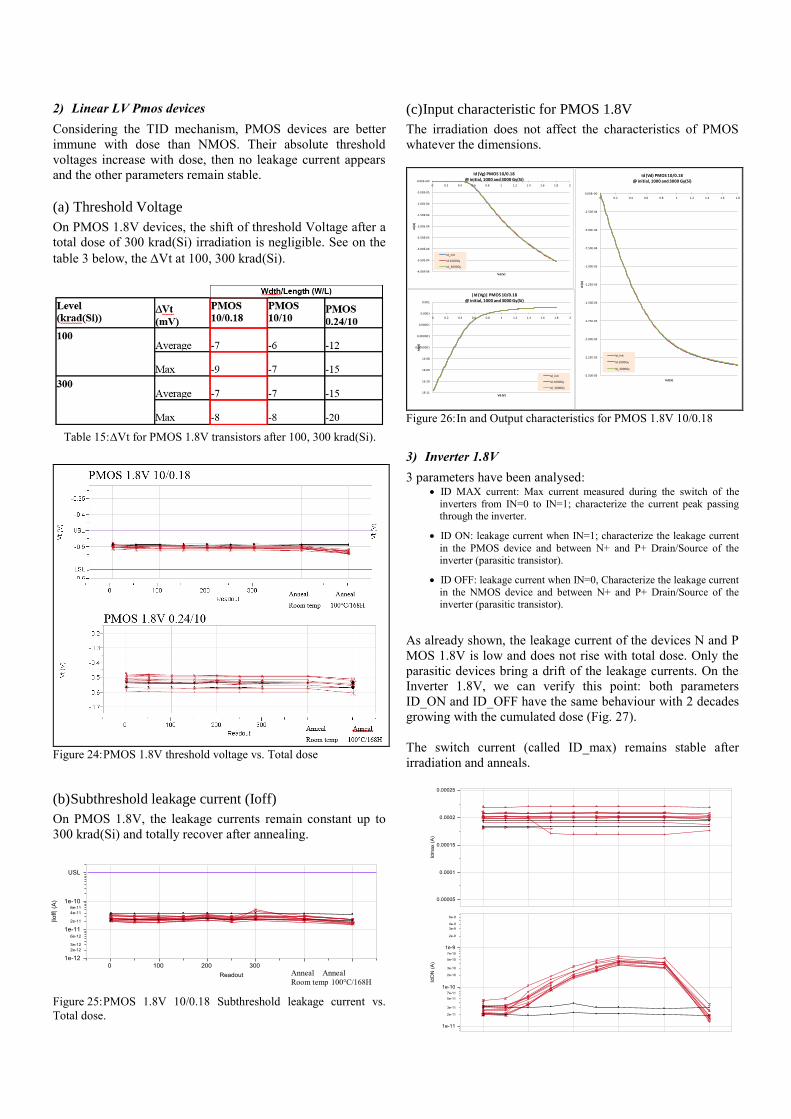
(c) Input/Output characteristics of NMOS 1.8V
The effect of the radiation is also studied on elementary
devices through the electrical characteristics compared before
and after irradiation (300krad(Si)). For each 1.8V N/P MOS
devices studied on total dose, the output and input I(V) curves
are measured.
For all graphs: • Blue curves before irradiation, red curves after 100 krad(Si), Green
curves after 300 krad(Si)
• Id(Vg) for Vd = 0.1V (-0.1V for PMOS)
• Id(Vd) for Vg=Vcc typ (-Vcc typ for PMOS)
0.00E+00
1.00E-04
2.00E-04
3.00E-04
4.00E-04
5.00E-04
6.00E-04
7.00E-04
8.00E-04
9.00E-04
1.00E-03
0 0.2 0.4 0.6 0.8 1 1.2 1.4 1.6 1.8 2
Id (A
)
Vd (V)
Id (Vg) NMOS 10/0.18@ initial, 1000 and 3000 Gy(Si)
Id_init
Id-1000Gy
Id_3000Gy
1.00E-11
1.00E-10
1.00E-09
1.00E-08
1.00E-07
1.00E-06
1.00E-05
1.00E-04
1.00E-03
1.00E-02
1.00E-01
0 0.2 0.4 0.6 0.8 1 1.2 1.4 1.6 1.8 2
Id (A
)
Vd (V)
Id (Vg) NMOS 10/0.18@ initial, 1000 and 3000 Gy(Si)
Id_init
Id-1000Gy
Id_3000Gy
0.00E+00
5.00E-04
1.00E-03
1.50E-03
2.00E-03
2.50E-03
3.00E-03
3.50E-03
4.00E-03
4.50E-03
5.00E-03
0 0.2 0.4 0.6 0.8 1 1.2 1.4 1.6 1.8
Id (A
)
Vd (V)
Id (Vd) NMOS 10/0.18@ initial, 1000 and 3000 Gy(Si)
Id_init
Id-1000Gy
Id_3000Gy
Figure 22: In and Output characteristics for NMOS 1.8V 10/0.18.
The input and output characteristics on large and short devices
do not show any major difference before and after irradiation.
The threshold voltages and the slopes are not affected by the
radiation up to 300 krad(Si), neither saturation current.
NMOS 1.8V devices show a very good immunity versus the
dose.
A difference exists only for narrow / long devices with a rise
of the saturation current versus the dose but still inferior to
5%.
0.00E+00
1.00E-07
2.00E-07
3.00E-07
4.00E-07
5.00E-07
6.00E-07
7.00E-07
0 0.2 0.4 0.6 0.8 1 1.2 1.4 1.6 1.8 2
Id (A
)
Vd (V)
Id (Vg) NMOS 0.24/10@ initial, 1000 and 3000 Gy(Si)
Id_init
Id-1000Gy
Id_3000Gy
1.00E-12
1.00E-11
1.00E-10
1.00E-09
1.00E-08
1.00E-07
1.00E-06
1.00E-05
0 0.2 0.4 0.6 0.8 1 1.2 1.4 1.6 1.8 2
Id (A
)
Vd (V)
Id (Vg) NMOS 0.24/10@ initial, 1000 and 3000 Gy(Si)
Id_init
Id-1000Gy
Id_3000Gy
0.00E+00
1.00E-06
2.00E-06
3.00E-06
4.00E-06
5.00E-06
6.00E-06
0 0.2 0.4 0.6 0.8 1 1.2 1.4 1.6 1.8
Id (A
)
Vd (V)
Id (Vd) NMOS 0.24/10@ initial, 1000 and 3000 Gy(Si)
Id_init
Id-1000Gy
Id_3000Gy
Figure 23: In and Output characteristics for NMOS 1.8V 0.24/10
2) Linear LV Pmos devices
Considering the TID mechanism, PMOS devices are better
immune with dose than NMOS. Their absolute threshold
voltages increase with dose, then no leakage current appears
and the other parameters remain stable.
(a) Threshold Voltage
On PMOS 1.8V devices, the shift of threshold Voltage after a
total dose of 300 krad(Si) irradiation is negligible. See on the
table 3 below, the Vt at 100, 300 krad(Si).
Table 15: Vt for PMOS 1.8V transistors after 100, 300 krad(Si).
Figure 24: PMOS 1.8V threshold voltage vs. Total dose
(b) Subthreshold leakage current (Ioff)
On PMOS 1.8V, the leakage currents remain constant up to
300 krad(Si) and totally recover after annealing.
Figure 25: PMOS 1.8V 10/0.18 Subthreshold leakage current vs.
Total dose.
(c) Input characteristic for PMOS 1.8V
The irradiation does not affect the characteristics of PMOS
whatever the dimensions.
-4.00E-04
-3.50E-04
-3.00E-04
-2.50E-04
-2.00E-04
-1.50E-04
-1.00E-04
-5.00E-05
0.00E+00
0 0.2 0.4 0.6 0.8 1 1.2 1.4 1.6 1.8 2
Id (A
)
Vd (V)
Id (Vg) PMOS 10/0.18@ initial, 1000 and 3000 Gy(Si)
Id_init
Id-1000Gy
Id_3000Gy
1E-11
1E-10
1E-09
1E-08
0.0000001
0.000001
0.00001
0.0001
0.001
0 0.2 0.4 0.6 0.8 1 1.2 1.4 1.6 1.8 2
Id (A
)
Vd (V)
|Id (Vg)| PMOS 10/0.18@ initial, 1000 and 3000 Gy(Si)
Id_init
Id-1000Gy
Id_3000Gy
-2.50E-03
-2.25E-03
-2.00E-03
-1.75E-03
-1.50E-03
-1.25E-03
-1.00E-03
-7.50E-04
-5.00E-04
-2.50E-04
0.00E+00
0 0.2 0.4 0.6 0.8 1 1.2 1.4 1.6 1.8
Id (A
)
Vd (V)
Id (Vd) PMOS 10/0.18@ initial, 1000 and 3000 Gy(Si)
Id_init
Id-1000Gy
Id_3000Gy
Figure 26: In and Output characteristics for PMOS 1.8V 10/0.18
3) Inverter 1.8V
3 parameters have been analysed: • ID MAX current: Max current measured during the switch of the
inverters from IN=0 to IN=1; characterize the current peak passing through the inverter.
• ID ON: leakage current when IN=1; characterize the leakage current
in the PMOS device and between N+ and P+ Drain/Source of the inverter (parasitic transistor).
• ID OFF: leakage current when IN=0, Characterize the leakage current
in the NMOS device and between N+ and P+ Drain/Source of the inverter (parasitic transistor).
As already shown, the leakage current of the devices N and P
MOS 1.8V is low and does not rise with total dose. Only the
parasitic devices bring a drift of the leakage currents. On the
Inverter 1.8V, we can verify this point: both parameters
ID_ON and ID_OFF have the same behaviour with 2 decades
growing with the cumulated dose (Fig. 27).
The switch current (called ID_max) remains stable after
irradiation and anneals.
Anneal Anneal
Room temp 100°C/168H
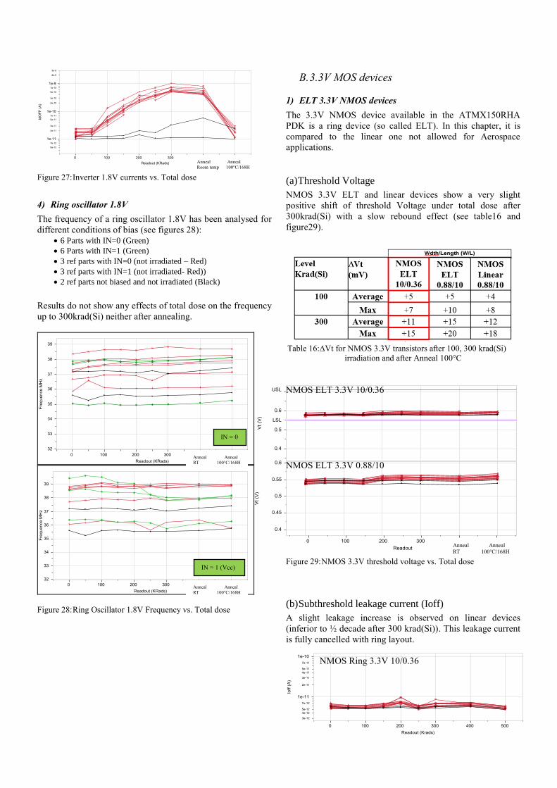
Figure 27: Inverter 1.8V currents vs. Total dose
4) Ring oscillator 1.8V
The frequency of a ring oscillator 1.8V has been analysed for
different conditions of bias (see figures 28): • 6 Parts with IN=0 (Green)
• 6 Parts with IN=1 (Green)
• 3 ref parts with IN=0 (not irradiated – Red)
• 3 ref parts with IN=1 (not irradiated- Red))
• 2 ref parts not biased and not irradiated (Black)
Results do not show any effects of total dose on the frequency
up to 300krad(Si) neither after annealing.
Figure 28: Ring Oscillator 1.8V Frequency vs. Total dose
B. 3.3V MOS devices
1) ELT 3.3V NMOS devices
The 3.3V NMOS device available in the ATMX150RHA
PDK is a ring device (so called ELT). In this chapter, it is
compared to the linear one not allowed for Aerospace
applications.
(a) Threshold Voltage
NMOS 3.3V ELT and linear devices show a very slight
positive shift of threshold Voltage under total dose after
300krad(Si) with a slow rebound effect (see table16 and
figure29).
Table 16: Vt for NMOS 3.3V transistors after 100, 300 krad(Si)
irradiation and after Anneal 100°C
NMOS ELT 3.3V 10/0.36
NMOS ELT 3.3V 0.88/10
Figure 29: NMOS 3.3V threshold voltage vs. Total dose
(b) Subthreshold leakage current (Ioff)
A slight leakage increase is observed on linear devices
(inferior to ½ decade after 300 krad(Si)). This leakage current
is fully cancelled with ring layout.
NMOS Ring 3.3V 10/0.36
Anneal Anneal
RT 100°C/168H
Anneal Anneal
Room temp 100°C/168H
IN = 0
IN = 1 (Vcc)
Anneal Anneal
RT 100°C/168H
Anneal Anneal
RT 100°C/168H
NMOS Ring 3.3V 0.88/10
Figure 30: NMOS 3.3V ELT Subthreshold current vs. Total dose
(c) Input/Output characteristics of NMOS 3.3V
For each 3.3V NMOS devices studied versus the total dose,
the output and input I(V) curves are measured.
For all graphs:
• Blue for the curves before irradiation, red for the curves
at 100 krad(Si), Green for the curves at 300 krad(Si)
• Id(Vg) for Vd = 0.1V (-0.1V for PMOS)
• Id(Vd) for Vg=Vcc typ (-Vcc typ for PMOS)
The behaviour of NMOS 3.3V with ring layout is very similar
between initial and after 100 and 300 krad(Si) irradiation.
0.00E+00
1.00E-04
2.00E-04
3.00E-04
4.00E-04
5.00E-04
6.00E-04
0 0.3 0.6 0.9 1.2 1.5 1.8 2.1 2.4 2.7 3 3.3
Idra
in
Vg (V)
Id(Vg) NMOS 3.3V 10/0.36 RingVd=0.1V
Id_init
Id_1000Gy
Id_3000Gy
1.00E-12
1.00E-11
1.00E-10
1.00E-09
1.00E-08
1.00E-07
1.00E-06
1.00E-05
1.00E-04
1.00E-03
0 0.3 0.6 0.9 1.2 1.5 1.8 2.1 2.4 2.7 3 3.3
I dra
in (
A)
Vg (V)
Id(Vg) NMOS 3.3V 10/0.36 RingVd=0.1V
Id_init
Id_1000Gy
Id_3000Gy0.00E+00
1.00E-03
2.00E-03
3.00E-03
4.00E-03
5.00E-03
6.00E-03
0 0.3 0.6 0.9 1.2 1.5 1.8 2.1 2.4 2.7 3 3.3
I dra
in (
A)
Vd (V)
Id(Vd) NMOS 3.3V 10/0.36 RingVg = 3.3V
Id_init
Id_1000Gy
Id_3000Gy
Figure 31: Input and Output characteristics for NMOS 3.3V 10/0.36
Ring
The NMOS 3.3V ELT allows to avoid the subthreshold
leakage current which appears usually with the cumulated
dose. The Id(Vg) curve in log scale (figure 32) highlight the
improvement brought by ELT layout compared to linear one.
1.00E-13
1.00E-12
1.00E-11
1.00E-10
1.00E-09
1.00E-08
1.00E-07
1.00E-06
1.00E-05
1.00E-04
0 0.3 0.6 0.9 1.2 1.5 1.8 2.1 2.4 2.7 3 3.3
I dra
in (
A)
Vg (V)
Id(Vg) NMOS 3.3V 0.88/10 LinearVd=0.1V
Id_init
Id_1000Gy
Id_3000Gy
1.00E-13
1.00E-12
1.00E-11
1.00E-10
1.00E-09
1.00E-08
1.00E-07
1.00E-06
1.00E-05
1.00E-04
0 0.3 0.6 0.9 1.2 1.5 1.8 2.1 2.4 2.7 3 3.3
I dra
in (
A)
Vg (V)
Id(Vg) NMOS 3.3V 0.88/10 RingVd=0.1V
Id_init
Id_1000Gy
Id_3000Gy
Figure 32: ELT effect on subthreshold leakage current on NMOS
3.3V (top: linear devices, bottom: ELT devices)
2) PMOS 3.3V devices
For each 3.3V PMOS devices studied versus the total dose,
the output and input I(V) curves are measured.
(a) Input/Output characteristics of PMOS 3.3V
In the same way as PMOS 1.8V, the electrical characteristics
of PMOS 3.3V devices do not show any difference after
irradiation.
0
0.000025
0.00005
0.000075
0.0001
0.000125
0.00015
0.000175
0.0002
0.000225
0 0.3 0.6 0.9 1.2 1.5 1.8 2.1 2.4 2.7 3 3.3
Idra
in (A
)
Vg (V)
Id(Vg) PMOS 3.3V 10/0.36 LinearVd=0.1V
Id_init
Id_1000Gy
Id_3000Gy
1E-12
1E-11
1E-10
1E-09
1E-08
0.0000001
0.000001
0.00001
0.0001
0.001
0 0.3 0.6 0.9 1.2 1.5 1.8 2.1 2.4 2.7 3 3.3
I dra
in (
A)
Vg (V)
Id(Vg) PMOS 3.3V 10/0.36 LinearVd=0.1V
Id_init
Id_1000Gy
Id_3000Gy0
0.0005
0.001
0.0015
0.002
0.0025
0.003
0 0.3 0.6 0.9 1.2 1.5 1.8 2.1 2.4 2.7 3 3.3
I dra
in (
A)
Vd (V)
Id(Vd) PMOS 3.3V 10/0.36 LinearVg = 3.3V
Id_init
Id_1000Gy
Id_3000Gy
Figure 33: In and Output characteristics for PMOS 3.3V 10/0.36
Anneal Anneal
RT 100°C/168H
C. 5V MOS devices
1) 5V NMOS devices
(a) Threshold Voltage
As expected by theory and because the 5V devices are
processed with a 250Å-oxide (commonly used for 15V
devices), this device is influenced by the cumulated dose. This
drift on Vth depends mainly of:
• the oxide thickness
• the electrical field in the oxide during irradiation
It is commonly expected to have more than 400 mV /
100krad(Si) of drift on Vt Nmos with a maximum electrical
field (Vcc max = 15V) on this oxide thickness. For the Nmos
5V using the 250Å oxide this drift is reduced due to the
voltage limitation of Vcc max = 5.5V.
According to the theory and the experiments this drift is
inferior to 40mV/100 krad(Si) for the short device and close
to 110mV/100 krad(Si) for the narrowest one.
The ELT does not enable to reduce this Vth drift (fig. 34).
This result shows that this effect is a mainly active area effect;
not due to the parasitic devices along the trench edge.
Figure 34: Nmos 5V – ELT 20/1: Vt drift (V) vs Dose (krad(Si))
(b) Subthreshold leakage current
In contrast with what we explained about the Vth, the ring
layout reduced drastically the leakage current effect brought
by the parasitic transistor (fig. 35).
Figure 35: Nmos 5V – 20/1 short device: Subthreshold leakage (A)
current vs Dose (krad(Si)) - top: linear, bottom: ELT
Ring layout has a major effect on leakage current with a large
reduction observed of 4 decades with ring layout at 100 and
300 krads(Si).
The leakage current fully recovers after annealing but rebound
effect is noticed on threshold Voltage (Vth) on both layout.
The ELT remains mandatory to reduce drastically leakage
current.
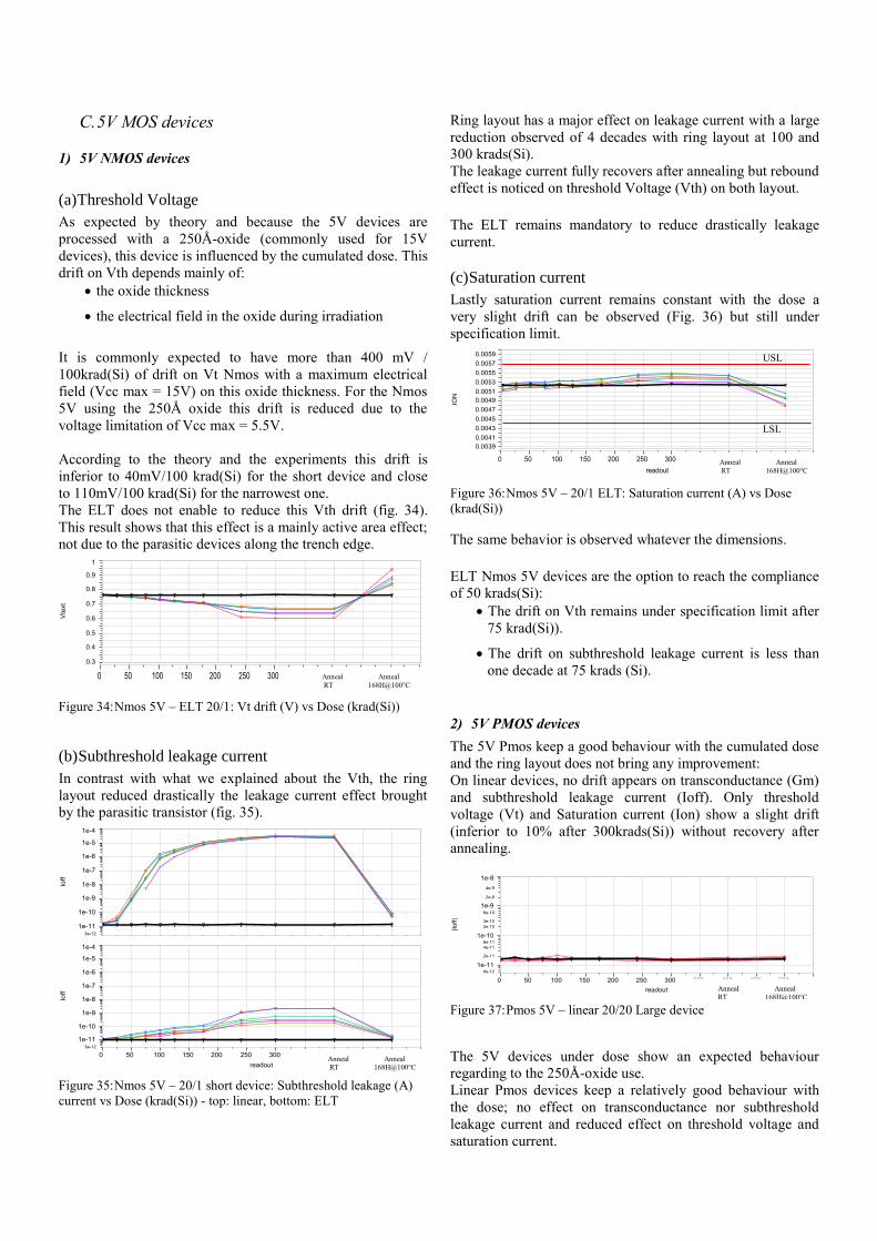
(c) Saturation current
Lastly saturation current remains constant with the dose a
very slight drift can be observed (Fig. 36) but still under
specification limit.
Figure 36: Nmos 5V – 20/1 ELT: Saturation current (A) vs Dose
(krad(Si))
The same behavior is observed whatever the dimensions.
ELT Nmos 5V devices are the option to reach the compliance
of 50 krads(Si):
• The drift on Vth remains under specification limit after
75 krad(Si)).
• The drift on subthreshold leakage current is less than
one decade at 75 krads (Si).
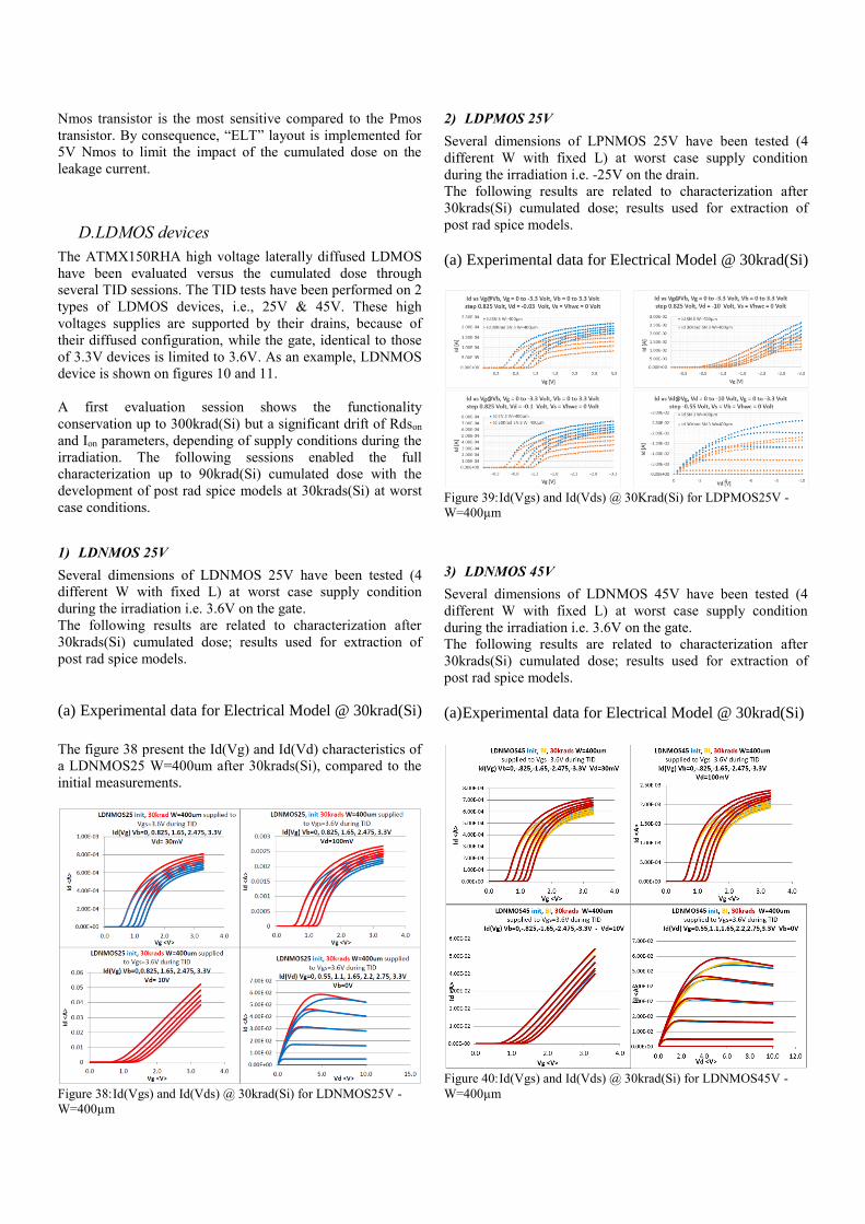
2) 5V PMOS devices
The 5V Pmos keep a good behaviour with the cumulated dose
and the ring layout does not bring any improvement:
On linear devices, no drift appears on transconductance (Gm)
and subthreshold leakage current (Ioff). Only threshold
voltage (Vt) and Saturation current (Ion) show a slight drift
(inferior to 10% after 300krads(Si)) without recovery after
annealing.
Figure 37: Pmos 5V – linear 20/20 Large device
The 5V devices under dose show an expected behaviour
regarding to the 250Å-oxide use.
Linear Pmos devices keep a relatively good behaviour with
the dose; no effect on transconductance nor subthreshold
leakage current and reduced effect on threshold voltage and
saturation current.
USL
LSL
Anneal Anneal
RT 168H@100°C
Anneal Anneal
RT 168H@100°C
Anneal Anneal RT 168H@100°C
Anneal Anneal
RT 168H@100°C
Nmos transistor is the most sensitive compared to the Pmos
transistor. By consequence, “ELT” layout is implemented for
5V Nmos to limit the impact of the cumulated dose on the
leakage current.
D. LDMOS devices
The ATMX150RHA high voltage laterally diffused LDMOS
have been evaluated versus the cumulated dose through
several TID sessions. The TID tests have been performed on 2
types of LDMOS devices, i.e., 25V & 45V. These high
voltages supplies are supported by their drains, because of
their diffused configuration, while the gate, identical to those
of 3.3V devices is limited to 3.6V. As an example, LDNMOS
device is shown on figures 10 and 11.
A first evaluation session shows the functionality
conservation up to 300krad(Si) but a significant drift of Rdson
and Ion parameters, depending of supply conditions during the
irradiation. The following sessions enabled the full
characterization up to 90krad(Si) cumulated dose with the
development of post rad spice models at 30krads(Si) at worst
case conditions.
1) LDNMOS 25V
Several dimensions of LDNMOS 25V have been tested (4
different W with fixed L) at worst case supply condition
during the irradiation i.e. 3.6V on the gate.
The following results are related to characterization after
30krads(Si) cumulated dose; results used for extraction of
post rad spice models.
(a) Experimental data for Electrical Model @ 30krad(Si)
The figure 38 present the Id(Vg) and Id(Vd) characteristics of
a LDNMOS25 W=400um after 30krads(Si), compared to the
initial measurements.
Figure 38: Id(Vgs) and Id(Vds) @ 30krad(Si) for LDNMOS25V -
W=400µm
2) LDPMOS 25V
Several dimensions of LPNMOS 25V have been tested (4
different W with fixed L) at worst case supply condition
during the irradiation i.e. -25V on the drain.
The following results are related to characterization after
30krads(Si) cumulated dose; results used for extraction of
post rad spice models.
(a) Experimental data for Electrical Model @ 30krad(Si)
Figure 39: Id(Vgs) and Id(Vds) @ 30Krad(Si) for LDPMOS25V -
W=400µm
3) LDNMOS 45V
Several dimensions of LDNMOS 45V have been tested (4
different W with fixed L) at worst case supply condition
during the irradiation i.e. 3.6V on the gate.
The following results are related to characterization after
30krads(Si) cumulated dose; results used for extraction of
post rad spice models.
(a) Experimental data for Electrical Model @ 30krad(Si)
Figure 40: Id(Vgs) and Id(Vds) @ 30krad(Si) for LDNMOS45V -
W=400µm
4) LDPMOS 45V
Several dimensions of LDPMOS 45V have been tested (4
different W with fixed L) at worst case supply condition
during the irradiation i.e. -45V on the drain.
The following results are related to characterization after
30krads(Si) cumulated dose; results used for extraction of
post rad spice models.
(a) Experimental data for Electrical Model @ 30krad(Si)
Figure 41: Id(Vgs) and Id(Vds) @ 30krad(Si) for LDNMOS45V -
W=400µm
VII. CONCLUSION
The ATMX150RHA has been tested according to
JESD57/ESCC25100 and to 1019.5 MIL STD 883 test
method.
The digital ATMX150RHA test vehicle has been tested
successfully up to a total dose of 300 krad(Si), without
rebound effect.
Different evaluations at device level have been done showing
the TID capability of the technology for the different domain
of the devices.
The heavy ions SEE test results have demonstrated the large
capability of the ATMX150RHA:
• the latch-up immunity of the ATMX150RHA ASIC
family at maximum temperature (threshold LET higher
than 78 MeV/mg/cm2).
• the efficiency of the SEU hardening techniques used for
ATMX150RHA SEU hardened DFF (a LET threshold
upper than 18.5 MeV/mg/cm2)
• the very good SEU hardening results obtained for the
compiled memories when used with error correction
code.
• the sensitivity of the standard DFF to SEU (LET
threshold of 3.0 MeV/mg/cm2).
• No SEU event was observed in any run with TMR
hardening.
• No SEB on LDMOS 25 and 45V
• No SEGR on LDPMOS 25 and 45V and SOA on
LDNMOS
Based on these results the ATMX150RHA features meet the
radiation performance required for space applications.
VIII. REFERENCES
[1] E.Leduc. (2012, Nov). L2.4a rapport de caractérisation de la
technologie sous Total Dose.
CNES CONTRACT n° 4500037909 / DCT094 of 2011.09.27
[2] E.Leduc. (2013, Mar). L2.4g: Rapport d’évaluation TID et SEE
du vehicule de test V54.
CNES CONTRACT n° 4500037909 / DCT094 of 2011.09.27
[3] E.Leduc. (2014, Jul). Radiation evaluation on MOS 5V devices
(Cumulated dose) – AT77K
CNES CONTRACT n° 4500044431 / DCT094 of 2013.10.24
[4] D.Truyen. (2015, Feb). 02FU (UMC Foundry) – AT77KRHA
Test Vehicle - Single Event Effects Report
CNES CONTRACT n° 4500037909 / DCT094 of 2011.09.27
[5] S.Furic. (2017, Feb). L1.2-Rapport d’évaluation Hautes
Tensions LDMOS 25V, 45V et 65V sous TID.
CNES CONTRACT n° 4500044431 / DCT094 of 2013.10.24
[6] S.Furic, D.Truyen. (2017, Nov). L2.2-Rapport d’évaluation
SEE des dispositifs Hautes Tensions LDMOS 25V, 45V et 65V.
CNES CONTRACT n° 4500044431 / DCT094 of 2013.10.24
[7] S.Furic. (2017, Nov). L1 : Rapport d'intégration dans les
modèles SPICE (TID LDMOS)
CNES CONTRACT n° 4500053131 / DCT094 of 26.08.2016