Embed Size (px)
Citation preview
A CALIFORNIA MICRO DEVICES G65SC151
MicrocircuitsADV-CMOS Communications Terminal Unit (Telecommunication Microcomputer)Features• Standard Option to the G65SC150 Communications Terminal
Unit (CTU)• Generates signals compatible with switched telephone
networks or packet switched data networks• Provides Dial Pulse (DP), Dual Tone Multi-Frequency
(DTMF), and 0-600 baud modem signaling capabilities• Low power mode (300 *iA) enables telephone line-powered
operation• External microprocessor address and data bus facilitates
memory and I/O expansion• On-chip memory: 64 bytes RAM, with facilities for external
ROM or EPROM• Standard DTMF and modem frequencies can be generated
which are accurate to ±1.0% with a 3.58 MHz crystal■ Two sine wave generators• 6800 and 6500 bus compatibility• Utilizes G65SC00 microprocessor as CPU• 27 TTL compatible I/O lines• Bus expandable to address 65K bytes of external memory• Single +5 volt power supply• Available in 68-pin chip carriers
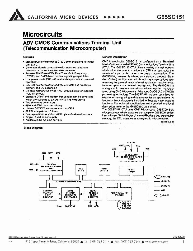
General DescriptionCMD Microcircuits' G65SC151 is configured as a Standard Mask Option to the G65SC150 Communications Terminal Unit (CTU). The G65SC150 CTU offers a variety of mask options which allow the user to configure a CTU that best suits the needs of a particular or unique design application. The G65SC151, however, is offered as a standard product (Standard Option) configuration which includes those options representing the general needs of most application requirements. Included options are detailed on page two. The G65SC151 is a single chip telecommunications microcomputer manufactured using CMD Microcircuits’ Advanced CMOS (ADV-CMOS) processing technology. The G65SC151 has been optimized for telephone line signaling and data transmission applications. A functional block diagram is included to illustrate major system functions. For technical specifications and a detailed functional description, refer to the G65SC150 data sheet.The G65SC151 CTU uses CMD Microcircuits' G65SC00 8-bit microprocessor which executes the complete G65SC00 series instruction set. With 64 bytes of internal RAM and bus expandable memory, the CTU operates as a single-chip microcomputer.
(cont inued)
Block Diagram
BE-
RbV-
n m i moi moo
t I *
□ADDRESS AND DATA BUS
CLK(IN)
OSC(OUT) I Vs*
RESuG65SC00
m ic r o p r o c e s s o rAND RAM ROM
CONTROL REGISTER 64 - a 2048 - 8
:< o u t) j
11OSCILLATOR
CLOCK GENERATOR RESET
ri/u
u16-BITTIMER
VflEG TJCC/DTMFT V
RXC ATG
COLUMN/ DUAL ROW/TRANSMIT 26-STEP RECEIVE PERIPHERAL I/O
8-BIT SINE WAVE 16-BIT 27 LINESCOUNTER GENERATOR COUNTER
A0-A15
— *2 (OUT)
— *4 (OUT)
— R/W
D0-D7
© 2000 Californ ia Micro Devices Corp. All rights reserved. C1040500
s/oo 21 5 Topaz Street, Milpitas, California 95035 A Tel: (408) 263-3214 A Fax: (408) 26 3 -7846 A www.calmicro.com 1
A CALIFORNIA MICRO DEVICES G65SC151
The CTU's internal bus interconnects all microcomputer functions. The address and data bus buffers permit expansion for the addition of ROM, RAM and memory mapped I/O using the full 65K addressing space of the microprocessor. A peripheral mode is available for use with multiprocessor systems. The on-chip oscillator may be driven by an external clock source.The telecommunications interface circuitry consists of a timer, row/receive counter, column/transmit counter and dual sine wave generators. In addition, 27 general purpose I/O lines can be used for Keyboard, telephone Dial Pulse (DP) signaling, phone line control, and other peripheral devices.
Standard OptionsThe following Standard Options have been implemented within the G65SC151 CTU. Note that the G65SC151 is identical to the G65SC150 CTU in technical specifications and functional operation. Refer to the G65SC150 CTU data sheet for detailed specifications and operation.
1. The oscillator feedback resistor (between CLK (IN) and OSC (OUT)) is not provided.
2. The following control signals are provided with pull-up resistors at 20 nk pull-up current:BE NMIIRQO RDYIRQ1 RES
3. Pin 51 is provided with the Port D signal PD2.
4. Pin 59 (Vreg) requires an external connection toVDD.
5. The following I/O source currents are provided:PA0-PA7 200 mA pull-up PD0-PD2 1 mA pull-upPB0-PB7 200 ^A pull-up ATG 10 jiA pull-upPC0-PC7 no pull-up
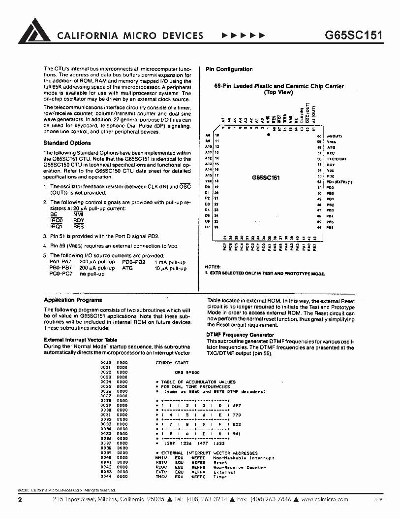
Pin Configuration
68-Pin Leaded Plastic and Ceramic Chip Carrier (Top View)
t- w t n v n w —2 0 3
O
A« 10A9 11
A10 12
A11 13
A12 14A13 ISA14 It
A15 17
V U 1»
DO 19
D1 20D2 21
D3 22
D4 23
OS 24
Dt 2507 2t
G65SC151
M *4(OUT)
59 Vreg
sa ATG
57 RXC
56 TXC/DTMF
55 HOY
54 VOD
53 PD052 PD1 <EXT»D<1)51 PD2
50 PB049 PB1
40 PB247 PB3
46 PB4
45 PB544 PBS
a s s w w n w « * * ^ Jr» « m * n n ^ o K« « < < < < < < ma & & a- o. a. b a a .
NOTES:1. EXTR SELECTED ONLY IN TEST AND PROTOTYPE MODE.
Application Programs
The following program consists of two subroutines which will be of value in G65SC151 applications. Note that these subroutines will be included in internal ROM on future devices. These subroutines include:
External Interrupt Vector TableDuring the “Normal Mode" startup sequence, this subroutine automatically directs the microprocessor to an Interrupt Vector
Table located in external ROM, In this way, the external Reset circuit is no longer required to initiate the Test and Prototype Mode in order to access external ROM. The Reset circuit can now perform the normal reset function, thus greatly simplifying the Reset circuit requirement.
DTMF Frequency GeneratorThis subroutine generates DTMF frequencies for various oscillator frequencies. The DTMF frequencies are presented at the TXC/DTMF output (pin 56).
00200021002200230024 00 25 0026 0 0 2 ? 0028 0029 00 3000310032003300340035003 600370038003900400041004200430044
0000000000000000000000000000000000000000000000000000000000000000000000000000oooo00000000000000000000
CTUROM START
ORG *FE00
* TABLE OF ACCUMULATOR VALUES* FOR DUAL TONE FREQUENCIES* (same *s 8840 *nd 8870 DTMF d f c o d e r s )
I I I 1 D I 697 »♦— - - - ♦
1 E 1 770* I 4 I 5 I* ♦ ------------+ — - —* I 7 I 8 I 9 1 F I 852* 4 ------------1.+------------- +
* 1 B I A I C I 0 1 941
* 1209 1336 1477 1633
* EXTERNAL INTERRUPT SECTOR ADDRESSESNMI U EQU *EFEC N o n - M * * k * b l # I n t e r r u p tRSTV EQU ♦EFEE R * * * tRCW EQU ♦EFF8 R o w -R » c * iv t C ounterEXTV EQU *EFFA Ex t e r n * lTMCV EQU ♦EFFC T i m*r
© 2000 Californ ia Micro Devices Corp. All rights reserved.
2 21 5 Topaz Street, Milpitas, California 95035 A Tel: (408) 263-321 4 A Fax: (408) 26 3 -7846 A www.calmicro.com 5/oo
A CALIFORNIA MICRO DEVICES
004500440 0 4 ?00400049005000510052005300540 055005600570058 005? 0040 0061 0062006300640 0 6 5006600670068006900700071007200730074007500760077007800790080 0081 0082008300840085008600870088008900900091009200930094009500960097009800990100 0 1 0 1 0 1 0 201030104010501060107010801090110 0111 0 1 1 2 011301 14 0115 01 16 0117 01 18 01 19 0 120 0121 01 22012301240125 01 26 0127 01 28012901300131
o o o o000000000000oooo0000o o o oooooo o o oo o o oo o o oo o o oo o o oo o o o0004 0008 o o o c 0010 0010 0014 0018 001C 0020 0020 0024 0028 002C 0030 0030 0034 0038 003C 0040 0040 0040 0040 0044 0048 004C 0050 0050 0054 0058 005C 0060 0060 0064 0068 006C 0070 0070 0074 0078 007C 0080 0080 0080 0080 0083 0086 0088 0088 0060 008E 0090 0090 0093 0096 0098 0098 0098 009E 009E OOAO 00*2 00A3 00A3 OOA3 OOA5 00A7 00A9 OOAB 00 AD OOAE OOAE OOAE 00B1
BRKV EQU SEFFE Break I n s t r u c t i o n
* CTU ON-CHIP I / O ADDRESSES ROW EQU *F 4 Row-Receive C ou n te rCOL EQU * F 6 Col omn-Transim t C oun terCNTRL EQU SF7 C o n t r o l - S t a t u s R e g i s t e r
E x t e r n a l But T h r e e - S t a t e C o n tro DTMF Mode
486262585858505048486258
516D6D636363595951516D63
7AA5A595959586867A7AA595
A2DCDC C7C7C7 B4B4A2 A2DCC7
29383338332E332E332E2929
2E3F393F3933393339332E2E
465E555E554D554D554D4646
5D7E727E7267726772675D5D
BD3000BC70008016
BD2000BC6000BOOE
BD10008C50008006
BDOOOOBC4000
* CONSTANTSTSC EQU *2 0DTMF EQU * 0 7
EJECT* DTMF VALUES FOR ROU-RECEIVE COUNTER
R358
R60
DC t 1 ‘•7 2 , 9 8 , 9 8 , 9 8 ' 3 . 58 MHzDC I 1 ' 88. 8 8 ,8 8 , 8 0 'DC 11 ■'80 * 8 0 , 7 2DC I 1''7 2 , 9 8 ,8 8 ,8 0 '
DC I 1 '81 , 109, 10 9 , 109- 4 .0 MHiDC I 1 ■' 9 9 , 9 9 , 9 9 , 8 9 'DC I 1 ' 8 9 , 89 ,81 ,81 'DC I 1 ' 8 1 , 1 0 9 , 9 9 , 8 9 '
DC I 1 '12 2 .1 6 5 . 1 65, 165' 6. 0 MHzDC I 1 '14 9 t 149, 149 , 134 'DC I 1 ■'134 ♦ 134, 122, 122'DC I 1 '12 2 ,1 6 5 , 1 4 9 , 134'
DC I 1 '1 6 2 ,2 2 0 , 2 2 0 . 220 ' ’ 8 . 0 MH?DC I 1 '19 9 .1 9 9 . 199 . 180'DC 11 ' 180 ,1 8 0 , 162, 162'DC I 1 ' 162 .2 2 0 , 199 , 180'
* DTMF V a lu e s -for Column D i v i d e r
C358
C40
C60
DCDCDCDC
DCDCDCDC
DCDCDCDC
1 3 ' 4 1 , 5 6 , 5 1 , 4 6 ' I 1 ' 5 6 , 5 1 , 4 6 , 5 6 ' I 1 ' 5 1 , 4 6 , 5 1 , 5 6 ' I I ' 4 6 , 4 1 , 4 1 , 4 1 '1 1 ' 4 6 , 6 3 , 5 7 , 5 1 ' 1 1 ' 6 3 , 5 7 , 5 1 , 6 3 ' I 1 ' 5 7 , 5 1 , 5 7 , 6 3 ' 1 1 ' 5 1 , 4 6 , 4 6 , 4 6 'I I ' 7 0 , 9 4 , 8 5 , 7 7 ' I I ' 9 4 , 8 5 , 7 7 , 9 4 ' I 1 ' 8 5 , 7 7 , 8 5 , 9 4 ' I 1 ' 7 7 , 7 0 , 7 0 , 7 0 '
3 , 5 8 MHi
6 . 0 MHz
C80 DC DC DC DC EJECT
* S u b ro u t in e lo ad s d
D80
1 1 ' 9 3 , 1 2 6 , 1 1 4 , 1 0 3 'I 1 ' 1 2 6 , L 1 4 , 1 0 3 , 1 2 6 ' I I ' 1 1 4 , 10 3 *1 1 4 , 12 6 ' I 1 ' 1 0 3 , 9 3 , 9 3 , 9 3 '
8 .0 MHz
v i d * r * w i t h DTMF ton e u a lu e s
85F484F660
A90704F764F564F464F660
6CECEF
D40
D358
SEND
DOFF
LDA R80,XLDY C 80,X ,BRA SEND
LDA R60 ,XLDY C60 ,XBRA SEND
LDA R4Q.XLDY C40 ,XBRA SEND
LDA R 358,XLDY C358,X
STA ROUSTY COLRTS
LDATS8ST Z STZ STZ RTS
«DTMF CNTRL ROW* 1 ROU COL
IN IT IA L IZ E TONES OFF
* INTERRUPT VECTOR ROUTINESNMI JMP <NMIV> Non-Maskable
© 2000 Californ ia Micro Devices Corp. All rights reserved.
G65SC151
s/oo 21 5 Topaz Street, Milpitas, California 95035 A Tel: (408) 263-3214 A Fax: (408) 26 3 -7846 A www.calmicro.com 3
A CALIFORNIA MICRO DEVICES G65SC151
0132 00B1 A?20 RST LDA rrsc Reset0133 00B3 85F7 STA CNTRL Set TSC b i t to m b i t0134 00B5 6CEEEF JMP < RSTV) ex t e r n * I bus0135 00880 t 3 6 00B8 6CF8EF RCV JMP (RCW> Row-Rece i ve0137 OOBB 6CFAEF EXT JMP < EXTV) Ex t t r n » l0136 00BE 6CFCEF TMC JMP <TMCV) T t mer0139 00C1 6CFEEF BRK JMP < BRKV) Break I n s t r u c t i o n0140 00C4 EJECT0141 00C4 ORG ♦FF800142 00C40143 00C4 * Set DTMF to n e , o s c i l l a t o r f r e q u e n c y0144 00C4 4CA300 DTMF OF JMP DOFF To nts o f f , and i n i t i a l i z e0145 00C? 4C?800 DTMF35 JMP D358 3 .5 7 ? 5 45 MHz0146 00 CA 4C?000 DTMF40 JMP D40 4 .0 0 00 0 0 MHz0147 00CD 4C8800 DTMF60 JMP D60 6 .000000 MHz0148 OODO 4C8000 DTMF80 JMP D80 8 .0 0 00 0 0 MHZ014? 00D30130 00D3 ORG ♦FFEC01S1 00D30152 00D3 * I n t e r r u p t V e c to r s0153 0003 AE10 DC A ' N I I ' Non-Maskabl e0154 00D5 ei 10 DC A'R ST' Reset0155 00070156 00t>7 ORG *FF F 80157 00D?0158 00D7 B810 DC A'RCV' Row-Rtce tve015? OOD? BB10 DC A'E X T ' Ex t e r n * !0160 00DB BE10 DC A'TMC' T i mer0161 00DD Cl 10 DC A'BRK' Break I n s t r u c t i o n0162 OODF0163 OODF END
Local Symbol T *b 1 e
BRK 00C1 BRKV EFFE C358 0040 C40 0050C60 0060 C80 0070 CNTRL 00F7 COL 00F60358 00?8 D40 00?0 D60 0088 D80 0080DOFF 0QA3 DTMF 0007 DTMF35 OOC7 DTMF40 00CADTMF60 00 CD DTMF80 OODO DTMF OF 00 C4 EXT OOBBEXTV EFFA NMI OOAE hMIV EFEC R358 0000R40 0010 R60 0020 R80 0030 RCV 00B8RCW EFF8 ROU 00F4 RST 00B1 RSTV EFEESEND 00?E TMC OOBE TMCV EFFC TSC 0020
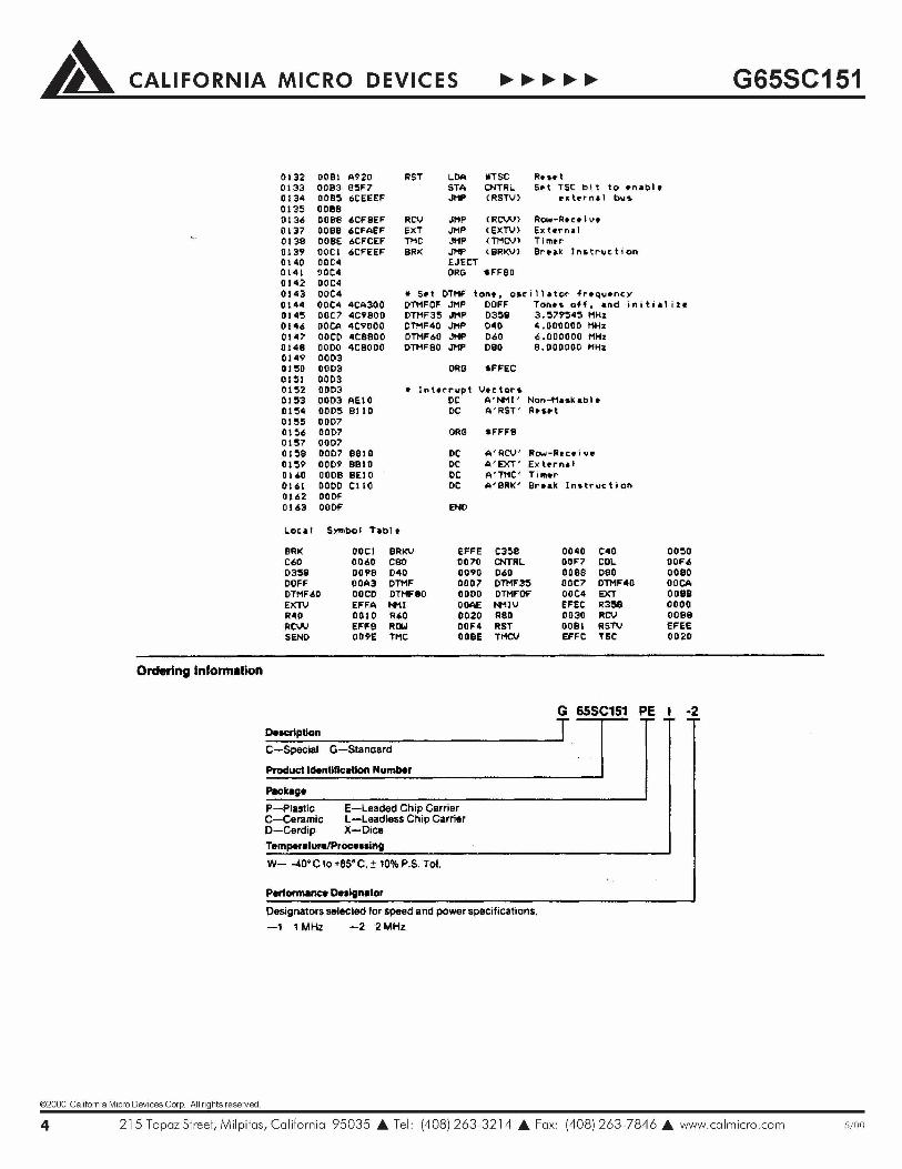
Ordering Information
DescriptionC—Special G—Standard
Product Identification Number
G 6SSC151 PE I
J "-2
PackageP—Plastic E—Leaded Chip CarrierC—Ceramic L—Lead less Chip CarrierD—Cerdip X—DiceTemperature/Processing
W-----10' C to +85' C, ± 10% P.S. Tol.
Performance Designator
Designators selected for speed and power specifications. —1 1 MHz —2 2 MHz
© 2000 Californ ia Micro Devices Corp. All rights reserved.
4 21 5 Topaz Street, Milpitas, California 95035 A Tel: (408) 263-321 4 A Fax: (408) 26 3 -7846 A www.calmicro.com 5/oo