Embed Size (px)
Citation preview
Data Sheet 08.95
Microcomputer Components
SAB 80515 / SAB 80535
8-Bit Single-Chip Microcontroller Family
SAB 80515 / 80535 Data SheetRevision History: Current Version: 08.95
Previous Version: 09.89, 11.92
Page Subjects (changes since last revision)
1, 2, 27,29, 302936
– 40 to + 110 ˚C version deleted; Note: only on request ... added
tC and Vint ERROR modifiedHeader of table (16 MHz) corrected
Edition 08.95
This edition was realized using the software system FrameMaker.
Published by Siemens AG,Bereich Halbleiter, Marketing-Kommunikation, Balanstraße 73,81541 München© Siemens AG 1995.All Rights Reserved.
Attention please!
As far as patents or other rights of third parties are concerned, liability is only assumed for components, not for applications, processes andcircuits implemented within components or assemblies.
The information describes the type of component and shall not be considered as assured characteristics.
Terms of delivery and rights to change design reserved.
For questions on technology, delivery and prices please contact the Semiconductor Group Offices in Germany or the Siemens Companies andRepresentatives worldwide (see address list).
Due to technical requirements components may contain dangerous substances. For information on the types in question please contact yournearest Siemens Office, Semiconductor Group.
Siemens AG is an approved CECC manufacturer.
Packing
Please use the recycling operators known to you. We can also help you – get in touch with your nearest sales office. By agreement we willtake packing material back, if it is sorted. You must bear the costs of transport.
For packing material that is returned to us unsorted or which we are not obliged to accept, we shall have to invoice you for any costs incurred.
Components used in life-support devices or systems must be expressly authorized for such purpose!
Critical components1 of the Semiconductor Group of Siemens AG, may only be used in life-support devices or systems2 with the express writ-ten approval of the Semiconductor Group of Siemens AG.
1 A critical component is a component used in a life-support device or system whose failure can reasonably be expected to cause the failureof that life-support device or system, or to affect its safety or effectiveness of that device or system.
2 Life support devices or systems are intended (a) to be implanted in the human body, or (b) to support and/or maintain and sustain humanlife. If they fail, it is reasonable to assume that the health of the user may be endangered.
Semiconductor Group 3 8.95
High-Performance8-Bit Single Chip Microcontroller SAB 80515/80535
Preliminary
SAB 80515 Microcontroller with factory mask-programmable ROMSAB 80535 Microcontroller for external ROM
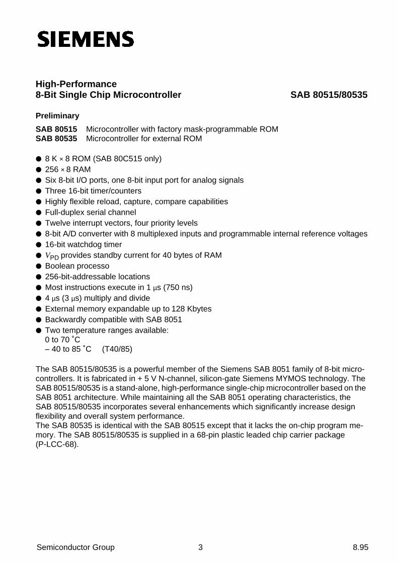
8 K × 8 ROM (SAB 80C515 only) 256 × 8 RAM Six 8-bit I/O ports, one 8-bit input port for analog signals Three 16-bit timer/counters Highly flexible reload, capture, compare capabilities Full-duplex serial channel Twelve interrupt vectors, four priority levels 8-bit A/D converter with 8 multiplexed inputs and programmable internal reference voltages 16-bit watchdog timer VPD provides standby current for 40 bytes of RAM Boolean processo 256-bit-addressable locations Most instructions execute in 1 µs (750 ns) 4 µs (3 µs) multiply and divide External memory expandable up to 128 Kbytes Backwardly compatible with SAB 8051 Two temperature ranges available:
0 to 70 ˚C– 40 to 85 ˚C (T40/85)
The SAB 80515/80535 is a powerful member of the Siemens SAB 8051 family of 8-bit micro-controllers. It is fabricated in + 5 V N-channel, silicon-gate Siemens MYMOS technology. TheSAB 80515/80535 is a stand-alone, high-performance single-chip microcontroller based on theSAB 8051 architecture. While maintaining all the SAB 8051 operating characteristics, theSAB 80515/80535 incorporates several enhancements which significantly increase designflexibility and overall system performance.The SAB 80535 is identical with the SAB 80515 except that it lacks the on-chip program me-mory. The SAB 80515/80535 is supplied in a 68-pin plastic leaded chip carrier package(P-LCC-68).
SAB 80515/80535
Semiconductor Group 4
Note: Extended temperature range – 40 to 110 ˚C on request
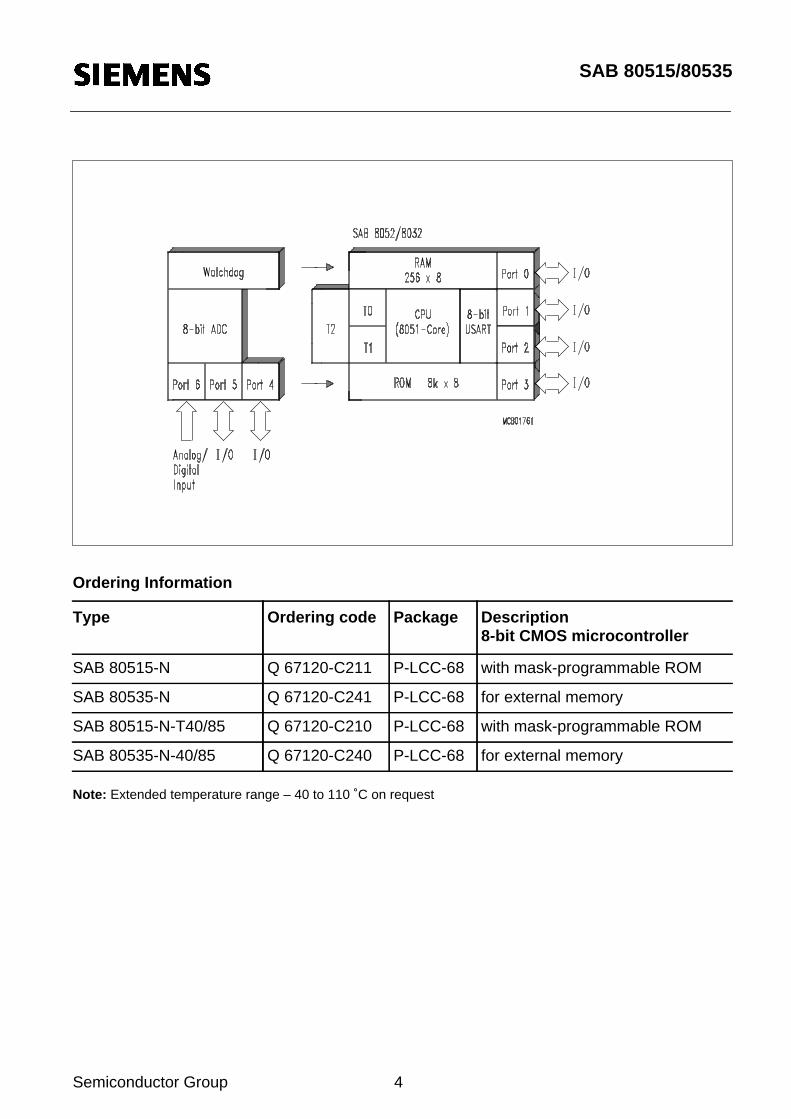
Ordering Information
Type Ordering code Package Description8-bit CMOS microcontroller
SAB 80515-N Q 67120-C211 P-LCC-68 with mask-programmable ROM
SAB 80535-N Q 67120-C241 P-LCC-68 for external memory
SAB 80515-N-T40/85 Q 67120-C210 P-LCC-68 with mask-programmable ROM
SAB 80535-N-40/85 Q 67120-C240 P-LCC-68 for external memory
SAB 80515/80535
Semiconductor Group 5
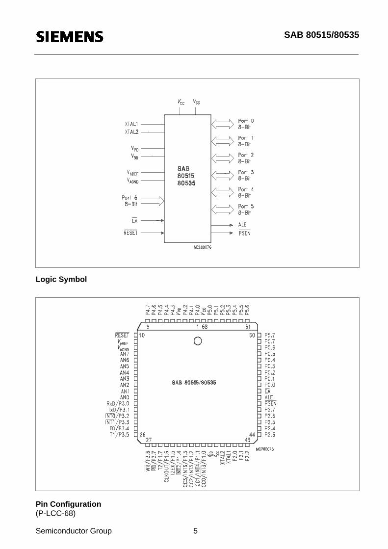
Logic Symbol
Pin Configuration(P-LCC-68)
SAB 80515/80535
Semiconductor Group 6
Pin Definitions and Functions
Symbol Pin Input (I)Output (O)
Function
P4.0-P4.7 1-3, 5-9 I/O Port 4is an 8-bit quasi-bidirectional I/O port .Port 4 can sink/source 4 LS-TTL loads.
VPD 4 I Power down supply. If VPD is held within its specs whileVCC drops below specs,VPD will provide standby powerto 40 byte of the internal RAM. WhenVPD is low, theRAM’s current is drawn from VCC.
RESET 10 I A low level on this pin for the duration of two machinecycles while the oscillator is running resets theSAB 80C515. A small internal pullup resistor permitspower-on reset using only a capacitor connected toVSS
VAREF 11 Reference voltage for the A/D converter
VAGND 12 Reference ground for the A/D converter
AN7-AN0 13-20 I Multiplexed analog inputs
SAB 80515/80535
Semiconductor Group 7
Pin Definitions and Functions (cont’d)
Symbol Pin Input (I)Output (O)
Function
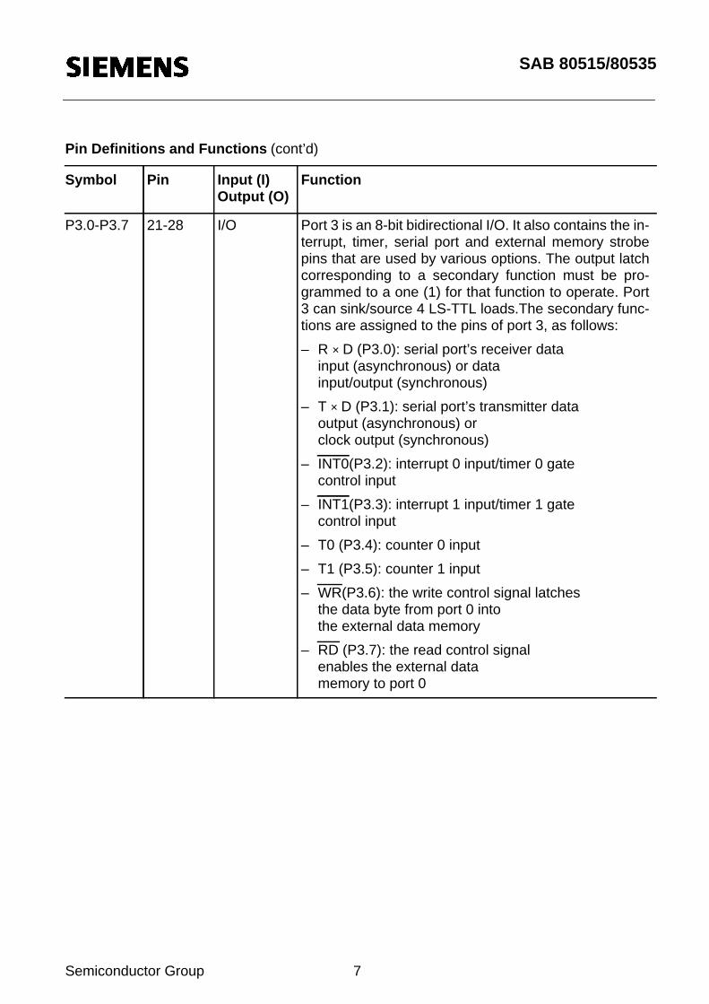
P3.0-P3.7 21-28 I/O Port 3 is an 8-bit bidirectional I/O. It also contains the in-terrupt, timer, serial port and external memory strobepins that are used by various options. The output latchcorresponding to a secondary function must be pro-grammed to a one (1) for that function to operate. Port3 can sink/source 4 LS-TTL loads.The secondary func-tions are assigned to the pins of port 3, as follows:
– R × D (P3.0): serial port’s receiver datainput (asynchronous) or datainput/output (synchronous)
– T × D (P3.1): serial port’s transmitter dataoutput (asynchronous) orclock output (synchronous)
– INT0(P3.2): interrupt 0 input/timer 0 gatecontrol input
– INT1(P3.3): interrupt 1 input/timer 1 gatecontrol input
– T0 (P3.4): counter 0 input
– T1 (P3.5): counter 1 input
– WR(P3.6): the write control signal latchesthe data byte from port 0 intothe external data memory
– RD (P3.7): the read control signalenables the external datamemory to port 0
SAB 80515/80535
Semiconductor Group 8
Pin Definitions and Functions (cont’d)
Symbol Pin Input (I)Output (O)
Function
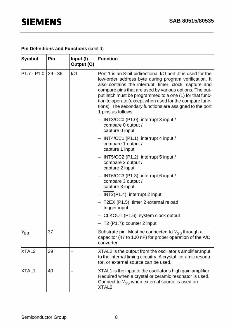
P1.7 - P1.0 29 - 36 I/O Port 1 is an 8-bit bidirectional I/O port .It is used for thelow-order address byte during program verification. Italso contains the interrupt, timer, clock, capture andcompare pins that are used by various options. The out-put latch must be programmed to a one (1) for that func-tion to operate (except when used for the compare func-tions). The secondary functions are assigned to the port1 pins as follows:
– INT3/CC0 (P1.0): interrupt 3 input /compare 0 output /capture 0 input
– INT4/CC1 (P1.1): interrupt 4 input /compare 1 output /capture 1 input
– INT5/CC2 (P1.2): interrupt 5 input /compare 2 output /capture 2 input
– INT6/CC3 (P1.3): interrupt 6 input /compare 3 output /capture 3 input
– INT2(P1.4): interrupt 2 input
– T2EX (P1.5): timer 2 external reloadtrigger input
– CLKOUT (P1.6): system clock output
– T2 (P1.7): counter 2 input
VBB 37 Substrate pin. Must be connected to VSS through acapacitor (47 to 100 nF) for proper operation of the A/Dconverter.
XTAL2 39 – XTAL2 is the output from the oscillator’s amplifier.Inputto the internal timing circuitry. A crystal, ceramic resona-tor, or external source can be used.
XTAL1 40 – XTAL1 is the input to the oscillator’s high gain amplifier.Required when a crystal or ceramic resonator is used.Connect to VSS when external source is used onXTAL2.
SAB 80515/80535
Semiconductor Group 9
Pin Definitions and Functions (cont’d)
Symbol Pin Input (I)Output (O)
Function
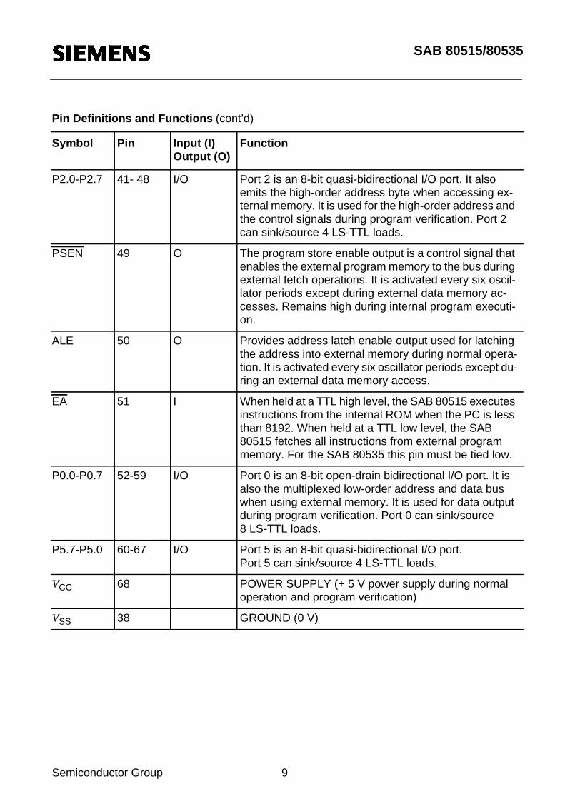
P2.0-P2.7 41- 48 I/O Port 2 is an 8-bit quasi-bidirectional I/O port. It alsoemits the high-order address byte when accessing ex-ternal memory. It is used for the high-order address andthe control signals during program verification. Port 2can sink/source 4 LS-TTL loads.
PSEN 49 O The program store enable output is a control signal thatenables the external program memory to the bus duringexternal fetch operations. It is activated every six oscil-lator periods except during external data memory ac-cesses. Remains high during internal program executi-on.
ALE 50 O Provides address latch enable output used for latchingthe address into external memory during normal opera-tion. It is activated every six oscillator periods except du-ring an external data memory access.
EA 51 I When held at a TTL high level, the SAB 80515 executesinstructions from the internal ROM when the PC is lessthan 8192. When held at a TTL low level, the SAB80515 fetches all instructions from external programmemory. For the SAB 80535 this pin must be tied low.
P0.0-P0.7 52-59 I/O Port 0 is an 8-bit open-drain bidirectional I/O port. It isalso the multiplexed low-order address and data buswhen using external memory. It is used for data outputduring program verification. Port 0 can sink/source8 LS-TTL loads.
P5.7-P5.0 60-67 I/O Port 5 is an 8-bit quasi-bidirectional I/O port.Port 5 can sink/source 4 LS-TTL loads.
VCC 68 POWER SUPPLY (+ 5 V power supply during normaloperation and program verification)
VSS 38 GROUND (0 V)
SAB 80515/80535
Semiconductor Group 10
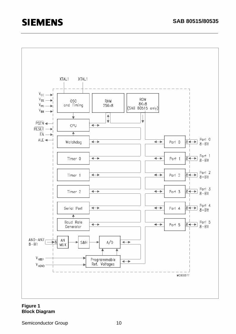
Figure 1Block Diagram
SAB 80515/80535
Semiconductor Group 11
Functional Description
The architecture of the SAB 80515 is based on the SAB 8051 microcontroller family. The fol-lowing features of the SAB 80515 are fully compatible with the SAB 8051 features:
– Instruction set– External memory expansion interface (port 0 and port 2)– Full-duplex serial port– Timer/counter 0 and 1– Alternate functions on port 3– The lower 128 bytes of internal RAM and the lower 4 Kbytes of internal ROM
The SAB 80515 additionally contains 128 bytes of internal RAM and 4 Kbytes of internal ROM,which results in a total of 256 bytes of RAM and 8 Kbytes of ROM on chip. TheSAB 80515 has a new 16-bit timer/counter with a 2:1 prescaler, reload mode, compare andcapture capability. It also contains a 16-bit watchdog timer, an 8-bit A/D converter with pro-grammable reference voltages, two additional quasi-bidirectional 8-bit ports, one 8-bit inputport for analog signals, and a programmable clock output (fOSC/12).Furthermore, the SAB 80515 has a powerful interrupt structure with 12 vectors and 4 program-mable priority levels.Figure 1 shows a block diagram of the SAB 80515.
CPU
The SAB 80515 is efficient both as a controller and as an arithmetic processor. It has extensivefacilities for binary and BCD arithmetic and excels in its bit-handling capabilities. Efficient useof program memory results from an instruction set consisting of 44% one-byte, 41% two-byte,and 15% three-byte instructions. With a 12 MHz crystal, 58% of the instructions execute in1.0 µs.
Memory Organization
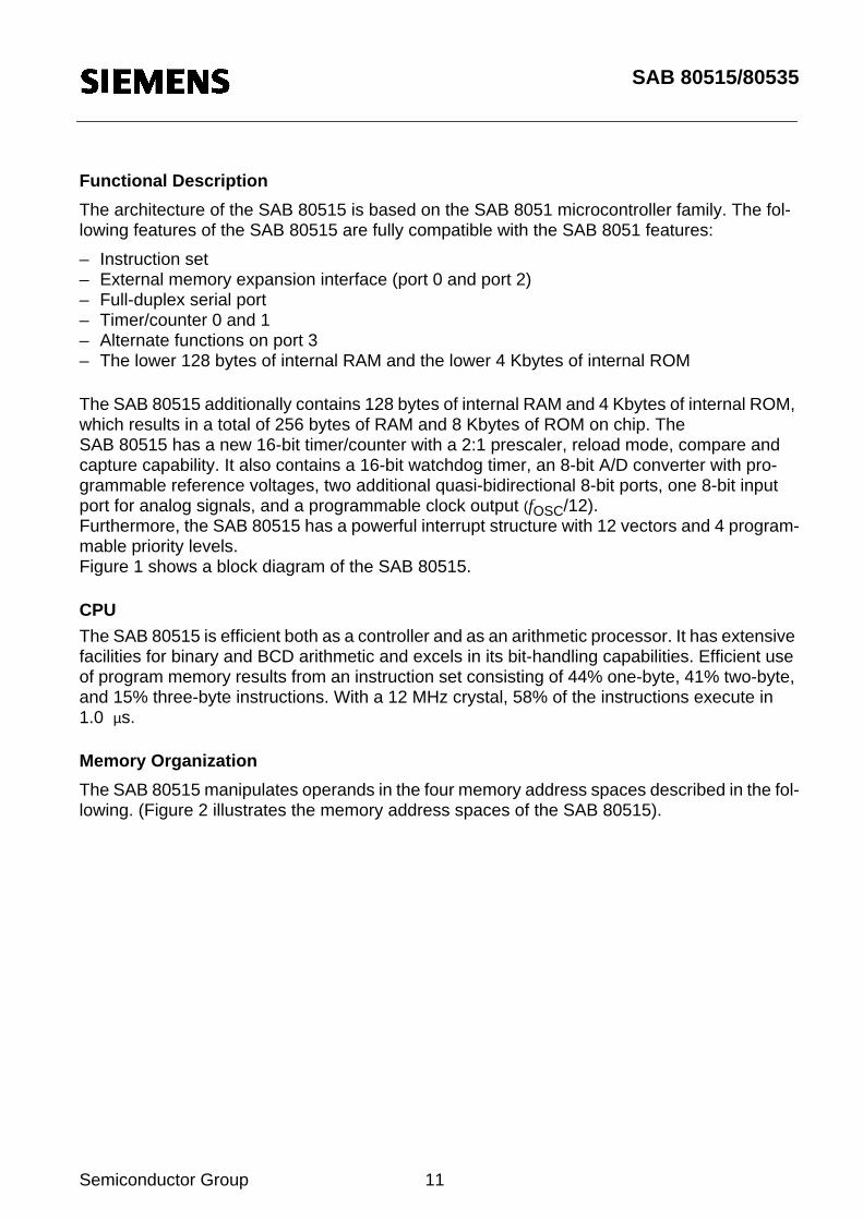
The SAB 80515 manipulates operands in the four memory address spaces described in the fol-lowing. (Figure 2 illustrates the memory address spaces of the SAB 80515).
SAB 80515/80535
Semiconductor Group 12
Figure 2Memory Address Spaces
SAB 80515/80535
Semiconductor Group 13
Program memory
The SAB 80515 has 8 Kbyte of on-chip ROM, while the SAB 80535 has no internal ROM. Theprogram memory can be externally expanded up to 64 Kbytes. If the EA pin is held high, theSAB 80515 executes out of internal ROM unless the address exceeds 1FFFH. Locations 2000Hthrough 0FFFFH are then fetched from the external program memory. If the EA pin is held low,the SAB 80515 fetches all instructions from the external program memory. Since the SAB80535 has no internal ROM, pin EA must be tied low when using this component.
Data Memory
The data memory address space consists of an internal and an external memory space. Theinternal data memory is divided into three physically separate and distinct blocks: the lower 128bytes of RAM, the upper 128 bytes of RAM, and the 128-byte special function register (SFR)area. While the upper 128 bytes of data memory and the SFR area share the same addresslocations, they are accessed through different addressing modes. The lower 128 bytes of datamemory can be accessed through direct or register indirect addressing; the upper 128 bytes ofRAM can be accessed through register indirect addressing; the special function registers areaccessible through direct addressing.Four 8-register banks, each bank consisting of eight 8-bit multi-purpose registers, occupy loca-tions 0 through 1FH in the lower RAM area. The next 16 bytes, locations 20H through 2FH, con-tain 128 directly addressable bit locations. The stack can be located anywhere in the internaldata memory address space, and the stack depth can be expanded up to 256 bytes.The external data memory can be expanded up to 64 Kbytes and can be accessed by instruc-tions that use a 16-bit or an 8-bit address.
SAB 80515/80535
Semiconductor Group 14
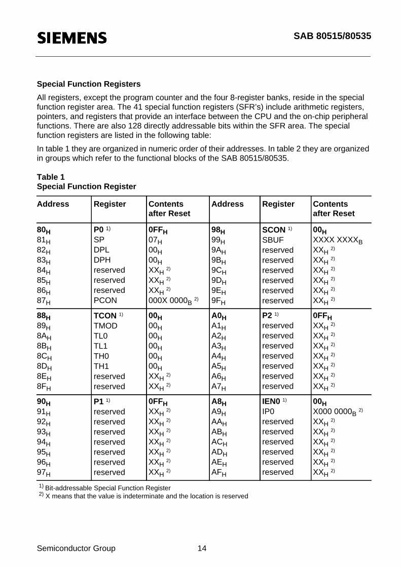
Special Function Registers
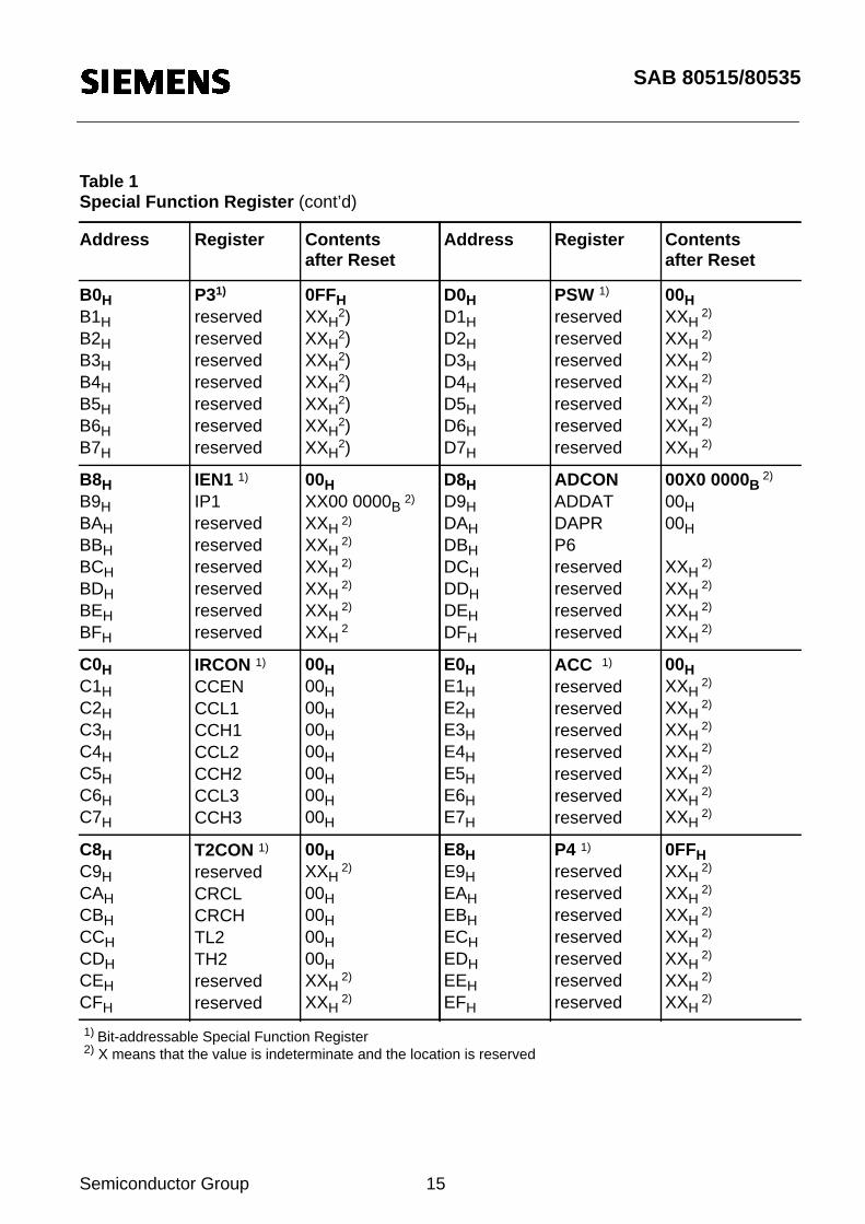
All registers, except the program counter and the four 8-register banks, reside in the specialfunction register area. The 41 special function registers (SFR’s) include arithmetic registers,pointers, and registers that provide an interface between the CPU and the on-chip peripheralfunctions. There are also 128 directly addressable bits within the SFR area. The specialfunction registers are listed in the following table:
In table 1 they are organized in numeric order of their addresses. In table 2 they are organizedin groups which refer to the functional blocks of the SAB 80515/80535.
Table 1Special Function Register
Address Register Contentsafter Reset
Address Register Contentsafter Reset
80H81H82H83H84H85H86H87H
P0 1)
SPDPLDPHreservedreservedreservedPCON
0FFH07H00H00HXXH
2)
XXH2)
XXH2)
000X 0000B2)
98H99H9AH9BH9CH9DH9EH9FH
SCON 1)
SBUFreservedreservedreservedreservedreservedreserved
00HXXXX XXXXBXXH
2)
XXH2)
XXH2)
XXH2)
XXH2)
XXH2)
88H89H8AH8BH8CH8DH8EH8FH
TCON 1)
TMODTL0TL1TH0TH1reservedreserved
00H00H00H00H00H00HXXH
2)
XXH2)
A0HA1HA2HA3HA4HA5HA6HA7H
P2 1)
reservedreservedreservedreservedreservedreservedreserved
0FFHXXH
2)
XXH2)
XXH2)
XXH2)
XXH2)
XXH2)
XXH2)
90H91H92H93H94H95H96H97H
P1 1)
reservedreservedreservedreservedreservedreservedreserved
0FFHXXH
2)
XXH2)
XXH2)
XXH2)
XXH2)
XXH2)
XXH2)
A8HA9HAAHABHACHADHAEHAFH
IEN0 1)
IP0reservedreservedreservedreservedreservedreserved
00HX000 0000B
2)
XXH2)
XXH2)
XXH2)
XXH2)
XXH2)
XXH2)
1) Bit-addressable Special Function Register2) X means that the value is indeterminate and the location is reserved
SAB 80515/80535
Semiconductor Group 15
Table 1Special Function Register (cont’d)
Address Register Contentsafter Reset
Address Register Contentsafter Reset
B0HB1HB2HB3HB4HB5HB6HB7H
P31)
reservedreservedreservedreservedreservedreservedreserved
0FFHXXH
2)XXH
2)XXH
2)XXH
2)XXH
2)XXH
2)XXH
2)
D0HD1HD2HD3HD4HD5HD6HD7H
PSW 1)
reservedreservedreservedreservedreservedreservedreserved
00HXXH
2)
XXH2)
XXH2)
XXH2)
XXH2)
XXH2)
XXH2)
B8HB9HBAHBBHBCHBDHBEHBFH
IEN1 1)
IP1reservedreservedreservedreservedreservedreserved
00HXX00 0000B
2)
XXH2)
XXH2)
XXH2)
XXH2)
XXH2)
XXH2
D8HD9HDAHDBHDCHDDHDEHDFH
ADCONADDATDAPRP6reservedreservedreservedreserved
00X0 0000B2)
00H00H
XXH2)
XXH2)
XXH2)
XXH2)
C0HC1HC2HC3HC4HC5HC6HC7H
IRCON 1)
CCENCCL1CCH1CCL2CCH2CCL3CCH3
00H00H00H00H00H00H00H00H
E0HE1HE2HE3HE4HE5HE6HE7H
ACC 1)
reservedreservedreservedreservedreservedreservedreserved
00HXXH
2)
XXH2)
XXH2)
XXH2)
XXH2)
XXH2)
XXH2)
C8HC9HCAHCBHCCHCDHCEHCFH
T2CON 1)
reservedCRCLCRCHTL2TH2reservedreserved
00HXXH
2)
00H00H00H00HXXH
2)
XXH2)
E8HE9HEAHEBHECHEDHEEHEFH
P4 1)
reservedreservedreservedreservedreservedreservedreserved
0FFHXXH
2)
XXH2)
XXH2)
XXH2)
XXH2)
XXH2)
XXH2)
1) Bit-addressable Special Function Register2) X means that the value is indeterminate and the location is reserved
SAB 80515/80535
Semiconductor Group 16
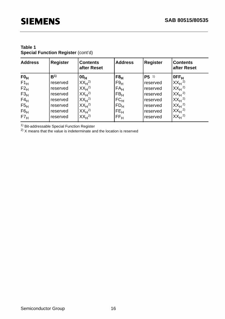
F0HF1HF2HF3HF4HF5HF6HF7H
B1)
reservedreservedreservedreservedreservedreservedreserved
00HXXH
2)
XXH2)
XXH2)
XXH2)
XXH2)
XXH2)
XXH2)
F8HF9HFAHFBHFCHFDHFEHFFH
P5 1)
reservedreservedreservedreservedreservedreservedreserved
0FFHXXH
2)
XXH2)
XXH2)
XXH2)
XXH2)
XXH2)
XXH2)
1) Bit-addressable Special Function Register2) X means that the value is indeterminate and the location is reserved
Table 1Special Function Register (cont’d)
Address Register Contentsafter Reset
Address Register Contentsafter Reset
SAB 80515/80535
Semiconductor Group 17
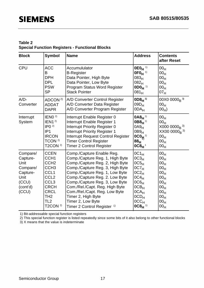
Table 2Special Function Registers - Functional Blocks
Block Symbol Name Address Contentsafter Reset
CPU ACCBDPHDPLPSWSP
AccumululatorB-RegisterData Pointer, High ByteData Pointer, Low ByteProgram Status Word RegisterStack Pointer
0E0H 1)
0F0H 1)
083H082H0D0H
1)
081H
00H00H00H00H00H07H
A/D-Converter
ADCON 2)
ADDATDAPR
A/D Converter Control RegisterA/D Converter Data RegisterA/D Converter Program Register
0D8H1)
09DH0DAH
00X0 0000B3)
00H00H)
InterruptSystem
IEN0 2)
IEN1 2)
IP0 2)
IP1IRCONTCON 2)
T2CON 2)
Interrupt Enable Register 0Interrupt Enable Register 1Interrupt Priority Register 0Interrupt Priority Register 1Interrupt Request Control RegisterTimer Control RegisterTimer 2 Control Register
0A8H 1)
0B8H 1)
0A9H0B9H0C0H
1)
88H1)
0C8H1
00H00HX000 0000B
3)
XX00 0000B3)
00H00H00H
Compare/Capture-UnitCompare/Capture-Unit(CCU)(cont’d)(CCU)
CCENCCH1CCH2CCH3CCL1CCL2CCL3CRCHCRCLTH2TL2T2CON 2)
Comp./Capture Enable Reg.Comp./Capture Reg. 1, High ByteComp./Capture Reg. 2, High ByteComp./Capture Reg. 3, High ByteComp./Capture Reg. 1, Low ByteComp./Capture Reg. 2. Low ByteComp./Capture Reg. 3, Low ByteCom./Rel./Capt. Reg. High ByteCom./Rel./Capt. Reg. Low ByteTimer 2, High ByteTimer 2, Low ByteTimer 2 Control Register 1)
0C1H0C3H0C5H0C7H0C2H0C4H0C6H0CBH0CAH0CDH0CCH0C8H
1)
00H00H00H00H00H00H00H00H00H00H00H00H
1) Bit-addressable special function registers2) This special function register is listed repeatedly since some bits of it also belong to other functional blocks3) X means that the value is indeterminate
SAB 80515/80535
Semiconductor Group 18
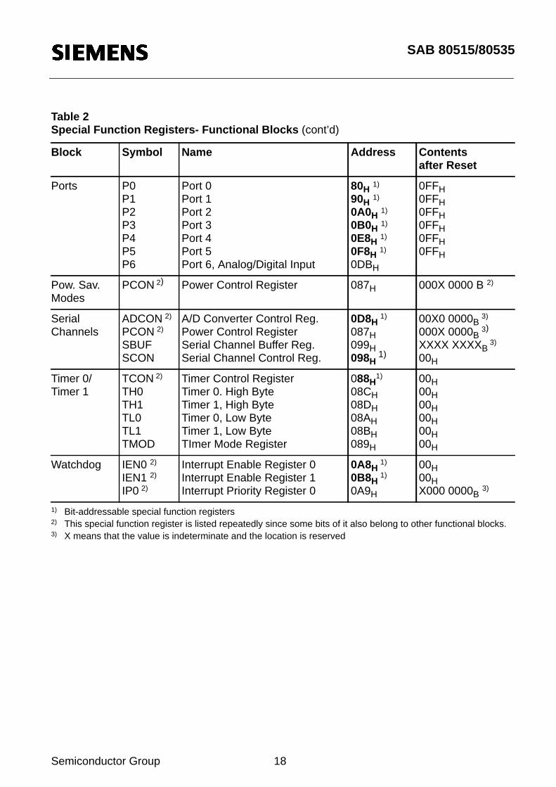
Table 2Special Function Registers- Functional Blocks (cont’d)
Block Symbol Name Address Contentsafter Reset
Ports P0P1P2P3P4P5P6
Port 0Port 1Port 2Port 3Port 4Port 5Port 6, Analog/Digital Input
80H1)
90H1)
0A0H1)
0B0H1)
0E8H1)
0F8H1)
0DBH
0FFH0FFH0FFH0FFH0FFH0FFH
Pow. Sav.Modes
PCON 2) Power Control Register 087H 000X 0000 B 2)
SerialChannels
ADCON 2)
PCON 2)
SBUFSCON
A/D Converter Control Reg.Power Control RegisterSerial Channel Buffer Reg.Serial Channel Control Reg.
0D8H1)
087H099H098H
1)
00X0 0000B3)
000X 0000B3)
XXXX XXXXB3)
00H
Timer 0/Timer 1
TCON 2)
TH0TH1TL0TL1TMOD
Timer Control RegisterTimer 0. High ByteTimer 1, High ByteTimer 0, Low ByteTimer 1, Low ByteTImer Mode Register
088H1)
08CH08DH08AH08BH089H
00H00H00H00H00H00H
Watchdog IEN0 2)
IEN1 2)
IP0 2)
Interrupt Enable Register 0Interrupt Enable Register 1Interrupt Priority Register 0
0A8H1)
0B8H1)
0A9H
00H00HX000 0000B
3)
1) Bit-addressable special function registers2) This special function register is listed repeatedly since some bits of it also belong to other functional blocks.3) X means that the value is indeterminate and the location is reserved
SAB 80515/80535
Semiconductor Group 19
Serial Port
The serial port of the SAB 80515 enables full duplex communication between microcontrollersor between microcontroller and peripheral devices. The serial port can operate in 4 modes:
Mode 0: Shift register mode. Serial data enters and exits through R×D. T×D outputs theshift clock. 8 bits are transmitted/received: 8 data bits (LSB first). The baud rateis fixed at 1/12 of the oscillator frequency.
Mode 1: 10 bits are transmitted (through R×D) or received (through T×D): a start bit (0),8 data bits (LSB first), and a stop bit (1). The baud rate is variable.
Mode 2: 11 bits are transmitted (through R×D) or received (through T×D): a start bit (0),8 data bits (LSB first), a programmable 9th data bit, and a stop bit (1). The baudrate is programmable to either 1/32 or 1/64 of the oscillator frequency.
Mode 3: 11 bits are transmitted (through T×D) or received (through R×D): a start bit (0),8 data bits (LSB first), a programmable 9th data bit, and a stop bit (1). Mode 3is identical to mode 2 except for the baud rate. The baud rate in mode 3 isvariable.
The variable baud rates in modes 1 and 3 can be generated by timer 1 or an internal baud rategenerator.
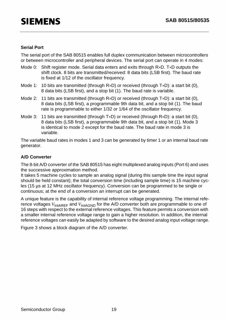
A/D Converter
The 8-bit A/D converter of the SAB 80515 has eight multiplexed analog inputs (Port 6) and usesthe successive approximation method.It takes 5 machine cycles to sample an analog signal (during this sample time the input signalshould be held constant); the total conversion time (including sample time) is 15 machine cyc-les (15 µs at 12 MHz oscillator frequency). Conversion can be programmed to be single orcontinuous; at the end of a conversion an interrupt can be generated.
A unique feature is the capability of internal reference voltage programming. The internal refe-rence voltages VIntAREF and VIntAGND for the A/D converter both are programmable to one of16 steps with respect to the external reference voltages. This feature permits a conversion witha smaller internal reference voltage range to gain a higher resolution. In addition, the internalreference voltages can easily be adapted by software to the desired analog input voltage range.
Figure 3 shows a block diagram of the A/D converter.
SAB 80515/80535
Semiconductor Group 20
Figure 3Block Diagram of the A/D Converter
SAB 80515/80535
Semiconductor Group 21
Timer/Counters
The SAB 80515 contains three 16-bit timer/counters which are useful in many applications fortiming and counting. The input clock for each timer/counter is 1/12 of the oscillator frequencyin the timer operation or can be taken from an external clock source for the counter operation(maximum count rate is 1/24 of the oscillator frequency).
– Timer/counter 0 and 1
These timer/counters can operate in four modes:
Mode 0: 8-bit timer/counter with 32:1 prescaler
Mode 1: 16-bit timer/counter
Mode 2: 8-bit timer/counter with 8-bit auto-reload
Mode 3: Timer/counter 0 is configured as one 8-bit timer/counter and one 8-bit timer;timer/counter 1 in this mode holds its count.
External inputs INT0 and INT1 can be programmed to function as a gate for timer/counters 0and 1 to facilitate pulse width measurements.
– Timer/counter 2
Timer/counter 2 of the SAB 80515 is a 16-bit timer/counter with several additional features. Itoffers a 2:1 prescaler, a selectable gate function, and compare, capture and reload functions.Corresponding to the 16-bit timer register there are four 16-bit capture/compare registers, oneof them can be used to perform a 16-bit reload on a timer overflow or external event. Each ofthese registers corresponds to a pin of port 1 for capture input/compare output.Figure 4 shows a block diagram of the timer/counter 2.
Reload
A 16-bit reload can be performed with the 16-bit CRC register, which is a concatenation of the8-bit registers CRCL and CRCH. There are two modes from which to select:
Mode 0: Reload is caused by a timer 2 overflow (auto-reload).
Mode 1: Reload is caused in response to a negative transition at pin T2EX (P1.5),which can also request an interrupt.
Capture
This feature permits saving the actual timer/counter contents into a selected register upon anexternal event or a software write operation. Two modes are provided to latch the current 16-bit value in timer 2 registers into a dedicated capture register:
Mode 0: Capture is performed in response to a transition at the corresponding port1 pins CC0 to CC3.
Mode 1: Write operation into the low-order byte of the dedicated capture registercauses the timer 2 contents to be latched into this register.
SAB 80515/80535
Semiconductor Group 22
Compare
In the compare mode, the 16-bit values stored in the dedicated compare registers are compa-red to the contents of the timer 2 registers. If the count value in the timer 2 registers matchesone of the stored values, an appropriate output signal is generated and an interrupt is requ-ested. Two compare modes are provided:
Mode 0: Upon a match the output signal changes from low to high. It goes back to a lowlevel when timer 2 overflows.
Mode 1: The transition of the output signal can be determined by software.A timer 2 overflow causes no output change.
SAB 80515/80535
Semiconductor Group 23
Figure 4Block Diagram of Timer/Counter 2
SAB 80515/80535
Semiconductor Group 24
Interrupt Structure
The SAB 80515 has 12 interrupt vectors with the following vector addresses and request flags:
Each interrupt vector can be individually enabled/disabled. The minimum response time to aninterrupt request is more than 3 machine cycles and less than 9 machine cycles.
Figure 5 shows the interrupt request sources.
External interrupts 0 and 1 can be activated by a low-level or a negative transition (selectable)at their corresponding input pin, external interrupts 2 and 3 can be programmed for triggeringon a negative or a positive transition. The external interrupts 3 to 6 are combined with the cor-responding alternate functions compare (output) and capture (input) on port 1.
For programming of the priority levels the interrupt vectors are combined to pairs. Each pair canbe programmed individually to one of four priority levels by setting or clearing one bit in thespecial function register IP0 and one in IP1. Figure 6 shows the priority level structure.
Table 3Interrupt Sources and Vectors
Source (Request Flags) Vector Address Vector
IE0TF0IE1TF1RI + TITF2 + EXF2IADCIEX2IEX3IEX4IEX5IEX6
0003H000BH0013H001BH0023H002BH0043H004BH0053H005BH0063H006BH
External interrupt 0Timer 0 interruptExternal interrupt 1Timer 1 interruptSerial port interruptTimer 2 interruptA/D converter interruptExternal interrupt 2External interrupt 3External interrupt 4External interrupt 5External interrupt 6
SAB 80515/80535
Semiconductor Group 25
Figure 5Interrupt Request Sources
SAB 80515/80535
Semiconductor Group 26
Figure 6Priority Level Structure
SAB 80515/80535
Semiconductor Group 27
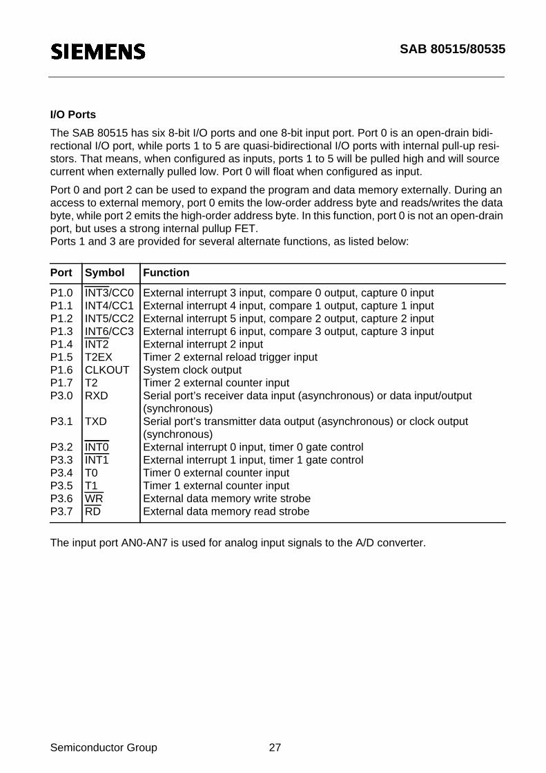
I/O Ports
The SAB 80515 has six 8-bit I/O ports and one 8-bit input port. Port 0 is an open-drain bidi-rectional I/O port, while ports 1 to 5 are quasi-bidirectional I/O ports with internal pull-up resi-stors. That means, when configured as inputs, ports 1 to 5 will be pulled high and will sourcecurrent when externally pulled low. Port 0 will float when configured as input.
Port 0 and port 2 can be used to expand the program and data memory externally. During anaccess to external memory, port 0 emits the low-order address byte and reads/writes the databyte, while port 2 emits the high-order address byte. In this function, port 0 is not an open-drainport, but uses a strong internal pullup FET.Ports 1 and 3 are provided for several alternate functions, as listed below:
The input port AN0-AN7 is used for analog input signals to the A/D converter.
Port Symbol Function
P1.0P1.1P1.2P1.3P1.4P1.5P1.6P1.7P3.0
P3.1
P3.2P3.3P3.4P3.5P3.6P3.7
INT3/CC0INT4/CC1INT5/CC2INT6/CC3INT2T2EXCLKOUTT2RXD
TXD
INT0INT1T0T1WRRD
External interrupt 3 input, compare 0 output, capture 0 inputExternal interrupt 4 input, compare 1 output, capture 1 inputExternal interrupt 5 input, compare 2 output, capture 2 inputExternal interrupt 6 input, compare 3 output, capture 3 inputExternal interrupt 2 inputTimer 2 external reload trigger inputSystem clock outputTimer 2 external counter inputSerial port’s receiver data input (asynchronous) or data input/output(synchronous)Serial port’s transmitter data output (asynchronous) or clock output(synchronous)External interrupt 0 input, timer 0 gate controlExternal interrupt 1 input, timer 1 gate controlTimer 0 external counter inputTimer 1 external counter inputExternal data memory write strobeExternal data memory read strobe
SAB 80515/80535
Semiconductor Group 28
Watchdog Timer
This feature is provided as a means of graceful recovery from a software upset. After an exter-nal reset, the watchdog timer is cleared and stopped. It can be started and cleared by software,but it cannot be stopped. If the software fails to clear the watchdog timer at least every 65532machine cycles (about 65 ms if a 12 MHz oscillator frequency is used), an internal hardwarereset will be initiated.
The reset cause (external reset or reset caused by the watchdog) can be examined by soft-ware. To clear the watchdog, two bits in two different special function registers must be set bytwo consecutive instructions (bits IEN0.6 and IEN1.6). This is done to prevent the watchdogfrom being cleared by unexpected opcodes.
Instruction Set Summary
The SAB 80515/80535 has the same instruction set as the industry standard 8051microcontroller.
A pocket guide is available which contains the complete instruction set in functional andhexadecimal order. Furtheron it provides helpful information about Special Function Registers,Interrupt Vectors and Assembler Directives.
Literature Information
Title Ordering No.
Microcontroller Family SAB 8051 Pocket Guide B158-B6599 - X - X - 7600
SAB 80515/80535
Semiconductor Group 29
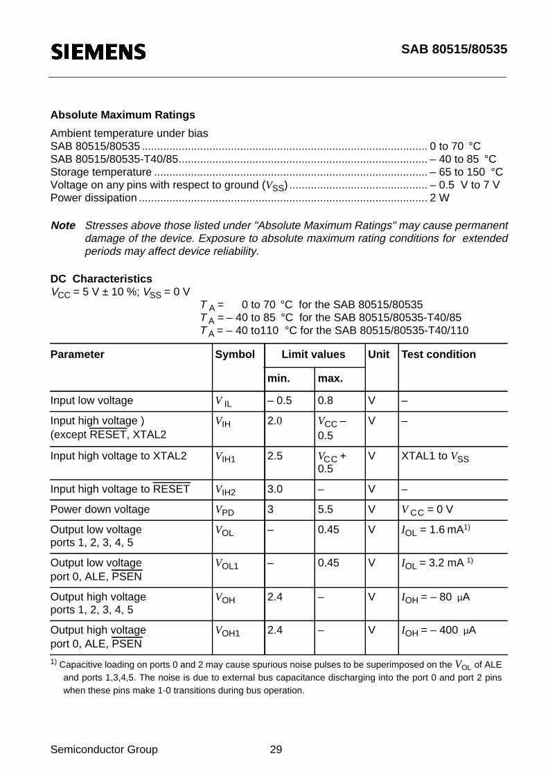
Absolute Maximum Ratings
Ambient temperature under biasSAB 80515/80535 ............................................................................................. 0 to 70 °CSAB 80515/80535-T40/85................................................................................. – 40 to 85 °CStorage temperature ......................................................................................... – 65 to 150 °CVoltage on any pins with respect to ground (VSS) ............................................. – 0.5 V to 7 VPower dissipation .............................................................................................. 2 W
Note Stresses above those listed under "Absolute Maximum Ratings" may cause permanentdamage of the device. Exposure to absolute maximum rating conditions for extendedperiods may affect device reliability.
DC CharacteristicsVCC = 5 V ± 10 %; VSS = 0 V
T A = 0 to 70 °C for the SAB 80515/80535T A = – 40 to 85 °C for the SAB 80515/80535-T40/85T A = – 40 to110 °C for the SAB 80515/80535-T40/110
Parameter Symbol Limit values Unit Test condition
min. max.
Input low voltage V IL – 0.5 0.8 V –
Input high voltage )(except RESET, XTAL2
VIH 2.0 VCC –0.5
V –
Input high voltage to XTAL2 VIH1 2.5 VCC +0.5
V XTAL1 to VSS
Input high voltage to RESET VIH2 3.0 – V –
Power down voltage VPD 3 5.5 V V CC = 0 V
Output low voltageports 1, 2, 3, 4, 5
VOL – 0.45 V IOL = 1.6 mA1)
Output low voltageport 0, ALE, PSEN
VOL1 – 0.45 V IOL = 3.2 mA 1)
Output high voltageports 1, 2, 3, 4, 5
VOH 2.4 – V IOH = – 80 µA
Output high voltageport 0, ALE, PSEN
VOH1 2.4 – V IOH = – 400 µA
1) Capacitive loading on ports 0 and 2 may cause spurious noise pulses to be superimposed on the VOL of ALEand ports 1,3,4,5. The noise is due to external bus capacitance discharging into the port 0 and port 2 pinswhen these pins make 1-0 transitions during bus operation.
SAB 80515/80535
Semiconductor Group 30
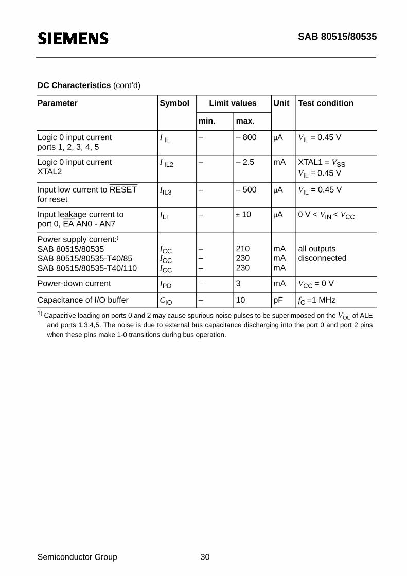
DC Characteristics (cont’d)
Parameter Symbol Limit values Unit Test condition
min. max.
Logic 0 input currentports 1, 2, 3, 4, 5
I IL – – 800 µA VIL = 0.45 V
Logic 0 input currentXTAL2
I IL2 – – 2.5 mA XTAL1 = VSSVIL = 0.45 V
Input low current to RESETfor reset
IIL3 – – 500 µA VIL = 0.45 V
Input leakage current toport 0, EA AN0 - AN7
ILI – ± 10 µA 0 V < VIN < VCC
Power supply current:)
SAB 80515/80535SAB 80515/80535-T40/85SAB 80515/80535-T40/110
ICCICCICC
–––
210230230
mAmAmA
all outputsdisconnected
Power-down current IPD – 3 mA VCC = 0 V
Capacitance of I/O buffer CIO – 10 pF fC =1 MHz
1) Capacitive loading on ports 0 and 2 may cause spurious noise pulses to be superimposed on the VOL of ALEand ports 1,3,4,5. The noise is due to external bus capacitance discharging into the port 0 and port 2 pinswhen these pins make 1-0 transitions during bus operation.
SAB 80515/80535
Semiconductor Group 31
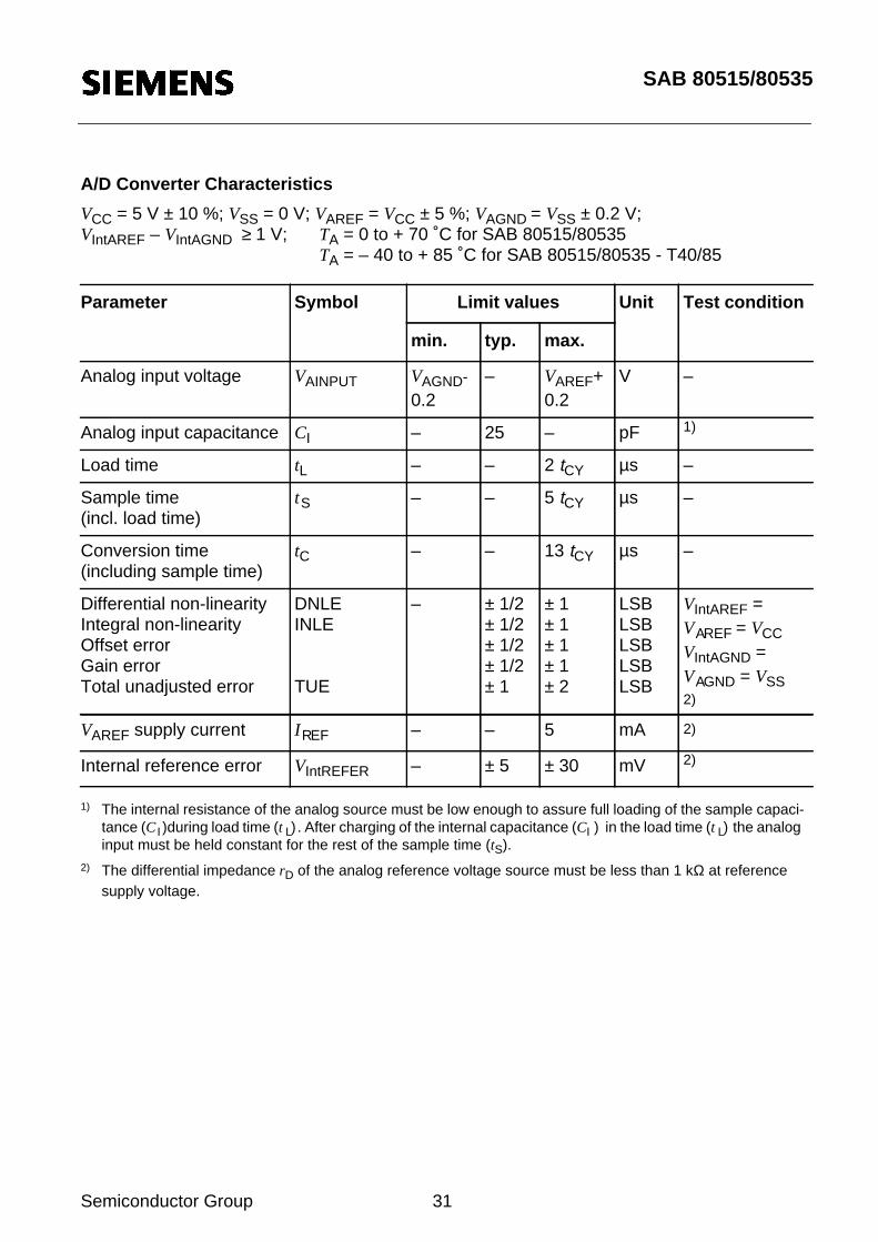
A/D Converter Characteristics
VCC = 5 V ± 10 %; VSS = 0 V; VAREF = VCC ± 5 %; VAGND = VSS ± 0.2 V;VIntAREF – VIntAGND ≥ 1 V; TA = 0 to + 70 ˚C for SAB 80515/80535
TA = – 40 to + 85 ˚C for SAB 80515/80535 - T40/85
Parameter Symbol Limit values Unit Test condition
min. typ. max.
Analog input voltage VAINPUT VAGND-
0.2– VAREF+
0.2V –
Analog input capacitance CI – 25 – pF 1)
Load time tL – – 2 tCY µs –
Sample time(incl. load time)
tS – – 5 tCY µs –
Conversion time(including sample time)
tC – – 13 tCY µs –
Differential non-linearityIntegral non-linearityOffset errorGain errorTotal unadjusted error
DNLEINLE
TUE
– ± 1/2± 1/2± 1/2± 1/2± 1
± 1± 1± 1± 1± 2
LSBLSBLSBLSBLSB
VIntAREF =VAREF = VCCVIntAGND =VAGND = VSS2)
VAREF supply current I REF – – 5 mA 2)
Internal reference error VIntREFER – ± 5 ± 30 mV 2)
1) The internal resistance of the analog source must be low enough to assure full loading of the sample capaci-tance (CI )during load time (t L ) . After charging of the internal capacitance (CI ) in the load time (t L ) the analoginput must be held constant for the rest of the sample time (tS).
2) The differential impedance rD of the analog reference voltage source must be less than 1 kΩ at referencesupply voltage.
SAB 80515/80535
Semiconductor Group 32
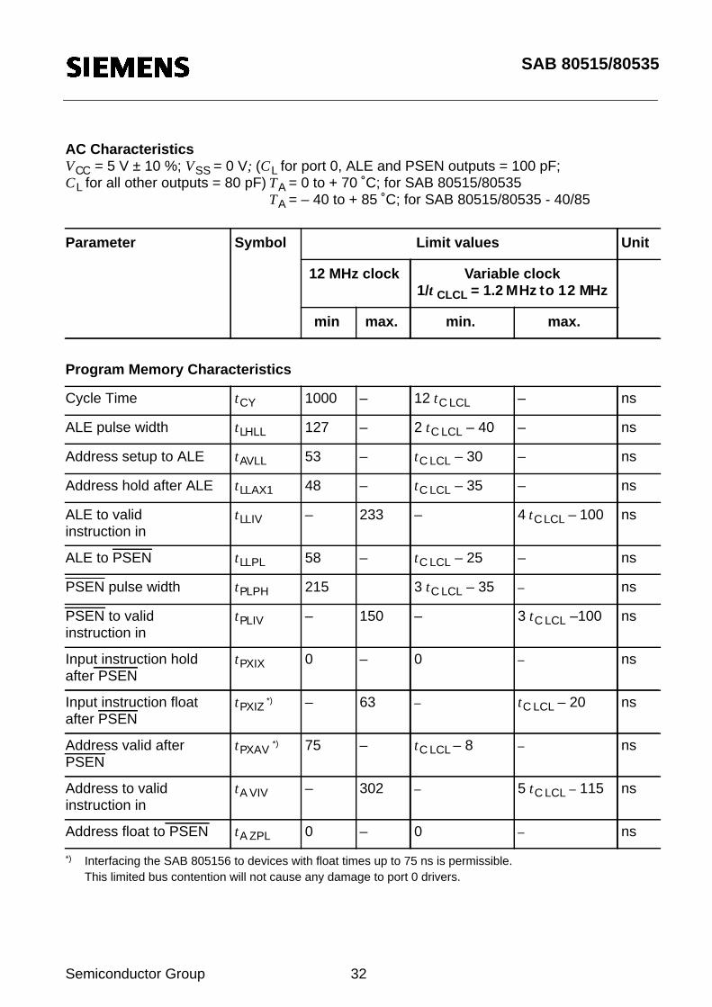
AC CharacteristicsVCC = 5 V ± 10 %; VSS = 0 V; (CL for port 0, ALE and PSEN outputs = 100 pF;CL for all other outputs = 80 pF) TA = 0 to + 70 ˚C; for SAB 80515/80535
TA = – 40 to + 85 ˚C; for SAB 80515/80535 - 40/85
Parameter Symbol Limit values Unit
12 MHz clock Variable clock1/t CLCL = 1.2 MHz to 12 MHz
min max. min. max.
Program Memory Characteristics
Cycle Time tCY 1000 – 12 tC LCL – ns
ALE pulse width tLHLL 127 – 2 tC LCL – 40 – ns
Address setup to ALE tAVLL 53 – tC LCL – 30 – ns
Address hold after ALE tLLAX1 48 – tC LCL – 35 – ns
ALE to validinstruction in
tLLIV – 233 – 4 tC LCL – 100 ns
ALE to PSEN tLLPL 58 – tC LCL – 25 – ns
PSEN pulse width tPLPH 215 3 tC LCL – 35 – ns
PSEN to validinstruction in
tPLIV – 150 – 3 tC LCL –100 ns
Input instruction holdafter PSEN
tPXIX 0 – 0 – ns
Input instruction floatafter PSEN
tPXIZ*) – 63 – tC LCL – 20 ns
Address valid afterPSEN
tPXAV*) 75 – tC LCL – 8 – ns
Address to validinstruction in
tA VIV – 302 – 5 tC LCL – 115 ns
Address float to PSEN tA ZPL 0 – 0 – ns
*) Interfacing the SAB 805156 to devices with float times up to 75 ns is permissible.This limited bus contention will not cause any damage to port 0 drivers.
SAB 80515/80535
Semiconductor Group 33
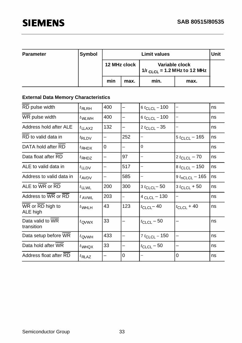
Parameter Symbol Limit values Unit
12 MHz clock Variable clock1/t CLCL = 1.2 MHz to 12 MHz
min max. min. max.
External Data Memory Characteristics
RD pulse width tRLRH 400 – 6 tCLCL – 100 – ns
WR pulse width tWLWH 400 – 6 tCLCL – 100 – ns
Address hold after ALE tLLAX2 132 – 2 tCLCL – 35 – ns
RD to valid data in tRLDV – 252 – 5 tCLCL – 165 ns
DATA hold after RD tRHDX 0 – 0 ns
Data float after RD tRHDZ – 97 – 2 tCLCL – 70 ns
ALE to valid data in tLLDV – 517 – 8 tCLCL – 150 ns
Address to valid data in tAVDV – 585 – 9 tnCLCL – 165 ns
ALE to WR or RD tLLWL 200 300 3 tCLCL– 50 3 tCLCL + 50 ns
Address to WR or RD t AVWL 203 – 4 CLCL – 130 – ns
WR or RD high toALE high
tWHLH 43 123 tCLCL– 40 tCLCL + 40 ns
Data valid to WRtransition
tQVWX 33 – tCLCL – 50 – ns
Data setup before WR tQVWH 433 – 7 tCLCL – 150 – ns
Data hold after WR tWHQX 33 – tCLCL – 50 – ns
Address float after RD tRLAZ – 0 – 0 ns
SAB 80515/80535
Semiconductor Group 34
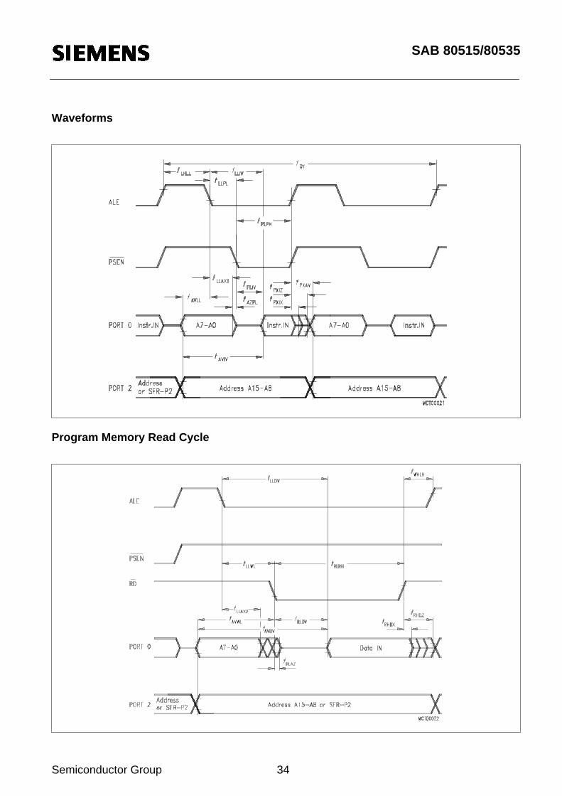
Waveforms
Program Memory Read Cycle
SAB 80515/80535
Semiconductor Group 35
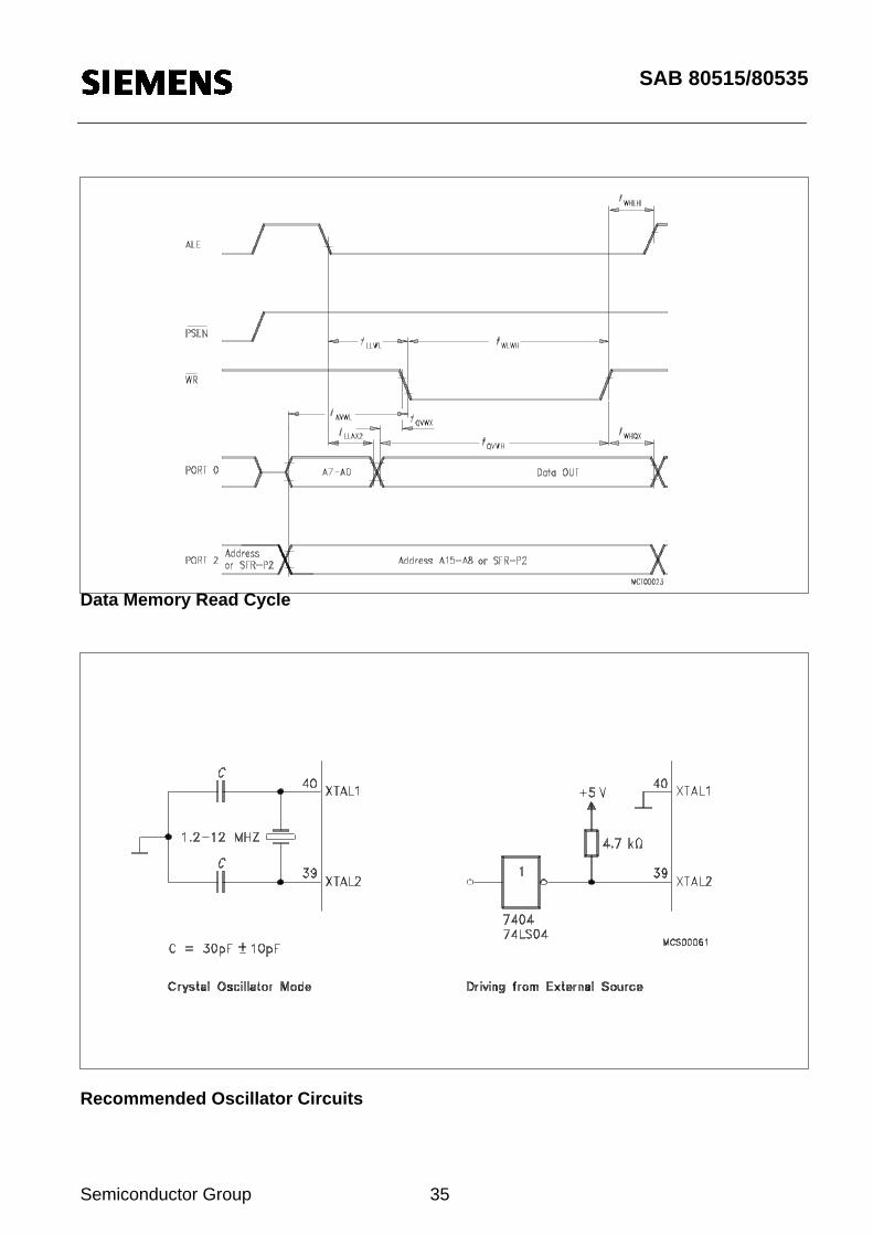
Data Memory Read Cycle
Recommended Oscillator Circuits
SAB 80515/80535
Semiconductor Group 36
AC Characteristics (cont’d)
External Clock Cycle
Parameter Symbol Limit values Unit
Variable clockFrequ. = 1.2 MHz to 12 MHz
min. max.
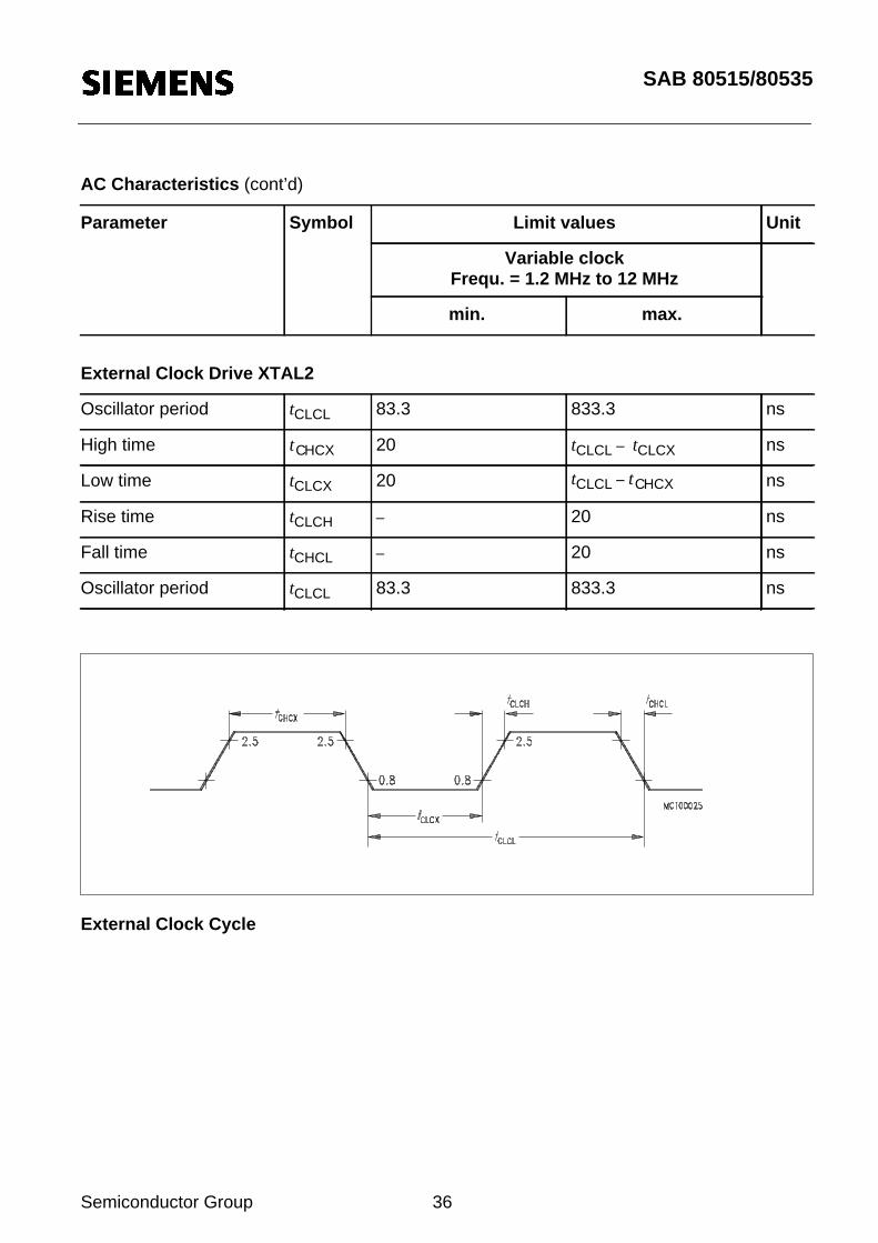
External Clock Drive XTAL2
Oscillator period tCLCL 83.3 833.3 ns
High time tCHCX 20 tCLCL – tCLCX ns
Low time tCLCX 20 tCLCL – tCHCX ns
Rise time tCLCH – 20 ns
Fall time tCHCL – 20 ns
Oscillator period tCLCL 83.3 833.3 ns
SAB 80515/80535
Semiconductor Group 37
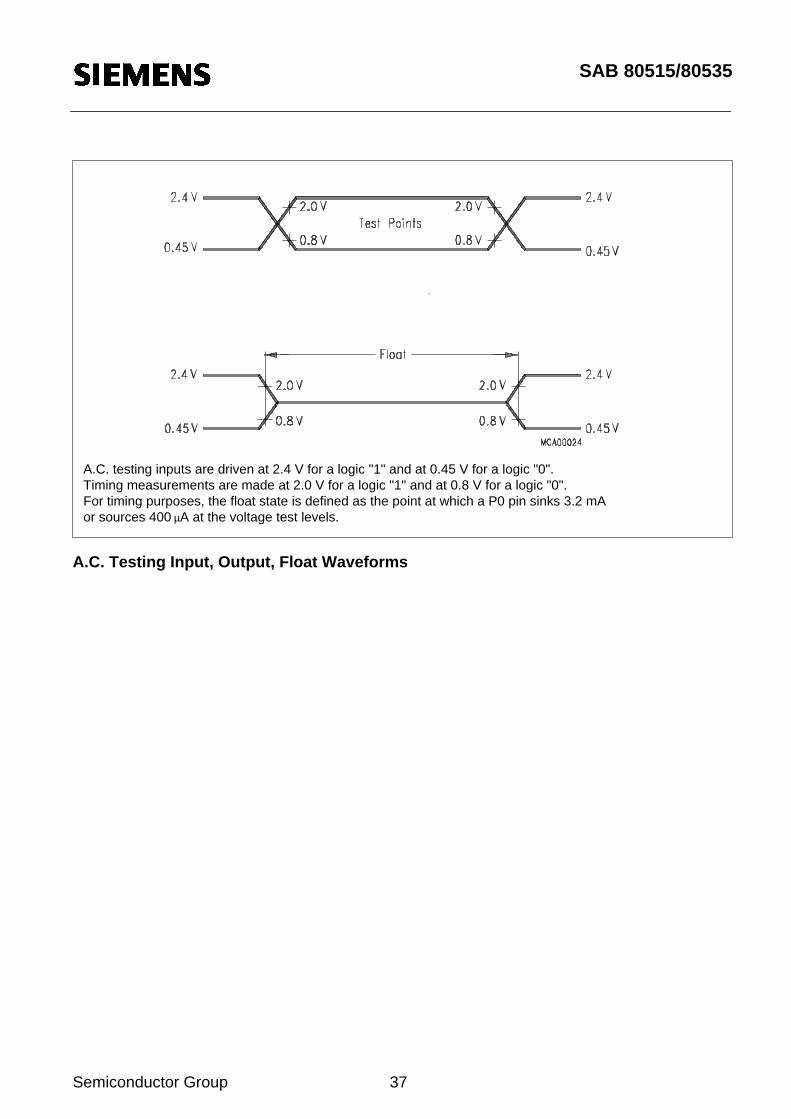
A.C. Testing Input, Output, Float Waveforms
A.C. testing inputs are driven at 2.4 V for a logic "1" and at 0.45 V for a logic "0".Timing measurements are made at 2.0 V for a logic "1" and at 0.8 V for a logic "0".For timing purposes, the float state is defined as the point at which a P0 pin sinks 3.2 mAor sources 400 µA at the voltage test levels.
SAB 80515/80535
Semiconductor Group 38
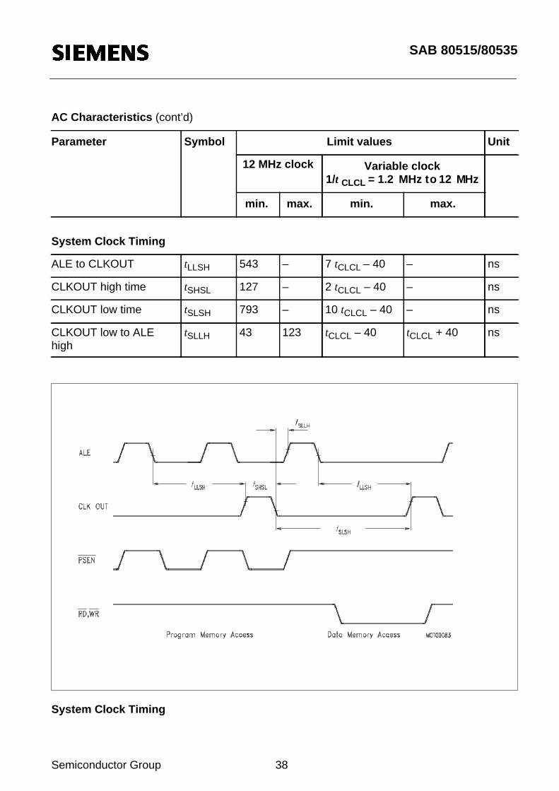
System Clock Timing
AC Characteristics (cont’d)
Parameter Symbol Limit values Unit
12 MHz clock Variable clock1/t CLCL = 1.2 MHz to 12 MHz
min. max. min. max.
System Clock Timing
ALE to CLKOUT tLLSH 543 – 7 tCLCL – 40 – ns
CLKOUT high time tSHSL 127 – 2 tCLCL – 40 – ns
CLKOUT low time tSLSH 793 – 10 tCLCL – 40 – ns
CLKOUT low to ALEhigh
tSLLH 43 123 tCLCL – 40 tCLCL + 40 ns
SAB 80515/80535
Semiconductor Group 39
ROM Verification Characteristics
TA = 25 ˚C ± 5 ˚C; VCC = 5 V ± 10 %; VSS = 0 V
ROM Verification
Parameter Symbol Limit values Unit
min max.
ROM Verification
Address to valid data tAVQV – 48 tCLCL1 ns
ENABLE to valid data tELQV – 48 tCLCL1 ns
Data float after ENABLE tEHOZ 0 48 tCLCL1 ns
Oscillator frequency 1/tCLCL 4 6 MHz
Address: P1.0-P1.7 = A0-A7P2.0-P2.4 = A8-A12
Data: Port 0 = D0-D7
Inputs: P2.5-P2.6, PSEN = VSSALE, EA = VIHRESET = VIL
SAB 80515/80535
Semiconductor Group 40
Package Outlines
Plastic Package, P-LCC-68 – SMD(Plastic Leaded Chip-Carrier)
Sorts of PackingPackage outlines for tubes, trays etc. are contained in ourData Book “Package Information”.
Dimensions in mmSMD = Surface Mounted Device