Embed Size (px)
Citation preview

8/20/2019 Microcontroller Voltmeter
http://slidepdf.com/reader/full/microcontroller-voltmeter 1/28
1
INTRODUCTION
A voltmeter finds its importance wherever voltage is to be measured.
A voltmeter is an instrument used for measuring the electrical potential difference
between two points in an electric circuit. Analog voltmeters move a pointer across a
scale in proportion to the voltage of the circuit. General purpose analog voltmeters may
have an accuracy of a few per cent of full scale, and are used with voltages from a
fraction of a volt to several thousand volts.
Digital voltmeters give a numerical display of voltage by use of analog to digital
converter. Digital meters can be made with high accuracy, typically better than 1%.
Specially calibrated test instruments have higher accuracies, with laboratory instruments capable of measuring to accuracies of a few parts per million. Meters
using amplifiers can measure tiny voltages of micro‐volts or less. Digital voltmeters
(DVMs) are usually designed around a special type of analog‐to‐digital converter called
an integrating converter. Voltmeter accuracy is affected by many factors, including
temperature and supply voltage variations. To ensure that a digital voltmeter's reading is
within the manufacturer's specified tolerances, they should be periodically calibrated.
Digital voltmeters necessarily have input amplifiers, and, like vacuum tube voltmeters,
generally have a constant input resistance of 10 mega‐ohms regardless of set
measurement range.
This project aims at building a Digital Voltmeter using an 8051 microcontroller. All the
data accessed and processed by the microcontroller is the digital data. And thus, the
usage of an analog‐to‐digital converter finds its necessity here. A standard analog‐to‐
digital converter ADC0804 is used in the current project. The input voltage (which is the
analog input) is restricted to be in the range of 0‐15V. The processed data in the 8051 is
used to drive a display output on a LCD display unit. The display is in the form of digits
and is accurate to a value of one decimal. The input voltage is desired to be that of a DC
voltage for steady observations of the voltage value on the LCD panel. Rather, if an AC
input voltage is given at the input terminals, the output varies indefinitely as is the
nature of AC voltage. Thus, the instantaneous value of the AC voltage is not steadily
shown on the LCD panel.

8/20/2019 Microcontroller Voltmeter
http://slidepdf.com/reader/full/microcontroller-voltmeter 2/28
2
COMPONENTS
Following is the entire set of the components used to build the Digital Voltmeter:
1. Microcontroller, AT89S52
2. Analog‐to‐Digital Converter, ADC0804
3. 16x1 LCD
4. Oscillator circuit for the microcontroller
4.1 12MHz Crystal Capacitor
4.2
33pF Capacitors
5. Voltage divider circuit/ Input terminals
5.1 200k, 100k Resistors
5.2 100nF Capacitor
6. ADC Clock Circuit
6.1 10k Resistor
6.2
150pF Capacitor
7. 100k Potentiometer (to adjust the back‐light of the LCD)
8/20/2019 Microcontroller Voltmeter
http://slidepdf.com/reader/full/microcontroller-voltmeter 3/28
3
Description of the Components used
Microcontroller, AT89S52
The AT89S51 is a low‐power, high‐performance CMOS 8‐bit microcontroller with 4K
bytes of In‐System Programmable Flash memory. The device is manufactured using
Atmel’s high‐density non‐volatile memory technology and is compatible with the
industry‐standard 80C51 instruction set and pin‐out. The on‐chip Flash allows the
program memory to be reprogrammed in‐system or by a conventional non‐volatile
memory programmer. By combining a versatile 8‐bit CPU with In‐System Programmable
Flash on a monolithic chip, the Atmel AT89S51 is a powerful microcontroller which
provides a highly‐flexible and cost‐effective solution to many embedded control
applications. The AT89S51 provides the following standard features: 4K bytes of Flash,
128 bytes of RAM, 32 I/O lines, Watchdog timer, two data pointers, two 16‐bit
timer/counters, a five‐vector two‐level interrupt architecture, a full duplex serial port,
on‐chip oscillator, and clock circuitry.
In addition, the AT89S51 is designed with static logic for operation down to zero
frequency and supports two software selectable power saving modes. The Idle mode
stops the CPU while allowing the RAM, timer/counters, serial port, and interrupt system
to continue functioning. The Power‐down mode saves the RAM con‐tents but freezes
the oscillator, disabling all other chip functions until the next external interrupt or
hardware reset.
Pin configuration of the AT89S52 is as follows:
40‐Lead PDIP
8/20/2019 Microcontroller Voltmeter
http://slidepdf.com/reader/full/microcontroller-voltmeter 4/28
4
VCC
Supply voltage.
GND Ground.
Port 0 Port 0 is an 8‐bit open drain bi‐directional I/O port. As an output port, each pin
can sink eight TTL inputs. When 1s are written to port 0 pins, the pins can be used as
high‐impedance inputs. Port 0 can also be configured to be the multiplexed low‐order
address/data bus during accesses to external program and data memory. In this mode,
P0 has internal pull‐ups. Port 0 also receives the code bytes during Flash programming
and
outputs
the
code
bytes
during
program
verification.
External
pull‐
ups
are
required
during program verification.
Port 1 Port 1 is an 8‐bit bi‐directional I/O port with internal pull‐ups. The Port 1 output
buffers can sink/source four TTL inputs. When 1s are written to Port 1 pins, they are
pulled high by the internal pull‐ups and can be used as inputs. As inputs, Port 1 pins that
are externally being pulled low will source current (IIL) because of the internal pull‐ups.
Port 1 also receives the low‐order address bytes during Flash programming and
verification.
8/20/2019 Microcontroller Voltmeter
http://slidepdf.com/reader/full/microcontroller-voltmeter 5/28
5
P1.5 MOSI (used for In‐System Programming)
P1.6 MISO (used for In‐System Programming)
P1.7 SCK (used for In‐System Programming)
Port 2 Port 2 is an 8‐bit bi‐directional I/O port with internal pull‐ups. The Port 2 output
buffers can sink/source four TTL inputs. When 1s are written to Port 2 pins, they are
pulled high by the internal pull‐ups and can be used as inputs. As inputs, Port 2 pins that
are externally being pulled low will source current (IIL) because of the internal pull‐ups.
Port 2 emits the high‐order address byte during fetches from external program memory
and during accesses to external data memory that use 16‐bit addresses (MOVX @ DPTR).
In this application, Port 2 uses strong internal pull‐ups when emitting 1s. During accesses to external data memory that use 8‐bit addresses (MOVX @ RI), Port 2 emits the
contents of the P2 Special Function Register. Port 2 also receives the high‐order address
bits and some control signals during Flash programming and verification.
Port 3 Port 3 is an 8‐bit bi‐directional I/O port with internal pull‐ups. The Port 3 output
buffers can sink/source four TTL inputs. When 1s are written to Port 3 pins, they are
pulled high by the internal pull‐ups and can be used as inputs. As inputs, Port 3 pins that
are externally being pulled low will source current (IIL) because of the pull‐ups. Port 3
receives some control signals for Flash programming and verification. Port 3 also serves
the functions of various special features of the AT89S51, as shown in the following table.
Alternate functions of port 3,
P3.0 RXD (serial input port)
P3.1 TXD (serial output port)
P3.2 INT0 (external interrupt 0)
P3.3 INT1 (external interrupt 1)
P3.4 T0 (timer 0 external input)
P3.5 T1 (timer 1 external input)
P3.6 WR (external data memory write strobe)
P3.7 RD
(external
data
memory
read
strobe)
8/20/2019 Microcontroller Voltmeter
http://slidepdf.com/reader/full/microcontroller-voltmeter 6/28
6
RST Reset input. A high on this pin for two machine cycles while the oscillator is
running resets the device. This pin drives High for 98 oscillator periods after the
Watchdog
times
out.
The
DIS‐
RTO
bit
in
SFR
AUXR
(address
8EH)
can
be
used
to
disable
this feature. In the default state of bit DISRTO, the RESET HIGH out feature is enabled.
ALE/PROG Address Latch Enable (ALE) is an output pulse for latching the low byte of
the address during accesses to external memory. This pin is also the program pulse input
(PROG) during Flash programming. In normal operation, ALE is emitted at a constant
rate of 1/6 the oscillator frequency and may be used for external timing or clocking
purposes. Note, however, that one ALE pulse is skipped during each access to external
data memory. If desired, ALE operation can be disabled by setting bit 0 of SFR location
8EH. With the bit set, ALE is active only during a MOVX or MOVC instruction. Otherwise,
the pin is weakly pulled high. Setting the ALE‐disable bit has no effect if the
microcontroller is in external execution mode.
PSEN Program Store Enable (PSEN) is the read strobe to external program memory.
When the AT89S51 is executing code from external program memory, PSEN is activated
twice each machine cycle, except that two PSEN activations are skipped during each access to external data memory.
EA/VPP External Access Enable. EA must be strapped to GND in order to enable the
device to fetch code from external program memory locations starting at 0000H up to
FFFFH. Note, however, that if lock bit 1 is programmed, EA will be internally latched on
reset. EA should be strapped to VCC for internal program executions. This pin also
receives
the
12‐
volt
programming
enable
voltage
(VPP)
during
Flash
programming.
XTAL1 Input to the inverting oscillator amplifier and input to the internal clock
operating circuit.
XTAL2 Output from the inverting oscillator amplifier.
8/20/2019 Microcontroller Voltmeter
http://slidepdf.com/reader/full/microcontroller-voltmeter 7/28
7
Memory Organisation,
Program Memory: ‐ If the EA pin is connected to GND, all program fetches are directed
to external memory. On the AT89S51, if EA is connected to VCC, program fetches to
addresses
0000H
through
FFFH
are
directed
to
internal
memory
and
fetches
to
addresses 1000H through FFFFH are directed to external memory.
Data Memory: ‐ The AT89S51 implements 128 bytes of on‐chip RAM. The 128 bytes are
accessible via direct and indirect addressing modes. Stack operations are examples of
indirect addressing, so the 128 bytes of data RAM are available as stack space.
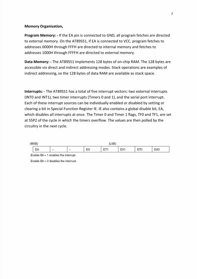
Interrupts: ‐ The AT89S51 has a total of five interrupt vectors: two external interrupts
(INT0 and INT1), two timer interrupts (Timers 0 and 1), and the serial port interrupt. Each of these interrupt sources can be individually enabled or disabled by setting or
clearing a bit in Special Function Register IE. IE also contains a global disable bit, EA,
which disables all interrupts at once. The Timer 0 and Timer 1 flags, TF0 and TF1, are set
at S5P2 of the cycle in which the timers overflow. The values are then polled by the
circuitry in the next cycle.
8/20/2019 Microcontroller Voltmeter
http://slidepdf.com/reader/full/microcontroller-voltmeter 8/28
8
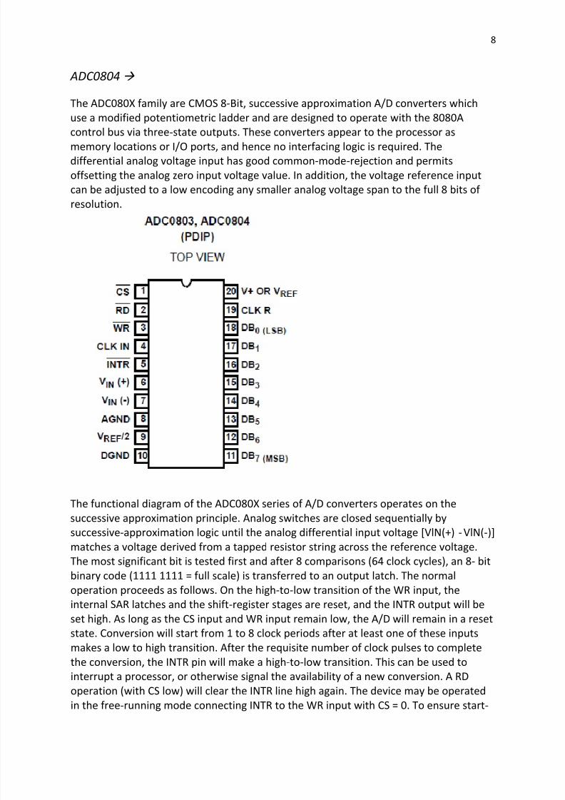
ADC0804
The ADC080X family are CMOS 8‐Bit, successive approximation A/D converters which
use a modified potentiometric ladder and are designed to operate with the 8080A
control bus via three‐state outputs. These converters appear to the processor as
memory locations or I/O ports, and hence no interfacing logic is required. The
differential analog voltage input has good common‐mode‐rejection and permits
offsetting the analog zero input voltage value. In addition, the voltage reference input
can be adjusted to a low encoding any smaller analog voltage span to the full 8 bits of
resolution.
The functional diagram of the ADC080X series of A/D converters operates on the
successive approximation principle. Analog switches are closed sequentially by
successive‐approximation logic until the analog differential input voltage [VlN(+) ‐VlN(‐)]
matches a voltage derived from a tapped resistor string across the reference voltage.
The most significant bit is tested first and after 8 comparisons (64 clock cycles), an 8‐ bit binary code (1111 1111 = full scale) is transferred to an output latch. The normal
operation proceeds as follows. On the high‐to‐low transition of the WR input, the
internal SAR latches and the shift‐register stages are reset, and the INTR output will be
set high. As long as the CS input and WR input remain low, the A/D will remain in a reset
state. Conversion will start from 1 to 8 clock periods after at least one of these inputs
makes a low to high transition. After the requisite number of clock pulses to complete
the conversion, the INTR pin will make a high‐to‐low transition. This can be used to
interrupt a processor, or otherwise signal the availability of a new conversion. A RD
operation (with CS low) will clear the INTR line high again. The device may be operated
in the free‐running mode connecting INTR to the WR input with CS = 0. To ensure start‐
8/20/2019 Microcontroller Voltmeter
http://slidepdf.com/reader/full/microcontroller-voltmeter 9/28
9
up under all possible conditions, an external WR pulse is required during the first power‐
up cycle. A conversion in process can be interrupted by issuing a second start command.
Digital Operation
The converter is started by having CS and WR simultaneously low. This sets the start flip‐
flop (F/F) and the resulting “1” level resets the 8‐bit shift register, resets the Interrupt
(INTR) F/F and inputs a “1” to the D flip‐flop, DFF1, which is at the input end of the 8‐bit
shift register. Internal clock signals then transfer this “1” to the Q output of DFF1. The
AND gate, G1, combines this “1” output with a clock signal to provide a reset signal to
the start F/F. If the set signal is no longer present (either WR or CS is a “1”), the start F/F
is reset and the 8‐bit shift register then can have the “1” clocked in, which starts the
conversion process. If the set signal were to still be present, this reset pulse would have
no effect (both outputs of the start F/F would be at a “1” level) and the 8‐bit shift
register would continue to be held in the reset mode. This allows for asynchronous or
wide CS and WR signals. After the “1” is clocked through the 8‐bit shift register (which completes the SAR operation) it appears as the input to DFF2. As soon as this “1” is
output from the shift register, the AND gate, G2, causes the new digital word to transfer
to the Three‐State output latches. When DFF2 is subsequently clocked, the Q output
makes a high‐to‐low transition which causes the INTR F/F to set. An inverting buffer then
supplies the INTR output signal. When data is to be read, the combination of both CS
and RD being low will cause the INTR F/F to be reset and the three state output latches
will be enabled to provide the 8‐bit digital outputs.
Digital Control
Inputs
The digital control inputs (CS, RD, and WR) meet standard TTL logic voltage levels. These
signals are essentially equivalent to the standard A/D Start and Output Enable control
signals, and are active low to allow an easy interface to microprocessor control busses.
For non‐microprocessor based applications, the CS input (pin 1) can be grounded and
the standard A/D Start function obtained by an active low pulse at the WR input (pin 3).
The Output Enable function is achieved by an active low pulse at the RD input (pin 2).
Analog Operation
The analog comparisons are performed by a capacitive charge summing circuit. Three
capacitors (with precise ratioed values) share a common node with the input to an
autozeroed comparator. The input capacitor is switched between VlN(+) and VlN(‐),
while two ratioed reference capacitors are switched between taps on the reference
voltage divider string. The net charge corresponds to the weighted difference between
the input and the current total value set by the successive approximation register. A
correction is made to offset the comparison by 1/2 LSB.
8/20/2019 Microcontroller Voltmeter
http://slidepdf.com/reader/full/microcontroller-voltmeter 10/28
10
Analog Differential Voltage Inputs and Common‐
Mode Rejection
This A/D gains considerable applications flexibility from the analog differential voltage
input. The VlN(‐) input (pin 7) can be used to automatically subtract a fixed voltage value
from the input reading (tare correction). This is also useful in 4mA ‐20mA current loop
conversion. In addition, common‐mode noise can be reduced by use of the differential
input. The time interval between sampling VIN(+) and VlN(‐) is 41/2 clock periods. There
is maximum error voltage due to this slight time difference between the input voltage
samples.
The allowed range of analog input voltage usually places more severe restrictions on
input common‐mode voltage levels than this. An analog input voltage with a reduced
span and a relatively large zero offset can be easily handled by making use of the
differential input.
Analog Input Current
The internal switching action causes displacement currents to flow at the analog inputs.
The voltage on the on‐chip capacitance to ground is switched through the analog
differential input voltage, resulting in proportional currents entering the VIN(+) input
and leaving the VIN(‐) input. These current transients occur at the leading edge of the
internal clocks. They rapidly decay and do not inherently cause errors as the on‐chip
comparator is strobed at the end of the clock period.
Input Bypass Capacitors
Bypass capacitors at the inputs will average these charges and cause a DC current to flow through the output resistances of the analog signal sources. This charge pumping
action is worse for continuous conversions with the VIN(+) input voltage at full scale. For
a 640kHz clock frequency with the VIN(+) input at 5V, this DC current is at a maximum of
approximately 5uA. Therefore, bypass capacitors should not be used at the analog
inputs or the VREF/2 pin for high resistance sources (>1kOhm.) If input bypass capacitors
are necessary for noise filtering and high source resistance is desirable to minimize
capacitor size, the effects of the voltage drop across this input resistance, due to the
average value of the input current, can be compensated by a full scale adjustment while
the given source resistor and input bypass capacitor are both in place. This is possible
because the average value of the input current is a precise linear function of the
differential input voltage at a constant conversion rate.
Input Source Resistance
Large values of source resistance where an input bypass capacitor is not used will not
cause errors since the input currents settle out prior to the comparison time. If a low‐
pass filter is required in the system, use a low‐value series resistor for a passive RC
section or add an op amp RC active low‐pass filter. For low‐source‐resistance
applications, a 0.1uF bypass capacitor at the inputs will minimize EMI due to the series
lead inductance of a long wire. A 100Ohm series resistor can be used to isolate this
8/20/2019 Microcontroller Voltmeter
http://slidepdf.com/reader/full/microcontroller-voltmeter 11/28
11
capacitor (both the R and C are placed outside the feedback loop) from the output of an
op amp, if used.
Stray Pickup
The leads to the analog inputs (pins 6 and 7) should be kept as short as possible to
minimize stray signal pickup (EMI). Both EMI and undesired digital‐clock coupling to
these inputs can cause system errors. The source resistance for these inputs should, in
general, be kept below 5kΩ. Larger values of source resistance can cause undesired
signal pickup. Input bypass capacitors, placed from the analog inputs to ground, will
eliminate this pickup but can create analog scale errors as these capacitors will average
the transient input switching currents of the A/D (see Analog Input Current). This scale
error depends on both a large source resistance and the use of an input bypass
capacitor. This error can be compensated by a full scale adjustment of the A/D (see Full
Scale Adjustment) with the source resistance and input bypass capacitor in place, and
the desired conversion rate.
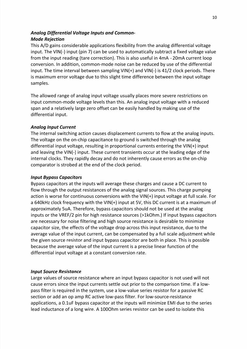
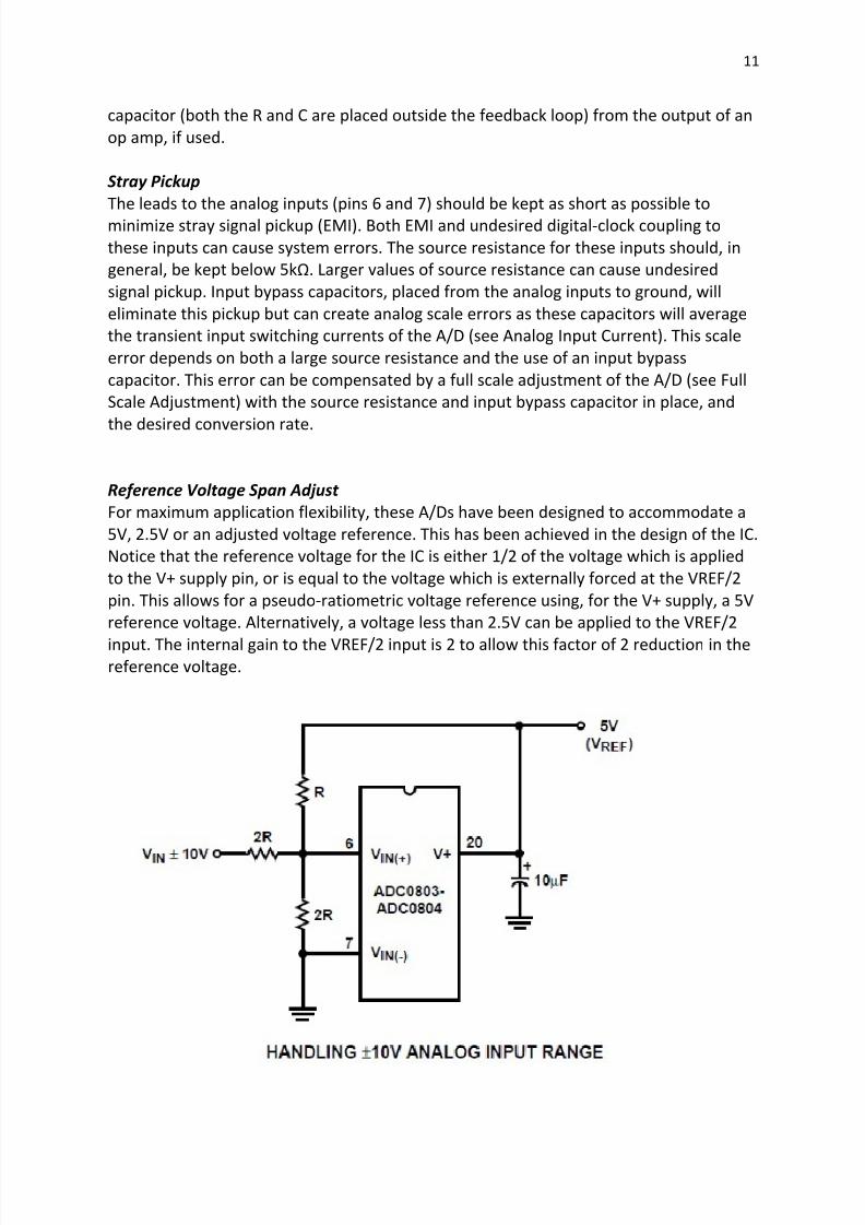
Reference Voltage Span Adjust
For maximum application flexibility, these A/Ds have been designed to accommodate a
5V, 2.5V or an adjusted voltage reference. This has been achieved in the design of the IC.
Notice that the reference voltage for the IC is either 1/2 of the voltage which is applied
to the V+ supply pin, or is equal to the voltage which is externally forced at the VREF/2
pin. This allows for a pseudo‐ratiometric voltage reference using, for the V+ supply, a 5V
reference voltage. Alternatively, a voltage less than 2.5V can be applied to the VREF/2
input. The internal gain to the VREF/2 input is 2 to allow this factor of 2 reduction in the reference voltage.
8/20/2019 Microcontroller Voltmeter
http://slidepdf.com/reader/full/microcontroller-voltmeter 12/28
12
Zero Error
The zero of the A/D does not require adjustment. If the minimum analog input voltage
value, VlN(MlN), is not ground, a zero offset can be done. The converter can be made to
output 0000 0000 digital code for this minimum input voltage by biasing the A/D VIN(‐)
input at this VlN(MlN) value. This utilizes the differential mode operation of the A/D. The
zero error of the A/D converter relates to the location of the first riser of the transfer
function and can be measured by grounding the VIN(‐) input and applying a small magnitude positive voltage to the VIN(+) input. Zero error is the difference between the
actual DC input voltage which is necessary to just cause an output digital code transition
from 0000 0000 to 0000 0001 and the ideal 1/2 LSB value (1/2 LSB = 9.8mV for VREF/2 =
2.500V).
Full Scale Adjust
The full scale adjustment can be made by applying a differential input voltage which is
11/2 LSB down from the desired analog full scale voltage range and then adjusting the
magnitude of the VREF/2 input (pin 9) for a digital output code which is just changing from 1111 1110 to 1111 1111. When offsetting the zero and using a span‐adjusted
VREF/2 voltage, the full scale adjustment is made by inputting VMlN to the VIN(‐) input
of the A/D and applying a voltage to the VIN(+) input.
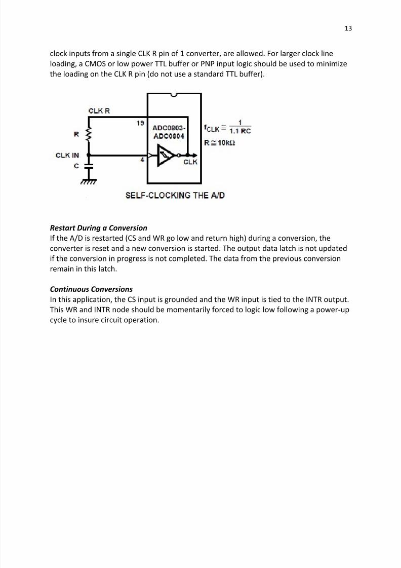
Clocking Option
The clock for the A/D can be derived from an external source such as the CPU clock or an
external RC network can be added to provide self ‐clocking. The CLK IN (pin 4) makes use
of a Schmitt trigger.
Heavy capacitive or DC loading of the CLK R pin should be avoided as this will disturb
normal converter operation. Loads less than 50pF, such as driving up to 7 A/D converter
8/20/2019 Microcontroller Voltmeter
http://slidepdf.com/reader/full/microcontroller-voltmeter 13/28
13
clock inputs from a single CLK R pin of 1 converter, are allowed. For larger clock line
loading, a CMOS or low power TTL buffer or PNP input logic should be used to minimize
the loading on the CLK R pin (do not use a standard TTL buffer).
Restart During a Conversion
If the A/D is restarted (CS and WR go low and return high) during a conversion, the
converter is reset and a new conversion is started. The output data latch is not updated
if the conversion in progress is not completed. The data from the previous conversion
remain in this latch.
Continuous Conversions
In this application, the CS input is grounded and the WR input is tied to the INTR output. This WR and INTR node should be momentarily forced to logic low following a power‐up
cycle to insure circuit operation.
8/20/2019 Microcontroller Voltmeter
http://slidepdf.com/reader/full/microcontroller-voltmeter 14/28
14
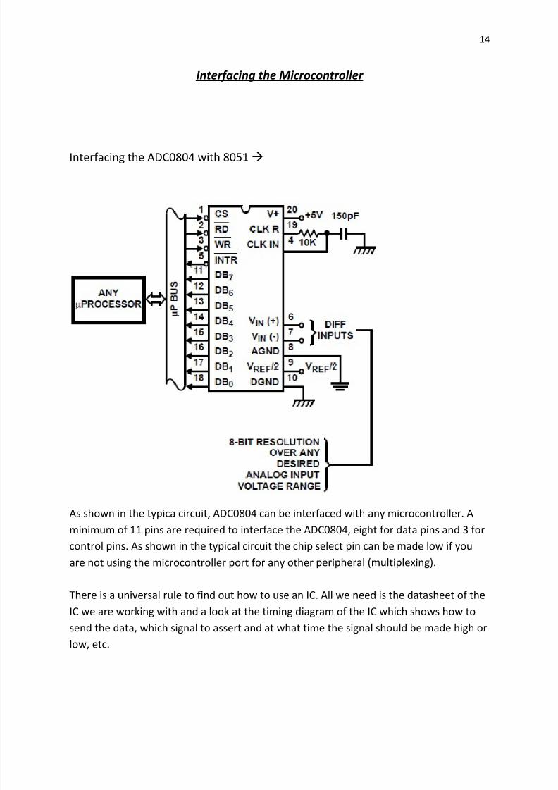
Interfacing the Microcontroller
Interfacing the ADC0804 with 8051
As shown in the typica circuit, ADC0804 can be interfaced with any microcontroller. A
minimum of 11 pins are required to interface the ADC0804, eight for data pins and 3 for
control pins. As shown in the typical circuit the chip select pin can be made low if you
are not using the microcontroller port for any other peripheral (multiplexing).
There is a universal rule to find out how to use an IC. All we need is the datasheet of the
IC we are working with and a look at the timing diagram of the IC which shows how to
send the data, which signal to assert and at what time the signal should be made high or
low, etc.
8/20/2019 Microcontroller Voltmeter
http://slidepdf.com/reader/full/microcontroller-voltmeter 15/28
15
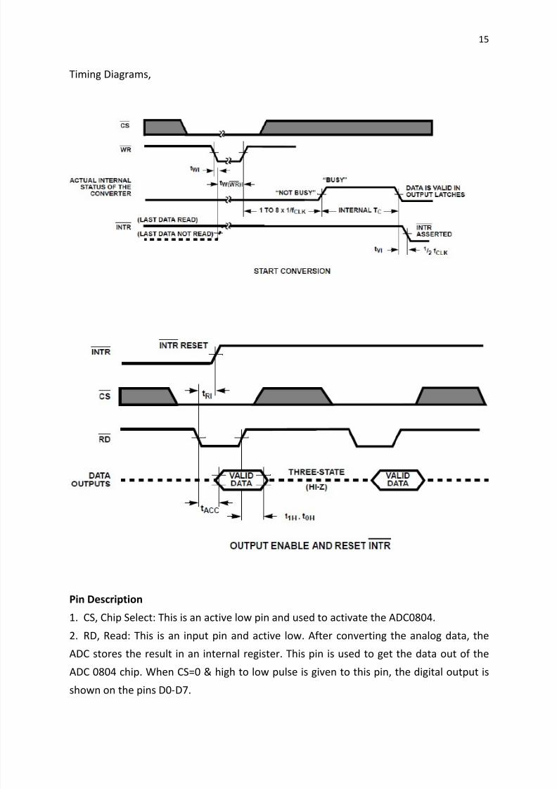
Timing Diagrams,
Pin Description
1. CS, Chip Select: This is an active low pin and used to activate the ADC0804.
2. RD, Read: This is an input pin and active low. After converting the analog data, the
ADC stores the result in an internal register. This pin is used to get the data out of the
ADC 0804 chip. When CS=0 & high to low pulse is given to this pin, the digital output is
shown on the pins D0‐D7.
8/20/2019 Microcontroller Voltmeter
http://slidepdf.com/reader/full/microcontroller-voltmeter 16/28
16
3. WR, Write: This is an input pin and active low. This is used to instruct the ADC to start
the conversion process. If CS=0 and WR makes a low to high transition, the ADC starts
the conversion process.
4.
CLK
IN,
Clock
IN:
This
is
an
input
pin
connected
to
an
external
clock
source.
5. INTR, Interrupt: This is an active low output pin. This pin goes low when the
conversion is over.
6. Vin+ : Analog Input .
7. Vin‐ : Analog Input. Connected to ground.
8. AGND: Analog Ground.
9. Vref/2: This pin is used to set the reference voltage. If this is not connected the
default reference voltage is 5V. In some application it is required to reduce the step size.
This can be done by using this pin.
10. DGND: Digital Ground.
11‐18. Output Data Bits (D7‐D0).
19. CLKR: Clock Reset.
20. Vcc: Positive Supply
The above timing diagrams are from ADC0804 datasheet. The first diagram shows how
to start a conversion. Also you can see which signals are to be asserted and at what time
to start a conversion. So looking into the timing diagram we note down the steps or say the order in which signals are to be asserted to start a conversion of ADC. As we have
decided to make Chip select pin as low so we need not to bother about the CS signal in
the timing diagram. Below steps are for starting an ADC conversion. I am also including
CS signal to give you a clear picture. While programming we will not use this signal.
1. Make chip select (CS) signal low.
2. Make write (WR) signal low.
3. Make chip select (CS) high.
4. Wait for INTR pin to go low (means conversion ends).
Once the conversion in ADC is done, the data is available in the output latch of the ADC.
Looking at the second diagram, which shows the timing diagram of how to read the
converted value from the output latch of the ADC, data of the new conversion is only
available for reading after ADC0804 made INTR pin low or say when the conversion is
over. Below are the steps to read output from the ADC0804.
1. Make chip select (CS) pin low.
2. Make read (RD) signal low.
3.
Read the data from port where ADC is connected.
4.
Make read (RD) signal high. 5.
Make chip select (CS) high.
8/20/2019 Microcontroller Voltmeter
http://slidepdf.com/reader/full/microcontroller-voltmeter 17/28
17
Interfacing the LCD with 8051
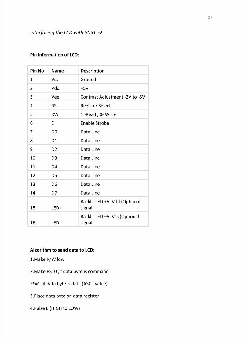
Pin Information of LCD:
Pin No Name Description
1 Vss Ground
2 Vdd +5V
3 Vee Contrast Adjustment ‐2V to ‐5V
4 RS Register Select
5 RW 1 ‐Read , 0‐Write
6 E Enable Strobe
7 D0 Data Line
8 D1 Data Line
9 D2 Data Line
10 D3 Data Line
11 D4 Data Line
12 D5 Data Line
13 D6 Data Line
14 D7 Data Line
15 LED+
Backlit LED +V Vdd (Optional
signal)
16 LED‐
Backlit LED –V Vss (Optional
signal)
Algorithm to send data to LCD:
1.Make R/W low
2.Make RS=0 ;if data byte is command
RS=1 ;if data byte is data (ASCII value)
3.Place data byte on data register
4.Pulse E (HIGH to LOW)
8/20/2019 Microcontroller Voltmeter
http://slidepdf.com/reader/full/microcontroller-voltmeter 18/28
18
5.Repeat the steps to send another data byte
LCD Initialization:
Proper working of LCD depend on the how the LCD is initialized. We have to send few
command bytes to initialize the LCD. Simple steps to initialize the LCD
1. Specify function set: Send 38H for 8‐bit, double line and 5x7 dot character
format.
2. Display On‐Off control: Send 0FH for display and blink cursor on.
3. Entry mode set: Send 06H for cursor in increment position and shift is invisible.
4. Clear display: Send 01H to clear display and return cursor to home position.
Writing software:
The LCD module is an intelligent component. We communicate to LCD module by
sending commands from microcontroller. To write data to LCD module separate
sequence is followed for 4 bit and 8 bit mode.
Writing command for 8 Bit mode:
• Write 8 bit data on D0‐D7
• Generate strobe by taking EN from high to low
•
Writing command for 4 Bit mode:
• Write 4 bit data (upper nibble) on D4‐D7
• Generate strobe by taking EN from high to low
•
Write 4 bit data (lower nibble) on D4‐D7 • Generate strobe by taking EN from high to low
8/20/2019 Microcontroller Voltmeter
http://slidepdf.com/reader/full/microcontroller-voltmeter 19/28
19
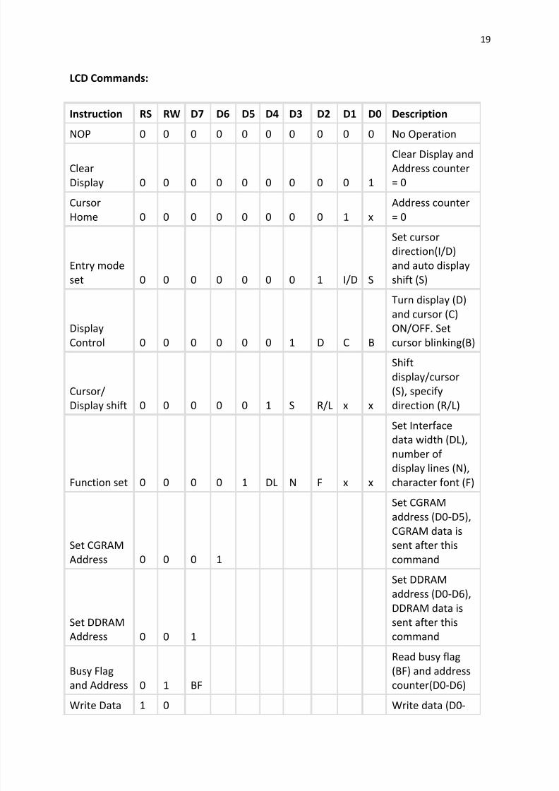
LCD Commands:
Instruction RS RW D7 D6 D5 D4 D3 D2 D1 D0 Description
NOP
0
0
0
0
0
0
0
0
0
0
No Operation
Clear
Display 0 0 0 0 0 0 0 0 0 1
Clear Display and
Address counter
= 0
Cursor
Home 0 0 0 0 0 0 0 0 1 x
Address counter
= 0
Entry mode
set 0 0 0 0 0 0 0 1 I/D S
Set cursor
direction(I/D)
and auto display
shift (S)
Display
Control 0 0 0 0 0 0 1 D C B
Turn display (D)
and cursor (C)
ON/OFF. Set
cursor blinking(B)
Cursor/
Display shift 0 0 0 0 0 1 S R/L x x
Shift
display/cursor
(S), specify
direction (R/L)
Function set 0 0 0 0 1 DL N F x x
Set Interface
data width (DL),
number of
display lines (N),
character font (F)
Set CGRAM
Address 0 0 0 1
Set CGRAM
address (D0‐D5),
CGRAM data is
sent after this
command
Set DDRAM
Address 0 0 1
Set DDRAM
address (D0‐D6),
DDRAM data is
sent after this
command
Busy Flag
and Address 0 1 BF
Read busy flag
(BF) and address
counter(D0‐D6)
Write Data 1 0 Write data (D0‐
8/20/2019 Microcontroller Voltmeter
http://slidepdf.com/reader/full/microcontroller-voltmeter 20/28
20
D7) into
DDRAM/CGRAM
Read Data 1 1
Read data (D0‐
D7) from
DDRAM/CGRAM
Legends used in table:‐
I/D: 1‐ Increment, 0‐ Decrement
S: 1‐ Auto Display shift, 0 – No display shift
D: 1‐ Display ON, 0 – Display OFF
C: 1‐ Cursor ON, 0‐ Cursor OFF
B: 1‐ Cursor blinking ON, 0 – Cursor blinking OFF
S: 1‐ Display Shift, 0 –Cursor move
R/L: 1‐ Shift right, 0‐ Shift left
DL: 1‐ 8 bit interface, 0‐ 4 bit interface
N: 1‐ 2 lines, 0‐ 1 line
F: 1‐ 5X10 dots font, 0‐ 5X7 dots font
BF: Busy Flag
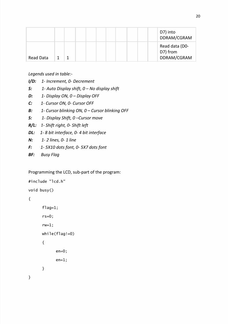
Programming the LCD, sub‐part of the program:
#include "lcd.h"
void busy()
{
flag=1;
rs=0;
rw=1;
while(flag!=0)
{
en=0;
en=1;
}
}
8/20/2019 Microcontroller Voltmeter
http://slidepdf.com/reader/full/microcontroller-voltmeter 21/28
21
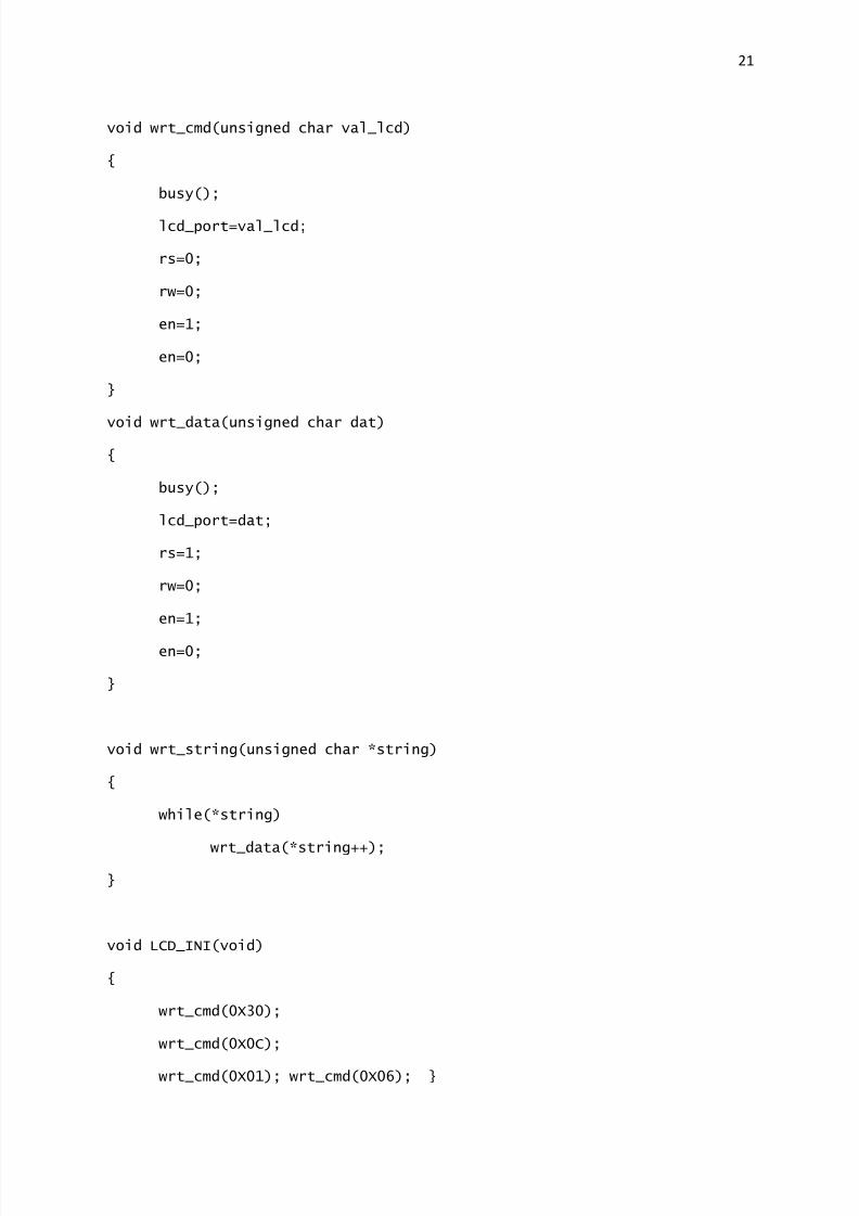
void wrt_cmd(unsigned char val_lcd)
{
busy();
lcd_port=val_lcd;
rs=0;
rw=0;
en=1;
en=0;
}
void wrt_data(unsigned char dat)
{
busy();
lcd_port=dat;
rs=1;
rw=0;
en=1;
en=0;
}
void wrt_string(unsigned char *string)
{
while(*string)
wrt_data(*string++);
}
void LCD_INI(void)
{
wrt_cmd(0X30);
wrt_cmd(0X0C);
wrt_cmd(0X01); wrt_cmd(0X06); }
8/20/2019 Microcontroller Voltmeter
http://slidepdf.com/reader/full/microcontroller-voltmeter 22/28
22
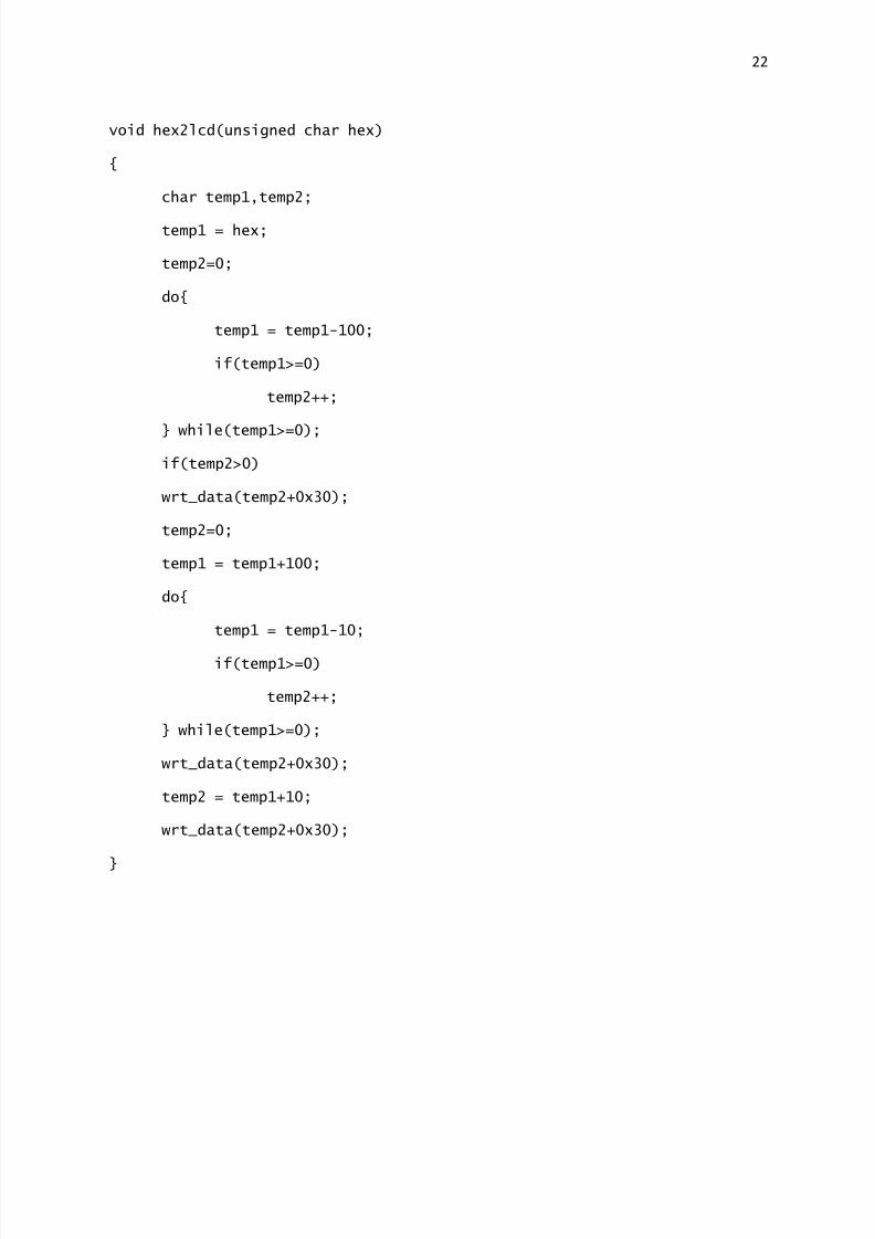
void hex2lcd(unsigned char hex)
{
char temp1,temp2;
temp1 = hex;
temp2=0;
do{
temp1 = temp1-100;
if(temp1>=0)
temp2++;
} while(temp1>=0);
if(temp2>0)
wrt_data(temp2+0x30);
temp2=0;
temp1 = temp1+100;
do{
temp1 = temp1-10;
if(temp1>=0)
temp2++;
} while(temp1>=0);
wrt_data(temp2+0x30);
temp2 = temp1+10;
wrt_data(temp2+0x30);
}

8/20/2019 Microcontroller Voltmeter
http://slidepdf.com/reader/full/microcontroller-voltmeter 23/28
23
Entire Program used for the Digital Voltmeter
#include <REGX51.H>
#include "lcd.h"
#define adc_port P1 //ADC Port
#define rd P3_7 //Read signal P3.7
#define wr P3_6 //Write signal P3.6
#define cs P3_5 //Chip Select P3.5
#define intr P3_4 //INTR signal P3.4
void conv(); //Start of conversion function
void read(); //Read ADC function
unsigned int adc_avg,adc;
void main(){
char i;
LCD_INI();
while(1){ //Forever loop
adc_avg = 0;
for(i=0;i<10;i++){
conv(); //Start conversion
read(); //Read ADC
adc_avg += adc;
}
adc_avg = adc_avg/10;
wrt_cmd(0x80);
wrt_string("V(DC): ");
adc = adc_avg * 59;
8/20/2019 Microcontroller Voltmeter
http://slidepdf.com/reader/full/microcontroller-voltmeter 24/28
24
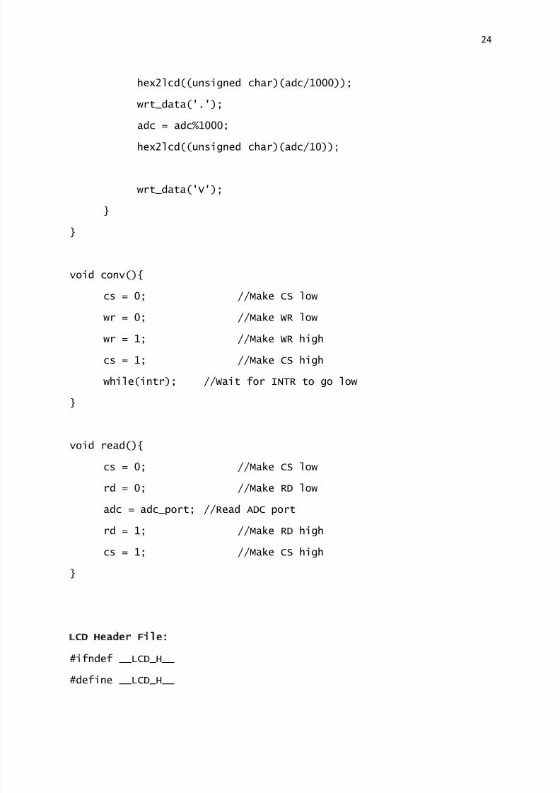
hex2lcd((unsigned char)(adc/1000));
wrt_data('.');
adc = adc%1000;
hex2lcd((unsigned char)(adc/10));
wrt_data('V');
}
}
void conv(){
cs = 0; //Make CS low
wr = 0; //Make WR low
wr = 1; //Make WR high
cs = 1; //Make CS high
while(intr); //Wait for INTR to go low
}
void read(){
cs = 0; //Make CS low
rd = 0; //Make RD low
adc = adc_port; //Read ADC port
rd = 1; //Make RD high
cs = 1; //Make CS high
}
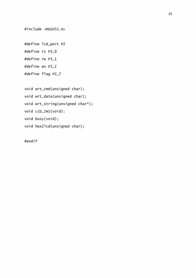
LCD Header File
#ifndef __LCD_H__
#define __LCD_H__
8/20/2019 Microcontroller Voltmeter
http://slidepdf.com/reader/full/microcontroller-voltmeter 25/28
25
#include <REGX51.H>
#define lcd_port P2
#define rs P3_0
#define rw P3_1
#define en P3_2
#define flag P2_7
void wrt_cmd(unsigned char);
void wrt_data(unsigned char);
void wrt_string(unsigned char*);
void LCD_INI(void);
void busy(void);
void hex2lcd(unsigned char);
#endif

8/20/2019 Microcontroller Voltmeter
http://slidepdf.com/reader/full/microcontroller-voltmeter 26/28
26
Theory of the Voltage Calculation in the circuit
All we want is input voltage to ADC should not increase 5V and our maximum input
voltage to voltmeter is 15V only. So we design the voltage divider circuit as follows.
Vmax is Maximum input voltage to voltmeter.
Vip is input voltage to ADC.
R1 and R2 are resistance of voltage divider circuit.
Vmax = 15V
V = R2*Vmax/(R1+R2)
5/15 = R2/R1+R2
3 = R1/R2+1
2 = R1/R2
R2 = R1/2
Let’s take R1 as 200K and R2 will be 100K
Maximum current: Imax = (Vmax‐Vi/pmax)/R1 (approx)
Vmax = 15V
Vi/pmax = 5V
R1 = 200K
Imax = (15‐5)/200 = 10/200 = 0.02mA
8/20/2019 Microcontroller Voltmeter
http://slidepdf.com/reader/full/microcontroller-voltmeter 27/28
27
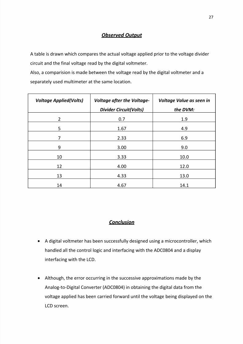
Observed Output
A table is drawn which compares the actual voltage applied prior to the voltage divider
circuit and the final voltage read by the digital voltmeter.
Also, a comparision is made between the voltage read by the digital voltmeter and a
separately used multimeter at the same location.
Voltage Applied(Volts) Voltage after the Voltage‐
Divider Circuit(Volts)
Voltage Value as seen in
the DVM:
2 0.7 1.9
5 1.67 4.9
7 2.33 6.9
9 3.00 9.0
10 3.33 10.0
12 4.00 12.0
13 4.33 13.0
14 4.67 14.1
Conclusion
•
A digital voltmeter has been successfully designed using a microcontroller, which
handled all the control logic and interfacing with the ADC0804 and a display
interfacing with the LCD.
• Although, the error occurring in the successive approximations made by the
Analog‐to‐Digital Converter (ADC0804) in obtaining the digital data from the
voltage applied has been carried forward until the voltage being displayed on the
LCD screen.
8/20/2019 Microcontroller Voltmeter
http://slidepdf.com/reader/full/microcontroller-voltmeter 28/28
28
•
The voltages to be measured limits to a higher value of 14V and DC voltages are
much considerably viewed. Indeed, AC voltages also could be viewed but, the
displayed changes as frequently as the magnitude of the AC voltage is said to
change by its nature.
• Also, the voltage drop across the voltage divider circuit varies, with the
continuous usage of the DVM, and thus a resulting error in the voltage value
might be seen when it’s displayed on the LCD screen.
Advantages
The digital voltmeter designed uses a microcontroller which is said to be highly efficient
in handling the data carrier operation in terms of being faster and being error‐free and
accurate. Thus, it can be considered as a reliable device for observing voltages of
magnitudes from 0 to 14V.
Rather than using the obsolete analogue ways of finding out the voltages, the digital
voltmeter provides much more precise and accurate values of voltages in a given circuit
in the range of the voltmeter.