Embed Size (px)
Citation preview
1
Microcontrollers –
Get to know about them and design
your own projects
2
Table of Contents
Chapter 1: Microcontrollers Page No.
1.1 Introduction to Microcontrollers 9
1.2 Brief about microprocessors 10
1.3 Types of microprocessors 11
1.4 How are microcontrollers different from microprocessors 12
1.5 How are microcontrollers classified? 13
1.5.1 Classification according to number of bits
1.5.2 Classification according to memory devices
1.5.3 Classification according to instruction set
1.5.4 Classification according to memory architecture
1.6 Summary 16
Chapter 2: Microcontroller 8051
2.1 Introduction 17
2.1.1 History
2.2.2 Brief Idea
2.2 8051 Architecture 18
2.3 8051 Pin Description 21
2.4 8051 Application areas 23
2.5 Summary 24
3
Chapter3- AVR Microcontrollers
3.1 Introduction 25
3.1.1 History
3.1.2 How are AVR microcontrollers different from 8051 microcontrollers?
3.1.3 How are AVR microcontrollers classified?
3.2 ATMega328 26
3.2.1 Key Features
3.2.2 Pin Description
3.3 ATMega32 28
3.3.1 Introduction
3.3.2 Key Features
3.3.3 Different sleep modes in ATMega32
3.3.4 Pin Description
3.3.5 Memory Structure
3.4 ATMega8 33
3.4.1 Introduction
3.4.2 ATMega8 architecture
3.4.3 ATMega8 pin description
3.4.4 ATMega8 sleep modes
3.5 Summary 39
4
Chapter 4- PIC Microcontrollers
4.1 Introduction 40
4.1.1 Brief idea about PIC microcontrollers
4.1.2 Key features
4.2 Pin Description of PIC microcontroller 42
4.3 PIC microcontroller architecture 45
4.4 Summary 49
Chapter5- ARM microcontrollers
5.1 Introduction 50
5.1.1 History
5.1.2 ARM usage
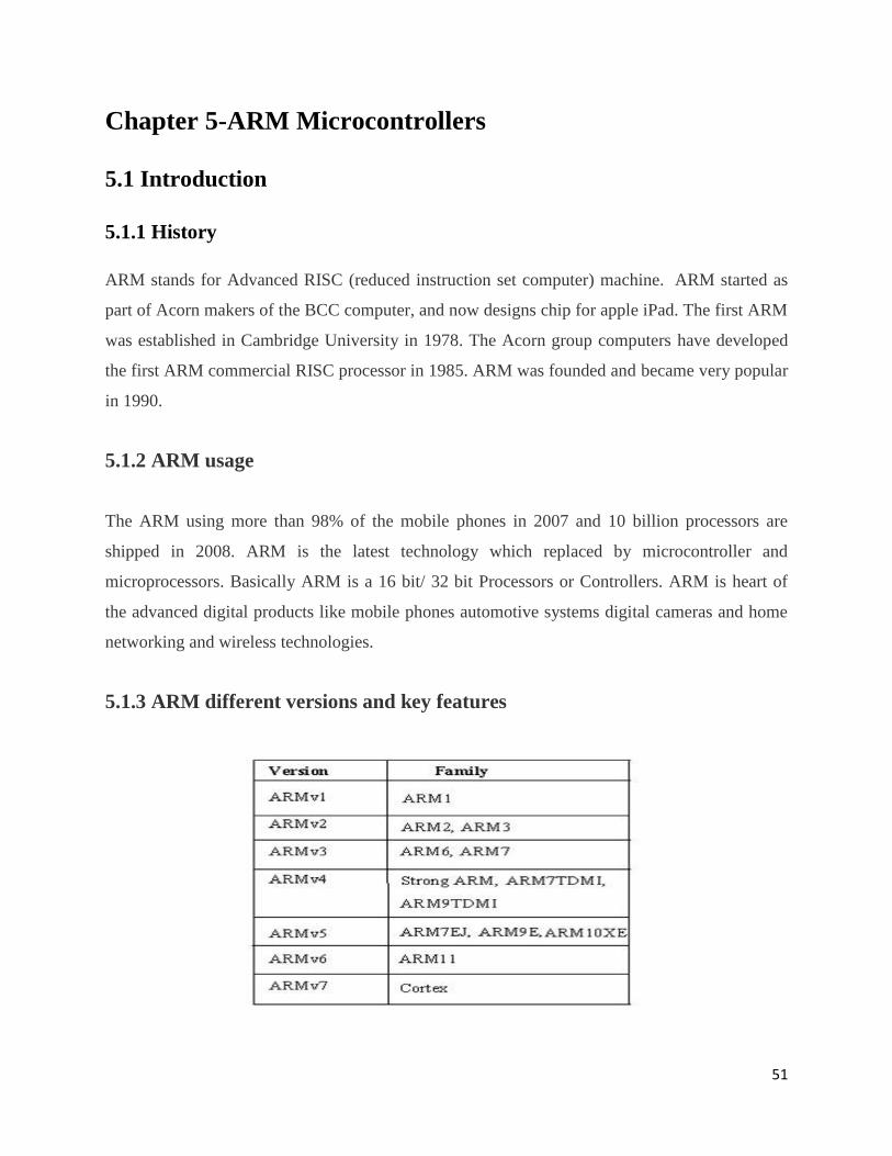
5.1.3 ARM different versions and key features
5.2 ARM architecture 52
5.3 ARM7 54
5.4 Summary 55
5
Chapter 6- Renesas microcontrollers
6.1 Introduction 56
6.2 Pin description 56
6.3 Architecture 57
6.4 Summary 59
Chapter 7- Microcontroller communication
7.1 Introduction 60
7.2 Inter system protocol 60
7.2.1 UART
7.2.2 USART
7.2.3 USB
7.2.4 Difference between inter system protocols
7.3 Intra system protocols 63
7.3.1 I2C protocol
7.3.2 SPI
7.3.3 CAN
7.4 Microcontroller communication with Computers 66
7.4.1 How is microcontrollers interfaced to computers/CPU?
7.4.2 RS232 Cable
6
7.4.3 Max232
7.5 Summary 72
Chapter 8- Programming a microcontroller
8.1 Introduction to programming a microcontroller 73
8.2 Assembly level language programming 73
8.2.1 8051 RAM memory structure
8.2.2 Assembly level language coding
8.2.3 Steps in writing and executing a program
8.3 C Language program 76
8.3.1 Software used in microcontroller program
8.3.2 How to use Kiel software to write microcontroller program?
8.3.3 Steps in developing a microcontroller program
8.4 Summary 84
Chapter 9 – Microcontroller Interfacing
9.1 Microcontroller interfacing with matrix keypad 85
9.1.1 What is matrix keypad?
9.1.2 How is matrix keypad interfaced to 8051 microcontroller?
7
9.2 Motor interfacing to microcontroller 86
9.2.1 Introduction to LM293D-Motor driver IC
9.2.2 How is motor interfaced to 8051 microcontroller?
9.3 Relay interfacing to 8051 microcontroller 88
9.3.1 Introduction to relay drivers
9.3.2 Interfacing relay with microcontroller using ULN2003
9.3.3 Interfacing relay with microcontroller using transistors
9.4 16 by 2 LCD display interfacing with microcontrollers 89
9.5 Summary 91
Chapter 10 – Designing your own microcontroller based projects
10.1 Step by step guide to build your own microcontroller projects 92
10.1.1 Introduction and theory about the project
10.1.2 Step1 - Circuit designing
10.1.3 Step 2- Microcontroller program coding
10.1.4 Step 3- Circuit drawing
10.1.5 Step 4 – Code dumping
10.1.6 Step 5- Simulating the circuit
10.2 Few microcontroller based projects 100
8
10.2.1 Controlling loads using microcontroller
10.2.2 Motor speed control using microcontroller
10.2.3 GSM based monthly energy meter billing using microcontroller
10.2.4 Automatic dialing to any telephone on detecting burglary
10.3 Few microcontroller based circuits 105
10.3.1 Lamp switching using PIC microcontroller
10.3.2 Programmed message sending circuit
10.3.3 Intra system communication in automobiles
10.4 Summary 108
Ending Stuff 109
About the authors
Rights to readers
Legal Info
Ways to interact
9
Chapter 1- Microcontrollers
1.1. Introduction to Microcontrollers
A microcontroller is a small, low-cost and self contained computer-on-a-chip that can be used as
an embedded system. It is a computer on‐a‐chip optimized to manage electric gadgets. It is
intended particularly for precise tasks like controlling a particular system. A micro-controller can
be abbreviated as µC, or MCU.
Also, a micro-controller is a fraction of a fixed in system, which is fundamentally a complete
circuit board. A fixed-in system is a computer system intended to carry out one or more
functions over and over again with real‐time work out limits. It is embedded as an element of a
full machine often counting hardware and motorized elements as well.
Examples of micro-controllers are the 8051, Intel’s 80196, Microchip’s PIC and Motorola’s
68HCxx series. Micro-controllers which are normally incorporated in toys, automobiles,
appliances and office machines are gears which amalgamate a number of constituents of a micro-
processor system on a solo microchip.
A few microcontrollers may utilize four-bit expressions and work at clock rate frequencies,
which usually include:
An 8 or 16 bit microprocessor.
A little measure of RAM.
Programmable ROM and flash memory.
Parallel and serial I/O.
Timers and signal generators.
10
Analog to Digital and Digital to Analog conversion
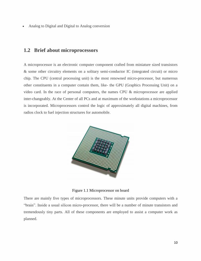
1.2 Brief about microprocessors
A microprocessor is an electronic computer component crafted from miniature sized transistors
& some other circuitry elements on a solitary semi-conductor IC (integrated circuit) or micro
chip. The CPU (central processing unit) is the most renowned micro-processor, but numerous
other constituents in a computer contain them, like- the GPU (Graphics Processing Unit) on a
video card. In the race of personal computers, the names CPU & microprocessor are applied
inter-changeably. At the Center of all PCs and at maximum of the workstations a microprocessor
is incorporated. Microprocessors control the logic of approximately all digital machines, from
radios clock to fuel injection structures for automobile.
Figure 1.1 Microprocessor on board
There are mainly five types of microprocessors. These minute units provide computers with a
“brain”. Inside a usual silicon micro-processor, there will be a number of minute transistors and
tremendously tiny parts. All of these components are employed to assist a computer work as
planned.
11
1.2.1 Types of Microprocessors
Complex Instruction Set Microprocessors:
This type of microprocessor is also known as CISM. CISM classify a micro-processor in which
each & every order can be executed together with several other low-level functions. These
functions are intended to carry out actions such as- uploading data into memory card, re-calling
or downloading data from memory card or a complex mathematics computation in a single
command.
Reduced Instruction Set Microprocessors:
Also known as RISC, this was intended to pace up computer microprocessors. These chips are
built up under the guideline that permits the microprocessor to do a smaller amount of things
within each command and this will permit it to complete more commands more rapidly.
Superscalar processors:
These types of processors resemble the hardware on the micro-processor so that it can perform
numerous instructions at the same time. These replica resources can be committed arithmetic
logic units or multipliers. Super scalars comprise of several operational units. Superscalar micro-
processors carry out more than one command throughout a single clock cycle by concurrently
transmitting numerous instructions to superfluous operational units in the processor.
The Application Specific Integrated Circuit:
Also known as ASIC microprocessor is intended for extremely precise purposes, which possibly
will comprise- automotive emissions control or Personal Digital Assistants computers. ASICs at
times is produced to specification, but can also be manufactured by making use of off-the-shelf
gears.
12
Digital Signal Multiprocessors (DSPs):
DSPs are unique micro-processors employed to decode & encode video, or convert digital or
video to analog and vice-versa. These operations need a micro-processor particularly excellent at
carrying out mathematical calculations. DSP chips are generally employed in SONAR, mobile
telephones, RADAR, home theater audio gears and cable set-top boxes.
1.3 How are microcontrollers different from microprocessors?
The dissimilarity between the two is that a micro-controller integrates the features of a
microprocessor (ALU, CPU, Registers) together with the existence of extra characteristics such
as existence of ROM, RAM, counter, Input/ Output ports, etc. On the contrary, a micro-
controller controls the function of a device by employing fixed programs accumulated in ROM
that does no amend with duration.
From one more point of view, the major dissimilarity amid a usual micro-processor and a micro
controller parting there architectural terms is the area of their application. Usual microprocessors
such as the Pentium family or Intel Core family processors or alike processors are in computers
as a universally functioning programmable machine. In its life span it has to manage numerous
different assignments and programs specified to it. In contrast a micro-controller of PIC family
or 8051 family or any other have noticed their applications in tiny embedded systems such as-
control system of traffic signals or some sort of robotic system. Also these gadgets manage
similar task or similar program all through their entire life cycle.
Another difference is that the microcontroller generally has to handle instantaneous tasks
whereas on the contrary the micro-processors in a computer system perhaps will not handle an
instantaneous task at all times.
13
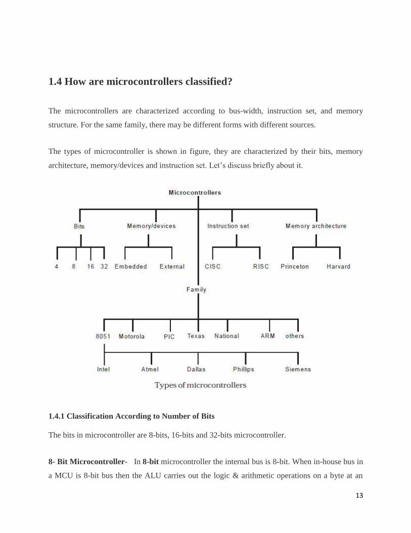
1.4 How are microcontrollers classified?
The microcontrollers are characterized according to bus-width, instruction set, and memory
structure. For the same family, there may be different forms with different sources.
The types of microcontroller is shown in figure, they are characterized by their bits, memory
architecture, memory/devices and instruction set. Let’s discuss briefly about it.
1.4.1 Classification According to Number of Bits
The bits in microcontroller are 8-bits, 16-bits and 32-bits microcontroller.
8- Bit Microcontroller- In 8-bit microcontroller the internal bus is 8-bit. When in-house bus in
a MCU is 8-bit bus then the ALU carries out the logic & arithmetic operations on a byte at an
14
order. The MCU is 8-bit micro-controller. The examples of 8-bit microcontrollers are Intel
8031/8051, PIC1x and Motorola MC68HC11 families.
16 bit Microcontroller- A 16 bit Microcontroller consists of a 16 bit bus and the ALU performs
arithmetic and logic operations on the 16 bit operand. It provides greater precision and
performance as compared to 8 bit MCU.
For example 8 bit microcontrollers can only use 8 bits, resulting in a final range of 0×00 – 0xFF
(0-255) for every cycle. In contrast, 16 bit microcontrollers with its 16 bit data width has a range
of 0×0000 – 0xFFFF (0-65535) for every cycle. A longer timer most extreme worth can likely
prove to be useful in certain applications and circuits. It can automatically operate on two 16 bit
numbers. Some examples of 16-bit microcontroller are 16-bit MCUs are extended 8051XA,
PIC2x, Intel 8096 and Motorola MC68HC12 families.
32 bit microcontroller- The 32-bit microcontroller uses the 32-bit instructions to perform the
arithmetic and logic operations. When in-house bus for the data transmitting function in an MCU
is 32-bit bus then the ALU carries out logic & arithmetic functions on operand words of 32 bits
at the orders. The MCU is 32-bit micro-controller. These supply better accuracy and
performance in comparison to the 16-bit MCUs.
These are used in automatically controlled devices including implantable medical devices,
engine control systems, office machines, appliances and other types of embedded systems. Some
examples are Intel/Atmel 251 family, PIC3x.
1.4.2 Classification According to Memory Devices
The memory devices are divided into two types, they are
Embedded memory microcontroller: When an embedded system has a microcontroller unit
that has all the functional blocks available on a chip is called an embedded microcontroller. It
has hardware and software embedded into a single unit. . Extremely few or no extra peripheral
unit or system exists for processing during the control or making use of the peripheral d For
15
example, 8051 having program & data memory, I/O ports, serial communication, counters and
timers and interrupts on the chip is an embedded microcontroller.
External Memory Microcontroller: When an embedded system has a microcontroller unit that
has not all the functional blocks available on a chip, it is called an external memory
microcontroller. It has memory externally interfaced to the hardware. It is also known as
peripheral memory. For example, 8031 has no program memory on the chip is an external
memory microcontroller. An 8031 microcontroller comprises of a program memory which is
interfaced outwardly to it.
1.4.3 Classification According to Instruction Set
CISC: CISC is a Complex Instruction Set Computer. It allows the programmer to use one
instruction in place of many simpler instructions.
RISC: The RISC is stands for Reduced Instruction set Computer; this type of instruction sets
reduces the design of microprocessor for industry standards. It allows each instruction to operate
on any register or use any addressing mode and simultaneous access of program and data.
Example for CISC and RISC:
CISC: Mov AX, 4 RISC:
Mov AX, 0
Mov BX, 2
Mov BX, 4
ADD BX, AX
Mov CX, 2
Begin ADD AX, BX
Loop Begin
From above example, RISC systems shorten execution time by reducing the clock cycles per
instruction and CISC systems shorten execution time by reducing the number of instructions per
program. The RISC gives a better execution than the CISC.
16
1.4.4 Classification According to Memory Architecture
Memory architecture of microcontroller are two types, they are namely:
Harvard Memory Architecture Microcontroller: In this type of architecture, the
microcontroller has different memory for program instructions and data. It consists of two
separate buses for instructions and data.
Von Neumann Memory Architecture Microcontroller: In this type of architecture, the
microcontroller has same memory for program instructions and data. It consist of only one bus to
carry both instructions and data.
1.5 Summary
Microcontrollers are digital integrated chips which contain the processor as well as the memory
embedded on the same chip. They are mostly used in embedded systems. Microcontrollers differ
from microprocessors in their architecture as well as their functioning. Different microcontrollers
can be classified based on the number of instruction bits, memory architecture, and instruction
set architecture and memory devices.
17
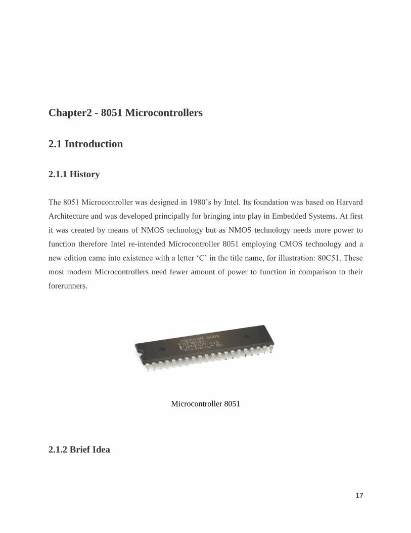
Chapter2 - 8051 Microcontrollers
2.1 Introduction
2.1.1 History
The 8051 Microcontroller was designed in 1980’s by Intel. Its foundation was based on Harvard
Architecture and was developed principally for bringing into play in Embedded Systems. At first
it was created by means of NMOS technology but as NMOS technology needs more power to
function therefore Intel re-intended Microcontroller 8051 employing CMOS technology and a
new edition came into existence with a letter ‘C’ in the title name, for illustration: 80C51. These
most modern Microcontrollers need fewer amount of power to function in comparison to their
forerunners.
Microcontroller 8051
2.1.2 Brief Idea
18
There are two buses in 8051 Microcontroller -one for program and other for data. As a result, it
has two storage rooms for both program and data of 64K by 8 sizes. The microcontroller
comprises of 8 bit accumulator & 8 bit processing unit. It also consists of 8 bit B register as
majorly functioning blocks. It also has a number of other 8 bit and 16 bit registers.
For internal functioning & processing, microcontroller 8051 comes with integrated built-in
RAM. This is prime memory and is employed for storing temporary data. It is unpredictable
memory i.e. its data can get be lost when the power supply to the microcontroller is switched
OFF.
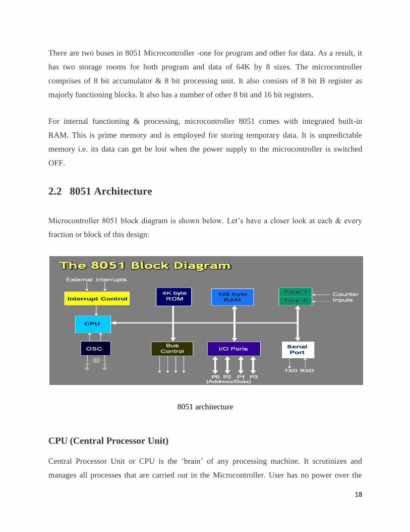
2.2 8051 Architecture
Microcontroller 8051 block diagram is shown below. Let’s have a closer look at each & every
fraction or block of this design:
8051 architecture
CPU (Central Processor Unit)
Central Processor Unit or CPU is the ‘brain’ of any processing machine. It scrutinizes and
manages all processes that are carried out in the Microcontroller. User has no power over the
19
functioning of CPU. It interprets all program instructions stored in storage space (ROM) and
carries out all of them and does the projected duty.
Interrupts
Interrupt is a sub-routine call that reads the Microcontroller’s key function or job and helps it to
perform some other program which is extra important at that point of time. The characteristic of
Interrupt is extremely constructive as it aids in emergency cases. Interrupts provides us a method
to postpone or delay the current process, carry out a sub-routine task and then all over again
restart standard program implementation.
The Micro-controller 8051 can be assembled in such a manner that it momentarily stops or break
the core program at the happening of interrupt. When sub-routine task is finished then the
implementation of core program initiates automatically as usual. There are 5 interrupt supplies in
8051 Microcontroller, two out of five are peripheral interrupts, two are timer interrupts and one
is serial port interrupt.
Memory
Micro-controller needs a program which is a set of commands. This program enlightens
Microcontroller to perform precise tasks. These programs need a storage space on which they
can be accumulated and implemented by microcontroller to act upon any specific process. The
memory which is brought into play to accumulate the program of Microcontroller is recognized
as Program memory or code memory. In common language it’s also known as Read Only
Memory or ROM.
Micro-controller also needs a memory to amass data or operands for the short term. The storage
space which is employed for momentarily data storage is known as Data Memory and we
employ Random Access Memory or RAM for this principle reason. Microcontroller 8051
contains code memory or program memory 4K so that is has 4KB Rom and it also comprise of
data memory (RAM) of 128 bytes.
20
Bus
Fundamentally, Bus is a group of wires which functions as a communication canal or mean for
the transfer Data. These buses comprise of 8, 16 or more cables. As a result, a bus can bear 8
bits, 16 bits all together. There are two types of buses:
1. Address Bus:
Microcontroller 8051 consists of 16 bit address bus. It is brought into play to address memory
positions. It is also utilized to transmit the address from Central Processing Unit to Memory.
2. Data Bus:
Microcontroller 8051 comprise of 8 bits data bus. It is employed to cart data.
Oscillator
As we all make out that Microcontroller is a digital circuit piece of equipment, thus it needs
timer for its function. For this function, Microcontroller 8051 consists of an on-chip oscillator
which toils as a time source for CPU (Central Processing Unit). As the productivity thumps of
oscillator are steady as a result, it facilitates harmonized employment of all pieces of 8051
Microcontroller.
Input/output Port
A microcontroller is employed in embedded systems to manage the functions of devices. Thus to
gather it to other machinery, gadgets or peripherals we need I/O (input/output) interfacing ports
in Micro-controller. For this function Micro-controller 8051 consists of 4 input/output ports to
unite it to other peripherals.
21
Timers/Counters
Micro-controller 8051 is incorporated with two 16 bit counters & timers. The counters are
separated into 8 bit registers. The timers are utilized for measuring the intervals, to find out pulse
width etc.
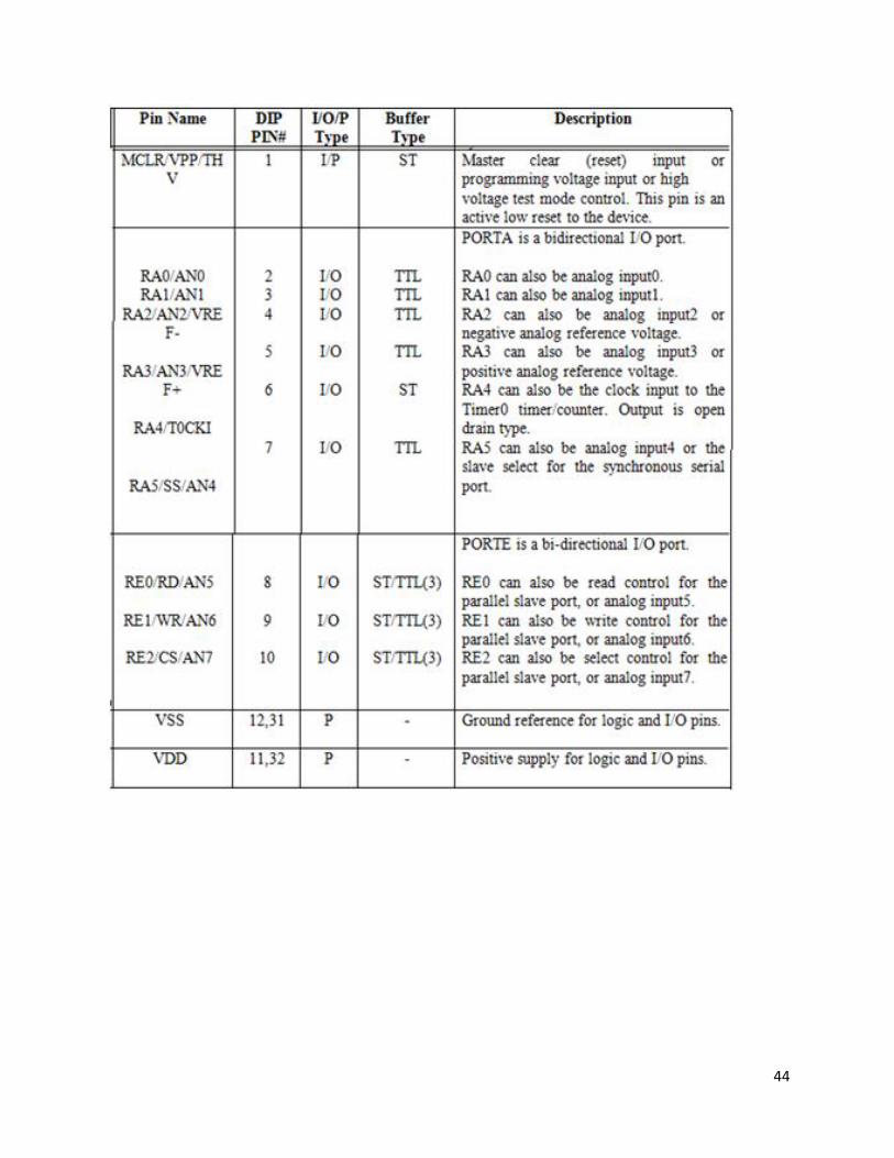
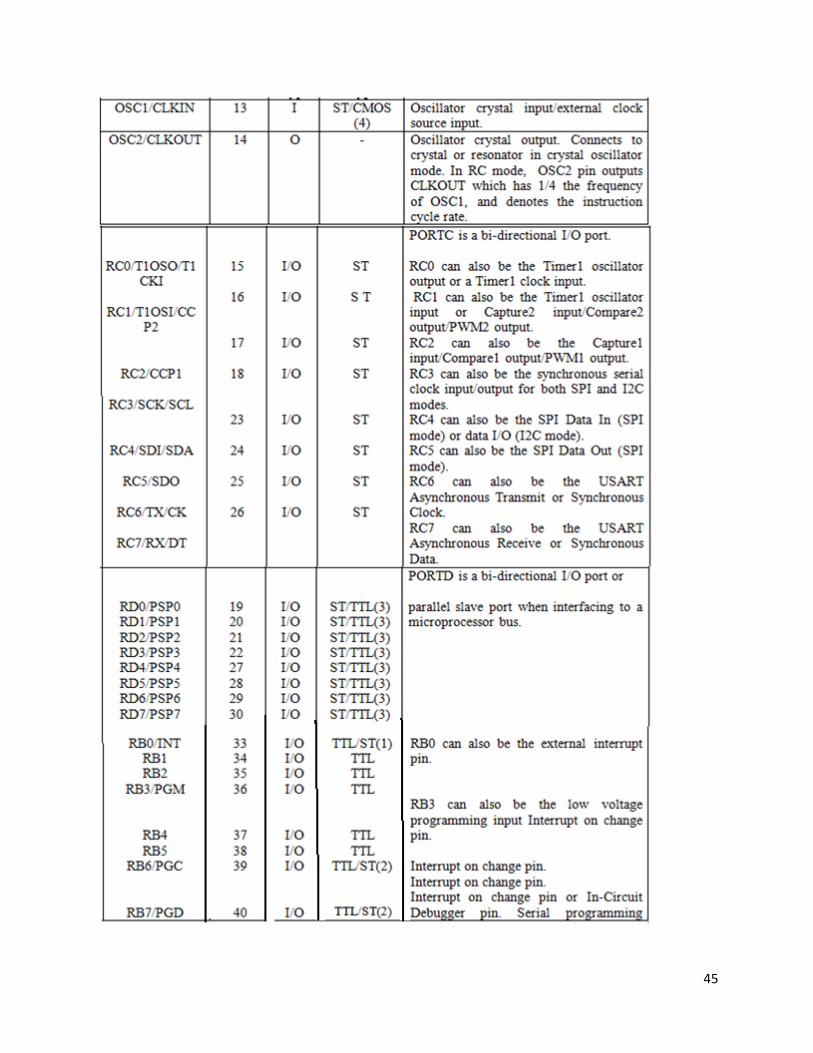
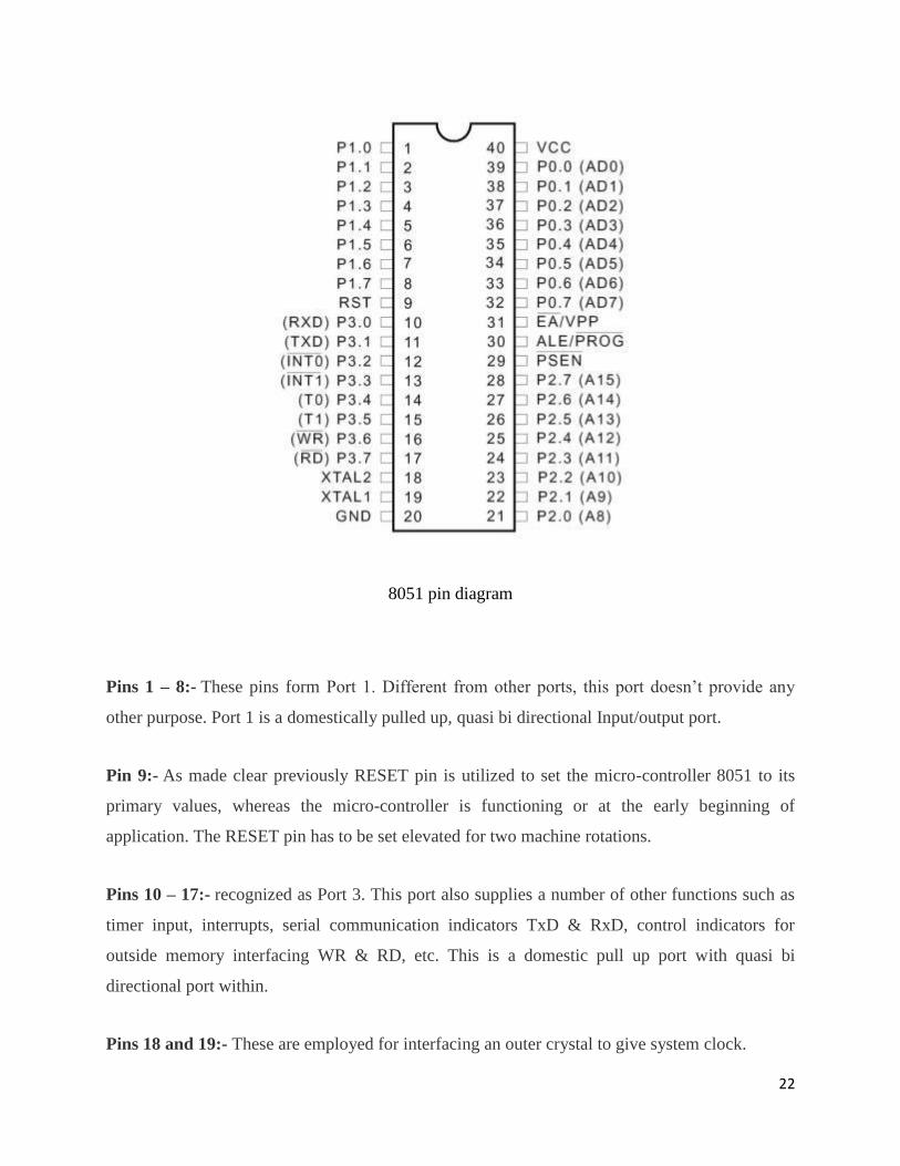
2.3 8051 Pin descriptions
For explaining the pin diagram and pin configuration of microcontroller 8051, we are taking into
deliberation a 40 pin Dual inline package (DIP). Now let’s study through pin configuration in
brief:-
22
8051 pin diagram
Pins 1 – 8:- These pins form Port 1. Different from other ports, this port doesn’t provide any
other purpose. Port 1 is a domestically pulled up, quasi bi directional Input/output port.
Pin 9:- As made clear previously RESET pin is utilized to set the micro-controller 8051 to its
primary values, whereas the micro-controller is functioning or at the early beginning of
application. The RESET pin has to be set elevated for two machine rotations.
Pins 10 – 17:- recognized as Port 3. This port also supplies a number of other functions such as
timer input, interrupts, serial communication indicators TxD & RxD, control indicators for
outside memory interfacing WR & RD, etc. This is a domestic pull up port with quasi bi
directional port within.
Pins 18 and 19:- These are employed for interfacing an outer crystal to give system clock.
23
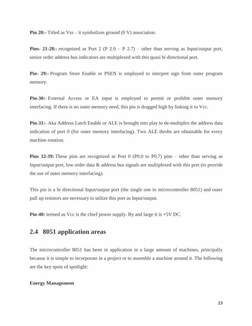
Pin 20:- Titled as Vss – it symbolizes ground (0 V) association.
Pins- 21-28:- recognized as Port 2 (P 2.0 – P 2.7) – other than serving as Input/output port,
senior order address bus indicators are multiplexed with this quasi bi directional port.
Pin- 29:- Program Store Enable or PSEN is employed to interpret sign from outer program
memory.
Pin-30:- External Access or EA input is employed to permit or prohibit outer memory
interfacing. If there is no outer memory need, this pin is dragged high by linking it to Vcc.
Pin-31:- Aka Address Latch Enable or ALE is brought into play to de-multiplex the address data
indication of port 0 (for outer memory interfacing). Two ALE throbs are obtainable for every
machine rotation.
Pins 32-39: These pins are recognized as Port 0 (P0.0 to P0.7) pins – other than serving as
Input/output port, low order data & address bus signals are multiplexed with this port (to provide
the use of outer memory interfacing).
This pin is a bi directional Input/output port (the single one in microcontroller 8051) and outer
pull up resistors are necessary to utilize this port as Input/output.
Pin-40: termed as Vcc is the chief power supply. By and large it is +5V DC.
2.4 8051 application areas
The microcontroller 8051 has been in application in a large amount of machines, principally
because it is simple to incorporate in a project or to assemble a machine around it. The following
are the key spots of spotlight:
Energy Management
24
Competent measuring device systems aid in calculating energy consumption in domestic and
industrialized applications. These meter systems are prepared competent by integrating
microcontrollers.
Touch screens
A high degree of microcontroller suppliers integrate touch sensing abilities in their designs.
Transportable devices such as media players, gaming devices & cell phones are some
illustrations of micro-controller integrated with touch sensing screens.
Automobiles
The microcontroller 8051 discovers broad recognition in supplying automobile solutions. They
are extensively utilized in hybrid motor vehicles to control engine variations. In addition,
works such as cruise power and anti-brake mechanism has created it more capable with the
amalgamation of micro-controllers.
Medical Devices
Handy medicinal gadgets such as glucose & blood pressure monitors bring into play micro-
controllers, to put on view the measurements, as a result, offering higher dependability in
giving correct medical results.
2.5 Summary
8051 Microcontroller is a 40 pin, 8 bit microcontroller based on Harvard architecture wherein the
program memory and data memory are different. The 8051 microcontroller consists of four Input
/ Output ports out of which one port pins can also be used as interrupt pins. The microcontroller
works with an oscillator frequency of 11MHz.
25
Chapter 3- AVR Microcontrollers
3.1 Introduction
3.1.1 History
AVR microcontroller was developed by Alf-Egil Bogen and Vegard Wollan from Atmel
Corporation. The AVR microcontrollers are based on modified Harvard RISC architecture with
separate memories for data and program and speed of AVR are high when compared to 8051 and
PIC. The AVR is stands for Alf-Egil Bogen and Vegard Wollan’s RISC processor.
26
3.1.2 How are AVR microcontrollers different from 8051 microcontrollers?
8051s are 8-bit controllers based on CISC architecture, AVRs are 8-bit controllers based on
RISC architecture
8051 consumes more power than AVR microcontroller
In 8051, we can program easily than the AVR microcontroller
The speed of AVR is more than the 8051 microcontroller
3.1.3 How are AVR microcontrollers classified?
AVR Microcontrollers are classified into three types:
Tiny AVR – Less memory, small size, suitable only for simpler applications
Mega AVR – These are the most popular ones having good amount of memory (up to 256
KB), higher number of inbuilt peripherals and suitable for moderate to complex applications
Xmega AVR – Used commercially for complex applications, which require large program
memory and high speed
27
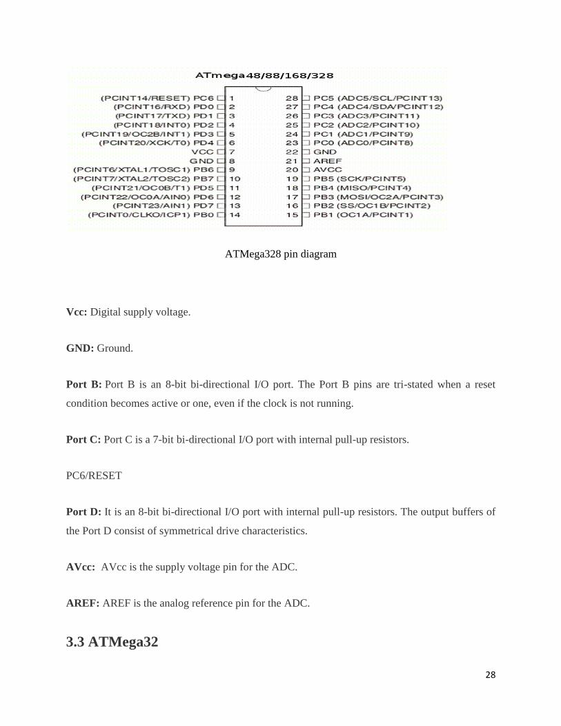
3.2 ATMega328
3.2.1 Key Features
28-pin AVR microcontroller
Flash program memory of 32kbytes
EEPROM data memory of 1kbytes
SRAM data memory of 2kbytes
I/O pins are 23
Two 8-bit timers
A/D converter
Six channel PWM
In built USART
External Oscillator: up to 20MHz
3.2.2 Pin Description
28
ATMega328 pin diagram
Vcc: Digital supply voltage.
GND: Ground.
Port B: Port B is an 8-bit bi-directional I/O port. The Port B pins are tri-stated when a reset
condition becomes active or one, even if the clock is not running.
Port C: Port C is a 7-bit bi-directional I/O port with internal pull-up resistors.
PC6/RESET
Port D: It is an 8-bit bi-directional I/O port with internal pull-up resistors. The output buffers of
the Port D consist of symmetrical drive characteristics.
AVcc: AVcc is the supply voltage pin for the ADC.
AREF: AREF is the analog reference pin for the ADC.
3.3 ATMega32
29
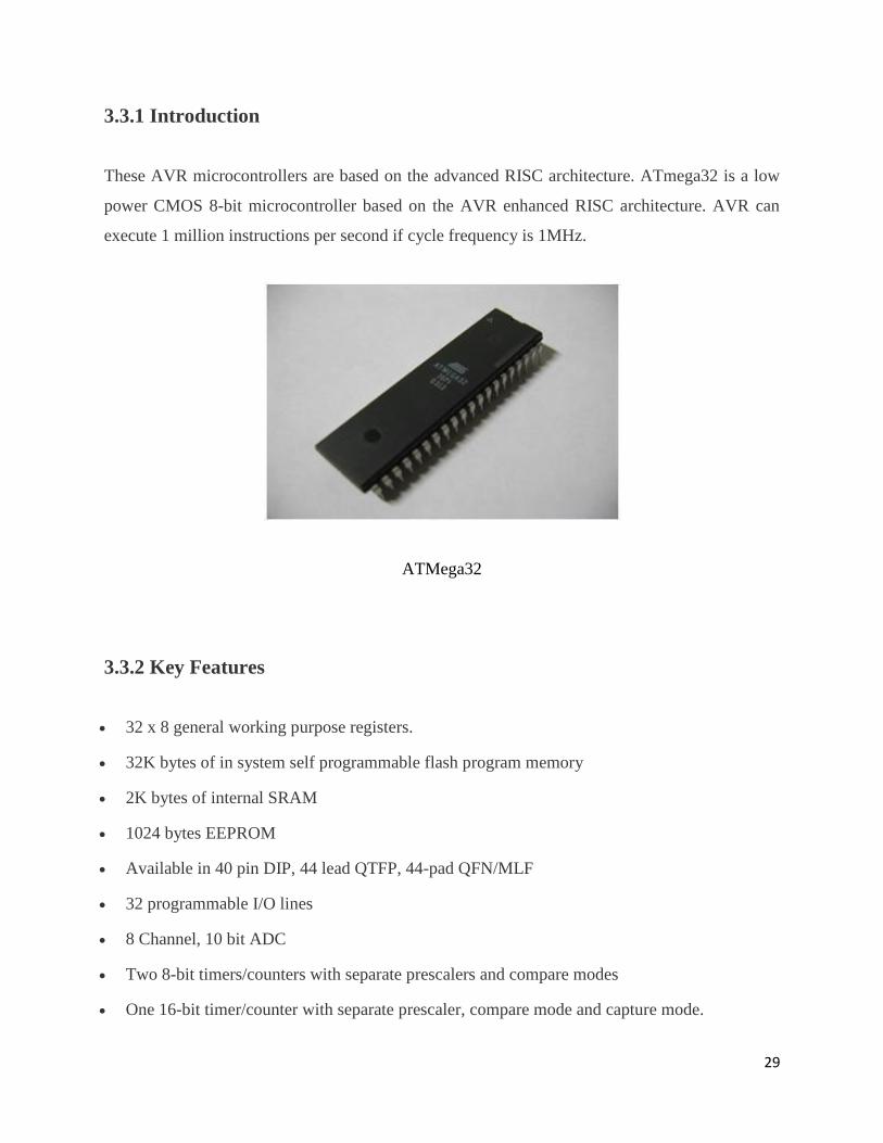
3.3.1 Introduction
These AVR microcontrollers are based on the advanced RISC architecture. ATmega32 is a low
power CMOS 8-bit microcontroller based on the AVR enhanced RISC architecture. AVR can
execute 1 million instructions per second if cycle frequency is 1MHz.
ATMega32
3.3.2 Key Features
32 x 8 general working purpose registers.
32K bytes of in system self programmable flash program memory
2K bytes of internal SRAM
1024 bytes EEPROM
Available in 40 pin DIP, 44 lead QTFP, 44-pad QFN/MLF
32 programmable I/O lines
8 Channel, 10 bit ADC
Two 8-bit timers/counters with separate prescalers and compare modes
One 16-bit timer/counter with separate prescaler, compare mode and capture mode.
30
4 PWM channels
In system programming by on-chip boot program
Programmable watch dog timer with separate on-chip oscillator.
Programmable serial USART
Master/slave SPI serial interface
Six sleep modes: Idle, ADC noise reduction, power-save, power-down, standby and extended
standby.
Internal calibrated RC oscillator
External and internal interrupt sources
Power on reset and programmable brown-out detection.
3.3.3 Different sleep modes in ATMega32
Power down mode- The power-down saves the register contents but freezes the oscillator. All
other chip functions will be disabled until the next external interrupt arises. Asynchronous timer
allows the user to maintain a timer based in power-save mode while the rest of the device is
sleeping.
AC Noise reduction mode- ADC noise reduction mode stops the CPU and all I/O modules
except ADC and asynchronous timer.
Standby mode- In standby mode, except crystal oscillator the rest of the device is sleeping. Both
the main oscillator and asynchronous timer continue to run in extended standby mode.
3.3.4 Pin Description of ATMega32
31
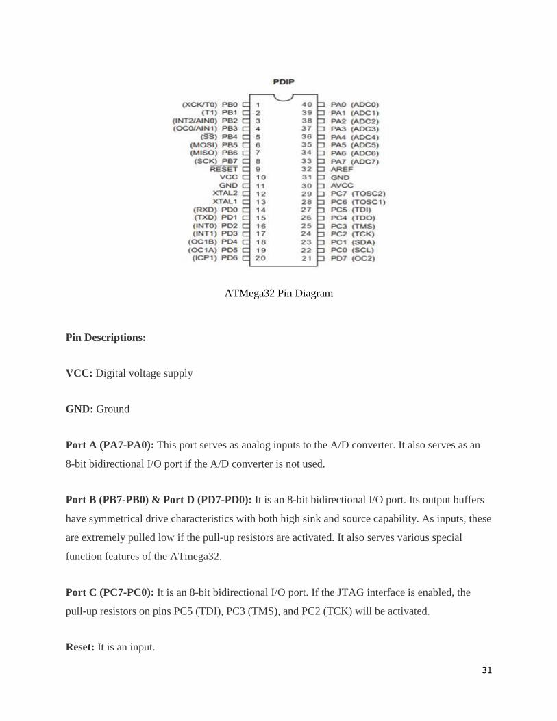
ATMega32 Pin Diagram
Pin Descriptions:
VCC: Digital voltage supply
GND: Ground
Port A (PA7-PA0): This port serves as analog inputs to the A/D converter. It also serves as an
8-bit bidirectional I/O port if the A/D converter is not used.
Port B (PB7-PB0) & Port D (PD7-PD0): It is an 8-bit bidirectional I/O port. Its output buffers
have symmetrical drive characteristics with both high sink and source capability. As inputs, these
are extremely pulled low if the pull-up resistors are activated. It also serves various special
function features of the ATmega32.
Port C (PC7-PC0): It is an 8-bit bidirectional I/O port. If the JTAG interface is enabled, the
pull-up resistors on pins PC5 (TDI), PC3 (TMS), and PC2 (TCK) will be activated.
Reset: It is an input.
32
XTAL1: It is an input to the inverting oscillator amplifier and input to the internal clock
operating circuit.
XTAL2: It is an output from the inverting oscillator amplifier.
AVCC: It is the supply voltage pin for Port A and A/D converter. It should be connected to
VCC.
AREF: AREF is the analog reference pin for the A/D converter.
3.3.5 ATMega32 memory structure
In System Programmable Flash Program Memory:
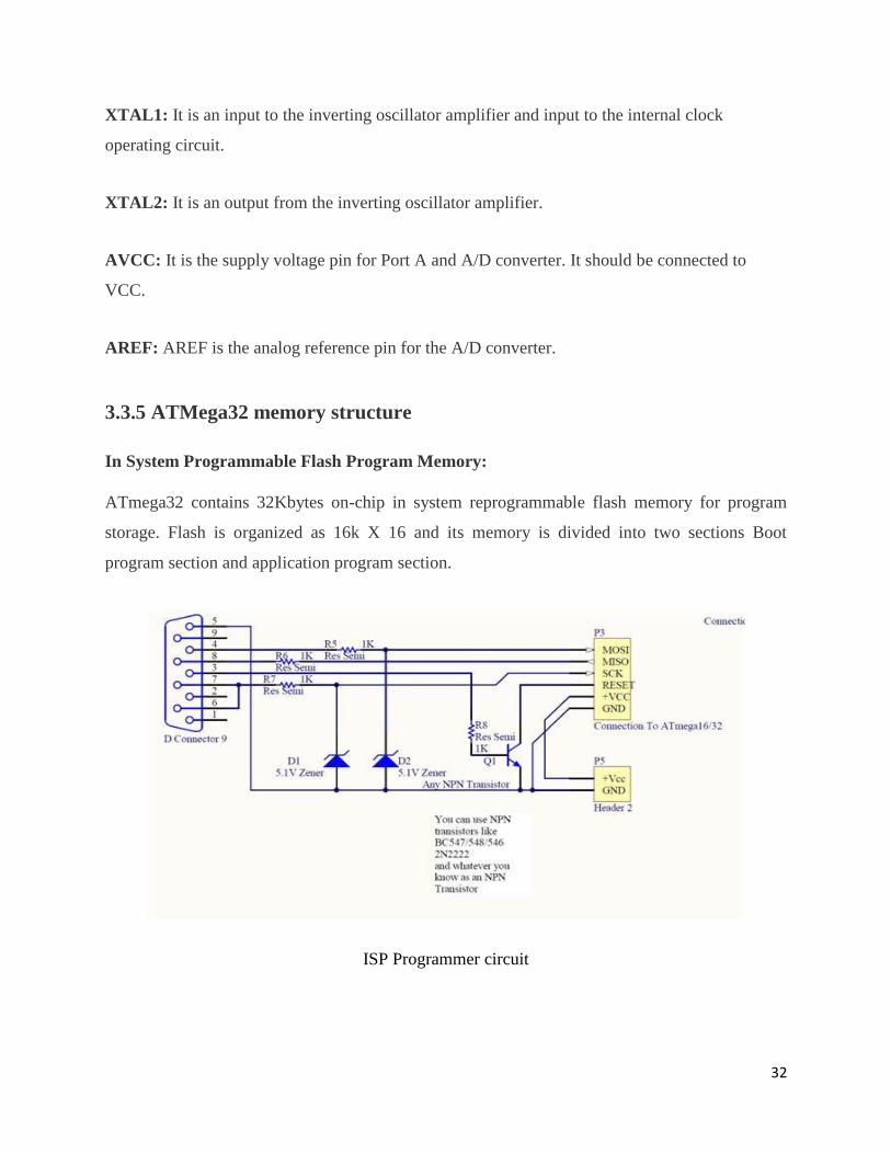
ATmega32 contains 32Kbytes on-chip in system reprogrammable flash memory for program
storage. Flash is organized as 16k X 16 and its memory is divided into two sections Boot
program section and application program section.
ISP Programmer circuit
33
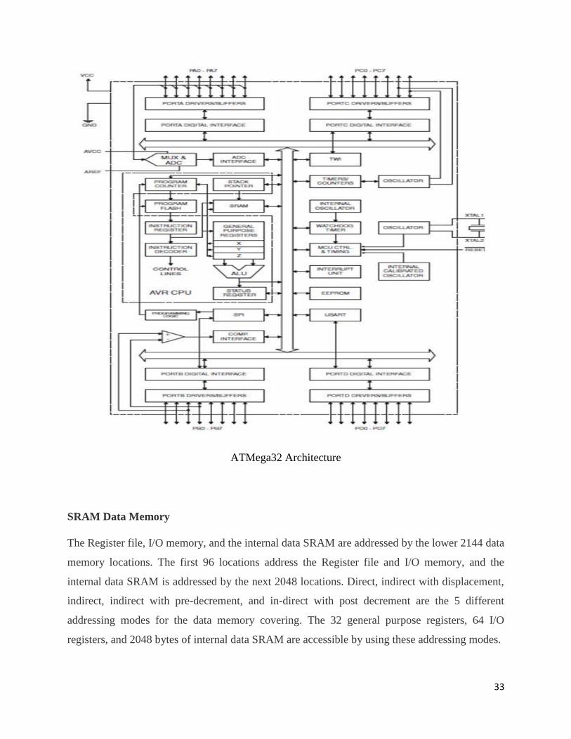
ATMega32 Architecture
SRAM Data Memory
The Register file, I/O memory, and the internal data SRAM are addressed by the lower 2144 data
memory locations. The first 96 locations address the Register file and I/O memory, and the
internal data SRAM is addressed by the next 2048 locations. Direct, indirect with displacement,
indirect, indirect with pre-decrement, and in-direct with post decrement are the 5 different
addressing modes for the data memory covering. The 32 general purpose registers, 64 I/O
registers, and 2048 bytes of internal data SRAM are accessible by using these addressing modes.
34
EEPROM Data Memory
It contains 1024 bytes of data EEPROM memory. It can be accessed as a separate data space in
which single bytes can be read and written.
I/O Memory:
All I/Os and peripherals are placed in the I/O space. The I/O locations are accessed by the IN and
OUT instructions, transferring the data between the 32 general purpose registers and the I/O
space. I/O registers with in the address 00-1F are directly bit accessible using the SBI and CBI
instructions.
3.4 ATMega8
3.4.1 Introduction
It is an 8 bit CMOS built microcontroller from the AVR family (developed by Atmel
Corporation in 1996) and is built on the RSIC (Reduced Instruction Set Computer) architecture.
Its basic advantage is it doesn’t contain any accumulator and the result of any operation can be
stored in any register, defined by the instruction.
ATMega8 Microcontroller
35
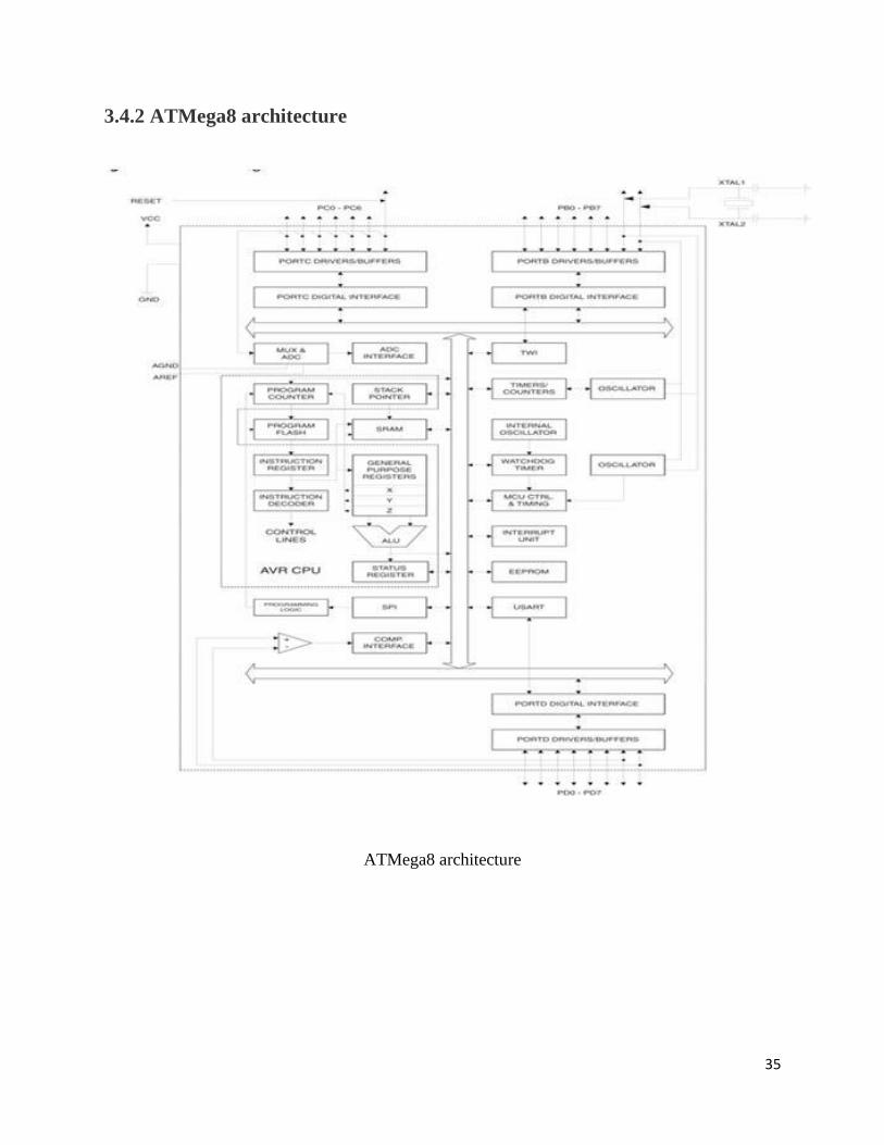
3.4.2 ATMega8 architecture
ATMega8 architecture
36
Memory
It consists of 8KB of flash memory, 1KB of SRAM and 512 Bytes of EEPROM. The 8K flash is
divided into 2 parts- lower part used as boot flash section, and upper part used as application
flash section. The SRAM contains 1K bytes along with 1120 bytes of general purpose registers
and I/O registers. The lower 32 address locations are used for 32 general purpose 8 bit registers.
The next 64 address are used for I/O registers. All the registers are connected directly to the
ALU. The EEPROM is used to store user defined data.
Input/output ports
It consists of 23 I/O lines with 3 I/O ports, named B, C and D. Port B consists of 8 I/O lines, Port
C consists of 7 I/O lines and Port D consists of 8 I/O lines.
Registers corresponding to any port X (B,C or D) are:
DDRX: Port X data direction register
PORTX: Port X data register
PINX: Port X input register
Timers and Counters
It consists of 3 timers with comparable modes. Two of them are 8 bit whereas the third one is 16
bit.
Oscillators
It incorporates internal reset and oscillator which makes it possible to eliminate the need for any
external input. The internal RC oscillator is capable of generating internal clock which can run at
any frequency of 1MHz, 2MHz, 4MHz or 8MHz as programmed. It also supports external
oscillator with maximum frequency of 16MHz.
37
Communication
It provides both synchronous and asynchronous data transfer schemes through USART
(Universal Synchronous and Asynchronous Receiver Transmitter), i.e. communication with
modems and other serial devices. It also supports SPI(Serial Peripheral Interface) used for
communication between devices based on the master-slave method. Another type of
communication supported is the TWI(Two wire Interface).
It allows commutation between any two devices by using 2 wires along with a common ground
connection.
It also has a comparator module integrated in the chip to provide comparison between two
voltages connected to the two inputs of the Analog comparator through the external chips.
It also contains a 6 channel ADC out of which 4 have 10 bit accuracy and 2 have 8 bit accuracy.
Status Register: It contains information about the currently executed arithmetic instruction set.
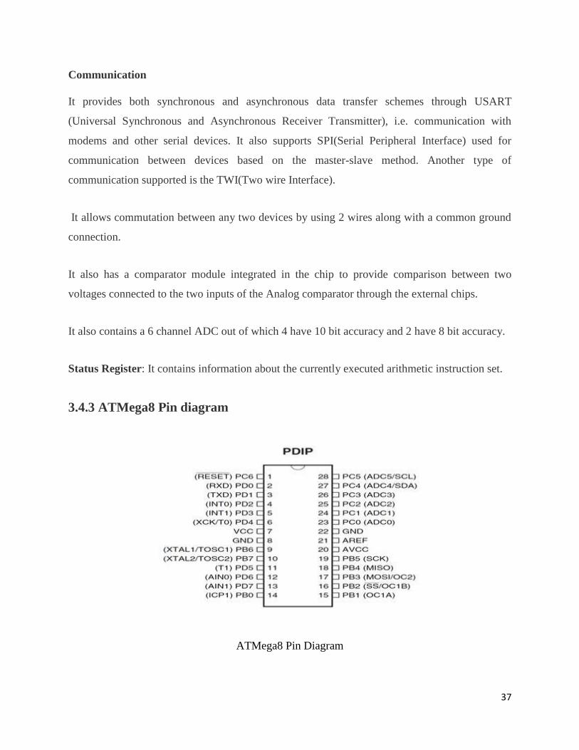
3.4.3 ATMega8 Pin diagram
ATMega8 Pin Diagram
38
Pins 23,24,25,26,27,28 and 1 are used for port C, whereas pins 9,10,14,15,16,17,18,19 are
used for port B and pins 2,3,4,5,6,11,12 are used for port D.
Pin 1 is also the Reset pin and applying low level signal for a time longer than the minimum
pulse length will generate a reset.
Pins 2 and 3 are also used for serial communication for USART.
Pins 4 and 5 are used as external interrupts. One of them will trigger when interrupt flag bit of
status register is set and the other will trigger as long as the interrupt condition prevails.
Pins 9 and 10 are used as external oscillator as well as timer counters oscillators where the
crystal is connected directly between the pins. Pin 10 is used for crystal oscillator or low
frequency crystal oscillator. If the internal calibrated RC oscillator is used as the clock source
and the asynchronous timer is enabled, these pins can be used as a timer oscillator pins.
Pin 19 is used as Master Clock output, slave clock input for SPI channel.
Pin 18 is used as Master clock input, slave clock output.
Pin 17 is used as Master data output, slave data input for SPI channel. It is used as a input
when enabled by a slave and is bidirectional when enabled by the master. This pin can also be
used as a output compare match output, which serves as an external output for the
timer/counter compare match.
Pin16 is used as a slave select input. It can also be used as a timer/counter1 compare match by
configuring the PB2 pin as an output.
39
Pin15 can be used as an external output for the timer/counter compare match A.
Pins 23 to 28 are used for ADC channels. Pin 27 can also be used as Serial interface clock and
pin 28 can be used as serial interface data
Pins 13 and 12 are used as Analog Comparator inputs.
Pins 11 and 6 are used as timer/counter sources.
3.4.4 ATMega8 sleep modes
The Microcontroller operates in 6 sleep modes.
Idle Mode: It stops the functioning of the CPU, but allows operation of SPI, USART, ADC,
TWI, Timer/Counter, and Watchdog and interrupts system. It is achieved by setting SM0 to
SM2 bits of MCU register flag to zero.
ADC Noise Reduction Mode: It stops the CPU but allows functioning of ADC, external
interrupts, timer/counter2 and watchdog.
Power down Mode: It enables external interrupts, the 2-wire serial interface, watchdog while
disabling the external oscillator. It stops all generated clocks.
Power save Mode: It is used when Timer/Counter is clocked asynchronously. It halts all
clocks except clkASY.
Stand By mode: In this mode, the oscillator is allowed to operate, halting all other
operations.
40
3.5 Summary
AVR microcontrollers are RISC based controllers, manufactured by Atmel group. They consist
of built is features like timers, analog to digital converters etc. Different AVR microcontrollers
are ATMega8, ATMega32, and ATMega328 etc. ATMega8 is a 28 pin microcontroller with
8KB of program memory and 1536 bytes of data memory. ATMega32 is a 40 pin
microcontroller with 32 programmable input/output lines. ATMega328 is a 28 pin
microcontroller with program memory of 32KB and data memory of 3KB.
41
Chapter 4- PIC Microcontrollers
4.1 Introduction
4.1.1 Brief idea about PIC microcontrollers
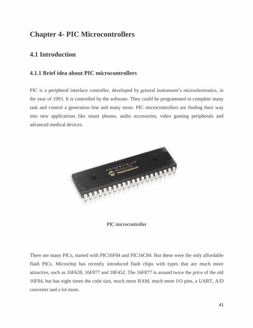
PIC is a peripheral interface controller, developed by general instrument’s microelectronics, in
the year of 1993. It is controlled by the software. They could be programmed to complete many
task and control a generation line and many more. PIC microcontrollers are finding their way
into new applications like smart phones, audio accessories, video gaming peripherals and
advanced medical devices.
PIC microcontroller
There are many PICs, started with PIC16F84 and PIC16C84. But these were the only affordable
flash PICs. Microchip has recently introduced flash chips with types that are much more
attractive, such as 16F628, 16F877 and 18F452. The 16F877 is around twice the price of the old
16F84, but has eight times the code size, much more RAM, much more I/O pins, a UART, A/D
converter and a lot more.
42
4.1.2 Key Features about PIC microcontrollers
Core Features:
High-performance RISC CPU
Up to 8K x 14 words of FLASH program memory
35 Instructions (fixed length encoding-14-bit)
368×8 static RAM based data memory
Up to 256 x 8 bytes of EEPROM data memory
Interrupt capability (up to 14 sources)
Three addressing modes (direct, indirect, relative)
Power-on reset (POR)
Harvard architecture memory
Power saving SLEEP mode
Wide operating voltage range: 2.0V to 5.5V
High sink / source current: 25mA
Accumulator based machine
Peripheral Features
3 Timer/counters (programmable pre-scalars): Timer0, Timer2 are 8-bit timer/counter with 8-
bit pre-scalar. Timer1 is 16-bit, can be incremented during sleep via external crystal/clock
Two capture, compare, PWM modules: Input capture function records the Timer1 count on a
pin transition. A PWM function output is a square wave with a programmable period and duty
cycle.
10-bit 8 channel analog-to-digital converter
43
USART with 9-bit address detection
Synchronous serial port with master mode and I2C Master/Slave
8-bit parallel slave port
Analog Features:
10-bit, up to 8-channel Analog-to-Digital Converter (A/D)
Brown-out Reset (BOR)
Analog Comparator module (Programmable input multiplexing from device inputs and
comparator outputs are externally accessible).
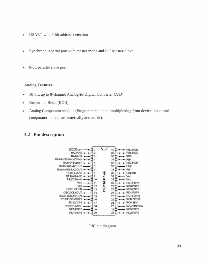
4.2 Pin description
PIC pin diagram
46
4.3 PIC Microcontroller architecture
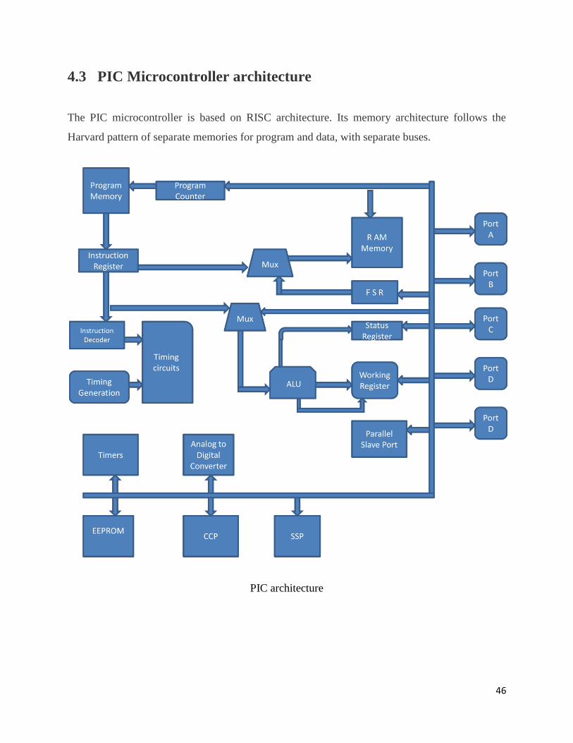
The PIC microcontroller is based on RISC architecture. Its memory architecture follows the
Harvard pattern of separate memories for program and data, with separate buses.
PIC architecture
47
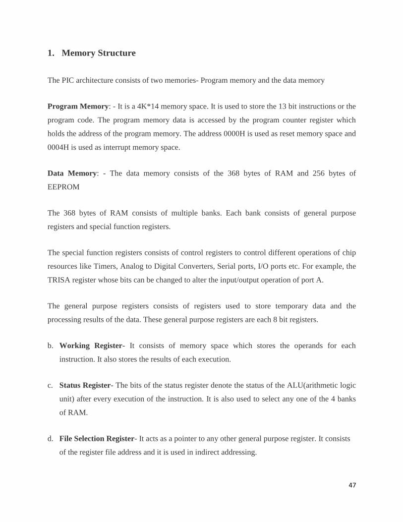
1. Memory Structure
The PIC architecture consists of two memories- Program memory and the data memory
Program Memory: - It is a 4K*14 memory space. It is used to store the 13 bit instructions or the
program code. The program memory data is accessed by the program counter register which
holds the address of the program memory. The address 0000H is used as reset memory space and
0004H is used as interrupt memory space.
Data Memory: - The data memory consists of the 368 bytes of RAM and 256 bytes of
EEPROM
The 368 bytes of RAM consists of multiple banks. Each bank consists of general purpose
registers and special function registers.
The special function registers consists of control registers to control different operations of chip
resources like Timers, Analog to Digital Converters, Serial ports, I/O ports etc. For example, the
TRISA register whose bits can be changed to alter the input/output operation of port A.
The general purpose registers consists of registers used to store temporary data and the
processing results of the data. These general purpose registers are each 8 bit registers.
b. Working Register- It consists of memory space which stores the operands for each
instruction. It also stores the results of each execution.
c. Status Register- The bits of the status register denote the status of the ALU(arithmetic logic
unit) after every execution of the instruction. It is also used to select any one of the 4 banks
of RAM.
d. File Selection Register- It acts as a pointer to any other general purpose register. It consists
of the register file address and it is used in indirect addressing.
48
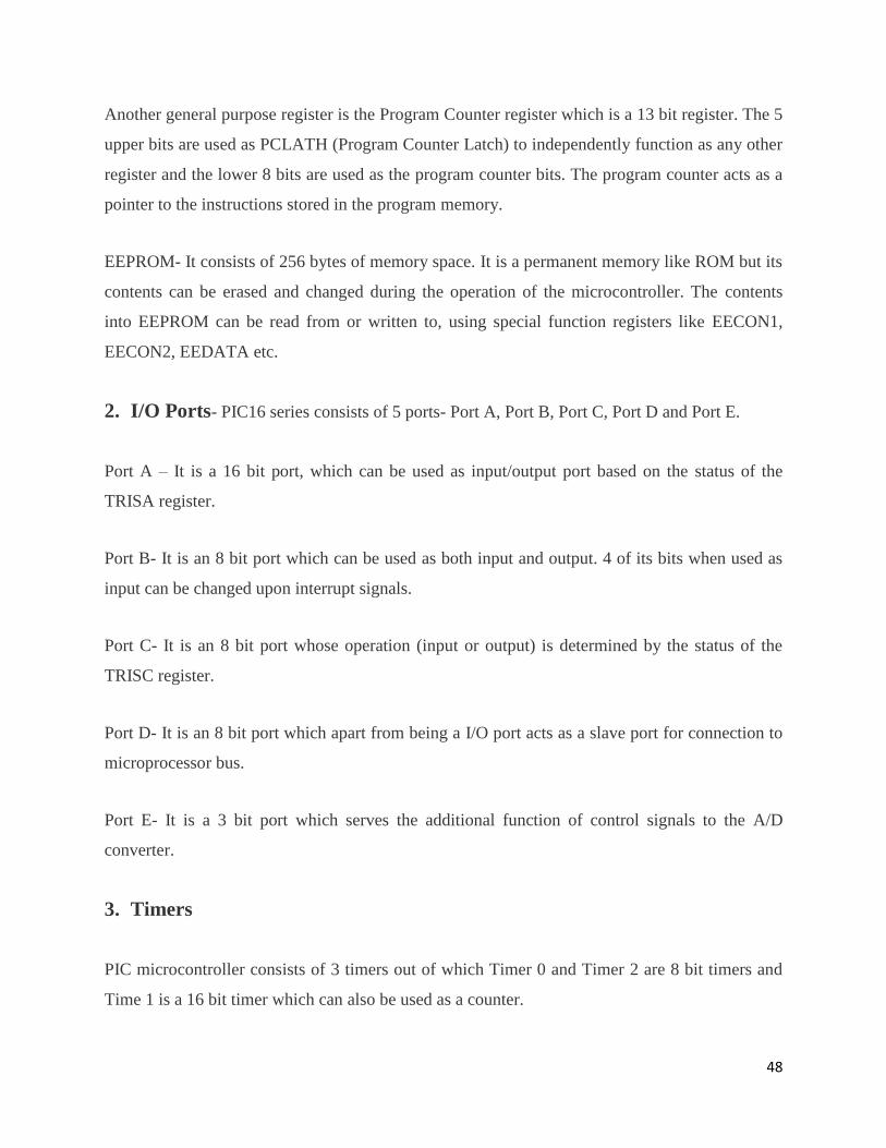
Another general purpose register is the Program Counter register which is a 13 bit register. The 5
upper bits are used as PCLATH (Program Counter Latch) to independently function as any other
register and the lower 8 bits are used as the program counter bits. The program counter acts as a
pointer to the instructions stored in the program memory.
EEPROM- It consists of 256 bytes of memory space. It is a permanent memory like ROM but its
contents can be erased and changed during the operation of the microcontroller. The contents
into EEPROM can be read from or written to, using special function registers like EECON1,
EECON2, EEDATA etc.
2. I/O Ports- PIC16 series consists of 5 ports- Port A, Port B, Port C, Port D and Port E.
Port A – It is a 16 bit port, which can be used as input/output port based on the status of the
TRISA register.
Port B- It is an 8 bit port which can be used as both input and output. 4 of its bits when used as
input can be changed upon interrupt signals.
Port C- It is an 8 bit port whose operation (input or output) is determined by the status of the
TRISC register.
Port D- It is an 8 bit port which apart from being a I/O port acts as a slave port for connection to
microprocessor bus.
Port E- It is a 3 bit port which serves the additional function of control signals to the A/D
converter.
3. Timers
PIC microcontroller consists of 3 timers out of which Timer 0 and Timer 2 are 8 bit timers and
Time 1 is a 16 bit timer which can also be used as a counter.
49
4. A/D Converter
The PIC Microcontroller consists of 8 channels, 10 bit Analog to Digital Converter. The
operation of A/D converter is controlled by the special function registers- ADCON0 and
ADCON1. The lower bits of the converter are stored in ADRESL (8 bits) and upper bits are
stored in ADRESH register. It requires an analog reference voltage of 5V for its operation.
5. Oscillators
Oscillators are used for timing generation. PIC microcontroller consists of external oscillators
like crystals or RC oscillators. In case of crystal oscillators, the crystal is connected between two
oscillator pins and the value of capacitor connected to each pin determines the mode of operation
of the oscillator. The different modes are low power mode, crystal mode and the high speed
mode. In case of RC oscillators, value of Resistor and Capacitor determine the clock frequency.
The clock frequency ranges from 30 KHz to 4 MHz
6. CCP module- A CCP module works in three modes-
Capture Mode- Captures the time of arrival of a signal or in other words captures the value of
Timer1 when CCP pin goes high.
Compare Mode- It acts as an analog comparator which generates an output when timer1 value
reaches a certain reference value.
PWM Mode: - It provides pulse width modulated output with 10 bit resolution and
programmable duty cycle.
7. Other special peripherals are like- Watchdog timer which resets the microcontroller incase of
any software malfunction, Brown out reset, which resets the microcontroller incase of any
power fluctuation and many more.
50
4.4 Summary
PIC or peripheral inter phase microcontrollers are Harvard architecture based microcontrollers
and consist of RISC based processor. A PIC microcontroller consists of additional peripherals
like analog to digital converter, PWM module, timers etc. A PIC microcontroller has a fixed
instruction set of 35 instructions.
51
Chapter 5-ARM Microcontrollers
5.1 Introduction
5.1.1 History
ARM stands for Advanced RISC (reduced instruction set computer) machine. ARM started as
part of Acorn makers of the BCC computer, and now designs chip for apple iPad. The first ARM
was established in Cambridge University in 1978. The Acorn group computers have developed
the first ARM commercial RISC processor in 1985. ARM was founded and became very popular
in 1990.
5.1.2 ARM usage
The ARM using more than 98% of the mobile phones in 2007 and 10 billion processors are
shipped in 2008. ARM is the latest technology which replaced by microcontroller and
microprocessors. Basically ARM is a 16 bit/ 32 bit Processors or Controllers. ARM is heart of
the advanced digital products like mobile phones automotive systems digital cameras and home
networking and wireless technologies.
5.1.3 ARM different versions and key features
52
Version 1:
Software interrupts
26-bit address bus
Data processing is slow
It support byte, word and multiword load operations
Version 2:
26-Bit address bus
Automatic instructions for thread synchronization
Co-processor support
Version 3:
32-Bit addressing
Multiple data support (like 32 bit=32*32=64).
Faster than ARM version1 and version2
Version 4:
32-bit address space
Its support T variant:16 bit THUMB instruction set
It support M variant: long multiply means give a 64 bit result
53
Version 5:
Improved ARM THUMB interworking
Its supports CCL instructions
It support E variant : Enhanced DSP Instruction set
It support S variant : Acceleration of Java byte code execution
Version 6:
Improved memory system
Its supports a single instruction multiple data
5.2 ARM architecture
ARM is based on reducing instruction set computer architecture; it means the core cannot
directly operate with the memory. All data operations must be done by registers with the
information which is located in the memory. Performing the operation of data and storing the
value back to the memory. ARM consists of 37 register sets, 31 general purpose registers and 6
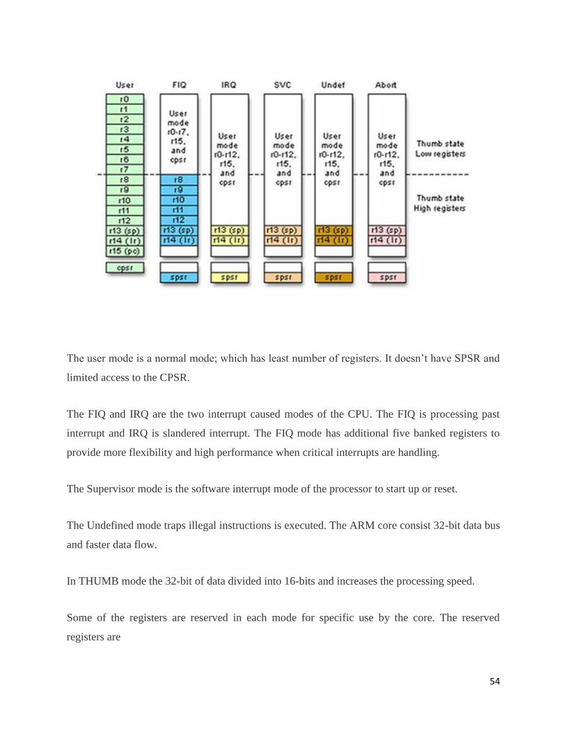
are status registers. The ARM uses seven processing modes that are used to run the user task.
USER mode
FIQ mode
IRQ mode
SVC mode
UNDEFINED mode
ABORT mode
THUMB mode
54
The user mode is a normal mode; which has least number of registers. It doesn’t have SPSR and
limited access to the CPSR.
The FIQ and IRQ are the two interrupt caused modes of the CPU. The FIQ is processing past
interrupt and IRQ is slandered interrupt. The FIQ mode has additional five banked registers to
provide more flexibility and high performance when critical interrupts are handling.
The Supervisor mode is the software interrupt mode of the processor to start up or reset.
The Undefined mode traps illegal instructions is executed. The ARM core consist 32-bit data bus
and faster data flow.
In THUMB mode the 32-bit of data divided into 16-bits and increases the processing speed.
Some of the registers are reserved in each mode for specific use by the core. The reserved
registers are
55
SP (stack pointer).
LR (link register).
PC (program counter).
CPSR (current program status register).
SPSR (saved program status register).
The reserved registers are used for specific functions. The SPSR and CPSR contain the status
control bits specific properties. These properties are defining operating mode, ALU status flag,
Interrupt enable or disable flags. The ARM core is operated in two states - 32-bit state or
THUMBS state.
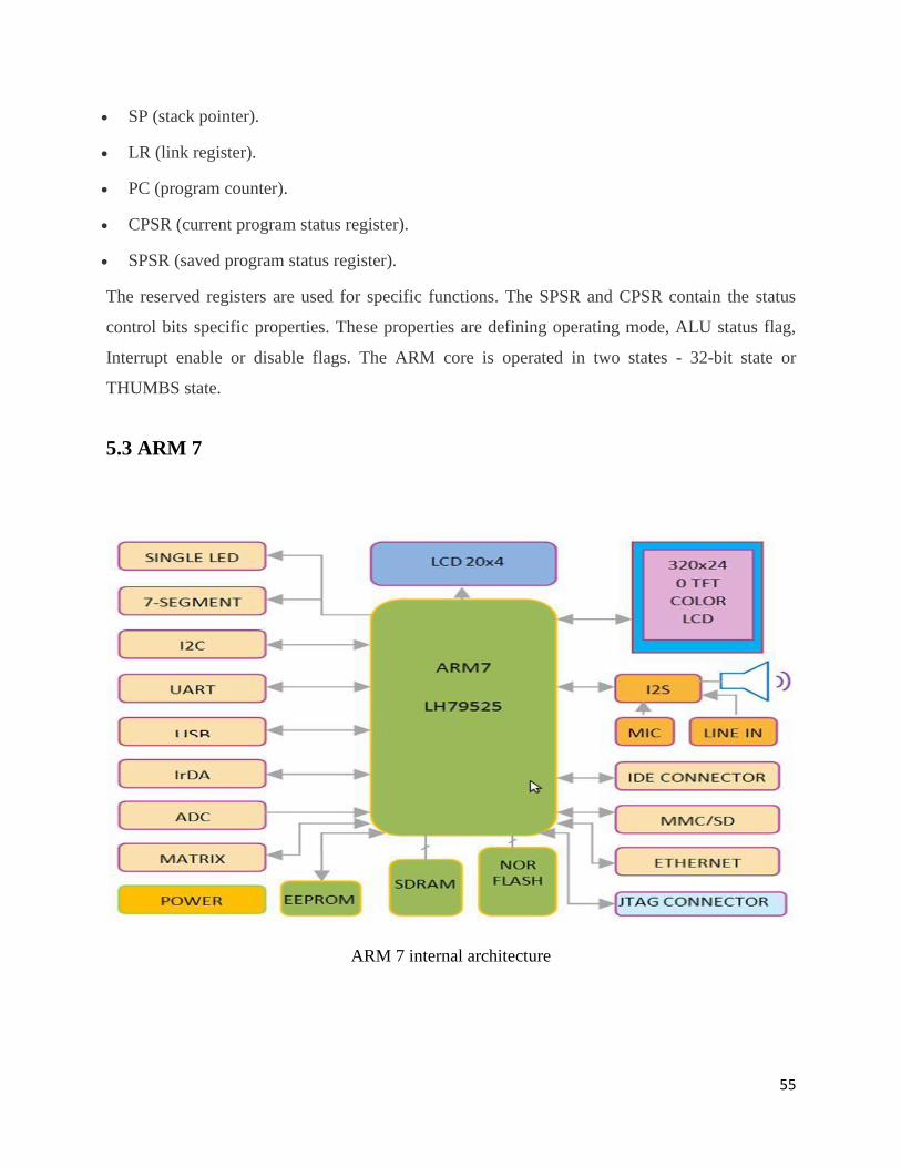
5.3 ARM 7
ARM 7 internal architecture
56
The ARM7 is a 16/31 – Bit bus
The static Ram is 40 kb
On-chip flash programmable memory is 512kb
It is a high speed controller 60 MHz operation
Two 10 bit ADC converters provide a total of 14 analog inputs
One 10- bit D/A converter
Two 32 bit timers/counters
4- CCM (Capture Compare Modulation), 6-PWM, Watchdog timer
One RTC, 9 interrupts
One I2C protocol, SPI protocols, SSP protocol
Two UART serial communication protocols
5.4 Summary
ARM microcontrollers are based on advance RISC based processors. They are 32 bit
microcontrollers. They can be operated in two modes-thumb mode and normal mode. ARM
microcontroller families are ARM7, ARM9 and Cortex.
57
Chapter 6- Renesas Microcontrollers
6.1 Introduction to Renesas Microcontrollers
Renesas is the latest automotive microcontroller family that offers high performance feature with
exceptionally low power consumption over a wide and versatile extension of items. This
microcontroller offers rich functional security and embedded safety characteristics required for
new and advanced automotive applications. The core structure of microcontroller CPU supports
high reliability and high performance requirements.
The RX Family of 32-bit microcontrollers is a feature rich, general purpose MCU covering a
wide range of embedded control applications with high speed connectivity, digital signal
processing and inverter control.
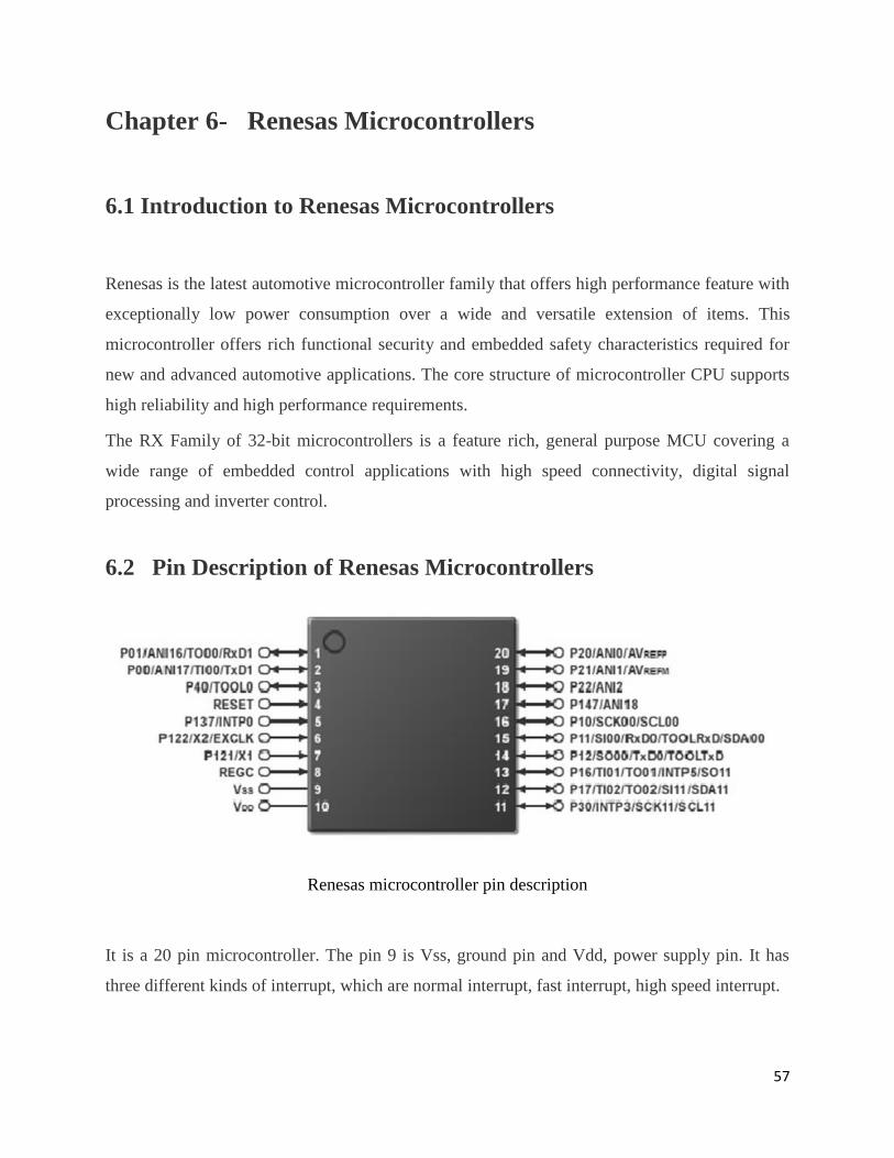
6.2 Pin Description of Renesas Microcontrollers
Renesas microcontroller pin description
It is a 20 pin microcontroller. The pin 9 is Vss, ground pin and Vdd, power supply pin. It has
three different kinds of interrupt, which are normal interrupt, fast interrupt, high speed interrupt.
58
Normal interrupts store the significant registers on stack by using push and pop instructions. The
fast interrupts are automatically store program counter and processor status word in special
backup registers, so response time is faster. And high speed interrupts allocate up to four of the
general registers for dedicated use by the interrupt to expand speed even further. The internal bus
structure gives 5 internal busses to ensure data handling is not slowed down. Instruction fetches
occur via a wide 64-bit bus, so that due to the variable length instructions used in CISC
architectures.
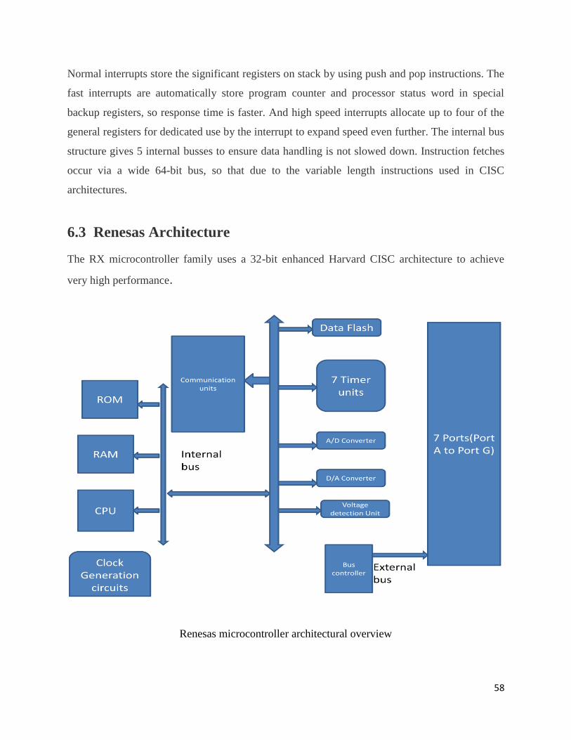
6.3 Renesas Architecture
The RX microcontroller family uses a 32-bit enhanced Harvard CISC architecture to achieve
very high performance.
Renesas microcontroller architectural overview
59
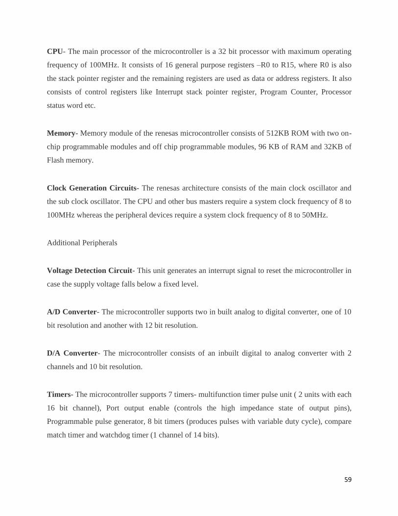
CPU- The main processor of the microcontroller is a 32 bit processor with maximum operating
frequency of 100MHz. It consists of 16 general purpose registers –R0 to R15, where R0 is also
the stack pointer register and the remaining registers are used as data or address registers. It also
consists of control registers like Interrupt stack pointer register, Program Counter, Processor
status word etc.
Memory- Memory module of the renesas microcontroller consists of 512KB ROM with two on-
chip programmable modules and off chip programmable modules, 96 KB of RAM and 32KB of
Flash memory.
Clock Generation Circuits- The renesas architecture consists of the main clock oscillator and
the sub clock oscillator. The CPU and other bus masters require a system clock frequency of 8 to
100MHz whereas the peripheral devices require a system clock frequency of 8 to 50MHz.
Additional Peripherals
Voltage Detection Circuit- This unit generates an interrupt signal to reset the microcontroller in
case the supply voltage falls below a fixed level.
A/D Converter- The microcontroller supports two in built analog to digital converter, one of 10
bit resolution and another with 12 bit resolution.
D/A Converter- The microcontroller consists of an inbuilt digital to analog converter with 2
channels and 10 bit resolution.
Timers- The microcontroller supports 7 timers- multifunction timer pulse unit ( 2 units with each
16 bit channel), Port output enable (controls the high impedance state of output pins),
Programmable pulse generator, 8 bit timers (produces pulses with variable duty cycle), compare
match timer and watchdog timer (1 channel of 14 bits).
60
Communication devices- The microcontroller provides several peripherals for communication
like Ethernet Controller ( 10 to 100Mbps data rate), USB 2.0 host (12Mbps data rate), Serial
communication units like smart card interface, CAN(control area network) unit , serial peripheral
interface units.
6.4 Summary
Renesas microcontrollers are 32 bit microcontrollers based on Harvard architecture, with
variable instruction set. They consist of additional features like analog to digital converter,
digital to analog converter, watch dog timers etc. It consists of 512KB of flash Ethernet.
61
Chapter 7- Microcontroller Communication
7.1 Introduction
By microcontroller communication, we refer to communication between two microcontrollers or
communication between a microcontroller and other devices. There a set of rules known as
protocols to govern this communication. The communication between a microcontroller and
devices on same chip/circuit is the intra system communication whereas the communication
between a microcontroller and devices on other chips/circuits is inters system communication.
7.2 Inter System Protocol
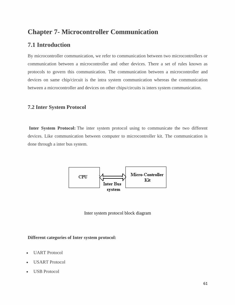
Inter System Protocol: The inter system protocol using to communicate the two different
devices. Like communication between computer to microcontroller kit. The communication is
done through a inter bus system.
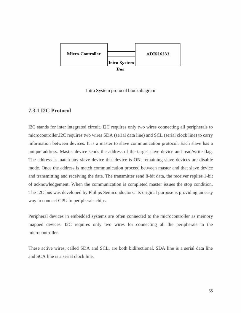
Inter system protocol block diagram
Different categories of Inter system protocol:
UART Protocol
USART Protocol
USB Protocol
62
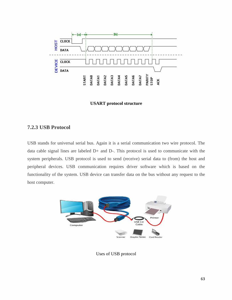
7.2.1 UART Protocol
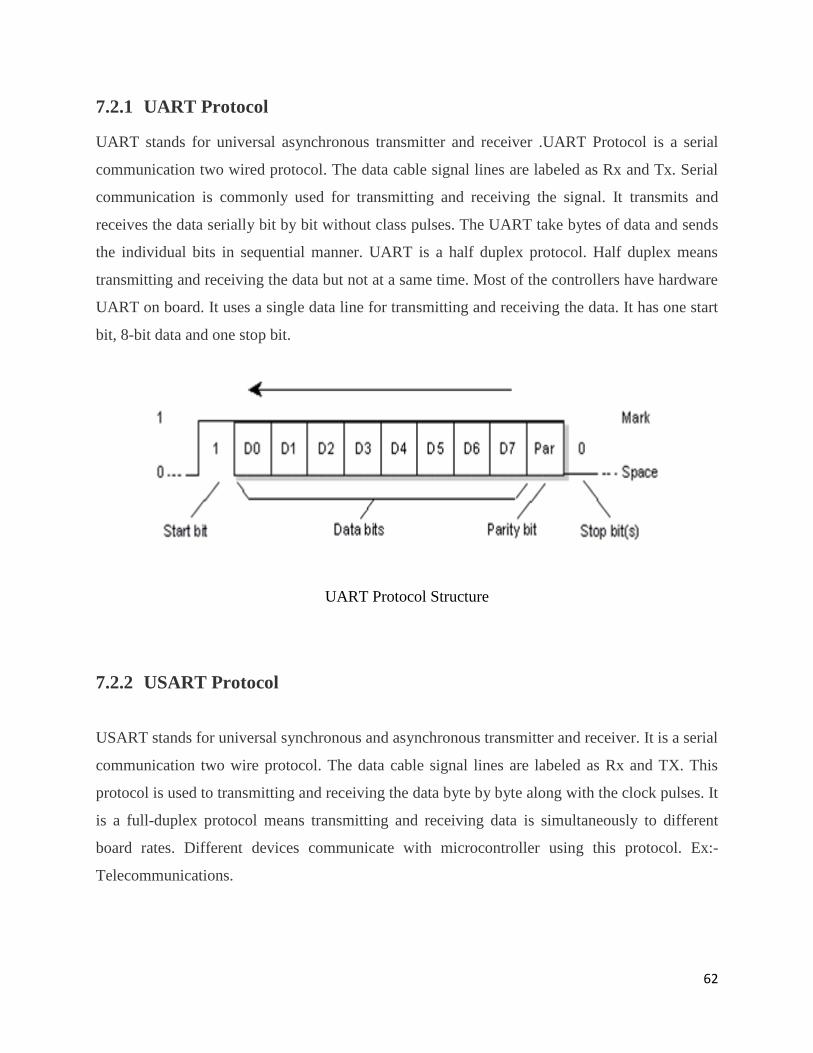
UART stands for universal asynchronous transmitter and receiver .UART Protocol is a serial
communication two wired protocol. The data cable signal lines are labeled as Rx and Tx. Serial
communication is commonly used for transmitting and receiving the signal. It transmits and
receives the data serially bit by bit without class pulses. The UART take bytes of data and sends
the individual bits in sequential manner. UART is a half duplex protocol. Half duplex means
transmitting and receiving the data but not at a same time. Most of the controllers have hardware
UART on board. It uses a single data line for transmitting and receiving the data. It has one start
bit, 8-bit data and one stop bit.
UART Protocol Structure
7.2.2 USART Protocol
USART stands for universal synchronous and asynchronous transmitter and receiver. It is a serial
communication two wire protocol. The data cable signal lines are labeled as Rx and TX. This
protocol is used to transmitting and receiving the data byte by byte along with the clock pulses. It
is a full-duplex protocol means transmitting and receiving data is simultaneously to different
board rates. Different devices communicate with microcontroller using this protocol. Ex:-
Telecommunications.
63
USART protocol structure
7.2.3 USB Protocol
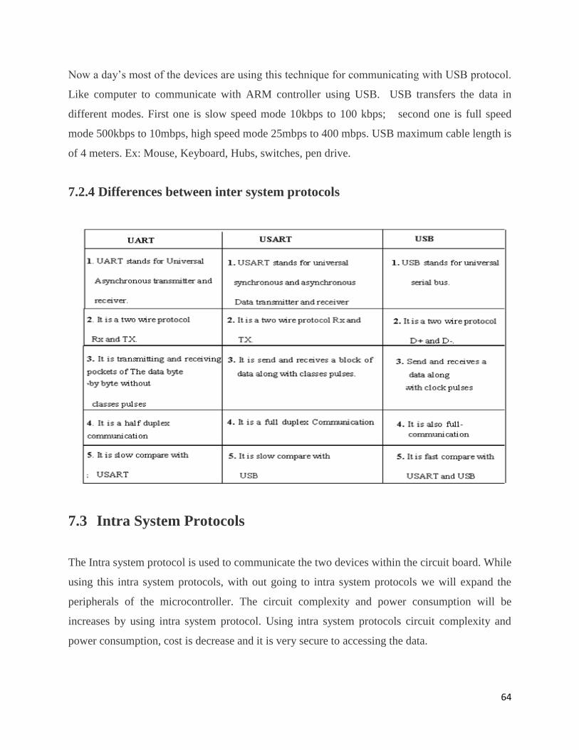
USB stands for universal serial bus. Again it is a serial communication two wire protocol. The
data cable signal lines are labeled D+ and D-. This protocol is used to communicate with the
system peripherals. USB protocol is used to send (receive) serial data to (from) the host and
peripheral devices. USB communication requires driver software which is based on the
functionality of the system. USB device can transfer data on the bus without any request to the
host computer.
Uses of USB protocol
64
Now a day’s most of the devices are using this technique for communicating with USB protocol.
Like computer to communicate with ARM controller using USB. USB transfers the data in
different modes. First one is slow speed mode 10kbps to 100 kbps; second one is full speed
mode 500kbps to 10mbps, high speed mode 25mbps to 400 mbps. USB maximum cable length is
of 4 meters. Ex: Mouse, Keyboard, Hubs, switches, pen drive.
7.2.4 Differences between inter system protocols
7.3 Intra System Protocols
The Intra system protocol is used to communicate the two devices within the circuit board. While
using this intra system protocols, with out going to intra system protocols we will expand the
peripherals of the microcontroller. The circuit complexity and power consumption will be
increases by using intra system protocol. Using intra system protocols circuit complexity and
power consumption, cost is decrease and it is very secure to accessing the data.
65
Intra System protocol block diagram
7.3.1 I2C Protocol
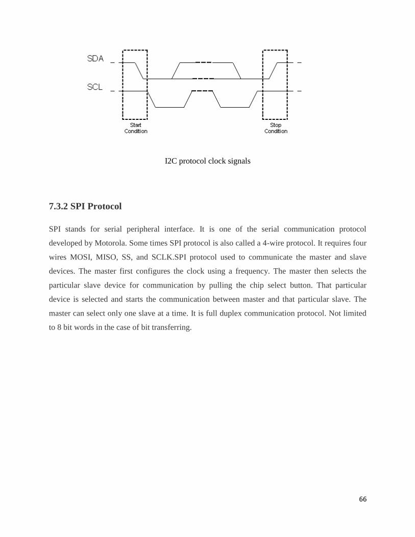
I2C stands for inter integrated circuit. I2C requires only two wires connecting all peripherals to
microcontroller.I2C requires two wires SDA (serial data line) and SCL (serial clock line) to carry
information between devices. It is a master to slave communication protocol. Each slave has a
unique address. Master device sends the address of the target slave device and read/write flag.
The address is match any slave device that device is ON, remaining slave devices are disable
mode. Once the address is match communication proceed between master and that slave device
and transmitting and receiving the data. The transmitter send 8-bit data, the receiver replies 1-bit
of acknowledgement. When the communication is completed master issues the stop condition.
The I2C bus was developed by Philips Semiconductors. Its original purpose is providing an easy
way to connect CPU to peripherals chips.
Peripheral devices in embedded systems are often connected to the microcontroller as memory
mapped devices. I2C requires only two wires for connecting all the peripherals to the
microcontroller.
These active wires, called SDA and SCL, are both bidirectional. SDA line is a serial data line
and SCA line is a serial clock line.
66
I2C protocol clock signals
7.3.2 SPI Protocol
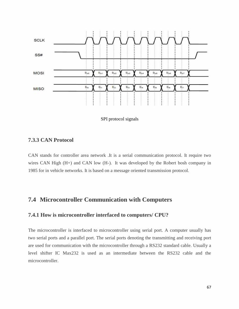
SPI stands for serial peripheral interface. It is one of the serial communication protocol
developed by Motorola. Some times SPI protocol is also called a 4-wire protocol. It requires four
wires MOSI, MISO, SS, and SCLK.SPI protocol used to communicate the master and slave
devices. The master first configures the clock using a frequency. The master then selects the
particular slave device for communication by pulling the chip select button. That particular
device is selected and starts the communication between master and that particular slave. The
master can select only one slave at a time. It is full duplex communication protocol. Not limited
to 8 bit words in the case of bit transferring.
67
SPI protocol signals
7.3.3 CAN Protocol
CAN stands for controller area network .It is a serial communication protocol. It require two
wires CAN High (H+) and CAN low (H-). It was developed by the Robert bosh company in
1985 for in vehicle networks. It is based on a message oriented transmission protocol.
7.4 Microcontroller Communication with Computers
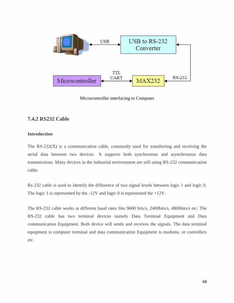
7.4.1 How is microcontroller interfaced to computers/ CPU?
The microcontroller is interfaced to microcontroller using serial port. A computer usually has
two serial ports and a parallel port. The serial ports denoting the transmitting and receiving port
are used for communication with the microcontroller through a RS232 standard cable. Usually a
level shifter IC Max232 is used as an intermediate between the RS232 cable and the
microcontroller.
68
Microcontroller interfacing to Computer
7.4.2 RS232 Cable
Introduction
The RS-232(X) is a communication cable, commonly used for transferring and receiving the
serial data between two devices. It supports both synchronous and asynchronous data
transmissions. Many devices in the industrial environment are still using RS-232 communication
cable.
Rs-232 cable is used to identify the difference of two signal levels between logic 1 and logic 0.
The logic 1 is represented by the -12V and logic 0 is represented the +12V.
The RS-232 cable works at different baud rates like 9600 bits/s, 2400bits/s, 4800bits/s etc. The
RS-232 cable has two terminal devices namely Data Terminal Equipment and Data
communication Equipment. Both device will sends and receives the signals. The data terminal
equipment is computer terminal and data communication Equipment is modems, or controllers
etc.
69
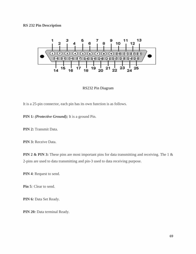
RS 232 Pin Description
RS232 Pin Diagram
It is a 25-pin connector, each pin has its own function is as follows.
PIN 1: (Protective Ground); It is a ground Pin.
PIN 2: Transmit Data.
PIN 3: Receive Data.
PIN 2 & PIN 3: These pins are most important pins for data transmitting and receiving. The 1 &
2-pins are used to data transmitting and pin-3 used to data receiving purpose.
PIN 4: Request to send.
Pin 5: Clear to send.
PIN 6: Data Set Ready.
PIN 20: Data terminal Ready.
70
PIN 4, PIN 5, PIN 6, PIN 20: These pins are the handshaking pins(flow of control).Normally
terminals cannot transmit the data until clear to send transmission is received from the DCE.
PIN 7: This pin is the common reference for all signals, including data, timing, and control
signals. The DCE and DTE works properly across the serial interface and the pin-7 must be
connected both ends without interface would not work.
PIN 8: This pin also known as received line signal detect or carrier detect. This signal is
activated when a suitable carrier is established between the local and remote DCE devices.
PIN9: This pin is DTE serial connector; this signal follows the incoming ring to an extent.
Normally this signal is used by DCE auto answer mode.
PIN 10: Test Pin.
PIN 11: stand by select.
PIN 12: Data Carrier Detect.
PIN 13: Clear to send.
PIN 14: Transmit data.
PIN 15: Transmit clock.
PIN 17: Receive clock.
PIN 24: External Clock.
PIN 15, 17, 24; Synchronous modems use the signals on these pins. These pins are control bit
timing.
71
PIN 16: Receive data.
PIN 18: Test Pin.
PIN 19: Request to send.
PIN 21: (Signal Quality Detector); This pin Indicates the quality of the received carrier signal
because the transmitting modem must be send 0 or either 1 at each bit time , the modem controls
the timing of the bits from the DTE.
PIN 22: (Ring Indicator): The ringing indicator means the DCE informs the DTE that the phone
is ringing. All the modems designed for direct connected to the phone network equipped with
auto answer.
PIN 23: Data Signal Rate Detector
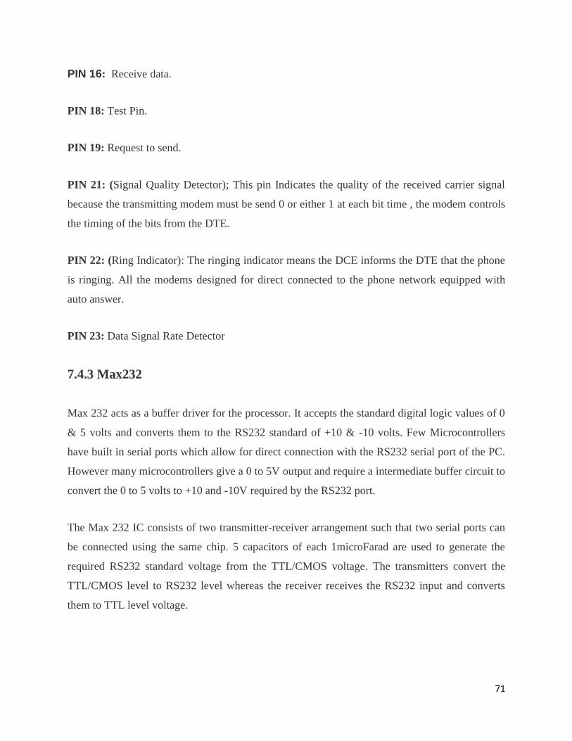
7.4.3 Max232
Max 232 acts as a buffer driver for the processor. It accepts the standard digital logic values of 0
& 5 volts and converts them to the RS232 standard of +10 & -10 volts. Few Microcontrollers
have built in serial ports which allow for direct connection with the RS232 serial port of the PC.
However many microcontrollers give a 0 to 5V output and require a intermediate buffer circuit to
convert the 0 to 5 volts to +10 and -10V required by the RS232 port.
The Max 232 IC consists of two transmitter-receiver arrangement such that two serial ports can
be connected using the same chip. 5 capacitors of each 1microFarad are used to generate the
required RS232 standard voltage from the TTL/CMOS voltage. The transmitters convert the
TTL/CMOS level to RS232 level whereas the receiver receives the RS232 input and converts
them to TTL level voltage.
72
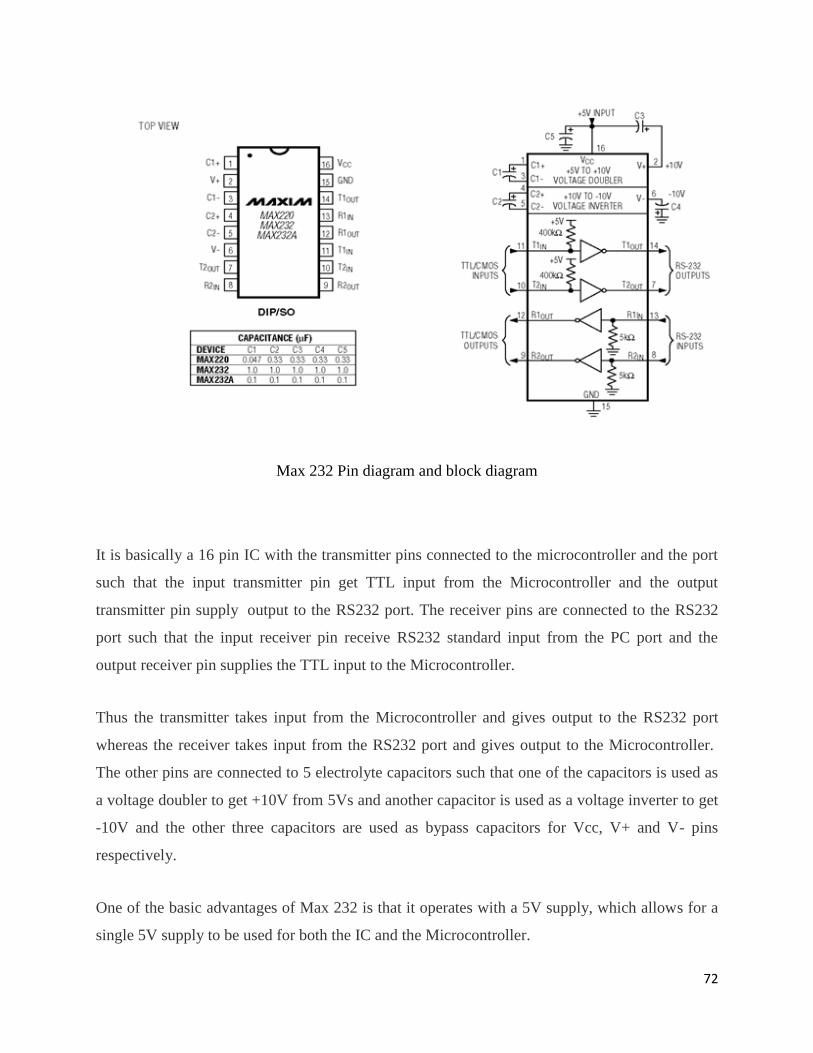
Max 232 Pin diagram and block diagram
It is basically a 16 pin IC with the transmitter pins connected to the microcontroller and the port
such that the input transmitter pin get TTL input from the Microcontroller and the output
transmitter pin supply output to the RS232 port. The receiver pins are connected to the RS232
port such that the input receiver pin receive RS232 standard input from the PC port and the
output receiver pin supplies the TTL input to the Microcontroller.
Thus the transmitter takes input from the Microcontroller and gives output to the RS232 port
whereas the receiver takes input from the RS232 port and gives output to the Microcontroller.
The other pins are connected to 5 electrolyte capacitors such that one of the capacitors is used as
a voltage doubler to get +10V from 5Vs and another capacitor is used as a voltage inverter to get
-10V and the other three capacitors are used as bypass capacitors for Vcc, V+ and V- pins
respectively.
One of the basic advantages of Max 232 is that it operates with a 5V supply, which allows for a
single 5V supply to be used for both the IC and the Microcontroller.
73
7.5 Summary
A microcontroller can communicate with devices on the same circuit board or devices on other
circuit board. When communicating with devices on the same circuit board, the communication
protocols used are called intra system protocols, example being I2C protocol. When
communicating with devices on different circuit board, the communication protocols used are
called inter system protocols, example being USB protocol. For a microcontroller to
communicate with a computer, R2C standard cables are used which is interfaced using Max232
level shifter IC.
74
Chapter 8-Programming the Microcontroller
8.1 Introduction to programming a microcontroller
By the term programming a microcontroller, we refer to the set of instructions written and stored
in the microcontroller to carry out a particular task. These instructions or program can be written
using Assembly level language or C language.
8.2 Assembly Level Language Programming
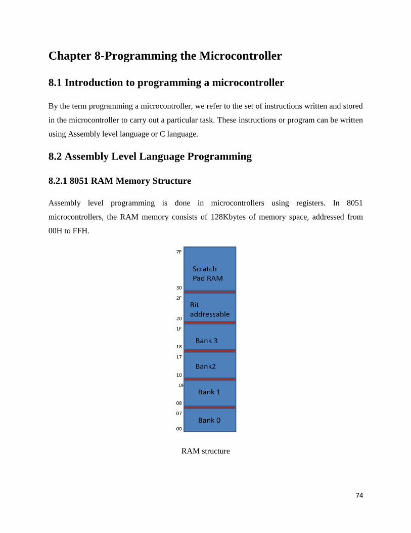
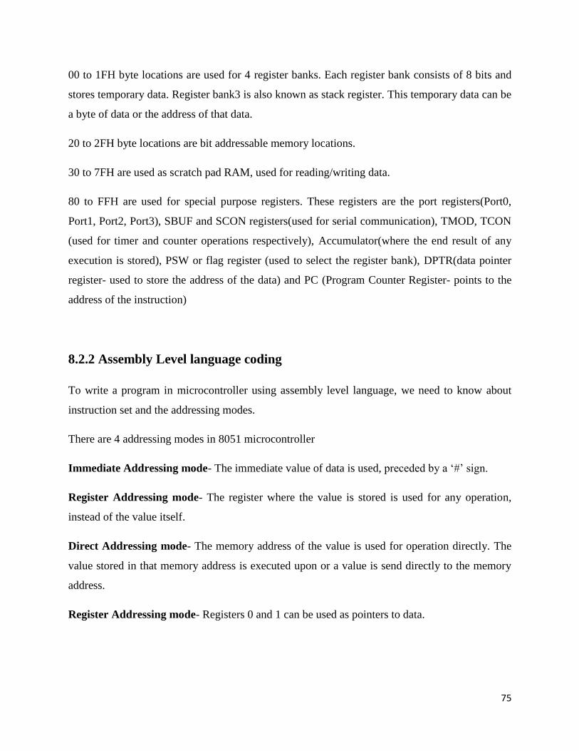
8.2.1 8051 RAM Memory Structure
Assembly level programming is done in microcontrollers using registers. In 8051
microcontrollers, the RAM memory consists of 128Kbytes of memory space, addressed from
00H to FFH.
RAM structure
75
00 to 1FH byte locations are used for 4 register banks. Each register bank consists of 8 bits and
stores temporary data. Register bank3 is also known as stack register. This temporary data can be
a byte of data or the address of that data.
20 to 2FH byte locations are bit addressable memory locations.
30 to 7FH are used as scratch pad RAM, used for reading/writing data.
80 to FFH are used for special purpose registers. These registers are the port registers(Port0,
Port1, Port2, Port3), SBUF and SCON registers(used for serial communication), TMOD, TCON
(used for timer and counter operations respectively), Accumulator(where the end result of any
execution is stored), PSW or flag register (used to select the register bank), DPTR(data pointer
register- used to store the address of the data) and PC (Program Counter Register- points to the
address of the instruction)
8.2.2 Assembly Level language coding
To write a program in microcontroller using assembly level language, we need to know about
instruction set and the addressing modes.
There are 4 addressing modes in 8051 microcontroller
Immediate Addressing mode- The immediate value of data is used, preceded by a ‘#’ sign.
Register Addressing mode- The register where the value is stored is used for any operation,
instead of the value itself.
Direct Addressing mode- The memory address of the value is used for operation directly. The
value stored in that memory address is executed upon or a value is send directly to the memory
address.
Register Addressing mode- Registers 0 and 1 can be used as pointers to data.
76
An assembly level program consists of the following parts-
Label: - Defines a name or label for that particular instruction.
Directives- Directs any operation involving the operands. Examples are ORG, EQU, and END
etc
Mnemonics- Define the particular operation to be carried out. They are converted to Opcodes,
which are codes defining the instructions
Operands- Denote the values or registers upon which operation is carried out.
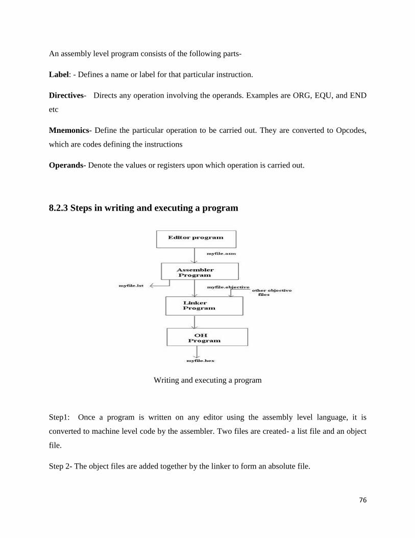
8.2.3 Steps in writing and executing a program
Writing and executing a program
Step1: Once a program is written on any editor using the assembly level language, it is
converted to machine level code by the assembler. Two files are created- a list file and an object
file.
Step 2- The object files are added together by the linker to form an absolute file.
77
Step 3- This absolute file is then converted to hex file using object to hex converter.
Step 4- This hex file is burned into the ROM of the microcontroller. The ROM contains the
opcodes for each instruction.
Step 5- Once the microcontroller is powered up, it starts with 0000 location of ROM.
Step 6 - The instructions are executed one by one and program counter gets incremented
accordingly.
8.3 C Language Programming
Today, we can use many different programming languages such as C, JAVA, ORACLE and
others. These languages are called high level languages; to write the program in high level
language the programmer doesn’t need any knowledge on hardware which is used for high level
application development. The compiler plays a vital role in translating the high-level program to
machine level as the high level languages are used in native development.
8.3.1 Software used in microcontroller programming
The most popular software tool used for microcontroller programming is Kiel software. This
software is an integrated development environment (IDE) which is integrated with a text editor
to write programs, a compiler to convert the high level language to machine language.
78
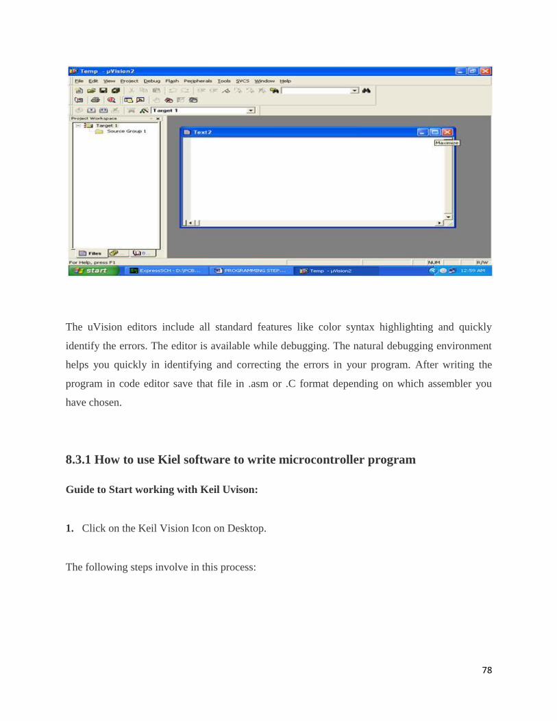
The uVision editors include all standard features like color syntax highlighting and quickly
identify the errors. The editor is available while debugging. The natural debugging environment
helps you quickly in identifying and correcting the errors in your program. After writing the
program in code editor save that file in .asm or .C format depending on which assembler you
have chosen.
8.3.1 How to use Kiel software to write microcontroller program
Guide to Start working with Keil Uvison:
1. Click on the Keil Vision Icon on Desktop.
The following steps involve in this process:
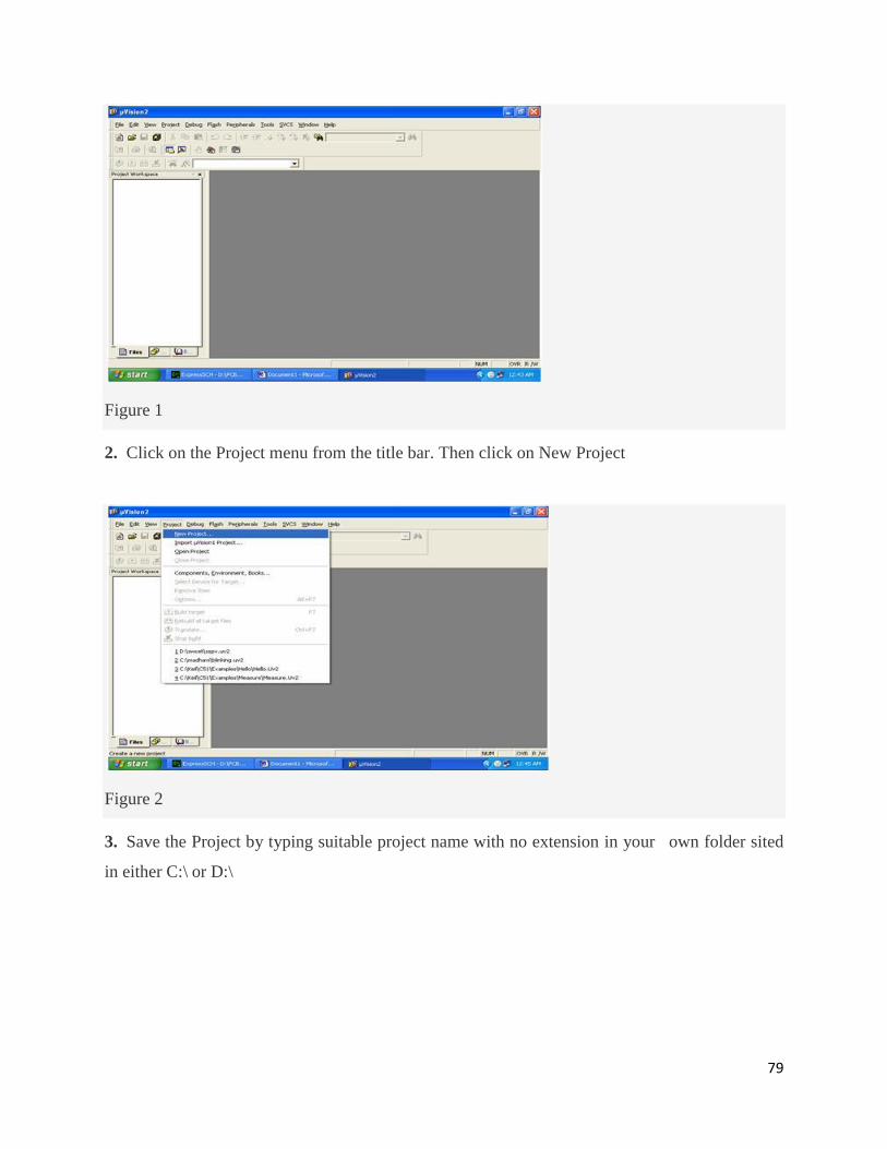
79
Figure 1
2. Click on the Project menu from the title bar. Then click on New Project
Figure 2
3. Save the Project by typing suitable project name with no extension in your own folder sited
in either C:\ or D:\
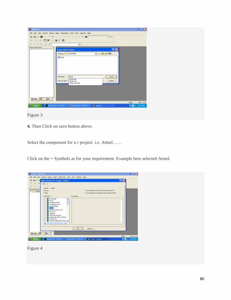
80
Figure 3
4. Then Click on save button above.
Select the component for u r project. i.e. Atmel……
Click on the + Symbols as for your requirement. Example here selected Atmel.
Figure 4
81
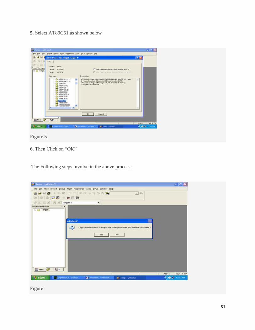
5. Select AT89C51 as shown below
Figure 5
6. Then Click on “OK”
The Following steps involve in the above process:
Figure
82
7. Then Click either YES or NO………mostly “NO”.
Now your project is ready to USE.
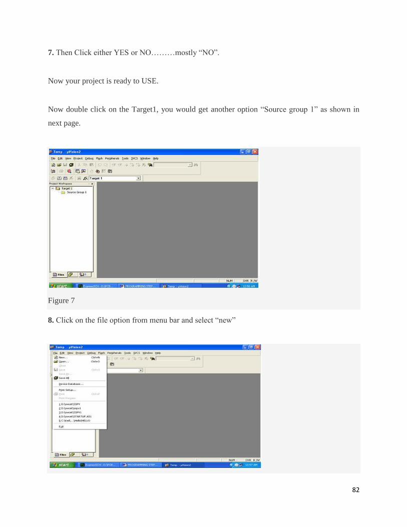
Now double click on the Target1, you would get another option “Source group 1” as shown in
next page.
Figure 7
8. Click on the file option from menu bar and select “new”
83
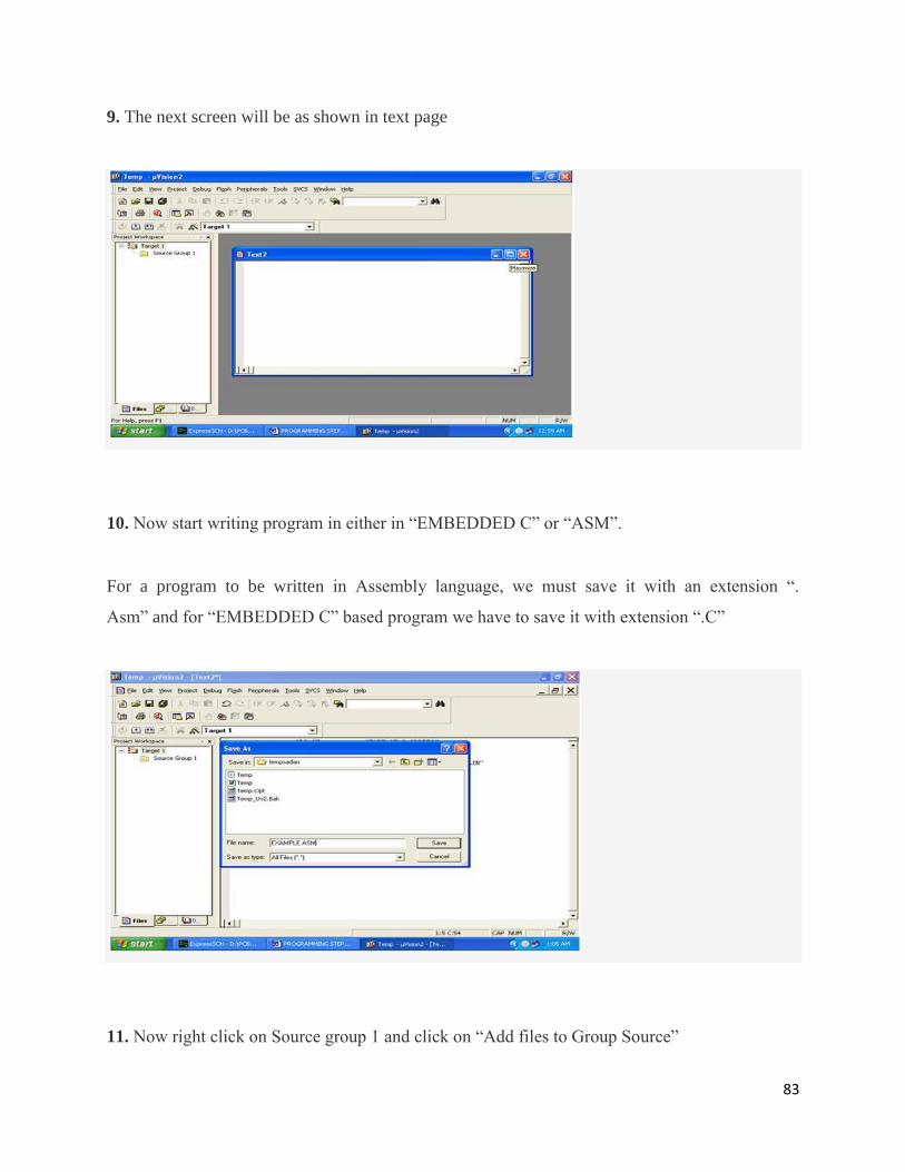
9. The next screen will be as shown in text page
10. Now start writing program in either in “EMBEDDED C” or “ASM”.
For a program to be written in Assembly language, we must save it with an extension “.
Asm” and for “EMBEDDED C” based program we have to save it with extension “.C”
11. Now right click on Source group 1 and click on “Add files to Group Source”
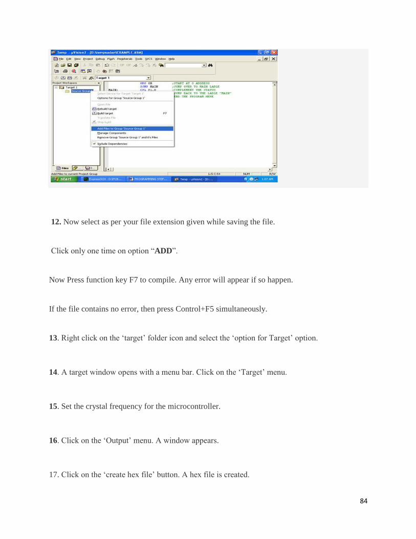
84
12. Now select as per your file extension given while saving the file.
Click only one time on option “ADD”.
Now Press function key F7 to compile. Any error will appear if so happen.
If the file contains no error, then press Control+F5 simultaneously.
13. Right click on the ‘target’ folder icon and select the ‘option for Target’ option.
14. A target window opens with a menu bar. Click on the ‘Target’ menu.
15. Set the crystal frequency for the microcontroller.
16. Click on the ‘Output’ menu. A window appears.
17. Click on the ‘create hex file’ button. A hex file is created.
85
8.3.3 Steps in developing a microcontroller program using C language.
1. The program is written on the editor using the above given steps.
2. The program in high level language is converted to machine level language by the compiler. It
involves the formation of the list file and the object files.
3. The object files are linked together by the linker program to form the absolute file.
4. This absolute file is then converted to hex file by the Object to Hex converter.
8.4 Summary
Microcontroller 8051 is the most popular used series of microcontrollers for any simple
embedded system. It can be programmed using Assembly language program or high level
language like C. Once a program is written, it is converted to machine language and burned into
microcontroller hardware using any burner software.
86
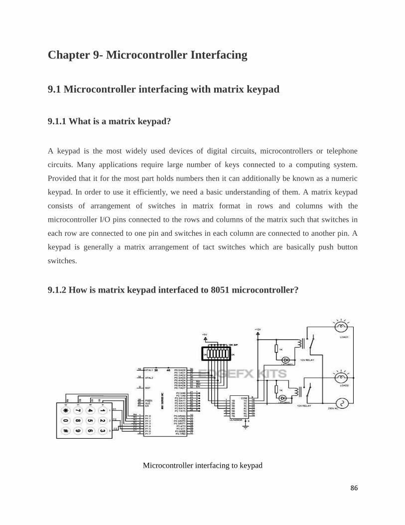
Chapter 9- Microcontroller Interfacing
9.1 Microcontroller interfacing with matrix keypad
9.1.1 What is a matrix keypad?
A keypad is the most widely used devices of digital circuits, microcontrollers or telephone
circuits. Many applications require large number of keys connected to a computing system.
Provided that it for the most part holds numbers then it can additionally be known as a numeric
keypad. In order to use it efficiently, we need a basic understanding of them. A matrix keypad
consists of arrangement of switches in matrix format in rows and columns with the
microcontroller I/O pins connected to the rows and columns of the matrix such that switches in
each row are connected to one pin and switches in each column are connected to another pin. A
keypad is generally a matrix arrangement of tact switches which are basically push button
switches.
9.1.2 How is matrix keypad interfaced to 8051 microcontroller?
Microcontroller interfacing to keypad
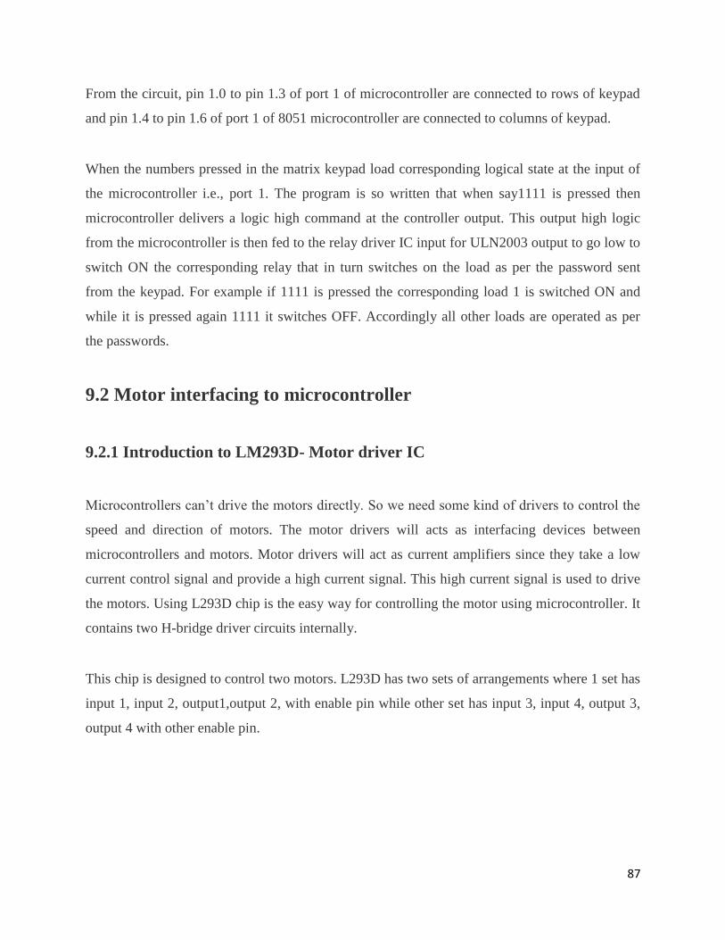
87
From the circuit, pin 1.0 to pin 1.3 of port 1 of microcontroller are connected to rows of keypad
and pin 1.4 to pin 1.6 of port 1 of 8051 microcontroller are connected to columns of keypad.
When the numbers pressed in the matrix keypad load corresponding logical state at the input of
the microcontroller i.e., port 1. The program is so written that when say1111 is pressed then
microcontroller delivers a logic high command at the controller output. This output high logic
from the microcontroller is then fed to the relay driver IC input for ULN2003 output to go low to
switch ON the corresponding relay that in turn switches on the load as per the password sent
from the keypad. For example if 1111 is pressed the corresponding load 1 is switched ON and
while it is pressed again 1111 it switches OFF. Accordingly all other loads are operated as per
the passwords.
9.2 Motor interfacing to microcontroller
9.2.1 Introduction to LM293D- Motor driver IC
Microcontrollers can’t drive the motors directly. So we need some kind of drivers to control the
speed and direction of motors. The motor drivers will acts as interfacing devices between
microcontrollers and motors. Motor drivers will act as current amplifiers since they take a low
current control signal and provide a high current signal. This high current signal is used to drive
the motors. Using L293D chip is the easy way for controlling the motor using microcontroller. It
contains two H-bridge driver circuits internally.
This chip is designed to control two motors. L293D has two sets of arrangements where 1 set has
input 1, input 2, output1,output 2, with enable pin while other set has input 3, input 4, output 3,
output 4 with other enable pin.
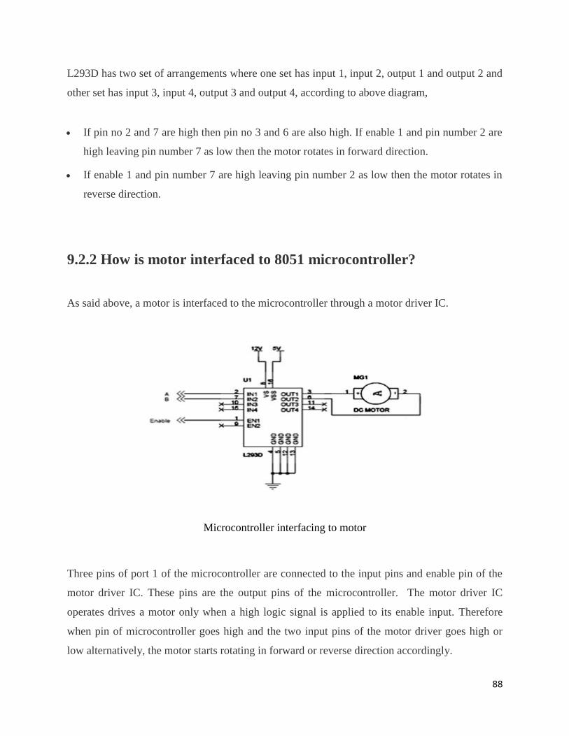
88
L293D has two set of arrangements where one set has input 1, input 2, output 1 and output 2 and
other set has input 3, input 4, output 3 and output 4, according to above diagram,
If pin no 2 and 7 are high then pin no 3 and 6 are also high. If enable 1 and pin number 2 are
high leaving pin number 7 as low then the motor rotates in forward direction.
If enable 1 and pin number 7 are high leaving pin number 2 as low then the motor rotates in
reverse direction.
9.2.2 How is motor interfaced to 8051 microcontroller?
As said above, a motor is interfaced to the microcontroller through a motor driver IC.
Microcontroller interfacing to motor
Three pins of port 1 of the microcontroller are connected to the input pins and enable pin of the
motor driver IC. These pins are the output pins of the microcontroller. The motor driver IC
operates drives a motor only when a high logic signal is applied to its enable input. Therefore
when pin of microcontroller goes high and the two input pins of the motor driver goes high or
low alternatively, the motor starts rotating in forward or reverse direction accordingly.
89
9.3 Relay interfacing to 8051 microcontroller
9.3.1 Introduction to Relay Drivers
A relay coil requires about 12V to be energized, whereas the output pin of the microcontroller is
at TTL logic level (about 5V). For this reason a driver is needed to act as an interface between
the microcontroller and the relay. This relay driver can be a MOSFET or a relay driver IC
ULN2003
9.3.2 Interfacing relay with microcontroller using relay driver IC ULN2003
A relay driver IC ULN2003 is a 16 pin IC. It is a high voltage IC consisting of 7 Darlington
pairs of transistors. It consists of 7 input pins and 7 corresponding output pins. In other words it
can drive 7 relays.
Microcontrollers interfacing with relay using ULN2003
90
Here pin of microcontroller is connected to input pin 1B of the microcontroller. When this input
goes high, i.e. a pulse is given to this pin; the output pin 1C of the driver goes low, i.e. connected
to ground. This output pin is connected to the relay such that current flows through the relay coil
and it gets energized.
9.3.3 Interfacing relay with microcontroller using transistor
A transistor can also be used as a relay driver. The basic idea is to use the switching operation of
the transistor.
One end of the relay coil is connected to 12V supply, whereas other end is connected to the
collector of the transistor. Base terminal of that transistor is connected to the output pin of the
microcontroller. When a pulse is applied to this pin, the transistor gets switched ON, the
collector and emitter terminals are shorted and get connected to ground. Current flows through
the relay coil and coil is energized.
9.4 16 by 2 LCD display interfacing to microcontroller
Many microcontroller devices are using smart LCD displays to output visual information. For an
8-bit data bus, the display requires a +5V supply plus 11 I/O lines. A 4 bit data bus requires
supply line as well as 7 extra lines. When the LCD display is not enabled, data lines are tri-state
which means they are in a state of high impedance and this means they do not interfere with the
microcontroller operation when display is not used.
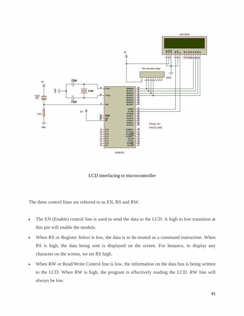
91
LCD interfacing to microcontroller
The three control lines are referred to as EN, RS and RW.
The EN (Enable) control line is used to send the data to the LCD. A high to low transition at
this pin will enable the module.
When RS or Register Select is low, the data is to be treated as a command instruction. When
RS is high, the data being sent is displayed on the screen. For Instance, to display any
character on the screen, we set RS high.
When RW or Read/Write Control line is low, the information on the data bus is being written
to the LCD. When RW is high, the program is effectively reading the LCD. RW line will
always be low.
92
The data bus consists of 4 or 8 lines; it depends on the mode of operation selected by the user.
The lines of an 8 bit data bus are referred to as DB0, DB1, DB2, DB3, DB4, DB5, DB6 and
DB7.
9.5 Summary
Microcontrollers can be interfaced to many devices like motors, relays, displays etc. Interfacing a
microcontroller with input or output devices is necessary for proper functioning of any
embedded system. Devices like motors, relays are interfaced using a driver IC, where as keypad
and displays are interfaced directly.
93
Chapter 10- Designing your own microcontroller based
projects
10.1 Step by step guide to build your own microcontroller based
projects
10.1.1 Introduction and theory about the project
I am sure there must be many of you, who would love to build your own embedded system or let
me say a simple project using a microcontroller. Now for this, you need to have a basic idea
about each step required to develop a microcontroller based project. So here I am explaining the
basic steps to build a microcontroller based project.
But before that, let us get an idea about the project we would like to design and the theory behind
it.
Aim of the project
To design a LED flash light system using Microcontroller
Theory
The LED flash light system can produce the light through light emitting diode. The incandescent
lights used in traditional flash light consume more energy and have very less life time. The LED
lights on the other hand, consume less energy and have long life.
Basic Idea behind the Design
The microcontroller generates the output logic pulses so that the LED light is switched ON and
OFF at certain intervals. It is a 40 pin microcontroller. The Crystal interfaced to input pins of the
microcontroller provide accurate clock signals at the crystal frequency.
94
10.1.2: Step1- Circuit Designing
The 8051 microcontroller crystal operates at 11.0592 MHz frequencies because it can give exact
clock pulses for data synchronizing. Two capacitors are connected to the crystal oscillator with
range of 20pf to 40pf which is used to stabilize the clock signals. The 8051 microcontroller at
some times goes to block state or missing time calculation.
At that time we need to reset the microcontroller. When the microcontroller is reset, it takes
maximum 3sec time delay with the help of the 10k resistor and 10uf capacitor.
Circuit Components:
Hardware Components:
Yellow LED
Crystal
Reset
8051 microcontroller
Capacitors
Resistors
Software Components:
Keil compiler
Proteus software
Embedded C language
Circuit Connections
The 5v DC supply is given to the 40 pin of the microcontroller which drives the circuit. The
crystal is connected to the 18 and 19 pin of the microcontroller.
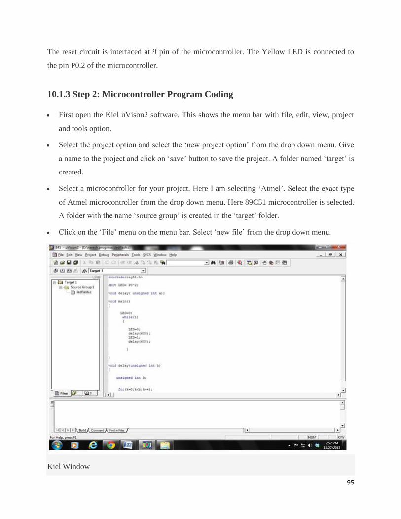
95
The reset circuit is interfaced at 9 pin of the microcontroller. The Yellow LED is connected to
the pin P0.2 of the microcontroller.
10.1.3 Step 2: Microcontroller Program Coding
First open the Kiel uVison2 software. This shows the menu bar with file, edit, view, project
and tools option.
Select the project option and select the ‘new project option’ from the drop down menu. Give
a name to the project and click on ‘save’ button to save the project. A folder named ‘target’ is
created.
Select a microcontroller for your project. Here I am selecting ‘Atmel’. Select the exact type
of Atmel microcontroller from the drop down menu. Here 89C51 microcontroller is selected.
A folder with the name ‘source group’ is created in the ‘target’ folder.
Click on the ‘File’ menu on the menu bar. Select ‘new file’ from the drop down menu.
Kiel Window
96
Write the code on the blank space.
The LED Flash Light program:
#include<reg51.h>
sbit LED= P0^2;
void delay( unsigned int a);
void main()
{ LED=0;
While (1)
{ LED=0;
delay(600);
LED=1;
delay(600);
}
}
void delay (unsigned int b)
{ unsigned int k;
97
for(k=0;k<b;k++);
}
Save this code with ‘.C’ extension.
Right click on the ‘source group’ folder icon and select ‘add files to group’ option.
A window appears. Select the ‘C’ file to be added.
Select the ‘debug’ menu. It checks the program for any errors.
Right click on the ‘target’ folder icon.
Select the ‘option for Target’ option.
A target window opens with a menu bar. Click on the ‘Target’ menu.
Set the crystal frequency for the microcontroller.
Click on the ‘Output’ menu. A window appears
Click on the ‘create hex file’ button. A hex file is created.
10.1.4: Step 3: Circuit Drawing
This is circuit is designed with help of Proteus software. It is circuit design software which
contains a database of components which we can use to build the circuit. Each and every
component is available in the components library.
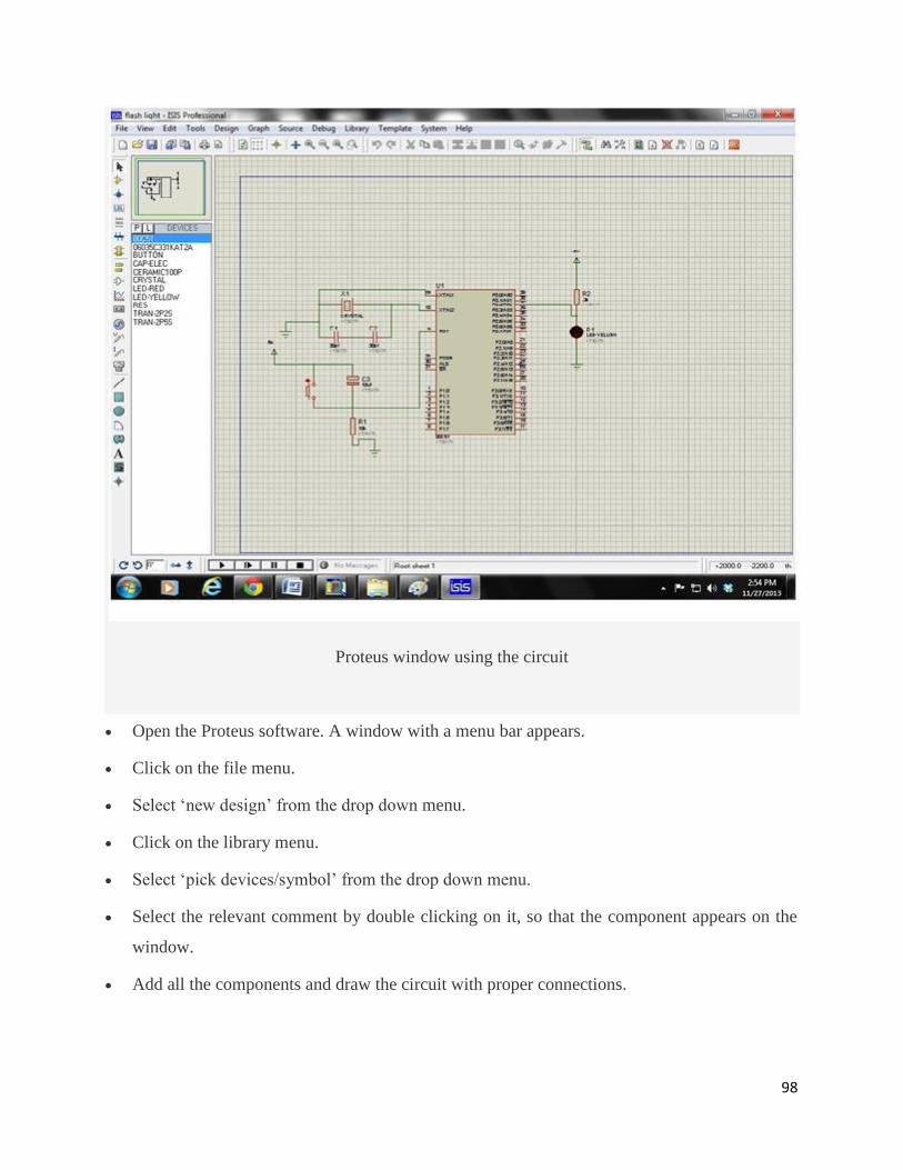
98
Proteus window using the circuit
Open the Proteus software. A window with a menu bar appears.
Click on the file menu.
Select ‘new design’ from the drop down menu.
Click on the library menu.
Select ‘pick devices/symbol’ from the drop down menu.
Select the relevant comment by double clicking on it, so that the component appears on the
window.
Add all the components and draw the circuit with proper connections.
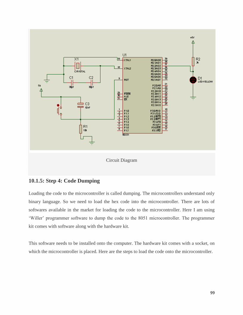
99
Circuit Diagram
10.1.5: Step 4: Code Dumping
Loading the code to the microcontroller is called dumping. The microcontrollers understand only
binary language. So we need to load the hex code into the microcontroller. There are lots of
softwares available in the market for loading the code to the microcontroller. Here I am using
‘Willer’ programmer software to dump the code to the 8051 microcontroller. The programmer
kit comes with software along with the hardware kit.
This software needs to be installed onto the computer. The hardware kit comes with a socket, on
which the microcontroller is placed. Here are the steps to load the code onto the microcontroller.
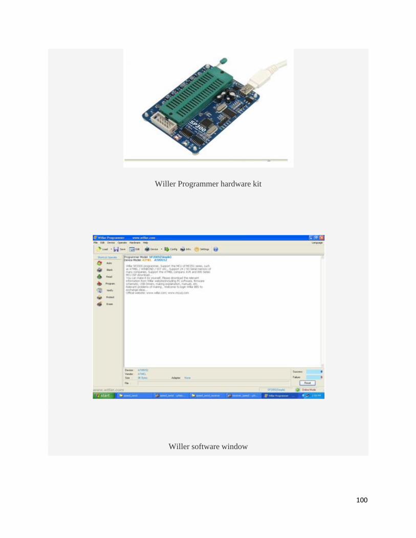
100
Willer Programmer hardware kit
Willer software window
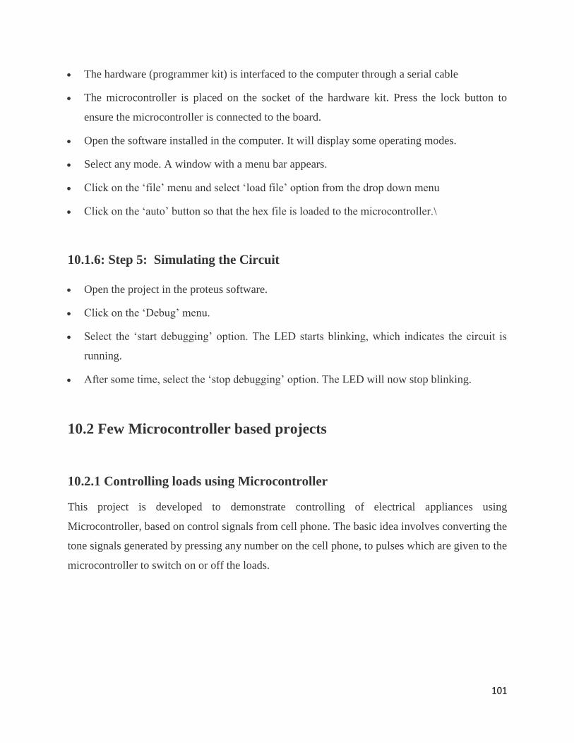
101
The hardware (programmer kit) is interfaced to the computer through a serial cable
The microcontroller is placed on the socket of the hardware kit. Press the lock button to
ensure the microcontroller is connected to the board.
Open the software installed in the computer. It will display some operating modes.
Select any mode. A window with a menu bar appears.
Click on the ‘file’ menu and select ‘load file’ option from the drop down menu
Click on the ‘auto’ button so that the hex file is loaded to the microcontroller.\
10.1.6: Step 5: Simulating the Circuit
Open the project in the proteus software.
Click on the ‘Debug’ menu.
Select the ‘start debugging’ option. The LED starts blinking, which indicates the circuit is
running.
After some time, select the ‘stop debugging’ option. The LED will now stop blinking.
10.2 Few Microcontroller based projects
10.2.1 Controlling loads using Microcontroller
This project is developed to demonstrate controlling of electrical appliances using
Microcontroller, based on control signals from cell phone. The basic idea involves converting the
tone signals generated by pressing any number on the cell phone, to pulses which are given to the
microcontroller to switch on or off the loads.
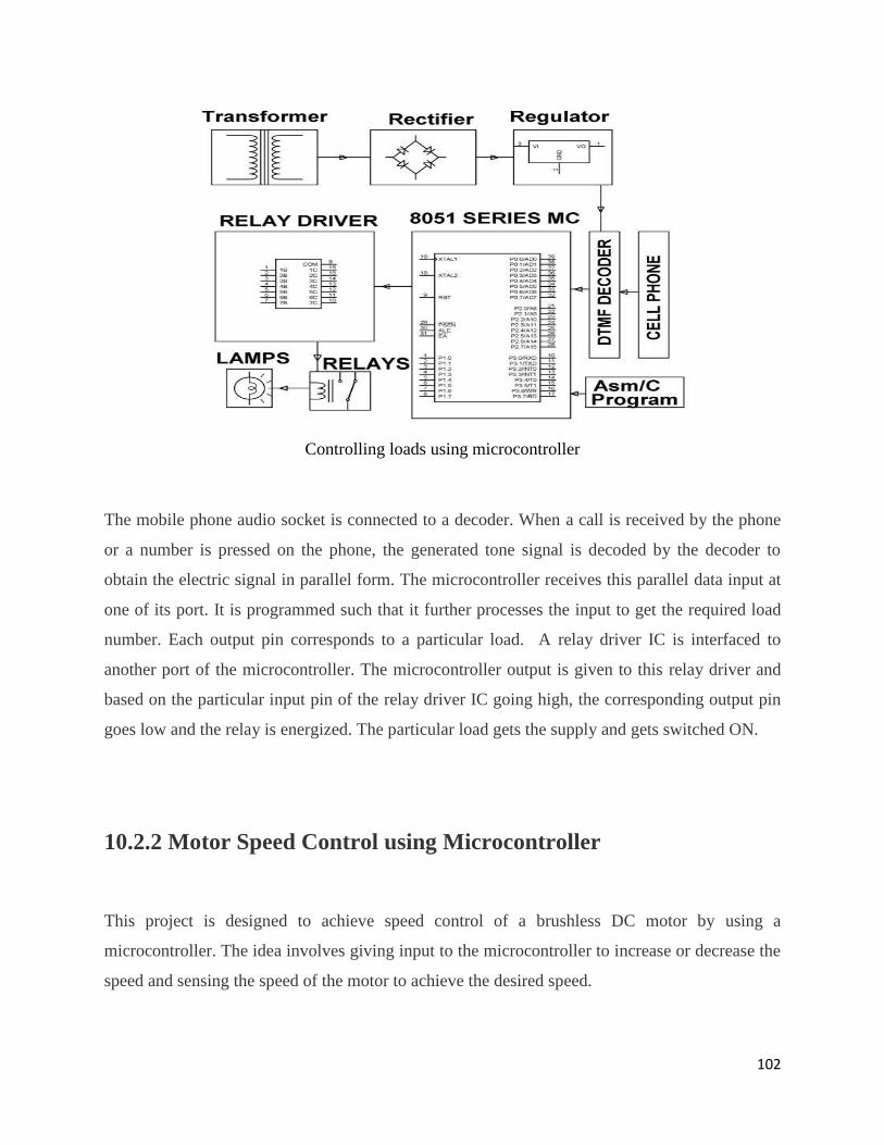
102
Controlling loads using microcontroller
The mobile phone audio socket is connected to a decoder. When a call is received by the phone
or a number is pressed on the phone, the generated tone signal is decoded by the decoder to
obtain the electric signal in parallel form. The microcontroller receives this parallel data input at
one of its port. It is programmed such that it further processes the input to get the required load
number. Each output pin corresponds to a particular load. A relay driver IC is interfaced to
another port of the microcontroller. The microcontroller output is given to this relay driver and
based on the particular input pin of the relay driver IC going high, the corresponding output pin
goes low and the relay is energized. The particular load gets the supply and gets switched ON.
10.2.2 Motor Speed Control using Microcontroller
This project is designed to achieve speed control of a brushless DC motor by using a
microcontroller. The idea involves giving input to the microcontroller to increase or decrease the
speed and sensing the speed of the motor to achieve the desired speed.
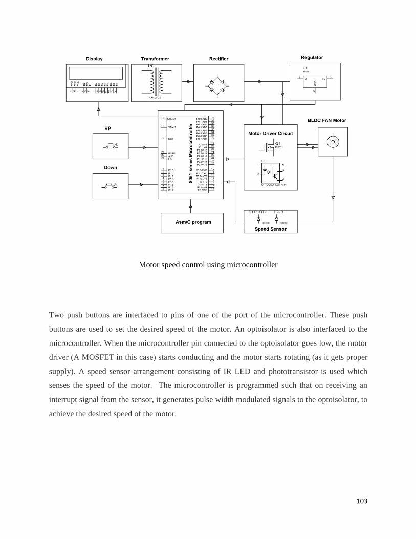
103
Motor speed control using microcontroller
Two push buttons are interfaced to pins of one of the port of the microcontroller. These push
buttons are used to set the desired speed of the motor. An optoisolator is also interfaced to the
microcontroller. When the microcontroller pin connected to the optoisolator goes low, the motor
driver (A MOSFET in this case) starts conducting and the motor starts rotating (as it gets proper
supply). A speed sensor arrangement consisting of IR LED and phototransistor is used which
senses the speed of the motor. The microcontroller is programmed such that on receiving an
interrupt signal from the sensor, it generates pulse width modulated signals to the optoisolator, to
achieve the desired speed of the motor.
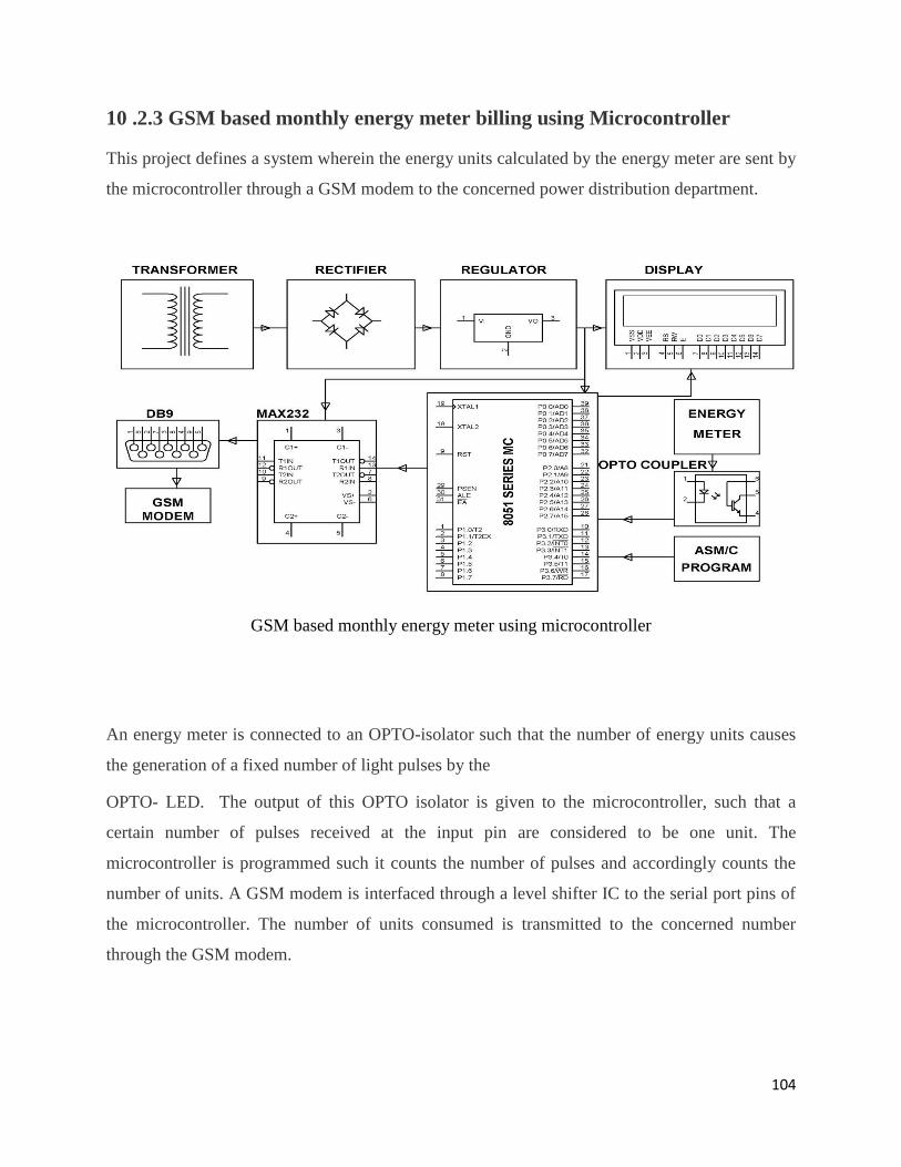
104
10 .2.3 GSM based monthly energy meter billing using Microcontroller
This project defines a system wherein the energy units calculated by the energy meter are sent by
the microcontroller through a GSM modem to the concerned power distribution department.
GSM based monthly energy meter using microcontroller
An energy meter is connected to an OPTO-isolator such that the number of energy units causes
the generation of a fixed number of light pulses by the
OPTO- LED. The output of this OPTO isolator is given to the microcontroller, such that a
certain number of pulses received at the input pin are considered to be one unit. The
microcontroller is programmed such it counts the number of pulses and accordingly counts the
number of units. A GSM modem is interfaced through a level shifter IC to the serial port pins of
the microcontroller. The number of units consumed is transmitted to the concerned number
through the GSM modem.
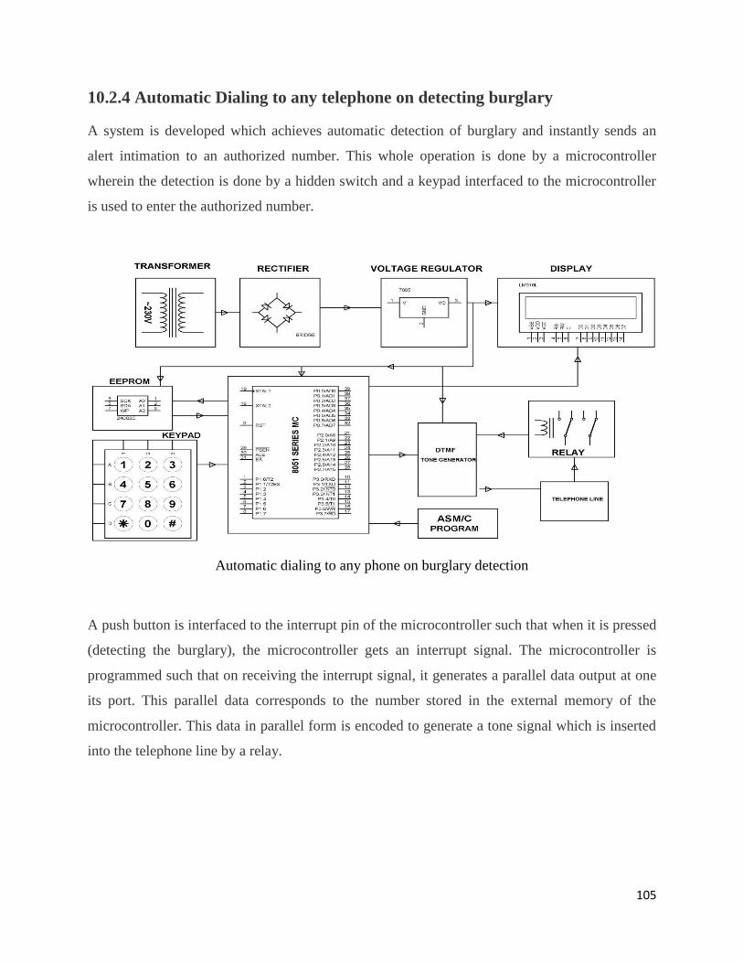
105
10.2.4 Automatic Dialing to any telephone on detecting burglary
A system is developed which achieves automatic detection of burglary and instantly sends an
alert intimation to an authorized number. This whole operation is done by a microcontroller
wherein the detection is done by a hidden switch and a keypad interfaced to the microcontroller
is used to enter the authorized number.
Automatic dialing to any phone on burglary detection
A push button is interfaced to the interrupt pin of the microcontroller such that when it is pressed
(detecting the burglary), the microcontroller gets an interrupt signal. The microcontroller is
programmed such that on receiving the interrupt signal, it generates a parallel data output at one
its port. This parallel data corresponds to the number stored in the external memory of the
microcontroller. This data in parallel form is encoded to generate a tone signal which is inserted
into the telephone line by a relay.
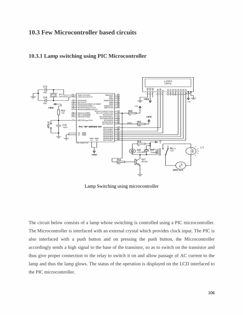
106
10.3 Few Microcontroller based circuits
10.3.1 Lamp switching using PIC Microcontroller
Lamp Switching using microcontroller
The circuit below consists of a lamp whose switching is controlled using a PIC microcontroller.
The Microcontroller is interfaced with an external crystal which provides clock input. The PIC is
also interfaced with a push button and on pressing the push button, the Microcontroller
accordingly sends a high signal to the base of the transistor, so as to switch on the transistor and
thus give proper connection to the relay to switch it on and allow passage of AC current to the
lamp and thus the lamp glows. The status of the operation is displayed on the LCD interfaced to
the PIC microcontroller.
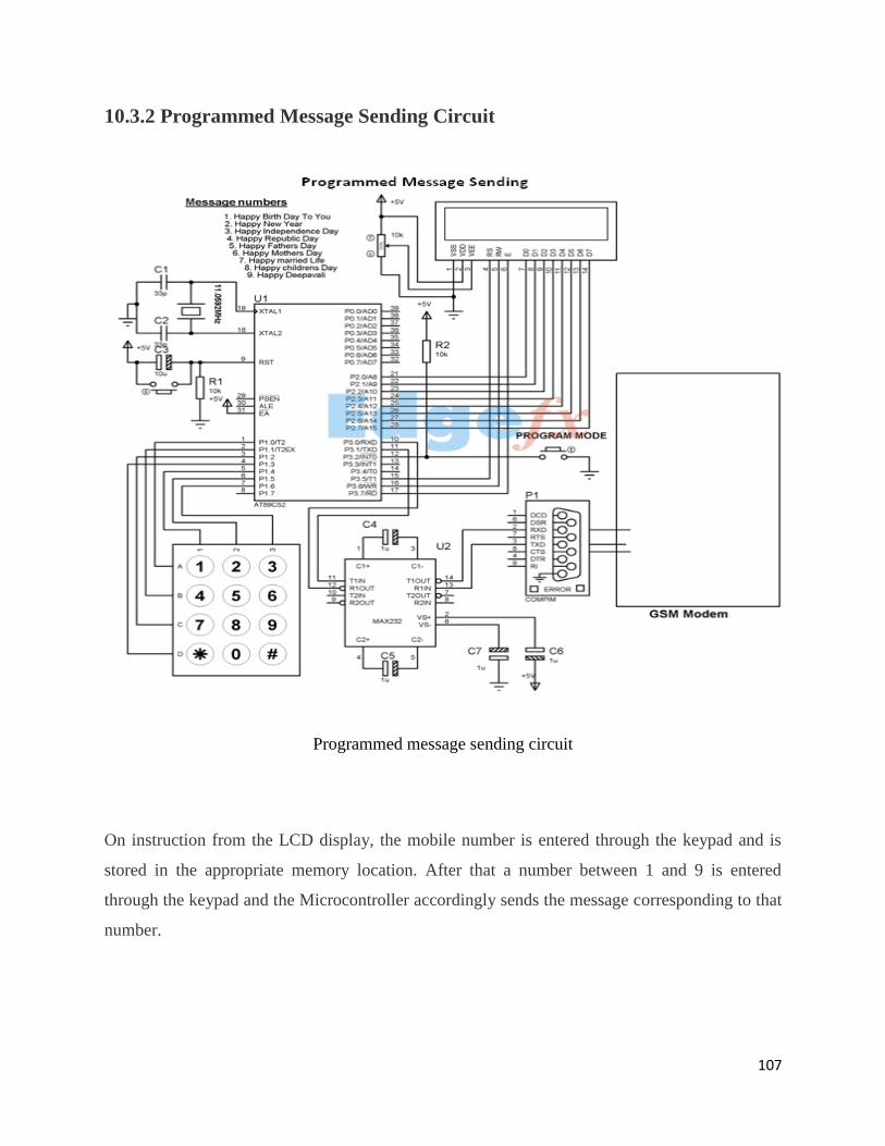
107
10.3.2 Programmed Message Sending Circuit
Programmed message sending circuit
On instruction from the LCD display, the mobile number is entered through the keypad and is
stored in the appropriate memory location. After that a number between 1 and 9 is entered
through the keypad and the Microcontroller accordingly sends the message corresponding to that
number.
108
The message is send to the GSM modem through the RS 232 connector and the level shifter IC
arrangement which transmits the message to the given mobile number. The whole operation is
accordingly displayed on the LCD display.
After some time, the message “ GSM based message sending System” Is displayed and when
program button is entered, the display changes to the message-“Enter mobile number” After
entering the mobile number # is pressed that prompts to enter the message number. After putting
the message number and then # pressed again indicates that “message sending” and then displays
“message sent” after sometime and then resumes back to normal display.
If you are not getting any of these message means that SIM card is not getting signal / network
not available.
Standard power supply of 12 volt DC and 5 volt through a regulator are made from a step down
12 v transformer along with a bridge rectifier and filter capacitor.
10.3.3 Intra system communication in automobiles
In this application, we follow a CAN (Control Area Network) concept, generally used in cars,
automobiles and industries. As the name implies control area network means that microcontroller
is connected in a network fashion like computers so that it can exchange data among themselves.
Here we are using 2 microcontrollers connected in a network fashion by a pair of wire connected
to pin 10 and 11(i.e., P3.0, P3.1) of port 3 of each microcontroller pins for the transmission and
reception of data among themselves with the help of RS232 serial communication using a pair of
wire. The first microcontroller is interfaced to 4×3 matrix keypad, which is connected to input
ports of first microcontroller. The second microcontroller is interfaced to an LCD display to
receive data from the first microcontroller. A 16 by 2 LCD is used to display 16 characters in
two lines.
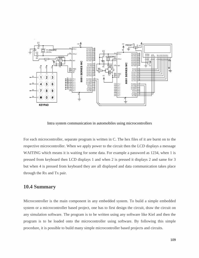
109
Intra system communication in automobiles using microcontrollers
For each microcontroller, separate program is written in C. The hex files of it are burnt on to the
respective microcontroller. When we apply power to the circuit then the LCD displays a message
WAITING which means it is waiting for some data. For example a password as 1234, when 1 is
pressed from keyboard then LCD displays 1 and when 2 is pressed it displays 2 and same for 3
but when 4 is pressed from keyboard they are all displayed and data communication takes place
through the Rx and Tx pair.
10.4 Summary
Microcontroller is the main component in any embedded system. To build a simple embedded
system or a microcontroller based project, one has to first design the circuit, draw the circuit on
any simulation software. The program is to be written using any software like Kiel and then the
program is to be loaded onto the microcontroller using software. By following this simple
procedure, it is possible to build many simple microcontroller based projects and circuits.

110
Ending Stuff
About the authors
The credit for each and every information given in this book goes to the team of Edgefx. We the
team of Edgefx , have been the pioneers in providing technical solutions and project kits to
millions of engineering students around the globe, since 1997. The credit for the projects and the
circuits goes to the technical team of Edgefx.
Right to readers
This book is intended to give relevant knowledge about microcontrollers, to the readers in the
simplest and basic way. Any person interested in this book has the authority to download, reprint
and distribute this book. However no person is given the permission to make any modifications
or alternations to the book and use it for his/her own monetary profit.
Legal Info
The copy right for the content and few images is solely authorized to the team of Edgefx. The
information written in each and every chapter is written based on relevant research and inputs by
the team of authors. The projects and circuits mentioned in the last chapter are the properties of
Edgefx team and are fully tested and authenticated.
Ways to interact with the team
If you are engineering student, looking for projects, feel free to click on the link given below:-
http://www.edgefxkits.in
111
If you want to look for technical solutions and information on any topic relevant to electronics,
electrical, robotics and communication, click on the link given below:-
http://www.elprocus.com/
You can also contact us at social media by liking our facebook pages
https://www.facebook.com/edgefx
https://www.facebook.com/elprocus