Embed Size (px)
Citation preview

MICRODISCHARGE-BASED PRESSURE CONTROLLING DEVICES AND THEIR APPLICATIONS TO CHEMICAL
SENSING IN HARSH ENVIRONMENTS
by
Scott Andrew Wright
A dissertation submitted in partial fulfillment of the requirements for the degree of
Doctor of Philosophy (Electrical Engineering)
in The University of Michigan 2009
Doctoral Committee:
Professor Yogesh B. Gianchandani, Chair Professor Brian E. Gilchrist Professor Khalil Najafi Associate Professor John E. Foster
Associate Professor Euisik Yoon

© Scott Andrew Wright
All rights reserved
2009

ii
DEDICATION
To Mom and Ray.

iii
ACKNOWLEDGEMENTS
First of all I would like to thank my family. My parents Chris and Ray King, and
Tina and Jim Wright, my sister Amanda Wilson, my grandparents Lucille and Stan
Davis, and Elizabeth and Larry Wright, and my great-uncle Sumner Davis. These
individuals have supported me throughout my life and academic career, for which I am
eternally grateful.
I would like to thank my advisor, Yogesh Gianchandani. He has dedicated
countless hours not only to our academic progress, but to teaching me as an individual to
perform and publish research. I would like to thank the professors at the University of
Michigan, including Professor Kensall Wise and my thesis committee: Professors Khalil
Najafi, Brian Gilchrist, Euisik Yoon, and John Foster for all of their help and guidance.
I would like to thank the WIMS, SSEL, and LNF staff including: Brendan Casey,
Dennis Schweiger, Robert Gordenker, Sandrine Martin, Ed Tang, and Trasa Burkhardt.
I would like to thank my group members, lab mates, and friends at the University
of Michigan and in Ann Arbor. They have always been there for me, providing help and
making my time at Michigan enjoyable. This group includes: Allan Evans, Christine
Eun, Mark Richardson, Jong Park, Bhaskar Mitra, Angelo Gaitas, Naveen Gupta, Scott
Green, Tao Li, Weibin Zhu, Richard Fung, Amar Basu, Karthik Visvanathan, Kabir
Udeshi, Senol Mutlu, Ken Takahata, Tzeno Galchev, Niloufar Ghafouri, Amir Borna,
Erkan Aktakka, Ali Besharatian, Andy Gross, Seow Yuen Yee, Jeff Gregory, Jae Yoong
Cho, Sang Won Yoon, Sang-Hyun Lee, Jay Mitchell, Hanseup Kim, Sang Woo Lee,
Andrew Kuo, Neil Welch, Ruba Borno, Tushar Bansal, Gayatri Perlin, Razi Haque,
Angelique Johnson, Emine Cagin, Kim Khalsa, Shahrzad Naraghi, Becki Veeneman,
Awlok Josan, Kiran Pandey, Kwan Tan, Mark Ferriss, Jeff Siddiqui, Danese Joiner,
Elizabeth Hansson, Jamey Lister, Marc Siciliano, Carl Grant, Charles Doriean, and
Michael McCorquodale.
I am grateful for all of you.

iv
TABLE OF CONTENTS
DEDICATION .................................................................................................................... ii
ACKNOWLEDGEMENTS ............................................................................................... iii
LIST OF FIGURES .......................................................................................................... vii
LIST OF TABLES ........................................................................................................... xiv
LIST OF APPENDICIES ................................................................................................. xv
ABSTRACT .................................................................................................................... xvii
CHAPTER 1 INTRODUCTION ........................................................................................ 1
1.1 Electrical Breakdown in Gases ......................................................................... 2 1.2 Uses of Macroscale Plasmas ............................................................................. 8 1.3 Microdischarges .............................................................................................. 11
1.3.1 Calculated Steady State Parameters ...................................................... 14 1.3.2 Microdischarge Modeling ..................................................................... 16
1.4 Types of Microdischarges ............................................................................... 17 1.4.1 Dielectric Barrier Discharge ................................................................. 17 1.4.2 Microhollow Cathode Discharge .......................................................... 18 1.4.3 Inductively Coupled Microplasma ....................................................... 19 1.4.4 Planar Discharge ................................................................................... 20 1.4.5 Parallel Plate Discharge ........................................................................ 21
1.5 Microdischarge Devices .................................................................................. 21 1.5.1 Display Technology .............................................................................. 21 1.5.2 Microdischarges for Chemical Analysis ............................................... 22 1.5.3 Other Microdischarge Devices ............................................................. 23
1.6 Microdischarge-Based Microtransducers ....................................................... 23 1.6.1 Vacuum Generation Using Microdischarges ........................................ 24 1.6.2 Pressure Sensing Using Microdischarges ............................................. 26 1.6.3 Chemical Sensing Microsystem ........................................................... 29
1.7 Organization of Thesis .................................................................................... 32

v
CHAPTER 2 VACUUM GENERATION USING MICRODISCHARGES ................... 34
2.1 Background ..................................................................................................... 35 2.2 Device Concept and Operation ....................................................................... 40 2.3 Theoretical Considerations ............................................................................. 44 2.4 Design and Fabrication ................................................................................... 57 2.5 Experimental and Modeling Results ............................................................... 60
2.5.1 Removing Air from Microelectronic Packages .................................... 60 2.5.2 Pressure Reduction Behavior ................................................................ 64 2.5.3 Operating Micro-SIPs at Lower Pressures ........................................... 67 2.5.4 Relationship between Discharge Gap Spacing, Pressure, and Air Removal Rate ................................................................................................. 67 2.5.5 Removal Rates of Various Gases ......................................................... 69 2.5.6 Removal Rate of Water Vapor ............................................................. 72 2.5.7 Pulsed Discharge Operation ................................................................. 74 2.5.8 Thermally Assisted Discharges ............................................................ 76
2.6 X-Ray Photoelectron Spectroscopy Results ................................................... 77
CHAPTER 3 PRESSURE SENSING USING MICRODISCHARGES .......................... 79
3.1 Background ..................................................................................................... 79 3.2 Device Concept and Operation ....................................................................... 83
3.2.1 Pulsed Discharges ................................................................................. 86 3.2.2 Current Pulse Operation and Simulation .............................................. 87
3.3 Design and Fabrication ................................................................................... 91 3.4 Experimental Results ...................................................................................... 94 3.5 Discussion of Results .................................................................................... 104
CHAPTER 4 CHEMICAL SENSING MICROSYSTEM .............................................. 106
4.1 Background ................................................................................................... 107 4.2 Detrimental Effect of Contaminant Nitrogen in Spectral Chemical Sensing 116
4.2.1 Background ......................................................................................... 116 4.2.2 Resulting Spectra in SF6 ..................................................................... 117
4.3 Using Micro-SIPs for Gas Purification ......................................................... 122 4.3.1 Concept, Operation, and Design of Gas Purifying Micro-SIPs .......... 122 4.3.2 Results and Discussion ....................................................................... 124
4.4 Harsh Environment Chemical Sensor ........................................................... 126 4.4.1 System Concept .................................................................................. 126 4.4.2 System Optical Emission Sensor ........................................................ 127 4.4.3 System Bidirectional Micromachined Valves .................................... 129 4.4.4 System Operation and Fabrication ...................................................... 130

vi
4.4.5 Results and Discussion ....................................................................... 132
CHAPTER 5 CONCLUSION......................................................................................... 134
5.1 Dissertation Summary ................................................................................... 134 5.2 Suggestions for Future Work ........................................................................ 137
5.2.1 Utilizing Micro-SIPs to Reach High Vacuum (10-6 Torr) .................. 137 5.2.2 Harsh Environment Chemical Sensor Packaging ............................... 141 5.2.3 Selective Growth of Doped Nanowires Using Microdischarges ........ 142
APPENDICES ................................................................................................................ 143
BIBLIOGRAPHY ........................................................................................................... 192

vii
LIST OF FIGURES
Figure 1.1: Paschen curves for discharges created between copper parallel plate electrodes in various gases. .......................................................................................... 4
Figure 1.2: Paschen curves for parallel and planar electrodes with 500 µm spacing [Wil03b]. .................................................................................................................... 12
Figure 1.3: Schematic diagrams of the (a) volume discharge and (b) surface discharge DBD. .......................................................................................................................... 18
Figure 1.4: Schematic diagram of the microhollow cathode discharge configuration. ... 19
Figure 1.5: Schematic diagram of typical planar electrodes and planar microdischarge. 20
Figure 1.6: Schematic diagram of typical parallel plate electrodes and microdischarge. . 21
Figure 1.7: Plot of required device operating temperature vs. fabrication complexity for several pressure reducing devices. (See table for the list of abbreviations and references.) ................................................................................................................. 26
Figure 1.8: Plot of maximum operating temperature vs. fabrication steps for various high temperature pressure sensors. (See table for the list of abbreviations and references.) ................................................................................................................................... 29
Figure 1.9: Plot of operating temperature range vs. number of detectable chemical species for various high temperature gas sensors. (See table for the list of abbreviations and references.) ................................................................................... 32
Figure 2.1: Illustration of NEG isolation from micromachined device in a microscale package. ..................................................................................................................... 37
Figure 2.2: Plot of required device operating temperature vs. fabrication complexity for several pressure reducing devices. (See table for the list of abbreviations and references.) ................................................................................................................. 40
Figure 2.3: Schematic of a commercial package, commercial pressure sensor, micro-SIP, power, and readout circuitry. RB1 and RB2 are ballast resistors of varied resistance which limit the current flowing between the anode and cathode. ............................. 40

viii
Figure 2.4: Schematics of micro-SIP electrodes: (a) basic design, top view, (b) heated cathode design, top view, and (c) side view. ............................................................. 41
Figure 2.5: Modeled electric field strengths normal to a version 2 micro-SIP surface at a height of 50 µm above the electrodes. ....................................................................... 56
Figure 2.6: (a) Version 2 chip with a single anode and eight cathodes. (b) Version 3 chip with a single anode and two cathodes, each having 15 discharge gaps. (c) Version 4 chip with high current density. (d) Version 5 chip with low current density. .......... 58
Figure 2.7: A commercial package after opening, with two commercial pressure sensors and three different micro-SIP versions. ..................................................................... 60
Figure 2.8: Pressure drop in a 6.33 cm3 package over time. Fifteen consecutive 10 minute discharges drop the pressure 168 Torr. The pressure remains stable over periods of 10 hours of micro-SIP inactivity and returns to atmospheric pressure when the package is opened. ............................................................................................... 62
Figure 2.9: Pressure drop, shown in Fig. 2.8, as a function of cumulative energy supplied to the discharge with an initial pressure of 760 Torr. The upper and lower trend lines, respectively, show the pressure readings when the discharge is interrupted (causing spikes as the pressure stabilizes without an increase in energy) and when the discharge remains on. The corresponding number of gas molecules removed at room temperature, and the fraction of the package volume evacuated, are noted on the second Y axis. ............................................................................................................. 63
Figure 2.10: Pressure drop in a 4.0 cm3 package over 30 minutes of micro-SIP operation, starting at an initial pressure of 31 Torr. .................................................................... 63
Figure 2.11: Micro-SIP electrodes displaying remains of a cathode after reactive sputtering, illustrating areas of complete titanium sputtering. .................................. 66
Figure 2.12: (a) Experimentally measured (over 20 min.) and (b) theoretically determined pressure reduction rates in air as a function of discharge gap spacing and pressure. The micro-SIPs have between 35 µm and 150 µm discharge gaps, are operated with 1,500 V, have initial pressures between 100 Torr and 725 Torr, and are operated in a 4 cm3 package. ...................................................................................... 69
Figure 2.13: Spectrum of the micro-SIP electrode pair discharge in air indicating the dissociation of oxygen and ionization of titanium and nitrogen. ............................... 70
Figure 2.14: Change in pressure in environments of pure oxygen, nitrogen, helium, and air. The micro-SIPs have 100 µm discharge gaps, are operated with 1,000 V, have initial pressures of 200 Torr, and are operated in a 4 cm3 package. This shows that the mixed gas air environment is removed at a rate between oxygen and nitrogen as expected, based on the different chemisorptions rates of the gases. Helium is not removed as it is an inert gas and does not bond with titanium. ................................. 72

ix
Figure 2.15: Schematic of the glass package, micro-SIP, and external equipment used to introduce and measure humidity removal. ................................................................. 73
Figure 2.16: Experimentally measured change in humidity using a micro-SIP. The micro-SIP has a 100 µm discharge gap, is operated with 1,000 V, has an initial pressure of 400 Torr, and is operated in a 4.0 cm3 glass package. A mechanical pump is used for comparison, starting at the same initial pressure and relative humidity. The micro-SIP removes more relative humidity than the mechanical pump when both reduced the pressure by 10 Torr. The heating and cooling transients are caused by the discharge induced heat from the micro-SIP. They are absent in the mechanical pump measurements due to the absence of a heat increase. ................... 74
Figure 2.17: Pulses of 1,000 V are applied at a frequency of 1 Hz. (a) Pressure reduction rate as a function of pulse duration, averaged over 20 minutes of gas removal. The longer pulse durations reduce pressure faster. The error bars indicate a standard deviation of removal rate. (b) Relative energy required to remove an arbitrary unit of pressure with different pulse durations, normalized to a DC discharge. Pulses are five times more energy efficient, but require a longer duration of time. ................... 75
Figure 2.18: Average pressure reduction rate comparison using micro-SIPs with thin-film heaters as cathodes. In the “hot” trials, the cathodes are heated through the application of the indicated average power, while in the “cold” trials; identical micro-SIPs with cathode heaters are not heated. The calculated average cathode temperatures are indicated. The heaters are all 50 μm in width and 1 mm or 2 mm in length. The micro-SIPs are operated with 1,000 V at initial pressures of 100 Torr and 200 Torr in a 1 cm3 package. .............................................................................. 77
Figure 3.1: Plot of maximum operating temperature vs. fabrication steps for various high temperature pressure sensors. (See table for the list of abbreviations and references.) ................................................................................................................................... 83
Figure 3.2: Schematic of (a) a Bulk Foil sensor with electrodes above a quartz chip, illustrating placement, and the microdischarge chamber during operation, and (b) a Planar sensor with microdischarge. ........................................................................... 85
Figure 3.3: Diagram of a microdischarge between a single anode and two cathodes in a Bulk Foil structure. .................................................................................................... 86
Figure 3.4: Circuit model for discharge. The pulse power source is represented by the discharging of the capacitor, C, that is switched on at time t = 0. The current pulse is represented as a series combination of an inductance, L, and resistance, R along the current path. Rs is a shunt resistance, which allows a small amount of secondary current to flow during the main current pulse. .......................................................... 88
Figure 3.5: Modeled (a) and experimentally measured (b) current pulses in cathodes 1 and 2 in a pressure sensor with electrodes spaced 50 µm apart, 1 mm in diameter, and 125 µm thick at 200 Torr. The modeled pulses are referred to as M1 and M2. .. 89

x
Figure 3.6: Fabrication processes for Bulk and Planar sensors. ....................................... 92
Figure 3.7: Bulk Foil sensors with (a) electrodes spaced 100 µm apart, 50 µm thick and (b) electrodes spaced 50 µm apart, 125 µm thick. Planar sensors with (c) three circular cathodes spaced 50 µm apart, 300 µm in width and (d) five straight cathodes spaced 50 µm apart, 50 µm in width. ........................................................................ 94
Figure 3.8: Pulse generating and readout circuitry used for sensor operation. ................ 95
Figure 3.9: Oscilloscope trace of the voltage pulses used for pressure measurements. The voltage was measured across 100 Ω resistors and used to calculate the current, with V1 as the voltage in cathode 1 and V2 as the voltage in cathode 2. ........................... 96
Figure 3.10: Measured current pulse peak values. (a) Sum of the pulse currents in two Bulk Foil cathodes as a function of pressure and temperature. The empirical curves for each temperature are indicated by the solid lines. (b) Temperature trend for equation terms C1 and C2 in the peak current equation. ............................................ 97
Figure 3.11: Percentage of total current in the cathodes at 1,000˚C in a Bulk Foil sensor with electrodes spaced 50 µm apart, 1 mm in diameter, and 125 µm thick. ............. 98
Figure 3.12: Differential current output determined from the percentage of total current in Bulk Foil sensors with electrodes (a) spaced 50 µm apart and (b) spaced 100 µm apart, 1 mm in diameter, and 125 µm thick. Each data point is the average of 100 measurements. The two empirical curves per temperature are indicated by the solid lines. ........................................................................................................................... 99
Figure 3.13: The average sensitivities in both the low and high pressure ranges for the Bulk Foil sensors in Fig. 3.12(a) and (b) as functions of temperature. ................... 100
Figure 3.14: Percentage of total current and differential current output in Planar sensors with (a) electrodes spaced 50 µm apart, 300 µm in width and (b) electrodes spaced 50 µm apart, 50 µm in width. Each data point is the average of 100 measurements. ................................................................................................................................. 103
Figure 4.1: Plot of operating temperature range vs. number of detectable chemical species for various high temperature gas sensors. (See table for the list of abbreviations and references.) ................................................................................. 113
Figure 4.2: (a) Plot of sensitivity vs. speed of detection for various kinds of chemical sensors (see table for the list of abbreviations and references). Each of the publications mentioned represent the best results of the various classes of devices. (b) Plot of selectivity vs. number of detectable chemical species for gases and organic compounds. L, M, and H represent a low, medium, and high number of chemicals [Mit08c]. ................................................................................................. 114
Figure 4.3: Microplasma emission spectra in air and SF6 at 3 Torr. All figures use the same arbitrary unit scale for the intensity. (a) SF6 environment with 800 V and 500

xi
μA. (b) SF6 environment with 1,000 V and 2.7 mA after the spectrum produced in air has been subtracted out. (c) Air environment with 500 V and 500 μA. (d) Average normalized difference between SF6 and air emission spectra recorded between 400 mTorr and 10 Torr. ............................................................................. 119
Figure 4.4: Emission spectra in (a) air and (b) SF6 between 400 nm and 510 nm where the molecular emission band produced by SF6 has been observed. Three consecutive measurements are averaged in each environment. .................................................. 121
Figure 4.5: Gas-purifying micro-SIPs. A DC voltage is applied to selectively remove nitrogen and oxygen. ............................................................................................... 124
Figure 4.6: Percentage of contaminants (nitrogen and oxygen) in a helium sample during gas purification, showing the thorough removal of the unwanted gases. ................ 125
Figure 4.7: Spectra of the pump discharge in 99.25% helium with air contamination at 200 Torr (a) before purification and (b) after purification. Small amounts of nitrogen cause intense emission lines compared to helium at time = 0, demonstrating the necessity of nitrogen removal. ................................................................................. 126
Figure 4.8: Schematic of the entire harsh environment chemical sensing system. ........ 127
Figure 4.9: Microdischarge optical emission sensor (chemical detector) used to detect carbon and other vapors through recorded spectra. (a) Schematic. (b) Photograph. ................................................................................................................................. 128
Figure 4.10: Microvalve concept: The valve consists of ceramic-PZT-Si-glass structure. A PZT stack actuator moves the silicon plate to open or close the valve. Micro-groove patterns are fabricated on the silicon plate to increase the flow area [Par08]. ................................................................................................................................. 130
Figure 4.11: System before sealing in ceramic package next to a U.S. penny. ............. 131
Figure 4.12: Ratio of carbon to nitrogen emission line intensity during gas purification at 200°C, based on their strongest emission lines. ...................................................... 132
Figure 4.13: Spectra of acetone sample backfilled with helium during gas purification at 200°C. (a) Spectrum recorded before purification, showing strong nitrogen emissions and low C2 emissions. (b) Spectrum recorded after purification, showing diminished nitrogen and increased CN and C2 emissions. ...................................... 133
Figure 5.1: Schematic of a micro-SIP and accompanying magnet in a sealed package with outlet ports. .............................................................................................................. 139
Figure 5.2: Schematic of harsh environment chemical sensor package with semi-permeable membrane and integrated fiber optic cable. ........................................... 142
Figure A1.1: Radii of microdischarges as a function of pressure and temperature. ....... 147

xii
Figure A1.2: Predicted electric field strength in a microdischarge-based pressure sensor with 50-µm gaps and 125-µm-thick electrodes. ...................................................... 158
Figure A2.1: The atomic composition of used anodes, cathodes, and fresh unused titanium electrodes. These are the only five elements found in the electrode surfaces. Broad spectra are examined and at least three spectra are averaged for each data point. ........................................................................................................................ 161
Figure A2.2: The distribution of oxygen, titanium and nitrogen based on the atomic composition of used anodes, cathodes, and fresh unused electrodes. Narrow, focused spectra are examined and at least three spectra are averaged for each data point. The figure only considers the concentration of these three elements in the sample. ...... 161
Figure A2.3: The atomic concentration of titanium and nitrogen in anodes and cathodes of micro-SIPs which had been operated at different initial pressures. .................... 162
Figure A2.4: The atomic concentration of oxygen in anodes and cathodes of micro-SIPs which had been operated at different initial pressures. ............................................ 162
Figure A3.1: Schematic diagram of a thermionic cathode with heating circuit. ........... 165
Figure A3.2: Emission current as a function of cathode temperature with two materials. ................................................................................................................................. 167
Figure A3.3: Emission current as a function of applied anode-cathode potential difference. ................................................................................................................ 169
Figure A4.1: Emission spectrum of pure SF6 produced in a RIE chamber. An excitation frequency of 13.56 MHz is used. Three consecutive measurements are averaged. 175
Figure A4.2: Schematic of electrodes and system set-up. ............................................. 177
Figure A5.1: Emission spectra produced in SF6 with different applied power. The stronger intensities are produced by applying 1,000 V and the weaker intensities are produced by applying 800 V. ................................................................................... 180
Figure A5.2: Emission spectra produced in SF6 at different pressures. The stronger intensities are produced at 5 Torr and the weaker intensities are produced at 10 Torr. ................................................................................................................................. 181
Figure A6.1: Layout with liquid tin in a ceramic crucible next to the substrate with a tungsten anode. ........................................................................................................ 185
Figure A6.2: Nanowires, approximately 50 nm in diameter and 10 µm in length. ....... 186
Figure A6.3: Gold particle at the tip of a nanowire, with additional particles in the background. The particle is measured as 55.7 nm in diameter. .............................. 187

xiii
Figure A6.4: Silicon substrate showing regions with and without nanowire growth. ... 187
Figure A6.5: Region of low nanowire growth, demonstrating sparse nanowire formation. ................................................................................................................................. 188
Figure A6.6: Resulting substrate exposed to a microdischarge with a high power density. ................................................................................................................................. 190

xiv
LIST OF TABLES
Table 1.1: Minimum breakdown voltage and pd value at which it occurs in various gases [Cob58]. ....................................................................................................................... 5
Table 1.2: DC glow microdischarge operating parameters in a microdischarge-based pressure sensor. .......................................................................................................... 15
Table 2.1: Calculated parameters for a micro-SIP with 50-µm discharge gaps and 1,500 V applied at a pressure of 100 Torr. .......................................................................... 57
Table 3.1: Typical performance of four different sensor designs with the highest performance in each category in bold. ..................................................................... 101
Table A1.1: DC glow microdischarge operating parameters in a microdischarge-based pressure sensor, calculated over the range of 10-2,000 Torr and 23-1,000ºC. ........ 146
Table A1.2: DC sheath operating parameters in a microdischarge-based pressure sensor, calculated over the range of 10-2,000 Torr and 23-1,000ºC. .................................. 148
Table A6.1: Parameters varied to determine the optimum environment for nanowire growth. ..................................................................................................................... 189

xv
LIST OF APPENDICIES
APPENDIX 1 CALCULATING MICRODISCHARGE PARAMETERS .................... 144
A1.1 Microdischarge Parameters in a Pressure Sensor ...................................... 145 A1.2 Breakdown Voltage.................................................................................... 148 A1.3 Primary Discharge...................................................................................... 149 A1.4 Cathode Sheath .......................................................................................... 154 A1.5 Other Current Generating Mechanisms ..................................................... 157
APPENDIX 2 X-RAY PHOTOELECTRON SPECTROSCOPY RESULTS ............... 159
A2.1 Measurement Description .......................................................................... 159 A2.2 Electrode Composition Results .................................................................. 160
APPENDIX 3 CONSIDERATIONS FOR A MICROSCALE ION GAUGE................ 164
A3.1 Macroscale Ion Gauges .............................................................................. 164 A3.2 Hot Cathode Ionization Gauges ................................................................. 165 A3.3 Cold Cathode Ionization Gauges ............................................................... 166 A3.4 Microscale Hot Cathode Ion Gauges ......................................................... 166 A3.5 Microscale Cold Cathode Ion Gauges ....................................................... 169 A3.6 Operating Pressure Range .......................................................................... 171 A3.7 Conclusion ................................................................................................. 172
APPENDIX 4 MICROPLASMA SF6 EMISSION LINE DETECTION ....................... 173
A4.1 SF6 Emission Spectrum Characterization .................................................. 173 A4.2 Experimental Setup .................................................................................... 176
APPENDIX 5 SF6 MICROPLASMA CHARACTERISTICS ....................................... 179
APPENDIX 6 INVESTIGATION INTO THE GROWTH OF DOPED NANOWIRES USING MICRODISCHARGES ..................................................................................... 182
A6.1 Introduction ................................................................................................ 182 A6.2 Setup........................................................................................................... 184

xvi
A6.3 Results ........................................................................................................ 186 A6.4 Conclusions ................................................................................................ 190

xvii
ABSTRACT
MICRODISCHARGE-BASED PRESSURE CONTROLLING DEVICES AND THEIR APPLICATIONS TO CHEMICAL
SENSING IN HARSH ENVIRONMENTS
by
Scott Andrew Wright
Chair: Yogesh B. Gianchandani
Microdischarges offer an alternative and often advantageous sensing and
actuation method that has not been significantly exploited in microtransducers. This
thesis explores the capabilities of microdischarges to address problems such as cavity
pressure control, cavity pressure detection, and purity control of fill gases, which are
relevant to microsystems. Microdischarge-based transducers have been developed for
these purposes. One interesting aspect of microdischarge-based transducers is the wide
latitude of operating temperatures, as they are advantageous for room and high
temperature operation.
On-chip sputter-ion pumps control the pressure and gas purity in cavities. They
consist of thin-film titanium electrodes patterned on glass substrates. Microdischarges
sputter the cathodes, resulting in the selective chemisorption of titanium-reactive gases.
Using DC discharges, these devices have reduced the pressure by 168 Torr in an air-
filled, hermetically sealed, 6.33 cm3 package. Starting at 200 Torr, the pressure reduction

xviii
rate of air is 7.2 Torr/h; oxygen 11.5 Torr/h, and nitrogen 3.4 Torr/h. Relative humidity
is reduced at 6%/h. The pumps do not remove helium, purifying gas environments by
selectively removing contaminating nitrogen and oxygen. A theoretical model outlining
the dependency of gas removal rates on microdischarge parameters is presented.
Microdischarge-based pressure sensors operate by correlating the measured
change in spatial current distribution of pulsed DC microdischarges with pressure. One
sensor version uses three-dimensional arrays of horizontal bulk metal electrodes
embedded in quartz substrates with electrode diameters of 1-2 mm and 50-100 µm inter-
electrode spacing. These devices have been operated over 10-2,000 Torr, at temperatures
as high as 1,000˚C. The maximum measured sensitivity is 5,420 ppm/Torr, while the
minimum temperature coefficient of sensitivity is -550 ppm/K. Sensors of a second
version use planar electrodes, with 0.13 mm2 active areas.
To explore the utility of pressure controlling devices, these transducers are
combined with an optical emission sensor to create a high temperature gas phase
chemical detection microsystem. The microdischarge-based pressure sensor determines
the sample and backfilling gas pressure while the microscale-sputter-ion pump purifies
the gas environment. The contaminating nitrogen concentration has been reduced by
56.5x relative to helium and the spectral detection limit has been improved by 8x for
carbon at 200°C.

1
CHAPTER 1
INTRODUCTION
The utility derived from macroscale plasmas combined with current
microfabrication techniques has allowed for the development of microscale devices
which use microdischarges for operation. Microdischarge is the term applied to a small,
localized plasma region which, due to its size, demonstrate characteristics different from
those of plasma regions created on a larger scale [Wil03a, Kus05, Foe06]. Microplasma
is another term used to describe a microdischarge, but is typically used to describe a low
pressure glow discharge as opposed to the more general category.
Microdischarge-based transducers offer many advantages over their macroscale
counterparts, some result directly from the characteristics of microdischarges. One
advantageous characteristic is the ability to operate at pressures higher than atmosphere.
Additionally, microdischarge-based devices consume less power, which combined with
their small size, light weight, and low gas volume requirement, provides for the
possibility of use in portable, battery-operated microinstruments. Portable instruments
allow for real-time analysis in the field, without bringing samples to a laboratory.
Additionally, microdischarge-based devices may be embedded within other instruments
and numerous devices may be operated in parallel, due to their small size. One potential
instance of this is the use of microdischarge-based chemical sensors as detectors for gas

2
chromatography (GC) systems. Finally, if microdischarge-based devices are
microfabricated they can be mass-produced, making individual devices cheap.
A few forms of microdischarges have been utilized in microscale devices in the
past, but this thesis presents the use of DC and pulsed DC microdischarges for pressure
control, primarily in sealed packages or microsystems, which includes pressure sensing
and actuation.
Section 1.1 presents a qualitative review of electrical breakdown and various
discharge types. Section 1.2 presents a discussion of the uses of macroscale plasmas in
semiconductor processing and high vacuum pumps. Section 1.3 presents the operation of
microdischarges and the differences between them and their macroscale counterparts.
Section 1.4 presents several different microdischarge modes of operation. Section 1.5
presents various devices that use microdischarges. Section 1.6 presents the motivation
behind the development of, and contributions derived from, microscale-sputter-ion
pumps, high temperature microdischarge-based pressure sensors, and high temperature
chemical sensors. This section also contains brief comparisons to other technologies.
Section 1.7 presents the organization of this thesis.
1.1 ELECTRICAL BREAKDOWN IN GASES
Plasmas are characterized by charged ions and negatively charged electrons in
background neutral environments. They are created when energy is applied to a non-
conducting material, typically a neutral gas, causing the ionization of gas molecules and
the generation of free electrons. To form a plasma the neutral gas “breaks down” as the
ions and electrons undergo a multiplication process in which the gain from ionization

3
exceeds the net loss from processes such as diffusion, recombination, and attachment.
The initiation of this breakdown allows current to flow through though the plasma
regions, via the movement of the charged particles. Breakdown induces atomic
transitions, resulting in emissions which can often be visually observed. Breakdown can
occur through the application of high frequency and/or DC voltages, but this thesis focus
on the creation of DC plasmas and DC breakdown will thus be primarily discussed.
Faraday was the first to outline the properties of ionized gas [Far1839, Far1844, Far1855]
and the word plasma was later used by Langmuir and Tonks [Lan29]. For a more
detailed description of macroscale gas discharge physics, the reader is referred to
[Cob58], [Lie94], and [Rai97].
When an external DC field is applied between electrodes in a gas environment,
electrons are drawn from the lower potential cathode electrode(s) to the higher potential
anode electrode(s). If the applied voltage is low, carrier multiplication is insufficient to
produce a self-sustained discharge and random current bursts occur. When the external
field is greater than the “breakdown voltage”, breakdown occurs and a self-sustained DC
discharge is created which does not require an external ionizing source. In this discharge
the electrons collide with gas molecules and produce positive ions, which subsequently
drift to the cathode. Upon cathode impact, the energetic ions eject high energy
“secondary electrons” from the cathode, which sustain DC discharges by ionizing
additional neutral molecules. This “avalanche breakdown” process continues until an
appreciable level of ionization is reached (typically an ionization of above 10-8
ions/atoms [Rai97]). A positively charged “sheath” region at the cathode with high
electric fields is formed with a high density of ions.

4
The breakdown voltage is a function of the product of pressure (p) and electrode
spacing (d) according to Paschen’s law and is estimated as [Cob58]
lnln(1/ )
BDBpdVApd
γ
=⎡ ⎤⎢ ⎥⎣ ⎦
, (1.1)
where A and B are gas dependent constants and γ is the second Townsend ionization
coefficient. The relationships between the breakdown voltages and the pd products are
described by Paschen curves, which are shown in Fig. 1.1 for discharges between copper
parallel plate electrodes in various gas environments.
pd (mm Torr)0 5 10 15 20 25 300
200
400
600
800
1000
1200
Bre
akdo
wn
Volta
ge (V
)
Air
N2Ar
H2
He
Figure 1.1: Paschen curves for discharges created between copper parallel plate electrodes in various gases.
The breakdown voltage reaches a minimum for a given optimal value of the
product pd as shown in each Paschen curve. The minimum occurs at a pressure where
the electron mean free path is similar to the distance between electrodes. At lower pd
values, the breakdown voltage increases as the electrons undergo fewer collisions and

5
thus have a smaller chance of producing an ionizing collision. At higher pd values, the
breakdown voltage also increases as the mean free path length decreases, which
decreases the energy gained by the ions between collisions. Both instances necessitate a
higher electric field to initiate avalanche breakdown. The minimum breakdown voltage
can be calculated as
min12.718 lnBD
BVA γ
= . (1.2)
Table 1.1 presents the minimum breakdown voltage and the corresponding pd value at
which it is achieved in various gas environments. Discharges preferentially form at a
distance between electrodes which minimizes the pd product for a given pressure.
Table 1.1: Minimum breakdown voltage and pd value at which it occurs in various gases [Cob58].
Gas VBDmin pd cm·Torr Air 327 0.567 Ar 137 0.9 H2 273 1.15 He 156 4.0
CO2 420 0.51 N2 251 0.67
N2O 418 0.5 O2 450 0.7
Na (vapor) 335 0.04 SO2 457 0.33 H2S 414 0.6
DC discharges typically take the steady state form of glow or arc discharges.
Glow discharges occur at lower pressures with lower current densities while higher
current densities, which can be caused by a high ambient pressure, result in arc

6
discharges. The discharges are sometimes initiated by high current arcs, before a glow or
arc discharge is formed. These discharge types and sparks will be discussed individually.
Applying a voltage greater than the breakdown voltage creates a transition from
the Townsend, or “dark” discharge to a glow discharge. The glow discharge has a high
level of ionization, which results in an inhomogeneous electric field concentrated over
the cathode. After the initial formation of the glow discharge, it requires a lower applied
voltage to be sustained. The discharge is accompanied by a bright optical emission,
caused by atoms and ions excited to higher energy states through collisions with
energetic electrons. These photons created by atomic energy level transitions can then
induce secondary electrons through photoemission when they impinge upon the cathode,
especially when using low work function electrodes. The glow discharge is a non-
equilibrium or “low temperature” plasma, with the average electron temperature much
higher than the average ion temperature. The ion temperature is almost in thermal
equilibrium with the ambient gas environment. The cathode temperature does not
significantly change, allowing the glow discharge to be categorized as cold-cathode
discharge. The discharge is also referred to as a weakly ionized discharge as the plasma
density is only a small fraction of the neutral gas density
Glow discharges are classified as normal or abnormal discharges. The normal
discharge has a constant current density at the cathode. When the power to the discharge
is varied, only the area over which the glow exists varies, while the current density is
constant throughout the glow. After the entire cathode is enveloped within the glow, the
current density increases. This is known as the abnormal or anomalous glow discharge,
and requires relatively large increases in the applied voltage to cause small increases in

7
the current density. As the current density increases, it is accompanied by a decrease in
cathode sheath thickness, leading to a higher electric field and voltage drop in the sheath,
which increases the positive ion energy. The increased energy of the incoming positive
ions raises the temperature of the cathode, assuming the cathode is not cooled, causing
increased “thermionic emission”. Thermionic emission is the flow of charge carriers,
typically electrons, from a surface resulting when the thermal vibrational energy
overcomes the electrostatic forces restraining the carriers. A positive feedback can occur,
which can lead to the formation of an arc discharge.
A high current density results in an arc discharge, characterized by a high current
and low voltage. The arc voltage is low as the source of electrons is thermionic emission
supplied by a localized region of high current density (and high temperature) on the
cathode. This thermionic emission reduces the need for considerable field amplification
necessary in the glow discharge. When low boiling point metals are used, such as
copper, iron, and silver, the arc is anchored on localized hotspots on the cathode surface,
which can reach temperatures of 2,000–4,000 K. However, these high temperatures
cause rapid cathode erosion which in turn, cause the arc hotspots to shift rapidly. When
refractory materials (such as carbon or tungsten) are used, the arc is seen to be anchored
in a fixed location. The arc is referred to as a thermal or equilibrium plasma in which the
electrons, ions, and gas molecules are in thermal equilibrium, which is in contrast to the
glow discharge. This high gas temperature, high ionization rate, and high rate of exciting
collisions causes the arc discharge to have a much more intense emission compared to the
glow discharge. An arc discharge typically begins as a glow discharge, which degenerate
into an arc discharge as a result of thermal instabilities and high current densities.

8
In the spark discharge, breakdown is initiated through the Streamer mechanism.
This mechanism is fundamentally different from the Townsend mechanism, which
characterizes arc and glow discharges. The spark discharge consists of a single transient
avalanche trail, instead of a steady state discharge, and requires a large voltage. In an
electron avalanche, the number of electrons and ions increases exponentially with
distance. If the discharge gap is large, a single avalanche can result in an appreciable
level of ionization. Consequently, the path of a single avalanche can create an advancing
“spark channel”, which glows brightly due to the large number of highly energetic
electrons. When the avalanche reaches the anode, a spark channel full of positive ions
remains (the positive ions are assumed to be stationary for the duration of the avalanche).
Additional avalanches are initiated near the spark channel from photoemission from the
initial avalanche. The electrons from these are pulled into the positive ion filled spark
channel. Since there is no source of electrons to sustain it, the spark discharge is a
transient discharge. Lightening is a typical example of such a discharge.
1.2 USES OF MACROSCALE PLASMAS
In conventional macroscale plasmas, DC discharges are infrequently used as high
frequency methods of initiating discharges, such as RF, permit the use of dielectric
elements, which prevent electrodes sputtering. Plasmas are used for a variety of purposes
on the macroscale including IC fabrication and pressure reduction. Inert plasmas are
used in the sputter deposition of thin films and in the removal of films from wafers.
Chemically reactive plasmas are used in the deposition of silicon and dielectrics, as well
as in the chemical etching of various thin films. Several different types of plasma

9
systems are used to implement these semiconductor fabrication techniques. Parallel plate
reactors are commonly used for etching and operate through the application of a RF
voltage to two electrodes, one of which is attached to a capacitor [Lie94]. Electrons are
accelerated towards the electrode coupled to the capacitor faster than ions, causing a
negative bias on this electrode which influences ion directionality. Inductively coupled
plasmas (ICPs) use an external RF coil to inductively heat the plasma and increase
ionization. This increases the plasma density and etch rate without increasing substrate
damage relative to a parallel plate reactor [Lie94]. Electron-cyclotron reactors (ECRs)
use a magnetic field, which cause particles to move in circular trajectories, heating the
plasma. All of these macroscale plasmas are created in relatively large chambers, as
opposed to being created in localized regions of the wafers undergoing processing.
In addition to the various plasmas used for IC fabrication, macroscale plasmas are
used for pressure reduction in the general class of ion pumps. Titanium sublimation
pumps (TSPs), orbitron pumps, and sputter-ion pumps (SIPs) operate in high and
ultrahigh vacuum environments using titanium to getter gas molecules [Sch99, Wel01,
Wel03]. TSPs function by subliming a hot filament of titanium onto the inner walls of a
chamber where it chemisorbs impinging reactive gases. Orbitron pumps use electron
injectors to introduce electrons into an electrostatic field between two concentric
cylinders. The central cylinder is the anode, while the outer cylinder or wall serves as the
cathode. The electrons are injected with angular momenta and energies causing them to
miss the central anode and orbit it with long path lengths, on the order of several hundred
meters. Several variations have been developed. Diode pumps utilize the electrons to
heat and sublime bulk titanium partially surrounding the anode, and to ionize gas

10
molecules. The sublimed titanium coats the cathode, and the reactive gas ions are
absorbed and thus removed [Dou65]. Triode pumps use titanium on a separate cathode
which is sputtered by impinging ions. This coats the internal surfaces of the pump,
absorbing the impinging ions [Bil67, Den67]. Today, orbitron pumps function in a
manner similar to the triode pumps. The cavity wall (the cathode) is composed of
titanium into which ions are accelerated and entrapped. A titanium source is also
sputtered by electrons to replenish the cathode surfaces during pump operation.
Macroscale-SIPs operate through the creation of Penning discharges in externally
applied magnetic fields which are imposed axially to the discharges, crossing the electric
field, which cause electrons to move in long spiral paths during which they ionize gas
molecules. The ions are then accelerated toward the cathodes, both diffusing into it and
sputter fresh titanium onto the surrounding walls and anode. Gas molecules chemically
combine with this titanium to form solid compounds, removing the gas from the
environment and reducing the pressure. The gas diffusing into the cathode is eventually
reemitted, except for hydrogen which diffuses into the cathode bulk. Titanium is
traditionally used as it is chemically reactive with most gases including nitrogen and
oxygen [Hol59, Den67, Col94, Sch99, Mat01, Wel03]. Heavy nonreactive gases can also
be confined as they are buried by the deposited materials [Hol59, Sch99, Mat01, Wel03].
To improve trapping of nonreactive gases, noble diode pumps utilize tantalum and triode
pumps utilize more complex geometries. These pumps traditionally have pumping rates
of 0.3-2 liters/second and can operate between 400 and 40,000 hours, depending on the
pressure [Sch99]. The pumping speed increases with pressure as the number of ions
bombarding the cathode increases more than linearly:

11
I = kpn , (1.3)
where I is the ion current, k is a constant, p is the pressure, and n is between 1.05-1.2.
Macroscale-sputter-ion pumps approximately 3 cm in length and 0.3 kg in weight
are commercially available, but these devices are significantly larger than the pumps
described in this thesis [Rut99, Var08].
1.3 MICRODISCHARGES
Microdischarges demonstrate characteristics different from those of plasma
regions created on a larger scale. Macroscale plasmas tend to be unstable and susceptible
to arcs at higher pressures, including atmospheric pressure, which limits their use.
Microdischarges however, can exist at high pressures due to the small distance between
electrodes. Paschen’s law, Section 1.1, describes this favorable so-called pd scaling
which allows microdischarges to be formed with relatively low applied voltages at high
pressures between closely spaced electrodes. Lower applied voltages reduce the current
densities in the sheath region, which reduces instabilities and arc formation.
In certain microdischarges multiple path lengths are simultaneously available
between electrodes, which makes the discharge gap a variable and permits a low
breakdown voltage to be sustained, even as the pressure changes from the value that
favors the minimum electrode spacing [Wil03b]. This is shown in Fig. 1.2, which
compares the conventional Paschen curve for parallel plate electrodes and the measured
breakdown voltage for planar electrodes spaced 500 µm apart at their nearest edges. The
coplanar electrodes are 1 µm thick Al on 20 µm polyimide patterned on a silicon wafer.

12
Figure 1.2: Paschen curves for parallel and planar electrodes with 500 µm spacing [Wil03b].
In addition to functioning at high pressures, microdischarges experience much
higher power densities, voltage gradients, and electric field strengths in their space charge
or sheath region compared to their macroscale counterparts when similar voltages are
applied [Wil03a, Ede05, Kus05, Foe06, Cho07]. This allows ions to gain signification
energy to induce secondary electron emission and sputtering at pressures exceeding
atmosphere. Most of the voltage drop in microdischarges is across the sheath, where the
electrons are accelerated to high energies due to the strong electric field. In
microdischarges, the width of the sheath and the size of the microdischarge can be similar
[Kus05]. They can also be on the same scale as the Debye length, which is the
characteristic length scale in a plasma and the distance scale over which significant
charge densities can exist. This can impact the ability of the discharge to utilize the full
electrode geometry. Power densities of tens of kW-cm-3 to ≥ 1 MW-cm-3 are achieved in
microdischarges [Ede05, Kus05, Foe06]. Power densities of this magnitude are only

13
achieved on the macroscale by using pulsed biases. These variations from typical
macroscale behavior are due to small electrode sizes and discharge spacing.
A benefit of microdischarges is that they can exist as unbounded discharges,
where their size is determined by the electrode spacing, electrode shape, pressure, and
temperature as opposed to the volume of the spatial cavity in which they are generated.
DC microdischarges resemble normal or abnormal glow discharges, as they are
driven by high energy secondary electron emission with glow regions self-localized over
the cathodes. They resemble weakly ionized or low temperature plasma discharges as the
ions and neutral gas molecules in the discharge are near the ambient temperature and in
thermal equilibrium. Emission and absorption spectroscopic experiments reveal gas
temperatures only 100-150 K above the ambient [Ede05]. Despite the high collision rate
at pressures as high as atmosphere, the electrons are in non-equilibrium, as they have
much higher temperatures. In these weakly ionized plasmas, electron-electron and
electron-ion collisions can be ignored compared to electron-neutral collisions. In
addition the positive column, typically observed in macroscale plasmas, can be absent.
At higher operating pressures, microdischarges transition into high-temperature arcs or
microarcs.
Unlike traditional glow discharges, microdischarges additionally have a large
number of high energy “runaway electrons” with energies in excess of 100 eV at 1.2 Torr
[Wil03a, Kus05]. These electrons are referred to as “beam” electrons, which are
secondary electrons that are accelerated through the sheath without collisions while
attaining high energies. These electrons primarily drive microdischarges. Their high
energy creates a non-Maxwellian electron energy distribution in microdischarges

14
between the lower energy “bulk” electrons and the higher energy beam electrons
[Wil03a, Ede05, Cho07, Hon08]. (The distribution function in macroscale discharges is
typically assumed to be Maxwellian.) The bulk electrons have been found to have
temperatures of 5.5-6.0 eV near the cathode and 2-3 eV between the electrodes, near the
center of the discharge.
1.3.1 Calculated Steady State Parameters
To describe steady state DC microdischarges, the ionization frequency and other
parameters are calculated both in the discharge and in the sheath, which is situated at the
cathode. The parameters describing a DC, glow microdischarge in a microdischarge-
based pressure sensor (Chapter 3) under steady-state operation at 10 Torr and 23ºC are
shown in Table 1.2 to serve as a typical example. The microdischarge is created between
two planar parallel electrodes with an applied voltage of 1,000 V. The parallel electrodes
are spaced 50 µm apart. The microdischarge radius is measured along the axis parallel to
the electrodes. As the pressure is increased, the microdischarge does change from a
normal glow discharge to an abnormal glow discharge however, these discharge
mechanisms are similar, and similar analysis can be applied for the different regions of
operation unless the microdischarge transitions to a microarc [Cob58]. The plasma
density is found to be 8.5 x 1013 cm-3 at 10 Torr, which is similar to the modeling results
of an argon microdischarge at 50 Torr with an estimated density of 2 x 1013 cm-3 [Kus05].
See Appendix 1 for a detailed description of the parameters and derivations used to
describe steady state microdischarges, when operating as glow discharges.
Several parameters in the sheath and discharge can be compared to yield insight
concerning planar microdischarge operation. The ion density is slightly lower at the

15
sheath boundary, ns, than in the discharge, no, 7.4 x 1013 cm-3 vs. 8.5 x 1013 cm-3, due to
the ion density decrease in the “presheath”, which is situated between the discharge and
the sheath. The ion velocity is higher at the sheath boundary, us, 2,800 m/s vs. 700 m/s,
due to higher electric field in the sheath causing ion acceleration. However, as previously
mentioned, microdischarges have been found to have higher electric field strengths in the
sheath than predicted by traditional macroscale models [Mit08c].
Table 1.2: DC glow microdischarge operating parameters in a microdischarge-based pressure sensor.
Parameter Symbol Units Value at 23ºC and 10 Torr
Plasma Density no cm-3 8.5 x 10¹³
Debye Length λDe µm 1.4 Electron
Temperature Te eV 3
Electron Mobility µe m2/ V · s 3.5 Electron Velocity ve m/s 1.2 x 10⁶ Ion Temperature Ti eV 0.056
Ion Mobility µi m2/ V · s 2.9 x 10⁻²
Ion Velocity vi m/s 700 Ionization Rate νiz Hz 4 x 10⁷
Ion Diffusion Step Between
Collisions Li µm 3.7
Radius R µm 114 Electric Field
Strength E V/cm 340
Sheath Parameters Density at Sheath
Boundary ns cm-3 7.4 x 10¹³
Ion Velocity at Sheath Boundary us m/s 2,800
Current Density Jo A/cm2 3.3 x 10⁸
The ambient pressure and temperature affect microdischarges as well. As the
pressure increases, and as the temperature decreases, discharges become exponentially

16
more confined. The radius is decreased and the sheath is reduced in thickness. This
results in an increase in electric field strength, both in the discharge and in the sheath.
The current in a DC discharge is given by
( )2
0 1 0101
2discharge eRI en J Eπ χ μχ
⎛ ⎞= ⎜ ⎟
⎝ ⎠. (1.4)
1.3.2 Microdischarge Modeling
Several modeling techniques are used to model steady state microdischarges,
most of which concentrate on cylindrically symmetric structures with a central hole
through a metal-dielectric-metal sandwich stack [Foe06]. Modeling microdischarges is
complex due to the differences between macroscale plasmas and microdischarges. In
particular, considering the non-Maxwellian electron energy distribution function, which
is not considered in Section 1.3.1, improves model accuracy. Fluid models exist which
solve continuity, flux, and energy equations for separate species in the microdischarges
[Boe05]. A 2-D fluid model has been developed by Kushner which takes into account
both low energy bulk and high energy beam electrons and their position at various time
steps [Kus05]. The model uses a Monte Carlo simulation to track the beam electrons.
While more difficult, Monte Carlo simulations account for non-local plasma kinetics,
collisionless heating, and non-equilibrium characteristics, which are pertinent to
microdischarge operation. These are not considered in fluid models. Additional 1-D
Monte Carlo models for steady state microdischarges have been developed [Cho07,
Hon08]. Kushner found the ion density to be 2 x 1013 cm-3 at 50 Torr and 1.8 x 1014 cm-3
at 65 Torr in an argon microdischarge, while densities up to 5 x 1016 cm-3 have been
reported [Mos03]. The development of a 3-D Monte Carlo simulation would be useful,

17
given the multiple path lengths and spatially varying non-uniform fields in
microdischarges. A microdischarge model considering multiple cathodes with varied
spacing would also be useful.
1.4 TYPES OF MICRODISCHARGES
Different structures are used to create microdischarges, which leads to the
creation of discharges with varied characteristics and applications. They are optimized
for different purposes and are fabricated using different techniques. Among the various
forms of discharges created are the dielectric barrier discharge (DBD), microhollow
cathode discharge (MHCD) or microstructure electrode discharge (MSE), inductively
coupled microplasma (ICP), planar discharge, and parallel plate discharge. A review
paper detailing these and other microdischarges as well as their behavior is presented by
Foest et al. [Foe06].
1.4.1 Dielectric Barrier Discharge
The dielectric barrier discharge (DBD) is a microdischarge which has at least one
dielectric layer in contact with the discharge, as opposed to the discharge being formed
on the electrodes. It typically has an applied high voltage signal at frequencies from a
few Hz to MHz. The DBD is a highly transient, low-temperature, non-equilibrium
discharge formed from electrons of high mean energy, which exist over a broad range of
pressures [Gib00, Bec04]. The DBD is used in the treatment of surfaces, as a mercury-
free radiation source, and in plasma chemistry. Two different configurations are used in
the DBD. The “volume discharge” consists of two parallel electrodes separated by air
and a dielectric while the “surface discharge” has an electrode on one side of a dielectric

18
and a metallic cover on the reverse side of the dielectric as shown in Fig. 1.3. Both
variations can operate at atmospheric pressure and consist of arc-like discharge pulses
that are approximately 10 ns in duration. The cylindrical dielectric barrier discharge (C-
DBD) is created in a variation of the DBD configuration. It is formed in a cylindrical
dielectric alumina tube surrounded by copper electrodes, essentially using two dielectric
layers between the electrodes [Mas05]. A source of 13.56 MHz is used to create a stable
discharge inside the tube, and the discharge is confined between electrodes along the
length of the tube.
DielectricCathode
MicrodischargeAnode
DielectricCathode
AnodeMicrodischarge
Figure 1.3: Schematic diagrams of the (a) volume discharge and (b) surface discharge DBD.
1.4.2 Microhollow Cathode Discharge
The microhollow cathode discharge (MHCD), or microstructure electrode
discharge (MSE), is a microdischarge created in a circular metal-insulator-metal
sandwich structure, which spatially confines the discharge as shown in Fig. 1.4.
Traditionally, the term “hollow cathode” refers to a mode of operation in which the
sustaining voltage drops as the current increases (hollow cathode mode) but the MHCD is
commonly operated as a normal or abnormal glow discharge. However, it is referred to
as a MHCD or microdischarge regardless of the mode of operation [Foe06]. Operation of
an atmospheric pressure microdischarge in a cylindrical hollow cathode geometries was
first reported by Schoenbach et al. [Sch96]. MHCDs have also been operated in two

19
dimensional arrays, in series, and in parallel [Pen00, Ede03]. The gas temperature,
electric field distribution, and electron densities have been determined experimentally
and through modeling [Kur04, Kus05, Wan05]. Research on the MHCD is motivated by
uses in industrial applications including instantly activated reflectors and absorbers for
electromagnetic radiation in industrial applications, surface treatments, thin film
depositions, remediation and detoxification of gaseous pollutions, and gas lasers [Sta99,
Mos03].
MicrodischargeCathode
Anode
Dielectric
Discharge Gap
Figure 1.4: Schematic diagram of the microhollow cathode discharge configuration.
1.4.3 Inductively Coupled Microplasma
The microfabricated inductively coupled plasma (mICP) has been created using a
microdischarge without contacting electrodes [Hop00]. A planar spiral inductor coil, 5
mm, 10 mm, or 15 mm in diameter is connected in series with a tuning and load capacitor
to create a strong RF field. A gas is enclosed in glass at pressures of 0.1-10 Torr and
when the LC circuit resonates near a specified frequency, previously 450 MHz, an
electron current flows through the conductive plasma region to oppose the generated RF
magnetic field from the coils. Operating frequencies other than 450 MHz have also been
characterized [Iza02].

20
1.4.4 Planar Discharge
The planar discharge is created above thin-film electrodes, typically patterned on
a dielectric or glass substrate as shown schematically in Fig. 1.5. The planar
microdischarge is similar to the MHCD, but differs in that it is not confined in a circular
hole. Rather, it expands between electrodes based on the applied voltage bias and
pressure. However, it has been confined in microplasma chambers [Eij00] and in
channels (70 µm x 500 µm) when necessary [Bes02]. This discharge is commonly
created using DC biases at pressures as high as atmosphere. Devices utilizing the planar
discharge can be fabricated using traditional IC microfabrication techniques, making the
devices attractive from a fabrication standpoint. The planar discharge has been used as
an optical emission sensor in air [Eij00, Bes02, Mit08b] and as a liquid sensor [Wil02,
Que05]. The planar DC discharge has been modeled, indicating that there are high ion
densities and strong electric fields, in the sheath, as in other microdischarges [Wil03a].
In the planar microdischarge, Paschen’s curve is not applicable in the traditional
sense as the breakdown voltage for fixed electrodes is relatively insensitive to pressure in
the 1-20 Torr range, remaining at ~400 V in air. This behavior results from multiple path
lengths, which are simultaneously available between electrodes in most microstructures,
making the discharge gap a variable. This permits a low breakdown voltage to be
sustained as the pressure is decreased, due to the increasing discharge path length.
Cathode
Microdischarge
Anode
Dielectric Figure 1.5: Schematic diagram of typical planar electrodes and planar microdischarge.

21
1.4.5 Parallel Plate Discharge
The parallel plate discharge is created between parallel bulk electrodes spaced by
a dielectric layer or substrate as shown schematically in Fig. 1.6. The parallel plate
microdischarge is similar to the MHCD and the planar discharge in that the discharge is
not shielded by a dielectric layer. This microdischarge provides a constant electrode
discharge gap spacing across the electrode surface. This uniformity allows DC operating
parameters to be calculated without the high electric field regions encountered at the
electrode edge in the planar discharge.
Microdischarge Anode
Dielectric
Cathode
Figure 1.6: Schematic diagram of typical parallel plate electrodes and microdischarge.
1.5 MICRODISCHARGE DEVICES
1.5.1 Display Technology
Miniature plasma display technology has evolved throughout the years into a
heavily researched and developed industry. In the 1950’s, plasma based Nixie tubes were
used to display numbers using multiple cathodes in the shape of numerical digits and a
single mesh anode [Mcl60, Wes68]. Individual pixels were created by A.M. Skellet
using small cavities in an aperture plate, surrounded by two glass plates [May56].
Voltage was applied to perpendicular anode and cathode lines to specify certain pixels.
Unfortunately, energizing an individual bar initiated breakdown in neighboring pixels as

22
well. In 1963, Thompson added series resistors to hold each cavity at the specified
voltage, allowing individual pixels to be turned on [Lea63]. In 1964, Bitzer placed
electrodes on the outside of glass plates and cavities, creating the first AC plasma display
with capacitive paths between electrodes [Bit66]. This technology required smaller drive
voltages and individual pixels could hold a state for short periods of time. The first
plasma display screen was commercialized using this technology in 1968 by Owens-
Corning. Significant developments in modeling and in the technology have been made,
and the technology is now recognized by the industry [Sob98, Got99]. Flat panel
displays and UV sources for these displays have been created using arrays of
microhollow cathode discharges [Shi99, Pos00]. Flexible arrays using microdischarges
have also been developed [Par00].
1.5.2 Microdischarges for Chemical Analysis
All of the microdischarges described in Section 1.4 are used in microscale
chemical analysis. Microscale spectral sensors have been developed using DBDs,
MHCDs, planar discharges, ICPs, capacitively coupled plasmas (CCPs), micro-wave-
induced plasmas, and discharges using liquid electrodes. A detailed description of
microdischarge-based optical emission sensors used for gas characterization is presented
in Chapter 4. Microdischarge-based optical emission sensors for the detection of water
impurities have been developed using planar microdischarges [Jen02, Wil02, Que05,
Mit08b]. Biochemicals were also detected at atmospheric pressure using fluorescence
excited by microdischarges [Mit06a]. Review papers detailing microdischarge
applications in chemical analysis are presented by Broekaert, Franzke et al., and
Karanassios [Bro02, Fra03, Kar04].

23
1.5.3 Other Microdischarge Devices
A variety of other devices and experiments utilize and encounter microdischarges
[Wil03b]. Efforts have been made to use porous silicon as an LED like device by
creating localized internal arcs [Koz96, Hua98]. Microdischarges are also created around
imperfections in heavily biased PIN diodes [Vas90] and other semiconductor devices
[Kim90, Kon90]. Furthermore, microplasma jets have been operated in torch systems
[Rao92]. Laser-generated microplasmas have been created to study fusion grade inertial
confinement plasmas [Erk95, Von95], and are used in numerous spectroscopy studies
[Nan92, Sim93]. Finally, microdischarges have been used in the localized etching
[Wil01a], and in the deposition of silicon [Wil07].
1.6 MICRODISCHARGE-BASED MICROTRANSDUCERS
Microsystems have an inherent need for pressure control, both sensing and
actuation, due to the high sensitivity of micromachined devices often enclosed in
hermetically sealed environments. The enclosed environments provide for optimal
device operation and for protection from external contamination, but the enclosed
environments themselves require setting and measurement. Devices utilizing
microdischarges are particularly attractive for pressure control as they typically only
require two electrodes between which microdischarges are created. This allows them to
be small, simple to fabricate, and inexpensive, allowing room, effort, and cost to be
devoted to the primary packaged device. Additionally, microdischarge-based devices are
well-suited for high temperature applications without requiring significant modifications.

24
The development of microtransducers, which utilize microdischarges, additionally
furthers the knowledge concerning microdischarge operation. The development of a
microdischarge-based pressure sensor involves developing an understanding of the
changing microdischarge characteristics with pressure. Likewise, the development of a
pressure controlling device requires the development of an understanding of
microdischarge sputtering. The knowledge gained concerning microdischarges also helps
define the similarities and differences between them and their macroscale counterparts.
1.6.1 Vacuum Generation Using Microdischarges
Vacuum-sealed cavities are essential for a variety of micromachined sensors and
actuators. For example, resonating devices such as gyroscopes and frequency references
utilize them to minimize damping; pressure sensors utilize them as references; and
electrostatic actuators such as switches are packaged in them to minimize the likelihood
of charge accumulation and corrosion. The absorption or removal of gas from these
sealed cavities is used to lower the pressure below the initial sealing pressure or to
maintain a desired pressure over extended time periods. This is necessary because as the
cavity volume is scaled down, its internal pressure can be easily increased by even small
amounts of parasitic leakage, such as outgassing from surfaces or diffusion of gases
through the cavity walls. For example, with a 10 µTorr sealing pressure in a microscale
package, the outgassing rate is 2 x 10⁻⁸ (Liter x Torr)/(cm x sec) [Mit06b]. Outgassing
rates are also increased by heating, and removal of moisture and less reactive gases such
as nitrogen can be particularly challenging.
There are several microscale options for gas absorption from sealed cavities
including coatings and pumps. Options that eliminate moving parts are promising from

25
the viewpoints of longevity and field usability. Past efforts involving the application of
coatings to the inside of sealed cavities include non-evaporable getters (NEGs), thin-film
getters (e.g. NanogettersTM), and reactive sealing. While these technologies work on both
the macroscopic and microscopic scales, they typically operate in the millitorr range and
require activation temperatures of 200-550°C. Micromachined thermal molecular pumps
without moving parts have been proposed and Knudsen pumps have also been developed.
However, these typically require high temperatures as well [Hob00, McN05]. For
devices that require pressure control near their maximum operating temperature (typically
100-150ºC), alternative or complementary means of controlling the pressure are needed.
One goal of this thesis is to describe a new method of reducing the pressure in
large cavity packages, through the development of on-chip microscale-sputter-ion pumps
(micro-SIPs). These devices utilize thin-film titanium electrodes, patterned on glass
substrates and exposed to the cavity environment. Microdischarges between the
electrodes sputter the cathodes, resulting in the selective chemisorption of oxygen,
nitrogen, and other titanium-reactive gases. In this way they operate in the manner of
macroscale-sputter-ion pumps.
Micro-SIPs are designed to provide several advantages over the previously
described pressure controlling technologies. They are capable of reducing humidity and
selectively removing titanium-reactive gases, while leaving non-reactive gases, without
significantly increasing the ambient temperature. The duration of micro-SIP usage also
gives users control over the amount of gas removed. Micro-SIPs may be operated when a
package is sealed to initially lower the pressure, or operated after a long period of leakage
to return the package to an initial pressure. In addition, micro-SIPs do not require heating

26
and do not significantly heat the environment they are operated in. They can be
fabricated using a single mask. This technology can also potentially create millitorr or
microtorr operating pressures in microscale packages as discussed in Chapter 5. The
operation of these devices has previously been reported in journal form [Wri07b].
Two metrics can be used to compare these described gas removing technologies
including the presented micro-SIPs. These metrics are the fabrication complexity and the
required operating temperature of the device. The fabrication complexity is assessed by
examining the number of steps required to make and incorporate the device into a
package. Fig. 1.7 plots this comparison. A detailed comparison is presented in Chapter
2.
Nano
μ-SIP0
200
400
600
800
0 2 4 6 8 10Fabrication Complexity
Req
uire
d O
pera
ting
Tem
pera
ture
(o C) Knu
NEG1
NEG2
Ti
NEGs Thermal Pumps
Ther
Symbol Type Ref NEG1 NEG Zr-Al [Gio89] NEG2 NEG Zr-V-Fe [Sae08] Ti Ti film [Li07] Nano Nanogetter [Spa03] Ther Thermal
molecular [Hob00]
Knu Knudsen [McN05] µ-SIP Micro-SIP This work
Figure 1.7: Plot of required device operating temperature vs. fabrication complexity for several pressure reducing devices. (See table for the list of abbreviations and references.)
1.6.2 Pressure Sensing Using Microdischarges
Pressure sensors amenable to high temperatures have uses in numerous industrial
sectors, and have additionally been used in gas turbine engines, coal boilers, furnaces,
and machinery for oil/gas exploration. Macroscale fiber optic pressure sensors have been

27
developed, but microscale sensors are advantageous as they can be utilized in small
volume cavities. These include combustion chambers, intake manifolds, and exhaust
manifolds of internal combustion engines [Flo90, Moc91, Che04]. Their small size also
allows attachment to gas turbine engines [Pul02]. Additionally, they can be inserted
down boreholes in oil/gas exploration equipment [Stu82]. Some high temperature fiber
optic pressure sensors have been reduced in size to several feet in length, including a
fiber optic based sensor using cubic zirconia prisms which has an operating temperature
of up to 1,000ºC [Pen05]. However, further miniaturization of high temperature sensors
expands their use to new applications.
A variety of microscale pressure sensing solutions have been explored, including
Fabry-Perot and other interferometers. These use an optically reflective cavity on the end
of a fiber optic cable; the cavity size changes with pressure, causing measurable
interference changes in reflected light. A thin diaphragm is typically used as the
reflective surface. Operating temperatures up to 800˚C have been achieved with sapphire
membranes. An interferometer-based sensor has also been fabricated inside a fiber optic
cable. Another sensing technology uses Bragg gratings, which are photo inscribed into
fibers, and used to trace wavelength shifts caused by pressure and temperature changes at
temperatures exceeding 350˚C, and potentially over 1,500˚C. Piezoresistive pressure
sensors with diaphragms made from silicon carbide, and more recently even silicon, have
been reported to operate at 600ºC. Sapphire membranes are also used in this context.
A second goal of this thesis is to describe a new class of microdischarge-based
pressure sensors which can be used in the described context. They operate by measuring

28
the change, with pressure, in the spatial current distribution of pulsed DC
microdischarges.
These sensors are designed to provide several contributions to the field of
microscale high temperature pressure sensing. These are the first microdischarge-based
high temperature pressure sensors and they demonstrate comparable functionality to other
technologies, and the potential of a microdischarge-based approach. They are designed
to operate over a pressure range of 10-2,000 Torr at temperatures as high as 1,000˚C, and
potentially down to cryogenic temperatures. Additionally, they are designed for high
sensitivity and a low temperature coefficient of sensitivity. They are also designed to
provide ease of fabrication, with as few as a single mask step, electrical transduction, and
structural simplicity. The operation of and results from the sensors have previously been
reported in journal form [Wri08].
Two metrics can be used to compare these described technologies including the
presented microdischarge-based pressure sensors. These metrics are the required number
of fabrication steps and the maximum operating temperature of these pressure sensors.
Fig. 1.8 illustrates this comparison. A detailed comparison is presented in Chapter 3.

29
μD Planar
0
200
400
600
800
1000
0 1 2 3 4 5 6 7
P2
P3
EFP2
IFP
BG2BG1
EFP3
Fabrication Steps (#)
Max
imum
Ope
ratin
g Te
mpe
ratu
re (o C
)
EFP1
Bulk
P1
8 9
BG3
Microdischarge Range
Piezoresistive Range
Bragg Grating Range
Fabry-Perot Range
Symbol Type Ref EFP1 External Fabry-
Perot [Qi01]
EFP2 External Fabry-Perot
[Fie04]
EFP3 External Fabry-Perot
[Wan05b]
IFP Internal Fabry-Perot
[Abe02]
BG1 Bragg Gratings [Qia01]
BG2 Bragg Gratings [Zha02]
BG3 Bragg Gratings [Li07b]
P1 Piezoresistive [Ned98]
P2 Piezoresistive [Fri06]
P3 Piezoresistive [Guo08]
µD Bulk
Microdischarge Based
This work
µD Planar
Microdischarge Based
This work
Figure 1.8: Plot of maximum operating temperature vs. fabrication steps for various high temperature pressure sensors. (See table for the list of abbreviations and references.)
1.6.3 Chemical Sensing Microsystem
The detection of chemicals in harsh environments is important to numerous
industries and researchers. In particular, the use of microscale harsh environment
chemical sensors can potentially reduce the cost of drilling for petroleum exploration,
field development, and long-term geological monitoring [Alb00]. During petroleum
exploration and pumping, the flow of removed material is a combination of oil, water,
and gases. Continuous down-hole analysis of gas during petroleum pumping is useful for
the control of product quality, the detection of unwanted contaminants, and the
optimization of product treatment downstream [Hun97]. Continuous chemical analysis is
also useful during petroleum detection. The down-hole sensors for detection and
monitoring must be able to withstand elevated temperatures and pressures. They also

30
must be able to detect carbon, sulfur-containing gases, and contaminant gases such as
H2S and CO2 [Col95, Hun97]. Other high temperature applications also require chemical
sensing and monitoring. For example, automobile emission control requires monitoring
of the levels of nitric oxides (NOx) and hydrocarbons (CxHy).
Numerous miniature high temperature chemical sensors have been developed,
many of which utilize the changing properties of thin films in the presence of certain
gases or chemicals. Chemiresistors, or resistor based chemical sensors, have a selective
layer whose conductivity is modulated by interactions with analyte(s). Semi-conductive
metal oxide chemiresistors are used extensively at high temperatures. Another sensor
technology, metal insulator semiconductor sensors, operate by measuring capacitance
changes caused by the concentration of certain gases and are fabricated from silicon
carbide for high temperature operation. Another technology uses Schottky-barrier
sensors to measure voltage bias shifts in the presence of chemicals, and uses nitrides as
insulating layers for high temperature operation. Another commonly used senor
technology is the ChemFET, which is essentially a field effect transistor, which measures
the change in work function caused by the presence of certain gases. Finally, surface
acoustic wave devices measure the change in resonant frequency of acoustic waves on
the surface of piezoelectric materials with changing chemical concentrations.
A third goal of this thesis is to explore the integration of the developed devices in
a microdischarge-based system, which detects chemicals in the context of the previously
described high temperature chemical sensors. The system has three microdischarge-
based devices in total: a pressure sensor, a gas purifier, and an optical emission sensor.
The system operates by obtaining a gas sample while monitoring the pressure, purifying

31
the sample using a microscale-sputter-ion pump, and determining the chemical
composition of the sample using an optical emission sensor at temperatures up to 200ºC.
This system is designed to provide several contributions to the field of microscale
chemical sensing. The microdischarge-based optical emission sensors can detect
numerous gases concurrently, while the previously discussed technologies typically focus
on the detection of a single or several gases with high sensitivity. The system is designed
to demonstrate the ability of micro-SIPs to be used for gas purity control and gas
purification, in addition to pressure and humidity control for which they were originally
designed. Additionally, this chemical detection system is designed to demonstrate the
ability of the microdischarge-based devices to function concurrently. The system may be
capable of operation at even higher temperatures, expanding its potential applications.
This system has been previously described in [Wri07a].
Two metrics can be used to compare these described chemical detecting
technologies including the microdischarge-based optical emission chemical sensing
microsystem. These metrics are the number of chemicals detected by a single device and
the device operating temperature range. Fig 1.9 plots this comparison. A detailed
comparison of all of these technologies is presented in Chapter 4.

32
20
μD
0
200
400
600
800
1000
0 80 100Chemicals Detected (#)
Ope
ratin
g R
ange
(o C) CR2
CAP2CAP1
CR5
CR3
SB
FET
SAW1
SAW2
Chemiresistor
CapacitiveSchottky-barrier
ChemFET
SAW
MicrodischargeCR1CR4
IMS
IMS
Symbol Type Ref CR1 Chemiresistor [Fle91] CR2 Chemiresistor [Hoe01] CR3 Chemiresistor [Ogi01] CR4 Chemiresistor [Wil01b] CR5 Chemiresistor [Miu03] CAP1 Capacitive [Vas98] CAP2 Capacitive [Tob03] SB Schottky-barrier [Eic03] FET ChemFET [Cov04] SAW1 SAW [Fan99] SAW2 SAW [Thi06] IMS Ion Mobility [Mil01] µD Microdischarge
Based [Cav07] / This work
Figure 1.9: Plot of operating temperature range vs. number of detectable chemical species for various high temperature gas sensors. (See table for the list of abbreviations and references.)
1.7 ORGANIZATION OF THESIS
The thesis is organized as follows. This chapter presents microdischarges and
their use in microscale devices. It also introduces and briefly compares the
microdischarge-based devices discussed in this thesis to current technologies. Chapter 2
presents microscale-sputter-ion pumps and their use in the controlled reduction of cavity
pressure and humidity. The influence of (1) the micro-SIP design, (2) the environment in
which micro-SIPs are operated, (3) the mode of micro-SIP operation, and (4)
microdischarge characteristics on micro-SIP pumping operation are investigated. A
model estimating micro-SIP air removal rates is also presented. Chapter 3 presents
microdischarge-based pressure sensors and their operation at temperatures of up to
1,000ºC and pressures up to 2,000 Torr. Chapter 4 presents an exploration of the use of
these devices in a harsh environment microdischarge-based system which detects
chemicals at temperatures of up to 200ºC. Chapter 5 concludes the thesis and presents

33
potential future work to continue the development of these high-temperature
microdischarge-based devices.

34
CHAPTER 2
VACUUM GENERATION USING MICRODISCHARGES
This chapter discusses on-chip titanium microscale-sputter-ion pumps (micro-
SIPs) and their use in the controlled reduction of pressure in large cavity packages. The
influence of (1) the micro-SIP design, (2) the environment in which micro-SIPs are
operated, (3) the mode of micro-SIP operation, and (4) microdischarge characteristics on
micro-SIP pumping operation are investigated. Some of the microdischarge
characteristics that impact micro-SIP performance are the Townsend ionization
coefficients, ionization efficiencies of various gases, the composition of the exposed
electrode pair surfaces, and the gas temperature. These are explored through examining
micro-SIP operation with varied discharge gap spacing at varied pressures, the removal
rates of various gases, humidity removal, the ability of pulsed micro-SIP operation to
improve efficiency, and the effect of thermally assisted discharges.
Section 2.1 presents the relevance of micro-SIPs and a detailed comparison of
other gas removal technologies. Section 2.2 presents the concept and operation of micro-
SIPs. Section 2.3 presents a theoretical model used to determine gas removal rates.
Section 2.4 presents several designs and the fabrication method used. Section 2.5
presents the results of various experiments. Section 2.6 presents the results of X-Ray
photoelectron spectroscopy in determining electrode composition.

35
2.1 BACKGROUND
Vacuum-sealed cavities are essential for a variety of micromachined sensors and
actuators. For example, resonating devices such as gyroscopes and frequency references
utilize them to minimize damping; pressure sensors utilize them as references; and
electrostatic actuators such as switches are packaged in them to minimize the likelihood
of charge accumulation and corrosion. The absorption or removal of gas from these
sealed cavities is used to lower the pressure below the initial sealing pressure or to
maintain a desired pressure over extended time periods. This is necessary because as the
cavity volume is scaled down, its internal pressure can be easily increased by even small
amounts of parasitic leakage, such as outgassing from surfaces or diffusion of gases
through the cavity walls. For example, with a 10 µTorr sealing pressure in a microscale
package, the outgassing rate is 2 x 10⁻⁸ (Liter x Torr)/(cm x sec). This increased the
pressure to 12 Torr from the initial sealing pressure [Mit06b]. Outgassing rates are also
increased by heating. Removal of moisture and less reactive gases such as nitrogen can
be particularly challenging. Two important metrics which determine the usefulness of
pressure reduction devices for different applications are the ease with which the devices
can be fabricated and the minimum temperature required by the devices for operation.
Numerous coatings and pumps have been suggested for use on the microscale to
evacuate small cavities. Options for gas absorption or removal that eliminate moving
parts are promising from the viewpoints of longevity and field usability, and can be
compared. One of the simplest methods of removing gas from sealed packages is to use
non-evaporable getters (NEGs). NEGs are typically included in hermetically sealed

36
environments in the form of strips or pellets. They remove gases through oxide
formation, hydride formation, and surface chemisorptions. In this way, package pressure
can be lowered below the sealing pressure. Reactive sealing using oxide, nitride, or
polysilicon deposition provides another method of pressure reduction, but also requires
heating [Guc88].
Macroscale metallic getters have been used for decades in cathode ray tubes, field
emission flat panel displays, particle accelerators, semiconductor processing equipment,
and other vacuum equipment. NEGs were first applied to MEMS devices in the mid
1990’s in tablet or strip form, and typically consist of sintered metal particles. They are
packaged on the inner surfaces of vacuum cavities or in separate micromachined cavities
adjacent to the operating chips.
NEGs are formed from reactive metals and alloys. Pure metals of Ba, Al, Ti, Zr,
V, and Fe are used as well as alloys such as Zr-Al and Zr-Fe-V. Unfortunately, a high-
temperature activation step is required in vacuum, or in a hydrogen containing reducing
ambient, to remove the NEGs’ surface oxide layers so oxygen, nitrogen, and
hydrocarbons can be chemisorbed. Hydrogen can be trapped at room temperature. This
activation is performed by annealing an entire package containing the NEG, or by Joule
heating the NEG strip. Standard getters, such as various SAES getter group’s Zr-Fe-V
NEGs, are activated at temperatures of 300-750˚C [Hal91, Hen94, Sae08]. NEGs have
been shown to work at pressures between 10-5 Torr and 400 Torr. They also absorb
different gases at different rates [Hen94]. A thin-film getter deposited in a cleanroom
environment with much smaller particles than traditional NEGs has been developed and

37
named NanogettersTM, but still requires activation at temperatures of 300˚C or higher
[Spa03].
Using NEGs in microscale packaging applications has several additional
drawbacks in addition to requiring heating: 1) They must be deposited or attached to a
micro-package, 2) NEGs saturate over time and do not return to their original state, even
with reactivation [Hen94], and 3) the sintered metal particles can shift inside the package,
interfering with the MEMS devices. A packaging scheme, shown in Fig. 2.1, has been
developed to minimize the number of particulates contaminating the packaged MEMS
devices while allowing gas to pass between cavities, equalizing the pressure.
NEGCap 2
Cap 1
Substrate
Micromachined Device
Port for Gas Passage
Figure 2.1: Illustration of NEG isolation from micromachined device in a microscale package.
Thin-film titanium has been used as a NEG without microdischarges or
sputtering. However, the titanium film requires heating to temperatures of 300˚C to
begin absorbing gases and the heating process causes outgassing [Li07]. When removing
N2, CO, or O2, the pressure increase is larger than the obtainable pressure decrease

38
resulting from the titanium NEG operation, even when heated to 500˚C. This indicates a
separate outgassing step is necessary. Titanium film also chemisorbs fewer molecules
than an alloy of Zr-V-Fe [Gio89].
Various thermal molecular pumps without moving parts have been developed and
could potentially be applied to reduce package pressure. They use temperature
differences and micromachined structures to operate. Unfortunately, they require liquid
nitrogen [Hob00] or temperatures of up to 1,100˚C [McN05].
Microscale orbitron pumps have previously been proposed. A chip-scale pump
was proposed and the electron motion has been simulated but the pump does not appear
to have been fabricated to date [Koo05]. A miniature ring orbitron ion pump was also
proposed but never developed [Wil99, Wil08].
Another option for the controlled reduction of pressure in large cavity microscale
packages are on-chip microscale-sputter-ion pumps (micro-SIPs). These devices utilize
thin-film titanium electrodes patterned on glass substrates and exposed to the cavity
environment. Micro-SIPs operate in the manner of macroscale-sputter-ion pumps: they
utilize microdischarges between thin-film titanium electrodes on a microchip to sputter a
cathode and chemisorb gases through reactive sputtering. The amount of air removed is
controlled through the duration of the applied voltages that energize the created
microdischarges. The use of microdischarges in sputter-ion pumps is appealing because
the discharges are very localized (to <500 µm) and allow air removal at room
temperature and atmospheric pressure without significantly increasing the ambient
temperature. In addition, micro-SIPs have no moving parts, increasing durability.

39
Several devices have used sputtering caused by microdischarges. This sputtering
has previously been used to synthesize thin films through cluster-beam deposition
[Bar99]. It has also been used in a microscale pump, which utilizes an electron-
generating cathode to impart motion to air for the purpose of cooling electronics, as
opposed to removing pressure from a sealed cavity [Go06].
Various pressure reduction methods without moving parts are compared in Fig.
2.2, showing the fabrication complexity and temperature difference necessary for device
operation. The fabrication complexity is assessed by examining the number of steps
required to make and incorporate the device in a package. While all of the devices can
reduce the pressure in cavities without moving parts, some applications cannot be heated
to the temperatures required to activate NEGs or operate pumps. For example, devices
using piezoelectric materials cannot be heated as a common piezoelectric material, lead
zirconate titanate (PZT), undergoes phase transitions negatively affecting the Young’s
modulus and mechanical losses at 250ºC [Bou05]. The Curie temperature of various PZT
composites, indicating further phase transitions, is between 250ºC and 350ºC [Pie08].
This makes micro-SIPs an attractive alternate or a complementary means of controlling
pressure. In addition, an ability to reduce pressure without heating is advantageous as
outgassing occurs during the heating process, increasing pressure. Micro-SIP pressure
reduction can be closely controlled by regulating the power to reach desired pressures.

40
Nano
μ-SIP0
200
400
600
800
0 2 4 6 8 10Fabrication Complexity
Req
uire
d O
pera
ting
Tem
pera
ture
(o C) Knu
NEG1
NEG2
Ti
NEGs Thermal Pumps
Ther
Symbol Type Ref NEG1 NEG Zr-Al [Gio89] NEG2 NEG Zr-V-Fe [Sae08] Ti Ti film [Li07] Nano Nanogetter [Spa03] Ther Thermal
molecular [Hob00]
Knu Knudsen [McN05] µ-SIP Micro-SIP This work
Figure 2.2: Plot of required device operating temperature vs. fabrication complexity for several pressure reducing devices. (See table for the list of abbreviations and references.)
2.2 DEVICE CONCEPT AND OPERATION
The microchips that constitute micro-SIPs consist of one or more planar thin-film
titanium anode-cathode pairs patterned on glass substrates separated by discharge gaps.
They can be enclosed in hermetically sealed industry-standard packages and operated to
remove air and humidity, as shown in Fig. 2.3.
Power Supply (Vp)
PC DAQ Software
Multimeter
RB1
RB2
Pressure Sensor
Micro-SIP
Figure 2.3: Schematic of a commercial package, commercial pressure sensor, micro-SIP, power, and readout circuitry. RB1 and RB2 are ballast resistors of varied resistance which limit the current flowing between the anode and cathode.

41
Microdischarges are created by applying voltages across the micro-SIP electrode
pairs, and the cathodes are sputtered while chemisorbing select gases. Schematics
displaying basic micro-SIP features are shown in Fig. 2.4. The micro-SIPs are designed
with circular discharge gaps for uniform sputtering and with large cathodes to increase
the amount of available titanium. Increasing the voltage differences between micro-SIP
electrodes increases the proportion of beam electrons with energies above 100 eV
[Kus05]. For this reason, relatively high voltages of 1,000 V to 1,500 V are applied to
operate the micro-SIPs. Power is applied through cavity leads (or, alternatively, by
adjacent circuits that are copackaged with the micro-SIPs). Given that typical
microelectronic devices operate with low voltages (< 15 V), separate circuits and
isolation are required to provide the high voltages required to operate micro-SIPs.
Typically, 20 µm of polyimide provides sufficient insulation for this [Wil01a]. External
ballast resistors are used in series with the electrodes to limit the current and provide
control over discharge energy.
Contact Pad
Contact Pad
Cathode
Anode
AuTi
#7740 Pyrex Glass
Discharge GlowCathode Anode
(c)(a) (b)
Anode
Thin-Film Heaters
Figure 2.4: Schematics of micro-SIP electrodes: (a) basic design, top view, (b) heated cathode design, top view, and (c) side view.

42
Because of the high collision rate encountered at the operating pressures of the
micro-SIPs, the discharges are considered low temperature plasmas and the ions and
neutral gas species in the discharges are almost in thermal equilibrium with the ambient
environment as discussed in Chapter 1, Section 1.1. This results in only very small
temperature increases inside the packages during operation of < 2.5ºC, as experimentally
determined by measuring the increase resulting from heating during micro-SIP operation.
However, the electrons are at much higher temperatures in the microdischarges.
The sputtered ions from micro-SIPs should not affect surrounding micromachined
devices at higher pressures due to their low mean free path. At lower pressures, micro-
SIPs can be enclosed in separate wells to block sputtered ions, a concept similar to the
walls used in macroscale-SIPs to block ions from sensitive structures. Additionally, ions
are implanted within the titanium cathodes due to their high energy, which can reach 100
eV, as in macroscale SIPs. This potentially allows micro-SIPs to remove non-reactive
gases with modified cathode geometries to contain implanted ions so they are not re-
released when the cathode is significantly sputtered.
Micro-SIPs function in a manner similar to traditional SIPs, operating by
reactively sputtering titanium targets, but there are several differences as well.
Macroscale-SIPs create plasma regions between the anodes and cathodes while using
external magnets to spatially confine the carriers. In contrast, microdischarges do not
require magnetic confinement, as past work shows that discharges between narrowly
spaced electrodes can be spatially confined in a very effective manner by controlling the
powering scheme [Wil01a, Wil04, Wil07]. In addition, stable microdischarges can be
created and reactive sputtering can occur at pressures as high as atmospheric pressure

43
through the creation of very localized microdischarges, without creating unstable arc
discharges [Mit08b]. Having a small distance (d) between electrodes at a relatively high
pressure (p), atmospheric, allows the product pd to be similar to the macroscale case,
resulting in low breakdown voltages and in lower current densities as discussed in
Chapter 1, Section 1.3. At 760 Torr, the minimum breakdown voltage in air is achieved
with an ~8 µm gap. This causes the breakdown voltages at high pressures, when using
very small gaps, to be similar to those found in large volume, low-pressure plasmas. A
discharge gap distance less than 1 mm is required to approach the minima in Paschen’s
curves for almost all gases at atmospheric pressure [Foe06].
Titanium has been shown to getter CO, CO2, H2, N2, and O2 with high efficiency
in the more general category of getter-ion pumps [Den67]. It also reacts with water vapor
to form oxides and liberate hydrogen in these getter-ion pumps [Hol59]. In macroscale
titanium SIPs the deposited film layers, when removing air, have been shown to consist
of 44% Ti, 40% N, 8% O, and 8% C [Ves05]. Titanium and nitrogen are known to be
uniformly distributed throughout the thickness of the deposited layer as well. These data
indicate that one titanium atom is able to getter approximately one atom from the
surrounding air environment [Col94]. However, microscale discharges differ in some
ways, which can potentially change this [Wil03a]. In particular, they are typically
localized above the cathode, which can affect the redeposition pattern of sputtered
molecules and, consequently, the final distribution of compounds. In addition,
microdischarges have electrons and ions with extremely high energy, which can affect
the binding of titanium with gas molecules. Titanium films have been shown to

44
chemisorb oxygen without microdischarges, but require temperatures of 300ºC to do so
[Li07].
In summary, like their larger-scale counterparts, microscale titanium sputter-ion
pumps operate by chemisorbing gases from the environment. The devices differ in their
size, the need for magnetic confinement, and useful operating range because micro-SIPs
present localized plasmas at atmospheric pressure.
2.3 THEORETICAL CONSIDERATIONS
The gas removal rates achieved by micro-SIPs depend on a number of design and
operating parameters, such as electrode shape, spacing, material, discharge energy, and
ambient pressure. The discharge and the Townsend ionization coefficients used to
describe the discharge are initially discussed. In the context of this background
information, the influence of the operating parameters on the discharge, ionization
coefficients, and the pressure reduction rate is examined.
The discharges utilized in micro-SIPs primarily operate as normal glow
discharges (Chapter 1, Section 1.1) with the unique characteristics of microdischarges
(Chapter 1, Section 1.3). However, operating micro-SIPs with larger discharge gaps at
higher pressures causes the microdischarges to transition to arc discharges or microarcs
(Chapter 1, Section 1.1), reducing the micro-SIP effectiveness.
The first and second Townsend ionization coefficients characterize the rate of
electron impact ionization and the behavior of microdischarges, as DC discharges are
sustained by electron movement. They are influenced by the discharge gap spacing
between electrodes and affect the gas removal rates of micro-SIPs. Additionally, the

45
breakdown conditions of DC discharges depend on these coefficients, which will be
described. The first Townsend ionization coefficient, α, indicates the number of electron-
ion pairs created by an electron per unit distance and is given as [Lie94]
exp BppAE
α ⎛ ⎞= −⎜ ⎟⎝ ⎠
, (2.1)
where p is the pressure, E is the electric field strength, and A and B are determined
experimentally and found to be roughly constant over a range of fields and pressures for
any given gas. In air, A ≈ 14.6 and B ≈ 365. The increase in the number of electrons
over a distance dx is give by
dn ndxα= , (2.2)
where n is the number of electrons. Solving 2.2 gives
( ) xtn x n eα= , (2.3)
where nt is the total number of electrons leaving the cathode and n(x) is the number of
electron-ion pairs produced by nt electrons as they travel across the electrode gap. This
total number of electrons is a sum of the number of original electrons, no, leaving the
cathode due to the field and the number of secondary electrons, ns, ejected from the
cathode due to ion impact. If ns(x) is the number of secondary electrons produced by the
n(x) electrons and s is the average number of secondary electrons produced by each
primary electron-ion pair,
( )sdn sn x dx= . (2.4)
Combining equations 2.3 and 2.4 yields
( ) ( 1)xs t
sn x n eα
α= − , (2.5)

46
which can be used to determine the total number of secondary electrons produced as the
primary electrons travel the distance, d, between electrodes by evaluating at x = d. By
using this result and defining the second Townsend ionization coefficient, sγα
= , (also
referred to as the secondary electron emission coefficient) which represents the fraction
of primary ionizing collisions that result in additional secondary electron production,
( )1 1o
t d
nneαγ
=− −
. (2.6)
Substituting equation 2.6 into 2.3 gives
( )( )
1 1
do
d
n en de
α
αγ=
− −. (2.7)
Given that current is carried by electrons in a plasma, it can be expressed as:
( )1 1
do
d
i eie
α
αγ=
− − . (2.8)
Here io is the current at the cathode. As eαd >>1, the expression becomes
1
do
d
i eie
α
αγ=
−. (2.9)
From equation 2.9 it is apparent that the breakdown condition occurs when γeαd = 1, or
1deαγ = . (2.10)
The current is not infinite, but limited by the external ballast resistor used in series with
the microdischarge. Thus, the ionization coefficients determine the microdischarge
breakdown condition. The second Townsend ionization coefficient can be determined
according to the procedure in [Gui03]. Briefly, Paschen’s curve is determined for the
given gas to obtain the breakdown voltages. The breakdown voltage is used to determine
47
the “reduced electric field”, or ratios of electric field strength to pressure (E/p), and α is
determined as a function of this reduced electric field. Following this, γ is then
determined as a function of α.
The first Townsend ionization coefficient however, requires additional
modification. The attachment coefficient a represents the number of electrons which
attach themselves to electronegative molecules per unit distance and reduces the effective
first ionization coefficient αeff = α - a. The reduced electric field determines if α is greater
than a. If the reduced electric field does not surpass a threshold value, α will be less than
a, and the multiplication of electrons is impossible. The reduced electric fields obtained
in micro-SIPs between 100 Torr and 760 Torr, 22-1,071 V/(cm Torr), are similar to those
obtained in macroscale plasmas due to the smaller discharge gap but higher operating
pressures and are valid for sustained discharges, as they exceed the necessary threshold.
The ambient pressure has been shown to be a factor affecting microdischarges.
Past reports have established through modeling that in microdischarges created in
cylindrical metal-dielectric-metal sandwich structures in argon, with 200 μm discharge
gaps and 100 μm thick electrodes, electron density surrounding the cathode increases
monotonically between 50 Torr and 625 Torr due to more tightly confined secondary
electrons [Kus05]. Ionization and the density of atoms in excited states have also been
shown to increase approximately linearly with pressure in this range as a result of an
increase in secondary electron peak power and an increase in current density. This
indicates that increasing the pressure causes an increase in electron density, ionization,
and secondary electron peak power, which theoretically contribute to an increase in

48
sputtering rates and the resulting micro-SIP air removal rates. However, this previously
developed model did not explore sputtering in relation to microdischarges.
The theoretical increase in ionization and secondary electron production resulting
from reduced discharge gap spacing causes cause micro-SIPs with smaller discharge gaps
to function more effectively. Both ionization coefficients of nitrogen increase as the
discharge gap is reduced from 150-35 µm. The first ionization coefficient increases from
305-872 ion pairs/cm, while the second ionization coefficient, γ, increases from 1.09 x
10-8-4.99 x 10⁻⁶ with a 1,500 V operating voltage at 100 Torr without considering
attachment. A larger γ indicates more secondary electrons, making an increase in γ
beneficial to microdischarges and micro-SIP operation as the discharges are primarily
driven by secondary electron emission. However, γ is much smaller than in traditional
plasmas due to the relatively small discharge gap spacing in all micro-SIPs. The greater
amount of ionization and electron emission obtained using smaller discharge gaps
becomes increasingly important as the ionized nitrogen mean free path decreases with
increasing pressure, from 0.48 µm at 100 Torr to 0.063 µm at 760 Torr, and the
microdischarge becomes more confined. The micro-SIPs utilizing smaller discharge gaps
additionally encounter lower breakdown voltages than the larger discharge gap micro-
SIPs. This occurs as the pd products for all of the micro-SIPs, operating between 100
Torr and 760 Torr, is larger, to the right, of the Paschen curve minimum. Reducing the
discharge gap, d, reduces the pd product and brings it closer to the ideal spacing at which
the minimum breakdown voltage is obtained.
The characteristics of the discharges themselves also influence the gas removal
rates of micro-SIPs. As the pd values of the microdischarges increase with increasing
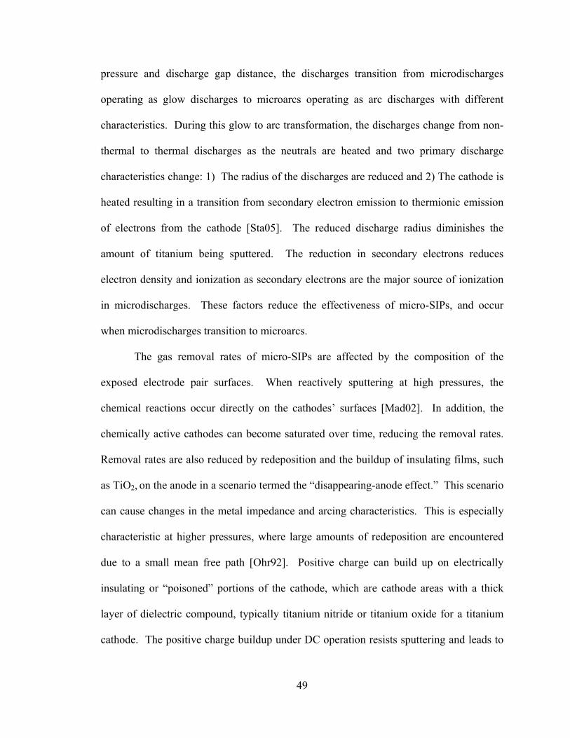
49
pressure and discharge gap distance, the discharges transition from microdischarges
operating as glow discharges to microarcs operating as arc discharges with different
characteristics. During this glow to arc transformation, the discharges change from non-
thermal to thermal discharges as the neutrals are heated and two primary discharge
characteristics change: 1) The radius of the discharges are reduced and 2) The cathode is
heated resulting in a transition from secondary electron emission to thermionic emission
of electrons from the cathode [Sta05]. The reduced discharge radius diminishes the
amount of titanium being sputtered. The reduction in secondary electrons reduces
electron density and ionization as secondary electrons are the major source of ionization
in microdischarges. These factors reduce the effectiveness of micro-SIPs, and occur
when microdischarges transition to microarcs.
The gas removal rates of micro-SIPs are affected by the composition of the
exposed electrode pair surfaces. When reactively sputtering at high pressures, the
chemical reactions occur directly on the cathodes’ surfaces [Mad02]. In addition, the
chemically active cathodes can become saturated over time, reducing the removal rates.
Removal rates are also reduced by redeposition and the buildup of insulating films, such
as TiO2, on the anode in a scenario termed the “disappearing-anode effect.” This scenario
can cause changes in the metal impedance and arcing characteristics. This is especially
characteristic at higher pressures, where large amounts of redeposition are encountered
due to a small mean free path [Ohr92]. Positive charge can build up on electrically
insulating or “poisoned” portions of the cathode, which are cathode areas with a thick
layer of dielectric compound, typically titanium nitride or titanium oxide for a titanium
cathode. The positive charge buildup under DC operation resists sputtering and leads to

50
arc formation [Mat03]. Magnetron sputtering targets use discrete pulses that allow the
targets to discharge any positive charge buildup on poisoned metal surfaces [Mat03], and
this technique can be applied to microdischarges as well. Additionally, very short pulses
of 10 ns have been shown to increase the electron density by a factor of 10 in
microdischarges as well as more than double the mean electron energy [Mos03].
Another method for potentially improving the gas removal rates of micro-SIPs is
to use heated cathodes to heat and impart energy to the ions directly above the cathode.
This will create more energetic microdischarges with higher energy collisions, translating
to higher energy ion impacts and improved “sputtering yield” (atoms sputtered/incident
atom). This in turn will improve micro-SIP efficiency. Heating the cathodes using thin-
film heaters differs from the heat induced by arc discharges as arc discharges heat
localized hotspots to a much greater extent than the thin-film heaters. The heat generated
by arc discharges cause the emission of thermionic electrons, while the heat generated by
the heaters does not to a significant extent. Without localized heating, modeled argon
microdischarges with similar currents to those used by micro-SIPs at 250 Torr heat the
gas temperature in the discharge by 58ºC over ambient slightly outside of the sheath
[Kus05]. The thin-film heaters are designed to be heated to 205ºC over ambient, heating
the neutral gas and ions in close proximity to the cathode.
To predict the quantified gas removal rate of micro-SIPs, a model is reported here
based on macroscale reactive sputtering models. Berg et al. [Ber87, Ber88] and Li and
Hsieh [Li05] present a model which considers the pressure change in a macroscale
system as a function of target erosion, gas injection, reactive gas gettering at all surfaces,
etc. The model determines the fractional coverage of a metal target and substrate by a

51
compound film as they are sputtered by argon mixed with a reactive gas. The fractional
surface coverage θ indicates the fraction of sites on the target surface occupied by the
compound over the total number of target sites, while (1-θ) indicates the fraction of un-
reacted metal sites. The change in the number of sites occupied by the compound on the
target per unit time is expressed as
( )1 Nm m N
JSdN FA a A FS A adt e
α θ θ α θ= − − + , (2.11)
where F is the reactive gas flux, A is the target area, αm is the sticking coefficient of the
reactive gas molecules to the pure metal, a is the “stoichiometric number of compound
formation” (ratio of compound molecules/reactive molecules), J is the ion current
density, e is the unsigned charge of an electron, and SN is the sputtering yield of the
compound. The first term in equation 2.11 represents the reaction between the reactive
gas molecules and the fresh metal portion of the target. The second term represents the
reduction in compound fraction as a result of sputtering the compound off the metal. The
third term represents the reaction between the reactive gas molecule and fresh metal sites
which are uncovered when a compound molecule is sputtered [Yos88]. The reactive gas
flux is determined using a Maxwellian distribution of molecular velocities as
2p
B
pF
mk Tπ=
, (2.12)
where pp is the partial pressure of the reactive gas, m is the mass of the reactive gas
molecule, kB is the Boltzmann constant, and T is the temperature. In this model, all of
the absorbed reactive gas molecules are assumed to contribute to the formation of
compound molecules on the target surface.

52
The macroscale model developed by Berg et al. [Ber87, Ber88] describes reactive
sputtering systems with low reactive gas partial pressures and requires adaptation to
describe the high-pressure environments in which micro-SIPs are operated in this study.
The primary difference between the two models is due to the high impingement rate of
reactive gas molecules at high pressures, which impinge due to random motion without
sputtering. These molecules can form native oxide layers, or other compound layers,
covering the entire substrate surface. This leaves no fresh titanium to getter reactive
molecules without sputtering. Theoretically, this can be confirmed by finding the critical
pressure above which the target surface is completely covered by a compound. This
critical pressure is determined by equating the rate at which the compound is removed by
sputtering and the rate at which the compound is formed by reactive gas molecules
impinging on the fresh metal sites, and solving for the pressure. The compound removal
rate is the second term in equation 2.11 and the compound forming rate is the third term
in equation 2.11. If the pressure is below the critical pressure, the compound is removed
faster than it is formed (until a steady-state is reached as presented in the Berg model),
while if the pressure is higher, compound eventually covers the target surface. The
critical pressure is:
( )1/ 2
crit
2 BN
N
mk TS JAPe S aA
πα
⎛ ⎞⎛ ⎞= ⎜ ⎟⎜ ⎟⎜ ⎟⎝ ⎠⎝ ⎠. (2.13)
Using nitrogen as the reactive and sputtering gas, using a titanium cathode as the
target, assuming stoichiometric TiN as the compound, and using other parameters
determined from the micro-SIP design, the critical pressure is calculated as 1.98 Torr.
Given that micro-SIPs are operated at pressures much higher than this, the entire surface

53
is covered during normal operation. Considering the use of pure nitrogen as a reactive
gas and given that the entire surface is covered by TiN after the native oxide layer is
removed, the removal of nitrogen gas only results from sputtering TiN molecules to
expose fresh titanium atoms which will bond with the nitrogen. This indicates that the
first term in equation 2.11 is irrelevant and the third term is the only relevant term
indicating nitrogen removal from the environment and, consequently, pressure reduction.
However, the process is now limited by the sputtering rate as opposed to the gas
impingement rate, making the rate of nitrogen removal by the micro-SIPs (molecules/s)
simply
pump NJR S Ae
θ= . (2.14)
This does not need to consider the sticking coefficient as available sites will be filled
much faster than the rate at which they are uncovered. TiN is considered to be sputtered
as a molecule, as opposed to as titanium and nitrogen separately. As no fresh titanium is
being sputtered from the cathode onto other portions of the substrate, all of the evacuated
gas molecules are bound to the surface of the cathode, and not on other portions of the
substrate.
The pressure reduction resulting from the removal of nitrogen from air is
determined using the parameters below. By the ideal gas law, the change in pressure is
BN
k Tdp JS Adt V e
θ= − . (2.15)
Considering a micro-SIP with a 50-µm discharge gap and 1,500 V applied at a pressure
of 100 Torr, 1.49 x 10¹⁴ molecules per second are sputtered and absorbed while the

54
pressure changes by 68.6 mTorr/minute. The rate at which nitrogen impinges on fresh
titanium is
m NdN FS Adt
α θ= (2.16)
and is equal to 5.2 x 10¹⁹ molecules per second. This is almost five orders of magnitude
faster than the rate at which the surface is sputtered, indicating that the assumption of a
sputter rate limited equation is valid.
Several parameters are required to calculate the gas removal rate of micro-SIPs
using the above equations, including the stoichiometric number, the sticking coefficients,
the sputtering yields, the electric field strengths, and the current density. The
stoichiometric number used is 2, as two titanium atoms can bond with a single N2
molecule. The sticking coefficient of nitrogen molecules on pure titanium is 0.4 at 20ºC
and the sticking coefficient of N atoms on TiNx films is ~0.003 for nitrogen-rich TiN
films [Yok05]. The sputtering yields, which are the number of atoms or molecules
ejected from a target surface per incident ion, are calculated for nitrogen ions impinging
on fresh titanium and TiN according to previously derived equations [Ohr92]. In a
nitrogen DC discharge with higher current but lower current density, N2+ ions have
average energies of 100 eV in the sheath, at the cathode [Kum93]. Higher applied
voltages also decrease the number of collisions for ions in the sheath, causing a larger
number of high-energy ions [Pet93]. Using an impinging ion energy of 100 eV, the
sputtering yield of pure titanium is calculated as 0.14 while the combined yield of
titanium and nitrogen from TiN is 0.24. A large number of ions have significantly less
energy but are not considered in the calculation. The combined yield of titanium and
nitrogen from TiN is typically larger than that of titanium from pure titanium, while the

55
yield of just titanium from TiN is smaller than that of titanium from pure titanium
[Ran01]. Sputtering yields are typically very low at high pressures but are aided by the
very localized microdischarges in micro-SIPs.
To determine the electric field strengths, field orientations, and electric field lines
produced by the micro-SIP electrodes, COMSOL MULTIPHYSICS® finite element
analysis (FEA) is used. A micro-SIP with 50-µm discharge gaps and an applied voltage
of 1,500 V is examined. The analysis reveals uniform electric field strengths around the
circular discharge gaps as shown in Fig. 2.5. Examining a three-dimensional image
reveals an arc-like orientation of electric field lines, which indicates that the distance
between electrodes, as experienced by the bombarding ions, is longer than the minimum
planar discharge gap separation. The theoretical distance is approximately four times the
planar discharge gap spacing, and this increase in distance is included in the micro-SIP
model to more accurately describe the ion trajectories. The resulting predicted maximum
electric field strength for this particular micro-SIP is 7.25 x 10⁶ V/cm without the
presence of a discharge, which is higher than traditional plasmas due to the small gap
spacing. The creation of a discharge would increase the field strength at the cathode, in
the sheath region, above this predicted value.

56
Unit: V / cm
Cathode
Anode
6 x 10⁶
4 x 10⁶
2 x 10⁶
1 x 10⁶
Figure 2.5: Modeled electric field strengths normal to a version 2 micro-SIP surface at a height of 50 µm above the electrodes.
The current density experienced by the ions is estimated as [Zhu98]
1(1 )
p IJC A e γ
⎛ ⎞= ⎜ ⎟ +⎝ ⎠, (2.17)
where I is the discharge current, p is the pressure, and C is a correction factor. The ion
current density is the total discharge current, as the current is carried by ions through the
sheath to the cathode, over the discharge area. It is reduced by the secondary electrons as
their negative charge repels ions, lowering the current density. The pressure correction
factor (p/C) is included to account for the change in microdischarge current density with
pressure. A summary of calculated parameters for the described micro-SIP is displayed
in Table 2.1.

57
Table 2.1: Calculated parameters for a micro-SIP with 50-µm discharge gaps and 1,500 V applied at a pressure of 100 Torr.
Parameter Value First ionization coefficient α (cm-1) 761 Second ionization coefficient γ 2.47 x 10⁻⁷ Current densities (A/cm2) 3.4 x 10¹⁶ E/p (V/(cm x Torr)) 750 Sputtering rate and nitrogen consumed (molecules/s)
1.49 x 10¹⁴
Nitrogen removal rate (mTorr/min) 68.6
2.4 DESIGN AND FABRICATION
Micro-SIPs with different electrode designs are used to examine the effect of
electrode design on gas removal rates and device durability. To maintain controlled,
progressive sputtering for extended durations of time, the cathodes are made larger than
the anodes and designed to erode evenly along the discharge gap boundaries. FEA
confirms that the circular design provides a uniform electric field over a large boundary
of interaction between the micro-SIP anode/cathode pairs. In contrast, if any sharp
corners are present, the discharges form at these locations preferentially. Three different
micro-SIP designs for prolonged reactive sputtering are fabricated on separate chips, each
with a 1 cm2 footprint. Discharge gaps of 5-150 μm are designed and fabricated but
discharge gaps less than approximately 35 μm tend to short due to microscale conductive
coatings such as dust. The first micro-SIP design (version 1) has two single
anode/cathode pairs and uses separate lead connections for each electrode, providing
redundancy should one electrode be destroyed through the application of a large current
or a bad connection. This design explores the use of a separate anode for each
anode/cathode discharge gap and large cathodes. The second micro-SIP design (version
2) [Fig. 2.6(a)] has a single composite anode that operates with eight separate but

58
identical cathodes. As anodes are not significantly sputtered by the discharge, a common
lead to them is sufficient. Each cathode can be activated individually or shunted off-chip
with others. In this design, four times as much titanium is available for reactive
sputtering as compared to version 1. The third micro-SIP design (version 3) [Fig. 2.6(b)]
has a single anode and two cathodes. Each cathode has 15 discharge gaps, which
maximize the amount of potentially sputtered titanium but version 3 does not allow the
user as much control compared to the other versions. Versions 1, 2, and 3 micro-SIPs
have 5.06 mm2, 1.82 mm2, and 33 mm2 cathodes respectively and each provides a distinct
operating advantage as previously described.
Figure 2.6: (a) Version 2 chip with a single anode and eight cathodes. (b) Version 3 chip with a single anode and two cathodes, each having 15 discharge gaps. (c) Version 4 chip with high current density. (d) Version 5 chip with low current density.
In addition to the devices described above, additional version 2 micro-SIPs with
identical cathode areas of 1.82 mm2 and discharge gap spacing of 35 μm, 50 μm, 75 μm,
100 μm, and 150 μm are fabricated to evaluate the relationship between gas removal rate

59
and discharge gap spacing. Despite the larger gaps, at atmospheric pressure the
breakdown voltages of these micro-SIP electrode pairs is theoretically estimated to be
between 500 V and 1,200 V.
To examine the effect of varied current densities on gas removal rates, micro-SIPs
having both small and large discharge gap boundaries between electrodes are used. The
micro-SIP design (version 4) [Fig. 2.6(c)] has pointed electrodes to confine the
microdischarges and produce high current densities over the small cathode areas.
Another micro-SIP design (version 5) [Fig. 2.6(d)] has extended discharge gap
boundaries between electrodes, to disperse the microdischarges and reduce the current
densities. While the electrodes in version 4 micro-SIPs only have a small point at which
the discharge gap is minimized, the version 5 electrodes have discharge gap boundaries
4.6 mm in length. Both designs have minimum discharge gaps of 50 μm, to allow
performance comparisons to version 1-3 micro-SIPs with 50-μm discharge gaps. These
micro-SIPs are fabricated on chips with footprints of 25 mm2, one-quarter the size of the
chips with micro-SIPs designed for prolonged sputtering.
Micro-SIPs utilizing micro-heaters as cathodes are designed to increase the
temperature of the microdischarges and a schematic diagram of the electrodes is shown in
Fig. 2.4(b). Four micro-heaters, 50 µm in width, serve as the cathodes and when heated
through the application of 3 V, reach temperatures of 232°C. These micro-SIPs are
designed for rapid sputtering over short periods of time, due to the small volume of
titanium available at the cathodes. They are fabricated on identical chips to the version 4
and 5 micro-SIPs.

60
All micro-SIPs were fabricated with two masks to simplify processing. A Ti film
(1 µm thick) and a Au film (500 nm thick) were thermally evaporated onto #7740
PyrexTM glass wafers (500 µm thick) without removing the wafers from vacuum. The
contact pads were patterned on the gold layer using photolithography and etched using
Transene GE-8148 gold etchant, which does not etch titanium. The electrodes were then
patterned in the titanium layer using photolithography to produce the patterns shown in
Figs. 2.6(a)- (d). Figure 2.7 illustrates the packaged devices.
Figure 2.7: A commercial package after opening, with two commercial pressure sensors and three different micro-SIP versions.
2.5 EXPERIMENTAL AND MODELING RESULTS
2.5.1 Removing Air from Microelectronic Packages
Micro-SIPs were sealed in industry-standard packages and re-sealable packages
with pressure sensors and operated with externally applied voltages while the pressure
was monitored. Version 1-3 micro-SIPs were used. They were hermetically sealed in

61
metal flatpack packages, which are often used for power electronics, using solder
bonding. The sealing was performed at the University of Michigan. One package was a
3.3 x 4.3 cm2 (6.33 cm3) gold plated nickel package from HCC Aegis (Catalog # 0J7H2),
while the second was a 2.5 x 2.5 cm2 (2.2 cm3) steel package from Sinclair
Manufacturing Co. (Product # SQ 1000-250-12-10GC). Stainless steel lids were used to
seal the packages at 760 Torr. A third, re-sealable glass package, 2.5 cm in diameter (4
cm3), was used to test the micro-SIPs at initial pressures lower than atmosphere. The
initial package pressure was set by a two-stage rotary vane roughing pump (Oerlikon
Leybold Vacuum Trivac D 16B), accompanying pressure controller (MKS® 600 Series),
and external macroscale pressure transducer (MKS® Baratron® Capacitance Manometer
model #627B23TDC1B). A needle valve was used to seal the re-sealable package while
the micro-SIP(s) operated. Large tubing external to the package was used to avoid low
conductance. The pressure was measured by two piezoresistive pressure sensors
(Freescale MPXH6115A) for confirmation in the larger (6.33 cm3) package and by one in
the smaller (4 cm3) and re-sealable package (4 cm3). A multimeter and a computer
interface were used to record the pressure sensor output voltages at programmable
intervals while the current was also recorded.
The pressures in the packages were reduced through micro-SIP operation. Three
micro-SIPs were sealed in the 6.33 cm3 package at atmospheric pressure. In one test
demonstrating a typical amount of air removal, 15 discharges 10 minutes in duration were
applied to the micro-SIPs using four different electrode pairs, and the pressure was
reduced by 168 Torr from the sealing pressure, as shown in Fig. 2.8. The pressure
remained steady for periods of up to 10 hours between discharges, and the figure shows

62
that the pressure sensor correctly measured atmospheric pressure when the cavity was
opened for inspection. Figure 2.9 displays the same pressure reduction and absorbed
molecules as a function of the energy used for the discharges. The upper trend line
represents the pressure drops measured with the discharge off, when no energy was being
applied to the system. In the 2.2 cm3 package, the pressure was reduced by 126 Torr
through the application of extended discharges. The ambient temperatures in the
packages never increased more than 2.2ºC during micro-SIP operation, as measured by
the increase in package pressure due to heating of the ambient environment from the
microdischarges.
500
600
700
800
0 10 20 30 40 50 60 70
Pre
ssur
e (T
orr)
Time (hours)
Extended Discharges
Seal Deliberately Broken
Short Discharges
Figure 2.8: Pressure drop in a 6.33 cm3 package over time. Fifteen consecutive 10 minute discharges drop the pressure 168 Torr. The pressure remains stable over periods of 10 hours of micro-SIP inactivity and returns to atmospheric pressure when the package is opened.

63
Cumulative Energy (kJ)
Pre
ssur
e D
rop
(Tor
r)
0
20
40
60
80
100
120
140
160
0 10 20 30 40 50 60
Pressure Drop Measured When Arc is Off
Pressure Drop Measured When Arc is On
Cumulative Energy (kJ)
Molecules A
bsorbed (1019)
0
20
40
60
80
100
120
140
160
0 10 20 30 40 50 60
Pressure Drop Measured When Discharge is Off
Pressure Drop Measured When Discharge is On
Equivalent Volum
e Rem
oved N
ormalized to P
ackage Volume
0
1
2
3
0
0.05
0.1
0.15
0.2
Figure 2.9: Pressure drop, shown in Fig. 2.8, as a function of cumulative energy supplied to the discharge with an initial pressure of 760 Torr. The upper and lower trend lines, respectively, show the pressure readings when the discharge is interrupted (causing spikes as the pressure stabilizes without an increase in energy) and when the discharge remains on. The corresponding number of gas molecules removed at room temperature, and the fraction of the package volume evacuated, are noted on the second Y axis.
A micro-SIP was operated with an initial pressure of 31 Torr in a 4 cm3 package.
It reduced the pressure by 4 Torr in 30 minutes, at an average rate of 133 mTorr/min, as
shown in Fig. 2.10. Operating micro-SIPs at relatively low pressures (1-30 Torr) resulted
in large amount of sputter redeposition. Testing micro-SIP operation at pressures below
30 Torr is addressed in the following sub-section.
26
28
30
32
0 10 20 30 40 50 60Time (minutes)
Pre
ssur
e (T
orr)
Discharge Initiated
Discharge Terminated
Figure 2.10: Pressure drop in a 4.0 cm3 package over 30 minutes of micro-SIP operation, starting at an initial pressure of 31 Torr.

64
2.5.2 Pressure Reduction Behavior
The general behavior of the pressure change with time during the microdischarge
induced sputtering, an example of which is displayed in Fig. 2.10, requires explanation.
At the initiation of a DC microdischarge, the pressure in the sealed microscale cavities
typically rose due to the heating of the ambient environment. The heating was found to
raise the temperature by a maximum of 2.2ºC, by measuring the heat induced pressure
increase, although the gas and ion temperature in the microdischarges increased by
hundreds of degrees. As the compound was sputtered from the cathode, molecules were
removed from the environment and the pressure began decline, eventually surpassing the
initial pressure. Reactively sputtering for short periods, e.g. 10 minutes, resulted in
pressure rises for approximately 3 of the 10 minutes before falling sharply.
When the micro-SIPs were operated for long periods of time, they demonstrated
signs of saturation. For example, the initial discharge in Fig. 2.8 reduced the pressure at a
rate of 678 mTorr/min, while the extended discharge utilized at a later time reduced the
pressure at a rate of 27 mTorr/min. Additionally, shown in Fig. 2.10, the micro-SIPs
demonstrated saturation after operating for periods of time as short as 30 minutes. This
saturation was eventually evident in all examined micro-SIPs and at higher pressures (>
≈100 Torr) appeared to be caused by a lack of cathode material after a great deal was
sputtered off, and by saturation of the titanium in the cathode. At lower pressures, the
saturation appeared to be caused by saturation of the titanium in the cathode and by
buildup of insulating nitride and oxide films on the cathode. As the insulating films
continued to be formed and re-deposited at the surface, the fresh titanium capable of
chemisorbing additional gas was buried and became increasingly unreachable by the

65
impinging ions. Temporarily reversing the electrode bias or using AC driven discharges
could have circumvented these restraints but was not examined. As this saturation
occurred, the package leakage rate eventually surpassed the pumping rate, as shown in
Fig. 2.10, at which point the discharge was terminated. The packages were increasingly
susceptible to leakage at low pressures due to the pressure difference between the sealed
and external environments and the low gas density which were compromised by small
amounts of leakage.
The pressure continued to decline after microdischarge extinction due to two
factors. The first involved the return of the packaged gas temperature to the original
state, as the microdischarge did not continue to heat the environment. The second factor
involved continued chemisorption by exposed titanium sites which had not formed
compound at the time of discharge termination. This occurred to a greater extent at lower
pressures as demonstrated in Fig. 2.10. After discharge extinction, the pressure continued
to drop for up to 20 minutes and eventually stabilized, holding steady for hours between
discharges as if the leakage rate was significantly low. Otherwise leakage caused the
pressure to increase.
Discharges of different durations produced varied pressure responses. Reactively
sputtering for short periods, e.g. 10 minutes, caused the pressure to rise and subsequent
decline after the gas removal countered the heating effects. Reactively sputtering for
extended durations, e.g. hours, resulted in steady pressure drops after initial rises due to
temperature. To maintain discharges for hours, the applied voltages required increases
with time due to the effective increase in discharge gap spacing as the proximal cathode
regions were sputtered away.

66
The titanium regions of the cathodes were sputtered as intended, which was
apparent upon opening the cavities, as shown in Fig. 2.11. A film was also evident on the
substrates and anodes. Areas of the 1-μm-thick titanium were completely removed down
to the substrate in the intended manner. As the titanium was sputtered from the initial
discharge locations, the discharges occurred at different locations and thus sputtered the
cathodes uniformly on all sides of the anodes. This uniform removal led to the concentric
consumption of the cathodes over time. The anodes remained largely intact, showing no
indication of sputtering, although some delamination and damage could potentially occur
due to heating caused by localized hotspots and arcs.
Figure 2.11: Micro-SIP electrodes displaying remains of a cathode after reactive sputtering, illustrating areas of complete titanium sputtering.
The device lifetime was dependent on microdischarge current density, which was
a function of the applied voltage and pressure. Operating at 760 Torr with an applied
1,000 V, the micro-SIPs lasted on the order of an hour before significant titanium was
removed and the devices became inoperative. At this point other cathodes were used. At

67
pressures below 300 Torr with an applied 1,000 V, the devices lasted for days and could
potentially last longer at lower operating pressures.
2.5.3 Operating Micro-SIPs at Lower Pressures
Micro-SIP operation was examined at pressures as low as 1 Torr. Version 2
micro-SIPs were enclosed in a re-sealable glass package, 2.5 cm in diameter (4 cm3), and
operated with an applied voltage of 1,500 V. Freescale MPXM2102 pressure sensors,
which operate between 0.1 Torr and 760 Torr, were used. However when the packages
were sealed at lower pressures (1 Torr), they were compromised by leakage and
outgassing, precluding micro-SIP evaluation at these initial pressures.
2.5.4 Relationship between Discharge Gap Spacing, Pressure, and Air Removal Rate
To determine the relationship between the micro-SIPs’ gas removal rates, the
initial ambient pressure, and the discharge gap spacing, micro-SIPs with varied discharge
gaps were operated in air at different initial pressures. Version 2 micro-SIPs with
identical designs and 1.82 mm2 cathodes were used, having 35 μm, 50 μm, 75 μm, 100
μm, and 150 μm planar physical discharge gaps at pressures between 100 Torr and 725
Torr in a re-sealable glass package, 2.5 cm in diameter (4 cm3). At these pressures all of
the discharge gaps were much larger than the mean free path of gas molecules. The
initial pressures inside the package were set using the procedure described in Section
2.5.1.
The air removal rate varied as a function of pressure, discharge gap spacing, and
discharge characteristics. Figure 2.12 shows the experimental and theoretically
determined pressure reduction rates as a function of starting pressure, ps. The theoretical
rates were determined using the calculated removal rate of nitrogen in air. The

68
theoretical model exhibits the same dependence of gas removal rate on pressure, but
overestimates the removal rate of large discharge gap micro-SIPs and underestimates the
rate of smaller discharge gap micro-SIPs. In micro-SIPs with smaller discharge gaps, 35
μm and 50 μm, higher initial pressures resulted in faster gas removal rates as a result of
the increase in electron density, ionization, and secondary electron peak power at
increasing pressures. At each examined pressure, micro-SIPs with smaller discharge
gaps generally remove air faster than micro-SIPs with larger discharge gaps. This is
consistent with the larger ionization coefficients, resulting increase in ionization, and
resulting increase in secondary electron production associated with smaller discharge gap
micro-SIPs. A change in micro-SIP discharge characteristics, from glow microdischarges
to microarcs, was associated with a reduction in removal rate. As the starting pressure
was increased for the micro-SIPs with larger discharge gaps, 75 μm and larger, the
discharges became spatially confined and the discharges exhibited arcing characteristics.
This corresponded to a decrease in pressure reduction rates. This decrease caused the
maximum pressure reduction rate of these micro-SIPs to occur at pressures less than
atmosphere. The coinciding change in discharge characteristics and pressure reduction
rate suggests that a reduction in secondary electron production in the arc-like discharges
reduced the pumping rate.
The high and low current density micro-SIPs proved to be unusable for extended
durations of time. The very high localized current densities encountered in the version 4
micro-SIPs eroded the cathodes within 10 minutes at atmospheric pressure, making them
unusable for long term operation. The low current density version 5 micro-SIP deposited
the sputtered material between electrodes, shorting them together and halting gas removal

69
within 5 minutes of use. These results indicate that significantly increasing or decreasing
the current density does not improve micro-SIP performance over that achieved with
version 1-3 micro-SIPs.
Ps = Starting Pressure (Torr)
ΔP /
Δt (m
Torr
/ min
)
Molecules rem
oved / min (10
16)0
100
200
300
400
500
0 200 400 600 800
35μm discharge gap
50μm
75μm
100μm
150μm
Air Experimental
0
1
2
3
4
5
6
(a)
Ps = Starting Pressure (Torr)
ΔP /
Δt (m
Torr
/ min
)
Molecules rem
oved / min (10
16)0
100
200
300
400
500
0 200 400 600 8000
1
2
3
4
5
635μm discharge gap
50μm
75μm100μm
150μm
Air Theoretical
(b)
Figure 2.12: (a) Experimentally measured (over 20 min.) and (b) theoretically determined pressure reduction rates in air as a function of discharge gap spacing and pressure. The micro-SIPs have between 35 µm and 150 µm discharge gaps, are operated with 1,500 V, have initial pressures between 100 Torr and 725 Torr, and are operated in a 4 cm3 package.
2.5.5 Removal Rates of Various Gases
Figure 2.13 shows the species being ionized and excited in an air environment at
760 Torr, as identified by examining the spectrum produced by the discharge [Pea63,

70
Har69]. In this mixed gas environment, the strongest emissions were produced by Ti+,
O+, and N2+.
Wavelength (nm)
Inte
nsity
(a.u
.)
200 300 400 500 600 700 800 900
334.92 nm (Ti+)323.6 nm (Ti+)
501 nm (N2+)
307 nm (Ti+)
430 nm (O+)453 nm (Ti)
376 nm (O+)
0
250
500
750
1000
Figure 2.13: Spectrum of the micro-SIP electrode pair discharge in air indicating the dissociation of oxygen and ionization of titanium and nitrogen.
The gas selectivity of titanium micro-SIPs was examined by individually
introducing pure nitrogen, oxygen, and helium (as an inert reference) into a previously
evacuated package and measuring the removal rates at 200 Torr. The micro-SIPs were
enclosed in a re-sealable glass package, 2.5 cm in diameter (4 cm3). The gas
concentration was set by MKS® Mass-Flo® Series Mass Flow Controllers (Model #’s
1479A13CR1BM and 1479A21CR1BM), accompanying pressure controller (MKS® 600
Series), and external macroscale pressure transducer (MKS® Baratron® Capacitance
Manometer model #627B23TDC1B). The air initially in the package was removed by a
two-stage rotary vane roughing pump (Oerlikon Leybold Vacuum Trivac D 16B). A
needle valve was used to seal the re-sealable package while the micro-SIPs operated.
The version 2 micro-SIP design with 1.82 mm2 cathodes and 100 μm discharge gaps was
used.

71
Figure 2.14 illustrates the partial pressure reduction in each environment; oxygen
is removed faster than nitrogen, and helium is not noticeably removed. Helium is not
removed as it is an inert gas and does not bond with titanium. In macroscale getter ion
pumps, inert gases are implanted and retained using complex cathode geometries or
tantalum (Chapter 1, Section 1.2). While inert gases might temporarily be implanted,
they will later be released as they are not chemically bonded to titanium. Figure 2.14
indicates this as the helium pressure is initially reduced, followed by an increase.
Averaging three trials, oxygen is found to be removed at 11.5 Torr/hr, nitrogen at 3.4
Torr/hr, and air at 7.2 Torr/hr. These reduction rates are significantly higher than those
observed in macroscale SIPs. Oxygen is removed at over three times the rate of nitrogen,
which corresponds to the ratio of chemisorption rates of these gases on titanium at room
temperature [Hol59]. This suggests that in a mixed gas environment such as air, oxygen
will be removed more rapidly than nitrogen as well. This was experimentally confirmed,
as shown in Fig. 2.14.

72
Molecules R
emoved (10 18)
-1.55
-1.05
-0.55
-0.05
0.45
0 10 20 30 40 50 60 70 80 90-16
-12
-8
-4
0
4
Time (minutes)
Pres
sure
Cha
nge
(Tor
r)
PS = 200 Torr
Helium
Air (control)
NitrogenOxygen
Figure 2.14: Change in pressure in environments of pure oxygen, nitrogen, helium, and air. The micro-SIPs have 100 µm discharge gaps, are operated with 1,000 V, have initial pressures of 200 Torr, and are operated in a 4 cm3 package. This shows that the mixed gas air environment is removed at a rate between oxygen and nitrogen as expected, based on the different chemisorptions rates of the gases. Helium is not removed as it is an inert gas and does not bond with titanium.
2.5.6 Removal Rate of Water Vapor
The ability of micro-SIPs to remove water vapor was determined by introducing
water vapor into sealed packages and measuring the relative humidity drop during micro-
SIP operation with humidity sensors. A re-sealable glass package, 2.5 cm in diameter (4
cm3), was used to test the micro-SIPs. Humidity was introduced through an Ace Glass
7533 Midget Impinger Bubbler. The initial package pressure was set by a two-stage
rotary vane roughing pump (Oerlikon Leybold Vacuum Trivac D 16B), accompanying
pressure controller (MKS® 600 Series), and external macroscale pressure transducer
(MKS® Baratron® Capacitance Manometer model #627B23TDC1B). A needle valve was
used to seal the re-sealable package while the micro-SIP(s) operated. Honeywell
HIH4000 humidity sensors were used to monitor the humidity in the package. The set-up
is shown in Fig. 2.15.
73
Humidity Sensor
PC DAQ Software
Multimeters
Glass Package
Micro-SIPElectrical Feedthroughs
Pressure Sensor
Power Supply (Vp)
RB
H2O Source
Bubbler
Air
Pump
Rotameters with Needle Valves
Figure 2.15: Schematic of the glass package, micro-SIP, and external equipment used to introduce and measure humidity removal.
Figure 2.16 shows the typical relative humidity and pressure drops observed using
a version 2 micro-SIP with a 100 μm discharge gap at a starting pressure of 400 Torr.
For comparison, it also shows the relative humidity drop when the rotary vane roughing
pump was used to reduce the pressure by the same amount in the same package. A
micro-SIP reduced relative humidity by 4% while reducing the pressure by 10 Torr in 45
minutes. Using the mechanical pump to reduce the pressure by 10 Torr, starting from the
same initial pressure and relative humidity, reduced the relative humidity by only 0.1%.
Initially, the micro-SIP removed humidity much faster than the mechanical pump over
the same pressure drop, but this measurement was influenced by the temperature increase
while the discharge was on, which caused a lower relative humidity reading. After the
micro-SIP was turned off, the relative humidity rose and stabilized at a value lower than
that obtained simply by removing the air with the mechanical pump. This indicates that
micro-SIPs can operate effectively in the presence of water vapor and may offer an
advantage to mechanical pumps in the suppression of humidity.

74
0 20 40 60Time (minutes)
Pressure (Mechanical Pump)
Pressure (micro-SIP)
Humidity (micro-SIP)
Humidity (mechanical pump)
375
385
395
405
415
Pres
sure
(Tor
r)
Relative H
umidity (%
)
53
57
61
65
69
Discharge Terminated
Heating Transient Cooling Transient
Figure 2.16: Experimentally measured change in humidity using a micro-SIP. The micro-SIP has a 100 µm discharge gap, is operated with 1,000 V, has an initial pressure of 400 Torr, and is operated in a 4.0 cm3 glass package. A mechanical pump is used for comparison, starting at the same initial pressure and relative humidity. The micro-SIP removes more relative humidity than the mechanical pump when both reduced the pressure by 10 Torr. The heating and cooling transients are caused by the discharge induced heat from the micro-SIP. They are absent in the mechanical pump measurements due to the absence of a heat increase.
2.5.7 Pulsed Discharge Operation
To evaluate the removal rate improvements possible through the reduction of
positive charge buildup on compounds covering the cathodes [Mat03], and possible
energy efficiency improvements, pulsed discharges were applied to version 2 micro-SIPs
with 50 μm discharge gaps at an initial pressure of 400 Torr in the re-sealable glass
package, 2.5 cm in diameter (4 cm3). Figure 2.17(a) shows the removal rates obtained
when the current applied to the micro-SIPs was pulsed for periods between 25 ms and
500 ms, at a frequency of 1 Hz. The rate at which air was removed from the package was
directly related to the duration of this applied current. Micro-SIPs operated using DC
discharges removed air faster than pulsed discharges with duty cycles of 50% or less,
showing that pulsing compromises evacuation rates. Figure 2.17(b), however, compares

75
ΔP /Δ
t (m
Torr
/ min
)
DC0
100
200
300
400
0 200 400 600 800Pulse duration (ms)
μm discharge gaps Torr
cm3 package
(a)
μm discharge gaps Torr
cm3 package
0 100 200 300 400Pulse duration (ms)
Pul
sed
Ene
rgy
Req
uire
d to
Rem
ove
Gas
Nor
mal
ized
to D
C V
alue
0
0.5
1
(b)
Figure 2.17: Pulses of 1,000 V are applied at a frequency of 1 Hz. (a) Pressure reduction rate as a function of pulse duration, averaged over 20 minutes of gas removal. The longer pulse durations reduce pressure faster. The error bars indicate a standard deviation of removal rate. (b) Relative energy required to remove an arbitrary unit of pressure with different pulse durations, normalized to a DC discharge. Pulses are five times more energy efficient, but require a longer duration of time.
the relative energy required by micro-SIPs using pulsed discharges of different durations
to remove a fixed amount of air from a package. The energy required to remove this
arbitrary amount of air with the different duration discharges is normalized to the amount
of energy required by a DC discharge. This indicates that given the same amount of
energy and enough time to apply this energy to pulsed discharges at a set frequency,

76
micro-SIPs using pulses of 25 ms in duration can remove almost five times as much air
as micro-SIPs using DC discharges. This also indicates that shorter pulses are more
energy efficient despite their slower removal rates as they are able to dissipate charge
buildup on the electrodes. Pulsed discharges have also been shown to increased electrode
lifetime as a result of shorter sputtering periods.
2.5.8 Thermally Assisted Discharges
To thermally assist the plasma and reactive sputtering, thin-film resistive heaters
were designed to serve as titanium cathodes for some micro-SIPs as shown in Fig. 2.4(b),
on Pyrex® substrates. These micro-SIPs were tested in the re-sealable glass package, 2.5
cm in diameter (4 cm3) using the procedure described in Section 2.5.1. Four heaters, 50
μm in width, 1 μm in thickness, and 1 mm or 2 mm in length, were heated by applying a
DC voltage drop of 3 V across them. The heaters had final calculated temperatures
increases between 218°C and 232°C. These temperatures were calculated using the
resistance of the heaters, the glass substrate thermal resistance, the applied voltage, and
the temperature coefficient of resistivity (TCR) of the titanium heaters. When the heaters
were turned on, they caused the temperature of the gas inside the cavity away from the
discharges to rise between 15°C and 19°C. This was measured by recording the
temperature induced pressure increase when the heaters were operated before micro-SIP
operation. For comparison, the temperature was raised by a maximum of 2.2ºC during
micro-SIP operation without heaters as cathodes. Identical micro-SIPs with inactive
heaters as cathodes were examined for comparison; the results, comparing the removal
rates of heated and unheated micro-SIPs at 100 Torr and 200 Torr, are shown in Fig.
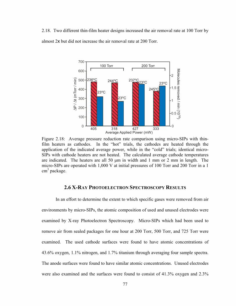
77
2.18. Two different thin-film heater designs increased the air removal rate at 100 Torr by
almost 2x but did not increase the air removal rate at 200 Torr.
Average Applied Power (mW)
ΔP /
Δt (m
Torr
/ min
)
Molecules rem
oved / min (10
16)
0
100
200
300
400
500
600100 Torr 200 Torr
0
0.5
1
1.5
23oC23oC
23oC 23oC236oC 244oC 237oC
245oC
405 318 427 333
700
2
Figure 2.18: Average pressure reduction rate comparison using micro-SIPs with thin-film heaters as cathodes. In the “hot” trials, the cathodes are heated through the application of the indicated average power, while in the “cold” trials; identical micro-SIPs with cathode heaters are not heated. The calculated average cathode temperatures are indicated. The heaters are all 50 μm in width and 1 mm or 2 mm in length. The micro-SIPs are operated with 1,000 V at initial pressures of 100 Torr and 200 Torr in a 1 cm3 package.
2.6 X-RAY PHOTOELECTRON SPECTROSCOPY RESULTS
In an effort to determine the extent to which specific gases were removed from air
environments by micro-SIPs, the atomic composition of used and unused electrodes were
examined by X-ray Photoelectron Spectroscopy. Micro-SIPs which had been used to
remove air from sealed packages for one hour at 200 Torr, 500 Torr, and 725 Torr were
examined. The used cathode surfaces were found to have atomic concentrations of
43.6% oxygen, 1.1% nitrogen, and 1.7% titanium through averaging four sample spectra.
The anode surfaces were found to have similar atomic concentrations. Unused electrodes
were also examined and the surfaces were found to consist of 41.3% oxygen and 2.3%

78
titanium by averaging the composition of five sample spectra. The remaining
composition of all electrodes was found to be contaminant carbon and silicon from the
substrates. While nitrogen was found in used electrodes, it could not be detected in
unused electrodes. However, aside from this disparity, the measurable atomic
concentrations gave little indication as to micro-SIP operation due to the oxidation of
micro-SIP surfaces in air after sputtering had ceased. Additionally, the extent of
implantation could not be determined. These results were similar to the results obtained
by Li et al. [Li07] in which XPS samples of titanium films used to chemisorb oxygen
were examined. Li found that carbon and oxygen were present, and attributed the
measured film surface compositions to the layer of reactive molecules that covered the
titanium films when exposed to air. See Appendix 2 for a detailed setup description and
complete results.

79
CHAPTER 3
PRESSURE SENSING USING MICRODISCHARGES
This chapter discusses microdischarge-based pressure sensors, which operate by
measuring the change, with pressure, in the spatial current distribution of pulsed DC
microdischarges. These devices are well-suited for high temperature operation because
of the inherently high temperatures of the ions and electrons in the microdischarges. Two
sensor versions are described. The first type uses three-dimensional arrays of horizontal
bulk metal electrodes embedded in quartz substrates while sensors of the second type use
planar electrodes. Section 3.1 presents other high temperature pressure sensors and
compares them to these sensors. Section 3.2 presents the operation of the
microdischarge-based sensors in detail and a current pulse circuit model. Section 3.3
presents the fabrication processes and device designs. Section 3.4 presents the
experimental results from both sensor geometries while Section 3.5 discusses factors
influencing the sensor output.
3.1 BACKGROUND
Pressure sensors amenable to high temperatures have uses in numerous industrial
sectors, and have additionally been used in gas turbine engines, coal boilers, furnaces,
and machinery for oil/gas exploration. Macroscale fiber optic pressure sensors have been

80
developed, but microscale sensors are advantageous as they can be utilized in small
volume cavities. These include combustion chambers, intake manifolds, and exhaust
manifolds of internal combustion engines [Flo90, Moc91, Che04]. Their small size also
allows attachment to gas turbine engines [Pul02]. Additionally, they can be inserted
down boreholes in oil/gas exploration equipment [Stu82]. Some high temperature fiber
optic pressure sensors have been reduced in size to several feet in length, including a
fiber optic based sensor using cubic zirconia prisms which has an operating temperature
of up to 1,000ºC [Pen05]. However, further miniaturization of high temperature sensors
expands their use to new applications.
Micromachined pressure sensors capable of operating in high temperature
environments have been fabricated and operate as interferometers on the ends of fiber
optical cables, beginning in the late 1970’s and early 1980’s. Four types of
interferometers have been constructed with fiber optic components: Mach Zehnder,
Michelson, Sagnac, and Fabry-Perot. Fabry-Perot interferometers use an air gap as an
optically reflective cavity. Light waves are sent through a fiber optic cable to this cavity,
where pressure alters the cavity’s size. This causes the reflected reference and sensing
light waves to interfere constructively or destructively, based on path length differences,
as they travel through the fiber optic to a sensing unit. This results in a measurable
change in Fabry-Perot reflectance peaks. Fabry-Perot interferometers, external to the
fiber optic cables, can use a thin-film diaphragm as a reflective surface at the end of the
cavity [Wol91, Wan05b] or two optical fibers with an air gap between them [Qi01].
Operating temperatures up to 800˚C have been achieved with sapphire membranes
[Fie04]. One Fabry-Perot sensor has been fabricated inside a fiber optic cable [Abe02].

81
To increase the operating range of these sensors, silicon carbide has been proposed as a
diaphragm material with sapphire optics [Pul02].
Another sensing technology uses Bragg gratings, which are photo inscribed into
fibers, and used to trace wavelength shifts caused by pressure and temperature changes
[Qia01, Zha02]. They can use light-emitting diode (LED) sources and trace reflected
wavelength shifts, caused by environmental changes, using spectrometers. These sensors
can be used to measure temperature and pressure simultaneously in oil and gas pipelines.
They have been used to measure pressure at 350˚C [Li07b]. Piezoresisitve pressure
sensors with diaphragms made from silicon carbide [Ned98], and more recently even
silicon [Guo08], have been reported to operate at 600ºC. Sapphire membranes have also
been used in this context [Fri06].
Microdischarge-based pressure sensors present another method for high
temperature pressure monitoring. These pressure sensors operate by measuring the
change in spatial current distribution of microdischarges with pressure. The targeted
pressure and temperature ranges are 10-2,000 Torr and 200-1,000˚C, as might be
encountered in a variety of manufacturing applications. As gas pressure increases, the
mean free path of ionized molecules is reduced and consequently, the breakdown and
discharge characteristics are altered. Microdischarge-based pressure sensors are
fundamentally different than ion gauges, which are not effective at atmospheric pressure
because the small mean free path of the created ions, 20-65 nm, makes them difficult to
detect at the collector [Ede90]. See Appendix 3 for a detailed discussion of the feasibility
and limiting factors in developing microscale ion gauges.

82
Two metrics of importance for high temperature, micromachined pressure sensors
are the temperature operating ranges and the fabrication complexity of the sensors. All
micromachined harsh environment sensors have the advantage of smaller footprints and
sizes compared to macroscale sensors, but can be further differentiated using these
metrics. The various high temperature microfabricated sensors are compared in Fig. 3.1,
showing the sensors’ operating ranges and fabrication steps required for construction.
The number of fabrication steps does not include packaging the sensor, and considers the
deposition and patterning of one layer as a single step. The devices using interferometers
external to the fiber optical cable were not tested at high temperatures but can potentially
operate at them. The temperature range of sensors utilizing fiber optics is also often
limited by the temperature range of the adhesives which attach the sensors to the fiber
optical cables [Wol91, Kim95]. Piezoresistive sensors can operate at high temperatures,
but require numerous fabrication steps. Microdischarge-based sensors are advantageous
in regards to these metrics as they provide fabrication and structural simplicity, requiring
as few as a single fabrication step, and the ability to operate at temperatures of 1,000˚C.
Microdischarge-based sensors offer several additional benefits. They utilize a
simple structure without moving components, which increases durability. Additionally,
they offer a direct electrical readout that simplifies packaging, unlike fiber optic based
sensors which require a fiber optic cable and package feedthrough. Finally, the presented
sensors benefit from a lack of complex and expensive electronics.

83
μD Planar
0
200
400
600
800
1000
0 1 2 3 4 5 6 7
P2
P3
EFP2
IFP
BG2BG1
EFP3
Fabrication Steps (#)
Max
imum
Ope
ratin
g Te
mpe
ratu
re (o C
)
EFP1
Bulk
P1
8 9
BG3
Microdischarge Range
Piezoresistive Range
Bragg Grating Range
Fabry-Perot Range
Symbol Type Ref EFP1 External Fabry-
Perot [Qi01]
EFP2 External Fabry-Perot
[Fie04]
EFP3 External Fabry-Perot
[Wan05b]
IFP Internal Fabry-Perot
[Abe02]
BG1 Bragg Gratings [Qia01]
BG2 Bragg Gratings [Zha02]
BG3 Bragg Gratings [Li07b]
P1 Piezoresistive [Ned98]
P2 Piezoresistive [Fri06]
P3 Piezoresistive [Guo08]
µD Bulk
Microdischarge Based
This work
µD Planar
Microdischarge Based
This work
Figure 3.1: Plot of maximum operating temperature vs. fabrication steps for various high temperature pressure sensors. (See table for the list of abbreviations and references.)
3.2 DEVICE CONCEPT AND OPERATION
Devices utilizing microdischarges are well suited for high temperature operation
as the bulk electrons have average thermal energies exceeding 3 eV (34,815 K) [Kus05,
Mit08c] away from the cathode and small populations of very high energy beam
electrons with thermal energies exceeding 400 eV near the cathode [Wil03a]. Ions have
thermal energies exceeding 0.03 eV (621 K) in a 23ºC (296 K) ambient environment.
These temperatures allow the species to be only minimally affected by a high or low
temperature ambient, making it possible for microdischarge-based devices to operate at
temperatures in excess of 1,000˚C and potentially down to cryogenic temperatures. The
targeted performance range for this work is 200-1,000˚C, but some baseline studies at
room temperature are included.

84
Two microdischarge-based microscale pressure sensor geometries are evaluated –
the Bulk Foil, and the Planar. Both geometries use multiple cathodes and provide a
differential current readout. (Multiple anodes may also be used; however, anode current
shows excessive pressure dependence because of the high mobility of electrons that
dominate it [Wil03a]. This high sensitivity results in relatively small dynamic ranges,
thereby limiting the utility of multi-anode configurations.) The first geometry, Bulk Foil,
uses bulk metal foils in a stress-relieved two-cathode stack within a quartz substrate, and
the second, Planar, uses planar thin-film metal electrodes on a Pyrex® substrate. The
Bulk Foil sensors are designed for very high temperature operation while the Planar
sensors, which use thin-film metals, are designed for conventional microfabrication.
While this effort focuses on the performance of these devices in a nitrogen ambient, with
appropriate encapsulation, they may be used in corrosive or liquid ambients.
The Bulk Foil sensor structure consists of several electrodes suspended over a
cavity in a quartz chip (Fig. 3.2). Each electrode has a single lead for electrical contact
and between one and three additional supports, which maintain the suspended position of
the electrode. A microdischarge chamber exists in the center of the chip, in a through-
hole, as shown in Fig. 3.2(a). A single disk-shaped anode electrode serves as the bottom
of the chamber while the center electrode is torus-shaped, allowing the discharges to exist
between the bottom anode and both cathodes. The top cathode is disk-shaped as well,
confining the discharges. The Planar sensor structure consists of several patterned
electrodes on the substrate. A single circular planar anode is partially surrounded by
concentric, C-shaped cathodes, and microdischarges are created above the electrodes as
shown schematically in Fig. 3.2(b).

85
(a)
(b)
Figure 3.2: Schematic of (a) a Bulk Foil sensor with electrodes above a quartz chip, illustrating placement, and the microdischarge chamber during operation, and (b) a Planar sensor with microdischarge.
To determine the pressure, it is first necessary to separately determine the current
in two of the cathodes. These current components are denoted as I1 in the proximal
cathode (cathode 1) and I2 in the distal cathode (cathode 2). The differential current,
expressed as a fraction of the total peak current, (I1 – I2) / (I1 + I2), is treated as the sensor
output. At low pressures, current favors the farthest cathodes, while at high pressures, the
opposite occurs. An important benefit of using a differential output that is expressed as a
fraction of the total is that the exact magnitudes are less important than fractional changes
or discharge size.

86
The basic operation of a DC microdischarge in a Bulk Foil sensor is illustrated in
Fig. 3.3, indicating electron and ion transport. The electrons are drawn towards the
anode, whereas the positive ions are drawn to the two separate cathodes forming
positively charged sheaths around them. Upon cathode impact, the energetic ions eject
high energy secondary electrons from the cathodes, which sustain the microdischarges by
ionizing additional neutral molecules and continuing the breakdown process. High
energy ions are encountered in microdischarges at pressures higher than atmosphere as a
result of the high power densities and voltage gradients encountered in the small gap
spacing. The current in each cathode is composed of a combination of positive ions
impacting the cathodes from the microdischarge and secondary electrons ejected from the
cathodes upon ion impact. Further away from the cathodes, the current is carried
primarily by the faster moving electrons.
Cathode 2
AnodeHigh Voltage Pulses
Cathode 1 Cathode 1Confined Microdicharge
e-
e-e-
e-
e-
e-
e-
e-
e-N2
+
O2+
O2+
N2+
N2+
N2+
N2+
N2
N2
O2
N2O2
N2
N2
I1
I2Positive Ions
Electrons
Neutral Molecules
e-
e- e-
e-e-
Secondary Electrons
Figure 3.3: Diagram of a microdischarge between a single anode and two cathodes in a Bulk Foil structure.
3.2.1 Pulsed Discharges
Power consumption and parasitic heating in the pressure sensors are controlled by
using pulsed DC microdischarges, as opposed to constant DC discharges. The use of

87
pulsed powering creates high current pulse arcs (40-100 ns in duration), which initiate the
microdischarges as described by several authors [Sta05, Rah07, Cho08]. The current
pulses are measured for operation as they provide greater sensitivity to pressure than the
sustained DC current levels in the microdischarges. It will be shown in Section 3.4 that
the magnitudes of the current pulses respond to pressure with greater sensitivity at low
pressures than at high, and that this characteristic also appears in the differential output of
the sensors. While steady state models exist for plasmas, the initial transient current
pulses encountered during microdischarge initiation have not been modeled.
Furthermore, the developed closed form microdischarge models are not viable for
complex arrangements in which there are more than two electrodes. The steady state
operating parameters of the microdischarges in a pressure sensor are presented in
Appendix 1.
3.2.2 Current Pulse Operation and Simulation
The current pulses in cathodes 1 and 2 of microdischarge-based pressure sensors
are roughly approximated by a circuit model, which predicts the pulse profile in time as a
function of discharge voltage. The pulse power source is represented by the discharging
of a capacitor, C, while the current pulse is represented as a series combination of an
inductance, L, and resistance, R, as developed by Robiscoe et al. [Rob88a, Rob88b]. A
large shunt resistance, Rs, is used to allow secondary current, Is, to drain the capacitor,
even if the pulse current, I, is zero. The pulse circuit model is shown in Fig. 3.4. As all
of the circuit elements are passive, the relationships between voltage drops across the
circuit elements result in a linear system of differential equations with constant

88
coefficients. The solutions to these systems are damped trigonometric oscillations if the
circuit rings, or exponentially decaying voltage profiles if the circuit is overdamped.
t = 0
C
RS
L
R
IS
I
V(t)
Pulsed Arc
Figure 3.4: Circuit model for discharge. The pulse power source is represented by the discharging of the capacitor, C, that is switched on at time t = 0. The current pulse is represented as a series combination of an inductance, L, and resistance, R along the current path. Rs is a shunt resistance, which allows a small amount of secondary current to flow during the main current pulse.
The circuit elements in the model can be determined using experimentally
obtained pulse values. The pulse rise time, pulse duration, peak current, and pulse energy
are all functions of the circuit element values, and can thus be used to determine these
values for the particular pulses encountered in cathodes 1 and 2 of the microdischarge-
based pressure sensors. The pulse rise time is expressed as
( ) 11 2 lnrLt rR
εε
⎛ ⎞= + −⎜ ⎟⎝ ⎠
, (3.1)
where ε = L/(CR2) and r = R/Rs. The pulse duration is expressed as
( ) ( )1 1pt RC rε= + −⎡ ⎤⎣ ⎦ . (3.2)
The pulse peak current is
0 11 lnVIp rR e
εε
⎡ ⎤⎛ ⎞= − −⎜ ⎟⎢ ⎥⎝ ⎠⎣ ⎦, (3.3)

89
where Vo is the initial applied voltage. The pulse energy is
( )( )2 /1
2 1 1oCV RQ
r rε=
+ +. (3.4)
100 1500 50 200
0
200
100
300
Cur
rent
(mA
)
M2
Time (ns) (a)
Time (ns)100 1500 50 200
0
200
100
300
Cur
rent
(mA
)
I2
(b)
Figure 3.5: Modeled (a) and experimentally measured (b) current pulses in cathodes 1 and 2 in a pressure sensor with electrodes spaced 50 µm apart, 1 mm in diameter, and 125 µm thick at 200 Torr. The modeled pulses are referred to as M1 and M2.
Figure 3.5(a) shows the theoretical current pulses in cathodes 1 and 2 of a
pressure sensor with electrodes spaced 50 µm apart, 1 mm in diameter, and 125 µm thick
at a pressure of 200 Torr. For cathode 1, the pulse rise time is 10 ns, the pulse duration,
measured from initiation to the Ip/e time, is 50 ns, and the peak current is 235 mA. For

90
cathode 2, the parameters are 20 ns, 40 ns, and 10.6 mA respectively. Using these
parameters and equations 3.1-3.3, the values for R, L, and C are obtained numerically for
each cathode. Further refinement is possible by fitting to experimental results. The
circuit elements for cathode 1 in the described sensor are found to be 2.6 kΩ, 25 µH, and
6.8 pF respectively and 48 kΩ, 600 µH, and 0.6 pF for cathode 2. The shunt resistance is
simulated as a large impedance, 100 kΩ. The predicted current pulses as a function of
time are determined through modeling utilizing SPICE. Similar analysis can be applied
to determine the circuit elements for various pressure sensor configurations.
In addition to the physical effects discussed above, it is worthwhile to consider
other possible contributors to the electrode current. Thermionic emission current, for
example, can be estimated by the Richardson-Dushman equation [Smi70]. This current
component is estimated to contribute at least four orders of magnitude less current than
the discharge current at 1,000˚C, although cathode spots could result in much higher
localized temperatures. The flow of electrons from field emission is considered
according to the Fowler-Nordheim equation. To contribute measurable current, the
electric field strengths need to be on the order of 107 V/cm [Cob58]. The maximum field
strength is predicted as 2.4 x 10⁵ V/cm utilizing COMSOL Multiphysics®, although this
considers a uniform electric field and the actual field strength may be much greater,
especially in the sheath. Additionally, unwanted asperities can concentrate and increase
electric field strength. These contributions are discussed in more detail in Appendix 1,
Section A1.5.

91
3.3 DESIGN AND FABRICATION
The Bulk Foil sensors, which are intended for operation at temperatures up to
1,000ºC, use a quartz substrate. For the electrodes, #302 stainless steel is used for several
reasons. Primarily, it is robust, inexpensive, easily machinable by micro-electro-
discharge machining (µ-EDM) [Tak02, Tak04, Tak06, Ric08] and photochemical
etching, and has a sufficient secondary emission coefficient (i.e. 0.04 secondary electrons
per incident 50 eV Na+ ion [Wal99]). Additionally, it is oxidation-resistant at high
temperatures and can be heated to 1,420ºC before melting. Alternate refractory metals
such as tungsten, molybdenum, and niobium oxidize at high temperatures in air, making
them less desirable. Platinum, iridium, and platinum-rhodium are attractive options but
are significantly more expensive than stainless steel.
The electrodes are lithographically patterned and etched from stainless steel foil,
using photochemical machining (Fig. 3.6) [All03]. This process involves coating a thin
sheet of metal with photoresist, exposing the resist, and spraying the sheet with a
chemical etchant to dissolve the exposed metal. The exposed metal is completely
removed, leaving through-holes in the sheet, and the resist is stripped (Fotofab, Chicago
IL). Alternatively, electrodes have been fabricated using micro-electro-discharge
machining.
Next, the electrodes are integrated into the substrate. An arrangement that
accommodates the expansion mismatch between electrodes and substrate is necessary.
Trenches of specified depths and a through-hole in the center are cut into the planar
quartz substrate. Both mechanical and wet-etch processes can be used for this purpose.
The electrodes are assembled into the trenches, with the circular portions located in the

92
through-hole. The different depths between the various trenches specify the discharge
gap spacing, as the electrodes lie flush with the bottom of the trenches. Ceramic epoxy
holds the electrode lead and support arms in place, without adhering to the stainless steel.
This allows the leads and supports to expand separately from the quartz chip and the
ceramic epoxy without buckling. High temperature-compatible wires are soldered to the
electrodes and the solder is encased in ceramic. This ceramic keeps the solder in position
so it maintains electrical contact, even at high temperatures.
1. Evaporate Ti and Au films onto Pyrex wafer.
2. Deposit and pattern photoresist.
3. Etch Au contact pads and strip photoresist.
Anode Cathode 1 Cathode 2
4. Deposit and pattern photoresist.
5. Etch Ti sensors and strip photoresist.
AnodeCathode 1
Cathode 2
Epoxy
6. Secure electrodes using high temperature ceramic epoxy, allowing expansion.
5. Insert electrodes into larger trenches, leaving room for metal expansion.
1. Deposit and pattern photoresist on stainless steel.
2. Spray etchant from both sides.
3. Strip photoresist and release electrodes.
Anode
Cathode 1
Cathode 2
4. Perforate and groove quartz substrate.
Bulk Sensor: Planar Sensor:
Figure 3.6: Fabrication processes for Bulk and Planar sensors.
The Planar sensors, which are intended for operation at temperatures up to 200ºC,
are even easier to fabricate (Fig. 3.6). The substrates are #7740 Pyrex® glass wafers,
which have a softening temperature of 820ºC. A Ti film (1 µm thick) and an Au film
(500 nm thick) are thermally evaporated onto 500 µm thick glass wafers without

93
removing the wafers from vacuum. Thin-film titanium electrodes are used as they have
previously been utilized to create sustained microdischarges [Wil01a]. The contact pads
are patterned on the gold layer using photolithography and the film is removed using
Transene GE-8148 gold etchant, which does not etch titanium. The electrodes are then
patterned in the titanium layer using photolithography.
Sensor characteristics such as the sensitivity, pressure dynamic range, and
temperature dynamic range depend on a variety of dimensional parameters, including
inter-electrode spacing, electrode diameter, and the cathode thickness. (Cathode
thickness effects sheath sizes as well as electrode spacing.) The anode/cathode spacing in
these sensors is set to produce measurable results up to 1,000ºC. (The sensors are
designed to function with an applied voltage of 1,000 V; altering the voltage results in
different sensitivities.) A typical Bulk Foil design with electrodes spaced 100 µm apart,
3 mm in diameter, and 50 µm thick is shown in Fig. 3.7(a). These sensors have active
areas of 7 mm2 and are fabricated on 4 cm2 chips. A typical Bulk Foil design with
electrodes spaced 50 µm apart, 1-2 mm in diameter, and 125 µm thick is shown in Fig.
3.7(b). These sensors have active areas of 0.8-3 mm2 and are fabricated on 1 cm2 chips.
The Planar sensors have 3-7 cathodes, of which two are selected for the pressure
measurement. The remaining are shunted to ground, and while they draw currents, they
are not used in pressure measurement. The cathodes are spaced 5-100 µm apart and are
5-300 µm in width. The sensors have active areas of 0.13-3 mm2 and are fabricated on
0.25 cm2 chips. A typical Planar sensor design, with three circular cathodes, spaced 50
µm apart and 300 µm in width, is shown in Fig. 3.7(c), while a design with five straight
cathodes spaced 50 µm apart and 50 µm in width, is shown in Fig. 3.7(d).

94
Figure 3.7: Bulk Foil sensors with (a) electrodes spaced 100 µm apart, 50 µm thick and (b) electrodes spaced 50 µm apart, 125 µm thick. Planar sensors with (c) three circular cathodes spaced 50 µm apart, 300 µm in width and (d) five straight cathodes spaced 50 µm apart, 50 µm in width.
3.4 EXPERIMENTAL RESULTS
Bulk Foil pressure sensors were fabricated and tested at various temperatures up
to 1,000ºC, measuring pressures between 10 Torr and 2,000 Torr. They were tested in a
vacuum chamber with the pressure set by a two-stage rotary vane roughing pump
(Oerlikon Leybold Vacuum Trivac D 16B) and accompanying pressure controller (MKS®
600 Series). Positive pressure was applied using compressed gas. The pressure sensors
were calibrated against an external macroscale pressure transducer (MKS® Baratron®
Capacitance Manometer model #627B23TDC1B). The temperature was set by testing
the sensors on a silicon nitride igniter (Igniters DirectTM Glo-stixTM), which was capable
of producing surface temperatures of 1,500ºC. The igniter consisted of a thin-film
tungsten heater insulated in planar silicon nitride structure. K-type thermocouples were

95
used to measure the temperature at the top and bottom surfaces of the pressure sensors at
several locations to provide a temperature control feedback system. Pulses, 1-20 ms in
duration, were applied at a rate of 2-10 Hz to the anodes of the sensors with positive
voltages between 700 V and 1,000 V. A computer controlled, single ended, transformer
coupled, gate drive circuit created the pulses (Fig. 3.8). A current limiting ballast resistor
was used in series with the anode, and 100-Ω resistors were used in series with each
cathode to measure current. The same circuitry powered Planar sensors. The pulses
consumed between 168 µJ and 6 mJ each.
Figure 3.8: Pulse generating and readout circuitry used for sensor operation.
The applied voltage pulses resulted in current pulses through each cathode as
shown in Fig. 3.9. The current pulses were approximately 40-100 ns in duration, with
amplitudes of 1.3 mA to 2.85 A in the Bulk Foil sensors and 25 mA to 2 A in the Planar
sensors, varying with temperature and pressure. The experimentally obtained pulses in
both cathodes are shown in Fig. 3.5(b). They demonstrated damped trigonometric
current oscillations.

96
Figure 3.9: Oscilloscope trace of the voltage pulses used for pressure measurements. The voltage was measured across 100 Ω resistors and used to calculate the current, with V1 as the voltage in cathode 1 and V2 as the voltage in cathode 2.
The sum of the measured cathode current pulse peaks for a Bulk Foil device is
presented in Fig. 3.10(a). At each temperature, this sum conforms to the equation:
Ipk1 + Ipk2 = C1 · ln(p) – C2 (3.5)
The terms C1 and C2, determined by a least-squares fit to the measured data in Fig.
3.10(a), are plotted in Fig. 3.10(b) as a function of temperature. At temperatures greater
than 600ºC, terms C1 and C2 saturate, indicating the total cathode peak current becomes
less dependent on temperature but remains dependent on pressure at higher operating
temperatures. The pressure in equation 3.5 was measured with the external macroscale
pressure transducer.

97
0
0.5
1
1.5
2
2.5
3
Tota
l Pea
k C
urre
nt (A
)
0 500 1000 1500 2000
Bulk Foil Sensor 50 μm spacing 1 mm dia. 125 μm thick
1000oC
400oC200oC23oC
Pressure (Torr) (a)
0
0.5
1
1.5
2
2.5
0 200 400 600 800 1000Temperature (oC)
Equ
atio
n Te
rms
(A)
C1
C2
Equation Terms for Peak Current
(b)
Figure 3.10: Measured current pulse peak values. (a) Sum of the pulse currents in two Bulk Foil cathodes as a function of pressure and temperature. The empirical curves for each temperature are indicated by the solid lines. (b) Temperature trend for equation terms C1 and C2 in the peak current equation.

98
0
20
40
60
80
100
0 500 1000 1500 2000Pressure (Torr)
Bulk Foil Sensor 50 μm spacing 1 mm dia. 125 μm thick
Cur
rent
in C
atho
de (%
)
Cathode 1 (I1)
Cathode 2 (I2)1000oC
Figure 3.11: Percentage of total current in the cathodes at 1,000˚C in a Bulk Foil sensor with electrodes spaced 50 µm apart, 1 mm in diameter, and 125 µm thick.
The Bulk Foil sensors were tested in a nitrogen filled chamber with temperature
and pressure control. Figure 3.11 shows fractional cathode currents, at 1,000˚C, for a
sensor design with electrodes that were spaced 50 µm apart, 1 mm in diameter, and 125
µm thick. As noted, the output of the sensor is the differential peak current between two
cathodes, expressed as a fraction of the total peak current. The typical output for this
sensor is shown in Fig. 3.12(a). Figure 3.12(b) presents the typical output from a sensor
design with electrodes spaced 100 µm apart, 1 mm in diameter, and 125 µm thick. The
sensors demonstrate two regions of sensitivity (similar in some sense to touch-mode
capacitive pressure sensors [Cho92]). At low pressures the response is highly linear,
whereas at high pressures it conforms to equation 3.5. The transition between these two
regions rises from about 100 Torr at room temperature to about 500 Torr at 1,000°C. The
average sensitivities in the low pressure and high pressure operating regions of these
sensors are shown in Fig. 3.13 as functions of temperature.

99
-0.2
0
0.2
0.4
0.6
0.8
1
0 500 1000 1500 2000Pressure (Torr)
Bulk Foil Sensor 50 μm spacing 1 mm dia. 125 μm thick S
enso
r Out
put (
I 1 - I
2) /
(I 1 +
I 2)
1000oC
400oC200oC23oC
(a)
-0.2
0
0.2
0.4
0.6
0.8
1
0 200 400 600 800 1000 1200
Pressure (Torr)
Sen
sor O
utpu
t (I 1
- I2)
/ (I 1
+ I 2)
Bulk Foil Sensor 100 μm spacing 1 mm dia. 125 μm thick
1000oC
400oC
200oC23oC
(b)
Figure 3.12: Differential current output determined from the percentage of total current in Bulk Foil sensors with electrodes (a) spaced 50 µm apart and (b) spaced 100 µm apart, 1 mm in diameter, and 125 µm thick. Each data point is the average of 100 measurements. The two empirical curves per temperature are indicated by the solid lines.
Sensitivity is measured in parts per million per Torr (ppm/Torr), in which the full-scale
sensor output is viewed as a million “parts”. The “parts per million” indicates the change
in the percentage of the full scale sensor output (change in parts/one million parts),
typically over a unit pressure for pressure sensitivity or over a unit temperature for
temperature sensitivity. For these sensors, the sensitivity is measured per Torr. The

100
0
1000
2000
3000
4000
5000
6000
0 200 400 600 800 1000
Sen
sitiv
ity (p
pm/T
orr)
Typical Sensitivity of Piezoresistive Sensors at Room Temperature
Typical Sensitivity of Capacitive Sensors at Room Temperature
Temperature (oC)
Bulk Foil Sensor 50 μm spacing 1 mm dia. 125 μm thick
Low Pressure Range Sensitivity
High Pressure Range Sensitivity
(a)
0
1000
2000
3000
4000
5000
6000
0 200 400 600 800 1000
Sen
sitiv
ity (p
pm/T
orr)
Typical Sensitivity of Piezoresistive Sensors at Room Temperature
Typical Sensitivity of Capacitive Sensors at Room Temperature
Temperature (oC)
Bulk Foil Sensor 100 μm spacing 1 mm dia. 125 μm thick
Low Pressure Range Sensitivity
High Pressure Range Sensitivity
(b)
Figure 3.13: The average sensitivities in both the low and high pressure ranges for the Bulk Foil sensors in Fig. 3.12(a) and (b) as functions of temperature.
temperature coefficient of sensitivity is a measure of the change in sensor output as a
function of temperature, and is measured in parts per million per kelvin. One sensor
design typically demonstrated the maximum lower pressure sensitivity, 5,420 ppm/Torr,
as well as the maximum higher pressure sensitivity, 500 ppm/Torr.

101
The use of three, or more, cathodes to simultaneously enhance both sensitivity
and dynamic range (albeit at the cost of increasing lead count at the circuit interface) was
explored. Devices with three or more cathodes were fabricated and the signal output of
two cathodes was used. The signal generated from two cathodes of a Bulk Foil sensor
that had three cathodes spaced 100 µm apart, 3 mm in diameter, and 50 µm thick,
provided a relatively high sensitivity of 5,000 ppm/Torr. Unfortunately the sensor had a
compromised dynamic range of only 300 Torr. Other design variations were also
explored and the typical results are listed in Table 3.1. The minimum average
temperature coefficient of sensitivity was -550 ppm/K.
Table 3.1: Typical performance of four different sensor designs with the highest performance in each category in bold.
Sensor Parameters
Max Low Pressure
Sensitivity (ppm/Torr)
Max High Pressure
Sensitivity (ppm/Torr)
Dynamic Range (Torr)
Temp. Coeff. of
Sensitivity (ppm/K)
Planar W=300 µm G =50 µm 9,800 1,400 175 -1,412
Bulk D=1 mm W=125 µm G=50 µm
5,060 380 2,000 -650
Bulk D=1 mm W=125 µm G=100 µm
2,170 220 1,150 -550
Bulk D=2 mm W=125 µm G=100 µm
5,420 500 900 -925
The Planar sensors were tested in the context of a chemical sensing system, with
an inert carrier gas (He) along with air and organic vapors (Chapter 4, Section 4.4).

102
Packaging these sensors with other devices and operating them concurrently
demonstrated the ability of microdischarge-based sensors to function in systems, without
disrupting the operation of other components. The helium, air, and organic vapors were
introduced into the microscale package with the pressure set by a two-stage rotary vane
roughing pump (Oerlikon Leybold Vacuum Trivac D 16B) and accompanying pressure
controller (MKS® 600 Series). The pressure measured by the Planar pressure sensors was
calibrated against an external macroscale pressure transducer (MKS® Baratron®
Capacitance Manometer model #627B23TDC1B). Figure 3.14(a) illustrates the
fractional cathode current and differential output of a Planar sensor packaged with other
devices as described above, with three cathodes spaced 50 µm apart, 300 µm in width. In
this geometry, the intermediate cathode was grounded. Typical sensitivity was 9,800
ppm/Torr in the lower pressures, from 30-100 Torr, and 1,400 ppm/Torr in the higher
pressures, from 100-200 Torr. Figure 3.14(b) illustrates the output of a Planar sensor
with five cathodes spaced 50 µm apart, 50 µm in width, which produced a uniform
sensitivity of 2,000 ppm/Torr across both pressure regions from 25-275 Torr at 23˚C
using cathodes 1 and 2. The remaining cathodes were grounded. The impact of Planar
electrode geometries was also investigated. Planar sensors with five cathodes spaced 5
µm apart and 5 µm in width, and 10 µm apart and 10 µm in width, were examined but
demonstrated low sensitivities, as did sensors with straight cathodes, as opposed to
circular. This indicates radial symmetry of the cathodes around a central anode is a
feature worth retaining.

103
I1-I2I1+I2
0.6
0
0.2
0.4
10050 150 200 2500
0.6
-0.2
0
0.2
0.4
Pressure (Torr)
Cur
rent
in C
atho
de (%
) Sensor O
utput (I1 - I2 ) / (I1 + I2 ) Anode
Cathodes1
2Dummy
Cathode 2 (I2)
Cathode 1 (I1)
200oC Planar Sensor 50 μm spacing 300 μm wide
Cathode 1 (I1)Cathode 2 (I2)I1-I2I1+I2
(a)
0
0.1
0.2
0.3
0.4
0.5
0.6
0
0.1
0.2
0.3
0.4
0.5
0.6
0 100 200 300Pressure (Torr)
12
Anode
CathodesDummies
I1-I2I1+I2
Sensor O
utput (I1 - I2 ) / (I1 + I2 )
Cur
rent
in C
atho
de (%
)
Cathode 1 (I1)
Cathode 2 (I2) Planar Sensor 50 μm spacing 50 μm wide
(b) Figure 3.14: Percentage of total current and differential current output in Planar sensors with (a) electrodes spaced 50 µm apart, 300 µm in width and (b) electrodes spaced 50 µm apart, 50 µm in width. Each data point is the average of 100 measurements.
Sensitivity, dynamic range, and the temperature coefficient of sensitivity are
metrics used to compare microdischarge-based pressure sensor designs to one another
and other pressure sensors. The performance of four different sensor designs, both Planar
and Bulk Foil, are shown in Table 3.1, with the highest performance in each category in
bold. The data in the table represents typical operation of each sensor design.

104
3.5 DISCUSSION OF RESULTS
Several points concerning the sensor operation warrant a discussion, the
temperature coefficients of sensitivity, the potential impact of electrode contamination,
and the possibility of encapsulation.
The sensors demonstrate a negative temperature coefficient of sensitivity. For
example, a sensor with electrodes spaced 50 µm apart, 1 mm in diameter, and 125 µm
thick has a sensitivity in the low pressure region of 5,060 ppm/Torr at 23ºC and 1,420
ppm/Torr at 1,000ºC. There are a number of possible contributors to the temperature
coefficient of sensitivity, ranging from changes in the nature of the microdischarge to
structural effects such as minor variations in electrode separation caused by expansion
mismatch with the substrate. For comparison, typical piezoresistive and capacitive
pressure sensors have sensitivities of 100-1,000 ppm/Torr respectively, and temperature
coefficients of sensitivity of ±1,000 ppm/K to ±5,000 ppm/K [Zha94, Hak06].
In nitrogen environments, coating of the electrode surfaces with contaminating
thin films is not a primary concern, in these sensors. In the past, microdischarges have
been used to, and can unintentionally, coat electrode surfaces in reactive environments
[Sch05]. However, with discharges of sufficient energy, thin films are sputtered off the
electrodes. This is demonstrated through the successful use of titanium electrodes, which
form native titanium oxide layers in air. Radio frequency discharges are also utilized to
remove coatings [Riz77].
In general, microdischarge-based pressure sensors should be calibrated for the gas
environment in which they operate. To permit operation in variable environments that
may additionally contain corrosive gases or even liquids, the pressure sensors can be

105
encapsulated within a sealed cavity with a flexible diaphragm. The sealed cavity could
contain pure nitrogen, helium, or other gas in which the discharges would be created.
The external fluidic pressure would be transferred to the encapsulated gas through the
diaphragm, taking advantage of the high sensitivity of the pressure sensors.

106
CHAPTER 4
CHEMICAL SENSING MICROSYSTEM
This chapter discusses the exploratory use of the microscale-sputter-ion pump and
microdischarge-based pressure sensor in a harsh environment microdischarge-based
chemical sensing microsystem at temperatures of up to 200ºC. In particular, the ability of
the micro-SIP to purify gas environments of contaminating gases is explored as it purifies
spectra for an optical emission sensor. This system has three microdischarge-based
devices in total: a pressure sensor, a gas purifier, and an optical emission sensor. The
system operates by obtaining a gas sample while monitoring the pressure, purifying the
sample using a micro-SIP, and determining the gases present in the sample using an
optical emission sensor. The ability of the system to purify samples for carbon detection
is discussed. Section 4.1 presents the need for harsh environment chemical sensors, a
comparison of currently used harsh environment sensors, and a comparison of
microdischarge-based optical emission sensors. Section 4.2 presents the need to remove
contaminant gases such as nitrogen when performing spectral chemical sensing by
illustrating the ability of nitrogen to preclude SF6 detection. Section 4.3 presents the
ability of micro-SIPs to purify gas environments from contaminating nitrogen and
oxygen. Section 4.4 presents the system for gas phase chemical detection in harsh
environments.

107
4.1 BACKGROUND
The detection of chemicals in harsh environments is important to numerous
industries and researchers. In particular, the use of microscale harsh environment
chemical sensors can potentially reduce the cost of drilling for petroleum exploration,
field development, and long-term geological monitoring [Alb00]. During petroleum
exploration and pumping, the flow of removed material is a combination of oil, water,
and gases. Continuous down-hole analysis of gas during petroleum pumping is useful for
the control of product quality, the detection of unwanted contaminants, and the
optimization of product treatment downstream [Hun97]. Continuous chemical analysis is
also useful during petroleum detection. The down-hole sensors for detection and
monitoring must be able to withstand elevated temperatures and pressures. They also
must be able to detect carbon, sulfur-containing gases, and contaminant gases such as
H2S and CO2 [Col95, Hun97]. Other high temperature applications also require chemical
sensing and monitoring. For example, automobile emission control requires monitoring
of the levels of nitric oxides (NOx) and hydrocarbons (CxHy). Two metrics of importance
to high temperature, micromachined gas sensors are the temperature operating ranges and
the number of chemicals detectable by the sensors. These metrics will be used to
evaluate different sensors and sensor technologies.
Numerous miniature high temperature chemical sensors have been developed.
Miniaturization of chemical sensors for portable applications often involves the
utilization of new technologies as many macroscale technologies cannot be scaled using
typical fabrication processes. Instead, many miniature sensors utilize the changing

108
properties of thin films in which target molecules are adsorbed on the surface of these
films and cause some property of the thin films to change. The selectivity of the sensors
is often tailored to the analyte(s) of interest by varying parameters including: dopants,
grain sizes, catalysts, external filters, operating temperature, and many other factors
[Wil01b].
There are three primary modes of operation of thin-film sensors. (1) Resistor type
sensors (chemiresistors) which exhibit linear IV curves that reversibly change as a
function of partial pressure of molecules. (2) Capacitor-type sensors based on
metal/oxide/semiconductor (MOS) devices which show voltage-dependent CV curves.
(3) Diode-type sensors which show partial-pressure-dependent non-linear IV and CV
curves. In addition, field effect transistors utilizing chemical sensitive gates, chemFETs,
acoustic wave technology including bulk and surface acoustic wave devices (BAW and
SAW), and ion mobility sensors have been also used.
Chemiresistors in their simplest form consist of a selective layer whose
conductivity is modulated by interaction with analyte(s). They are arguably the most
commercially successful miniature gas sensor and have the advantages of compact size,
simple fabrication, low cost, and simple measurement electronics [Wil01b, Jan03]. They
are commonly used to monitor oxidizing and reducing gases such as O2, H2, CO, NO2,
and hydrocarbons [Gop96] and have a detection limit range from ppb’s [Cai02] to a few
hundred ppm [Dav05] depending on the coating used. Chemiresistors typically monitor
one or several chemicals, but can be arranged in arrays to expand their analysis [Dom97].
Unfortunately, control of chemiresistors’ surface properties can be challenging,
especially when they are affected by usage conditions and temperature variations. In

109
addition, their sensitivity is highly dependent on the fabrication process and they can
require hours to recover when operated at temperatures less than 200ºC. They are also
hampered by signal-to-noise ratio limitations.
Several semi-conduction metal oxide (SMO) chemiresistors have been developed
for use at high temperatures. Metal–oxide chemical sensors have been used in both the
research and commercial communities because they can be fabricated at least as easily
and with greater stability than other chemiresistive materials, such as polymers and
organic films. Typical sensors use zirconium oxide, gallium oxide, or tungsten oxide
while niobium oxide has also been utilized [Che08]. Vapors that can be sensed
effectively include ammonia, hydrogen, hydrogen sulphide, ozone, propane, sulphur
dioxide, hexane, carbon monoxide, various saturated and unsaturated hydrocarbons, and
other reducing gases. A list of various semi-conduction metal oxide films used, vapors
sensed, temperature ranges, and benefits of the various films is presented by Wilson
[Wil01b]. The listed sensors use various metal-oxide films to detect between one and
five vapors and operate at temperatures of 250-1,000ºC. For example, gallium oxide
sensors have been fabricated which measure oxygen content from 600-1,000ºC [Fle91,
Hoe01, Ogi01]. Other metal-oxide chemical sensors can measure NO and NO2 [Hoe01,
Miu03].
Metal insulator semiconductor (MIS) or metal oxide semiconductor (MOS)
sensors measure capacitance changes with gas partial pressure. They are composed of a
gas sensitive metal, typically platinum, deposited on an oxide adherent to a
semiconductor. To operate at high temperatures, silicon carbide has been used instead of
silicon, forming metal-insulator-silicon carbide (MISiC) structures. Species that have

110
been monitored with MISiCs at high temperatures include hydrogen, hydrocarbons,
nitrogen oxides, and fluorine containing gases. Hydrogen and oxygen have been
measured at 400ºC [Tob03] and 30 ppb of fluorine has been detected at 350ºC [Vas98].
These devices have been operated up to 600ºC for short periods of time but stable long-
term operation is limited to a few days by measurand and temperature permanently
induced modifications to the materials [Thi06].
Schottky-barrier sensors measure a shift to a lower bias voltage in the presence of
certain gases. These devices originally used Pd:MOS structures, and later used
metal/insulator/silicon carbide diodes with Pt Schottky contacts. Nitrides have been used
as insulating layers for high temperature operation including gallium nitride, indium
nitride, aluminum nitride, and boron nitride. They have been used to detect hydrogen and
hydrogen containing gases at temperatures up to 600ºC as well as methane, ethylene, CO,
NO, NO2, butane, and propane [Kim01, Eic03]. However, extended operation at high
temperatures is compromised due to junction breakdown and electromigration [Thi06].
ChemFETs measure the change in work function of a thin-film metal or polymer
as a function of adsorbed vapor by using this thin film as a gate material in a field effect
transistor. They have been shown to operate at temperatures as low as ambient using
polymer films, but have previously been operated at temperatures of 200ºC [Cov04]. In
general, ChemFETs are capable of higher signal-to-noise ratios than chemiresistors but
are inherently more complex to fabricate and require more extensive control and
measurement electronics. These characteristics increase their cost and limit the number of
ChemFETs that can be placed inside a single device [Wil01b].
111
Surface acoustic wave sensors (SAW) measure the change in delay or resonant
frequency of a surface acoustic wave launched on the surface of a piezoelectric material
due to changes in the composition of the surrounding environment. They are one of the
most sensitive micromachined high temperature sensors. Most commonly quartz, lithium
niobate (LiNbO3), and lithium tantalate (LiTaO3) crystals are used as substrate materials.
A device utilizing langasite (LGS) crystals is able to operate at 750ºC, a higher obtainable
operating temperature than that of devices using common crystals, and can detect 1,000
ppm H2 and 10 ppm C2H4 [Thi06]. Devices capable of detecting 10 gases have been
developed [Fan99].
Ion mobility mass spectrometry (IMS) sensors separate and identify gas phase
ions based on their different mobilities. Ions are carried between parallel plate electrodes
by a flow of gas while RF and DC voltages cause the ions to follow trajectories
perpendicular to the flow. The mobilities of the ions become field dependent in these
conditions. An ion mobility spectrometer, capable of operating at atmospheric pressure,
has been miniaturized and used to distinguish several gases [Mil01, Eic03a].
Devices which measure changes in electrochemical properties of a solution, such
as ISFET’s [Jan03], potentiometric sensors [Nam03] and ampereometric sensors [Mar05]
have also been developed. These sensors have very low detection limits (in the ppb
range) but show large variation, as it is difficult to construct miniature reference
electrodes.
The microscale optical emission sensor presented in this chapter utilizes
microdischarges between thin-film electrodes. Microdischarges are used in a variety of
micro total analysis systems including microscale optical emission spectroscopy systems

112
for chemical sensing [Bro02, Fra03, Kar04]. These devices, based on microdischarge
and arc emissions, operate by exciting gas species and observing the characteristic
spectral output from the energy transitions [Bra68]. Similar devices developed by
Caviton, Inc. have been shown to operate at 1,100ºC during metal detection tests
[Cav07]. Since most atomic species produce emission lines, emission spectroscopy can
be used to identify numerous species concurrently while providing specificity as each
species has characteristic emission spectra. The detection is also rapid, requiring a few
milliseconds. Devices utilizing microdischarges are well suited for high temperature
operation as previously described in Chapter 3.
Various varieties of microfabricated sensors are compared in Fig. 4.1, showing
the sensors’ operating ranges and number of chemicals detectable by a single sensor of
each type. All of the sensors demonstrate high sensitivity in harsh environments, but
thin-film sensors focus on the detection of a single or several gases, as opposed to
detecting a majority of the gases present. To counter this, arrays of sensors having
different coatings are used instead of single sensors to expand the range and selectivity.
The complexity of the sensor readout circuitry and the fabrication process determines the
number of different devices on the array. It is assumed that although the sensors
themselves are non-specific, the overall signature is specific [Gar99]. This solution is
limited, as it is difficult to fabricate large arrays inexpensively. However, devices based
on optical emission spectroscopy from microdischarges operate faster than thin-film
devices and can detect a large number of specific chemicals concurrently, without the
added complexity of having multiple devices. Figure 4.2(a) compares the sensitivity
against the speed of detection for various types of chemical sensors and Fig. 4.2(b)

113
compares the selectivity against the number of detectable chemical species for gases and
organic compounds.
20
μD
0
200
400
600
800
1000
0 80 100Chemicals Detected (#)
Ope
ratin
g R
ange
(o C) CR2
CAP2CAP1
CR5
CR3
SB
FET
SAW1
SAW2
Chemiresistor
CapacitiveSchottky-barrier
ChemFET
SAW
MicrodischargeCR1CR4
IMS
IMS
Symbol Type Ref CR1 Chemiresistor [Fle91] CR2 Chemiresistor [Hoe01] CR3 Chemiresistor [Ogi01] CR4 Chemiresistor [Wil01b] CR5 Chemiresistor [Miu03] CAP1 Capacitive [Vas98] CAP2 Capacitive [Tob03] SB Schottky-barrier [Eic03] FET ChemFET [Cov04] SAW1 SAW [Fan99] SAW2 SAW [Thi06] IMS Ion Mobility [Mil01] µD Microdischarge
Based [Cav07] / This work
Figure 4.1: Plot of operating temperature range vs. number of detectable chemical species for various high temperature gas sensors. (See table for the list of abbreviations and references.)
Microdischarge-based sensors can also operate at both ambient and high
temperatures, while some of the discussed thin-film sensors cannot operate at low
ambient temperatures. In addition, most of the thin-film sensors have cross-sensitivities
to many different chemicals, which make false positives problematic. Another issue with
thin-film sensors is that the response, stability, and sensing properties of these films are
highly dependent on the fabrication process [Thi06]. This results in short sensor lifetime
or expensive calibration with numerous gases. Microdischarge-based optical emission
sensors do not suffer from these issues. Additionally, utilizing pulsed discharges, they
can operate for extended periods of time.
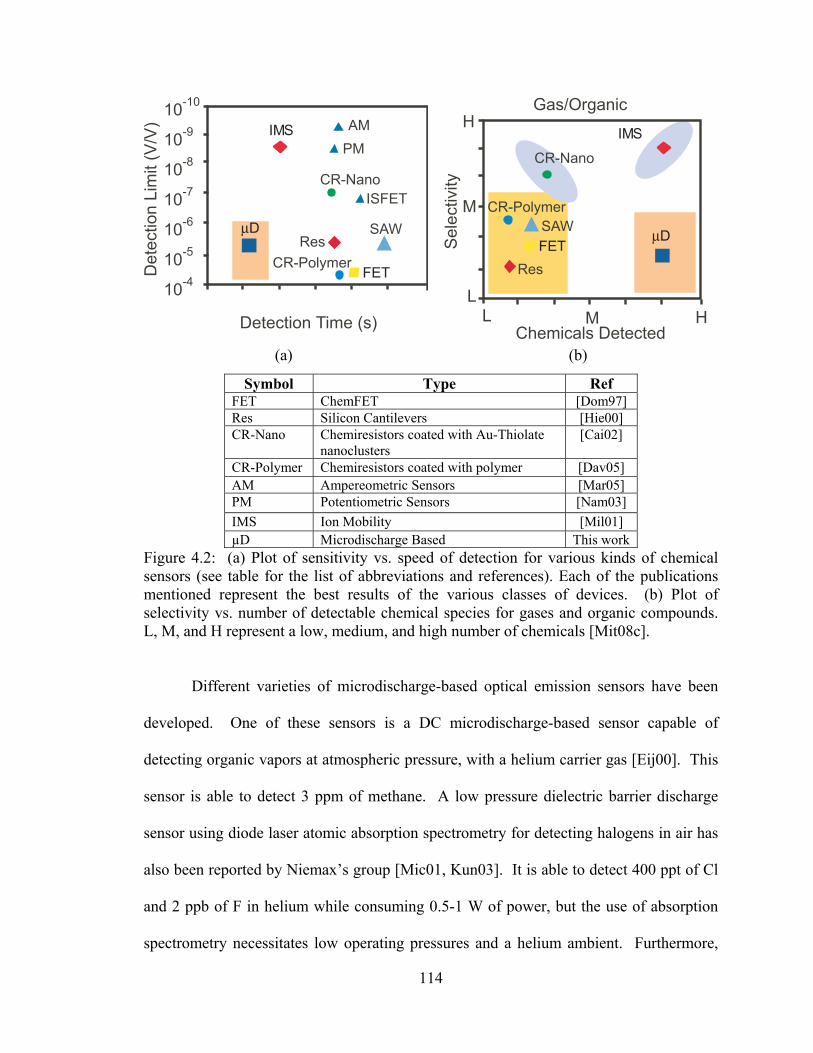
114
Det
ectio
n Li
mit
(V/V
)
Detection Time (s)
10-4
10-5
10-6
10-7
10-8
10-9
10-10
CR-Nano
SAW
CR-PolymerRes
AMPM
ISFET
μD
FET
IMS
Sel
ectiv
ity
Chemicals Detected
CR-Nano
SAWCR-Polymer
Res
HML
H
M
L
Gas/Organic
μDFET
IMS
(a) (b)
Symbol Type Ref FET ChemFET [Dom97] Res Silicon Cantilevers [Hie00] CR-Nano Chemiresistors coated with Au-Thiolate
nanoclusters [Cai02]
CR-Polymer Chemiresistors coated with polymer [Dav05] AM Ampereometric Sensors [Mar05] PM Potentiometric Sensors [Nam03] IMS Ion Mobility [Mil01] µD Microdischarge Based This work
Figure 4.2: (a) Plot of sensitivity vs. speed of detection for various kinds of chemical sensors (see table for the list of abbreviations and references). Each of the publications mentioned represent the best results of the various classes of devices. (b) Plot of selectivity vs. number of detectable chemical species for gases and organic compounds. L, M, and H represent a low, medium, and high number of chemicals [Mit08c].
Different varieties of microdischarge-based optical emission sensors have been
developed. One of these sensors is a DC microdischarge-based sensor capable of
detecting organic vapors at atmospheric pressure, with a helium carrier gas [Eij00]. This
sensor is able to detect 3 ppm of methane. A low pressure dielectric barrier discharge
sensor using diode laser atomic absorption spectrometry for detecting halogens in air has
also been reported by Niemax’s group [Mic01, Kun03]. It is able to detect 400 ppt of Cl
and 2 ppb of F in helium while consuming 0.5-1 W of power, but the use of absorption
spectrometry necessitates low operating pressures and a helium ambient. Furthermore,

115
capacitively coupled sensors have been developed which can operate at atmospheric
pressure but require a helium carrier gas and 1.5 W of power [Gro92, Yos01]. A
microwave-induced microdischarge sensor has also been developed, which can operate at
atmospheric pressure and can detect chemical concentrations of 50 pg mL-1 [Bro02].
This sensor also operates in argon and helium ambient environments and consumes 20 W
of power. Yet another microdischarge-based sensor is a miniature ICP sensor which can
detect 45 ppb sulfur dioxide [Min03]. This device operates at low pressures (0.1-10
Torr), requires an argon environment, and uses 3 W of power. Although all of these
devices are effective, some require operating pressures less than atmosphere or rely on
RF and microwave generation. In general, they require 0.5-10 W of power, are designed
for steady state operation, and have not been tested in high temperature environments.
A DC, microdischarge-based optical emission chemical sensor utilizing pulsed
microdischarges and capable of operating at atmospheric pressure has been further
developed in this work and was reported previously [Mit08a, Mit08b, Mit08c]. This
sensor avoids the constraints of the previously described sensors as it does not require a
reduced pressure for operation, and does not rely on RF and microwave generation.
Additionally, this DC microdischarge-based sensor requires less power and has
demonstrated high temperature operation. It is capable of detecting 50 ppm of carbon in
acetone vapor and has simple, durable components, well suited for high temperature
operation. The sensor consists of thin-film electrodes, between which microdischarges
are created.
Several additional components are necessary to use this chemical sensor in harsh
environments. Purification of a gas sample can become necessary as small amounts of

116
nitrogen dominate emission spectra with intense emission lines [Ark05]. For this purpose
a microdischarge-based gas-purifier (that removes modest quantities of oxygen and
nitrogen) is utilized. A high-temperature microdischarge-based pressure sensor (that
minimizes packaging challenges presented by alternatives) is also included. (See Chapter
3.) These devices operate together in harsh environments to isolate a gas sample,
selectively remove unwanted gas components, and detect the possible presence of a
desired or contaminant gas. This harsh environment sensor differs from previously
designed sensors as it is able to identify numerous gases concurrently time without being
reconfigured.
4.2 DETRIMENTAL EFFECT OF CONTAMINANT NITROGEN IN SPECTRAL
CHEMICAL SENSING
4.2.1 Background
Spectral chemical sensing is limited by the ratio of emission line intensities to
background emissions (relative sensitivity) as opposed to the absolute emission line
intensities (absolute sensitivity). Unlike absolute sensitivity, the relative sensitivity
cannot be increased by traditional methods like amplification or filtering. If the relative
sensitivity is too low, weak emission lines produced by individual gases being examined
will not be detected due to background spectra. This problem of low relative sensitivity
in the presence of strong background spectra is illustrated by examining the ability of
contaminant nitrogen to preclude the detection of other gas species in DC
microdischarges. In particular, its ability to preclude the detection of SF6 is examined.

117
DC microdischarges in SF6 environments have previously been utilized to locally
etch silicon, making the detection of SF6, the identification of the species into which SF6
decomposes, and the characteristics of the microplasmas of particular interest [Wil01a].
Optical emission spectroscopy is used to determine the extent to which SF6 can be
detected with background contamination, and the influence of pressure and applied power
on SF6 spectra. A detailed list of the previously recorded and theoretical emission lines
produced by SF6 dissociation in macroscale plasmas can be found in Appendix 4, as can
the experimental set-up used to obtain microplasma spectra in SF6 environments. A
theoretical discussion of nitrogen’s ability to mask SF6 emission lines, due to their low
relative sensitivity is also presented in this appendix. Several characteristics of SF6
microplasmas are presented in Appendix 5.
4.2.2 Resulting Spectra in SF6
Experiments were performed to determine if SF6 emission lines could be detected
in microplasmas with nitrogen contamination. The emission lines used to detect SF6 have
previously been theoretically and experimentally identified in macroscale SF6 discharges.
In summary, these emission lines include F I lines at 624.0 nm and 703.7 nm, S II lines at
532.1 nm and 545.4 nm, and an emission band comprised of continuously increasing
emission line intensities between 420 nm and 500 nm, which terminates at 500 nm.
The spectra were produced by initiating microplasmas in a vacuum chamber
within a controlled SF6 environment. The microplasmas were created between pairs of
planar copper electrodes with inter-electrode spacing of 500 μm, deposited on 500-μm-
thick glass substrates. The examined discharges were characterized as microplasmas
according to the description of Wilson et al. as they were self-contained glow discharges

118
confined over the cathodes [Wil03a]. These discharges were similar to the discharges
previously used for in-situ silicon etching. However, the power densities of these
microplasmas were higher than the power density used for etching due to the smaller
electrode size. Wilson obtained power densities of 1-10 W/cm2, while these
microplasmas had power densities of 20-4,000 W/cm2.
A two-stage rotary vane roughing pump (Oerlikon Leybold Vacuum Trivac D
16B), accompanying pressure controller (MKS® 600 Series), and external macroscale
pressure transducer (MKS® Baratron® Capacitance Manometer model #627B23TDC1B)
were used to set the pressure between 100 mTorr and 10 Torr. The flow rate of CP grade
SF6 gas (Airgas Inc.) into the chamber was controlled using MKS® Mass-Flo® Series
Mass Flow Controllers (Model #’s 1479A13CR1BM and 1479A21CR1BM). SF6 and air
were introduced and pumped from the chamber at rates of 5.6-260 sccm, to obtain a
constant gas composition and pressure. Power was supplied via a high-voltage power
supply and a 100 kΩ ballast resistor was connected in series with the anode to limit
current. The optical spectra produced were measured using an Ocean Optics USB2000TM
spectrometer.
The spectra produced by microplasmas in SF6 showed no indication of SF6, or its
dissociated by-products, and only displayed emission lines caused by contaminating
nitrogen. The microplasma spectra in SF6 were obtained in almost pure SF6
environments, at total pressures between 100 mTorr and 10 Torr with currents between
500 µA and 4 mA. The spectra consisted of numerous closely spaced lines, as opposed
to single lines as in atomic spectra, because the different energy levels in molecules have
structures corresponding to many different vibrational and rotational levels. Figure 4.3(a)

119
shows a typical spectrum produced in SF6, regardless of the pressure or gas flow rate.
The spectrum contains no indication of fluorine, ionized sulfur, or an SF6 emission band,
and is dominated by N2 and N2+ lines. The previously recorded molecular nitrogen
emission lines at wavelengths of 316.0 nm, 337.1 nm, 357.7 nm, and 380.5 nm were all
observed. Figure 4.3(b) shows the spectrum produced in SF6 after the spectrum produced
in air, before SF6 introduction, has been subtracted out. This does not show any
indication of SF6 dissociation either. However, time evolution of the microplasmas from
spectrum to spectrum could have affected this spectral subtraction.
0
100
200
300
400
200 300 400 500 600 700 800Wavelength (nm)
Inte
nsity
(a.u
.)
316 nm (N2)
337 nm (N2)358 nm (N2)
381 nm (N2)
703 nm (F)
624 nm (F)
545 nm (S+)532 nm (S+)
No Indication of SF6
(a)
200 300 400 500 600 700 800
Wavelength (nm)
Inte
nsity
(a.u
.)
0
500
1000
1500
2000
2500 337 nm (N2)
316 nm (N2)
358 nm (N2)
381 nm (N2)
(b)
No Indication of SF6
0
200
400
600
800
1000
1200
200 300 400 500 600 700 800Wavelength (nm)
Inte
nsity
(a.u
.)
337 nm (N2)
316 nm (N2)
358 nm (N2)
391 nm (N2+)
381 nm (N2)
(c)
-1200
-1000
-800
-600
-400
-200
0
200
200 300 400 500 600 700 800Wavelength (nm)
Inte
nsity
Diff
eren
ce (a
.u.)
391 nm (N2+)
428 nm (N2+)
(d)
Figure 4.3: Microplasma emission spectra in air and SF6 at 3 Torr. All figures use the same arbitrary unit scale for the intensity. (a) SF6 environment with 800 V and 500 μA. (b) SF6 environment with 1,000 V and 2.7 mA after the spectrum produced in air has been subtracted out. (c) Air environment with 500 V and 500 μA. (d) Average normalized difference between SF6 and air emission spectra recorded between 400 mTorr and 10 Torr.

120
Figure 4.3(c) shows a reference spectrum recorded in an air environment with the same
applied current and pressure used for the SF6 spectrum in Fig. 4.3(a), for comparison.
The spectra are almost identical except for the increase in N2+ emission line intensity as
indicated by the previously mentioned 391.4 nm line. Figure 4.3(d) shows the average
difference between 12 normalized spectra recorded in SF6 and 12 in air at pressures from
400 mTorr to 10 Torr.
The spectra were all normalized to the strongest N2 emission (337.1 nm) before
the differences were calculated and averaged for each emission line. The N2+ emission
line (391.4 nm) intensity in microplasmas was significantly reduced by a SF6
environment relative to an air environment as indicated by the negative peak. A
reduction of N2+ in an SF6 environment is caused by the highly efficient charge transfer
reaction [Arn04]:
N2+ + SF6 SF5
+ + N2 + F (4.1)
Given this reaction, it may be possible to use the N2+ emission line intensity to detect SF6
in microplasmas. The SF6 gas flow rate and pressure had no effect on the resulting
spectra. Identically shaped titanium electrodes produce similar spectra to those obtained
with copper electrodes.
Detailed views of the 400-510 nm regions of the spectra produced by
microplasmas in air and SF6 are shown in Fig. 4.4, where the molecular emission band
has previously been observed. Even under magnified examination of these regions, there
is little discernable difference between the spectra and no indication of a molecular band
between 420 nm and 500 nm.

121
0
25
50
75
100
400 425 450 475 500Wavelength (nm)
Inte
nsity
(a.u
.)
(a)AirRegion of emission band
0
25
50
75
100
400 425 450 475 500Wavelength (nm)
Inte
nsity
(a.u
.)
(b)SF6Region of emission band
Figure 4.4: Emission spectra in (a) air and (b) SF6 between 400 nm and 510 nm where the molecular emission band produced by SF6 has been observed. Three consecutive measurements are averaged in each environment.
In macroscale discharges, the emission lines created by SF6 in discharges are
difficult to detect due to the low relative sensitivity of SF6 compared to contaminating gas
emission lines. Small amounts of nitrogen dominate SF6 emission spectra at high and
low pressures when both positive and negative high voltages are used to induce the
discharges [Tei84, Tei85]. This low relative sensitivity is demonstrated by observing that
in an environment of SF6 + 470 ppm N2, SF6 and N2 emission lines have equal intensities.
In an environment of SF6 + 1% N2, SF6 emission lines are approximately one-fourth as
intense as N2 emission lines and in an environment of SF6 + 50% N2, SF6 emission lines
are not detectable [Cas91]. The minimum excitation energy for N2 is 8.399 eV [Sul01],
which is slightly below the lowest level excitation energy of SF6, the 1 t1g → 6 a1g
transition at 9.6 eV and 9.9 eV for triplet and singlet components respectively [Raj06].
The ionization energies of fluorine, SF6, and N2 range between 15.33 eV and 17.42 eV,
which does not explain the differences in emission line intensity [Lid49, Hub79, Asg00].
The dissociation energy required to separate SF6 into SF5 and F is 9.6 eV, which is less
than the ionization energy of N2 and does not explain the line intensity difference
[Raj06]. However, the difference in emission line intensity is explained by the relatively

122
small excitation cross section of SF6 in comparison to nitrogen [Zen91]. Creating
discharges with lower applied currents also increases the ability of nitrogen to dominate
SF6 emission lines, precluding SF6 detection.
It is apparent that it is extremely difficult to detect SF6 in microplasmas in the
presence of contaminating nitrogen, which leads to low relative sensitivity. Whereas on
the macroscale SF6 can be detected with 1% nitrogen in the environment, this is not the
case in microplasmas. This suggests that another issue has been encountered. One
explanation is that the dielectric property of SF6 is causing the power to be shunted to
nitrogen in the discharge, which increases the amount of nitrogen excitation and decrease
the amount of SF6 excitation. Another explanation previously suggested is that the lower
currents used in these microplasmas, 500 µA - 4 mA are limiting SF6 detection. The
inability to detect SF6 in microplasmas demonstrates that accurate chemical sensing
depends on the removal of contaminating nitrogen.
4.3 USING MICRO-SIPS FOR GAS PURIFICATION
4.3.1 Concept, Operation, and Design of Gas Purifying Micro-SIPs
Given the detrimental effect nitrogen has on the detection of gases using spectral
chemical sensing, as outlined in the previous section, microscale-sputter-ion pumps
(micro-SIPs) which can remove nitrogen and oxygen provide a means of improving gas
detection. If nitrogen and its background emission lines are removed from a sample,
small concentrations of gases with weak emission lines can be detected and the relative
sensitivity of the sensor is increased. The purification ability of micro-SIPs is a primary
motivation for the development of the chemical sensing microsystem.

123
Micro-SIPs, as described in detail in Chapter 2, operate through the creation of
DC microdischarges between two titanium thin-film electrodes. These microdischarges
sputter the titanium cathodes of the micro-SIPs, bonding this titanium to gas molecules,
and removing these molecules from the environment. Their ability to reduce pressure in
sealed cavities has been discussed in Chapter 2 but their ability to purify gas
environments has not. The sputtered titanium has been shown to react selectively with
nitrogen and oxygen on the macroscale without interacting with helium, carbon, sulfur,
and other gases of interest, making these devices ideal for removing air contamination
[Den67].
The micro-SIPs used for gas purification in this application have circular anodes
surrounded by large cathodes as shown schematically in Fig. 4.5 and are similar to the
version 2 design previously described. The cathodes have areas of 1.52 mm2 and
discharge gaps of 50 µm. While the anode and cathode dimensions used for gas
purification are identical to version 2 micro-SIPs, only three anode/cathode pairs are
included and the entire device has an area of 25 mm2. DC voltages of 1,000 V are
applied to induce rapid purification, and a 2.5-MΩ ballast resistor is used. The micro-
SIPs are fabricated as previously described using titanium as the electrode material as it
has the ability to bond selectively with nitrogen and oxygen.

124
+-Power Supply (VP)
Micro-SIPs
I Multimeter
2.5 MΩ ballast resistor
Microdischarge
Figure 4.5: Gas-purifying micro-SIPs. A DC voltage is applied to selectively remove nitrogen and oxygen.
4.3.2 Results and Discussion
The gas purification provided by micro-SIPs was evaluated by examining the
spectra produced by microdischarges over time in gas samples with known initial gas
concentrations. A micro-SIP was operated in an environment containing 99.25% helium
(99.995% pure) and 0.75% air to test the purification abilities at a pressure of 200 Torr.
The micro-SIP was enclosed in a re-sealable glass package, 2.5 cm in diameter (4 cm3).
The gas concentration was set by MKS® Mass-Flo® Series Mass Flow Controllers
(Model #’s 1479A13CR1BM and 1479A21CR1BM), accompanying pressure controller
(MKS® 600 Series), and external macroscale pressure transducer (MKS® Baratron®
Capacitance Manometer model #627B23TDC1B). The air initially in the package was
removed by a two-stage rotary vane roughing pump (Oerlikon Leybold Vacuum Trivac D
16B). A needle valve was used to seal the re-sealable package while the micro-SIP
operated.
Helium is the most commonly used carrier gas in gas chromatography, and was
thus used as a carrier gas. The strongest nitrogen and oxygen emission line intensities
were normalized to that of helium to account for variations in discharge intensity. A
56.5x reduction in nitrogen and a 16.2x reduction in oxygen were observed over five

125
hours as shown in Fig. 4.6. The final concentrations of the contaminant gases, based on
the measured reduction in emission line intensities compared to the initial intensities,
were 90 and 70 ppm, respectively. Figure 4.7 shows spectra produced before and after
purification. The nitrogen and oxygen emission lines were almost completely removed,
while a helium emission line remained, indicating that helium was not removed to a
detectable extent. Nitrogen and oxygen produced strong background emission lines
despite their relatively low concentrations in the first recorded spectrum (Fig. 4.7(a)),
confirming the previous findings and demonstrating the advantage of removing these
emission lines when detecting other gases.
0
0.1
0.2
0.3
0.4
0.5
0.6
0 1 2 3 4 5
Gas
in S
ampl
e (%
)
Time (hours)
Rapid absorption
Stable concentrationNitrogen
Oxygen
Contaminants in He Sample (%)
Figure 4.6: Percentage of contaminants (nitrogen and oxygen) in a helium sample during gas purification, showing the thorough removal of the unwanted gases.

126
376 nm (O+)
667 nm (He)337 nm (N2)
0
250
500
750
1000
200 300 400 500 600 700 800
Inte
nsity
(a.u
.)
Wavelength (nm)0
250
500
1000
750
200 300 400 500 600 700 800
376 nm (O+)
667 nm (He)
337 nm (N2)
Inte
nsity
(a.u
.)
Wavelength (nm)(a) (b)
777 nm (O2)
777 nm (O2)
Figure 4.7: Spectra of the pump discharge in 99.25% helium with air contamination at 200 Torr (a) before purification and (b) after purification. Small amounts of nitrogen cause intense emission lines compared to helium at time = 0, demonstrating the necessity of nitrogen removal.
4.4 HARSH ENVIRONMENT CHEMICAL SENSOR
4.4.1 System Concept
An exploratory harsh environment chemical sensing microsystem has been
developed to integrate and expand upon the operation of the described micro-SIP
(Chapter 2 and Chapter 4, Section 4.3) and microdischarge-based pressure sensor
(Chapter 3). Additionally, a microdischarge-based optical emission sensor is included to
perform the sensing. The ability of the three microdischarge-based components to
function at high temperatures makes them well suited to operate concurrently in a harsh
environment system. These three devices are hermetically sealed inside a ceramic
package with a quartz lid while micromachined valve(s) control the gas flow into and out
of the package as shown in Fig. 4.8. The tubes connecting the microscale components to
one another and to the external components have a 1 mm inner diameter, large enough to
accommodate a high throughput if necessary.

127
Microdischarge - Based Optical Emission Sensor Gas Purifying
Micro-SIP Microdischarge - Based Pressure Sensor
Bidirectional Micromachined Valves
Unknown Gas Inlet
Ceramic PackageQuartz Lid
PumpHe
Optical Fiber
Spectrometer
EXTERNAL COMPONENTS
HIGH TEMPERATURE COMPONENTS
Filter
Figure 4.8: Schematic of the entire harsh environment chemical sensing system.
4.4.2 System Optical Emission Sensor
While the micro-SIP and pressure sensor have been previously described in
Chapters 2 and 3 respectively, the optical emission chemical sensor and valves specific to
this system have not been discussed. The optical emission chemical sensor (chemical
detector) operates by creating pulsed microdischarges between thin-film anode/cathode
pairs to fractionate and exciting gas species, shown schematically in Fig. 4.9(a). The
spectra emitted from the microdischarges are characteristic of the energy transitions of
the individual fractionated gases. This optical emission sensor is based on previously
developed sensors which utilized a two electrode configuration and a three electrode
flashFET configuration, for reduced power consumption, to detect chemicals at
atmospheric pressure [Mit08a]. This sensor is able to detect carbon in acetone vapor at
concentrations as low as 50 ppm. In addition, these microdischarge-based sensors have
been used in a portable handheld gas detection system [Mit08b]. An optical fiber directly

128
opposite the microdischarges, outside the quartz lid, couples the emitted light to a
spectrometer (Ocean Optics USB2000TM). The recorded spectra are examined to
determine the unknown gas composition based on the characteristic emission lines.
Pulsed microdischarges have significant afterglow periods, lasting 7 ms, and integrating
both the afterglow and initial discharge emissions for up to 10 ms in the spectrometer
improves the ability to detect less dominant peaks [Mit08a]. This sensor is not designed
for dusty or dirty environments, as contaminants short the sensor electrodes and block
transmission through the quartz lid.
(a) (b)
Figure 4.9: Microdischarge optical emission sensor (chemical detector) used to detect carbon and other vapors through recorded spectra. (a) Schematic. (b) Photograph.
The optical emission chemical sensors are of the three electrode flash-FET
configuration, but are used in the traditional two electrode discharge mode of operation as
shown in Fig. 4.9(b). As microdischarges have been shown to be confined over the
cathode, relatively large cathodes, 1.82 mm2, are used to produce a large glow region for
improved optical emission detection. A 100-µm discharge gap separates the electrodes
Optical FiberPC DAQ Card
2.7 MΩ
Spectrometer Trigger
Power Supply (VP)
20 MΩ ballast resistor

129
and a voltage of 1,000 V is used to create the microdischarges. Computer-controlled
pulses trigger the microdischarges and spectrometer. A 20-MΩ ballast resistor is used.
4.4.3 System Bidirectional Micromachined Valves
The bidirectional micromachined valves control the flow of gas into and out of
the package and have separate inlets and outlets. They operate by depressing a bulk
silicon micromachined plate against a Corning #7740 Pyrex glass substrate with inlet and
outlet holes (Fig. 4.10). A commercially-available, multilayered piezoelectric PZT stack
drives the silicon valve plate (Physik Instrumente, Germany, PL055), and has a footprint
of 5 x 5 mm2 with a height of 6 mm. The materials in the valves are selected so that the
temperature expansion mismatches do not inhibit device operation over a wide range of
temperatures. Macor™, a glass mica ceramic, is used as the primary packaging material.
It can be easily machined with precision, and has a thermal expansion coefficient of 7.4
ppm/K. In addition, it has zero porosity, does not outgas in vacuum environments, and
can be used with epoxy to provide a hermetic seal. The ceramic enclosure measures 1 x 1
x 1 cm3, and has a 6 mm deep cavity, with 1 mm thick walls on all four sides. A
thorough description and test results are in [Par08].

130
Figure 4.10: Microvalve concept: The valve consists of ceramic-PZT-Si-glass structure. A PZT stack actuator moves the silicon plate to open or close the valve. Micro-groove patterns are fabricated on the silicon plate to increase the flow area [Par08].
4.4.4 System Operation and Fabrication
The system utilizes bidirectional valves, a micro-SIP, a microdischarge-based
pressure sensor, and an optical emission sensor to isolate, purify, and sense gas samples.
One possible configuration for field use is shown in Fig. 4.8. Remote components,
external to the harsh environments, include a two-stage rotary vane roughing pump
(Oerlikon Leybold Vacuum Trivac D 16B), accompanying pressure controller (MKS®
600 Series), backfilling gas tank, and a spectrometer. In the proposed configuration, a
sample is introduced into the empty package through one micromachined valve while a
second connects the package to the external components for backfilling and pressure
regulation. After a sample is introduced, the package is backfilled with an inert gas while
the internal pressure sensor monitors the pressure in the package and the external pump
controls it. When the desired pressure is reached, the package is isolated by closing the

131
valves. The gas-purifying micro-SIP is then operated while the chemical sensor is
pulsed, recording spectra over time. The micro-SIP continues to operate until the relative
sensitivity of unknown gas lines to background nitrogen lines is high enough for
detection of the unknown gas, if present.
All three microdischarge-based devices were fabricated on a single wafer with
two masks to simplify processing using the same process flow as the micro-SIPs in
Chapter 2 and the pressure sensors in Chapter 3. A Ti film (1 µm thick) and an Au film
(500 nm thick) were thermally evaporated onto #7740 PyrexTM glass wafers (500 µm
thick) without removing the wafers from vacuum. The contact pads were patterned on
the gold layer using photolithography and etched using Transene GE-8148 gold etchant,
which does not etch titanium. The electrodes were then patterned in the titanium layer
using photolithography. The final devices had footprints of 25 mm2 each, with a
combined active area of 10.5 mm2. Solder and epoxy were used to connect the devices
and seal them in 0.33 cm3 ceramic packages as shown in Fig. 4.11.
Figure 4.11: System before sealing in ceramic package next to a U.S. penny.

132
4.4.5 Results and Discussion
For the overall system, preliminary testing was performed at 200°C based on
anticipated requirements [Sha06], although it can potentially operate at much higher
temperatures. The setup for this testing utilized only one micromachined valve, through
which both the sample and backfilling gas were introduced. Acetone vapor, 10,000 ppm,
was introduced as a carbon source and helium was used to backfill the system to a final
pressure of 200 Torr. The system was raised to 200°C and the optical emission sensor
was operated every 20 seconds to determine gas concentrations based on emission line
intensities. The sensor was operated for 50 ms and the emissions were integrated for 300
ms to capture the afterglow.
Time (minutes)
0
2
4
6
8
10
0 1 2 3 4 5
Impr
ovem
ent F
acto
r
[I(516nm) / I(337nm)]t[I(516nm) / I(337nm)]t=0
Figure 4.12: Ratio of carbon to nitrogen emission line intensity during gas purification at 200°C, based on their strongest emission lines.
The micro-SIP was operated and the strongest carbon emission line (516.4 nm)
increased in intensity by 8x relative to strongest nitrogen emission line (337.1 nm) as
shown in Fig. 4.12. This purification increased the ability to detect carbon with respect to

133
the contaminant gases by increasing the relative sensitivity. Figure 4.13 illustrates the
recorded spectra before and after purification, indicating the increased emission line
intensities of carbon and CN relative to the contaminant nitrogen.
(a) (b)
0
250
500
750
1000
Inte
nsity
(a.u
.)
200 300 400 500 600 700 800Wavelength (nm)
667 nm (He)
516 nm (C2)337 nm (N2)
388 nm (CN)667 nm (He)
516 nm (C2)
337 nm (N2)
388 nm (CN)
0
250
500
750
1000
Inte
nsity
(a.u
.)
200 300 400 500 600 700 800Wavelength (nm)
Figure 4.13: Spectra of acetone sample backfilled with helium during gas purification at 200°C. (a) Spectrum recorded before purification, showing strong nitrogen emissions and low C2 emissions. (b) Spectrum recorded after purification, showing diminished nitrogen and increased CN and C2 emissions.

134
CHAPTER 5
CONCLUSION
Microdischarge-based devices have been developed which control the pressure in
sealed cavities, through sensing and actuation, at room temperature and at high
temperatures. These devices have been combined with an optical emission sensor to
create a harsh environment chemical detection microsystem.
5.1 DISSERTATION SUMMARY
Chapter 2 outlined on-chip sputter-ion pumps and their use in the controlled
reduction of pressure in large cavity packages. The devices utilized pulsed and DC
microdischarges between thin-film titanium electrodes patterned on glass substrates. The
micro-SIPs functioned in hermetically sealed cavities, without heating surrounding
devices, and provided control over the amount of air and humidity removed from the
inside of the cavity.
Micro-SIP pumping performance was characterized though experimental and
modeling results. The influence of (1) the micro-SIP design, (2) the environment in
which micro-SIPs were operated, (3) the mode of micro-SIP operation, and (4)
microdischarge characteristics on micro-SIP pumping operation were investigated. These
were explored through examining micro-SIP operation with varied discharge gap spacing

135
at varied pressures. The gas removal rates were found to depend on both the initial
pressure and discharge gap spacing, and micro-SIPs with smaller discharge gaps
operating at higher initial pressures removed air at the greatest rate. A theoretical model
outlining the dependency of gas removal rates on microdischarge parameters was
developed and was able match the experimentally obtained results. In an air
environment, these devices reduced the pressure by 168 Torr in a 6.33 cm3 cavity and
126 Torr in a 2.2 cm3 cavity when starting at atmospheric pressure. Oxygen, nitrogen,
and air pressures were reduced at rates of 11.5 Torr/h, 3.4 Torr/h, and 7.2 Torr/h,
respectively, starting at 200 Torr. The pumps have been shown not to remove helium
from the environment. Water vapor concentrating was reduced in a sealed package at a
rate of 6% relative humidity per hour, starting with 61% relative humidity. Using pulsed
discharges, 25 ms in duration, as opposed to DC discharges with same amount of energy,
and enough time, micro-SIPs removed five times as much air. This indicated that shorter
pulses were more energy efficient despite their slower removal rates. These data
concerning the operation and characteristics of micro-SIPs suggest that they are
promising for low-temperature pressure control of vacuum-sealed packages in microscale
systems applications.
Chapter 3 outlined microdischarge-based pressure sensors, which operate by
measuring the change, with pressure, in the spatial current distribution of pulsed DC
microdischarges. These sensors are well-suited for high temperature operation because
of the inherently high temperatures of the ions and electrons in the microdischarges.
They provide an electrical readout, avoiding an intermediate transduction step, which can
be convenient in some cases. The absence of a diaphragm, which is commonly used in

136
piezoresistive and capacitive pressure sensors, also provides natural tolerance for
overpressure and consequently, mechanical robustness.
Two sensor versions were presented and demonstrated. The first type used three-
dimensional arrays of horizontal bulk metal electrodes embedded in quartz substrates
with electrode diameters of 1-2 mm and 50-100 µm inter-electrode spacing. These
devices demonstrated they could operate over a range of at least 10-2,000 Torr, at
temperatures as high as 1,000˚C, and it is expected these sensors could potentially
operate at temperatures below room temperature and over larger dynamic pressure
ranges. The maximum measured sensitivity was 5,420 ppm/Torr at the low end of the
dynamic range and 500 ppm/Torr at the high end, while the temperature coefficient of
sensitivity ranged from -925 ppm/K to -550 ppm/K. Sensors of the second type used
planar electrodes, and had active areas as small as 0.13 mm2, small enough to permit
hybrid or monolithic integration with other components that constitute functional
microsystems. These devices, when tested in a chemical sensing system flowing helium
as a carrier gas, had a maximum sensitivity of 9,800 ppm/Torr, a dynamic range of 25-
200 Torr, and a temperature coefficient of sensitivity of approximately -1,412 ppm/K.
The sensitivity achieved compared favorably with conventional piezoresistive and
capacitive pressure sensors of similar size.
Chapter 4 outlined a system for gas purification and gas phase chemical detection
in harsh environments that integrated the micro-SIP and microdischarge-based pressure
sensor. In particular, it described the need for removal of contaminant gases such as
nitrogen when performing spectral chemical sensing. It then presented the ability of
micro-SIPs to purify gas environments from contaminating nitrogen and oxygen,

137
achieving a 56.5x reduction in nitrogen concentration relative to helium. Finally, it
described the chemical detection system which utilized three microdischarge-based
devices: pressure sensor, gas purifier, and optical emission sensor. This system used the
pressure sensor to measure the incoming sample and backfilling gas. The micro-SIP
purified the microsystem environment of contaminating nitrogen and oxygen, increasing
the strongest carbon emission by 8x relative to nitrogen. The system was used for carbon
detection at temperatures of at least 200°C.
New microtransducers have been developed, providing advantageous options for
microsystems and expanding the field of microdischarges to a larger range of sensing and
actuating roles. The devices have expanded the field by providing alternatives which are
small, simple to fabricate, and inexpensive. In addition, they provide electronic
transduction and operate in both low and high temperature environments. These qualities
are desirable in most microscale devices as demonstrated by the numerous potential uses.
Additionally, the utility of microdischarges as a transduction method has been expanded.
The developed devices have demonstrated that through simply measuring microdischarge
characteristics, useful information such as pressure can be determined. The use of
microdischarges will continue to expand, potentially simplifying currently complex
microscale devices with simple electrode structures and ionized gas.
5.2 SUGGESTIONS FOR FUTURE WORK
5.2.1 Utilizing Micro-SIPs to Reach High Vacuum (10-6 Torr)
In the work presented in this thesis, micro-SIPs were operated at pressures
between 30 Torr and 760 Torr. A logical progression is the development of micro-SIPs

138
capable of reducing the pressure to high vacuum levels (10-6 Torr) in microscale
packages.
A micro-SIP capable of generating a high vacuum environment would have
several advantages over other pumping technologies which have been proposed or
previously utilized, outlined in Chapter 2. Microscale orbitron pumps have been
proposed, but not developed, which would use external electron guns to introduce high
energy electrons instead of utilizing magnetic fields. This would put orbitron pumps at a
disadvantage compared to a micro-SIP, due to the power consuming electron emitters.
Non-evaporable getters could be included in hermetically sealed environments to remove
gases through oxide formation, hydride formation, and surface chemisorptions.
However, NEGs typically require activation temperatures of 300ºC or higher, which can
damage packaged devices while a micro-SIP would not substantially heat the surrounding
environment as shown in Chapter 2. Additionally, a micro-SIP could set the vacuum
level and pumping speed through user controlled electrical means. Microscale peristaltic
pumps would be of limited use at low pressures, due to the long mean free path length,
and a microscale turbomolecular pump would require a very high rotation rate, due to the
small blade radius, to match the performance and rotation speed at the blade tip of the
macroscale counterpart. A high vacuum micro-SIP would be advantageous as it would
have no moving parts, increasing durability and reducing fabrication complexity.
The proposed micro-SIP for high vacuum generation would utilize thick titanium
foil electrodes and a permanent magnet to create Penning discharges as shown in Fig. 5.1.
The magnetic field would increase ionization, as in macroscale-SIPs, by causing the
electrons emitted from the cathode to move in long helical trajectories which would

139
improve the chances of collision with gas molecules [Sch99, Wel03]. The field would be
necessary as at these low pressures (p) and small discharge gaps (d), a very high
breakdown voltage is required to induce ionization (without a magnetic field) as the mean
free path length at 10-6 Torr is 51 m. Macroscale-SIPs utilize magnetic fields of 600-
1,500 Gauss and the pumping rate is directly related to field strength [Rut99, Sch99].
Figure 5.1: Schematic of a micro-SIP and accompanying magnet in a sealed package with outlet ports.
Miniaturized magnets have been used to enhance the parameters of DC
microdischarges and have been shown to increase confinement, decrease sheath width,
lower breakdown voltages, and increase current [Wil04, Ito08]. The current in
magnetically enhanced microdischarges has been shown to increase with magnetic field
strength, at a constant applied voltage, in a manner similar to macroscale discharges
[Wen90]. Miniature magnets have also been used to increase the etch rate of silicon
using a SF6 microdischarge by 3x in localized areas and they have been integrated with a
micro-machined Geiger counter to enhance the RF transmission from microdischarges
initiated by incident beta particles [Eun08]. They have also been shown to increase
electron magnetization at lower pressures [Ito08]. Previously, microscale magnets

140
creating magnetic fields of 3,000 Gauss were patterned and used [Fis01, Wil04]. For a
micro-SIP, a niobium magnet should be considered in a magnetic flux circuit
configuration (Fig. 5.1) to create the requisite magnetic field. The possible use of an
electromagnet to assist the permanent magnet should also be considered.
The high vacuum micro-SIP could also be operated with little power using power-
saving techniques for discharge initiation and energy control. A high impedance third
electrode would be powered through a series inductor, facilitating discharge initiation
with a relatively low voltage pulse between the anode and cathode; this would also allow
the discharge current to be controlled through the anode, independently of the discharge
initiation conditions [Mit08a, Mit08b]. Using this technique, the energy per discharge
pulse has been reduced from 0.467 mJ to 2.5 µJ at 140 Torr, indicating its potential for
micro-SIP energy reduction. A pulsed discharge-powering scheme should be used as it
has been shown to increase power efficiency in Chapter 2. For example, bursts of pulses
10 ms in duration could be applied at a rate of 10 Hz, using 1 mJ per burst, consuming an
average of 10 mW.
The electrode lifetime could be increased by using thick-film titanium electrodes
patterned by micro-electro-discharge machining (µ-EDM) [Tak02, Tak04, Tak06, Ric08]
or RIE [Aim04, Par07]. Electrodes 100-µm thick would provide extended lifetime over
thin-film evaporated or sputtered electrodes, and could be used to create a cathode
containing 5.66 x 10¹⁸ atoms. If this cathode is used, it would contain over six orders of
magnitude more than the 3.26 x 10¹² molecules of nitrogen and oxygen in a 1 mm3 pump
cavity at 100 mTorr, and three orders of magnitude more than the 1.63 x 10¹⁵ molecules
present at 50 Torr. This titanium:gas molecule ratio would theoretically allow the pump

141
to be used for thousands of evacuations. Additionally, the use of pulse discharges would
drastically increase device lifetime.
Several scientific and technical challenges would be presented in the development
of this unique pumping mechanism. The electron response to the applied magnetic field
must be understood to ensure the electrons are forced into spiral orbits, maximizing
ionization. This could be accomplished through modeling. Additionally, a localized
magnetic field of over 3,000 Gauss would be required from a microscale magnet. This
could be addressed by increasing the localized field using appropriately shaped poles in
the magnetic flux circuit. To prevent device contamination from sputtered titanium
atoms, the micro-SIP could be situated in a separate cavity.
5.2.2 Harsh Environment Chemical Sensor Packaging
The developed harsh environment chemical sensor (Chapter 4, Section 4.4) was
packaged in a DIP package for testing purposes, but a package which allows gas
sampling in muddy, aqueous, or dusty environments would be advantageous for real-
world use. A package with a permeable membrane, possibly constructed of GOR-TEX®
fabric, could be developed to allow gas sampling. In addition, an optical fiber could be
integrated with the package to secure the lens attached to the fiber optic cable. This
would improve the consistency of the recorded spectra. A schematic of a potential
packaging strategy is shown in Fig. 5.2.

142
Semi-permeable Membrane
To External Components
Microdischarge Devices
Harsh Environment
Integrated Fiber Optic
Figure 5.2: Schematic of harsh environment chemical sensor package with semi-permeable membrane and integrated fiber optic cable.
5.2.3 Selective Growth of Doped Nanowires Using Microdischarges
The current method of synthesizing doped SnO2 nanowires for thin-film
transistors (TFTs) does not allow selective growth in regions or patterns on a substrate
without pre-growth patterning of the catalyst layer. Localized microdischarges may
present a method of influencing growth through the local application of additional energy
in the form of fast-moving ions and heat, as microdischarges have been shown to increase
the gas temperature at the cathode by as much as 280˚C at 250 Torr [Boe05, Kus05].
This would allow for post-wafer-processing growth control and pattern generation. This
method could also potentially be used to “write” nanowires by scanning a
microdischarge. This has been initially explored and described in Appendix 6, however
further investigation is required to determine the precise temperature at which nanowires
are formed on the substrate. Holding the substrate slightly below this temperature would
allow a slight temperature increase, caused by a microdischarge, to locally heat a region
to a suitable temperature for growth.

143
APPENDICES

144
APPENDIX 1
CALCULATING MICRODISCHARGE PARAMETERS
The DC discharge parameters governing charged species and ionization in
microdischarges can be calculated in both the discharge and the cathode sheath regions,
as steady-state microdischarges operate similar to normal or abnormal glow discharges.
In DC discharges, the electrons are drawn towards the anode, whereas the positive ions
are drawn to the cathode forming a positively charged sheath around it. Upon cathode
impact, the energetic ions eject high energy secondary electrons from the cathode, which
sustains the microdischarge by ionizing additional neutral molecules and continuing the
breakdown process. Current in the discharge is carried primarily by the faster moving
electrons while current in the cathode sheath is composed of a combination of positive
ions impacting the cathode from the microdischarge and secondary electrons ejected from
the cathode upon ion impact. In microdischarges, the width of the sheath and the size of
the microdischarge can be similar [Kus05]. A glow microdischarge created in a
microdischarge-based pressure sensor is examined as are the formulas used for parameter
calculations. The initial transient current pulses encountered during discharge initiation
are not discussed in this Appendix. Additionally, the calculated parameters consider
macroscale DC discharges, which typically underestimate the electric field strength in the

145
sheath region of microdischarges and do not consider the non-Maxwellian electron
energy distribution function encountered in microdischarges.
A1.1 MICRODISCHARGE PARAMETERS IN A PRESSURE SENSOR
The electric field strength, ionization frequency, and other parameters are
calculated for DC, glow microdischarges operating in steady-state, which are created and
utilized by devices in this thesis. The microdischarge created between a parallel disk-
shaped planar anode and a torus-shaped planar proximal cathode in a microdischarge-
based pressure sensor is examined in detail. The electrodes in the sensor are composed of
stainless steel and are spaced 50 µm apart, 125 µm thick, and 1 mm in diameter. An
applied voltage of 1,000 V is considered with a maximum DC current of 300 µA. The
electron temperature is assumed to be 3 eV (34,815 K) away from the cathode with an
ion temperature of 0.03 eV (621 K) in a 23ºC (296 K) ambient environment, based on
previous microdischarge models [Kus05]. The parameters are calculated over the actual
sensor operating range, from 10-2,000 Torr and 23-1,000ºC in a nitrogen environment.
The parameters describing the ions, electrons, ionization, and the electric field strength in
the primary discharge are listed in Table A1.1. The microdischarge radius is measured
along the axis parallel to the electrodes.
The ambient pressure and temperature affect all of the parameters as indicated by
the calculated ranges. The effect on discharge size and electric field strength is
examined. As the pressure increases, and as the temperature decreases, the discharges
become exponentially more confined as shown in Fig. A1.1. However, as the discharge

146
radius is decreased, an increase in ionization is required and the electric field strength
increases in response. The current is primarily limited by external ballast resistors.
Table A1.1: DC glow microdischarge operating parameters in a microdischarge-based pressure sensor, calculated over the range of 10-2,000 Torr and 23-1,000ºC.
Parameter Symbol Units Value at 23ºC and 10 Torr
Range over Pressure Sensor
Operation
Plasma Density no cm-3 8.5 x 10¹³ 8.5 x 10¹³ – 1.1 x 10¹⁵
Debye Length λDe µm 1.4 0.39 – 1.4 Electron
Temperature Te eV 3 3.0 – 3.1
Electron Momentum
Transfer Frequency
νme Hz 5.0 x 10¹⁰ 1.2 x 10¹⁰ – 1.0 x 10¹³
Electron Mobility µe m2/ V · s 3.5 0.018 – 15 Electron Velocity ve m/s 1.2 x 10⁶ 1.2 x 10⁶
Ion Temperature Ti eV 0.056 0.055 – 0.14 Ion-Neutral Interaction Frequency
νmi Hz 1.2 x 10⁸ 4.4 x 10⁷ – 2.4 x 10¹⁰
Ion Mobility µi m2/ V · s 2.9 x 10⁻² 1.5 x 10⁻⁴ – 7.9 x 10⁻²
Ion Velocity vi m/s 700 700 –1,100 Ion Diffusion Coefficient Di m2 / s 1.6 x 10⁻² 8.1 x 10⁻⁶ – 1.1 x
10-2
Ambipolar Diffusion
Coefficient Da m2 / s 9.0 x 10⁻² 4.5 x 10⁻⁴ – 0.26
Ionization Rate νiz Hz 4 x 10⁷ 6.2 x 10⁶ – 8.0 x 10⁹
Ion Diffusion Step Between
Collisions Li µm 3.7 0.018 – 16
Radius R µm 114 0.57 – 500 Electric Field
Strength E V/cm 340 6.4 – 6.8 x 10⁴

147
0 500 1000 1500 20000
100
200
300
400
500
Rad
ius
(μm
)
Pressure (Torr)
1000oC
400oC200oC23oC
Figure A1.1: Radii of microdischarges as a function of pressure and temperature.
Outside of the sheath region, a microdischarge is considered quasineutral with an
equal concentration of ions and electrons. Within the sheath region, ions are accelerated
towards the cathode, less so in highly collisional sheaths, due to the high electric fields
while electrons are repelled. These two factors cause both concentrations to decrease
closer to the cathode. However as previously mentioned, the sheath region is positively
charged due to a higher density of positive ions. A transition or presheath region exists,
typically much wider than the sheath, in which a small electric field accelerates ions
towards the cathode, imparting them with a velocity, us, at the sheath-presheath interface.
At this interface, an equal concentration of electrons and ions, ns, are considered present.
The sheath parameters including ion density, velocity, sheath width, maximum
electric field strength, and current density are also calculated for microdischarges in the
same sensor over the same operating range, listed in Table A1.2. At 23ºC and 10 Torr
several parameters in the sheath and discharge can be compared. The ion density is
slightly lower at the sheath-presheath boundary than in the discharge, 7.4 x 1013 cm-3 vs.

148
8.5 x 1013 cm-3, due to the electric field attracting the ions and reducing the density in the
presheath. This ion density outside the sheath at 10 Torr is comparable to the modeled
density of 2 x 1013 cm-3 at 50 Torr in an argon microdischarge [Kus05]. The ion velocity
is higher at the sheath-presheath boundary, 2,800 m/s vs. 700 m/s, due to higher electric
field in the sheath causing ion acceleration. Additionally, the electric field strength at the
cathode interface, in the sheath, is two orders of magnitude higher, 7.2 x 10⁴ V/cm vs.
340 V/cm, although microdischarges traditionally have even higher field strengths in the
sheath than this macroscale model predicts. As the pressure is increased, the sheath
becomes more confined, increasing the electric field.
Table A1.2: DC sheath operating parameters in a microdischarge-based pressure sensor, calculated over the range of 10-2,000 Torr and 23-1,000ºC.
Parameter Symbol Units Value at 23ºC and 10 Torr
Range over Pressure Sensor
Operation Density at Sheath
Boundary ns cm-3 7.4 x 10¹³ 9.4 x 10¹² – 8.4 x 10¹³
Ion Velocity at Sheath Boundary us m/s 2,800 688 – 3,100
Sheath Width s µm 210 88 – 266 Sheath Electric Field Strength E V/cm 7.2 x 10⁴ 5.6 x 10⁴ – 1.7 x
105
Current Density Jo A/cm2 3.3 x 10⁸ 1.0 x 10⁷ – 4.2 x 10⁸
A1.2 BREAKDOWN VOLTAGE
Paschen’s curve determines the microdischarge breakdown voltage between an
anode and cathode. The breakdown voltage is a function of pressure (p) and electrode
spacing (d). The breakdown voltage for a cathode, or for each cathode in a multi-cathode
device, reaches a minimum at a certain value of pd. In a multi-cathode configuration, the

149
microdischarge will favor the proximal cathode at high pressures and the distal at low
pressures. The pressure at which the breakdown voltage to a cathode is minimal is
identified as pmin [Cob58]:
1 2.718 1lnminmin
pd A γ
⎛ ⎞= ⎜ ⎟
⎝ ⎠ (A1.1)
In a nitrogen ambient, A = 12 cm-1Torr-1, the secondary emission coefficient γ = 0.02 for
nitrogen impinging on stainless steel, and dmin is the minimum anode/cathode spacing for
the respective cathode.
A1.3 PRIMARY DISCHARGE
The parameters used to describe a DC microdischarge include the electron
mobility, electric field strength, ambipolar diffusion coefficient, and discharge radius.
Stable microdischarges, which remain in one location and demonstrate glow discharge
characteristics, are created at high pressures without creating unstable arc discharges
through the use of small discharge gaps between electrodes [Mit08b]. As the pressure is
increased, microdischarges do change from normal glow discharges to abnormal glow
discharges however, these discharge mechanisms are similar, and similar analysis can be
applied for the different regions of operation [Cob58]. The area of the cathode covered
by the discharges changes with pressure and temperature. The formulas are presented
following the treatment in [Lie94]. The current density in a DC plasma can be expressed
as:
0 eJ en Eμ= . (A1.2)

150
Integrating over the plasma density profile of a cylindrical discharge provides the
discharge current as a function of the electric field strength:
( )2
0 1 0101
2discharge eRI en J Eπ χ μχ
⎛ ⎞= ⎜ ⎟
⎝ ⎠. (A1.3)
Here e is the absolute value of the charge of an electron, no is the plasma density, R is the
radius of the discharge, χ01 is the first zero of the Bessel function, J1(χ01) is the first order
Bessel function evaluated at the zero of the zeroth order Bessel function, µe is the electron
mobility, and E is the electric field strength. The plasma density is necessary to calculate
the current in equation (A1.3) and is pressure dependent. This density is estimated based
on the relationship between plasma density and pressure found to exist in an Ar
microdischarge sustained with 2 mA over a pressure range similar to that encountered by
the sensors [Kus05]. Additionally, fir01 is roughly 2.405 and J1(χ01) is roughly 0.5202.
To determine the current, secondary parameters must be calculated. The electron
mobility is:
ee me
em
μν
= , (A1.4)
where me is the electron mass and νme is the electron momentum transfer frequency.
The electron temperature, Te is fairly constant in high pressure microdischarges
for a given ambient temperature as most of the energy lost by electrons is in elastic
collisions [Cob58]. However, Te does decrease with increasing pressure to some extent.
Assuming a Maxwellian electron velocity distribution, which is not always the case in
microdischarges, and using a cross section for air of σair = 0.8 σN2 + 0.2 σO2, the collision
frequency coefficient for electrons at 3 eV is 1.44 x 10⁻⁷ cm3/sec in air and 1.54 x 10⁻⁷
151
cm3/sec in nitrogen [Sli85]. This coefficient is used to calculate the electron momentum
transfer frequency.
The electric field can be estimated by examining the power balance: the input
power is equated to the power lost. Power is provided to a DC plasma through ohmic
heating. For a cylindrical configuration, the ohmic power absorbed in a plasma is:
0
2R
absP J Erdrπ= ∫ i . (A1.5)
The power is lost in a DC plasma by particle loss, excitation, and ionization. This is a
function of how much energy is required to ionize neutrals, and particle flux. This can be
expressed by:
Ploss = 2πRΓreεT , (A1.6)
where Γr is the radial particle flux, and εT is the energy carried out per electron-ion pair
created, which is strongly dependent on the electron temperature. This quantity is largely
experimental, and for an electron temperature of 3 eV, is about 100 V [Lie94]. Equating
the power absorbed and power lost and substituting the radial plasma density provides:
2 1/ 20 0 0 1
0
2 ( ) 2 ( ) ( )R
e a iz Ten E J r rdr R D n J r eμ π β π ν β ε=∫ , (A1.7)
where νiz is the ionization rate which is a linear function of pressure, and β = (νiz/Da)1/2.
Da is the ambipolar diffusion coefficient. Electron mobility is considered constant for a
given pressure and temperature, and E has been taken out of the integral as it is assumed
constant through the plasma. The plasma density falls out of the equation, and an
expression for the electric field is:
1/ 2
iz T
e
E ν εμ
⎛ ⎞= ⎜ ⎟
⎝ ⎠. (A1.8)

152
The mean free path lengths of the ions, λi is small compared to R at the pressures devices
in this thesis operate. This allows the ionization rate to be substituted using the
relationship:
201
iz aDR
χν ⎛ ⎞= ⎜ ⎟⎝ ⎠
. (A1.9)
The electric field is then:
1/ 2
01 a T
e
DER
χ εμ
⎛ ⎞= ⎜ ⎟
⎝ ⎠. (A1.10)
As R is decreased, the loss of ions to recombination in the surrounding gas and
walls increases, which requires an increase in the ionization process established by the
electric field to maintain the necessary conductance. This requires the electric field
strength to increase with decreasing discharge radius.
Given that the pressure ranges in which these devices are operated is sufficiently
high, λi ≤ (Ti/Te)R, a diffusion equation with a constant coefficient Da can be applied for a
given pressure and temperature. Ti is the ion temperature. Da is a function of ion and
electron diffusion coefficients as well as their mobilities and is given by:
i e e ia
i e
D DD μ μμ μ
+=
+. (A1.11)
De and Di are the electron and ion diffusion coefficients respectively while µe and µi are
the electron and ion mobilities respectively. Since in processing type plasmas (weakly
ionized discharges) µe >> µi the ambipolar diffusion coefficient can be simplified and the
Einstein relation can be used to re-express it as:
Da ≈ Di 1+Te
Ti
⎛
⎝ ⎜ ⎜
⎞
⎠ ⎟ ⎟ . (A1.12)

153
As the ambient temperature is increased, the electron and ion temperatures are increased.
This affects the ion temperatures more significantly, as their temperatures are only
slightly above that of the ambient gas. The electrons have very high temperatures, much
higher than any of the ambient temperatures encountered, and are thus less affected. It is
evident that in a typical processing plasma, the diffusion is limited by ion diffusion but is
amplified by the ratio of electron to ion temperature.
The diffusion coefficient for ions is temperature dependent, and provided as:
ii
i mi
eTDmν
= , (A1.13)
where mi is the ion mass for nitrogen and νmi is the ion-neutral interaction frequency,
which is highly gas species dependent:
mi in vν θ= , (A1.14)
where n is the pressure and temperature-dependent gas particle density, vi is the ion mean
speed of relative motion (velocity), and Ө is the interaction cross section, which is
approximately 5.2 x 10⁻¹⁹ m2 for nitrogen. The ion-neutral interaction frequency causes
the current to depend on both pressure and temperature. The ion mean speed of relative
motion is:
128 i
ii
eTvmπ
⎛ ⎞= ⎜ ⎟
⎝ ⎠. (A1.15)
The radius of the discharge is also needed. It is based on the normalized average
ion diffusion step between collisions, Li, and the normalization pressure and temperature,
p0. As the distance of ion travel decreases, the discharge becomes more confined and

154
hence, has a smaller radius. Li(p0) is used for diffusion step normalization. The radius is
provided by:
00
( )( )( )i
i
L pR p RL p
⎛ ⎞= ⎜ ⎟
⎝ ⎠, (A1.16)
where
( )( )( )
ii
mi
D pL ppν
= . (A1.17)
R0 is the radius of the discharge at p0 (760 Torr and 23˚C), and is a free parameter.
A1.4 CATHODE SHEATH
Given the range of operating pressures of the DC microdischarge-based devices
developed in this thesis, 10–2,000 Torr, the mean free path of the ions is less than the
width of the sheath, λi < s, indicating collisional a sheath. In this case, the ion flow is
impeded by collisional processes with neutrals, and the transport is mobility rather than
inertia limited. This indicates the Child law parameters and sheath calculations for
collisional as opposed to a collisionless sheaths apply. The following formulas are
presented following the treatment in [Lie94]. The ion flux and current are constant
throughout the width of a sheath:
_ _sheath high pressure s sarea
I en u= ∫ , (A1.18)
where the integral is over the partial electrode area covered by the sheath, ns is the ion
density, and us is the ion velocity, both at the sheath edge. The ion density at the edge of
a high pressure, collisional sheath where the transport is diffusive, is:

155
1/ 22
0 1 Bs
a
lun nDπ
−⎡ ⎤⎛ ⎞⎢ ⎥= + ⎜ ⎟⎢ ⎥⎝ ⎠⎣ ⎦
. (A1.19)
Here l is the discharge length and the Bohm velocity of the ions is:
1/ 2( / )B iu eT m= . (A1.20)
The ion velocity is not equal to the Bohm velocity for the highly collisional case and is:
( )1/ 21 / 2B
sDe i
uuπλ λ
=+
, (A1.21)
where λDe is the electron Debye length. The Debye length is calculated as:
12
0
0
eDe
Tenελ
⎛ ⎞= ⎜ ⎟
⎝ ⎠ , (A1.22)
or in more practical units,
( ) 743 /De e ecm T nλ ≈ (A1.23)
with Te in volts and ne (electron density) in cm-3.
The electric field strength and sheath width are now calculated for a collisional
sheath. If the current is continuous in the sheath:
i i s sn u n u= , (A1.24)
where ni and ui are the density and velocity of ions in the sheath and ns and us are the
density and velocity of ions in at the sheath-presheath boundary. In high-pressure, high-
voltage collisional sheaths, the ion velocity is constant as it is limited by a constant
mobility and mean free path.
i iv Eμ= , (A1.25)
where the ion mobility is given as:

156
ii mi
em
μν
= , (A1.26)
where νmi, the ion-neutral interaction frequency, is constant. With the assumption of a
constant mean free path, combining equations A1.24 and A1.25 provides:
s si
i
n unEμ
= . (A1.27)
Inserting the charge density into Gauss’ law provides:
( )0
s s
i
en udEdx Eε μ
= . (A1.28)
Integrating and solving for the electric field, E, by separation of variables provides:
1122
0
2 s s
i
en uE xε μ
⎛ ⎞= ⎜ ⎟
⎝ ⎠. (A1.29)
Setting electric field to zero, which is an approximation, at the sheath-presheath boundary
and integrating provides the potential in the sheath as:
1322
0
223
s s
i
en u xε μ
⎛ ⎞Φ = − ⎜ ⎟
⎝ ⎠ (A1.30)
Considering the voltage at the sheath-presheath interface to be zero, the current density as
J0 = ensus (equation A1.18), the potential drop across the sheath, Φ, as –V0, and the
electrode position at the edge of the sheath to be x = s, the sheath width is given as:
1/320 09
8iVsJ
ε μ⎛ ⎞= ⎜ ⎟
⎝ ⎠. (A1.31)

157
For a fixed current and voltage the sheath width scales weakly with mobility. The
spacing dependence on current is due to the almost constant value of the ion velocity in
this collisional case.
Considering the traditional Child law for the collisionless case, the sheath width is
given as:
s =2
3λD
2V0
Te
⎛
⎝ ⎜ ⎜
⎞
⎠ ⎟ ⎟
3/ 4
. (A1.32)
This sheath can be over 100 Debye lengths in width, indicating the average sheath in a
processing type discharge can be about a centimeter.
A1.5 OTHER CURRENT GENERATING MECHANISMS
Calculations predict that thermionic and field emission currents are substantially
lower than discharge currents, however localized hotspots or high field regions may make
these currents substantial. Thermionic emission current is calculated using the
Richardson-Dushman equation, listed in Appendix 3, equation A3.1. Operating a
microdischarge-based pressure sensor with stainless steel electrodes at 1,000ºC produces
a thermionic current density of 6.6 nA/cm2, 52 pA, at the cathode. This is nine orders of
magnitude less current than the discharge. However, the creation of localized hotspots
can cause portions of the cathode to be heated to temperatures >> 1,000ºC, causing
thermionic emission. Likewise microarcs utilizes these localized cathode spots and are
sustained through thermionic emission.
The addition of electrons from field emission is considered, as these electrons
contribute to the current density according to the Fowler-Nordheim equation (Appendix

158
3, equation A3.3). To obtain measurable changes in current density, the electric field
strength needs to be on the order of 107 V/cm [Cob58]. COMSOL Multiphysics®
predicts the maximum field strength in a microdischarge-based pressure sensor with 50
µm gaps to be 2.4 x 10⁵ V/cm at 23ºC and 760 Torr (Fig. A1.2). The calculated
maximum field strength in the sheath at 23ºC and 760 Torr, using the equations A1.29, is
1.1 x 10⁵ V/cm, which is similar to the Multiphysics® model. Likewise, the electric field
strength of a microdischarge near the cathode in a cylindrically symmetric metal-
dielectric-metal stack is in excess of 8 x 10⁴ V/cm [Kus05]. However, equation A1.29 is
used to calculate the field strength in macroscale discharges, while microdischarges have
exhibited higher than predicted field strengths in the sheath. With the given discharge
gap spacing of the pressure sensor, the electric field across the entire gap would
necessarily be higher than predicted by equation A1.29, indicating a higher field strength
and the potential for field emission. Also, localized protrusions can increase the electric
field strength, potentially inducing field emission.
Figure A1.2: Predicted electric field strength in a microdischarge-based pressure sensor with 50-µm gaps and 125-µm-thick electrodes.

159
APPENDIX 2
X-RAY PHOTOELECTRON SPECTROSCOPY RESULTS
The atomic compositions of used and unused micro-SIP electrodes were
examined by X-ray Photoelectron Spectroscopy. The examined micro-SIPs were of the
version 2 design and had 150-µm discharge gaps. The used micro-SIP electrodes, which
had been used to chemisorb air for one hour, had been operated at initial pressures of 200
Torr, 500 Torr, and 725 Torr while the unused micro-SIPs had never been packaged, and
no voltage had been applied to any of the discharge gaps.
A2.1 MEASUREMENT DESCRIPTION
A Kratos Axis Ultra XPS was used for the measurements. For each specific
electrode, a survey spectrum recording binding energies between 0 eV and 1,100 eV, as
well as 20 eV narrow bandwidth spectra, were recorded. The narrow bandwidth spectra
were centered at 532 eV for the oxygen 1s peak, 455 eV for the titanium 2p peak, and
399 eV for the nitrogen 1s peak. Pass energies of 160 eV and 20 eV were used for the
survey and narrow spectra respectively. Two narrow spectra were recorded and averaged
in each region to increase accuracy. An aluminum source was used to acquire spectra
from the used electrodes while a magnesium source was used to acquire spectra from the
unused electrodes.

160
After spectra were recorded, the compositions were determined using the
CasaXPS© processing software package. The complete compositions of the samples
were determined from the survey spectra while the narrow region spectra were used to
determine the concentration of oxygen, titanium, and nitrogen relative to one another.
The intensities of element induced peaks were measured by integrating the recorded
counts and subtracting out the computed background counts around the peaks formed at
particular binding energies. These peaks, which resulted from higher counts at specific
binding energies, were used to characterize particular elements and the sample
composition. The integrated intensity was adjusted for both relative sensitivity of the
various photoelectron lines and the energy dependent instrument variations. A
transmission correction factor was used to account for the variation in performance of the
spectrometer as a function of kinetic energy for ejected electrons when measured using
the different operating modes of the instrument. The recorded narrow spectra were
calibrated so that the count peaks of interest were precisely aligned with the correct
binding energies, while the wide survey spectra were not aligned to individual peaks.
The count integration regions for peaks in the narrow spectra were adjusted to only
encompass a single element induced peak for each particular element.
A2.2 ELECTRODE COMPOSITION RESULTS
Using this described method, the electrode compositions were determined. Figure
A2.1 shows the complete average compositions of used anodes, used cathodes, and
unused electrodes obtained from the survey spectra. At least three spectra produced from
sampling anodes, cathodes, and unused electrodes were averaged to obtain the

161
composition measurements. Figure A2.2 shows the relative concentrations obtained from
the narrow, focused, spectra of oxygen, titanium, and nitrogen.
0
10
20
30
40
50
ElementOxygen TitaniumNitrogenCarbon Silicon
Cat
hode
Ano
deU
nuse
d
Cat
hode
Ano
deU
nuse
d
Cat
hode
Ano
deU
nuse
d
Cat
hode
Ano
deU
nuse
d
Cat
hode
Ano
deU
nuse
d
Ato
mic
Com
posi
tion
of E
lect
rode
s (%
)
Figure A2.1: The atomic composition of used anodes, cathodes, and fresh unused titanium electrodes. These are the only five elements found in the electrode surfaces. Broad spectra are examined and at least three spectra are averaged for each data point.
Element
Oxygen Titanium Nitrogen0
20
40
60
80
100
Cat
hode
Ano
de
Unu
sed
Cat
hode
Ano
de
Unu
sed
Cat
hode
Ano
de
Unu
sed
Ato
mic
Com
posi
tion
of E
lect
rode
s (%
)
Figure A2.2: The distribution of oxygen, titanium and nitrogen based on the atomic composition of used anodes, cathodes, and fresh unused electrodes. Narrow, focused spectra are examined and at least three spectra are averaged for each data point. The figure only considers the concentration of these three elements in the sample.
The spectra had no discernable indication of nitrogen in the unused electrodes.
Figures A2.3 and A2.4 show the percentage of titanium, nitrogen, and oxygen in both the

162
used cathodes and anodes, as a function of the initial environment pressure the micro-
SIPs were operated in. However, there was no discernable relationship between the
electrode composition and the initial pressure the micro-SIPs were operated at.
0
2.5
5
100 300 500 700Pressure Pump was Operated At (Torr)A
tom
ic C
ompo
sitio
n of
Ele
ctro
de (%
)
Titanium in Anode
Titanium in Cathode
Nitrogen in Anode
Nitrogen in Cathode
Figure A2.3: The atomic concentration of titanium and nitrogen in anodes and cathodes of micro-SIPs which had been operated at different initial pressures.
0
10
20
30
40
50
60
100 300 500 700Pressure Pump was Operated At (Torr)A
tom
ic C
ompo
sitio
n of
Ele
ctro
de (%
)
Oxygen in Anode
Oxygen in Cathode
Figure A2.4: The atomic concentration of oxygen in anodes and cathodes of micro-SIPs which had been operated at different initial pressures.

163
Overall, the data collected and analyzed by the X-ray Photoelectron Spectroscopy
method gave little information regarding micro-SIP operation as the anodes, cathodes,
and unused electrodes had similar surface concentrations. These results were similar to
the results obtained by Li et al. [Li07] in which XPS samples of titanium films used to
chemisorb oxygen were examined. Li found that carbon and oxygen were present, and
attributed the measured film surface compositions to the layer of reactive molecules that
covered the titanium films when exposed to air. Given the similar surface concentrations
of used and unused micro-SIPs, as well as titanium films measured by other researchers,
it was apparent that exposing the surfaces to air was causing the titanium to oxidize after
operation.

164
APPENDIX 3
CONSIDERATIONS FOR A MICROSCALE ION GAUGE
To determine if microscale ion gauges are a compelling alternative to microscale
microdischarge-based pressure sensors, and to determine the limiting factors in their
operation, macroscale ion gauges are examined and calculations for microscale gauge
operation are performed. A summary of ion gauge operation is presented and the two
primary types of ion gauges are discussed. The first is the “hot cathode” ion gauge,
which uses a heated cathode to produce thermionic electrons. The second is the “cold
cathode” ion gauge, which uses strong electric fields to cause field emission of electrons.
The emission currents produced from microscale versions of these designs are examined.
The pressure ranges over which ion gauges are operated is then considered.
A3.1 MACROSCALE ION GAUGES
Ion gauges typically measure vacuum levels between 10-3 Torr and 10-10 Torr by
measuring the number created ions reaching an electrode. They use a triode structure,
with a filament, a grid, and a collector. The filament is a cathode (≈ 30 V) which can be
either of the “hot” or “cold” variety. The grid serves as an anode (≈ 150-210 V) while
the collector is held at a negative voltage (≈ -30 V). Electrons are emitted from the
cathode filament and move back and forth several times around the anode grid before

165
entering it, creating gas ions. The number of ions produced is proportional to the gas
density multiplied by the electron current (≈ 10 mA). The ions are attracted to the
collector, and the collector current is used to determine the pressure as it is based on the
gas density and the resulting ionization. Ion gauges are difficult to calibrate as they
depend on the gas environment in which they are used.
A3.2 HOT CATHODE IONIZATION GAUGES
Hot and cold cathode ion gauges are examined to determine which principle can
potentially function with microscale dimensions. In hot cathode devices, the cathode is
heated to decrease the work function of the cathode material. This leads to the
thermionic emission of electrons, which are ejected with a lower applied potential
(relative to the potential required without heating). The emitted current depends
exponentially on the cathode temperature. A heater and gas triode are shown in the
schematic in Fig. A3.1.
Heater Circuit AC Source
Voltage Readout
V
IDC Voltage Supply
Gas Triode
GridAnode
Cathode
Figure A3.1: Schematic diagram of a thermionic cathode with heating circuit.

166
A3.3 COLD CATHODE IONIZATION GAUGES
Cold cathode ion gauges operate without applying heat to the cathode through the
application of large potential differences between electrodes, which causes electron
emission. There are two types of cold cathode ion gauges, the Penning gauge and the
Inverted magnetron or Redhead gauge. They differ in the position of the anode with
respect to the cathode and can use tapered electrodes and magnetic fields. Given that the
cathodes are not heated, large potentials (≈ 4 kV) are used to extract field emission
electrons from the cathode. Rare earth coatings are used in some devices to enhance
electron emission.
A3.4 MICROSCALE HOT CATHODE ION GAUGES
The current produced by hot thermionic cathodes is limited by: 1) The heat of the
cathode or 2) The space charge developed around the cathode. The influence of these
two factors on a theoretical microscale ion gauge is examined to determine which factor
is current limiting.
(1) The thermionic emission current density resulting from heating a cathode is
described using the Dushman equation [Cob58]:
2e
kTJ AT eφ−
= where 2
3
4 mk eAh
π= . (A3.1)
A is a universal constant, Φ is the thermionic work function, e is the electronic charge, k
is Boltzmann’s constant, and h is Planck’s constant. The universal constant A is
calculated as approximately 1.2 x 10⁶ A/(m2K2), but is closer to 6 x 10⁵ A/(m2K2), in
practice and varies for different metals. This equation assumes the anode attracts all

167
emitted electrons. The current density, J, varies rapidly with the cathode temperature.
Tungsten is examined as a sensor material and has a work function of ≈ 4.5 eV and a
constant A of 7 x 10⁵ A/(m2K2). On the macroscale to keep the work function around 2
eV, and the temperature at a reduced level, cathodes are coated with materials such as
barium and calcium. Barium and strontium oxides are also used as cathode materials as
they have a 1.3 eV work function. Figure A3.2 illustrates this best case scenario for
current emission with a 1.3 eV work function, as well as the current emission using
tungsten, as a function of temperature. Theoretically, higher current densities can be
drawn from the cathode but the current density is limited to ≈2,000 A/(m2K2), and
deteriorates the oxides quickly.
200 600 1000 1400 1800 22000
10
20
30
40
Heater Temperature (oC)
Cur
rent
Em
issi
on (m
A)
W work function = 4.5 eV
Oxides work function = 1.3 eV
Maximum Emission Current
Figure A3.2: Emission current as a function of cathode temperature with two materials.
(2) The thermionic emission current density is also limited by the space charge
induced electrostatic potential depression. As a space charge associated with an electron
cloud develops at the cathode, the localized potential drops. If this space charge is strong

168
enough, it reverses the sign of the electric potential. This causes some of the electrons
emitted from the cathode to be reflected back if they do not have enough energy to
overcome the potential barrier. This regulation of electrons limits the emission current,
and is described by the following equation for planar plate electrodes [Dav74]:
32
2
49
VJkd
= and 3
6 222.33 10 AI V
d−= × , (A3.2)
where V is the applied voltage, d is the distance between electrodes, and A is the effective
electrode area. These equations are only valid if breakdown has not occurred and no
background plasma exists. Figure A3.3 illustrates the maximum predicted space charge
limited emission current in a microscale ion gauge, with a 35-µm gap, as a function of the
potential difference between electrodes. As the discharge gap decreases, the emission
current becomes decreasingly limited.
To determine if breakdown will occur, limiting the use of the ion gauge, the
breakdown potential can be calculated. The breakdown potential is a function of the
product of the pressure (p) and distance between electrodes (d). With a gap of 35 µm,
tungsten electrodes, and an air environment with a pressure of 760 Torr, breakdown
occurs with an applied voltage of 407 V. The breakdown potential decreases with
decreasing discharge gap distance down to a minimum according to Paschen’s curve. As
the pd product is reduced beyond this minimum, the required voltage for breakdown
increases as many emitted electrons do not collide with gas molecules as they travel
between electrodes.
With an applied potential difference between 0 V and 407 V (potential differences
not initiating breakdown) the limit on the emission current imposed by the space charge

169
region is higher than the current produced by the heaters as shown in Fig. A3.2. This
indicates that in a microscale ion gauge, the temperature of the cathode is the limiting
factor. Unfortunately, this indicates that operating ion gauges at different temperatures
affects the emission current, as it is temperature dependent.
Applied A-K Potential (V)
Cur
rent
Em
issi
on (m
A) (
104 )
0 100 200 300 4000
0.5
1
1.5
2
2.5
3
Figure A3.3: Emission current as a function of applied anode-cathode potential difference.
A3.5 MICROSCALE COLD CATHODE ION GAUGES
The emission current in cold cathode devices results from field emission, caused
by high electric fields. The Fowler-Nordheim equation predicts the field-emission
current density as:
23 3/ 24 8 2exp8 3e E mJ
h heEμφ π φ
μ φ π φ⎛ ⎞
= −⎜ ⎟⎜ ⎟+ ⎝ ⎠, (A3.3)
where µ is the Fermi level, Φ is the work function of the material (4.1 eV for stainless
steel), e is the charge of an electron, h is the Planck constant, and m is the electron mass,

170
and E is the electric field strength. This can also be written more simply for specific
materials as [Cob58]:
2 21 exp KJ K E
E⎛ ⎞= −⎜ ⎟⎝ ⎠
, (A3.4)
where K1 and K2 are variables dependent on the number of free electrons per unit volume.
In macroscale devices, field strengths of ≈107 V/cm are required to produce measurable
field currents [Bro01]. However, field emissions and field strengths of 105 V/cm are
created with potentials as low as 1,000 V using fine pointed electrodes. Also, cathodes
having electroplated materials can produce field emissions with field strengths of 106
V/cm [Cob58].
It does not appear that microscale cold cathode ion gauges can generate
measurable field emission currents without initiating breakdown at pressures near
atmospheric pressure. A microscale cold cathode ion gauge using a potential of 1,500 V
with a 35-µm discharge gap, similar parameters to those used in Planar microdischarge-
based pressure sensors, has an average field strength of 4.28 x 10⁵ V/cm. A potential of
3,500 V is required to create an average electric field of 107 V/cm, but breakdown occurs
at 407 V with discharge gaps of 35 µm at 760 Torr and at lower voltages at lower
pressures. Microdischarges can have localized field strengths exceeding 5 x 10⁷ V/cm in
the sheath region. However, this indicates plasma is present, defeating the operation of
ion gauges. Unless very strong localized fields near the cathode are created using pointed
tips, this does not appear to be a viable emission mechanism.

171
A3.6 OPERATING PRESSURE RANGE
Overcoming the traditional operating rage of ion gauges presents the largest
challenge to creating a microscale gauge which can operate in the same dynamic range,
≈10-2,000 Torr, as current microdischarge-based pressure sensors. Traditional ion
gauges cannot operate if the ions recombine before reaching the anodes. If the mean-free
path of the gas in which a gauge is operating in is smaller than the gauge’s electrode
spacing, the electrode current will saturate as the ions reach a constant drift velocity.
This creates an upper pressure limit of 10-3 Torr for traditional hot and cold cathode
gauges. In addition, at higher pressures, the reduction in the gas mean free path reduces
the electron energy [Ede90]. However, Schulz and Phelps created a gauge for measuring
pressure at almost 1 Torr by configuring the electric fields so the electrons travel in
straight lines using parallel plate electrodes, a large collector, and by creating a sensor
with a low sensitivity over a larger dynamic range [Sch57]. Other authors increased the
maximum measurable pressure to 7.5 Torr [Kud81, Ede90]. Edelmann measured the
change in drift velocity with pressure, when the mean-free path of a gas was less than the
electrode spacing at higher pressures. To measure current in the traditional linear range
in a microscale ion gauge, the mean-free path of the gas must remain greater than the
electrode spacing. This indicates a sensor with a 35-µm gap functions up to 13.7 Torr in
air. To operate up to 760 Torr, a gap of 112 nm is required. With a gap of 112 nm at 760
Torr, breakdown requires an applied potential of more than 2,000 V. This indicates that
a microscale ion gauge could be developed with a discharge gap on the order of 100 nm
as breakdown would not be initiated, given the large breakdown voltage.

172
A3.7 CONCLUSION
To measure pressure in the range of 10-2,000 Torr, there are several compelling
reasons to use microscale microdischarge-based sensors as opposed to microscale ion
gauges. To produce a linear output emission current over this pressure range, microscale
ion gauges would require gaps on the order of tens of nanometers. Microscale ion gauges
would additionally be more effective when utilizing hot cathodes, as the required
potential for field emission in cold cathode sensors would initiate breakdown in many
instances. If breakdown occurs, the devices would not function as ion gauges, but as
microdischarge-based sensors. However, hot cathode ion gauges would be temperature
dependent, requiring re-calibration at different temperatures. On the other hand,
microdischarge-based sensors do not require nanometer scale discharge gaps or heated
electrodes. In addition, they are not particularly sensitive to operating temperature. If an
ion gauge is developed, a cathode material with a low work function should be utilized
for higher emission currents at lower temperatures as should pointed electrodes.

173
APPENDIX 4
MICROPLASMA SF6 EMISSION LINE DETECTION
To determine the effect nitrogen has on relative sensitivity in microplasma
chemical sensing, the typical emission lines produced by SF6 discharges must be
identified and compared against recorded microplasma spectra. DC microplasmas in SF6
environments with air contamination are examined due to their use in the localized
etching of silicon. This section presents a detailed account of the previously recorded
and theoretical emission lines produced by SF6 dissociation in macroscale plasmas, the
experimental set-up used to obtain microplasma spectra in SF6 environments, and a
theoretical discussion of nitrogen’s ability to mask SF6 emission lines, due to their low
relative sensitivity.
A4.1 SF6 EMISSION SPECTRUM CHARACTERIZATION
Plasmas in SF6 environments are currently used to etch patterns on silicon wafers.
They are used in relatively large electron cyclotron resonance (ECR) plasmas, and in
microplasmas for localized etching [Wil01a]. This etching is performed by decomposing
SF6 though dissociative electron attachment, which produces SF5- ions and free fluorine
atoms [d’Ag81, Arn04]. This etching typically takes place at pressures of 10-500 mTorr
and with power densities of 10-500 mW/cm2. SF6 is also used as an insulating or

174
extinction gas in circuit breakers due to its high electronegativity [Air75, Vac85, Tan95,
Har98].
On the macroscale, SF6 characterization, discharge detection, and temperature
measurements are all performed using optical spectroscopy [Air75, d’Ag81, Vac85,
Cas91, Sug91, Zen91, Tan95, Har98, Sho98, Arn04]. The emission lines produced by
macroscale discharges in SF6 in the 200-800 nm range can be used for this detection of
SF6 in microscale discharges, in unknown gas environments.
Emission lines from F I and S II are used to indicate and measure the
disassociation of SF6. However, different emission lines are attributed to this
dissociation. RF SF6 glow discharges are shown to disassociate SF6 into atomic fluorine
with an emission line at 703.7 nm [d’Ag81, Sug91, Sho98]. This fluorine emission line
is used to measure the annihilation rate of fluorine and the dissociation rate of SF6.
Another intense emitted fluorine emission line is observed in SF6 arcs at atmospheric
pressure at 624.0 nm [Air75, Tan95]. Both of these emission lines are confirmed as
strong lines, resulting from neutral fluorine in discharges [Lid49, Har69]. Dissociating
SF6 through controlled electron bombardment produces spectra dominated by F I
emission lines with the strongest lines occurring in a multiplet at 366.8 nm as well as at
685.6 nm, 690.2 nm, 739.8 nm, and 775.4 nm [Bla87a, Bla87b]. The absolute emission
cross sections causing these emission lines are the largest in the SF6 dissociation, larger
than the emission cross section causing the line at 703.7 nm. Analyzing arc extinction
using SF6 in high current circuit breakers is traditionally performed by measuring the
intensity of S II emission lines at 532.1 nm and 545.4 nm, and the intensities of these
emission lines are used to determine temperature through the Boltzmann plotting [Air75,

175
Vac85, Tan95, Har98]. Strong S II emission lines are confirmed to exist at these
wavelengths in discharges as well [Har69, Pet83].
The presence of SF6 and its dissociation byproducts also produces a molecular
emission band under DC and AC biases at currents of 10-40 μA in corona discharges.
The emission band is comprised of continuously increasing emission intensities between
420 nm and 500 nm, which abruptly terminate at 500 nm [Cas91, Zen91]. This band
exists under positive and negative DC voltages. A number of broad absorption maxima
at 83.0 nm, 87.2 nm, 93.6 nm, and 105.4 nm are also attributed to the presence of SF6 in
plasmas [Her66]. Unfortunately, these wavelengths are shorter than our detectable limit.
0
1000
2000
3000
200 300 400 500 600 700 800Wavelength (nm)
Inte
nsity
(a.u
.)
Indication of SF6
545 nm (S+)
624 nm (F)
703 nm (F)685 nm (F)
713 nm (F)
690 nm (F)
Figure A4.1: Emission spectrum of pure SF6 produced in a RIE chamber. An excitation frequency of 13.56 MHz is used. Three consecutive measurements are averaged.
A reference spectrum displaying the emissions of an empty reactive ion etching
chamber, with an applied RF frequency of 13.56 MHz, was taken through a quartz
window and is shown in Fig. A4.1. The fluorine emission lines, ionized sulfur lines, and
the molecular emission band previously described are present. This confirms that these

176
emission lines are caused by SF6 and that the molecular emission band exists at pressures
in the millitorr regime, as well as at 225 Torr as previously reported.
Nitrogen (N2) and N2+ emission lines are observed in nitrogen and in SF6
macroscale discharges with nitrogen introduced as an impurity. Strong observed N2
emission lines occur at 316.0 nm, 337.1 nm, 357.7 nm, and 380.5 nm, while a strong N2+
emission line occurs at 391.4 nm [Cas91, Sug91, Zen91, Arn04] and 427.8 nm [Her50,
Pea63].
Spectra similar to those produced by DC discharges in SF6 in the macroscale
domain are expected from microplasmas created in SF6 in the microscale domain. The
molecular emission band, neutral fluorine emission lines, and ionized sulfur emission
lines which characterize SF6 dissociation on the macroscale would serve as indications of
the dissociation of SF6 on the microscale, even in the presence of N2 or N2+ impurities
and resulting background emission lines.
A4.2 EXPERIMENTAL SETUP
The spectra were produced by initiating microplasmas in a vacuum chamber
within a controlled SF6 environment (Fig. A4.2). The microplasmas were created
between pairs of planar copper electrodes with inter-electrode spacing of 500 μm,
deposited on 500-μm-thick glass substrates. The anodes consisted of 2.5 mm x 100 μm
leads with 50 μm x 250 μm electrodes on the end of the leads while the cathodes
consisted of identical leads with 300 μm x 300 μm electrodes. The electrodes were
composed of 15-μm-thick copper layers on top of 400-nm-thick titanium layers. To
obtain spectra from discharges between titanium electrodes with identical designs, the

177
copper layers from the previously described electrodes were completely etched, exposing
the titanium beneath.
A two-stage rotary vane roughing pump (Oerlikon Leybold Vacuum Trivac D
16B), accompanying pressure controller (MKS® 600 Series), and external macroscale
pressure transducer (MKS® Baratron® Capacitance Manometer model #627B23TDC1B)
were used to set the pressure between 100 mTorr and 10 Torr. The flow rate of CP grade
SF6 gas (Airgas Inc.) into the chamber was controlled using MKS® Mass-Flo® Series
Mass Flow Controllers (Model #’s 1479A13CR1BM and 1479A21CR1BM). SF6 and air
were introduced and pumped from the chamber at rates of 5.6-260 sccm, to obtain a
constant gas composition and pressure. Power was supplied via a high-voltage power
supply and a 100 kΩ ballast resistor was connected in series with the anode to limit
current. The setup was similar to that used for in-situ silicon etching, which contained
similar concentrations of unwanted nitrogen.
300 μm 500 μm2.5 mm
VI
+-
VDC
100 kΩ ballast resistor
Cathode
Anode
Vacuum Chamber
20 sccm
Mass Flow Controller
SF6
5 TorrPressure Controller/ Butterfly Valve
Pump
Figure A4.2: Schematic of electrodes and system set-up.
The optical spectra produced were measured using an Ocean Optics USB2000TM
spectrometer. This spectrometer used a fixed grating and a linear CCD array detector

178
with a resolution of 0.37 nm. The observed emissions were integrated between 100 ms
and 300 ms to observe weak emission lines without allowing the stronger emission lines
to exceed the spectrometer’s maximum detectable intensity. Three measurements were
averaged for each recorded spectrum. The optical fiber attached to the spectrometer was
fixed over the cathode glow region and the vacuum seal was not broken during the
recording of compared spectra.

179
APPENDIX 5
SF6 MICROPLASMA CHARACTERISTICS
Several discharge characteristics are noteworthy in SF6 microplasmas created
using the method described in Appendix 4. A higher breakdown voltage is encountered
in SF6 environments relative to air environments. This is due to the dielectric properties
of SF6. At a pressure of 5 Torr, 623 V and 75 μA are required in an SF6 environment to
initiate a microplasma while 434 V and 93 μA are required in air. In addition, more
current flows through a microplasma in air. Applying 800 V to microplasmas at a
pressure of 3 Torr results in a current of 2.2 mA in air, but only 500 μA in SF6.
Increasing the power density of microplasmas in SF6 increases the intensity of the
emission lines. Figure A5.1 shows spectra produced in a SF6 environment at 3 Torr. The
less intense spectrum is produced by applying 800 V and 500 µA while the second
spectrum is produced by applying 1,000 V and 3.8 mA. This ten-fold increase in applied
power results in a 7.3 fold increase in the strongest N2 emission line (337.1 nm). All line
intensities increase by approximately the same factor. The increase in emission line
intensity with increased power density is a direct result of increased ionization and can be
used to measure characteristics such as electron density. It also expands microplasma,
covering a larger cathode area.

180
Increasing the pressure of a SF6 gaseous environment reduces the intensity of the
spectral emissions. Figure A5.2 shows the spectra produced in SF6 at 5 Torr and 10 Torr.
Reducing the pressure from 10 Torr to 5 Torr causes the N2 (337.1 nm), and all emission
line intensities, to double. This is a result of the increasing mean free path length and
resulting expansion of the microplasma as the pressure is reduced. As the pressure is
increased, the glow becomes increasingly confined over the cathode.
0
1000
2000
3000
4000
300 325 350 375 400 425 450Wavelength (nm)
Inte
nsity
(a.u
.)
1000 V 3.8 mA
800 V 500 μA
Figure A5.1: Emission spectra produced in SF6 with different applied power. The stronger intensities are produced by applying 1,000 V and the weaker intensities are produced by applying 800 V.

181
0
200
400
600
800
1000
1200
1400
1600
300 325 350 375 400 425 450Wavelength (nm)
Inte
nsity
(a.u
.)
5 Torr
10 Torr
Figure A5.2: Emission spectra produced in SF6 at different pressures. The stronger intensities are produced at 5 Torr and the weaker intensities are produced at 10 Torr.

182
APPENDIX 6 O
INVESTIGATION INTO THE GROWTH OF DOPED NANOWIRES USING MICRODISCHARGES
The current method of synthesizing doped SnO2 nanowires for thin-film
transistors (TFTs) does not allow selective growth in regions or patterns on a substrate
without pre-growth patterning of the catalyst layer. Localized microdischarges may
present a method of influencing growth through the local application of additional energy
in the form of fast-moving ions and heat, as microplasmas have been shown to increase
the gas temperature at the cathode by as much as 280˚C at 250 Torr [Kus05]. This would
allow for post-wafer-processing growth control and pattern generation. This method
could also potentially be used to “write” nanowires by scanning a microdischarge. The
potential of this approach has been explored and will be described.
A6.1 INTRODUCTION
Nanowires are used in transparent TFTs as they show excellent optical
transparency and high transistor performance in terms of transconductance, bias voltage
range, and on/off ratio [Dat07]. The SnO2 nanowire-based TFT approach offers a
number of desirable properties such as low growth cost, high electron mobility, optical
transparency, a low operation voltage, and may lead to large-scale applications of
transparent electronics on diverse substrates. Nanowires are currently synthesized on a

183
substrate under conditions optimized to yield high-quality single-crystal materials, where
the desired electronic and/or optoelectronic properties are defined by material
composition, structure, and size. They are then transferred from the growth substrate to
the device substrate and configured into a thin-film form. Conventional fabrication
processes are used to in the final stages of the TFT device production.
The nanowire growth process involves the formation of compounds from gases
and evaporated metals. In this instance, SnO2 nanowires are formed from Au seed
particles. Evaporated Sn and gaseous O2 combine in the presence of the Au particles and
solidify, forming SnO2 nanowires. The Au particles continue to move on top of the
growing SnO2 nanowires, with liquid Sn remaining at the tip of the wires. As O2 is added
to the liquid Sn, the compound solidifies and increases the nanowire length.
Lightly doped nanowires are currently being produced by using a vapor transport
synthesis and an in-situ doping process which shall be described. This process creates
Sb-doped SnO2 nanowires with resistivities as low as 4.1 x 10⁻⁴ Ω/cm, as well as Ta-
doped SnO2 nanowires [Dat07, Wan07]. Si substrates (100) are used for nanowire
deposition. A catalyst-mediated vapor-liquid-solid (VLS) process, in which the Ta (or
Sb) and Sn source materials are provided by a vapor transport method, is used to deposit
the nanowires on the substrate. This VLS process involves creating high-purity (99.99%)
powders containing the source materials (Sn:Ta = 95:5 in weight ratio) by mixing them
thoroughly and loading them in an alumina boats. The Si growth substrates are sputter-
deposited with a 5 nm Au film seed layer, serving as the catalyst in the VLS process, and
are placed on top of the boat. The diameter of the Au particles determines the nanowire
diameter. The boats are then loaded into an alumina reactor tube positioned inside a

184
horizontal tube furnace. During growth, the furnace is heated from room temperature to
900°C at a rate of 20°C/min under a flow of Ar gas (500 sccm) with an unknown trace
amount of oxygen. The required growth time is 1 h at 900°C, followed by a cool down to
room temperature at a rate of 5°C/min [Wan06, Dat07].
A6.2 SETUP
To examine the ability of microdischarges to influence nanowire growth, a system
is used to create localized microdischarges during the VLS process on the surface of the
seeded substrates. Si substrates with sputter-deposited 5 nm Au particles (5 / µm2) are
placed on a silicon nitride igniter (Igniters DirectTM Glo-stixTM), which is capable of
producing surface temperatures of 1,500ºC, for temperature control (Fig. A6.1). The
igniter consists of a thin-film tungsten heater insulated in planar silicon nitride structure
and heats an area 25 x 4.7 mm2 to a constant temperature at a maximum rate of 100˚C/s.
A quartz dielectric is placed between the Si and heater to prevent electrical contact. The
Sn is contained in a crucible and heated, liquefying and evaporating it onto the adjacent
substrate. K-type thermocouples are used to measure the temperature in the crucible and
on the substrate. The pressure and gas composition ratio of He and O2 is controlled by
MKS® Mass-Flo® Series Mass Flow Controllers (Model #’s 1479A13CR1BM and
1479A21CR1BM) while the pressure is set by a two-stage rotary vane roughing pump
(Oerlikon Leybold Vacuum Trivac D 16B), accompanying pressure controller (MKS®
600 Series), and external macroscale pressure transducer (MKS® Baratron® Capacitance
Manometer model #627B23TDC1B). The microdischarge is created between a W anode
and the Si/Au substrate, serving as the cathode. The substrate is used as the cathode, as it

185
is primarily heated in DC discharges due to the high energy ions which impinge upon it.
A wire for electrical connectivity is soldered to the Si substrate and encased in ceramic
epoxy, allowing conductivity even when the solder liquefies. An alternative set-up
utilizes a Sn wire as the cathode electrode and the substrate as the anode, to directly
sputter Sn onto the substrate. However, the low melting temperature of Sn causes the
wire to melt at temperatures below the necessary substrate temperature, ≈850˚C.
Quartz
Anode
Si Substrate
Wire
Silicon Nitride Heater
Ceramic Crucible
Sn
Thermocouples
Ceramic Epoxy
CathodeAu Nanoparticles
WMicroplasma
Figure A6.1: Layout with liquid tin in a ceramic crucible next to the substrate with a tungsten anode.
Numerous variables are considered, varied, and optimized when creating
nanowires using this growth procedure. The substrate temperature needs to be controlled
to prevent Sn from condensing. The Sn:O2 ratio is also of importance, as an abundance
of Sn results in condensed Sn on the substrate and an abundance of O2 results of
oxidation of the Sn liquid source. The O2 density is controlled through the He:O2 ratio,
or N2:O2 ratio, depending on if helium or air is used as a filler gas in the previously
described method. The amount of Sn is controlled through the Sn temperature, which
effects evaporation and the amount of Sn deposited, and through the ambient pressure.
The energy of the ions in the microdischarge and the confinement is controlled through

186
the applied power, discharge gap, and ambient pressure. The applied power is regulated
through ballast resistors and the DC power supply. The procedural order in which O2 is
introduced, heat is applied to the crucible and substrates, and the microdischarge is
initiated are also examined.
A6.3 RESULTS
Nanowires were grown using the described set-up and procedure. Certain process
parameters resulted in nanowires over the entire substrate, while others resulted in
localized regions of growth. A scanning electron microscope was used for imaging and
Fig. A6.2 illustrates the nanowires which were approximately 50 nm in diameter, due to
the 50 nm seed Au particles, and approximately 10 µm in length. Figure A6.3 illustrates
a single nanowire and the initial Au seed at the tip. The entire substrate having regions
with and without nanowire growth is shown in Fig. A6.4. An image of a region without
growth is shown in Fig. A6.5, including the un-reacted Au particles.
Figure A6.2: Nanowires, approximately 50 nm in diameter and 10 µm in length.

187
Figure A6.3: Gold particle at the tip of a nanowire, with additional particles in the background. The particle is measured as 55.7 nm in diameter.
Figure A6.4: Silicon substrate showing regions with and without nanowire growth.

188
Figure A6.5: Region of low nanowire growth, demonstrating sparse nanowire formation.
The processing parameters were adjusted to determine optimal parameters for
growth and the effect of each on the overall process. Table A6.1 outlines the ranges of
examined parameters; the parameters used which resulted in nanowire formation, and the
parameter set which produced the nanowires most consistently. These parameters were
examined individually. The substrate temperature was required to exceed 830˚C to form
nanowires. Below this, solid Sn or no nanowire formation was observed. The pressure
determined the nanowire coverage of the substrate. At lower pressures, ≈ < 7 Torr, the
entire substrate was covered while at ≈ > 50 Torr, only select regions were covered. This
potentially is a result of heat gradients across the substrate at higher pressures. The
O2:He ratio was also of importance. With high O2:He content, close to 1:1, nanowires
were not formed as the Sn source was oxidized which limited evaporation. An
environment of 5-10% O2 was sufficient to produce nanowires. The temperature ramping
time had little effect on the growth.

189
Table A6.1: Parameters varied to determine the optimum environment for nanowire growth. Parameter Range
Tested Range Producing
Nanowires Optimized
Substrate Temp (˚C) 380 – 900 830 – 900 830 Sn Temp (˚C) 150 – 800 715 – 780 780 Pressure (Torr) 5 – 100 7 – 50 50 O2:He Ratio 1:19 – 1:1 1:19 – 1:4 1:9 O2 Flow Rate (sccm) 5 – 100 5 – 20 10 Total Flow Rate (sccm) 100 – 200 100 100 Microdischarge Voltage (V) 500 – 2,000 500 – 1,000 500 Microplasma Current (mA) 0.27 – 6 0.27 – 6 5 Time at Max Temp (min) 10 10 10 Ramping Time (min) 1 – 10 1 – 6 1
The effect of localized microdischarges on nanowire growth was examined, but
little correlation was found between the use of microdischarges and the produced
nanowires. The microdischarges were confined to localized regions, 50 µm to 1 cm in
diameter, which varied in size with pressure, the applied power, and the discharge gap
between the substrate and the tungsten anode. Below 5 Torr, the microdischarges
covered large regions of the substrate while above 50 Torr, the discharges exhibited arc-
like characteristics. Using localized high-power discharges actually prevented nanowire
growth in regions, as shown in Fig. A6.6.

190
Figure A6.6: Resulting substrate exposed to a microdischarge with a high power density.
The substrate temperature appeared to be the most important parameter effecting
nanowire growth. It was likely that nanowires selectively grew on the edges of the
substrates and underneath the epoxy covering the substrate due to increased heating/heat
conduction in these regions. Control substrates without epoxy were placed in the same
environment, proximal to the epoxy covered substrates, and did not demonstrate
nanowire formation while nanowires continued to form underneath the epoxy on the
original substrate.
A6.4 CONCLUSIONS
Further investigation is required to determine the potential of localized
microdischarges to assist nanowire growth. While DC microdischarges have been
modeled and found to increase gas temperature at 250 Torr and 23˚C by 280˚C, with ions
at 320˚C above ambient, the heating may be less pronounced at 5-50 Torr due to gas
rarefaction or the high substrate temperature of 830˚C. If the precise temperature at
which nanowires are formed on the substrate is determined, holding the substrate at this

191
temperature would allow a slight temperature increase caused by a microdischarge to
locally heat a region to a suitable temperature for growth. This fabrication method does
however suggest that nanowires can be selectively grown using locally heated regions.

192
BIBLIOGRAPHY

193
BIBLIOGRAPHY
[Abe02] D.C. Abeysinghe, S. Dasgupta, H.E. Jackson, and J.T. Boyd, “Novel MEMS
pressure and temperature sensors fabricated on optical fibers,” Journal of Micromechanics and Microengineering, 12(3), pp. 229-235, May 2002.
[Aim04] M. F. Aimi, M. P. Rao, N. C. MacDonald, A. S. Zuruzi, and D. P. Bothman,
"High-aspect-ratio bulk micromachining of titanium," Nature Materials, 3(2), pp. 103-105, Feb. 2004.
[Air75] D.R. Airey, P.H. Richards, and J.D. Swift, “Time-resolved radial temperature
profiles for 10kA SF6 Arcs,” Journal of Physics D (Applied Physics), 8(16), pp. 1982-1993, Nov. 1975.
[Alb00] J.N. Albright and D.S. Dreesen, “Microhole technology lowers reservoir
exploration, characterization costs,” Oil and Gas Journal, 98(2) pp. 39-41, Jan. 2000.
[All03] D. M. Allen, “The state of the art of photochemical machining at the start of
the twenty-first century,” Proceedings of the Institution of Mechanical Engineers Part B: Journal of Engineering Manufacturing, 217(5), pp. 643-650, 2003.
[Ark05] V.I. Arkhipenko, A.A. Kirillov, L.V. Simonchik, and S.M. Zgirouski,
“Influence of the nitrogen-helium mixture ration on parameters of a self-sustained normal dc atmospheric pressure glow discharge,” Plasma Sources Science and Technology, 14(4), pp. 757-765, Nov. 2005.
[Arn04] T. Arnold, S. Grabovski, A. Schindler, and H.-E. Wagner, “Spatially resolved
emission spectroscopic investigation of microwave-induced reactive low-power plasma jets,” Plasma Sources Science and Technology, 13(2), pp. 309-314, May 2004.
[Asg00] M. Asgar Ali, K.K. Irikura, and Yong-Ki Kim, “Electron-impact total
ionization cross section of SFx(x = 1-5),” International Journal of Mass Spectrometry, 201(1-3), pp. 187-195, July 2000.

194
[Bar99] E. Barborini, P. Piseri, and P. Milani, “Pulsed microplasma source of high intensity supersonic carbon cluster beams,” Journal of Physics D (Applied Physics), 32(21), pp. L105-L109, Nov. 1999.
[Bec04] K.H. Becker, U. Kogelschatz, K.H. Schoenbach, and R.J. Barker, Non-
equilibrium Air Plasmas at Atmospheric Pressure. Chapter 6, DC and Low-frequency Air Plasma Sources Bristol, U.K.: IOP Publishing, 2004.
[Ber87] S. Berg, H-O. Blom, T. Larsson, and C. Nender, “Modeling of reactive
sputtering of compound materials,” Journal of Vacuum Science and Technology A (Vacuum, Surfaces, and Films), 5(2), pp. 202-207, March-April 1987.
[Ber88] S. Berg, T. Larsson, C. Nender, and H-O. Blom, “Predicting thin-film
stoichiometry in reactive sputtering,” Journal of Applied Physics, 63(3), pp. 887-891, Feb. 1988.
[Bes02] F.G. Bessoth, O.P. Naji, J. C. T. Eijkel, and A. Manz, “Towards an on-chip gas
chromatograph: The development of a gas injector and a dc plasma emission detector,” Journal of Analytical Atomic Spectrometry, 17(8), pp. 794-799, Aug. 2002.
[Bil67] D.G. Bills, “Electrostatic getter-ion-pump design,” Journal of Vacuum Science
and Technology, 4(4), pp. 149-155, July 1967. [Bit66] D. L. Bitzer and H. G. Slottow, “The plasma display panel- a digitally
addressable display with inherent memory," Fall Joint Computer Conference, San Francisco, CA, 1966, pp. 514-547.
[Bla87a] K.A. Blanks, A.E. Tabor, and K. Becker, “Absolute cross sections for fluorine
3p ->3s line emissions following single electron impact of NF3, CF4, and SF4,” Journal of Chemical Physics, 86(9), pp. 4871-4875, May 1987.
[Bla87b] K.A. Blanks and K. Becker, “Optical emissions in the wavelength region 2000-
6000 A produced by electron impact dissociation of NF3, CF4, and SF6,” Journal of Physics B (Atomic and Molecular Physics), 20(22), pp. 6157-6163, Nov. 1987.
[Boe05] J.P. Boeuf, L.C. Pitchford, and K.H. Schoenbach, “Predicted properties of
microhollow cathode discharges in xenon,” Applied Physics Letters, pp. 071501(1-3), 86(7), Feb. 2005.
[Bra68] R.S. Braman and A. Dynako “Direct current discharge spectral emission-type
detector,” Analytical Chemistry, 40(1), pp. 95-106, Jan. 1968.

195
[Bro01] I. Brodie, “The Fowler Nordheim equation revisited,” 14th IEEE International Vacuum Microelectronics Conference, Davis, California, Aug. 2001, pp. 69-70.
[Bro02] J.A.C. Broekaert, “The development of microplasmas for spectrochemical
analysis,” Analytical and Bioanalytical Chemistry, 374(2), pp. 182-187, 2002. [Bou05] A. Bouzid, E.M. Bourim, M. Gabbay, and G. Fantozzi, “PZT phase diagram
determination by measurement of elastic moduli,” Journal of the European Ceramic Society, 25(13), pp. 3213-3221, Aug. 2005.
[Cai02] Q.–Y. Cai and E.T Zellers, “Dual-chemiresistor GC detector employing
monolayer protected metal nanocluster interfaces,” Analytical Chemistry, 74(14), pp. 3533-3539, July 2002.
[Cas91] A.M. Casanovas, J. Casanovas, V. Dubroca, F. Lagarde, and A. Belarbi,
“Optical detection of corona discharges in SF6, CF4, and SO2 under DC and 50-Hz AC voltages,” Journal of Applied Physics, 70(3), pp. 1220-1226, Aug. 1991.
[Cav07] Caviton, Inc. Microdischarge Technology,
http://www.caviton.com/technology.htm [Che04] R. Chellini, “Pressure sensor for engine intake ports,” Diesel Progress
International Edition, 23(5), pp. 61, Sept./Oct. 2004. [Che08] L. Chevallier, E. Di Bartolomeo, M. L. Grilli, and E. Traversa, “High
temperature detection of CO/HCs gases by non-Nernstian planar sensors using Nb2O5 electrode,” Sensors and Actuators: B. Chemical, 130(1), pp. 514-519, March 2008.
[Cho92] S.T. Cho, K. Najafi, C.E. Lowman, and K. D. Wise, “An ultrasensitive silicon
pressure-based microflow sensor,” IEEE Transactions on Electron Devices, 39(4), pp. 825-835, April 1992.
[Cho07] J. Choi, F. Iza, J. K. Lee, and C. Ryu, “Electron and ion kinetics in a DC
microplasma at atmospheric pressure,” Transactions on Plasma Science, 35(5), pp. 1274-1278, Oct. 2007.
[Cho08] J. Choi, K. Matsuo, H. Yoshida, T. Namihira, S. Katsuki, and H. Akiyama,
“Characterization of a dc atmospheric pressure normal glow discharge,” Plasma Sources Science and Technology, 14(4), pp. 700-711, Nov. 2005.
[Cob58] J.D. Cobine, Gaseous Conductors Theory and Engineering Applications, New
York, New York: Dover Publications Inc., 1958.

196
[Col94] B.F. Coll and M. Chhowalla, “Modelization of reaction kinetics of nitrogen
and titanium during TiN arc deposition,” Surface and Coating Technology, 68-69, pp. 131-140, Dec. 1994.
[Col95] G.A. Cole, M.A Abu-Ali, E.L. Colling, H.I. Halpern, W.J. Carrigan, G.R.
Savage, R.J. Scolaro, and S.H. Al-Sharidi, “Petroleum geochemistry of the Midyan and Jaizan basins of the Red Sea, Saudi Arabia,” Marine and Petroleum Geology, 12(6) pp. 597-614, 1995.
[Cor07] Corning Incorporated Pyrex® Brand 7740 Glass – Low Expansion
Borosilicate Type 1 Glass, http://www.corning.com/Lifesciences/technical_information/techDocs/descglasslabware.asp
[Cov04] J.A. Covington. J.W. Gardner, P.N. Bartlett, and C. –S. Toh, “Conductive
polymer gate FET devices for vapour sensing,” IEE Proceedings: Circuits, Devices and Systems, 151(4), pp. 326-334, Aug. 2004.
[d’Ag81] R. d’Agostino and D.L. Flamm, “Plasma etching of Si and SiO2 in SF6-O2
mixtures,” Journal of Applied Physics, 52(1), pp. 162-167, Jan. 1981. [Dat07] E. N. Dattoli, Q. Wan, W. Guo, Y. Chen, X. Pan, and W. Lu, "Fully
transparent thin-film transistor devices based on SnO2 nanowires" Nano Letters, 7(8), pp. 2463-2469, May 2007.
[Dav74] R.C. Davidson, Theory of Non-Neutral Plasmas, Reading, Massachusetts:
W.A. Benjamin, 1974. [Dav05] C.E. Davis, C.K. Ho, R.C. Hughes, and M.L. Thomas, “Enhanced detection of
m-xylene using a preconcentrator with a chemical sensor,” Sensors and Actuators B (Chemical), 104(2), pp. 207-216, Jan. 2005.
[Den67] D.R. Denison, “Performance of a new electrostatic getter-ion pump,” Journal
of Vacuum Science and Technology, 4(4), pp 156-162, July 1967. [Dom97] K. Domansky, J. Li, and J. Janata, “Selective doping of chemically sensitive
layers on a multisensing chip,” Journal of the Electrochemical Society, 144(4), pp. 75-78, April 1997.
[Dou65] R.A. Douglas, J. Zabritski, and R.G. Herb, “Orbitron vacuum pump,” Review
of Scientific Instruments, 36(1), pp. 1-6, Jan. 1965. [Ede90] C. Edelmann, “Measurement of high pressures in the vacuum range with the
help of hot filament ionization gauges,” Vaccum, 41(7-9), pp. 2006-2008, 1990.

197
[Ede03] J.G. Eden, S. –J. Park, N.P. Ostrom, S.T. McCain, C.J. Wagner, B.A. Vojak, J.
Chen, C. Liu, P. von Allmen, F. Zenhausern, D.J. Sadler, C. Jensen, D.L. Wilcox, and J. J. Ewing, “Microplasma devices fabricated in silicon, ceramic, and metal/polymer structures: arrays, emitters and photodetectors,” Journal of Physics D (Applied Physics), 36(23), pp. 2869-2877, Dec. 2003.
[Ede05] J.G. Eden and S.-J. Park, “ Microcavity plasma devices and arrays: A new
realm of plasma physics and photonic applications,” Plasma Physics and Controlled Fusion, 47(12), pp. B83-B92, Dec. 2005.
[Eic03] M. Eickhoff, J. Schalwig, G. Steinhoff, O. Weidemann, L. Gorgens, R.
Neuberger, M. Hermann, B. Baur, G. Muller, O. Ambacher, and M. Stutzmann, “Electronics and sensors based on pyroelectric Al-GaN/GaN heterostructures: Part B: Sensor applications,” Physica Status Solidi C: Conferences, 0(6) pp. 1908-1918, 2003.
[Eic03a] G.A. Eiceman, A. Tarassov, P.A. Funk, S.E. Hughs, E.G. Nazarov, and R.A.
Miller, “Discrimination of combustion fuel sources using gas chromatography-planar field asymmetric-waveform ion mobility spectrometry,” Journal of Separation Science, 26(6-7), pp. 585-593, May 2003.
[Eij00] J.C.T Eijkel, H. Stoeri, and A. Manz “An atmospheric pressure dc glow
discharge on a microchip and its application as a molecular detector,” Journal of Analytical Atomic Spectrometry, 15(3), pp. 297-300, March 2000.
[Erk95] A.I. Erko, L.A. Panchenko, S.A. Pikuz, A.R. Mingaleev, V.M. Romanova,
T.A. Shelkovenko, A. Ya Faenov, B.A. Bryunetkin, T.A. Pikuz, and I. Y. Skobelev, “Microplasma object imaging spectroscopy by using zone plate surface structure on mica crystal,” Review of Scientific Instruments, 66(2), pp. 1047-1049, Feb. 1995.
[Eun08] C.K. Eun, C. Wilson, and Y.B. Gianchandani, "A bulk silicon micromachined
structure for gas microdischarge-based detection of beta-particles," Journal for Micromechanics and Microengineering, 18(9), pp. 095007 (10 pp.), Sep. 2008.
[Fan99] M. Fang, K. Vetelino, M. Rothery, J. Hines, and G.C. Frye, “Detection of
organic chemicals by SAW sensor array,” Sensors and Actuators B (Chemical), 56(1), pp. 155-157, June 1999 .
[Far1839] M. Faraday, Experimental Researches in Electricity, vol. I, London, U.K.:
Taylor and Francis, 1839. [Far1844] M. Faraday, Experimental Researches in Electricity, vol. II, London, U.K.:
Taylor and Francis, 1844.

198
[Far1855] M. Faraday, Experimental Researches in Electricity, vol. III, London, U.K.: Taylor and Francis, 1855.
[Fie04] R. Fielder, K. Stingson-Bagby, and M. Palmer, “State of the art in high-
temperature fiber optic sensors,” Proceedings of the SPIE - The International Society for Optical Engineering, Philadelphia, PA, Dec. 2004, pp. 60-69.
[Fis01] K. Fischer, B. Chauduri, S. McNamara, H. Guckel, and Y.B. Gianchandani, “A
latching, bistable optical fiber switch combining LIGA technology with micromachined permanent magnets,” IEEE International Conference on Solid-State Sensors and Actuators (Transducers ’01), Munich, Germany, June 2001, pp. 1340-3.
[Fle91] M. Fleischer and H. Meixner, “Gallium oxide thin films: A new material for
high temperature oxygen sensors,” Sensors and Actuators B (Chemical), B4(3-4), pp. 437-441, June 1991.
[Flo90] B. A. Flowers, R. A. Marsh, J. C. Haraf, and A. D. Lepage, U.S. Patent
4,926,335 (May 15, 1990). [Foe06] R. Foest, M. Schmidt, and K. Becker, “Microplasmas, an emerging field of
low-temperature plasma science and technology,” International Journal of Mass Spectrometry, 248(3), pp. 87-102, Feb. 2006.
[Fra03] J. Franzke, K. Kunze, M. Milcea, and K. Niemax, “Microplasmas for an-
anlytical spectrometry,” Journal of Analytical Atomic Spectrometry, 18(7), pp. 802-807, July 2003.
[Fri06] S. Fricke, A. Friedberg, T. Ziemann, E. Rose, G. Muller, D. Telitschkin, S.
Ziegenhagen, H. Seidel, and U. Schmidt, “High temperature (800°C) MEMS pressure sensor development including reusable packaging for rocket engine applications,” Micro-Nano-Technology for Aerospace Applications, CANEUS2006, Toulouse, France, Aug. – Sep. 2006, pp. 5p.
[Gar99] J. W. Gardner and P. N. Bartlett, Electronic noses: principles and applications,
Oxford: Oxford University Press, 1999. [Gib00] V.I. Gibalov and G.J. Pietsch, “The development of dielectric barrier
discharges in gas gaps and on surfaces,” Journal of Physics D (Applied Physics), 33(20) pp. 2618-2636, Oct. 2000.
[Gio89] E. Giorgi, B. Ferrario, and C. Boffito, “High-porosity coated getter,”
Journal of Vacuum Science and Technology A (Vacuum, Surfaces, and Films), 7(2), pp. 218-229, March-April 1989.

199
[Go06] D.B. Go, S.V. Garimella, and T.S. Fisher, “Numerical simulation of microscale ionic wind for local cooling enhancement,” Intersociety Conference on Thermal and Thermomechanical Phenomena and Emerging Technologies in Electronic System, San Diego, CA, May – June 2006, pp. 45-53.
[Gop96] W. Gopel, “Ultimate limits in the miniaturization of chemical sensors,”
Sensors and Actuators A (Physical), 56(1-2), pp. 83-102, Aug. 1996. [Got99] J.R. Gottschalk, O. Shvydky, A.D. Compaan, C.E. Theodosiou, and W.
Williamson Jr., "Time-resolved electrical and optical measurements in a plasma display panel,” Transactions on Plasma Science, 27(3), pp. 772-777, June 1999.
[Gro92] R. Gross, B. Platzer, E. Leitner, A. Schalk, H. Sinabell, H. Zach, and G. Knapi,
“Atomic emission gas chromatographic detection. Chemical and spectral interferences in the stabilized capacitive plasma (SCP)”, Spectrochimica Acta, Part B (Atomic Spectroscopy), 47(1), pp. 95-106, Jan. 1992.
[Guc88] H. Guckel and D.W. Burns, U.S. Patent 4,744,863 (May 17, 1988). [Gui03] Ph. Guillot, Ph. Belenguer, L. Therese, V. Lavoine, and H. Chollet,
“Secondary electron emission coefficients of standard samples for GDOES,” Surface and Interface Analysis, 35(7), pp. 590-592, July 2003.
[Guo08] S. Guo, H. Eriksen, K. Childress, A. Fink, and M. Hoffman, “High temperature
high accuracy piezoresistive pressure sensor based on smart-cut SOI,” IEEE International Conference on Micro Electro Mechanical Systems (MEMS 08), Tucson, AZ, Jan. 2008, pp. 892-895.
[Hag56] H.D. Hagstrum, “Auger ejection of electrons from tungsten by noble gas ions,”
Physical Review, 104(2), pp. 317-318, Oct. 1956. [Hak06] M. Gad-el-Hak, Ed., The MEMS Handbook, Second Edition., Boca Raton, FL:
CRC Press, 2006. [Hal91] H.J. Halama and Y. Guo, “Nonevaporable getter investigation at the National
Synchrotron light source,” Journal of Vacuum Science and Technology A (Vacuum, Surfaces, and Films), 9 (3), pp. 2070-2073, May-June 1991.
[Har69] G. R. Harrison, Massachusetts Institute of Technology Wavelength Tables,
Cambridge, MA, M.I.T. Press, 1969. [Har98] K.T. Hartinger, L. Pierre, and C. Cahen, “Combination of emission
spectroscopy and fast imagery to characterize high-voltage SF6 circuit breakers, “Journal of Physics D (Applied Physics), 31(19), pp. 2566-2576, Oct. 1998.

200
[Hen94] H. Henmi, S. Shoji, Y. Shoji, K. Yoshimi, and M. Esashi, “Vacuum packaging
for microsensors by glass-silicon anodic bonding,” Sensors and Actuators A (Physical), 43(1-3) pp. 243-248, May 1994.
[Her50] G. Herzberg, Molecular Spectra and Molecular Structure I. Spectra of
Diatomic Molecules 2d ed., New York, New York: D. Van Nostrand Company Inc., 1950.
[Her66] G. Herzberg, Molecular Spectra and Molecular Structure III. Electronic
Spectra and Electronic Structure of Polyatomic Molecules, New York, New York: D. Van Nostrand Company, Inc., 1966.
[Hie00] A. Hierlemann, D. Lange, C. Hagleitner, N. Kerness, A. Koll, O. Brand, and
H. Baltes, “Application-specific sensor systems based on CMOS chemical microsensors,” Sensors and Actuators B (Chemical), 70(1-3), pp. 2-11, Nov. 2000.
[Hob00] J.P. Hobson and D.B. Salzman, “Review of pumping by thermal molecular
pressure,” Journal of Vacuum Science and Technology A (Vacuum, Surfaces, and Films), 18(4), 1758-1765, July 2000.
[Hoe01] U. Hoefer, J. Frank, and M. Fleischer, “High temperature Ga2-O3-gas sensors
and SnO2-gas sensors: a comparison,” Sensors and Actuators B (Chemical), 78(1-3), pp. 6-11, Aug. 2001.
[Hol59] L. Holland, “Theory and design of getter-ion pumps,” Journal of Scientific
Instruments, 36(3), pp. 105-116, March 1959. [Hon08] Y.J. Hong, S. M. Lee, G. C. Kim, and J. K. Lee, “Modeling high-pressure
microplasmas: comparison of fluid modeling and particle-in-cell Monte Carlo collision modeling,” Plasma Processes and Polymers, 5(6), pp. 583-592, Aug. 2008.
[Hop00] J.A. Hopwood, “A microfabricated inductively coupled plasma generator,”
Journal of Microelectromechanical Systems, 9(3), pp. 309-313, Sep. 2000. [Hua98] W.N. Huang, K.Y. Tong, and P.W. Chan, “A LED based on porous
polycrystalline silicon,” Materials and Devices for Silicon-Based Optoelectronics Symposium Mater Res. Soc., Boston, MA, Dec. 1997, pp. 163-168.
[Hub79] K.P. Huber and G. Herzberg, Molecular Spectra and Molecular Structure IV.
Constants of Diatomic Molecules, New York, New York: Van Nostrand Reinhold Company, 1979.

201
[Hun97] A. Hunt, “Micro-sensor applications in petroleum drilling and completion,” IEE Colloquium on Microengineering and the Petrochemical Industry, London, U.K., Jan. 1997, pp. 2/1-2/3.
[Ito08] T. Ito, K. Kobayashi, S. Hamaguchi, and M.A. Cappelli, “Magnetized
microdischarge plasma generation at low pressure,” Thin Solid Films, 516(19), pp. 6668-6672, Aug. 2008.
[Iza02] F. Iza and J. Hopwood, “Influence of operating frequency and coupling
coefficient on the efficiency of microfabricated inductively coupled plasma sources,” Plasma Sources Science and Technology, 11(3), pp. 229-235, Aug. 2002.
[Jan03] J. Janata, “Electrochemical microsensors,” Proceedings of the IEEE, 91(6), pp.
864-869, June 2003. [Jen02] G. Jenkins and A. Manz, “A miniaturized glow discharge applied for optical
emission detection in aqueous analytes,” Journal of Micromechanics and Microengineering, 12(5), pp. N19-N22, Sep. 2002.
[Kar04] V. Karanassios, “Microplasmas for chemical analysis: analytical tools or
research toys?,” Spectrochimica Acta, Part B (Atomic Spectroscopy), 59(7), pp. 909-928, July 2004.
[Kim90] L.C. Kimerling, “The influence of electronic excitation on the performance and
reliability of semiconductor devices,” Reviews of Solid State Science, 4(2-3), pp. 335-354, June-Sep. 1990.
[Kim95] Y. Kim and D.P. Neikirk, “Micromachined Fabry-Perot cavity pressure
transducer,” Photonics Technology Letters, 7(12), pp. 1471-1473, Dec. 1995. [Kim01] C.K. Kim, J.H. Lee, S.M. Choi, I.H. Noh, H.R. Kim, N. I Cho, C. Hong, and
G.E. Jang, “Pd- and Pt-SiC schottky diodes for detection of H2 and CH4 at high temperature,” Sensors and Actuators B (Chemical), B77(1-2), pp. 455-462, June 2001.
[Kon92] M. Konuma, Film Deposition by Plasma Techniques, New York, New York:
Springer, 1992. [Koo05] H. W.P. Koops, “Proposal of a miniature orbitron pump for MEMS
applications,” Proceedings of the SPIE - The International Society for Optical Engineering, Sevilla, Spain, May 2005, pp. 38-42.
[Koz96] F. Kozlowski, B. Huber, P. Steiner, and W. Lang, “Generating a microplasma
with porous silicon,” Sensors and Actuators A (Physical), 53(1-3), pp. 284-287, May 1996.

202
[Kud81] J. Kudzia and W. Stowko, “A spherical high-pressure ion gauge,” Vacuum,
31(1), pp. 9-13, Jan. 1981. [Kum93] S. Kumar and P.K. Ghosh, “Ion kinetic energy distribution in nitrogen d.c.
discharge,” International Journal of Mass Spectrometry and Ion Processes, 127, pp. 105-109, Aug. 1993.
[Kun03] K. Kunze, M. Miclea, J. Franzke, and K. Niemax, “The dielectric barrier
discharge as a detector for gas chromatography,” Spectrochimica Acta, Part B(Atomic Spectroscopy), 58(8), pp. 1435-1443, Aug. 2003.
[Kur04] P. Kurunczi, N. Abramzon, M. Figus, and K. Becker, “Measurement of
rotational temperatures in high-pressure microhollow cathode (MHC) and capillary plasma electrode (CPE) discharge,” Acta Physica Slovaca, 54(2), pp. 115-124, April 2004.
[Kus05] M.J. Kushner, “Modeling of microdischarge devices: plasma and gas
dynamics,” Journal of Physics D (Applied Physics), 38(11), pp. 1633-1643, June 2005.
[Lan29] L. Tonks and I. Langmuir, “Oscillations in ionized gases,” Physical Review, 33,
pp. 195-210, Feb. 1929. [Lea63] Lear Siegler Inc., "Development of experimental gas discharge display,"
Quarterly Progress Reports :#:2, 3, 4, 5, 6, and 7, Contract NOBSR-89201 Bu Ships, Aug. 1963-June 1965.
[Lew89] M.A. Lewis, D.A. Glocker, and J. Jorne, “ Measurements of secondary electron
emission in reactive sputtering of aluminum and titanium nitride,” Journal of Vacuum Science and Technology A (Vacuum, Surfaces, and Films), 7(3), pp. 1019-1024, May-June 1989.
[Li05] C. Li and J. Hsieh, “Stability analysis of reactive sputtering process with
variable sticking coefficients,” Thin Solid Films, 475(1-2), pp. 102-108, March 2005.
[Li07] C. Li, J. Huang, R. Lin, D. Lii, and C. Chen, “Performance characterization of
nonevaporable porous Ti getter films,” Journal of Vacuum Science and Technology A (Vacuum, Surfaces, and Films), 25 (5), pp. 1373-1380, 2007.
[Li07b] T. Li, Z. Wang, Q. Wang, X. Wei, B. Xu, W. Hao, F. Meng, and S. Dong,
“High pressure and temperature sensing for the downhole applications,” Proceedings of the SPIE - The International Society for Optical Engineering, 6757, pp. 1-7, Sep. 2007.

203
[Lie94] M. A. Lieberman and A. J. Lichtenburg, Principles of Plasma Discharges and Materials Processing, New York, New York: John Wiley and Sons, 1994.
[Lid49] K. Liden, “The arc spectrum of fluorine,” Arkiv for Fyski, 1, pp. 229-265,
1949. [Mad02] M. Madou, Fundamentals of Microfabrication: The Science of
Miniaturization, 2nd ed., Boca Raton, FL: CRC Press, 2002. [Mar05] S.M. Martin, F.H. Gebara, B.J. Larivee, and R.B. Brown, “A CMOS-integrated
microinstrument for trace detection of heavy metals,” Journal of Solid State Circuits, 40 (12), pp. 2777-2785, Dec. 2005.
[Mas05] N. Masoud, K. Martus, and K. Becker, “VUV emission from a cylindrical
dielectric barrier discharge in Ar and in Ar/N2 and Ar/air mixtures,” Journal of Physics D (Applied Physics), 38(11), pp. 1674-1673, June 2005.
[Mat01] D.M. Mattox, “Reactive sputter deposition,” Platting and Surface Finishing,
88(1), pp. 74-77, Jan. 2001. [Mat03] D. M. Mattox, The Foundations of Vacuum Coating Technology, Bracknell,
U.K.: Noyes Publications, 2003. [May56] F. B. Maynard, J. Carluccio, and W. G. Poelstra, "Grid switched gas tube for
display presentation," Electronics, 29(8), pp. 154-156, Aug. 1956. [Mcl60] N. McLoughlin, D. Reamer, and A. W. Turner, “The digitron: A cold-cathode
character display tube," Electronic Engineering, 32, pp. 140-143, March 1960. [McN05] S. McNamara and Y.B. Gianchandani, “On-chip vacuum generated by a
micromachined knudsen pump,” Journal of Microelectromechanical Systems, 14(4), pp. 741-746, Aug. 2005.
[Mic01] M. Miclea, K. Kunze, G. Musa, J. Franzke, and K. Niemax, “Dielectric barrier
discharge - a powerful microchip plasma for diode laser spectrometry,” Spectrochimica Acta, Part B(Atomic Spectroscopy), 56(1), pp. 37-43, Jan. 2001.
[Mil01] R. A. Miller, E. G. Nazarov, G. A. Eiceman, and A. T. King, “A MEMS radio-
frequency ion mobility spectrometer for chemical vapor detection,” Sensors and Actuators A (Physical), 90(3), pp. 301–312, July 2001.
[Min03] O.B. Minayeya and J.A. Hopwood, “Microfabricated inductively coupled
plasma-on-a-chip for molecular SO2 detection: A comparison between global model and optical emission spectrometry," Journal of Analytical Atomic Spectrometry, 18(8) pp. 856-863, Aug. 2003.

204
[Mit06a] B. Mitra, C.G. Wilson, L. Que, P. Selvaganapathy, and Y.B. Gianchandani,
“Microfluidic discharge-based optical sources for detection of biochemicals,” Lab-on-a-Chip, 6(1), pp. 60-65, Dec. 2006.
[Mit06b] J. Mitchell, G.R. Lahiji, and K. Najafi, "Long-term reliability, burn-in and
analysis of outgassing in Au-Si Eutectic wafer-level vacuum packages," Solid-State Sensors and Actuators Workshop (Hilton Head '06), Hilton Head Island, South Carolina, June 2006, pp. 376-379.
[Mit08a] B. Mitra and Y.B. Gianchandani, “The detection of chemical vapors in air
using optical emission spectroscopy of pulsed microdischarges from two and three electrode microstructrues,” IEEE Sensors Journal, 8(8), pp. 1445-1454, Aug. 2008.
[Mit08b] B. Mitra, B. Levey, and Y.B. Gianchandani, “Hybrid arc/glow microdischarges
at atmospheric pressure and their use in portable systems for liquid and gas sensing,” IEEE Transactions on Electron Devices, 36(4), pp. 1913-1924, Aug. 2008.
[Mit08c] B. Mitra, DC pulse-powered microdischarges on planar electrodes and their
use in vapor and liquid phase chemical sensing in ambient air, Ph.D. Thesis, University of Michigan, Ann Arbor, 2008.
[Miu03] N. Miura, M. Nakatou, and S. Zhuiykov, “Impedancemetric gas sensor based
on zirconia solid electrolyte and oxide sensing electrode for detecting total NOx at high temperature,” Sensors and Actuators B (Chemical), 93(1-3), pp. 221-228, Aug. 2003.
[Moc91] R. Mock and H. Meixner, “A miniaturized high-temperature pressure sensor
for the combustion chamber of a spark ignition engine,” Sensors and Actuators A (Physical), A25(1-3), pp. 103-106, Oct. 1990-Jan. 1991.
[Mos03] M. Moselhy, I. Petzenhauser, K. Frank, and K.H. Schenbach, “Excimer
emission from microhollow cathode argon discharges,” Journal of Physics D (Applied Physics), 36(23), pp. 2922-2927, Dec. 2003.
[Nam03] H. Nam, G.S. Cha, T.D. Strong, J. Ha, J.H. Sim, R.W. Hower, S.M. Martin,
and R.B. Brown, “Micropotentiometric sensors,” Proceedings of the IEEE, 91(6), pp. 870-880, June 2003.
[Nan92] L. Nanai and I. Hevesi, “Time-resolved spectral investigations of laser light
induced microplasma,” Spectrochimica Acta, Part A (Molecular Spectroscopy), 48(1), pp. 19-24, Jan. 1992.

205
[Ned98] A.A. Ned, R.S. Okojie, and A.D. Kurtz, “ 6H-SiC pressure sensor operation at 600°C,” High Temperature Electronics Conference. HITEC, Albuquerque, NM, June 1998, pp. 257-260.
[Ogi01] M. Ogita, K. Higo, Y. Nakanishi, and Y. Hatanaka, “Ga2O3 thin film for
oxygen sensor at high temperature,” Applied Surface Science, 175-176, pp. 721-725, May 2001.
[Ohr92] M. Ohring, The Materials Science of Thin Films, San Diego, CA: Academic
Press Inc., 1992. [Pea63] R.W.B. Pearse, The Identification of Molecular Spectra, 3d ed., London, U.K.:
Chapman and Hall Ltd.. [Par00] S.-J. Park, C.J. Wagner, C.M. Herring, and J.G. Eden, “Flexible
microdischarge arrays: Metal/polymer devices,” Applied Physics Letters, 77(2), pp. 199-201, July 2000.
[Par07] E. R. Parker, M. P. Rao, K. L. Turner, C. D. Meinhart, and N. C. MacDonald,
"Bulk micromachined titanium microneedles," Journal of Microelectromechanical Systems, 16(2), pp. 289-295, April 2007.
[Par08] J.M. Park, R.P. Taylor, A.T. Evans, T.R. Brosten, G.F. Nellis, S.A. Klein, J.R.
Feller, L. Salerno, and Y.B. Gianchandani, "A piezoelectric microvalve for cryogenic applications," Journal for Micromechanics and Microengineering, 18(1), pp. 015023 (10 pp.), Jan. 2008.
[Pen00] C. Penache, A. Braeuning-Demian, L. Spielberger, and H. Schmidt-Boecking,
“High pressure glow discharges based on MSE arrays,” IEEE International Conference on Plasma Science, New Orleans, LA, June 2000, p. 111.
[Pen05] W. Peng, G.R. Pickrell, and A. Wang, “High-temperature fiber optic cubic-
zirconia pressure sensor,” Optical Engineering, 44(12), pp. 124402-1-124402-6, Dec. 2005.
[Pet93] S. Peter, R. Pintaske, G. Hecht, and F. Richter, “Ion energy distribution
measurements in glow discharges,” Journal of Nuclear Materials, 200(3), pp. 412-416, May 1993.
[Pet83] J.E. Pettersson, “The spectrum of singly ionized sulphur, SII,” Physica Scripta,
28(3), pp. 421-434, Sep. 1983. [Pie08] Piezo Systems Inc. Piezoceramic Materials and Properties,
http://www.piezo.com/prodmaterialprop.html

206
[Pos00] O.B. Postel and M.A. Cappelli, “Vacuum ultraviolet emission and metastable state properties of DC microdischarges,” IEEE International Conference on Plasma Science, Piscataway, NJ, June 2000, pp.127.
[Pul02] W. Pulliam, P. Russler, and R. Fielder, “High-temperature, high-bandwidth,
fiber optic, MEMS pressure sensor technology for turbine engine component testing,” Proceedings of the SPIE - The International Society for Optical Engineering, Newton, MA, Oct.- Nov. 2001, pp. 229-238.
[Qi01] B. Qi, G. Pickrell, P. Zhang, Y. Duan, W. Peng, J. Xu, Z. Huang, J. Deng, H.
Xiao, Z. Wang, W. Huo, R. May, and A. Wang, “Fiber optic pressure and temperature sensors for oil down hole application,” Proceedings of the SPIE - The International Society for Optical Engineering, Newton, MA, Oct.- Nov. 2001, pp. 182-190.
[Qia01] X. Qia and M.A. Fiddy, “ Distributed optical fiber bragg grating sensor for
simultaneously measurement of pressure and temperature in the oil and gas downhole,” Proceedings of the SPIE - The International Society for Optical Engineering, Boston, MA, July-Aug. 2002, pp. 554-558.
[Que05] L. Que, C.G. Wilson, and Y.B. Gianchandani, “Microfluidic electrodischarge
devices with integrated dispersion optics for spectral analysis of water impurities,” Journal of Microelectromechanical Systems, 14(2), pp. 185-191, April 2005.
[Rah07] H. Rahanman, B. Lee, I. Petzenhauser, and K. Frank, “Switching
characteristics of microplasmas in a planar electrode gap,” Applied Physics Letters, 90(13) pp. 131505(1-3), March 2007.
[Rai97] Y.P. Raizer, Gas Discharge Physics, Berlin, Germany: Springer-Verlag, 1997. [Raj06] G. G. Raju, Gaseous Electronics, Boca Raton, FL: CRC Press, 2006. [Ran01] R. Ranjan, J.P. Allain, M.R. Hendricks, and D. N. Ruzic, “Absolute sputtering
yield of Ti/TiN by Ar+/N+ at 400 – 800 eV,” Journal of Vacuum Science and Technology A (Vacuum, Surfaces, and Films), 19(3), pp. 1004-1007, May 2001.
[Rao92] K.P. Rao, “Effect of microstructure on the mechanical properties of
microplasma arc welded austenitic stainless steels,” Praktische-Metallographie, 29(2), pp. 101-108, Feb. 1992.
[Ric08] M.T. Richardson and Y.B. Gianchandani, “Achieving precision in high density
batch mode micro-electro-discharge machining,” Journal of Micromechanics and Microengineering, 18(1), pp. 015002-1-12, Jan. 2008.

207
[Riz77] A. Rizk and L. Holland, “Sputtering and chemical etching of carbon in a DC glow discharge,” Vacuum, 27(10-11), pp. 601-604, Oct.-Nov. 1977.
[Rob88a] R. T. Robiscoe and Z. Sui, “Circuit model of surface arcing,” Journal of
Applied Physics, 64(9), pp. 4364-4374, Nov. 1988. [Rob88b] R. T. Robiscoe, A. Kadish and W. B. Maier II, “A lumped circuit model for
transient arc discharges,” Journal of Applied Physics, 64(9), pp. 4355-4363, Nov. 1988.
[Rut99] S.L. Rutherford, “Miniature sputter-ion pump design considerations,”
NASA/JPL Miniature Vacuum Pumps Workshop, Mountain View, CA, July 1999.
[Sae08] St707 Getter Alloy for Vacuum Thermal Insulation,
http://www.saesgetters.com/default.aspx?idpage=273. [Sch57] G.J. Schulz and A.V. Phelps, “Ionization gauges for measuring pressures up to
the millimeter range,” Review of Scientific Instruments, 28(12), pp. 1051-1054, Dec. 1957.
[Sch96] K.H. Schoenbach, R. Verhappen, T. Tessnow, P.F. Peterkin, and W.
Byszewski, “Microhollow cathode discharges,” Applied Physics Letters, 68(1), pp. 13-15, Jan. 1996.
[Sch99] L. Schulz, “Sputter-ion pumps,” CERN Accelerator School Vacuum
Technology. Proceedings, Snekersten, Denmark, May – June 1999, pp. 37-42. [Sch05] C. Schrader, P. Sichler, L. Baars-Hibbe, N. Lucas, A. Schenk, S. Draeger, K.-
H. Gericke, and S. Buttgenbach, “Micro-structured electrode arrays: plasma based sterilization and coating over a wide pressure range,” Surface and Coating Technology, 200(1-4), pp. 655-659, Oct. 2005.
[Sha06] Private Communications, Dr. Jagdish Shah, Principal Research Engineer,
Schlumberger-Doll Research Center. [Shi99] W. Shi, R.H. Stark, and K.H. Schoenbach, “Parallel operation of microhollow
cathode discharges,” Transactions on Plasma Science, 27(1), pp. 16-17, Feb. 1999.
[Sho98] V. Shogun, A. Tyablikov, M. Abachev, V. Pashkov, W. Scharff, and T.
Wallendorf, “An emission actinometric method for measuring plasmachemical reaction kinetic parameters with discharge power modulation by a series of short probing pulses,” Surface and Coating Technology, 98 (1-3), pp. 1406-1410, Jan. 1998.

208
[Sim93] J.B. Simeonsson and A.W. Miziolek, “Time-resolved emission studies of ArF-laser produced microplasmas,” Applied Optics, 32(6), pp. 939-947, Feb. 1993.
[Sli85] S. Slinker and A.W. Ali, “Electron momentum transfer collision frequency in
N2, O2, and air,” NRL Memorandum Report 5614, 1985. [Smi70] A.L. Smith and R. Breitwieser, “Richardson-Dushman equation monograph,”
Journal of Applied Physics, 41(1), pp. 436-437, Jan. 1970. [Sob98] A. Sobel, "Television's bright new technology," Scientific American, 278(5),
pp. 70-77, May 1988. [Spa03] D.R. Sparks, S. Massoud-Ansari, and N. Najafi, “Chip-level vacuum
packaging of micromachines using NanoGetters,” IEEE Transactions on Advanced Packaging, 26(3), pp. 277-282, Aug. 2003.
[Sug91] S. Suganomata, T. Ishikawa, J. Tanaka, and H. Ozaki, “Asymmetrical emission
profiles from low-frequency discharges in SF6 and N2 gases in a planar diode with a Si-wafer,” Japanese Journal of Applied Physics, Part 1 (Regular Papers and Short Notes), 30(1), pp. 180-181, Jan. 1991.
[Sta99] R.H. Stark and K. H. Schoenbach, “Direct current high-pressure glow
discharges,” Journal of Applied Physics, 85(4), pp. 2075-2080, Feb. 1999. [Sta05] D. Staack, B. Farouk, A. Gutsol, and A. Fridman, “Characterization of a dc
atmospheric pressure normal glow discharge,” Plasma Sources Science and Technology, 14(4), pp. 700-711, Nov. 2005.
[Stu82] W.P. Stuart-Bruges, “Data acquisition for borehole evaluation,” Electronics
and Power. Journal of the Institution of Electrical Engineers, 28(11), pp. 763-766, Nov.-Dec. 1982.
[Sul01] J.P. Sullivan, J.P. Marler, S.J. Gilbert, S.J. Buckman, and C.M. Surko,
“Excitation of electronic states of Ar, H2, and N2 by positron impact,” Physical Review Letters, 87(7), pp. 073201(1-4), Aug. 2001.
[Tak02] K. Takahata and Y.B. Gianchandani, “Batch mode micro-electro-discharge
machining,” Journal of Microelectromechanical Systems, 11(2), pp. 102-110, April 2002.
[Tak04] K. Takahata and Y.B. Gianchandani, “A planar approach for manufacturing
cardiac stents: Design, fabrication, and mechanical evaluation,” Journal of Microelectromechanical Systems, 13(6), pp. 933-939, Dec. 2004.

209
[Tak06] K. Takahata and Y.B. Gianchandani, K.D. Wise, “Micromachined antenna stents and cuffs for monitoring intraluminal pressure and flow,” Journal of Microelectromechanical Systems, 15(5), pp. 1289-1298, October 2006.
[Tan95] Y. Tanaka, Y. Yokomizu, T. Matsumura, and Y. Kito, “Transient behavior of
axial temperature distribution in post-arc channel after current zero around nozzle throat in flat-type SF6 gas-blast quenching chamber,” Journal of Physics D (Applied Physics), 28(10), pp. 2095, 1995.
[Tei84] T.H. Teich and R. Braunlich, “UV radiation from electron avalanches in SF6
with small admixtures of nitrogen,” The Fourth International Symposium on Gaseous Dielectrics IV, Knoxville, TN, April- May 1984, pp. 71-81.
[Tei85] T.H. Teich and R. Braunlich, “UV and other radiation from discharges in
artificial air and its constituents,” International Conference on Gas Discharges and their Applications, Oxford, U.K., Sep. 1985, pp. 441-444.
[Thi06] J.A. Thiele and M.P. da Cunha, “High temperature LGS SAW gas sensor,”
Sensors and Actuators B (Chemical), 113(2), pp. 816-822, Feb. 2006. [Tob03] P. Tobias, B. Golding, and R.N. Ghosh, “Interface states in high temperature
gas sensors based on silicon carbide,” IEEE Sensors Journal, 3(5), pp. 543-547, Oct. 2003.
[Vac85] S. Vacquie, A. Gleizes, and H. Kafrouni, “Measurements of electron density in
a SF6 arc plasma,” Journal of Physics D (Applied Physics), 18(11), pp. 2193-2205, Nov. 1985.
[Var08] Varian Inc., Vacuum Technologies, Ion Pumps, http://www.varianinc.com/image/vimage/docs/products/ vacuum/pumps/ion/shared/ion-catalog.pdf [Vas90] V.A. Vashchenko, B.S. Kerner, V.V. Osipov, and V.F. Sinkevich, “Excitation
and evolution of microplasmas acting as spike autosolitons in silicon p-i-n structures,” Soviet Physics-Semiconductors, 24(10), pp. 1065-1066, Oct. 1990.
[Vas98] A. Vasiliev, W. Moritz, V. Fillipov, L. Bartholomaeus, A. Terentjev, and T.
Gabsugan, “High temperature semiconductor sensor for the detection of fluorine,” Sensors and Actuators B (Chemical), 49(1-2), pp. 133-138, June 1998.
[Ves05] A. Vesel, M. Mozetic, and A. Zalar, “AES investigation of anode deposits in
magnetron-type sputter ion pump,” Applied Surface Science, 246(1-3), pp. 126-131, June 2005.

210
[Von95] D. von der Linde and H. Schuler, “Observation of the dynamics of electron plasma oscillations in femtosecond laser produced plasmas,” Applied Physics Letters, 66(7), pp. 807-808, Feb. 1995.
[Wal99] S.G. Walton, J.C. Tucek, R.L. Champion, and W. Yicheing, “Low energy, ion-
induced electron and ion emission from stainless steel: The effect of oxygen coverage and the implications for discharge modeling,” Journal of Applied Physics, 85(3), pp, 1832-1837, Feb. 1999.
[Wan05] Q. Wang, I. Koleva, V.M. Donnelly, and D.J. Ecounomou, “Spatially resolved
diagnostics of an atmospheric pressure direct current helium microplasma,” Journal of Physics D (Applied Physics), 38(11), pp. 1690-1697, June 2005.
[Wan05b] X. Wang, B. Li, Z. Xiao, S. H. Lee, H. Roman, O.L. Russo, K.K. Chin, and
K.R. Farmer, “An ultra-sensitive optical MEMS sensor for partial discharge detection,” Journal of Micromechanics and Microengineering, 15(3), pp. 521-527, March 2005.
[Wan06] Q. Wan, E.N. Dattoli, W.Y. Fung, W. Guo, Y. Chen, X. Pan, and W. Lu,
“High-performance transparent conduction oxide nanowires,” Nano Letters, 6(12), pp. 2909-2915, Aug. 2006.
[Wan07] Q. Wan, E.N. Dattoli, and W. Lu, “Transparent metallic Sb-doped SnO2
nanowires,” Applied Physics Letters, 90(22), pp. 22107/1-3, May 2007. [Wel01] K.M. Welch, Capture Pumping Technology Second Fully Revised Edition,
New York, New York: Pergamon Press, 2001. [Wel03] K.M. Welch, “Major advances in capture pumps in the last 50 years,” Journal
of Vacuum Science and Technology A (Vacuum, Surfaces, and Films), 21(5), pp. S19-S24, Sep. 2003.
[Wen90] A.E. Wendt and M.A. Lieberman, “Spatial structure of a planar magnetron
discharge,” Journal of Vacuum Science and Technology A (Vacuum, Surfaces, and Films), 8(2), pp. 902-907, March-April 1990.
[Wes68] G.F. Weston, Cold Cathode Glow Discharge Tubes, London, U.K.: IEEE
Books Ltd., 1968. [Wil99] J.Z. Wilcox, T. George, and J. Feldman, “Miniature ring-orbitron getter ion
vacuum pumps,” NASA Tech Briefs, 23(9), Sep. 1999. [Wil01a] C.G. Wilson and Y.B. Gianchandani, “Silicon micromachining using in-situ
DC microplasmas,” Journal of Microelectromechanical Systems, 10(1), pp. 50-54, March 2001.

211
[Wil01b] D.M. Wilson, S. Hoyt, J. Janata, K. Booksh, and L. Obando, “Chemical sensors for portable, handheld field instruments,” IEEE Sensors Journal, 1(4), pp. 256-274, Dec. 2001.
[Wil02] C.G. Wilson and Y.B. Gianchandani, “Spectral detection of metal contaminants
in water using an on-chip microglow discharge,” IEEE Transactions on Electron Devices, 49(12), pp. 2317-2322, Dec. 2002.
[Wil03a] C.G. Wilson, Y.B. Gianchandani, R.R. Arslanbekov, V. Kolobov, and A.E.
Wendt, “Profiling and modeling of DC nitrogen microplasmas,” Journal of Applied Physics, 94(5), pp. 2845-2851, Sep. 2003.
[Wil03b] C.G. Wilson. Microplasmas and microdischarges for manufacturing and
sensing applications, Ph.D. Thesis, University of Wisconsin, Madison, 2003. [Wil04] C.G. Wilson and Y.B. Gianchandani, “Miniaturized magnetic nitrogen DC
microplasmas,” Transactions on Plasma Science, 32(1), pp. 282-297, Feb. 2004.
[Wil07] C. G. Wilson and Y.B. Gianchandani, “Selective deposition of silicon at room
temperature using DC microplasmas,” Transactions on Plasma Science, 35(3), pp. 573-577, June 2007.
[Wil08] Private Communications, Dr. Jaroslava Wilcox, Research Engineer, NASA Jet
Propulsion Laboratory. [Wri07a] S.A. Wright and Y.B. Gianchandani, “A harsh environment, multi-plasma
microsystem with pressure sensor, gas purifier, and chemical detector,” IEEE International Conference on Micro Electro Mechanical Systems (MEMS 07), Kobe, Japan, Jan. 2007, pp. 115-118.
[Wri07b] S.A. Wright and Y.B. Gianchandani, “Controlling pressure in microsystem
packages by on-chip microdischarges between thin-film titanium electrodes,” Journal of Vacuum Science and Technology B, 25(5), pp. 1711-1720, Sep. 2007.
[Wri08] S.A. Wright, and Y.B. Gianchandani, “Discharge-based pressure sensors for
high temperature applications using three-dimensional and planar microstructures,” Journal of Microelectromechanical Systems, in press.
[Wol91] R.A. Wolthuis, G.L. Mitchell, E. Saaski, J.C. Hartl, and M.A. Afromowitz,
“Development of medical pressure and temperature sensors employing optical spectrum modulation,” IEEE Transactions on Biomedical Engineering, 38(10), pp. 974-981, Oct. 1991.

212
[Yok05] K. Yokota, K. Nakamura, T. Kasuya, K. Mukai, and M. Ohnishi, “Deposition of titanium nitride films onto silicon by an ion beam assisted deposition method,” Thin Solid Films, 473(2), pp. 340-345, Feb. 2005.
[Yos01] H. Yoshiki and Y. Horike, “Capacitvely coupled microplasma source on a
chip at atmospheric pressure,” Japanese Journal of Applied Physics, Part 2 (Letters), 40(4A), pp. L350-L362, April 2001.
[Yos88] M. Yoshitake, K. Takiguchi, Y. Suzuki, and S. Ogawa, “Effects of oxygen
pressure in reactive ion beam sputter depositions of zirconium oxides,” Journal of Vacuum Science and Technology A (Vacuum, Surfaces, and Films) 6(4), pp. 2326-2332, July-Aug. 1988.
[Zen91] V. Zengin, S. Suzer, A. Gokmen, A. Rumeli, and M. Sezai Dincer, “Analysis
of SF6 discharge by optical spectroscopy,” Gaseous Dielectrics VI, Knoxville, TN, Sep. 1990, pp. 595-599.
[Zha94] Y. Zhang and K. D. Wise, “Performance of nonplanar silicon diaphragms
under large deflections,” Journal of Microelectromechanical Systems, 3(2), pp. 59-68, June 1994.
[Zha02] Y. Zhao, Y. Liao, and S. Lai, “Simultaneous measurement of down-hole high
pressure and temperature with a bulk-modulus and FBG sensor,” IEEE Photonics Technology Letters, 14(11), pp. 1584-1586, Nov. 2002.
[Zhu98] S. Zhu, F. Wang, and W. Wu, “Simulations of reactive sputtering with constant
voltage power supply,” Journal of Applied Physics, 84(11), pp. 6399-6408, Dec. 1998.


![Piezoelectric Bimorph Actuator with Integrated Strain Sensing … · 2018-06-07 · gauges can be used as displacement sensors for controlling piezoelectric stack actuators [12]](https://img.pdfslide.net/doc/110x75/5e793c4c8085ef1b260e813c/piezoelectric-bimorph-actuator-with-integrated-strain-sensing-2018-06-07-gauges.jpg)